


144MHz FM TRANSCEIVER
TH-K2AT/K2E/K2ET
SERVICE MANUAL
© 2003-8 PRINTED IN JAPAN
B51-8658-00 (S) 836
Helical Antenna
(T90-1018-25)
Knob
(PTT/LAMP/MON)
(K29-9274-03)
Key top (16key)
(K29-9272-02)
Knob (ENC)
(K29-5159-03)
Knob (VOL)
(K29-5150-03)
Front glass
(B10-2746-03)
Cap
(SP/MIC/DC IN)
(B09-0675-03)
Cabinet assy
(16key)
(A02-3819-23)
Helical Antenna
(T90-1018-25)
Knob
(PTT/LAMP/MON)
(K29-9274-03)
Key top (4key)
(K29-9276-02)
Knob (ENC)
(K29-5159-03)
Knob (VOL)
(K29-5150-03)
Front glass
(B10-2746-03)
Cap
(SP/MIC/DC IN)
(B09-0675-03)
Cabinet assy
(4key)
(A02-3818-23)
TH-K2AT/K2ET TH-K2E
CONTENTS
DISASSEMBLY FOR REPAIR ...................................2
CIRCUIT DESCRIPTION ............................................ 6
SEMICONDUCTOR DATA ...................................... 14
COMPONENTS DESCRIPTION ..............................15
PARTS LIST.............................................................17
EXPLODED VIEW....................................................23
PACKING ................................................................. 25
ADJUSTMENT ........................................................ 27
TERMINAL FUNCTION........................................... 43
PC BOARD
TX-RX UNIT (X57-674X-XX) (A/3) ................... 44
TX-RX UNIT (X57-674X-XX) (B/3),(C/3) ..........48
SCHEMATIC DIAGRAM..........................................50
LEVEL DIAGRAM.................................................... 55
BLOCK DIAGRAM................................................... 56
BC-21 (WALL CHARGER) .......................................58
PB-43N (Ni-MH BATTERY PACK) ..........................58
BT-14 (BATTERY CASE) ......................................... 59
PG-4Y (PROGRAMMING INTERFACE CABLE) .....59
MCP-1A (MEMORY CONTROL PROGRAM) ......... 59
SPECIFICATIONS................................. BACK COVER

TH-K2AT/K2E/K2ET
CN2
CN9
CN6
x
x
c
c
v
m
b
,
,
.
ç
√
µ
∫
∫
∫
∫
∫
Ω
/
∫
≈
~
≤
n
z
TX-RX unit (B/3)
TX-RX unit (C/3)
TX-RX unit (A/3)
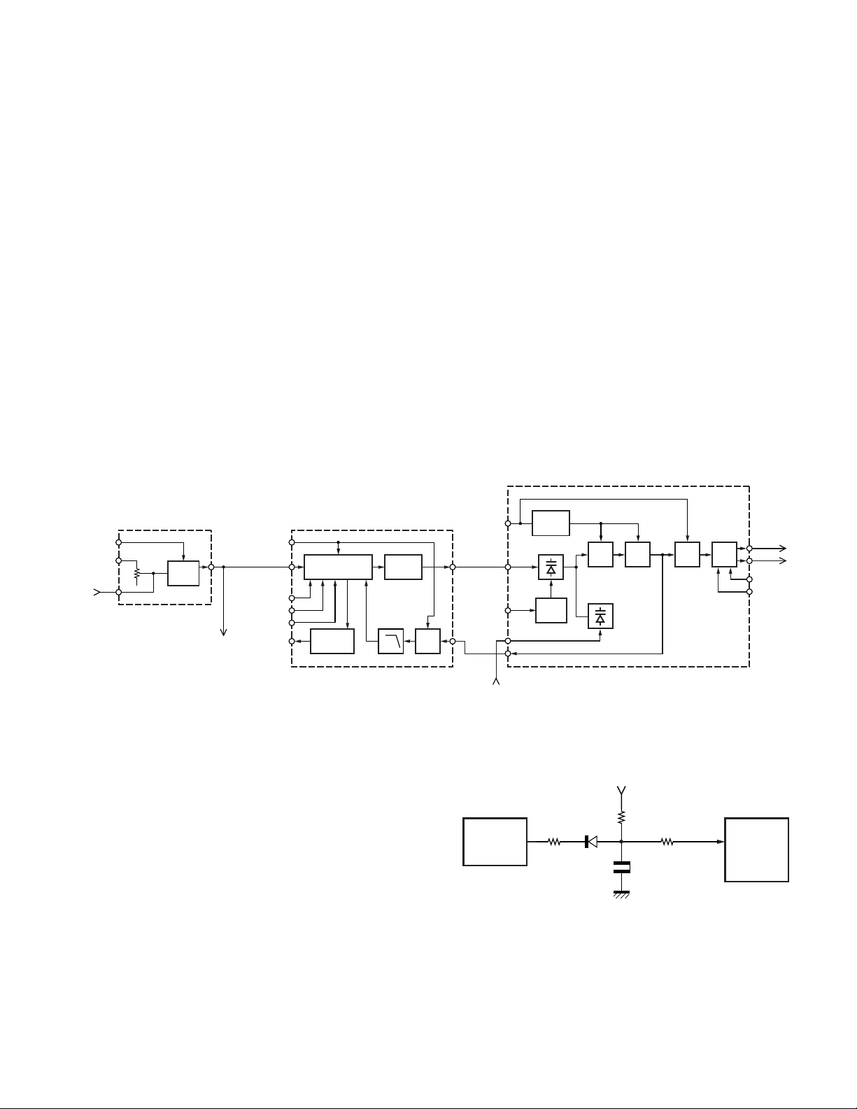
DISASSEMBLY FOR REPAIR
How to remove the case assembly from the chassis
1. Remove two screws (z) holding the chassis.
2. Pull out two knobs (
3. Pull out the SP and MIC parts of the cap from jacks (
4. Turn the unit over with the bottom of the chassis facing
upwards, and remove the chassis (
assembly (
5. Remove the speaker lead (
the TX-RX PC board (TX-RX unit A/3).
b
).
) and remove two round nuts (c).
x
) from the case
n
) from the connector (CN2) of
m
v
).
How to remove the PC board
■ Numeric key PC board (TX-RX unit B/3)
1. Remove three screws (,) on the numeric key PC board.
2. Lift the numeric key PC board and remove it from the
■ PTT PC board (TX-RX unit C/3)
3. Remove one screw on the PTT PC board (/).
4. Pull the PTT PC board to the left and remove it from the
■ TX-RX PC board (TX-RX unit A/3)
5. Remove the SP/MIC jack cover (≈).
6. Remove two screws (
7. Remove two screws (
8. Remove eight screws (
9. Absorb solder from the antenna terminal (
Note: Do not melt the shadow plate (
10.Remove the TX-RX PC board from the chassis, then remove
connector (CN9) of the TX-RX PC board (
.
).
connector (CN6) of the TX-RX PC board (TX-RX unit A/3)
(
Ω
).
) holding the shield
ç
cover (antenna terminal section).
) holding the shield
√
cover (final amplifier section).
board.
with a solder absorber.
) on the TX-RX PC
∫
µ
moving the tip of the solder absorber close
to the antenna terminal.
the encoder volume FPC (
of the TX-RX PC board.
) from the flat cable connector
≤
~
) when
)
2

TH-K2AT/K2E/K2ET
DISASSEMBLY FOR REPAIR
Soldering the antenna terminal
1. With the shield cover removed from the antenna terminal
section, install two screws on the PC board and bring the
PC board into contact with the chassis (
2. Solder the antenna terminal with a soldering iron (
z
).
).
x
x
z
3. Remove the two screws installed in step 1 above, and install
the two screws again on the PC board together with the
shield cover (
c
).
c
4. Apply the tips of soldering irons to all the four pins of the final
FET at the same time (
the final FET (
). (Two persons should be required to do this.)
v
v
5. Remove all PC boards from the chassis.
6. Confirm that there is no space between the radiation plate
installed on the foil side of the TX-RX PC board (TX-RX unit
A/3) and the PC board (
the radiation plate and PC board, eliminate it by applying
the tip of the soldering iron to the radiation plate.
), heat them sufficiently, and remove
c
c
). If there is any space between
b
b
Radiation plate
TX-RX PC board
Replacing the final FET (Q12)
1. Remove the two screws holding the shield cover of the
final FET section (
2. Remove solder from the shield cover completely with a
solder absorber. (E and E3 types only)
3. Remove the shield cover (
z
).
).
x
z
x
7. Apply the tip of the soldering iron to the installation side of the
radiation plate of the TX-RX PC board, put a little amount of
solder to the radiation plate that is seen through a square hole
in the final FET installation section and melt the solder (
8. When the solder in step 7 is melted, place the final FET on
the PC board by aligning it with the silk of the final FET
installation section of the PC board (
m
).
n
).
m
n
9. Release the soldering iron and confirm that the final FET
and radiation plate have been soldered.
10.Solder the four pins of the final FET with the soldering iron.
11.Install all the PC boards.
12.Reinstall the shield cover removed in step 3 above in its
original position and install two screws.
13.Solder the shield cover to the PC board. (E and E3 types
only)
14.
Install the chassis on the case assembly and assemble them.
15.Readjust transmission power.
Note: Since the FET is sensitive to static electricity, always
wear a grounding band. Use a highly insulated ceramic
heater solder iron.
3

TH-K2AT/K2E/K2ET
DISASSEMBLY FOR REPAIR
Special care and attention required for assembly
1. Gluing to the key top (MIC element section)
You must also glue on the speaker storage area and heap
the glue up until wealthy glued on the speaker storage area
and the key top for waterproofing the MIC element side of
the key top. (Fig. 1)
Heap the glue up until wealthy glued on the speaker
storage area and the key top (MIC element section).
Fig. 1
2.
Bending the LCD hardware fixture (J21-8456-03) tabs
(1)Insert the tabs of the LCD hardware fixture into four holes
in the LCD installing position of the TX-RX PCB (TX-RX unit
A/3). (Fig. 2)
Fig. 2
(2)By pressing the LCD hardware fixture from the component
side of the TX-RX PCB, you must bent all 4 tabs of the LCD
hardware fixture being visible from the foil side until the
bases of each tabs are folded at least 45 degrees (Fig. 3). If
the bending angle of the tabs of the LCD hardware fixture
is less than 45 degrees, a display error may occur.
Min 45
degrees
Bending position
NG
NG
Fig. 3
3. PTT PCB (TX-RX unit C/3) installation procedure
Installing the PTT PCB on the TX-RX PCB and chassis are
as follows:
(1)Insert the PTT PCB connector (CN7) into the TX-RX PCB
connector (CN6) lightly.
(2)Push three parts of the PTT PCB to contact tightly with the
chassis. There may be a small gap between the connectors.
(Fig. 4)
Note: A double-side adhesive tape (J99-0376-04) is used
behind the PTT switch. When reassembling the PTT
PCB to the chassis, press the PTT PCB (under the PTT
switch) so that the tape hold the PCB and chassis
securely.
Chassis
OK
PTT switch
Push three parts of the PTT PCB
to contact tightly with the chassis.
PTT PCB (C/3)
CN6
A bit
clearance
CN7
Chassis
NG
PTT switch
PTT PCB (C/3)
CN6
No
clearance
CN7
Fig. 4
(3)Tighten one screw in the PTT PCB.
4

TH-K2AT/K2E/K2ET
LAMP
LO
W
PTT
DISASSEMBLY FOR REPAIR
4. Packing (G53-1572-02) TX/BUSY lamp installation
procedure
(1)To assure waterproofing, install the packing in the chassis
groove as shown in Fig. 5. (
(2)Install the packing TX/BUSY lamp section on the chassis.
(
)
x
z
OK
Packing
Chassis
NG
Packing
Chassis
z
)
x
Cautions for installing the chassis on the case assembly
6.
(1)Verify that the packing (G53-1572-02) TX/BUSY lamp section
is has been past through the hole in the illumination guide
section on the top of the case assembly. (Fig. 7)
The packing TX/BUSY lamp section is has
been past through the hole in the illumination
guide section on the top of the case assembly.
Fig. 7
(2)Align the speaker lead as shown fig.8. Do not place the
leads over the key top section, LCD section or SP/MIC/DC
IN cap section.
Fig. 5
5.
Packing (G53-1572-02) bottom installation procedure
(1)Before installing the numeric key PCB (TX-RX unit B/3) on
the chassis, push three parts of the packing to contact tightly
with the chassis as shown in Fig. 6. If the packing is not in
contact with the chassis, there may be a gap between the
transceiver bottom case assembly and the battery, and
water may enter through the gap.
OK NG
Push three parts of the packing to
contact tightly with the chassis.
Clearance NG
Fig. 6
Do not fix this part of the
key top to the rib of the
case assembly.
Fig. 8
7.
Cautions for installing the key top on the case assembly
(1)Install the key top keypad section and the power switch
section on the rib of the case assembly.
(2)Do not fix the part between the key top keypad section and
the power switch section to the rib of the case assembly,
but install it as shown in Fig. 8.
5

TH-K2AT/K2E/K2ET
CIRCUIT DESCRIPTION
Frequency Configuration
The frequency configuration is shown in Figure 1 and
Table 1.
136.000~173.995MHz(K,K2,M,M2)
RX :
144.000~145.995MHz(E,E3)
TX :
ANT
ANT
SW
FINAL
DRIVE
144.000~147.995MHz(K,K2)
136.000~173.995MHz(M,M2)
144.000~145.995MHz(E,E3)
1st MIX
RF
AMP
PRE
DRIVE
144.000~147.995MHz(K,K2)
136.000~173.995MHz(M,M2)
144.000~145.995MHz(E,E3)
38.85MHz
174.850~212.845MHz
(K,K2,M,M2)
182.850~184.845MHz
(E,E3)
MCF
450kHz
CF
MIX, IF,
DET
Tripler
x 3
PLL
VCO
38.4MHz
AF
AMP
TCXO
MIC
AMP
SP
12.8MHz
MIC
Fig. 1 Frequency configuration
Double super heterodyne
Reception method 1st IF Frequency 38.85MHz (Upper)
2nd IF Frequency 450kHz (Lower)
Transmission method
VCO direct oscillation amplification
Modulation Variable reactance phase modulation
Table 1 Basic configuration
Receiver System
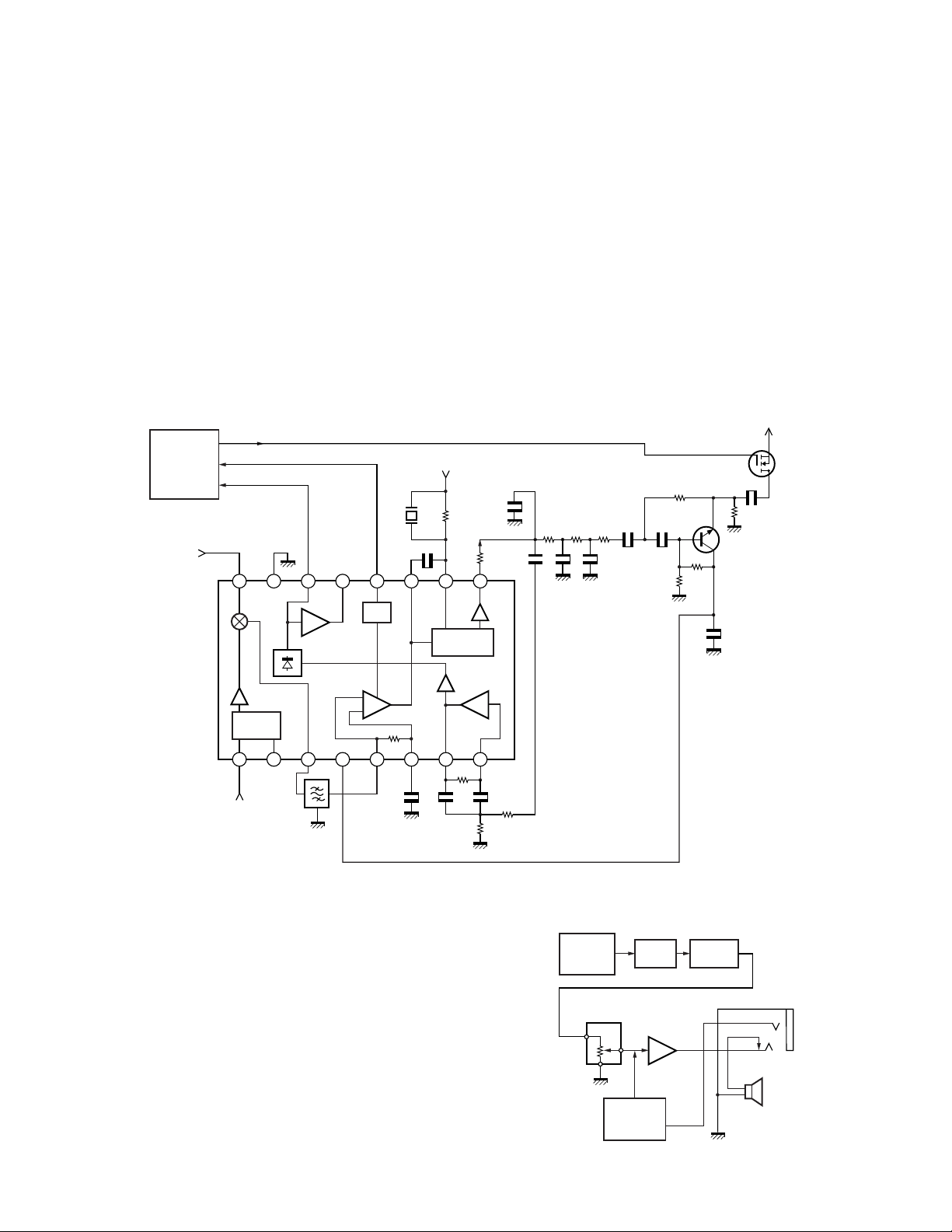
■ Front End
The received signal from the antenna passes through a lowpass filter and then through a transmission/reception switching
circuit (antenna switch) and enters the band-pass filter (L40,
L41, L38).
The signal passing through the band-pass filter (L40, L41,
L38) is amplified by with an RF amplifier (Q17), passes through
a band-pass filter (L32, L35) and enters the first mixer (Q16).
These band-pass filters are tuned to a desired frequency
by varicaps (D21, D20, D19, D18).
A tuning voltage corresponding to the desired signal is
applied to each varicap through the BPF/APC terminal (pin 6)
of the MPU (IC8) to tune to the receive frequency.
■ First Mixer
The received signal passing through the band-pass filter
(L32, L35) is mixed with the first local signal generated by the
VCO by the first mixer (Q16) to produce a first IF signal (38.85
MHz) (Upper heterodyne).
The first IF signal passes through a MCF (Monolithic crystal
filter: XF1) to remove unwanted components.
The first IF signal passing through the MCF (XF1) is amplified
by an IF amplifier (Q24) and the resulting signal enters the FM
IC (IC3).
Item Rating
Nominal center frequency (fo) 38.85MHz
Pass bandwidth ±6.0kHz or more at 3dB
Attenuation bandwidth ±25kHz or less at 35dB
Ultimate attenuation 70dB or more (fo –910 kHz)
Spurious response 40dB or more (fo +1MHz)
Ripple 1dB or less
Insertion loss 4dB or less
Terminating impedance 610Ω ±5% // 3pF ±0.5pF
Table 2 MCF (L71-0619-05) characteristics (TX-RX unit XF1)
Item Rating
Nominal center frequency (fo) 450kHz
3dB bandwidth ±6.5kHz or more
50dB bandwidth ±15.5kHz or less
Ripple 2dB or less (fo ±6.5kHz)
55dB or more
Guaranteed attenuation (fo ±18kHz to ±33kHz)
50dB or more (fo ±100kHz)
Insertion loss 4dB or less
I/O matching impedance 1.5kΩ
Table 3 Ceramic filter (L72-0968-05) characteristics (TX-RX unit CF1)
ANT
BPF
L41,L40,L38
ANT
SW
Tuning voltage
PLL
LV
LPF
VCO
6
RF AMP
Q17
D20D21
6
BPF/APC
MPU
IC8
Fig. 2 Receiver section configuration
D19
BPF
L32,L35
MIXER
D18
Q16
MCF
XF1
38.85MHz
1st Local OSC
(PLL)
IF AMP
Q24
5R5R
FM IC
IC3
IF AMP,
DET
2nd Local OSC
Tripler
x 3
TCXO
12.8MHz
AF AMP
IC6
Q23
X1
SP
TH-K2AT/K2E/K2ET
CIRCUIT DESCRIPTION
■ IF Circuit
The first IF signal (38.85 MHz) amplified by the IF amplifier (Q24)
and the second IF signal (38.4 MHz) generated by tripling the 12.8
MHz reference oscillator frequency of the TCXO (X1) by Q23, are
mixed in the FM IC to produce a second IF signal (450 kHz) (Lower
heterodyne).
The second IF signal passes through a ceramic filter (CF1)
to remove unwanted components.
The second IF signal passing through the ceramic filter (CF1)
passes through the IF amplifier in the FM IC again and is
detected to produced an audio signal.
■ Squelch and Mute Circuit
A noise component is obtained by passing FM detection
output (FM IC pin 9) through an operational amplifier in the
9
AFM
49
IC8
MPU
1st IF input
(38.85MHz)
SM
SQ
IC3
FM IC
2nd local OSC
(38.4MHz)
SMV
48
SQV
16 15 14 13 12 11 10 9
MIX
Noise
comp
Rectifier
Buffer
Local
OSC
1 2 3 4 5 6 7 8
CF1
450kHz
RSSI
IF AMP
5R
CD1
Quadrature
detector
C173 C174
Inverter
R135
R125
AF OUT
Noise
AMP
AMP
FM IC and band-pass filter consisting of R125, R126, R135,
C173, C174. The noise component is rectified in the FM IC to
produce a DC voltage, which is output from the N-REC terminal
(pin 14) of the FM IC as squelch voltage.
The squelch voltage enters the SQ terminal (pin 48) of the
MPU (IC8) and is compared with the reference voltage preset
in the MPU to control audio signal ON/OFF.
When "L" is output from the AFM terminal (pin 9) of the MPU,
the AF mute switch (Q20) is activated to mute the audio signal.
■ S Meter Circuit
The S meter voltage is output from the RSSI terminal (pin
12) of the FM IC (IC3) and input to the SM terminal (pin 49) of
the MPU. Then the voltage is converted from analog to digital
in the MPU to control the S meter display on the LCD.
VOL IN
Q20
AF MUTE
SWITCH
Q21
AF FILTER
LPF
R126
5R
Fig. 3 IF, Squelch, Mute and S meter circuit
■ AF Amplifier
The detected audio signal passes through an AF filter (Q21)
and enters an AF mute switch (Q20).
After passing through the AF mute switch (Q20), the signal
passes through an AF volume (VR201) and is amplified to a
specified output level with an AF amplifier (IC6).
The audio signal amplified with the AF amplifier (IC6) is
output through an internal speaker or an external speaker
jack (J4).
The beep tone and the DTMF signal are output from the
DTMF/BEEP terminal (pin 40) of the MPU (IC8), enters the AF
amplifier (IC6) and is output as a monitor tone.
IC3
FM IC
9
AF OUT
VR201
AF VOLUME
40
DTMF/BEEP
IC8
MPU
Q21
AF
FILTER
IC6
AF AMP
REM
46
Q20
AF MUTE
SWITCH
SPG
REM/TXD
SPK
AFO
Fig. 4 AF amplifier
J4
SP JACK
SP
7

TH-K2AT/K2E/K2ET
CIRCUIT DESCRIPTION
Transmitter System
■ Microphone Amplifier Circuit
The audio signal from the microphone passes through a
high-pass filter (IC5) and enters a microphone amplifier (IC16).
The signal passes through a pre-emphasis circuit, limiter
amplifier and splatter filter inside the microphone amplifier.
The splatter filter will remove distortion outside the audio band.
IC16
MIC AMP
MIC IC5
61
HPF
emphasis
Fig. 5 Microphone amplifier circuit
■ Modulation Circuit
The audio signal amplified by the microphone amplifier
(IC16) passes through a semi-fixed volume (VR5) for
modulation adjustment, and goes to the VCO modulation
varicap (D6) for variable reactance phase modulation.
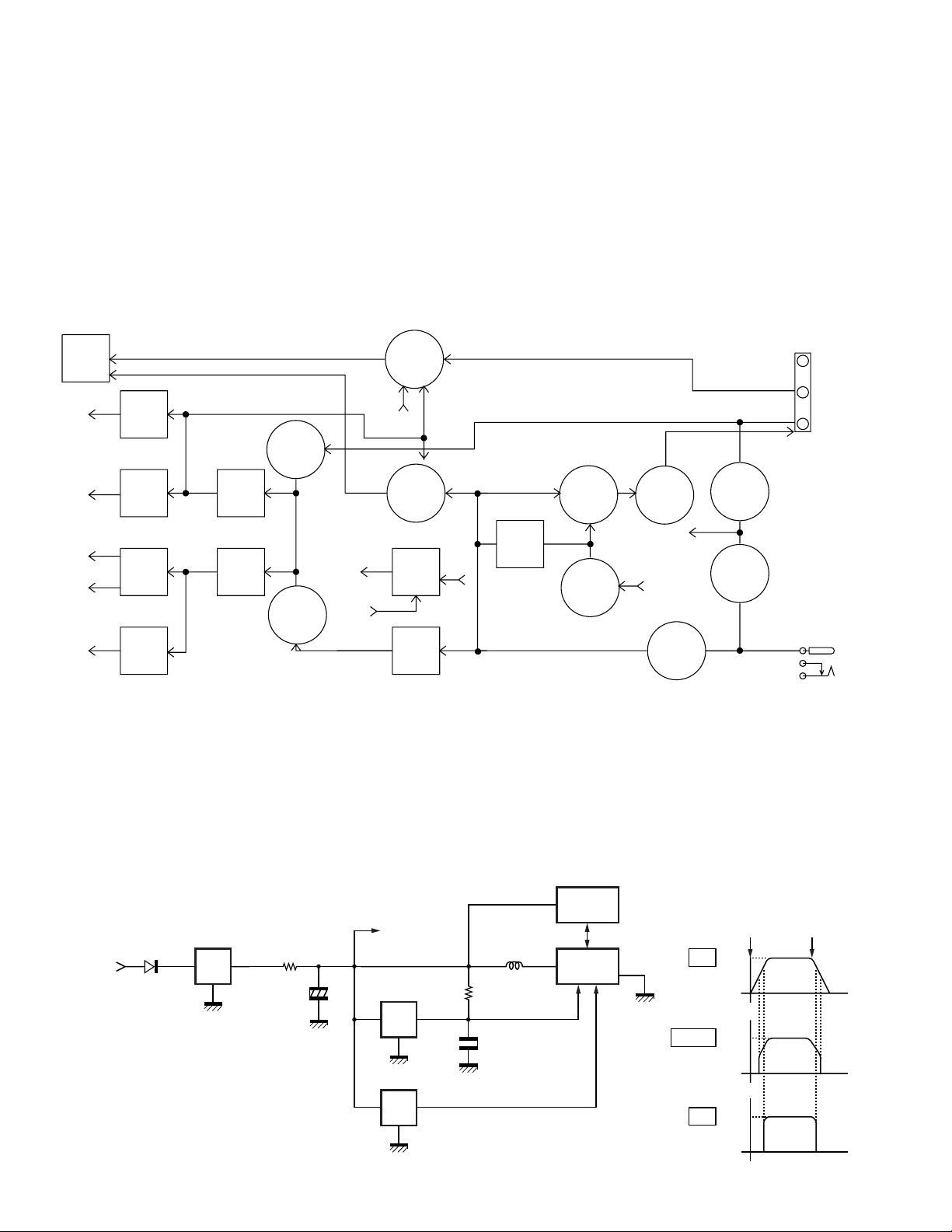
■ Drive and Final Circuit
The output signal from VCO (Q1) passes through an RF
amplifier (Q2, Q5, Q9) and drive amplifier (Q10, Q11), and is
amplified by a power amplifier (Q12).
■ Transmission/Reception Switching Circuit
The signal amplified by the power amplifier (Q12) passes
through a transmission/reception switching circuit and a lowpass filter, and is fed to the antenna.
Q11
Q10
Pre-
Limiter
VCO
Splatter
filter
Q12
The transmission/reception switching circuit consists of D10,
L19, D12 and D13. These diodes are turned ON in transmit
mode and OFF in receive mode to switch signals.
MIC
IC5
HPF
AMP
DRIVE AMP
Q10
DRIVE AMP
IC16
MIC
Q11
VR5
MAX DEV
Q12
POWER AMP
Q1
VCO
Q2
RF AMP
D10,L19
D12,D13
ANT
SW
RF AMP
LPF
Q5
ANT
Q9
RF AMP
Fig. 6 Modulation, Drive, Final and
Transmission/reception switching circuit
■ APC Circuit
The APC (Automatic Power Control) circuit is used to obtain
a stable transmission power and controls transmission output
by detecting the drain current of Q11 and Q12.
The transmission output can be changed in three levels:
High, Mid, and Low.
The reference voltage is output from the BPF/APC terminal
(pin 6) of the MPU (IC8) and the detection voltage generated by
R70, R71 and R72 are fed to the APC differential amplifier (IC2).
The voltage in proportion to the difference between
reference voltage and detection voltage is output from the
BOUT terminal (pin 7) of IC2 as an APC voltage.
ANT
D10
LPF
L19
D13
RX
Q55
–t
TH1
+
51
THERM
7
KAPC
6
BPF/APC
IC8
MPU
FINAL
16
Q58
D12
VGG
Q15
5T
R72
R71
R70
B
Q13
B
8
Fig. 7 APC and Temperature protection circuit
1
2
3
4
VDD
APC AMP
AOUT
A–IN
A+IN
GND
IC2
BOUT
B–IN
B+IN
8
V+
7
6
5
Q14
TH-K2AT/K2E/K2ET
Fo/LD
PLL LD
IC8
MPU
IC1
PLL IC
R32
D16
C40
R35
14
102
5C
CIRCUIT DESCRIPTION
The APC voltage controls the gate voltage of Q11 and Q12,
and keeps transmission output stable.
The MPU detects power supply voltage and controls Q58
by transmission power supply voltage and transmission power.
For example, if the power supply voltage during transmission,
is equal to or higher than approx. 10.5 V and if power is at Mid
or Low level, the APC voltage level applied to Q12 is reduced
by Q58.
■ Temperature Protection Circuit
To prevent thermal destruction of the power amplifier (Q12),
this circuit reduces APC voltage when Q12 temperature rises.
The MPU (IC8) detects temperature with a thermistor (TH1)
and controls reference voltage to the APC circuit.
PLL System
■ PLL Circuit
A reference frequency of 5 kHz or 6.25 kHz is produced by
dividing the 12.8 MHz reference frequency of the TCXO (X1)
with PLL IC (IC1). Comparison frequency is produced by
TO
5C
5/0V
5MS
5/0V
TCXO
VR1
VC
X1
TCXO
12.8MHz
12.8MHz
IF
5C
5/0V
CLOCK
DATA
Fo/LD
PLL
IC1
PLL IC
LE
Rectifier
LOOP
FILTER
LPF Q6
amplifying VCO output with an RF amplifier (Q6) and dividing
it with the PLL IC.
The PLL synthesizer with 5 kHz and 6.25 kHz step is
configured by comparing phases of the reference frequency
and comparison frequency.
The phase difference between reference frequency and
comparison frequency passes through a charge pump in the
PLL IC, then ripples are removed with a loop filter with lowrange passing characteristics to produce VCO control voltage
(lock voltage).
■ VCO Circuit
The VCO produces a desired frequency directly with a
Colpits oscillation circuit containing an oscillation transistor (Q1)
used for both transmission and reception.
The VCO control voltage is applied to varicap (D1, D2) to
produce a desired frequency.
The SHIFT terminal (pin 113) of the MPU (IC8) goes "H"
during reception, and the shift control switch (Q3) is turned
ON to change oscillation frequency.
VCO
Q4
Ripple
D1,D2
Q3
SHIFT
Filter
SW
Q1
OSC
MOD
Q2
Buff
Amp
Q5
Amp
RF
RF
Amp
LV
1~5V
5C
5/0V
SHIFT
H/L
D8,D9
SW
TX
RX
5T 5/0V
5R 5/0V
Fig. 8 PLL and VCO circuit
■ Unlock Detection Circuit
When the PLL is unlocked, the waveform of the pulse
output from the Fo/LD terminal (pin 14) of the PLL IC (IC1) is
rectified with R32, D16, R35 and C40, and the Fo/LD terminal
is made “L” level. The voltage at the Fo/LD terminal is
detected by the MPU to control transmission/reception
switching timing.
MOD
Fig. 9 Unlock detection circuit
9
TH-K2AT/K2E/K2ET
CIRCUIT DESCRIPTION
Power Supply Circuit
■ Charging Circuit
When an external power supply is connected to the DC IN
terminal, the constant-current circuit consisting of Q33 and
D31 provides a constant current of approx. 110 mA to the NiMH battery.
If no external power supply is connected to the DC IN
terminal, the constant-current circuit does not function.
IC8
MPU
BTEMP
DCDET
VR1
ENC
IC1
TCXO
Q4,5,6
D40,41
IC5
Q30
IC3,17
D9,14
Q16,17
Q22,23,24
Q59
Q9,10,13
D8,10
TH1
IC16
Q47
5MS
5MV
5C
5R
5T
Q41
RN2105
5MS SW
Q57
RN2105
5C SW
Q53
RN2701
5R SW
5MV SW
Q55
CPH3317
5T SW
5M
IC9
TK11250
CM
AVR
5.0V
IC12
TK11250
CUCB
AVR
5.0V
D35
RB521S-30
PROTECT
D36
RB521S-30
PROTECT
IC6
D48,49
D42,43,46
D47,44
AF AMP
Q36
2SJ347
THERM
DET
BTDET
Q35
2SK1830
DC-IN
DET
Q37, Q38
2SB1184
(Q,R)
2SC4617(R)
AF/LAMP
AVR
IC4
XC6202PB
52FR
AVR
11.5V
■ Power Supply Switching Circuit
The voltage supplied through the battery terminal or DC IN
terminal is branched in the power supply switching circuit as
shown in Fig.10 and then supplied to the required components.
■ Battery Type Recognition Circuit
When the battery pack is attached to the transceiver, the
battery type is recognized with the T terminal on the
transceiver. This battery type recognition activates charging
for the Ni-MH battery pack and displaying the battery meter.
-
T
+
BATT TERMINAL
7.5V Norminal
(6.0 - 9.0V)
Q33
2SB1184
(Q,R)
BATT
D31
DA221
CONSTANT
CURRENT
B
CHARGE
Q34
2SK1830
CHARGE
SW
D30
RB521S-30
PROTECT
CHARGE
D80
RB521S-30
PROTECT
D33
RB051L-40
PROTECT
B
D32
RB051L-40
PROTECT
DC IN
13.8V Norminal
(12.0 - 16.0V)
B
J2
Fig. 10 Charging and Power supply switching circuit
Control System
■ Reset and Backup Circuit
When power is supplied to the transceiver, the 5M voltage
goes “H” as C303 is charged.
A rising edge of the 5M voltage is detected by the voltage
detection IC (IC11) and when its output (RESET) goes “H”,
the reset status of the MPU is released.
5C
IC11
IN OUT
IC10
IN OUT INT
BATT
D35
IC9
IN OUT
5V
AVR
R244
C303
5M
+
If the supplied voltage to the transceiver is reduced and
the 5M voltage falls below the detection voltage of the voltage
detection IC (IC10), the MPU detects it by an interrupt
processing, backs up data in EEPROM (IC15) and turns the
power off.
Timing chart
Power
ON
5V5M
0
5VRESET
0
5VINT
Power
OFF
R243
C307
L63
IC15
EEPROM
IC8
MPU
RESET
10
0
Fig. 11 Reset and Backup circuit

TH-K2AT/K2E/K2ET
CIRCUIT DESCRIPTION
■ Voltage Detection Circuit
Various voltages are input to the A/D port of the MPU (IC8)
for processing.
Battery voltage is divided with resistors (R240, R241) and
enters the BATT terminal (pin 52) of the MPU.
Battery voltage is used for battery meter indication during
transmission or for alert tone processing when an abnormal
power supply voltage (approx. 16.5 V or higher) is applied.
Squelch voltage becomes DC voltage by detecting changes
in noise voltage in the FM IC (IC3), and the signal is used for
squelch control.
The S meter voltage is output from the RSSI pin of the FM
IC to control S meter display.
Detection of thermistor voltage (temperature) in the Ni-MH
battery during charging, detection of remote microphone key
pressing and VOX voltage monitoring are performed through
each A/D port of the MPU.
■ Battery Save Circuit
If there is no signal (squelch off, scan off or no key operation)
for longer than 10 seconds, the transceiver will enter the
battery save mode.
Battery save operation is performed by controlling Q57 with
an output signal from the 5C (SAVE) terminal (pin 15) of the
MPU.
The 5C ON/OFF cycle ratio during battery saving can be set
from a transceiver menu.
■ LED Drive Circuit
The LCD and key illumination LEDs are lighted by controlling
Q51 for the LCD and Q50 for keys according to the output
voltage from the AF/LAMP AVR (Q37).
The BUSY and TX illumination LEDs are lighted by controlling
Q47.
Q47
D46
Q51
56
99
LAMP
RX LED
5T
AF AMP
D33
Q38
Q37
D48
D42
D42
D42
D44
D49
D43
D43
D43
D47
Q50
D41
BUSY LED
5C
TX LED
D40
R227
R226
B
Fig. 13 LED drive circuit
IC8
MPU
5MS
Q41
37
5MS
5C (SAVE)
IC8
MPU
5C
Q57
15
Fig. 12 Battery save circuit
5M
11

TH-K2AT/K2E/K2ET
CIRCUIT DESCRIPTION
■ Key and Encoder Input Circuit
The POWER key is assigned to the interrupt port (pin 95) of
the MPU.
The PTT key is assigned to the dedicated port (pins 13, 14)
of the MPU.
16 key (K, K2, M, M2 and E3 types)
KIN1 KIN2 KIN3 KIN4
KIN0 KOUT0 KOUT1 KOUT2 KOUT3
MENU
F321
LAMP
VFO654
MONI
MR987
SET
CALL
∗
#0
Other keys composes a matrix and key presses are detected
by scanning them by software.
The encoder reads data using the interrupt port (pins 35
and 36) of the MPU.
IC8
MPU
PWRSW
SW
PTTI14PTTE13ENCB36ENCA
95
S7POWER
35
ROTARY
ENCODER
4 key (E type)
IC8
KIN0 KOUT0 KOUT1 KOUT2 KOUT3
KIN1 KIN2 KIN3 KIN4
MRVFOF
MENUCALL
LAMP
MONI
SET
MPU
Fig. 14 Key and Encoder input circuit
PWRSW
POWER
SW
J3
PTTI14PTTE13ENCB36ENCA
95
S7
J3
35
ROTARY
ENCODER
12

TH-K2AT/K2E/K2ET
CIRCUIT DESCRIPTION
■ CTCSS/DCS
The encode signal is generated by the MPU (IC8) and output
from the TONE terminal (pin 41) of the MPU.
The unwanted high-frequency components of the encode
signal output from the MPU are removed with a low-pass filter,
and applied to VCO modulation input (MOD) and TCXO VC
terminal for modulation.
The VCO and TCXO modulation levels are adjusted by VR6
to produce flat modulation characteristics in low and high
ranges.
The decode signal is input to the SIGIN pin (pin 47) of the
MPU after the waveform of the audio signal from the FM IC is
rectified with a CTCSS/DCS filter (IC17). Then the set CTCSS
tone frequency and DCS code are detected by digital signal
processing in the MPU to control muting.
X1
TCXO
VC
VCO
VR6
MOD
VR5
1
MIC
AMP
6
LPF
AMP
IC16
50
■ DTMF
The DTMF signal is generated by the MPU (IC8) and is
output from the DTMF/BEEP terminal (pin 40) of the MPU.
The DTMF signal is mixed with an audio signal at the input
side of the AF amplifier (IC6), and is output as a monitor tone.
The DTMF signal is mixed with a modulation signal at the
input side of pre-emphasis in the microphone amplifier (IC16)
and used as a transmit signal.
■ VOX
The IC5 and Q30 amplify the audio signal captured in the
microphone, and then the signal is converted into the DC
Voltage D24 rectifies.
The DC voltage activates the MPU (IC8), and the VOX starts.
■ Weather Alert (K and K2 types only)
The IC17 apmlifies the detected signal from the FM IC (IC3),
and the MPU (IC8) processes the signal. This signal processing
activates Weather Alert function.
41
TONE
SIG INVOX IN
IC8
MPU
DTMF/BEEP
40
111
NOAA K, K2 types only
47
CTCSS/DCS
IC17D24Q30 IC3
9
FILTER
FM
IC
MIC
IC5
HPF
IC6
AF AMP
Vin
VOL OUT
Fig. 15 CTCSS/DCS, DTMF, VOX, Weather alert
■ Serial Control
Serial control must be enabled from a transceiver menu so
that the REM/TXD pin of the speaker jack (J4) and the PTT
(RXD) pin of the microphone jack (J3) function as TXD and
RXD, respectively, when communicating with a personal
computer.
MIC JACK
J3
J4
SP JACK
PTT
MIC
IM
REM/TXD
SP
5MS
SPG
SPK
AFO
IC5
HPF
5MC
10
+
–
POUT
IC6
AF AMP
MIC
46
REM
IC8
MPU
13
PTTE
TXD
RXD
12
11
Fig. 16 Serial control
13

TH-K2AT/K2E/K2ET
SEMICONDUCTOR DATA
MPU : 90522BPFFG139 (IC8)
■ Pin function
Pin Pin
No. Name
1 CLOCK O Common serial clock output
2 DATA O Common serial data output
3 EEPDI I Data input from EEPROM
4 EEPCS O Chip select output to EEPROM
5 VOX O VOX power supply switch L:ON
BPF/APC
6
7 KAPC O APC ON/OFF switch L:APC ON
8 VCC - Positive power supply
9 AFM O AF mute switch L:Mute
10 SPM O Speaker mute switch H:Mute
11 RXD I UART data input line from PC (9600bps)
12 TXD O UART data output line to PC (9600bps)
13 PTTE I External [PTT] key input L:ON
14 PTTI I [PTT] key input L:ON
15
5C(SAVE)
16 FINAL O
17 SEG0 O LCD segment output 0
18 SEG1 O LCD segment output 1
19 SEG2 O LCD segment output 2
20 SEG3 O LCD segment output 3
21 SEG4 O LCD segment output 4
22 SEG5 O LCD segment output 5
23 SEG6 O LCD segment output 6
24 SEG7 O LCD segment output 7
25 SEG8 O LCD segment output 8
26 SEG9 O LCD segment output 9
27 SEG10 O LCD segment output 10
28 SEG11 O LCD segment output 11
29 SEG12 O LCD segment output 12
30 SEG13 O LCD segment output 13
31 SEG14 O LCD segment output 14
32 SEG15 O LCD segment output 15
33 VSS - GND
34 COR1
35 ENCA I Encoder A side input
36 ENCB I Encoder B side input
37 5MS O 5MS main power supply switch L:ON
38 DVCC - Reference voltage input for DAC
39 DVSS - Ground for DAC
DTMF/
40
BEEP 1750Hz (D/A)
41 TONE O
42 AVCC - Positive power supply for ADC
43 AVRH - Reference voltage input for ADC
44 AVRL - Ground reference voltage input for ADC
45 AVSS - Ground for ADC
46 REM I
47 SIGIN I
14
I/O Function
BPF tuning voltage output, APC voltage
O
output (PWM)
O Save power supply switch L:ON
Gate bias control of TX final amplifier
L:Bias ON
- Power supply stabilization (Connected to
VSS through 0.1uF)
Encode waveform output of DTME/BEEP/
O
Encode waveform output of CTCSS/DCS
(D/A)
Remote control microphone key voltage
input (A/D)
Decode waveform input of CTCSS/DCS
(A/D)
Pin Pin
No. Name
48 SQ I Noise voltage input for squelch (A/D)
49 SM I RSSI voltage input for S-meter (A/D)
50 VOXIN I Microphone voltage input for VOX (A/D)
51 THERM I TX temperature compensation input(A/D)
52 BATT I Battery voltage input (A/D)
53 BTEMP I
54 VCC - Positive power supply
55
CHARGE
56 LAMP O Lamp power supply switch H:ON
57 AFAMP O
58 NAR O Wide/Narrow switching H:Narrow
59 COM0 O LCD common output 0
60 COM1 O LCD common output 1
61 COM2 O LCD common output 2
62 COM3 O LCD common output 3
63 VSS - GND
64 SEG16 O LCD segment output 16
65 SEG17 O LCD segment output 17
66 SEG18 O LCD segment output 18
67 SEG19 O LCD segment output 19
68 SEG20 O LCD segment output 20
69 SEG21 O LCD segment output 21
70 SEG22 O LCD segment output 22
71 SEG23 O LCD segment output 23
72 SEG24 O LCD segment output 24
73 NC - Not used
74 NC - Not used
75 SEG25 O LCD segment output 25
76 SEG26 O LCD segment output 26
77 SEG27 O LCD segment output 27
78 SEG28 O LCD segment output 28
79 SEG29 O LCD segment output 29
80 SEG30 O LCD segment output 30
81 SEG31 O LCD segment output 31
82 V0 - Not used
83 V1 - Not used
84 V2 - Not used
85 V3 - LCD drive power supply 3
86
HST(VCC)
87 MD2 I L fixed
88 MD1 I H fixed
89 MD0 I H fixed
90 RESET I Reset input L:Reset
91 VSS - GND
92 X0 I System clock (7.9872MHz)
93 X1 O System clock (7.9872MHz)
94 VCC - Positive power supply
95 PWRSW I Power switch interrupt input (↓)
96 INTUP I Power supply voltage interrupt input (↑)
97 INTDW I Power supply voltage interrupt input (↓)
I/O Function
Detection of thermistor voltage (temperature)
in the Ni-MH battety (A/D)
Battery charge circuit power supply switch
O
AF amplifier/Lamp AVR power supply
switch H:ON
I Not used (VCC)
H:ON

TH-K2AT/K2E/K2ET
SEMICONDUCTOR DATA / COMPONENTS DESCRIPTION
Pin Pin
No. Name
98 DCDET I
99 RXLED O Busy LED output H:ON
100 BSFT O Beat shift swiching output H:ON
101 PLLEN O Serial enable output to PLL IC
102 PLLLD I
103 KIN0 I Key matrix input 0
104 KIN1 I Key matrix input 1
105 KIN2 I Key matrix input 2
106 KIN3 I Key matrix input 3
107 KIN4 I Key matrix input 4
108 TYPE I Market code bit input
109 VUKEY I Detection of 4 key or 16 key
110 MICM O Microphone mute switch H:Mute
111 NOAA I 1050Hz tone detection input
112 5R O RX power supply switch L:ON
113 SHIFT O VCO shift switch L:TX, H:RX
114 5T O TX power supply switch L:ON
115 KOUT0 O Key matrix output 0
116 KOUT1 O Key matrix output 1
117 KOUT2 O Key matrix output 2
118 KOUT3 O Key matrix output 3
119 VSS - GND
120 BTDET O Battery detection switch L:ON
I/O Function
DC IN detection interrupt input (↓)
L:DC IN connected
Lock detection input from PLL IC H: Lock
COMPONENTS DESCRIPTION
TX-RX UNIT (X57-674X-XX)
Ref. No.
IC10
IC11
IC12 5.0V AVR
IC15 EEPROM
IC16
IC17
Q5,6,9 RF amplifier
Q10,11
Q12
Q13
Q14
Q15
Q16 1st mixer
Q17
Q20
Q21 Audio filter Active filter
Q22
Q23 Tripler 2nd local
Q24 IF amplifier 1st IF 38.85MHz
Q27
Q29
Q30
Q31
Q33
Use/Function
IC1 PLL IC
APC differential
IC2
amplifier
IC3 FM IC
IC4 11.5V AVR
IC5 HPF Active filter
IC6 AF amplifier
IC8 MPU
IC9 5.0V AVR
4.4V voltage
detection
3.3V voltage
detection
MIC amplifier
CTCSS/DCS/WX
filter
Q1 VCO
Q2 RF amplifier
VCO shift
Q3
control switch
Q4 Ripple filter
Drive amplifier
Power amplifier
APC circuit
operation switch
APC output
switch
Q10 operation
switch
RX 1st amplifier
Audio mute
switch
Wide/narrow
changeover switch
Wide/narrow
changeover switch
MIC mute
switch
VOX detection
amplifier
Q56 operation
switch
Charge switch
Operation/Condition/Compatibility
MPU INT voltage detection
MPU Reset voltage detection
Limiter, splatter filter
Active filter
On RX
On TX
On TX
On TX
Audio mute when off
On when wide is selected
On when wide is selected
Mutes when ON
Off when the speaker outputs audio
15

TH-K2AT/K2E/K2ET
COMPONENTS DESCRIPTION
Ref. No.
Q34
Q35
Q36
Q37
Q38
Q41 5MS switch On when 5MS is applied
Q47
Q50
Q51
Q52
Q53
Q55 5T switch On when 5T is applied
Q56
Q57 5C switch On when 5C is applied
Q58
Q59
D1,2
D10-13
D14
D15
D16
D17
D18-21
D22
D24
D25
D26
D27
D30
D31
D32
Use/Function
Q33 operation
switch
DC IN detection
Ni-MH temperature
detection
AF amplifier/
Lamp AVR
Q37 operation
switch
TX/BUSY LED
switch
Key LED switch
LCD LED switch
Beat shift switch
5R/5MV switch
Speaker mute
switch
Q12 gate
voltage switch
WX detection
amplifier
VCO frequency
control
D5
Frequency shift
D6
VCO modulation
D7 Speed up Ripple filter
D8 RF switch On TX
D9 RF switch On RX
Antenna switch
Reverse current
prevention
APC output
voltage limiter
PLL lock detection
Over input
protection
RX BPF tuning
MIC mute control
VOX detection
rectification
Speaker mute
speed up
C246 discharge
MIC ALC
rectification
Reverse current
prevention
Constant-current
circuit
Reverse current
prevention
Operation/Condition/Compatibility Ref. No.
On when charging
H: DC IN detection
On when temperature detection is
activated
On when the speaker outputs audio or
lamp lights
On when the key LED lights
On when the LCD LED lights
On when 5R or 5MV is applied
Off when High power is selected
On TX
APC reference voltage
Charge current
Constant-current charge
DC IN
Use/Function
Reverse current
D33
prevention
AVR
D34
constant-voltage
Reverse current
D35
prevention
Reverse current
D36
prevention
D40 TX LED Lights on TX
D41 BUSY LED Lights on RX
D42-44
D46,47
D48,49
D62-65
D69-72
D74,79 Limiter
Key illumination
LED
LCD illumination
LED
Key type
D60
detection
market code
detection
Reverse current
prevention
D73 Voltage drop
Reverse current
D80
prevention
Operation/Condition/Compatibility
Battery
Battery
DC IN
Key backlight illumination
LCD backlight illumination
Key matrix
16
PARTS LIST
New Parts. indicates safety critical components.
∗
Parts without Parts No. are not supplied.
Les articles non mentionnes dans le Parts No. ne sont pas fournis.
Teile ohne Parts No. werden nicht geliefert.
TH-K2AT/K2E/K2ET (Y50-580X-XX)
TX-RX UNIT (X57-674X-XX)
Ref. No.
1 3A,2G * A02-3817-02 CABINET ASSY(BATTERY CASE) K2,M2
21C*A02-3818-23 CABINET ASSY(4KEY) E
31A*A02-3819-23 CABINET ASSY(16KEY) K,K2,M
31A*A02-3819-23 CABINET ASSY(16KEY) M2,E3
4 3A,3C * A10-4066-11 CHASSIS
5 3B,3D * A82-0053-02 REAR PANEL
6 1B,1D * B09-0675-03 CAP(SP/MIC/DC IN)
7 1A,1C * B10-2746-03 FRONT GLASS
8 1B,1D * B11-1805-03 ILLUMINATION GUIDE(LCD)
9 2B,2D * B11-1806-04 FILTER(LCD)
10 1B,1D * B38-0881-05 LCD
11 1G * B62-1695-00 INSTRUCTION MANUAL(CHINESE) M2
11 1E,1G * B62-1696-00 INSTRUCTION MANUAL(ENGLISH)
11 1E,1G * B62-1697-00 INSTRUCTION MANUAL(SPANISH) K,K2,E
11 1E * B62-1697-00 INSTRUCTION MANUAL(SPANISH) E3
11 1E * B62-1699-00 INSTRUCTION MANUAL(GERMAN) E,E3
11 1E * B62-1702-00 INSTRUCTION MANUAL(ITALIAN) E,E3
11 1E * B62-1757-00 INSTRUCTION MANUAL(FRENCH) E,E3
11 1E * B62-1758-00 INSTRUCTION MANUAL(DUTCH) E,E3
12 3A * B72-2128-04 MODEL NAME PLATE(TH-K2AT) K,K2,M
12 3A * B72-2128-04 MODEL NAME PLATE(TH-K2AT) M2
12 3C * B72-2129-04 MODEL NAME PLATE(TH-K2E) E
12 3A * B72-2193-04 MODEL NAME PLATE(TH-K2ET) E3
13 2B,2D * E04-0443-05 RF COAXIAL RECEPTACLE(SMA)
14 2A,2C * E23-1234-04 TERMINAL(BATTERY)
15 2B,2D * E29-1199-04 INTER CONNECTOR(LCD)
16 1A,1C * E37-1106-05 LEAD WIRE WITH CONNECTOR(SP)
17 2A,2C * F10-2464-04 SHIELDING COVER(FINAL FET)
18 2A,2C * F10-2465-04 SHIELDING COVER(ANT TERMINAL)
19 2B,2D * F15-1008-04 SHADOW PLATE(LCD)
-*G10-1317-04 FIBROUS SHEET(SP NET)
21 3B,3D G53-1529-04 PACKING(VOL/ENC)
22 2A,2C * G53-1572-02 PACKING(CASE)
23 2B,2D * G53-1589-03 PACKING(SP/MIC)
24 3E * H52-1960-02 ITEM CARTON CASE(TH-K2AT) K,M
24 3E * H52-1961-02 ITEM CARTON CASE(TH-K2E) E
24 3E * H52-1962-02 ITEM CARTON CASE(TH-K2ET) E3
25 2H * H52-2009-02 ITEM CARTON CASE(TH-K2AT) K2,M2
26 2F * H12-3146-01 PACKING FIXTURE K,M,E
26 2F * H12-3146-01 PACKING FIXTURE E3
27 3G * H12-3147-03 PACKING FIXTURE K2,M2
28 2A,2C * J19-5451-03 HOLDER(TERMINAL)
29 1B,1D * J21-8456-03 HARDWARE FIXTURE(LCD)
30 2E,3G * J29-0709-04 BELT HOOK ASSY ACCESSORY
31 2A,2C * J30-1284-04 SPACER(PTT KNOB)
32 3E,2G J69-0342-05 HANDSTRAP ACCESSORY M,M2,E
32 3E J69-0342-05 HANDSTRAP ACCESSORY E3
33 2B,2D J82-0076-05 FPC(VOL/ENC)
45 3A,3C J99-0376-04 ADHESIVE TAPE
34 1B,1D K29-5150-03 KNOB(VOL)
35 1B,1D K29-5159-03 KNOB(ENC)
E : TH-K2E K : TH-K2AT M : TH-K2AT
E3 : TH-K2ET K2 : TH-K2AT M2 : TH-K2AT
Address
New
Parts No. Description
parts
TH-K2AT/K2E/K2ET
Destination Destination
TH-K2AT/K2E/K2ET
L:
Scandinavia
Y:
PX (Far East, Hawaii)
Y:
AAFES (Europe)
Ref. No.
36 1A * K29-9272-02 KEY TOP(16KEY) K,K2,M
36 1A * K29-9272-02 KEY TOP(16KEY) M2,E3
37 1A,1C * K29-9274-03 KNOB(PTT/LAMP/MONI)
38 1C * K29-9276-02 KEY TOP(4KEY) E
A 2B,2D N09-1492-05 PAN HEAD SCREW(SMA)
B 1B,1D N14-0569-04 CIRCULAR NUT(VOL/ENC)
C 1B,1D N14-0573-04 CIRCULAR NUT(SMA)
D 1A,1C N79-2035-46 PAN HEAD TAPTITE SCREW(PCB)
E 2A,2C N79-2040-45
F 3A,3C N82-2007-46 PAN HEAD TAPTITE SCREW(CASE)
G 2A,2C N09-2433-05
39 2B,2D R39-0602-05 VARIABLE RESISTOR
40 1A,1C T07-0341-15 SPEAKER
41 2F,3G * T90-1018-25 HELICAL ANTENNA ACCESSORY
42 2F * W08-0959-15 CHARGER(230V/13.8V) ACCESSORY M,E,E3
43 2E * W08-0960-15 CHARGER(120V/13.8V) ACCESSORY K
44 2E * W09-0991-05
44 2E * W09-0991-05
Address
0-11 : K, K2 0-21 : M, M2 2-71 : E 2-72 : E3
D40 B30-2156-05 LED(RED)
D41 B30-2157-05 LED(YELLOW)
D42-44 B30-2205-05 LED(YG) E3
D42-44 B30-2205-05 LED(YG) K,K2,M
D42-44 B30-2205-05 LED(YG) M2
D42,43 B30-2205-05 LED(YG) E
D46 B30-2205-05 LED(YG) E
D46,47 B30-2205-05 LED(YG) E3
D46,47 B30-2205-05 LED(YG) K,K2,M
D46,47 B30-2205-05 LED(YG) M2
D48,49 B30-2237-05 LED(YG)
C1 CK73HB1C103K CHIP C 0.010UF K
C2 CK73HB1H102K CHIP C 1000PF K
C3 CC73GCH1H030B CHIP C 3.0PF B
C4 CK73HB1H102K CHIP C 1000PF K
C5 CK73HB1A104K CHIP C 0.10UF K
C6 CK73HB1H102K CHIP C 1000PF K
C7 CC73HCH1H0R5B CHIP C 0.5PF B
C8,9 CC73GCH1H270G CHIP C 27PF G
C10 CK73HB1C103K CHIP C 0.010UF K
C11 CK73HB1H102K CHIP C 1000PF K
C13 CC73GCH1H0R5B CHIP C 0.5PF B
C14 CK73HB1H102K CHIP C 1000PF K
C15 CC73HCH1H120J CHIP C 12PF J
C17,18 CK73HB1H102K CHIP C 1000PF K
C19 CC73HCH1H150J CHIP C 15PF J
C20 CC73HCH1H080D CHIP C 8.0PF D
C21 CK73HB1H102K CHIP C 1000PF K
C22 CC73HCH1H180J CHIP C 18PF J
C24-26 CK73HB1H102K CHIP C 1000PF K
C27 C92-0628-05 CHIP-TAN 10UF 10WV
C30 CK73HB1H102K CHIP C 1000PF K
K:
New
parts
USA
T:
England
X:
Australia
P:
Canada
E:
Europe
M:
Other Areas
Parts No. Description
PAN HEAD TAPTITE SCREW(HOLDER,R PANEL)
PAN HEAD TAPTITE SCREW(FINAL FET)
BATTERY ASSY(7.2V/1100MAH) ACCESSORY
BATTERY ASSY(7.2V/1100MAH) ACCESSORY
TX-RX UNIT (X54-674X-XX)
K,M,E
E3
17

TH-K2AT/K2E/K2ET
PARTS LIST
TX-RX UNIT (X57-674X-XX)
New
Ref. No.
C33 C92-0002-05 CHIP-TAN 0.22UF 35WV
C34 C92-0714-05 TANTALUM 4.7UF 6.3WV
C35 C92-0001-05 CHIP-C 0.1UF 35WV
C37 CK73HB1H102K CHIP C 1000PF K
C38 CK73HB1C103K CHIP C 0.010UF K
Address
Parts No. Description
parts
Destination
New
Ref. No.
C136 CC73HCH1H100D CHIP C 10PF D
C137 CC73HCH1H050C CHIP C 5.0PF C
C138 CK73HB1H102K CHIP C 1000PF K
C141,142 CK73HB1H102K CHIP C 1000PF K
C145 CC73HCH1H220G CHIP C 22PF G
Address
Parts No. Description
parts
Destination
C40 CK73HB1A104K CHIP C 0.10UF K
C41 C92-0507-05 CHIP-TAN 4.7UF 6.3WV
C42 CK73HB1H102K CHIP C 1000PF K
C43 CK73HB1C103K CHIP C 0.010UF K
C44-46 CC73HCH1H101J CHIP C 100PF J
C50 CC73HCH1H220J CHIP C 22PF J
C51 CC73GCH1H220J CHIP C 22PF J
C52 CC73HCH1H100D CHIP C 10PF D
C54 CK73HB1H102K CHIP C 1000PF K
C55 CK73HB1C103K CHIP C 0.010UF K
C56 CK73HB1H102K CHIP C 1000PF K
C57 CC73HCH1H100D CHIP C 10PF D
C61 CK73HB1H102K CHIP C 1000PF K
C64 CK73HB1H102K CHIP C 1000PF K
C65 CC73HCH1H180J CHIP C 18PF J
C66 CK73GB0J105K CHIP C 1.0UF K
C67 CK73HB1H102K CHIP C 1000PF K
C68 CC73HCH1H180J CHIP C 18PF J
C69 CC73HCH1H040C CHIP C 4.0PF C
C70 CK73GB0J105K CHIP C 1.0UF K
C71 CK73HB1H102K CHIP C 1000PF K
C72 CK73GB1C104K CHIP C 0.10UF K
C73 CK73HB1H102K CHIP C 1000PF K
C74 CC73HCH1H330J CHIP C 33PF J
C75 CK73HB1H102K CHIP C 1000PF K
C76 CC73GCH1H390J CHIP C 39PF J
C78 CK73HB1H102K CHIP C 1000PF K
C82 CK73HB1H102K CHIP C 1000PF K
C83 CK73HB1C103K CHIP C 0.010UF K
C84 CK73HB1A104K CHIP C 0.10UF K
C147 CK73HB1H102K CHIP C 1000PF K
C148 CC73HCH1H220G CHIP C 22PF G
C152,153 CK73HB1H102K CHIP C 1000PF K
C158 CC73HCH1H220G CHIP C 22PF G
C159 CC73HCH1H020B CHIP C 2.0PF B
C160 CC73HCH1H270G CHIP C 27PF G
C161 CK73HB1H102K CHIP C 1000PF K
C162 ∗ CC73HCH1H470G CHIP C 47PF G
C163 CK73HB1H102K CHIP C 1000PF K
C166 CK73HB1C103K CHIP C 0.010UF K
C167,168 CK73HB1A104K CHIP C 0.10UF K
C169,170 CK73HB1A683K CHIP C 0.068UF K
C171 CK73HB1H102K CHIP C 1000PF K
C172 CK73HB1H182K CHIP C 1800PF K
C173,174 ∗ CC73HCH1H181J CHIP C 180PF J
C175 CC73HCH1H220J CHIP C 22PF J
C176 CK73HB1A104K CHIP C 0.10UF K
C177 C92-0712-05 CHIP-TAN 22UF 6.3WV
C178 CK73HB1C103K CHIP C 0.010UF K
C179 CK73HB1A104K CHIP C 0.10UF K
C180 CC73HCH1H121J CHIP C 120PF J
C182,183 CK73HB1A104K CHIP C 0.10UF K
C186 CC73HCH1H240J CHIP C 24PF J
C187 CC73HCH1H020C CHIP C 2.0PF C
C188 CC73HCH1H240J CHIP C 24PF J
C189 CK73HB1H102K CHIP C 1000PF K
C190-192 CK73HB1C103K CHIP C 0.010UF K
C193 C92-0507-05 CHIP-TAN 4.7UF 6.3WV
C194 CK73HB1A104K CHIP C 0.10UF K
C195 C92-0628-05 CHIP-TAN 10UF 10WV
C85 ∗ C93-0766-05 CERAMIC C 56PF J
C88 CC73GCH1H560J CHIP C 56PF J
C89 CK73GB1H102K CHIP C 1000PF K
C90-92 CK73HB1H102K CHIP C 1000PF K
C93 CC73HCH1H080D CHIP C 8.0PF D
C94 CK73GB1H102K CHIP C 1000PF K
C95-97 CC73GCH1H120G CHIP C 12PF G
C98 CC73GCH1H080B CHIP C 8.0PF B
C99 CC73GCH1H130G CHIP C 13PF G
C100 CC73GCH1H070B CHIP C 7.0PF B
C101 CC73GCH1H240G CHIP C 24PF G
C105-107 CK73HB1H102K CHIP C 1000PF K
C108 CC73HCH1H101J CHIP C 100PF J
C109-115 CK73HB1H102K CHIP C 1000PF K
C116 C92-0544-05 CHIP-TAN 10UF 4WV
C117,118 CK73HB1H102K CHIP C 1000PF K
C124 CK73HF1C104Z CERAMIC C 0.1UF Z
C125 CC73HCH1H1R5C CHIP C 1.5PF C
C126 CC73HCH1H100D CHIP C 10PF D
C128 CK73HB1C103K CHIP C 0.010UF K
C129 CC73HCH1H110J CHIP C 11PF J
C130 CK73HB1H102K CHIP C 1000PF K
C131-133 CK73HB1C103K CHIP C 0.010UF K
C134 CK73HB1H102K CHIP C 1000PF K
C135 CC73HCH1H120J CHIP C 12PF J
E : TH-K2E K : TH-K2AT M : TH-K2AT
18
E3 : TH-K2ET K2 : TH-K2AT M2 : TH-K2AT
C196,197 CK73HB1C682K CHIP C 6800PF K
C198 CK73EF1C105Z CHIP C 1.0UF Z
C201 CK73HB1H122K CHIP C 1200PF K
C202 CK73HB1H271K CHIP C 270PF K
C203 CC73HCH1H121J CHIP C 120PF J
C204 CK73HB1A333K CHIP C 0.033UF K
C205 CK73HB1A473K CHIP C 0.047UF K
C206 CK73HB1C153K CHIP C 0.015UF K
C207 CK73HB1C103K CHIP C 0.010UF K
C208 CC73HCH1H820J CHIP C 82PF J
C209 CK73HB1H102K CHIP C 1000PF K
C210 CK73HB1C103K CHIP C 0.010UF K
C211 CK73HB1H222K CHIP C 2200PF K
C212 CK73HB1C123K CHIP C 0.012UF K
C213 C92-0507-05 CHIP-TAN 4.7UF 6.3WV
C218 CK73HB1H102K CHIP C 1000PF K
C219 CK73HB1A473K CHIP C 0.047UF K
C220 CK73HB1E472K CHIP C 4700PF K
C221,222 CK73HB1C103K CHIP C 0.010UF K
C223 CK73HB1H102K CHIP C 1000PF K
C224 CK73HB1A104K CHIP C 0.10UF K
C225 CK73GB0J105K CHIP C 1.0UF K
C226 CK73HB1A104K CHIP C 0.10UF K
C227 C92-0587-05 CHIP-TAN 2.2UF 4WV
C228,229 CK73HB1A104K CHIP C 0.10UF K

New
Ref. No.
C230 CK73FB1C105K CHIP C 1.0UF K
C231,232 CK73HB1H102K CHIP C 1000PF K
C235,236 CK73HB1C103K CHIP C 0.010UF K
C237 C92-0628-05 CHIP-TAN 10UF 10WV
C238-241 CK73HB1H102K CHIP C 1000PF K
Address
Parts No. Description
parts
TH-K2AT/K2E/K2ET
PARTS LIST
Destination
Ref. No.
C359,360 CK73HB1A104K CHIP C 0.10UF K
C366 ∗ CC73GCH1H101G CHIP C 100PF G
C500,501 CC73HCH1H1R5B CHIP C 1.5PF B
C502 CC73HCH1H030B CHIP C 3.0PF B
C503 ∗ CC73GCH1H101G CHIP C 100PF G
Address
New
Parts No. Description
parts
TX-RX UNIT (X57-674X-XX)
Destination
C242 CK73HB1C103K CHIP C 0.010UF K
C243 CK73HB1H102K CHIP C 1000PF K
C246 C92-1327-05 CHIP-TAN 100UF 10WV
C247,248 CK73HB1A104K CHIP C 0.10UF K
C249 CK73HB1H102K CHIP C 1000PF K
C250 CK73EF1C105Z CHIP C 1.0UF Z
C252 CC73HCH1H101J CHIP C 100PF J
C253 C92-0628-05 CHIP-TAN 10UF 10WV
C255 C92-0628-05 CHIP-TAN 10UF 10WV
C256,257 CK73HB1H102K CHIP C 1000PF K
C258 CK73HB1A104K CHIP C 0.10UF K
C270,271 CK73HB1H102K CHIP C 1000PF K
C272 CK73HB1H471K CHIP C 470PF K
C276 CK73HB1H102K CHIP C 1000PF K
C279-285 CK73HB1H102K CHIP C 1000PF K
C286 CK73FB1C105K CHIP C 1.0UF K
C290,291 CK73HB1H102K CHIP C 1000PF K
C293 CC73HCH1H470J CHIP C 47PF J
C294,295 CC73HCH1H050C CHIP C 5.0PF C
C297 CK73HB1A104K CHIP C 0.10UF K
C298 CK73HB1H102K CHIP C 1000PF K
C299 CK73FB1C105K CHIP C 1.0UF K
C300 CK73HB1H102K CHIP C 1000PF K
C302 CK73HB1H102K CHIP C 1000PF K
C303 C92-0605-05 TANTALUM C150UF 6.3WV
C304-306 CK73HB1H102K CHIP C 1000PF K
C307 CK73HB1A104K CHIP C 0.10UF K
C308 CK73HB1H102K CHIP C 1000PF K
C309 CK73FB1C105K CHIP C 1.0UF K
C310 CK73EF1C105Z CHIP C 1.0UF Z
C311 CK73GB1C104K CHIP C 0.10UF K
C312,313 CK73HB1A393K CHIP C 0.039UF K
C314 CK73HB1H102K CHIP C 1000PF K
C316 CK73GB1C104K CHIP C 0.10UF K
C317,318 CK73HB1H102K CHIP C 1000PF K
C319 C92-0628-05 CHIP-TAN 10UF 10WV
C320,321 CK73HB1C822K CHIP C 8200PF K K,K2
C323-326 CK73HB1H102K CHIP C 1000PF K
C327 CK73HB1A104K CHIP C 0.10UF K
C328 CK73GB0J105K CHIP C 1.0UF K
C329 CC73FCH1H560J CHIP C 56PF J
C330,331 CK73HB1H102K CHIP C 1000PF K
C332 CK73HB1A104K CHIP C 0.10UF K
C335,336 CK73HB1A104K CHIP C 0.10UF K
C338 CK73FB1C105K CHIP C 1.0UF K
C339 CK73HB1A473K CHIP C 0.047UF K
C344-348 CK73HB1H102K CHIP C 1000PF K
C349 CK73HB1A104K CHIP C 0.10UF K M,M2,E
C349 CK73HB1A104K CHIP C 0.10UF K E3
C349,350 CK73HB1A104K CHIP C 0.10UF K K,K2
C351 CK73HB1C103K CHIP C 0.010UF K
C352-354 CK73HB1H102K CHIP C 1000PF K
C355,356 CK73HB1C103K CHIP C 0.010UF K
C357 CK73EF1C105Z CHIP C 1.0UF Z
C358 CK73HB1A473K CHIP C 0.047UF K
E : TH-K2E K : TH-K2AT M : TH-K2AT
E3 : TH-K2ET K2 : TH-K2AT M2 : TH-K2AT
C504 CC73HCH1H020B CHIP C 2.0PF B
C505 CK73HB1A473K CHIP C 0.047UF K
C506 CK73HB1H102K CHIP C 1000PF K
C510 CC73HCH1H101J CHIP C 100PF J E,E3
C511,512 CK73HB1H471K CHIP C 470PF K E,E3
C514 CK73GB1H471K CHIP C 470PF K E,E3
C515-517 CK73HB1H471K CHIP C 470PF K E,E3
CN1 E40-5915-05 FLAT CABLE CONNECTOR
CN2 E40-5929-05 PIN ASSY
CN6 ∗ E40-6327-05 PIN ASSY
CN7 E40-5630-05 PIN ASSY SOCKET
CN8 ∗ E40-6308-05 PIN ASSY
CN9 ∗ E40-6309-05 PIN ASSY SOCKET
CN15 E23-1081-05 TERMINAL
CN17 E23-1081-05 TERMINAL E,E3
J2 E03-0190-05 DC JACK
J3 ∗ E11-0484-05 3.5D PHONE JACK(3.5D)
J4 ∗ E11-0483-05 2.5D PHONE JACK(2.5D)
CN10 ∗ F01-1032-05 RADIATION PLATE
F1 ∗ F53-0286-05 FUSE(2.5A/32V)
F3 ∗ F53-0287-05 FUSE(0.5A/32V)
CD1 L79-1474-05 TUNING COIL
CF1 L72-0968-05 CERAMIC FILTER
L1 L40-1001-86 SMALL FIXED INDUCTOR(10UH)
L2 L41-4778-14 SMALL FIXED INDUCTOR
L3 L41-8278-14 SMALL FIXED INDUCTOR
L5,6 L40-1001-86 SMALL FIXED INDUCTOR(10UH)
L8 ∗ L40-1285-71 SMALL FIXED INDUCTOR(120NH)
L9-11 ∗ L40-8275-71 SMALL FIXED INDUCTOR(82NH)
L12 L40-1075-71 SMALL FIXED INDUCTOR(10NH)
L13 L92-0149-05 FERRITE CHIP
L14 ∗ L41-4778-14 SMALL FIXED INDUCTOR
L15 L41-6868-14 SMALL FIXED INDUCTOR
L16 L34-4577-05 AIR-CORE COIL
L17 L34-4606-05 AIR-CORE COIL
L18 ∗ L41-2285-14 SMALL FIXED INDUCTOR
L19 L34-4569-05 AIR-CORE COIL
L20 L34-4567-05 AIR-CORE COIL
L21-23 L34-4569-05 AIR-CORE COIL
L26 ∗ L41-4785-14 SMALL FIXED INDUCTOR
L27 ∗ L41-6885-14 SMALL FIXED INDUCTOR
L28 L40-2775-71 SMALL FIXED INDUCTOR(27NH)
L29 L40-2275-71 SMALL FIXED INDUCTOR(22NH)
L32 L41-8278-14 SMALL FIXED INDUCTOR
L35 L41-8278-14 SMALL FIXED INDUCTOR
L38 L41-8278-14 SMALL FIXED INDUCTOR
L40 L41-6878-14 SMALL FIXED INDUCTOR
L41 L41-1878-14 SMALL FIXED INDUCTOR
L45,46 ∗ L41-5685-14 SMALL FIXED INDUCTOR
L49 L92-0131-05 FERRITE CHIP
L50 L92-0137-05 FERRITE CHIP
L53 L40-1575-71 SMALL FIXED INDUCTOR(15NH)
L54 ∗ L40-5675-71 SMALL FIXED INDUCTOR(56NH)
19
 Loading...