144/220/440MHz FM TRIBANDER / 144/430MHz FM DUAL BANDER
TH-F6A/F7E
SERVICE MANUAL
© 2001-8 PRINTED IN JAPAN
B51-8580-00 (S) 798
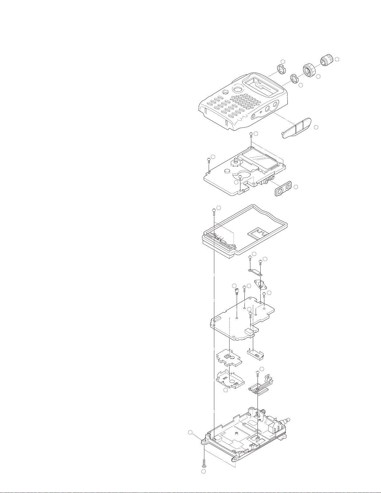
KNOB(PTT/MONI)
(K29-9108-13)
KEY TOP
(K29-9107-12)
WHIP ANTENNA
(T90-0781-05):K
(T90-0789-05):T,E
KNOB(ENC)
(K29-5159-03)
KNOB(VOL)
(K29-5150-03)
FRONT GLASS
(B10-2685-13):T,E
(B10-2723-13):K
CAP
(B09-0615-23)
CABINET ASSY
(A02-3620-13):T,E
(A02-3719-13):K
CONTENTS
DISASSEMBLY FOR REPAIR.................................................. 2
CIRCUIT DESCRIPTION .......................................................... 4
DESCRIPTION OF COMPONENTS....................................... 14
PARTS LIST............................................................................19
EXPLODED VIEW .................................................................. 32
PACKING ................................................................................ 33
ADJUSTMENT ........................................................................ 34
PC BOARD VIEWS
TX-RX UNIT (CONTROL SECTION) ...................................... 59
TX-RX UNIT ............................................................................ 65
TX-RX UNIT (VCO SECTION)................................................ 71
SCHEMATIC DIAGRAM ......................................................... 73
BLOCK DIAGRAM .................................................................. 81
LEVEL DIAGRAM ................................................................... 83
OPTIONS ................................................................................ 85
SPECIFICATIONS .................................................................. 86
TH-F6A/F7E
DISASSEMBLY FOR REPAIR
1. How to remove the case assembly from
the chassis:
1. Remove 2 screws (1).
2. Remove 2 knobs (2) and 2 round nuts (3).
3. Remove the SP/MIC jack cover (4).
4. Open the bottom part of case assembly and lift the front
panel from the chassis (5).
2. How to remove the main PCB:
2-1. Control section
1. Remove the SP/MIC jack cover (6).
2. Remove 5 screws (7) and lift and remove the control PCB
(TX-RX A/3).
3. Extract the encoder flat cable from the connector.
2-2. RF section
4. Remove 8 screws (8), and 1 round screw (9), then remove
the RF shield cover. Remove the soldering that connects
the whip antenna and bar-antenna (3 locations).
5. Remove the battery terminal screw (0).
6. Lift and remove the RF PCB (TX-RX B/3).
2-3. PLL/VCO section
7. Remove the soldering (8 locations) that holds the PLL/VCO
shield cover (!) then lift the shield cover.
8. Lift the PLL/VCO PCB upward to seperate it from the main
PCB.
3
2
3
4
7
7
7
8
8
8
6
2
9
8
8
8
10
11
5
2
1
Fig. 1
DISASSEMBLY FOR REPAIR
TH-F6A/F7E
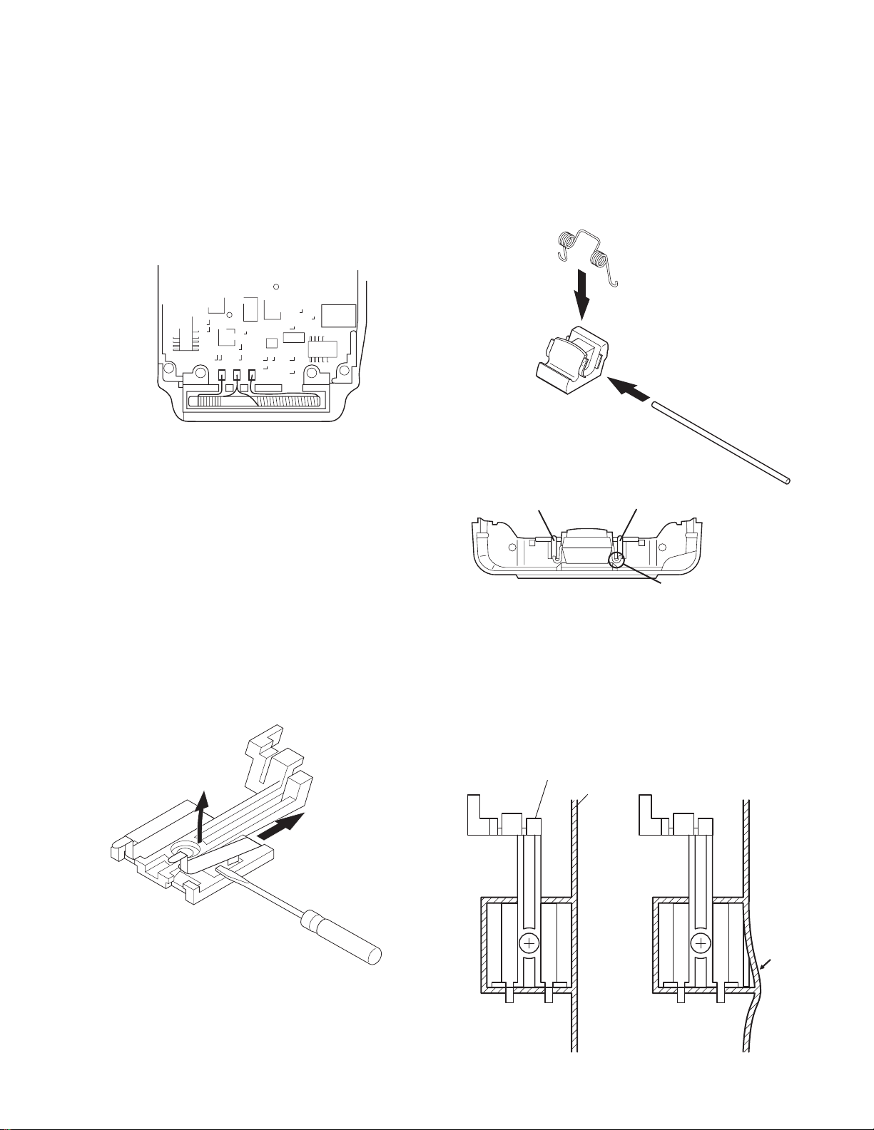
3. Soldering the Bar antenna wires
Before solding the bar antenna wires, form the wires as
shown in the figure 2.
Then solder the wires to lands on the PCB.
Fig. 2
5. Assembling a release latch
Place a coil spring(1) on the release latch(2) as shown in
the figure 4.
Then insert a shaft(3) into the release latch.
Push the above assembly into the rear panel while the
end of coil spring is hooked to the “A” tab.
1
2
Notch Notch
3
4. Removing a relay terminal
Insert a screw driver between the relay terminal and its
holder.
Then pull the relay terminal as shown in the figure 3.
A
Fig. 4
6. Caution at the time of reassembling
While you are reassembling the battery terminal holder
(J19-5428) and the packing (G53-1532), confirm that the
packing is reassembled at the condition that any swell is
not occurred on it. If the packing is assembled with any
swell, width of body also becomes expansive.
J19-5428
G53-1532
Swell not
allowed
Fig. 3
Fig. 5
3
TH-F6A/F7E
CIRCUIT DESCRIPTION
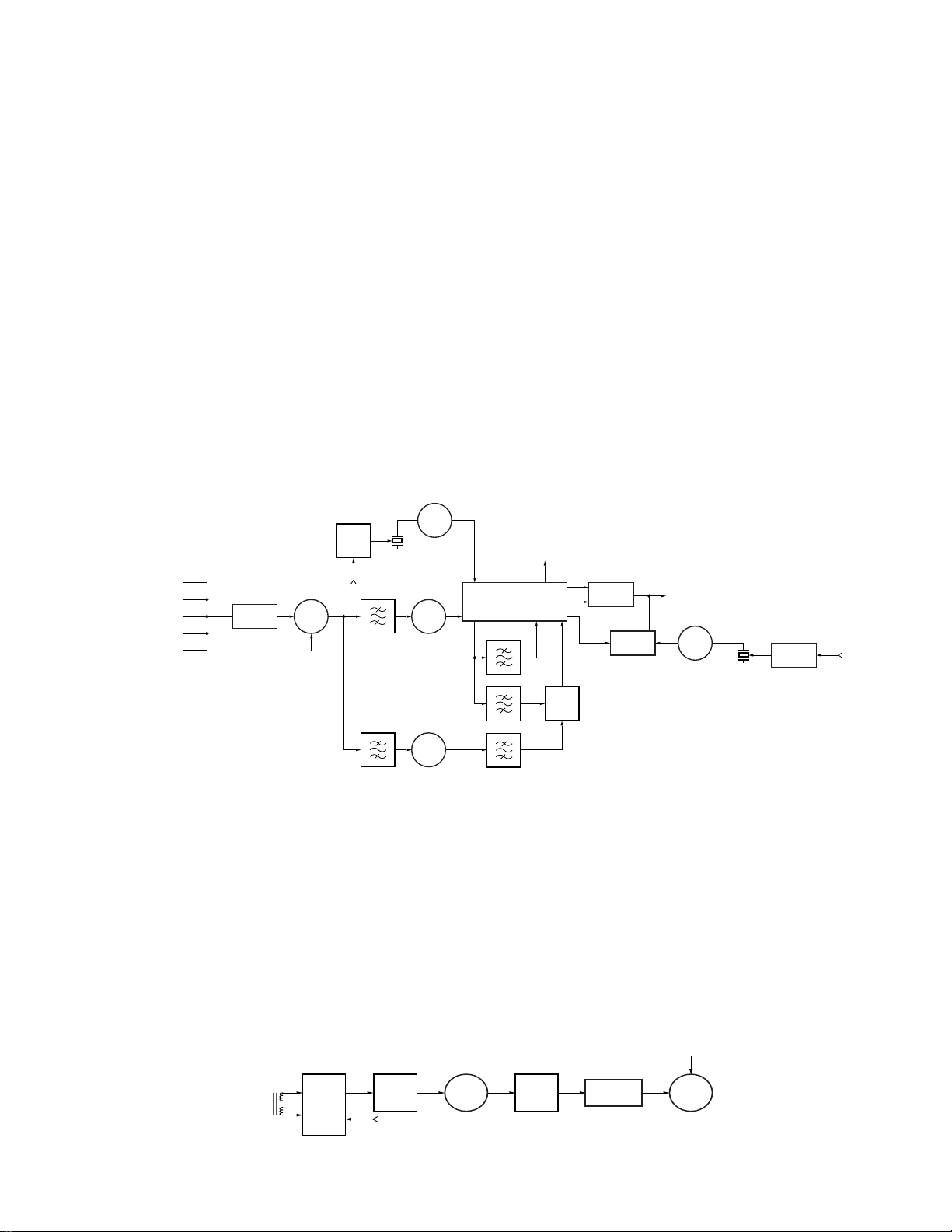
1. A band receiver system
1-1. Receiver circuit
The A band can receive signals in two bands: VHF (220 MHz
band <K type only>) and UHF (K type: three bands). It uses
FM receive mode only, and uses double conversion with the
first IF of 59.85 MHz and the second IF of 450 kHz.
The first amplifier is divided into two bands: 137 MHz -
173.995 MHz (216 MHz - 260 MHz <K type only>) and 410 MHz
- 470 MHz. The incoming signal from the antenna passes
through a low-pass filter and a duplexer, and goes to an
independent amplifier (Q63, Q62) for each band.
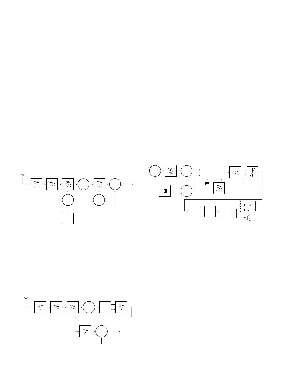
1-1-1. VHF band frontend
The incoming signal from the antenna passes through a
VHF band low-pass filter and a duplexer, passes through a
band-pass filter where it is tuned with varicaps (D76, D77),
and goes to the first amplifier (Q63). Unwanted signal
components are eliminated by a two-pole band-pass filter
where it is tuned by varicaps (D72, D75, D81, D83), and the
signal goes to the common mixer (Q45) for the A band. (K
type only: For 200MHz band reception, D74 is turned off with
a control signal to improve band-pass filter coupling and
ensure pass bandwidth.)
ANT
BPF
LPF
D76
D77
MPU
RFAMP BPFBPF
Q63
3SK320
APC&VTUNEA
D72,D75
D81,D83
MIX
Q45
MT6C
04AE
LO
1st IF
59.85MHz
1-1-3. Circuits following IF
The signal heterodowned to the first IF of 59.85 MHz by the
mixer (Q45) passes through a 15kHz MCF (XF2) and unwanted
signal components are eliminated. The resulting signal is
amplified by the IF amplifier (Q43) and goes to the FM IC (IC7).
The FM IC heterodowns it to the second IF of 450 kHz. Then,
the signal passes through a 15kHz external ceramic filter (CF4)
and goes to the FM IC again. The signal amplified by the IF
amplifier built into the IC is demodulated by the quadrature
FM demodulation circuit using a discriminator (CD1) and
converted into an audio signal and output.
The FM modulation signal output from the FM IC passes
through a low-pass filter consisting of a resistor and a capacitor
and is output to the control section. The demodulation signal
input to the control section goes to the electronic volume
(IC706, pin 13) to adjust the audio balance with the B band.
The output signal is amplified by the operational amplifier
(IC717), passes through an active filter consisting of Q719 and
Q717, and goes to the audio amplifier (IC707). The signal
amplified to a higher power by the audio amplifier becomes
the final output signal from the set and output through the
internal speaker or speaker output pin (J701).
19.8MHZ
IFAMPMCF
Q43
2SC
5108(Y)
X3
Q44
2SC
4915
AMP
IC717
4.50KHz
DE EMPHASIS
Q719
Q717
LPF
IC7
CF4
AUDIO
AMP
IC707
VR
IC700
BAF
J701
SP
MIX
Q45
MT6C
04AE
LO
XF2
TCXO
X1
Fig.1
1-1-2. UHF band frontend
The incoming signal from the antenna passes through a
UHF band low-pass filter and enters the first amplifier (Q62)
common to both A and B bands. The amplified signal is
distributed by L distributors (L95, L96) and goes to the LC filter
module (L92). Unwanted signal components are eliminated
by the filter, and the resulting signal passes through another
band-pass filter and enters the mixer (Q45).
ANT
BPF
LPF
HPF
RFAMP
3SK320
BPF
Q62
MIX
Q45
MT6C
04AE
L95
L96
LO
LC FILTER
MODULE
1st IF
59.85MHz
Fig.2
4
L92
Fig.3
1-2. Mixer local oscillator
1-2-1. First mixer
The local oscillator signal for the first mixer is supplied from
the VCO-PLL circuit.
1-2-2. Second mixer
The local oscillator signal for the second mixer is a 59.4
MHz signal that is produced by multiplying the 19.8MHz TCXO
(X1) oscillator output with a multiplier (Q44).
2. B band receiver system
2-1. Receiver circuit
The B band has a broadband receiver circuit configuration
and implements broadband reception of 100 kHz to 1.3 GHz.
FM/AM/SSB/CW reception is possible in the range 100 kHz to
29.7 MHz, and FM/wide FM/AM/SSB/CW reception is possible
in the range 29.7 MHz to 1.3 GHz. The FM/AM receiver circuit
uses double conversion with the first IF of 57.6 MHz and the
second IF of 450 kHz. The SSB/CW receiver circuit uses triple
conversion with the first IF of 57.6 MHz and the second IF of
450 kHz. The wide FM receiver circuit uses single conversion
with the IF of 10.8 MHz.
CIRCUIT DESCRIPTION
TH-F6A/F7E
The first amplifier is divided into four bands: 100 kHz - 50
MHz, 50MHz - 108MHz, 108 MHz - 265 MHz, 265 MHz - 600
MHz, and 600 MHz - 1.3 GHz. The incoming signal from the
antenna passes through a low-pass filter and a duplexer, and
goes to an independent amplifier for each band. Then, the
signal goes to the second common broadband amplifier (IC10)
and its output is fed to the mixer (Q28) and heterodowned to
the first IF.
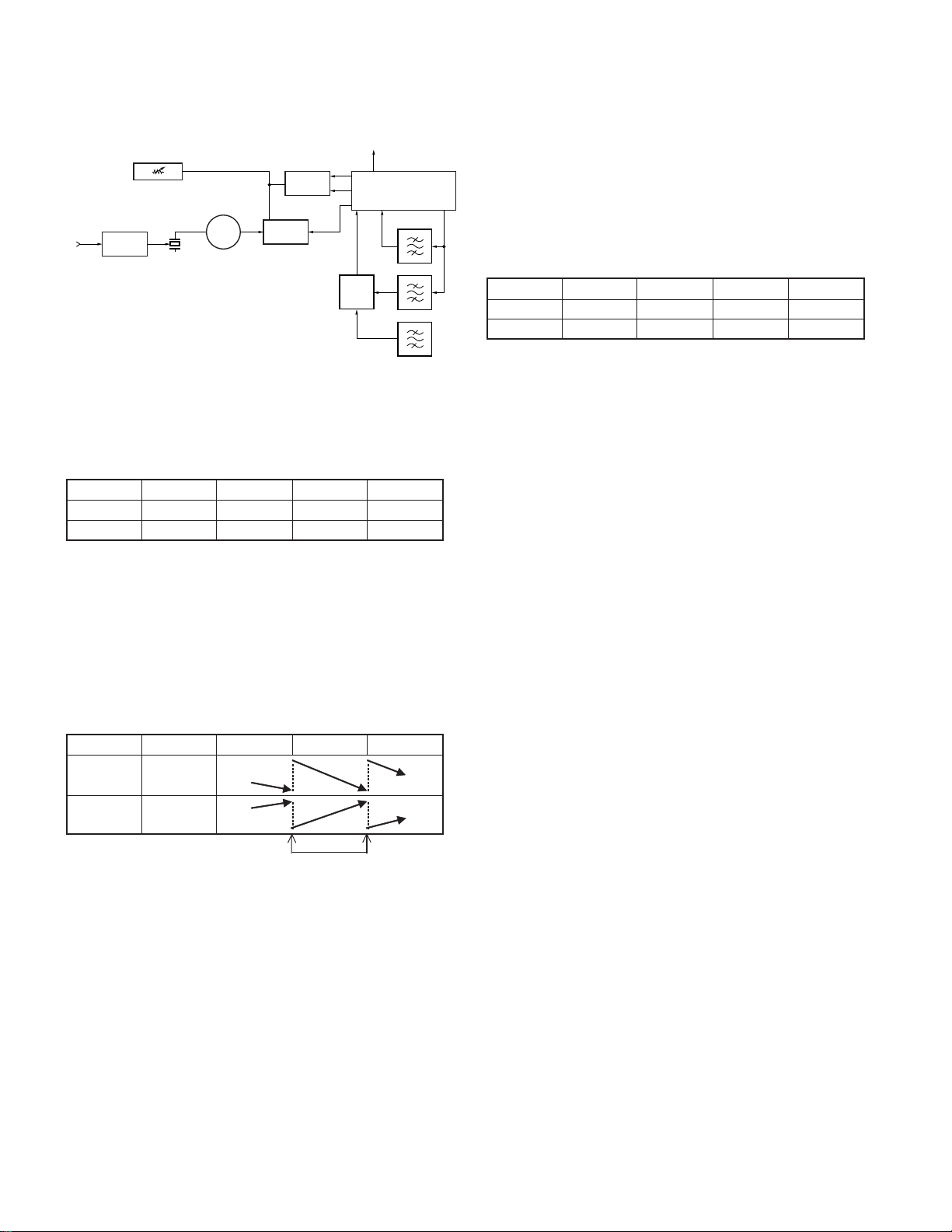
2-1-1. FM/AM receiver circuit
The signal heterodowned to the first IF of 57.6MHz passes
through a 15kHz MCF (XF1), and unwanted signal components
are eliminated. The resulting signal is amplified by the IF
amplifier (Q26) and goes to the FM IC (IC5). The FM IC
heterodowns it to the second IF of 450 kHz. In FM mode, the
signal passes through a 12.0kHz external ceramic filter (CF3)
and goes to the FM IC. The signal amplified by the internal IF
amplifier is demodulated by the quadrature FM demodulation
circuit using a coil (L19) and converted into an audio signal
and output. In AM mode, the signal passes through a 4kHz
external ceramic filter CF1 and goes back to the FM IC. It is
amplified by the AM AGC amplifier built in the FM IC, an audio
Q27
2SC
4915
OSCILLATOR
IF AMP
Q26
2SC
4915
Q24
2SC
4915
450KHz
UHF(600~1300)
UHF(265~600)
VHF(108~265)
TUNE
D29
HVC
376B
19.05MHZ
FINE1
AMP
IC10
HF
HF
MPC2746TB
MIX
Q28
MT6C
03AE
LO
MCF
57.6MHz
XF1
CF5
10.8MHz
output from the FM IC as an audio signal.
2-1-4. AM bar antenna receiver circuit
This unit incorporates an AM bar antenna, and either the
bar antenna or the supplied antenna can be selected in the
520kHz-1.8MHz (SW) and 3.5MHz-10.1MHz (MW) bands (the
initial value: bar antenna). The bar antenna has two kinds of
tuners for SW and MW tuning, one of which is selected with a
switching FET (Q32, Q48, Q52). The antenna is tuned with a
varicap (D60) for AM tuning to select a desired signal. The
signal from the bar antenna is amplified by and its impedance
is converted by the buffer amplifier (Q59), and the resulting
signal goes to the common mixer (Q28) for the B band. The
signal is routed over the same path for AM demodulation as
for the supplied antenna after leaving the mixer.
TUNE
D60
KV1566J
Q6,Q4
RF AMP
3SK320
BAR
ANT
SW
Q48,52
2SK1824
Q32
2SK1830
Q59
signal demodulated by the diode detection circuit is output.
2-1-2. SSB/CW receiver circuit
In SSB/CW mode reception, the signal takes the same path
to CF1 as in AM mode. The signal input to the FM IC again is
amplified by the AM AGC amplifier in the FM IC, then output
from the AM IF output pin. The signal is fed to the third mixer
(IC4) and converted to an audio signal and output.
2-1-3. Wide FM receiver circuit
The signal converted to the first IF of 10.8 MHz passes
through a ceramic filter CF5 for wide FM, and is amplified by
the IF amplifier (Q24). The signal passes through ceramic filter
CF2 again to eliminate unwanted signal components, and goes
to the FM IF input (pin 7) of the FM IC. The input signal is
amplified by the IF amplifier in the IC, demodulated by the
quadrature FM demodulation circuit using an L18 coil, and
SMB
SQB
SW
FM
Q22,29
D25
DAN
235E
SW
AM
SSB/CW
UPA672T
SSB DET
IC4
TA4101F
OSCILLATOR
Q23
LMX
2N
453KHz
TUNE
D20,24
KV1566J
IC5
TK10931V
CF1
CF3
CF2
10.8MHz
Fig.4
2-1-5. Audio signal
The FM and AM demodulation signals output from the FM
IC (IC5) pass through a low-pass filter consisting of a resistor
and a capacitor, and goes to the switching FET (Q29), from
which a switched signal is output to the control unit. The
SSB/CW demodulation signal passes through an RC LPF,
connects to the Q29 output section, and output to the control
unit through a line common to all modes. The demodulation
signal input to the control unit goes to the electronic volume
(IC706, pin 16), the audio balance output with the A band is
restricted, then the signal is output. It joins the A band
demodulation signal and is processed in the same manner
for both A and B bands.
LO
SW
D57
HSC277
AMP
IC10
MPC2746TB
MIX
Q28
MT6C
03AE
FINE2
Fig.5
5
TH-F6A/F7E
CIRCUIT DESCRIPTION
SMB
SQB
FM
AM
SW
D25
DAN
235E
10.8MHz
FINE2
TUNE
D20,24
KV1566J
IC706
M62364
FP
453KHz
OSCILLATOR
Q23
LMX
2N
Fig.6
SSB DET
IC4
TA4101F
SW
Q22,29
UPA672T
SSB/CW
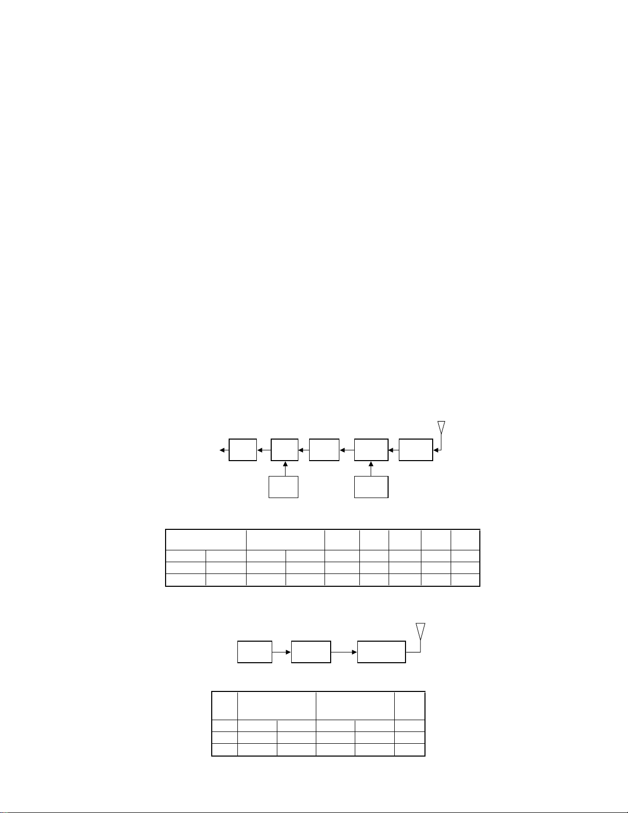
2-2. Mixer local oscillator
2-2-1. First mixer
The local oscillator signal for the first mixer is supplied from
the VCO-PLL circuit. To offset according to modes, the PLL
switching frequency changes in FM/AM/CW, USB, LSB.
1st LOCAL (PLL Switching Frequency)
FM/AM CW USB LSB
UPPER Per 5kHz FM-2.5kHz FM-4.5kHz FM-0.5kHz
LOWER Per 5kHz FM-2.5kHz FM-4.5kHz FM-0.5kHz
* PLL Switching Frequency changes with the modes.
Table.1
2-2-2. Second mixer
The local oscillator signal of the second mixer uses
57.15MHz which is three times as high as the 19.05MHz crystal
oscillator (X3) output. This local oscillator signal is used to (i)
implement fine steps during fine tuning and (ii) offset during
SSB/CW reception.
2rd LOCAL (Oscillator Frequency)
FM/AM
UPPER 57.15MHz
LOWER 57.15MHz
* During fine tuning, it changes with 33.3 Hz step from PLL
Switching Frequency to the next Switching Frequency.
(i) Fine tuning function
When the fine tuning function is ON, the PLL comparison
frequency is 5 kHz (5kHz step). The "receive frequency of
10Hz steps as a set" is implemented by operating the local
oscillator signal of the second mixer in 33.3Hz steps in the
5kHz frequency range. The frequency is varied by 57.15
MHz +/- 2.5 kHz by changing the voltage applied to the
varicap (D29) installed in the local oscillator circuit.
(ii) Mode offset
The IF frequency is adjusted by 2 Hz in SSB mode so that
the demodulated signal passes through the center of the
4kHz ceramic filter (CF1). The frequency is adjusted by
varying the local oscillator frequency.
6
CW(Fine Tuning)
57.15MHz+2.5kHz
Oscillator Frequency
Oscillator Frequency
57.15MHz-2.5kHz
USB(Fine Tuning) LSB(Fine Tuning)
PLL Switching Frequency
Table.2
57.15MHz-2.5kHz
57.15MHz+2.5kHz
IC5
TK10931V
2-2-3. Third mixer
The third mixer (IC4) works in SSB/CW mode only. The
local oscillator signal of 450 kHz +/- 2 kHz is produced in SSB
mode to restore 2kHz correction (offset), and the signal of 450
CF1
CF3
kHz - 800 Hz is produced to generate an 800Hz beat frequency
in CW mode. A demodulation signal is produced in SSB, and
a 800Hz beat signal is produced in CW.
450KHz
3rd LOCAL (Oscillator Frequency)
FM/AM CW USB LSB
CF2
UPPER 450kHz
LOWER 450kHz
450kHz+800Hz 450kHz+2kHz 450kHz-2kHz
450kHz+800Hz 450kHz-2kHz 450kHz+2kHz
* Perform Mode OFFSET
Table.3
2-3. AGC circuit
The AGC is controlled by using the output from the RF AGC
built into the FM IC (IC5). The AGC is controlled by controlling
the bias current of the IF amplifier (Q26) and the forward
current of the pin diode (D32) for the attenuater. In non-FM
mode, the AM AGC circuit built-into the FM IC is also used.
3. Control
3-1. Reset and backup circuits
The CPU reset signal is generated with the CR time constant
by detecting a rising edge of the M4 line voltage with the
voltage detection IC (IC709). If the voltage supplied to the THF6/TH-F7 decreases and the M4 line voltage falls below the
detection voltage of the voltage detection IC (IC710), the CPU
(IC705) detects it through the interrupt pin, backs up data in
the EEPROM (IC704), and shuts the power off.
3-2. Voltage detection processing
The voltages are measured through the A/D port of the CPU
(IC705) for processing. The battery voltage is supplied through
a resistor, and a warning sound is produced when an abnormal
power supply voltage (17.5 to 22.0 V) is applied to the battery
meter during transmission. The squelch voltage is input from
the IF IC, and a change in the noise voltage is detected to
control squelch. The S meter voltage is input from the IF IC to
control the S meter display. Thermistor voltage (temperature)
detection, remote control microphone key operation, VOX
voltage monitoring, and TONE/DCS decoding are performed
through the A/D port.
3-3. VOX
The signal output from the microphone amplifier (IC702) is
amplified by Q701, rectified/integrated by D709 to convert to
DC voltage, and monitored through the A/D port of the CPU
(IC705) to perform VOX processing.
3-4. Battery save
The CPU (IC705) controls Q728 through the SAVE port to
save battery power.
3-5. LED drive circuit
The CPU (IC705) controls Q709 to turn LEDs on to illuminate
the LCD and keys. The ON AIR/BUSY LED is directly controlled
through the open drain port of the CPU (IC705).
CIRCUIT DESCRIPTION
TH-F6A/F7E
3-6. Key/encoder input circuit
The PWR key is assigned to an interrupt port. The PTT key
is assigned to another interrupt port. The other keys and
destination diodes form a 5x6 matrix and pressing a key is
detected by scanning the matrix by software. The encoder
reads data through the interrupt port.
3-7. CTCSS/DCS
The encode signal is output from the D/A port of the CPU
(IC705) by software. The signal level is adjusted with an
electronic VR (IC706) and the signal is divided into VCO and
TCXO and modulated like a 9600bps packet signal.
The audio signal from the IF IC passes through the IC712/
IC711 waveform rectification circuit and enters the A/D port
of the CPU (IC705). The CPU detects that the specified CTCSS
tone frequency and DCS code are detected and controls
muting.
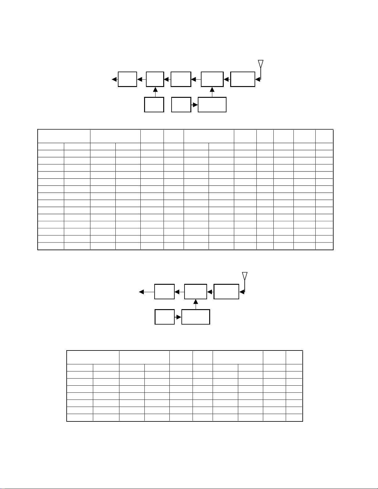
4. PLL • VCO
The TH-F6/TH-F7 has two PLL loops and a total of four VCOs,
two for each PLL loop. The PLL is divided for A band reception,
B band reception and transmission. Each VCO has oscillator
frequency shift control. For relationships between VCO
oscillator frequencies and shifts, see Table 4-11.
3-8. DTMF
The DTMF signal is output from the D/A port of the CPU
(IC705) by software means. The signal is mixed with a signal
at the input side of the audio amplifier (IC707) and output as a
monitor tone. It is mixed with a modulation signal at the input
side of the preemphasis (IC701) and used to as a transmit
signal.
3-9. Serial control
The REM/PTT terminal of the speaker mic jack (J701) is
switched by the CPU (IC705) and functions as TXT/RXD to
communicate with a personal computer.
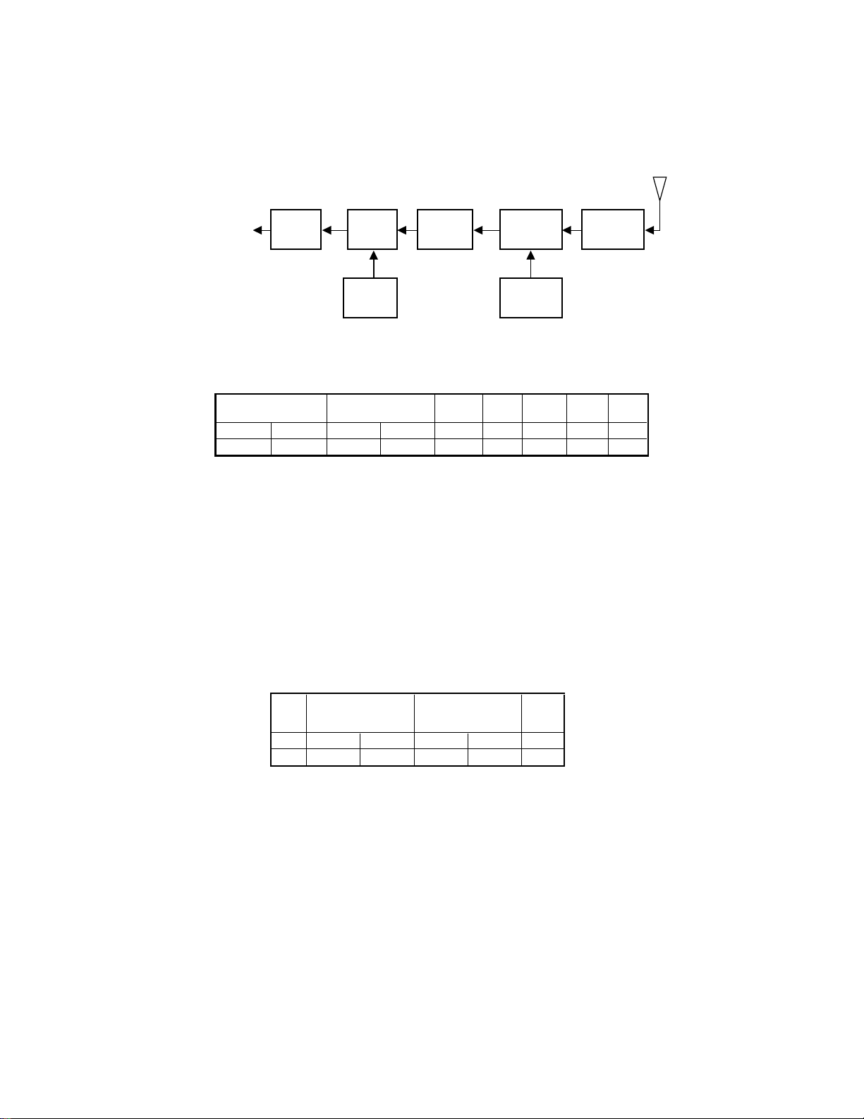
TH-F6A Frequency Construction
A band RX Double Super Heterodyne
Audio
RX Freq. Range
[MHz]
137.000 173.995 196.850 233.845 Upper 59.85 59.4 Lower 450
216.000 259.995 275.850 319.845 Upper 59.85 59.4 Lower 450
410.000 469.995 350.150 410.145 Lower 59.85 59.4 Lower 450
TH-F6A Frequency Construction
TX
2nd
Mixer
1st IF Amplifier1st Mixer2nd IF
VCO2nd LO
Fig.7
1st IF
VCO Oscillation
[MHz]
1st Mix.
[MHz]
2nd LO
[MHz]
Table.4
VCO Devider Amplifier
Fig.8
Transmission
Frequency Range
Band
[MHz]
[MHz] Devide
144 144.000 147.995 576.000 591.980 4
220 222.000 224.995 444.000 449.990 2
440 438.000 449.995 438.000 449.995 1
VCO Oscillation
[MHz]
2nd
Mix.
2nd IF
[kHz]
Table.5
7
TH-F6A/F7E
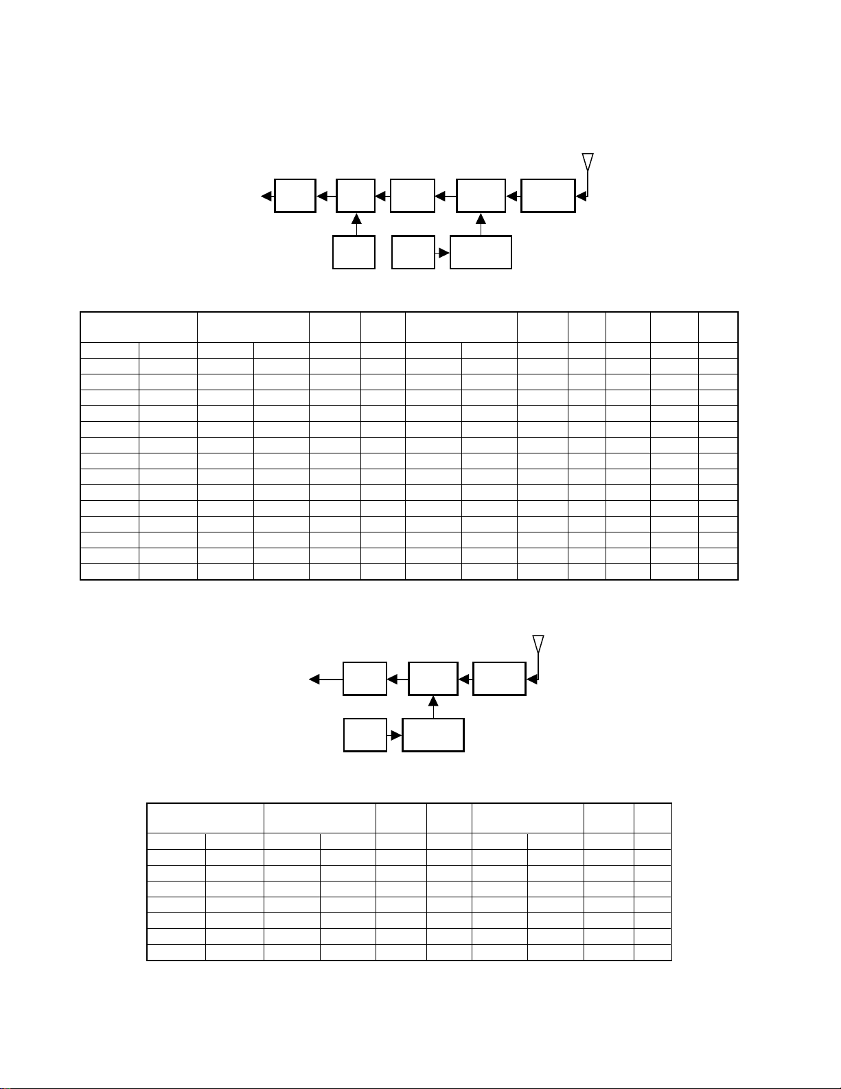
* TH-F6A Frequency Construction
B band RX FM mode Double Super Heterodyne
CIRCUIT DESCRIPTION
Audio
2nd IF
2nd
Mixer
2nd LO VCO
1st IF
1st
Mixer
Devider
Multiplyer
Amplifier
Fig.9
1st IF
RX Freq. Range [MHz] VCO Oscillation [MHz] 1st LO
0.100 22.995 461.600 644.760 1 8 57.700 80.595 Upper 57.6 57.15 Lower 450
23.000 103.995 322.400 646.380 1 4 80.600 161.595 Upper 57.6 57.15 Lower 450
104.000 266.995 323.200 649.190 1 2 161.600 324.595 Upper 57.6 57.15 Lower 450
267.000 409.995 324.600 467.595 1 1 324.600 467.595 Upper 57.6 57.15 Lower 450
410.000 469.995 352.400 412.395 1 1 352.400 412.395 Lower 57.6 57.15 Lower 450
470.000 591.995 527.600 649.595 1 1 527.600 649.595 Upper 57.6 57.15 Lower 450
592.000 706.995 534.400 649.395 1 1 534.400 649.395 Lower 57.6 57.15 Lower 450
707.000 707.995 382.300 382.798 2 1 764.600 765.595 Upper 57.6 57.15 Lower 450
708.000 851.995 325.200 397.198 2 1 650.400 794.395 Lower 57.6 57.15 Lower 450
852.000 868.995 454.800 463.298 2 1 909.600 926.595 Upper 57.6 57.15 Lower 450
869.000 896.995 405.700 419.698 2 1 811.400 839.395 Lower 57.6 57.15 Lower 450
897.000 922.995 477.300 490.298 2 1 954.600 980.595 Upper 57.6 57.15 Lower 450
923.000 938.995 432.700 440.698 2 1 865.400 881.395 Lower 57.6 57.15 Lower 450
939.000 1009.995 498.300 533.798 2 1 996.600 1067.595 Upper 57.6 57.15 Lower 450
1010.000 1299.995 476.200 621.198 2 1 952.400 1242.395 Lower 57.6 57.15 Lower 450
Multiply Devide 1st Mix.
[MHz]
2nd LO
[MHz] 2nd Mix.
2nd IF
[kHz]
B band RX WFM mode Single Super Heterodyne
Audio
RX Freq. Range [MHz] VCO Oscillation [MHz] 1st LO
29.700 54.995 324.000 526.360 1 8 40.500 65.795 Upper 10.8
55.000 91.995 353.600 649.560 1 8 44.200 81.195 Lower 10.8
92.000 130.795 324.800 479.980 1 4 81.200 119.995 Lower 10.8
130.800 150.995 566.400 647.180 1 4 141.600 161.795 Upper 10.8
151.000 309.995 323.600 641.590 1 2 161.800 320.795 Upper 10.8
310.000 449.995 320.800 460.795 1 1 320.800 460.795 Upper 10.8
450.000 659.995 439.200 649.195 1 1 439.200 649.195 Lower 10.8
660.000 1299.995 324.600 644.598 2 1 649.200 1289.195 Lower 10.8
Table.6
1st IF
VCO
1st
Mixer
Devider
Multiplyer
Amplifier
Fig.10
Multiply Devide 1st Mix.
Table.7
1st IF
[MHz]
8
* TH-F7 Frequency Construction
A band RX Double Super Heterodyne
TH-F6A/F7E
CIRCUIT DESCRIPTION
Audio
RX Freq. Range
[MHz]
144.000 145.995 203.850 205.845 Upper 59.85 59.4 Lower 450
430.000 439.995 370.150 380.145 Lower 59.85 59.4 Lower 450
TH-F7 Frequency Construction
2nd
Mixer
VCO Oscillation
[MHz]
1st IF Amplifier1st Mixer2nd IF
Fig.11
1st Mix.
Table.8
1st IF
[MHz]
VCO2nd LO
2nd LO
[MHz]
2nd
Mix.
2nd IF
[kHz]
Fig.12
Transmission
Band
Frequency Range
[MHz] Devide
[MHz]
144 144.000 145.995 576.000 583.980 4
440 430.000 439.995 430.000 439.995 1
VCO Oscillation
[MHz]
Table.9
9
TH-F6A/F7E
* TH-F7 Frequency Construction
B band RX FM mode Double Super Heterodyne
CIRCUIT DESCRIPTION
Audio
2nd IF
2nd
Mixer
2nd LO VCO
1st IF
1st
Mixer
Devider
Multiplyer
Amplifier
Fig.13
1st IF
RX Freq. Range [MHz] VCO Oscillation [MHz] 1st LO
0.100 22.995 461.600 644.760 1 8 57.700 80.595 Upper 57.6 57.15 Lower 450
23.000 103.995 322.400 646.380 1 4 80.600 161.595 Upper 57.6 57.15 Lower 450
104.000 266.995 323.200 649.190 1 2 161.600 324.595 Upper 57.6 57.15 Lower 450
267.000 409.995 324.600 467.595 1 1 324.600 467.595 Upper 57.6 57.15 Lower 450
410.000 469.995 352.400 412.395 1 1 352.400 412.395 Lower 57.6 57.15 Lower 450
470.000 591.995 527.600 649.595 1 1 527.600 649.595 Upper 57.6 57.15 Lower 450
592.000 706.995 534.400 649.395 1 1 534.400 649.395 Lower 57.6 57.15 Lower 450
707.000 707.995 382.300 382.798 2 1 764.600 765.595 Upper 57.6 57.15 Lower 450
708.000 851.995 325.200 397.198 2 1 650.400 794.395 Lower 57.6 57.15 Lower 450
852.000 868.995 454.800 463.298 2 1 909.600 926.595 Upper 57.6 57.15 Lower 450
869.000 896.995 405.700 419.698 2 1 811.400 839.395 Lower 57.6 57.15 Lower 450
897.000 922.995 477.300 490.298 2 1 954.600 980.595 Upper 57.6 57.15 Lower 450
923.000 938.995 432.700 440.698 2 1 865.400 881.395 Lower 57.6 57.15 Lower 450
939.000 1009.995 498.300 533.798 2 1 996.600 1067.595 Upper 57.6 57.15 Lower 450
1010.000 1299.995 476.200 621.198 2 1 952.400 1242.395 Lower 57.6 57.15 Lower 450
Multiply Devide 1st Mix.
[MHz]
2nd LO
[MHz] 2nd Mix.
2nd IF
[kHz]
B band RX WFM mode Single Super Heterodyne
Audio
RX Freq. Range [MHz] VCO Oscillation [MHz] 1st LO
29.700 54.995 324.000 526.360 1 8 40.500 65.795 Upper 10.8
55.000 91.995 353.600 649.560 1 8 44.200 81.195 Lower 10.8
92.000 130.795 324.800 479.980 1 4 81.200 119.995 Lower 10.8
130.800 150.995 566.400 647.180 1 4 141.600 161.795 Upper 10.8
151.000 309.995 323.600 641.590 1 2 161.800 320.795 Upper 10.8
310.000 449.995 320.800 460.795 1 1 320.800 460.795 Upper 10.8
450.000 659.995 439.200 649.195 1 1 439.200 649.195 Lower 10.8
660.000 1299.995 324.600 644.598 2 1 649.200 1289.195 Lower 10.8
Table.10
1st IF
VCO
1st
Mixer
Devider
Multiplyer
Amplifier
Fig.14
Multiply Devide 1st Mix.
Table.11
1st IF
[MHz]
10
CIRCUIT DESCRIPTION
TH-F6A/F7E
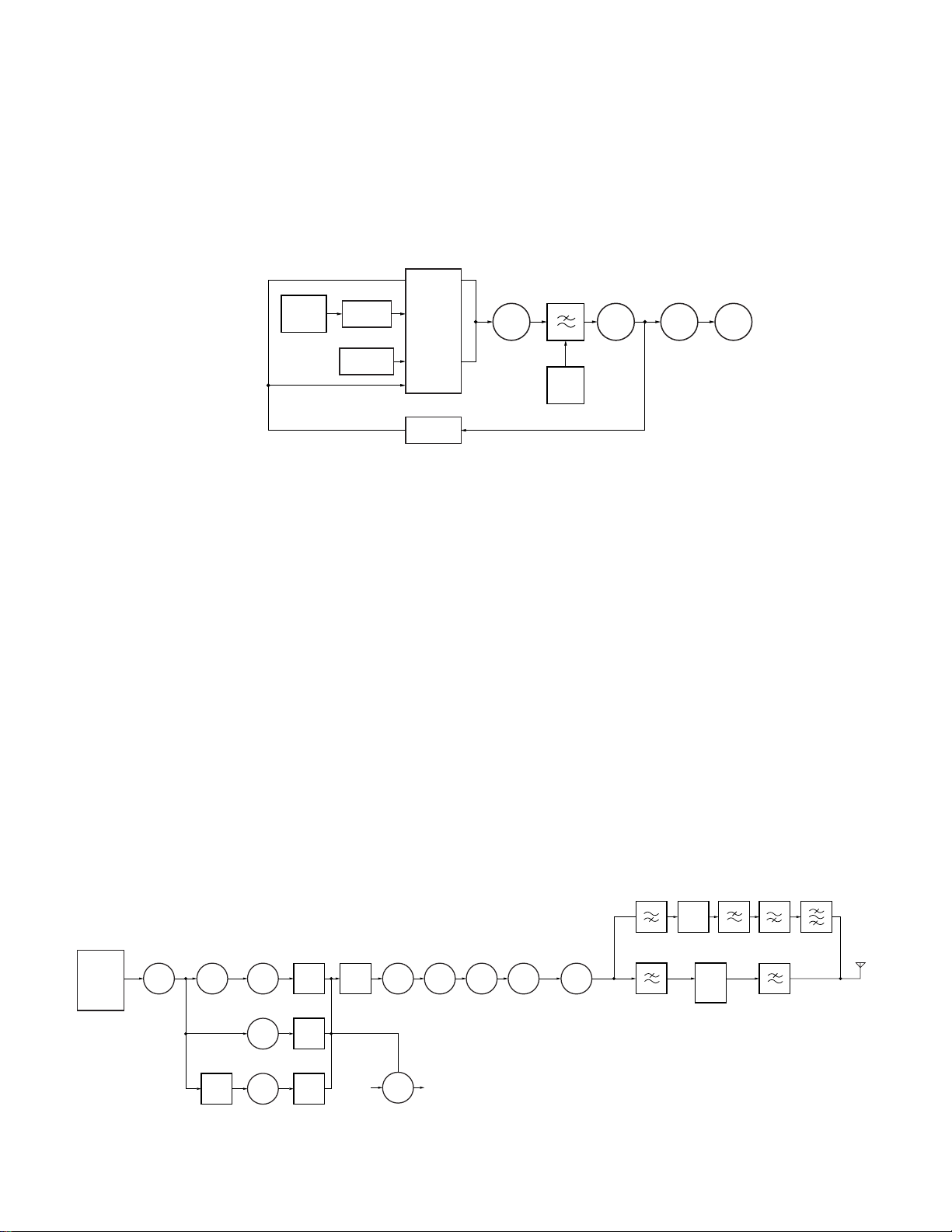
4-1. A band reception
IC6 functions as A band reception PLL. This PLL IC controls
the VCO produced by Q34. VCOs are changed over by
switching the power provided to each VCO by Q35 through
control line "DAVCOS" from the CPU. VCO power passes
through a ripple filter consisting of Q31 and C235.
VCO
RIPPLE FILTER
Q31
2SC4617(S)
Q38
MA2S111
SW
Q35
HNIJ02FU
SHIFT SW
Q70 2SJ243
Q69 DTC144EE
A
Q34
MT6C03AE
D35,37
1SV305
D36,34
MA25304
D40
HVC131
PLL
IC6
LMX2326TMX
4-2. B band reception and transmission
IC2 functions as B band reception PLL. This PLL IC controls
the VCO produced by Q9. VCOs are changed over by switching
the power supplied to each VCO by Q10 through control line
"DBSS" from the CPU. VCO power passes through a ripple
filter consisting of Q7 and C52. Each VCO output is amplified
by a common amplifier (Q13).
4-2-1. 0.1MHz-267MHz reception, VHF (220MHz <K type
only>) band transmission
The VCO oscillator frequency is UHF. The signal output
from Q13 goes to the prescaler IC (IC3) and is divided into 1/8
(0.1MHz-23MHz), 1/4 (23MHz-104MHz), and 1/2 (104MHz267MHz). Division is controlled by using control signals "SW1
(Q15)" and "SW2 (Q15)" from the CPU. The division output is
amplified by an amplifier (Q19), and the signal goes to the
mixer (Q28) during reception and to the drive during
transmission. The PLL IC FIN input is generated by extracting
the output from Q13 and amplifying it with an amplifier (Q11).
VCO
B
Q2MT6C03AE
D18 HVC131
D11,12
HVC3758
D21 HVC131
D10,16
HVC3758
AMP
Q13
2SC
5108(Y)
AMP
Q12
2SC
5009
DEVIDER
IC3
UPB
1509GV
AMP
Q21
2SC
5009
AMP
Q93
MT6C
03AE
AMP
Q19
2SC
5009
D99
HSC
D100
HSC
D101
HSC
SW
SW
AMP AMP
Q71
(R24)
Q28
MT6C
03AE
Q72
2SC
5192
Lo
MIX
D102
2SC4226
HSC
277
277
277
277
Each VCO output is amplified by a common amplifier Q37.
In VHF/UHF band reception, the signal passes through a lowpass filter, is amplified by Q40, then by a common local
amplifier (Q41), and goes to a mixer. This low-pass filter uses
a varicap (D28, D106) to shift cut-off frequency. The FIN input
to the PLL IC is taken from the Q40 output.
AMP
Q37
2SC
5108(Y)
LPF
TUNE
D28,106
HVC375B
AMP
Q40
2SC
5009
AMP
Q41
2SC
5009
MIX
Q45
MT6C
04AE
Fig.15
4-2-2. 267MHz-707MHz reception, UHF transmission
The Q13 output goes to the mixer during reception and to
the drive during transmission. The PLL IC FIN input is
generated by extracting the output from Q13 and amplifying
it with an amplifier (Q11).
4-2-3. 707MHz-1.3GHz reception
Output signal from Q13 is amplified by an aplifier(Q11), then
the signal is multiplied by 2 by a multiplier (Q12). The signal
is then amplified with three amplifiers (Q21), and goes to the
mixer (Q28) during reception and to the drive (Q71) during
transmission. The FIN input of the PLL IC (IC2) is input by
taking the output from Q11.
DRIVE AMP DRIVE AMP
Q54
Q56
2SK
2SK
2973
2973
RF POWER AMP
Q55
2SK
3476
UHF
VHF
HPF HPFSW
HVC131
LPF
D53
D54
SW
D49 D85
D50 D86
D51
D52
HVC131
LPF
LPF
BPF
ANT
Fig.16
11
TH-F6A/F7E
CIRCUIT DESCRIPTION
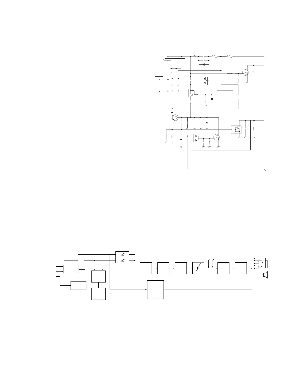
5. Lithium ion battery charging control
If a lithium ion battery is installed, it is charged when power
is supplied to the DCIN JACK from outside. The mechanism
of charging control is described below.
When power is provided to the DCIN JACK, Q65 turns ON
and the control port is made LOW to notify the CPU of
connection of an external power source. The CPU grounds
the Q2 collector according to this information. As a result, Q5
turns OFF and Q1 turns ON. If the remaining battery level is
low, the Q1 collector current increases, so the emitter voltage
is reduced by R2 and Q2 turns ON to charge the battery
(charging). The CPU pulls up the Q2 collector voltage, uses
this port as input, and monitors it. If the battery voltage level
increases, the Q1 collector current decreases, the emitter
voltage drops and Q2 turns OFF at a certain voltage. The CPU
recognizes that charging is approaching its end by this change,
and enters an additional charging state. In the additional
charging state, the CPU grounds the Q2 collector and
continues charging slowly in about an hour. When it ends,
the battery charging is complete.
IC1 is a lithium ion battery charge control IC. When the
battery voltage exceeds 8.4 V, the output port is made HIGH
and Q3 is turned OFF to stop charging. If it is 8.4 V or lower,
"LOW" is output and Q3 is turned ON to bias Q1.
J1
Q1
2SD1760
CN1
CN2
CHG
10
R19
C4 100p
C3 100p
C5 1000p
D2 RB051L-40
10
R2
C21 1000p
C2
1000p
C15 0.1u
C23 1000p
C24 100p
D6
RB051L-40
D7 DA221
Q3
DTA143ZE
470p
C17
C18
F2
4A
C19
39k
R7
D4
HZU2ALL
470k
470p
R10
L3
470p
C22
1.2k
R5
0.1u
R6
100k
C16
D5
15S361
IC1
LM3420-8.4
OUT + IN
5
0.1u
COMP NC
4
Q5
2SK1830
F1
2.5A
R23 22k
GND
Q2
DTC123JE
1
2
3
Q65
2SK3019
R24 4.7k
B
DCDET
C46
0.01u
CHG1
C20
0.01u
R365 1.0M
VTx
Fig.17
6. Receive audio circuit
The receive signal demodulated by the FM IC on each of
the A and B bands passes through an electronic volume (IC706)
and is amplified by IC717. The signal is deemphasized by
Q719, passes through a variable RESISTOR (AFVR), is
amplified by the audio amplifier (IC707), and output to the
speaker (SP1) or external speaker jack (J701).
CTCSS or DCS is a 2-channel multiplexer from FM IC output,
and A or B band is selected, the signal passes through an
amplifier filter (IC711), and goes to the CPU where it is
decoded.
TK10931V
IC5
FM
AM
SSB/CW
IF DET
IC7
TA31136FN
SW
Q22,29
UPA672T
SSB DET
TA4101F
IC706
M62364 FP
SW
IC712
TC4W53FU
IC4
IC711
TA75W01FU
TONE FILTER
TONEIN
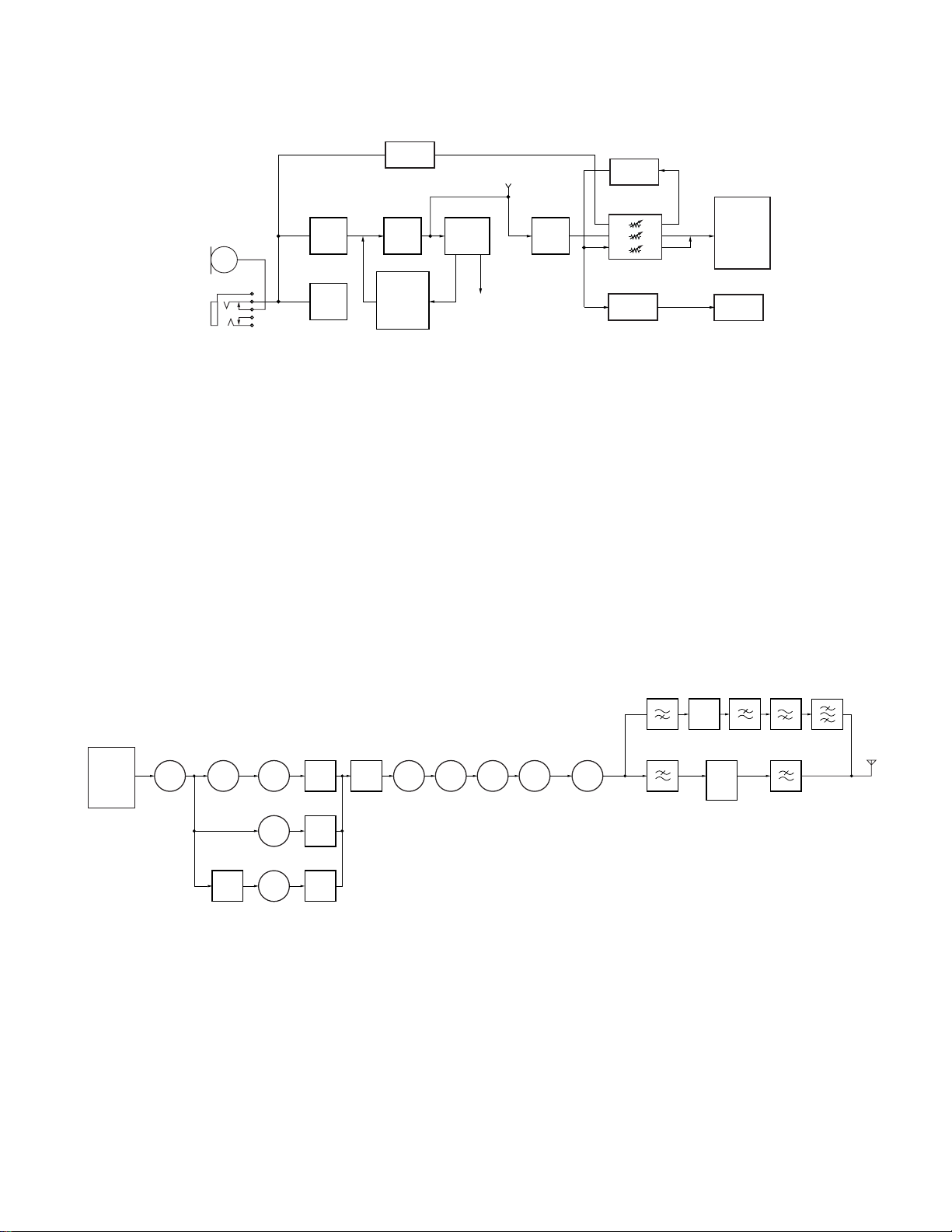
7. Transmission signal system
7-1. Modulation circuit
The audio modulation input is switched between external
input and internal microphone using an external microphone
terminal, and its base band is processed by microphone
amplifier IC 702 and preemphasis/limiter IC 701. The signal is
mixed with a DTMF subtone before the preemphasis circuit,
the level is adjusted by electronic VR IC706, and the signal is
input to the VCO as a modulation signal. The excessive input
of the 9600bps packet signal and the high-speed FM mode
12
The 9600bps packet signal is produced by converting the
impedance of the output signal from the FM IC by Q720 and
Q721, passing it through the Q722 switch, and outputting it to
the speaker (SP1) or external speaker jack (J701).
AMP
IC717
TC75
S51F
DE EMPHASIS
Q720
2SC4617(R)
Q721
2SJ347
Q722
2SK1830
SW
Q719
2SC4617
(R)
MUTE SW
Q704
2SJ
347
AF VR
BEEPDTMF
AUDIO AMP
IC707
TA73
68F
MUTE SW
Q706
2SK1588
Q708
2SK1830
Fig.18
SSTV transmit signal input through the external microphone
input terminal is suppressed by D710 and D711, switched by
IC703, and input to electronic VR IC706. The level-adjusted
signal is amplified by Q719, passes through electronic VR
IC706, and is divided into two paths: one for modulating the
VCO through electronic VR IC706 the other for modulating
TCXO X1 through amplifier IC702 to perform broadband
transmission modulation.
SP
SP
CIRCUIT DESCRIPTION
SW
IC703
TC7S66FU
MUTE SW
SW
D102
HSC
277
IC702
NJM
2102F
AGC
Q726
2SC4919
D705
RB706F-40
D718
DAN222
AMP AMP
Q71
2SC4226
(R24)
RB706F-40
Q72
2SC
5192
Q707
25J
347
LIMITTER
D710
D711
MIC
DA221
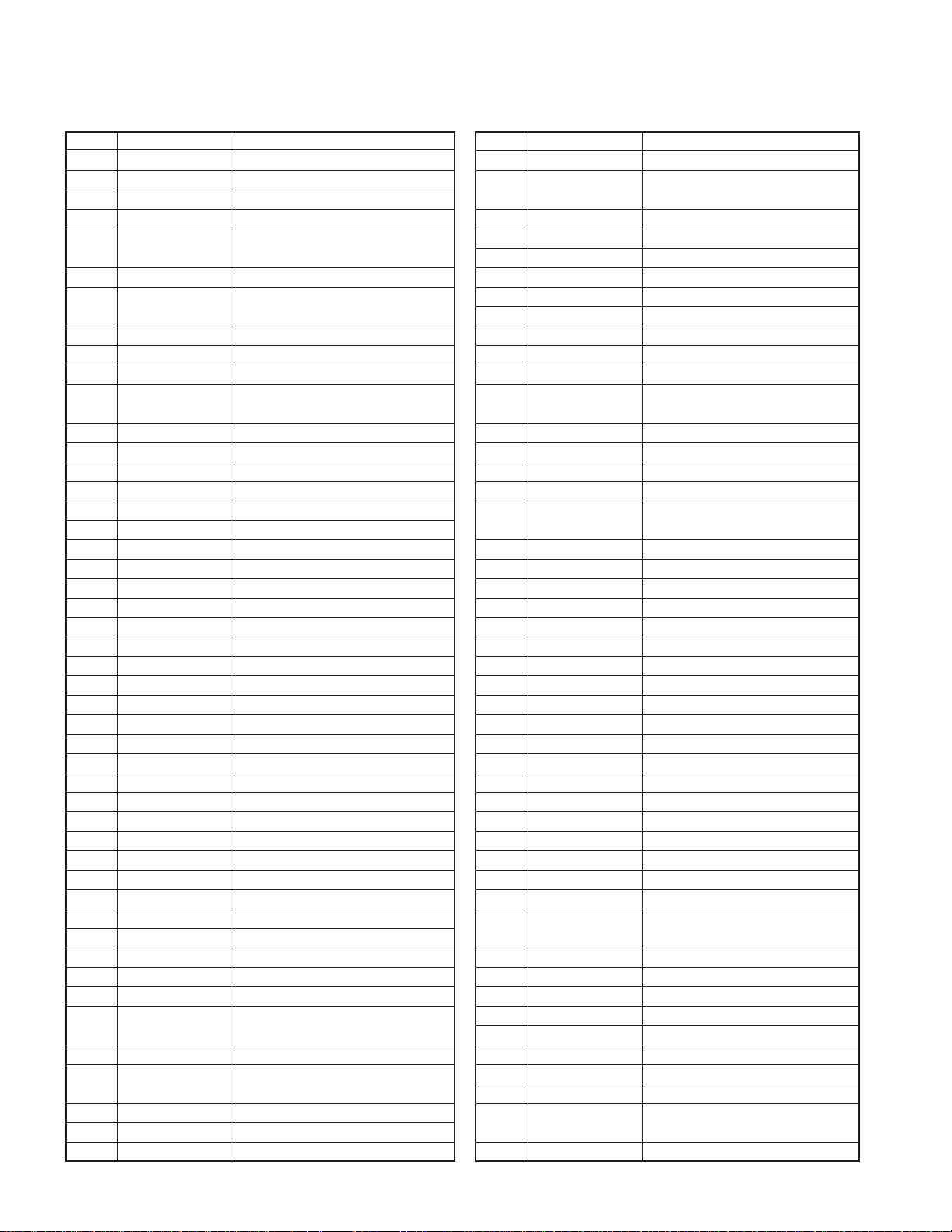
7-2. Transmission circuit
For the VHF VCO output, the 500MHz output passes through
the RF amplifier (Q13), is divided into 1/4 and amplified by
Q19. The signal passes through switch D101/D102, is amplified
by four amplifiers Q71, Q72, Q54, and Q56, and amplified to
the final output by power amplifier Q55. The signal passes
through a low-pass filter, an antenna switch, and another lowpass filter, and is sent to the antenna.
[(K only) The 220MHz VCO output is produced by passing
the 400MHz output through the RF amplifier (Q13), dividing it
into 1/2 by IC3, and amplifying it by Q19. The signal passes
through a switch (D101/D102), is amplified by four amplifiers
Q71/Q72/Q54/Q56, and amplified to the final output by power
amplifier Q57. The signal passes through a low-pass filter, an
antenna switch, and another low-pass filter, and is supplied
to the antenna.]
VCO
B
Q9MT6C03AE
D18 HVC131
D11,12
HVC3758
D21 HVC131
D10,16
HVC3758
AMP
Q13
2SC
5108(Y)
UHF
AMP
Q12
2SC
5009
AMP
5009
AMP
MT6C
03AE
SW
Q21
D99
2SC
HSC
277
Q93
D100
HSC
277
VOX
Q701
2SC4617
D709
VOXIN
Fig.19
DRIVE AMP DRIVE AMP
Q54
2SK
2973
TH-F6A/F7E
TONE & 96H AMP
3476
IC719
D53
D54
HVC131
VCO
Q9MT6C03AE
D18 HVC131
D11,12
HVC3758
D21 HVC131
D10,16
HVC3758
X1
TCX0
L77-1859-05
SW
D49 D85
D50 D86
D51
D52
HVC131
B
LPF
BPF
LPF
IC706
M62364
FP
AF AMP
IC720
HPF HPFSW
UHF
Q55
2SK
LPF
VHF
DTMF
PRE-EMPHASISMIC AMP
IC701
TA75W
558FU
The UHF VCO output is directly produced, passes through
RF amplifier Q13, and is amplified by Q93. It passes through
switch D100/D102, is amplified by four amplifiers Q71/Q72/
Q54/Q56, and amplified to the final output by power amplifier
Q55. It passes through a high-pass filter, an antenna switch,
and an antenna filter, and goes to the antenna.
RF POWER AMP
Q56
2SK
2973
ANT
DEVIDER
VHF
1509GV
UPB
AMP
IC3
5009
D101
Q19
HSC
2SC
277
7-3. APC circuit
The APC circuit is used to provide stable transmission
output, detects drain current of the power module and controls
transmission output. The voltage produced at R204, and R206
is amplified by IC8 and Q50, and the difference between the
voltage and the reference voltage of each band/power output
from the CPU (IC705) is detected by IC9 to produce APC
voltage. This voltage controls the gain of Q54, Q56, Q55, and
Q57.
Fig.20
7-4. Temperature protection circuit
To prevent thermal destruction of the final power amplifier,
the voltage of the thermistor TH1 installed near the power
module is monitored by the CPU IC705. If the prescribed
temperature is exceeded, the APC voltage is decreased to
reduce heat generation.
13
TH-F6A/F7E
DESCRIPTION OF COMPONENTS
● (X14-6750-00)
Ref. No.
IC1 Charge IC
IC2 PLL IC B band RX TX
IC3 PRESCALER divided into 1/2, 1/4, and 1/8
IC4
IC5 FM/AM IC 2nd mix, quadrature detection, AF
IC6 PLL IC for A band receiver
IC7 FM IC 2nd mix, quadrature detection, AF
IC8 APC Control Transmission APC control OP-AMP
IC9 APC Control Transmission APC control OP-AMP
IC10 Wide band AMP B band receiver 2nd amp
IC11 Shift register Shift register (ATT, power supply,
IC701 MIC&DTMF AMP Limiter amp, splatter filter
IC702 MIC AMP
IC703 AMP for packet
IC704 E2PROM
IC705 CPU for J, K, E type
IC706 Electronic VR
IC707 AF AMP
IC708 4.0 regulator
IC709 RESET IC
IC710 3.5V Detector
IC711 TONE FILTER CTCSS, ADCS
IC712
IC713
IC714 APC circuit Transmitter
IC715 3.0 regulator LCD booster Circuit
IC717 Rx AF AMP
IC718
IC719 TONE&96H AMP
IC720 AF AMP
D1 voltage shift Power supply voltage shift
D2
D4 Limiter
D5 Charge IC reverse current protector
D6
D7 voltage shift voltage shift
D8
D9 DC SW Speed up SW
D10-12
D16 VCO VCO
D18 VCO VCO shift SW
D20 Tuning
D21 VCO VCO shift SW
D24 Tuning
D25 RF SW FM/W-FM SW
D28 Tuning
D29 Tuning
DESCRIPTION NAME
Mixer for SSB detection
output, noise amp output, S-meter
output, noise amp output, S-meter
ANT SW, )
TONE DETECTOR
DC · DC converter
BPF Voltage adjus
reverse current protector
reverse current protector
PLL Lock voltage detect SW
VCO VCO
t B band RX TX
reverse current protector
reverse current protector
B band RX TX
SSB/CW 3rd LO oscillation frequency
tuning
SSB/CW 3rd LO oscillation frequency
tuning
A band local filter tuning
2rd LO oscillation frequency tuning
Use/function
Ref. No.
D32 ATT B band RF AGC ATT
D33
D34-37
D38 DC SW Speed up SW
D40 RF SW VCO shift SW
D41 RF SW A band VCO output SW
D44
D45 Limiter voltage limiter
D49 ANT SW
D51-54
D57 RF SW Bar antenna RF receve line SW
D58 POWER SW B band 2nd wide band amp power
D59 RF AMP SW
D60 Tuning Bar antenna frequency tuning
D62 ANT SW
D63
D65 RF SW B band RF receive line SW 600 to
D67 RF SW A band 265 to 680MHz
D68 RF SW B band 265 to 680MHz
D69
D70 ANT SW
D71 RF SW
D72 Tuning A band VHF BPF tuning
D73 ANT SW
D74 RF SW 220MHz band BPF tuning
D75-77
D78 RF SW B band 108 to 265MHz
D80 RF SW B band 50 to 108MHz
D81 Tuning A band VHF BPF tuning
D82 ANT SW
D83 Tuning A band VHF BPF tuning
D85 ANT SW
D87-90
D91 RF SW B band 0.1 to 50MHz
D93 ANT SW B band 50 to 105MHz
D94 ANT SW B band 0.1 to 50MHz
D95-97
D99 RF SW B band local 650 to 1.3GHz
D100 RF SW B band local 325 to 650MHz
D101 RF SW B band local 0.1 to 325MHz
D102 RF SW Transmission drive input SW
D103 SW Matching SW
D104 ANT SW
D106 Tuning A band local filter tuning
D107-110
D112,113
D114 ANT SW Transmission band SW
DESCRIPTION NAME
PLL Lock voltage detect SW
VCO VCO
reverse current protector
ANT SW
reverse current protector
UHF RF AMP SW
Tuning A band VHF BPF tuning
Tuning B band VHF BPF tuning
BPF tuning B band 50 to 108MHz receive BPF
RF SW B band PLL IC Fin filter SW
ANT SW Receiver circuit protector SW
A band PLL IC power supply voltage
shift
supply SW
1300MHz
UHF 1st amp control
A band VHF ( 220MHz K type only )
tuning
(ON:transmission)
Use/function
14
TH-F6A/F7E
DESCRIPTION OF COMPONENTS
Ref. No.
D115 RF SW
D116 ATT SW B band 50 to 108MHz ON:receive
D117,118
D119 ANT SW Q57 control SW
D120 ANT SW Q55 control SW
D121
D122 voltage shift
D123
D124,125
D126 voltage shift
D702-704
D705 AF rectification
D706-708 reverse current protector
D709 AF rectification
D710,711
D712-717
D718 AGC SW
D719
D720-725
D726
D727
D730-732 reverse current protector
Q1
Q2 Charge control
Q3 Charge control constant potential charge
Q4 SW B band/transmission PLL charge
Q5 Charge control
Q6 SW B band/transmission PLL VCO shift
Q7 RIPPLE FILTER B band/transmission VCO power
Q8 SW Prescaler divider SW
Q9 OSCILLATOR B band /transmission VCO
Q10
Q11 RF AMP
Q12 RF AMP
Q13 BUFFER AMP
Q14
Q15 SW Prescaler divider SW
Q17 SW Prescaler divider SW
Q19 RF SW B band local amp
Q21 RF AMP B band local amp
Q22 AF SW B band AF output SW
Q23 3rd local AMP 3rd local (crystal oscillator) buffer
Q24 IF AMP B band W-FM
Q25 AGC AMP B band IF AGC DC amp
Q26 BUFFER AMP B band IF AGC amp (57.6MHz)
Q27 local AMP B band 2nd local (crystal oscillator)
DESCRIPTION NAME
ATT on
ANT SW
reverse current protector
overvoltage protector
overinput protector
Type setting diode
overvoltage protector
LED
reverse current protector
LED
constant-voltage circuit
reverse current protector
constant-current circuit
VCO power supply SW
Power supply switch
constant current charge
pump SW
SW
supply
Prescaler power supply SW
amp
buffer amp
Use/function Ref. No.
DESCRIPTION NAME
Q28 MIXER B band
Q29 AF SW B band AF output SW
Q30 SW
Q31 RIPPLE FILTER A band VCO power supply
Q32 ANT SW Bar antenna switch
Q34 OSCILLATOR A band VCO oscillator
Q35
Q37 BUFFER AMP A band RX VCO output amp
Q40 RF AMP A band local amp
Q41 RF AMP A band mixer input amp
Q43 IF AMP A band 1st IF amp
Q44 RF AMP A band 2nd local multiplyng
Q45 MIXER A band
Q46 RF AMP B band 1.2GHz band 1st amp
Q47 APC SW APC control
Q48 ANT SW Bar antenna switch
Q49 APC controller APC control
Q50 AMP APC control
Q51 APC SW APC control
Q52 ANT SW Bar antenna switch
Q53 DC SW Bias control
Q54 RF AMP Pre-drive
Q55 RF AMP VHF/UHF final-amp
Q56 RF AMP Drive amp
Q57 RF AMP 220MHz band final-amp (K-type
Q58
Q59 RF AMP Bar antenna 1st amp
Q62 RF AMP UHF 1st amp (A/B band)
Q63 RF AMP A band VHF 1st amp
Q64 RF AMP B band VHF 1st amp
Q65
Q66 APC SW APC control
Q68 SW BPF SW
Q69 VCO switching VCO oscillator frequency shift SW
Q70 VCO switching VCO oscillator frequency shift SW
Q71 RF AMP Drive amp
Q72 RF AMP Pre-amp
Q73 BAND SW
Q74 BAND SW B band 50 or less On when RX
Q76 RF AMP
Q92
Q93 RF AMP B band local amp
Q94 RF SW PLL Fin filter SW
Q95,96
Q97 RF AMP B band local amp
Q98 GAIN SW Bar antenna RF amp gain SW
Q99 DC SW Bias control
Q100 IF SW when bar antenna use : ON
VCO power supply SW
Power supply switch
DC IN DETECT SW
Power supply switch
SW Final SW
B band FM / W-FM power supply SW
A band RX VCO power supply
switching
only)
B band 2nd amp power supply
control
DC-IN / battery
B band 50 to 108MHz On when RX
B band 50 to 108MHz On when RX
B band 1.2GHz band 1st amp
power supply SW
Use/function
15
TH-F6A/F7E
DESCRIPTION OF COMPONENTS / SEMICONDUCTOR DATA
Ref. No.
Q701 VOX AMP
Q702 impedance 9600bps transmitter
Q703 BEAT SHIFT
Q704 AF SP MUTE SW
Q705 RAMP SW
Q706 AF SP MUTE SW Ext speaker
Q707 MIC MUTE SW
Q708 AF SP MUTE SW
Q709 AUDIO AVR SW
Q710 AVR
Q712 VTx SW
Q713 VSSB&VRB SW
Q714 M4S SW
Q715 VRA&VCV SW
Q716 VVOX SW when VOX mode ON
Q719 Rx AF filter
Q720 RX packet AMP
Q721,722
Q723 TNC cotrol SW
Q725 Audio AVR
Q726 Voltage cotro SW
Q727 LCD DRIVE SW
Q728 AVR SW
Q729
DESCRIPTION NAME
impedance conversion
NOISE SHIFT SW
9600bps receiving
Use/function
● Microcomputer pin functions
:µPD784216(IC705)
Pin
I/O Pin name
No.
1 I LDB L B band PLL lock detect
2 I LDA L A band PLL lock detect
3 O PLF1 H PLL filter switch
4 I CHGI L charging detection
5 O VRBS L B band receiver power supply
6O
7O
8O
9 - --- --- Positive power supply
10 O --- --- System clock
11 I --- --- System clock
12 - --- --- Ground
13 - --- --- Open
14 - --- --- Connect to VSS
15 I RESET H System reset L:Reset[3.0V]
16 I INT Power supply voltage drop
17 O LEA A band PLL enable
18 O LEB --- B band PLL enable
19 I EN2 Encoder data input
20 I EN1 Encoder interrupt
21 I PWR L [PWR] Switch interrupt
22 I DCDET L DC-IN detection
23,24
25 I BATT --- Battery voltage level A/D input
26 I SQB --- B band noise level A/D input
27 I SMA --- A band S meter level A/D input
28 I SMB --- B band S meter level A/D input
29 I REM --- Remote control microphone
30 I VOXIn --- VOX sensitivity A/D input
31 I TOIn --- TONE detection input pin
32 I
33 - --- --- Connect to VSS
34 O
35 O TONE Subtone D/A output
36 - --- --- Connect to VDD
37 O SAVE L Save L:ON
BRXSW1
BRXSW2
BVCOSW
- --- --- Connect to VDD
SQA&THM
1750/DTMF
Active level
H:Lock
H:Lock
L:Charging
when receiving:L
H Prescaler
H Prescaler
H B band VCO double switch
H:Upper
detection interrupt 3.5[V]
H:Enable
H:Enable
L:pressed
L:DC-IN connect
key A/D input
---
A band noise level & temperature-
compensated thermistor voltage
A/D input
DTMF tone,1750Hz tone D/A
output
Function
16
SEMICONDUCTOR DATA
TH-F6A/F7E
Pin
I/O Pin name
No.
38 O LAPS H Key, LCD ilumination power
39 O AFC H Audio amp power supply SW,
40 I RxD1 L UART data input from PC pin
41 O TxD1 L UART data output to PC pin
42 O AFV L AF mute switch
43 O RESLCD H LCD driver resetL:Reset
44 O R0LCD --- LCD driver data type bit
45 O ELCD LCD driver enable
46 O RWLCD --- LCD driver read/write
47 O
48-55
56-60
61 I TYPE L Destination, channel display
62 O 96H H 9600BPSH:ON
63 O ABS TONE band switch
64-68
69 O LCK Shift register enable
70 I PTT2 L External [PTT] key input
71 O M4SS H M4SSW H:ON
72 - --- --- Ground
73 O BVCOS H B Band VCO select switch
74 O WFMS L W-FM switch L:WFM
75 O BAMS L B Band FM detector switch
76 O DACEN --- D/A enable
77 O SPM H Receiving on mute SW
78 O BMS H Band matching SW
79 O BUSY L 9600bps BUSY output
80 O BSHIFT L Beet shift SW H:ON
81 - --- --- Positive power supply
82 O VVOXS L VOX power supply
83 O VSSBS L SSB power supply
84 O
MIC MUTE
I/O D0-7 --- LCD driver data line
I KEYI1-5 L Key matrix input 1-5
O
KEYO1-5
APC/BPFA
Active level
supply H:ON
key,LCD ilumination, power
supply SW H:ON
L:DCS,CTCSS ON
L:Control H:Display
H:Enable
L:write
H Micmute switch H:MUTE
mode diode input
H:B band L:A band
L Key matrix output 1-5
H:ON
L:pressed
H:VCO2
L:FM,WFM mode
L:MUTE
H:BUSY
VOX ON, at TX:L
L:SSB,CW
--- APC & A BPF tuning PWM
output 144,220MHz band
recive
Function
Pin
I/O Pin name
No.
85 O BPFB --- B band BPF PWM output
86 O VRAS L A Band receiver power supply
87 O BEEP Beep output
88 I SI EEPROM data input line
89 O CLK Common clock line
90 O DATA Common data line
91 O CS EEPROM chip select
92 O VTXS L Transmission power supply
93 O VCVS L
94 I
95 O RLEDA L A band busy LED L:ON
96 O TLEDA L A band transmission LED
97 O RLEDB L B band busy LED L:ON
98 O TLEDB L B band transmission LED
99 I PTT1 L PTT SW(main)
100 O TXL H Transmission VCO1 shift
VPP/TEST
Active level
Function
input with the bar antenna
Receiving:L
(EEPROM SO pin)
L:Enable
L:Transmission
B band VCO, PLL power supply
switch
Flash write 10V application pin
Normally:L
L:ON
L:ON
L:Transmisson
H:Shift ON
L:B band ON
17
TH-F6A/F7E
● Terminal Functions
Connecter No.NOName Terminal function
CN7 1
CN716 4 CHGI Charge detect interrupt
CN8 1 GND GND
18
APC & TUNEA
2 BMS Band matching switch
3 PLF1 PLL filter switch
5 LDB B band PLL lock detection
6 BVCOSW B band VCO doubler SW
7 DCDET DC-IN detection
8 LDA A band PLL lock detection
9 SW1 Prescaler divide
10 SW2 Prescaler divide
11 LEB B band PLL enable
12 AFB B band audio output
13 LEA A band PLL enable
14 AFA A band audio output
15 FINE2 3rd local control voltage
16 B Battery power
17 FINE1 2nd local control voltage
18 MOD Modulation signal input
19 LCK Shift register enable
20 CLK Common clock
21 TXL VCO shift
22 DATA Common data
THM&SQA
23
24 C8 Charge pump power supply
25 SMB B band S-meter voltage
26 VTX Transmission power supply
27 SQB B band squelch voltage
28 VRB B band RX voltage
29 SMA A band s meter voltage
30 VRA A band RX power supply
31 M4S AVR power supply
32 VCV B band VCO, PLL power supply
33 VTUNEB B band BPF tuning voltage
34 VC Power supply
35 BAMS B band AM power supply
36 BSS B band PLL fin filter switch
37 VXTAL TCXO modulation signal
38 WFMS W-FM power supply
39 GND GND
40 VSSB SSB,CW power supply
2 MBCV B band VCO control voltage
3 MACV A band VCO control voltage
4 MOD Modulation signal
5 MAVCOS A band VCO SW
6 BSS B band PLL fin filter SW
7 A220S A band PLL fin filter SW
8 TXL B band VCO shift
9 VRA A band RX power supply
10 VCV B band VCO, PLL power supply
11 MAOUT A band VCO output signal
APC&A band BPF tuning voltage
Thermal detection & A band
squelch voltage
SEMICONDUCTOR DATA
Connecter No.NOName Terminal function
CN8 12 MBOUT B band VCO output signal
CN9 1 GND GND
2 DBCV B band VCO control voltage
3 DACV A band VCO control voltage
4 DMOD Modulation signal
5 DAVCOS A band VCO SW
6 DBSS B band VCO SW
7 DA220S A band VCO shift
8 DTXL B band VCO shift
9 DVRA A band RX power supply
10 DVCV B band VCO, PLL power supply
11 DAOUT A band VCO output signal
12 DBOUT B band VCO, output signal
CN713 1 NC NC
2 IM1 Interface mode specify
OPDFF/TES
3
/IMO/ID
4-11 DB7-0 LCD driver data bus
12 RESET LCD driver data reset
13 CS Chip select signal (L)
14 RS
15 E LCD driver enable
16 RW/RD LCD driver read /write
17 GND GND
18 OSC2 CR oscillator
19 OSC1 CR oscillator
20 Vcc Power supply
21 Vci Reference voltage output,
22 C1+ Boost voltage circuit
23 C1- Boost voltage circuit
24 VLOUT Boost voltage output
25 VLCD LCD power supply
26 V1OUT output voltage V1
27 V2OUT output voltage V2
28 V3OUT output voltage V3
29 V4OUT output voltage V4
30 V5OUT output voltage V5
CN714 1 GND GND
2 AFVO AF output
3 AFVI AF input
4 EN2 Encoder pulse 2
5 GND GND
6 EN1 Encoder pulse 1
CN715 1 SP+ SP
2 SP- GND
Parallel ·bus specify
LCD driver register select signal
boost circuit power supply
PARTS LIST
∗
New Parts. indicates safety critical components.
Parts without Parts No. are not supplied.
Les articles non mentionnes dans le Parts No. ne sont pas fournis.
Teile ohne Parts No. werden nicht geliefert.
TH-F6A/F7E
TX-RX UNIT (X57-6360-00)
Ref. No.
11A∗ A02-3727-03 CABINET ASSY
23A∗ A10-4050-01 CHASSIS
33B∗ A82-0046-02 REAR PANEL
41B∗ B09-0615-23 CAP (MIC/SP/DC)
51A∗ B10-2685-13 FRONT GLASS T,E
51A∗ B10-2723-13 FRONT GLASS K
62B∗ B11-1280-04 ILLUMINATION GUIDE (LCD)
72B∗ B11-1281-04 FILTER (LCD)
82B∗ B38-0852-15 LCD ASSY
9-∗ B62-1441-00 INSTRUCTION MANUAL(ENG/SPA)
9-∗ B62-1442-00 INSTRUCTION MANUAL(FRE/ITA) E
9-∗ B62-1443-00 INSTRUCTION MANUAL(NET/GER) E
10 - ∗ B72-2054-14 MODEL NAME PLATE K
10 - ∗ B72-2055-04 MODEL NAME PLATE T,E
11 2B ∗ D21-0856-04 SHAFT (RELEASE)
12 3B E04-0407-15 RF COAXIAL RECEPTACLE(SMA)
13 2B ∗ E23-1177-04 RELAY TERMINAL (BATTERY)
14 2B ∗ E23-1180-04 GROUND TERMINAL(SMA)
15 1B E37-0695-05 LEAD WIRE WITH CONNECTOR(SP)
16 - ∗ F07-1859-03 COVER (HOOK)
17 2B ∗ F10-2411-04 SHIELDING COVER(ANTENNA)
18 2A ∗ F10-2437-04 SHIELDING PLATE(BAR-ANTENNA)
19 1B ∗ F12-0464-14 SHIELDIBG SHEET(LCD)
20 1B ∗ F15-1002-04 SHADOW PLATE (LCD)
21 1B ∗ F15-1004-04 SHADOW PLATE (TX-RX)
23 2A ∗ F20-3325-04 INSULATING SHEET
24 1B,2B ∗ F20-3336-04 INSULATING SHEET
25 2B ∗ G01-4532-04 COIL SPRING (RELEASE)
26 3A ∗ G11-4060-04 RUBBER SHEET
27 3A ∗ G13-1858-14 CUSHION (CHASSIS)
28 2A ∗ G13-1860-04 CUSHION (BAR-ANTENNA)
29 3B ∗ G53-1529-04 PACKING (VOL/ENC)
30 3A ∗ G53-1532-02 PACKING (CASE)
31 2A ∗ G53-1533-03 PACKING (MOLTI-F)
32 2B ∗ G53-1534-13 PACKING (SP/MIC)
33 - ∗ H52-1857-02 ITEM CARTON CASE K
33 - ∗ H52-1858-02 ITEM CARTON CASE T,E
34 3A ∗ J19-5428-03 HOLDER (TERMINAL)
35 2A ∗ J19-5429-13 HOLDER (BER-ANTENNA)
36 2B ∗ J21-8419-03 HARDWARE FIXTURE(LCD)
37 - J29-0623-04 BELT HOOK
38 2A ∗ J32-0927-04 CYLINDRICAL BOSS
39 - J69-0342-05 HANDSTRAP
40 2B ∗ J82-0076-05 FPC (VOL/ENC)
41 1B ∗ K29-5150-03 KNOB (VOL)
42 1B ∗ K29-5159-03 KNOB (ENC)
43 2A ∗ K29-9107-12 KEY TOP
44 1A ∗ K29-9108-13 KNOB (PTT/MONI)
!
Adrress
New
Parts No. Description
parts
TH-F6A/F7E
TH-F6A/F7E
L:
Scandinavia
Y:
PX (Far East, Hawaii)
Y:
AAFES (Europe)
Destination Destination
Ref. No.
45 2B ∗ K29-9109-03 LEVER KNOB (RELEASE)
46 1A ∗ K29-9110-03 KNOB (PTT)
47 1A ∗ K29-9111-03 KNOB (MULTI-F)
48 - L79-1417-05 LINE FILTER T,E
A 3B N09-1492-05 PAN HEAD SCREW (SMA)
B-∗ N09-2385-05 BINDING HEAD SCREW (HOOK)
C 1B N14-0573-04 CIRCULAR NUT (SMA)
D1B∗ N14-0593-04 CIRCULAR NUT (VOL/ENC)
E 2A N79-2035-45 PAN HEAD TAPTITE SCREW
F 2A,2B ∗ N79-2040-46 PAN HEAD TAPTITE SCREW
G 3A N80-2008-45 PAN HEAD TAPTITE SCREW
H 2A N83-2006-45 PAN HEAD TAPTITE SCREW
49 2B R39-0602-05 VARIABLE RESISTOR
SP 1B T07-0266-05 SPEAKER
50 - ∗ T90-0781-05 WHIP ANTENNA K
50 - ∗ T90-0789-05 WHIP ANTENNA T,E
ANT 2A ∗ T90-0787-05 ANTENNA (Bar antenna)
51 - ∗ W08-0927-05 AC ADAPTER K
51 - ∗ W08-0928-05 AC ADAPTER E
51 - ∗ W08-0929-05 AC ADAPTER T
53 3A X57-6362-01 VCO UNIT
Adrress
TX-RX UNIT (X57-6360-00) 0-11:K, 2-71:T,E
D712,713 B30-2131-05 LED
D714-717 B30-2210-05 LED(TLY)
D720-725 B30-2157-05 LED(YELLOW)
C1 CK73HB1H471K CHIP C 470PF K
C2 CK73HB1H102K CHIP C 1000PF K
C3,4 CC73HCH1H101J CHIP C 100PF J
C5 CK73HB1H102K CHIP C 1000PF K
C6 CK73HB1C103K CHIP C 0.010UF K
C7 CK73HB1A104K CHIP C 0.10UF K
C8 CK73HB1H471K CHIP C 470PF K
C9,10 CK73HB1C103K CHIP C 0.010UF K
C11 CK73HB1H471K CHIP C 470PF K
C12 CC73HCH1H680J CHIP C 68PF J
C13 CK73HB1A104K CHIP C 0.10UF K
C14 CC73HCH1H120J CHIP C 12PF J
C15,16 CK73HB1A104K CHIP C 0.10UF K
C17,18 CK73HB1H471K CHIP C 470PF K
C19 CK73GB0J105K CHIP C 1.0UF K
C20 CK73HB1C103K CHIP C 0.010UF K
C21 CC73HCH1H102J CHIP C 1000PF J
C22 CK73HB1H471K CHIP C 470PF K
C23 CK73HB1H102K CHIP C 1000PF K
C24 CC73HCH1H101J CHIP C 100PF J
C25 CC73HCH1H680J CHIP C 68PF J
C26-28 CC73HCH1H220J CHIP C 22PF J
C29,30 CK73HB1A104K CHIP C 0.10UF K
C31,32 CK73HB1H471K CHIP C 470PF K
C33 CK73HB1H102K CHIP C 1000PF K
K:
New
parts
USA
T:
England
X:
Australia
P:
Canada
E:
Europe
M:
Other Areas
Parts No. Description
19

TH-F6A/F7E
TX-RX UNIT (X57-6360-00)
New
Ref. No.
C34 CC73HCH1H101J CHIP C 100PF J
C36 C92-0518-05 CHIP-TAN 0.22UF 20WV
C37 CK73HB1H471K CHIP C 470PF K
C40 CK73HB1C103K CHIP C 0.010UF K
C41 C92-0766-05 CHIP-TAN 4.7UF 6.3WV
Adrress
Parts No. Description
parts
PARTS LIST
New
Destination Destination
Ref. No.
C123 CC73HCH1H101J CHIP C 100PF J
C126 CK73FB1C105K CHIP C 1.0UF K
C127 CK73HB1C103K CHIP C 0.010UF K
C129 CK73HB1C103K CHIP C 0.010UF K
C130 CK73HB1H332K CHIP C 3300PF K
Adrress
Parts No. Description
parts
C42 CK73HB1C103K CHIP C 0.010UF K
C43 C92-0555-05 CHIP-TAN 0.047UF 35WV
C44 CK73HB1H471K CHIP C 470PF K
C45 C92-0542-05 CHIP-TAN 0.10UF 20WV
C46 CK73HB1C103K CHIP C 0.010UF K
C47,48 CK73HB1H471K CHIP C 470PF K
C49 CC73HCH1H0R5B CHIP C 0.5PF B
C50 CC73HCH1H010B CHIP C 1.0PF B
C51 CK73HB1H471K CHIP C 470PF K
C52 C92-0772-05 CHIP-TAN 10UF 6.3WV
C53 CK73HB1H471K CHIP C 470PF K
C54 CK73HB1A104K CHIP C 0.10UF K
C55-57 CK73HB1H471K CHIP C 470PF K
C58,59 CK73HB1A104K CHIP C 0.10UF K
C60-62 CK73HB1H471K CHIP C 470PF K
C64 CK73HB1C103K CHIP C 0.010UF K
C65 CC73HCH1H060B CHIP C 6.0PF B
C66 CC73HCH1H150J CHIP C 15PF J
C67 CC73HCH1H060B CHIP C 6.0PF B
C68,69 CK73HB1H471K CHIP C 470PF K
C70 CK73HB1C103K CHIP C 0.010UF K
C71 CC73HCH1H070B CHIP C 7.0PF B
C72 CK73HB1H471K CHIP C 470PF K
C75 ∗ CC73HCH1H100C CHIP C 10PF C
C76,77 CK73HB1H471K CHIP C 470PF K
C78 CC73HCH1H0R5B CHIP C 0.5PF B
C79,80 CK73HB1H471K CHIP C 470PF K
C82 CC73HCH1H0R5B CHIP C 0.5PF B
C83 CC73HCH1H220J CHIP C 22PF J
C84,85 CK73HB1C103K CHIP C 0.010UF K
C133,134 CK73HB1C103K CHIP C 0.010UF K
C135 CK73HB1A104K CHIP C 0.10UF K
C137 CK73HB1H152K CHIP C 1500PF K
C138 CK73HB1A104K CHIP C 0.10UF K
C139 CC73HCH1H101J CHIP C 100PF J
C140 CK73HB1H821K CHIP C 820PF K
C141 CK73HB1C103K CHIP C 0.010UF K
C143 CK73HB1C103K CHIP C 0.010UF K
C145 CK73HB1H102K CHIP C 1000PF K
C147 C92-0772-05 CHIP-TAN 10UF 6.3WV
C149 CK73GB1A474K CHIP C 0.47UF K
C150 CK73HB1A104K CHIP C 0.10UF K
C151 CK73HB1H102K CHIP C 1000PF K
C152 CK73HB1A104K CHIP C 0.10UF K
C154 CK73HB1H102K CHIP C 1000PF K
C155 C92-0772-05 CHIP-TAN 10UF 6.3WV
C156,157 CK73HB1H102K CHIP C 1000PF K
C158-160 CK73HB1A104K CHIP C 0.10UF K
C161 CK73HB1H102K CHIP C 1000PF K
C162 CK73HB1A104K CHIP C 0.10UF K
C163,164 CC73HCH1H101J CHIP C 100PF J
C165 CK73HB1A104K CHIP C 0.10UF K
C166 CC73HCH1H330J CHIP C 33PF J
C167 CC73HCH1H070B CHIP C 7.0PF B
C168 CK73HB1A104K CHIP C 0.10UF K
C169 C92-0772-05 CHIP-TAN 10UF 6.3WV
C170-173 CK73HB1A104K CHIP C 0.10UF K
C174 CK73HB1H102K CHIP C 1000PF K
C175 CK73HB1A104K CHIP C 0.10UF K
C177 C92-0772-05 CHIP ELECTR 470UF 10WV
C86,87 CK73HB1H471K CHIP C 470PF K
C88 CK73HB1A104K CHIP C 0.10UF K
C89 CK73HB1H471K CHIP C 470PF K
C90,91 ∗ CC73HCH1H100C CHIP C 10PF C
C94 CC73HCH1H080B CHIP C 8.0PF B
C95 CC73HCH1H030C CHIP C 3.0PF C
C97 CC73HCH1H080B CHIP C 8.0PF B
C102,103 CK73HB1C103K CHIP C 0.010UF K
C104 CK73HB1H471K CHIP C 470PF K
C105 CK73HB1H102K CHIP C 1000PF K
C106 CK73HB1H471K CHIP C 470PF K
C107 CC73HCH1H050C CHIP C 5.0PF C
C108 ∗ CC73HCH1H100C CHIP C 10PF C
C109,110 CK73HB1H471K CHIP C 470PF K
C112 CK73HB1H102K CHIP C 1000PF K
C113 CK73HB1H471K CHIP C 470PF K
C114,115 CC73HCH1H101J CHIP C 100PF J
C116 CC73HCH1H050C CHIP C 5.0PF C
C117 CC73HCH1H101J CHIP C 100PF J
C119 CK73HB1C103K CHIP C 0.010UF K
C121 CC73HCH1H060B CHIP C 6.0PF B
20
C178 CK73HB1H102K CHIP C 1000PF K
C179 CK73HB1A104K CHIP C 0.10UF K
C180 CC73HCH1H030C CHIP C 3.0PF C
C181 CK73HB1C103K CHIP C 0.010UF K
C182 CC73HCH1H120J CHIP C 12PF J
C183,184 CK73HB1C103K CHIP C 0.010UF K
C186 CC73HCH1H270J CHIP C 27PF J
C188 CC73HCH1H050C CHIP C 5.0PF C
C189 ∗ CC73HCH1H100C CHIP C 10PF C
C190 CC73HCH1H120J CHIP C 12PF C
C191 CK73HB1A104K CHIP C 0.10UF K
C192 CK73HB1C103K CHIP C 0.010UF K
C193 CC73HCH1H060B CHIP C 6.0PF B
C195 CK73HB1H471K CHIP C 470PF K
C196 CC73HCH1H220J CHIP C 22PF J
C199 CC73HCH1H121J CHIP C 120PF J
C200 CK73HB1H102K CHIP C 1000PF K
C202 CK73HB1C103K CHIP C 0.010UF K
C203 CC73HCH1H330J CHIP C 33PF J
C205,206 CK73HB1C103K CHIP C 0.010UF K
C208 CK73HB1C103K CHIP C 0.010UF K

New
Ref. No.
C209 CC73HCH1H101J CHIP C 100PF J
C210 CC73HCH1H330J CHIP C 33PF J
C211 CK73HB1C103K CHIP C 0.010UF K
C212,213 CC73HCH1H101J CHIP C 100PF J
C214 CK73HB1H102K CHIP C 1000PF K
Adrress
Parts No. Description
parts
TH-F6A/F7E
PARTS LIST
TX-RX UNIT (X57-6360-00)
New
Destination Destination
Ref. No.
C283 CK73HB1H471K CHIP C 470PF K
C284 CC73HCH1H090D CHIP C 9.0PF D
C285 CC73HCH1H820J CHIP C 82PF J
C286 CK73HB1A104K CHIP C 0.10UF K
C287 CK73HB1A104K CHIP C 0.10UF K
Adrress
Parts No. Description
parts
C215 CK73HB1C103K CHIP C 0.010UF K
C217 ∗ CC73HCH1H100C CHIP C 10PF C
C218 CC73HCH1H470J CHIP C 47PF J
C219 CK73HB1H471K CHIP C 470PF K
C220,221 CK73HB1A104K CHIP C 0.10UF K
C222 CK73HB1H471K CHIP C 470PF K
C223 CK73HB1H102K CHIP C 1000PF K
C224 CC73HCH1H470J CHIP C 47PF J
C225,226 CK73HB1H471K CHIP C 470PF K
C227 CK73HB1H561K CHIP C 560PF K
C228 C92-0003-05 CHIP-TAN 0.47UF 25WV
C229 C92-0766-05 CHIP-TAN 4.7UF 6.3WV
C230 C92-0555-05 CHIP-TAN 0.047UF 35WV
C231,232 CK73HB1H471K CHIP C 470PF K
C233 CK73HB1A104K CHIP C 0.10UF K
C234 CK73HB1H561K CHIP C 560PF K
C235 C92-0772-05 CHIP-TAN 10UF 6.3WV
C236 CK73HB1H471K CHIP C 470PF K
C237 CK73HB1A104K CHIP C 0.10UF K
C238 CK73HB1C103K CHIP C 0.010UF K
C239 CK73HB1H561K CHIP C 560PF K
C240,241 CC73HCH1H010B CHIP C 1.0PF B
C242 CC73HCH1E181J CHIP C 180PF J
C245 CK73HB1H102K CHIP C 1000PF K
C246 CC73HCH1H070B CHIP C 7.0PF B
C247 ∗ CC73HCH1H100C CHIP C 10PF C
C248 CC73HCH1H120J CHIP C 12PF J
C249 CK73HB1H471K CHIP C 470PF K
C251 CK73HB1H471K CHIP C 470PF K
C252 CC73HCH1H070B CHIP C 7.0PF B
C288 CK73HB1A104K CHIP C 0.10UF K
C289 CC73HCH1H330J CHIP C 33PF J
C290,291 CC73HCH1E181J CHIP C 180PF J
C292 CK73HB1A104K CHIP C 0.10UF K
C293 CK73HB1H102K CHIP C 1000PF K
C295 CK73HB1C103K CHIP C 0.010UF K
C296 CC73HCH1H150J CHIP C 15PF J
C297 CC73HCH1H560J CHIP C 56PF J
C298,299 CK73HB1H102K CHIP C 1000PF K
C301 C92-0772-05 CHIP-TAN 10UF 6.3WV
C302 CK73HB1H471K CHIP C 470PF K
C303 CC73HCH1H080B CHIP C 8.0PF B
C305 CK73HB1H102K CHIP C 1000PF K
C306 CC73HCH1H150J CHIP C 15PF J
C307 CK73HB1C103K CHIP C 0.010UF K
C308 CK73HB1H471K CHIP C 470PF K
C309 CK73HB1C103K CHIP C 0.010UF K
C310-314 CK73HB1H471K CHIP C 470PF K
C315 CC73HCH1H220J CHIP C 22PF J
C317-322 CK73HB1H471K CHIP C 470PF K
C323 C92-0772-05 CHIP-TAN 10UF 6.3WV
C324-328 CK73HB1H471K CHIP C 470PF K
C331,332 CK73HB1H471K CHIP C 470PF K
C333 CC73HCH1H330J CHIP C 33PF J
C334,335 CK73HB1H471K CHIP C 470PF K
C336 CK73HB1H102K CHIP C 1000PF K
C337 CC73HCH1H470J CHIP C 47PF J
C338 CC73HCH1H270J CHIP C 27PF J
C339 CK73GB1H471K CHIP C 470PF K
C340 CK73HB1A104K CHIP C 0.10UF K
C253 CK73HB1H561K CHIP C 560PF K
C254 CC73HCH1H0R5B CHIP C 0.5PF B
C255 CK73HB1H471K CHIP C 470PF K
C256 CK73HB1C103K CHIP C 0.010UF K
C259 CC73HCH1H0R5B CHIP C 0.5PF B
C260 ∗ CC73HCH1H100C CHIP C 10PF C
C261 CK73HB1H471K CHIP C 470PF K
C263 ∗ CC73HCH1H100C CHIP C 10PF C
C264 CC73HCH1H220J CHIP C 22PF J
C265 CK73HB1H471K CHIP C 470PF K
C266 CK73HB1A104K CHIP C 0.10UF K
C269 CC73HCH1H120J CHIP C 12PF J
C270 CC73HCH1H020B CHIP C 2.0PF B
C271 CC73HCH1H120J CHIP C 12PF J
C272 ∗ CC73HCH1H100C CHIP C 10PF C
C274 CC73HCH1H101J CHIP C 100PF J
C277 CK73HB1H561K CHIP C 560PF K
C278 CC73HCH1H0R5B CHIP C 0.5PF B
C280 CK73FB1C105K CHIP C 1.0UF K
C281 CK73HB1C103K CHIP C 0.010UF K
C282 CC73HCH1H150J CHIP C 15PF J
C341 CC73HCH1H070B CHIP C 7.0PF B
C343 CC73HCH1H120J CHIP C 12PF J
C344 CC73HCH1H150J CHIP C 15PF J
C345-347 CK73HB1H471K CHIP C 470PF K
C348,349 CC73GCH1H680J CHIP C 68PF J
C350 CC73GCH1H270J CHIP C 27PF J
C351 CC73GCH1H220J CHIP C 22PF J K
C351 CC73GCH1H270J CHIP C 27PF J T,E
C352 CK73HB1H471K CHIP C 470PF K
C353 CK73FB1C105K CHIP C 1.0UF K
C354 CC73GCH1H330J CHIP C 33PF J K
C354 CC73GCH1H360J CHIP C 36PF J T,E
C356 CC73GCH1H270J CHIP C 27PF J K
C356 CC73GCH1H330J CHIP C 33PF J T,E
C357 CC73GCH1H120J CHIP C 12PF J
C358 CC73HCH1H101J CHIP C 100PF J
C360,361 CK73HB1H471K CHIP C 470PF K
C362 CK73HB1C103K CHIP C 0.010UF K
C363 CC73GCH1H130J CHIP C 13PF J
C368 CK73HB1H471K CHIP C 470PF K
C373 CC73GCH1H220J CHIP C 22PF J
21
TH-F6A/F7E
TX-RX UNIT (X57-6360-00)
New
Ref. No.
C376 CC73HCH1H050C CHIP C 5.0PF C K
C377 CK73HB1A104K CHIP C 0.10UF K
C378 CK73HB1H471K CHIP C 470PF K
C381 CC73HCH1H101J CHIP C 100PF J
C382 CC73GCH1H200J CHIP C 20PF J K
Adrress
Parts No. Description
parts
PARTS LIST
New
Destination Destination
Ref. No.
C463-474 CK73HB1C103K CHIP C 0.010UF K
C475 CK73HB1H471K CHIP C 470PF K
C476,477 CK73HB1C103K CHIP C 0.010UF K
C484 CC73GCH1H020B CHIP C 2.0PF B K
C484 CC73GCH1H030C CHIP C 3.0PF C T,E
Adrress
Parts No. Description
parts
C387,388 CK73HB1H102K CHIP C 1000PF K
C389 CC73HCH1H080B CHIP C 8.0PF B
C390 CK73HB1A104K CHIP C 0.10UF K
C392 CC73HCH1H150J CHIP C 15PF B K
C395 CK73HB1H102K CHIP C 1000PF K
C396 CK73HB1H471K CHIP C 470PF K
C407 CC73GCH1H100C CHIP C 10PF C
C408 CC73HCH1H050C CHIP C 5.0PF C K
C408 CC73HCH1H070B CHIP C 7.0PF B T,E
C409 CC73GCH1H150J CHIP C 15PF J K
C409 CC73GCH1H220J CHIP C 22PF J T,E
C410 CC73GCH1H010B CHIP C 1.0PF B K
C410 CC73GCH1H020B CHIP C 2.0PF B T,E
C411 CK73HB1H471K CHIP C 470PF K
C412 CC73HCH1H020B CHIP C 2.0PF B
C413 CC73HCH1H050C CHIP C 5.0PF C
C414 CC73GCH1H080D CHIP C 8.0PF D
C415 CC73HCH1H010B CHIP C 1.0PF B
C416 CC73GCH1H110J CHIP C 11PF J
C417 CC73HCH1H0R5B CHIP C 0.5PF B
C418 CC73GCH1H040B CHIP C 4.0PF B
C419 CC73GCH1H220J CHIP C 22PF J
C420 CC73HCH1H101J CHIP C 100PF J
C421 ∗ CC73HCH1H100C CHIP C 10PF C
C428 CC73HCH1H050C CHIP C 5.0PF C K
C428 CC73HCH1H070B CHIP C 7.0PF B T,E
C429 CC73GCH1H180J CHIP C 18PF J
C430 CC73GCH1H070B CHIP C 7.0PF B
C436 CC73HCH1H090D CHIP C 9.0PF D
C437 CC73HCH1H220J CHIP C 22PF J
C438 CC73HCH1H050C CHIP C 5.0PF C
C439 CC73HCH1H040C CHIP C 4.0PF C
C440 CC73HCH1H060B CHIP C 6.0PF B
C441 CC73HCH1H120J CHIP C 12PF J
C442 CK73HB1A104K CHIP C 0.10UF K
C443 CK73HB1H471K CHIP C 470PF K
C444 CK73HB1C103K CHIP C 0.010UF K
C445 CC73HCH1H101J CHIP C 100PF J
C446 CK73HB1A104K CHIP C 0.10UF K
C447 ∗ CC73HCH1H1R5B CHIP C 1.5PF B
C448 CK73HB1C103K CHIP C 0.010UF K
C449 CK73HB1H471K CHIP C 470PF K
C450 CK73HB1C103K CHIP C 0.010UF K
C451 CK73HB1A104K CHIP C 0.10UF K
C453 CK73HB1C103K CHIP C 0.010UF K
C454,455 CK73HB1A104K CHIP C 0.10UF K
C457 CK73HB1C223K CHIP C 0.022UF K
C458 CK73HB1A104K CHIP C 0.10UF K
C460 CK73HB1H471K CHIP C 470PF K
C461,462 CK73HB1A104K CHIP C 0.10UF K
C485 CC73HCH1H470J CHIP C 47PF J
C488 CC73HCH1H030C CHIP C 3.0PF C
C489 CC73HCH1H101J CHIP C 100PF J
C490 CC73HCH1H470J CHIP C 47PF J
C491 CC73HCH1H101J CHIP C 100PF J
C492 CC73HCH1H101J CHIP C 100PF J
C494 CK73HB1H471K CHIP C 470PF K
C495 CC73HCH1H150J CHIP C 15PF J T,E
C497 CC73HCH1H040C CHIP C 4.0PF C
C498 CC73HCH1H030C CHIP C 3.0PF C T,E
C498 CC73HCH1H150J CHIP C 15PF J K
C499 CC73HCH1H050B CHIP C 5.0PF C K
C499 ∗ CC73HCH1H130J CHIP C 13PF J T,E
C500 CC73HCH1H080B CHIP C 8.0PF B K
C500 CC73HCH1H040C CHIP C 4.0PF C T,E
C501 CC73HCH1H040C CHIP C 4.0PF C
C502 CC73HCH1H050C CHIP C 5.0PF C K
C502 CC73HCH1H150J CHIP C 15PF J T,E
C503 CC73HCH1H101J CHIP C 100PF J
C504 CC73HCH1H070B CHIP C 7.0PF B T,E
C504 CC73HCH1H120J CHIP C 12PF J K
C505 CK73HB1H471K CHIP C 470PF K
C506 CC73HCH1H060B CHIP C 6.0PF B K
C506 CC73HCH1H180J CHIP C 18PF J T,E
C507 CC73HCH1H080B CHIP C 8.0PF B K
C507 CC73HCH1H220J CHIP C 22PF J T,E
C508-510 CK73HB1H471K CHIP C 470PF K
C511 CC73HCH1H050C CHIP C 5.0PF C K
C511 ∗ CC73HCH1H100C CHIP C 10PF C T,E
C512,513 CK73HB1H102K CHIP C 1000PF K
C515,516 CK73HB1H102K CHIP C 1000PF K
C517 CC73HCH1H0R5B CHIP C 0.5PF B
C518 CC73HCH1H010B CHIP C 1.0PF B
C519-522 CK73HB1H102K CHIP C 1000PF K
C523 CC73GCH1H101J CHIP C 100PF J
C524 CK73HB1H561K CHIP C 560PF K
C525 CK73HB1H102K CHIP C 1000PF K
C527 CC73HCH1H030C CHIP C 3.0PF C
C528 CK73HB1H102K CHIP C 1000PF K
C529 CC73HCH1H101J CHIP C 100PF J
C531 CC73HCH1H101J CHIP C 100PF J
C532 CC73HCH1H560J CHIP C 56PF J
C533 CC73HCH1H330J CHIP C 33PF J
C534 CC73HCH1H220J CHIP C 22PF J
C535 CC73HCH1H330J CHIP C 33PF J
C536 CK73HB1H102K CHIP C 1000PF K
C537 CC73HCH1H560J CHIP C 56PF J
C538 CK73HB1H102K CHIP C 1000PF K
C539 CC73HCH1H470J CHIP C 47PF J
C543 CK73HB1H102K CHIP C 1000PF K
C544,545 CC73HCH1H680J CHIP C 68PF J
22
New
Ref. No.
C546-548 CK73HB1E472K CHIP C 4700PF K
C549 CK73HB1H102K CHIP C 1000PF K
C551 CC73HCH1H560J CHIP C 56PF J
C552 CC73HCH1H121J CHIP C 120PF J
C553 CC73HCH1H560J CHIP C 56PF J
Adrress
Parts No. Description
parts
TH-F6A/F7E
PARTS LIST
TX-RX UNIT (X57-6360-00)
New
Destination Destination
Ref. No.
C654 CC73GCH1H150J CHIP C 15PF J
C655 CK73HB1H471K CHIP C 470PF K
C656,657 CK73HB1A104K CHIP C 0.10UF K
C658 CC73HCH1H020B CHIP C 2.0PF B
C659 CC73HCH1H090D CHIP C 9.0PF D
Adrress
Parts No. Description
parts
C554 CC73HCH1H270J CHIP C 27PF J
C555 CK73HB1E472K CHIP C 4700PF K
C556 CK73HB1H102K CHIP C 1000PF K
C557 CK73HB1E472K CHIP C 4700PF K
C558,559 CK73HB1C103K CHIP C 0.010UF K
C560 CC73HCH1H050C CHIP C 5.0PF C
C561-563 CK73HB1H471K CHIP C 470PF K
C565 CC73HCH1H680J CHIP C 68PF J K
C567 CC73HCH1H101J CHIP C 100PF J
C568-570 CK73HB1H471K CHIP C 470PF K
C571 CC73HCH1H030C CHIP C 3.0PF C K
C571 CC73HCH1H050C CHIP C 5.0PF C T,E
C575,576 CK73HB1H102K CHIP C 1000PF K
C577 CC73HCH1H220J CHIP C 22PF J
C578 CC73HCH1H150J CHIP C 15PF J K
C579 CC73HCH1H220J CHIP C 22PF J
C580 CC73GCH1H180J CHIP C 18PF J K
C582 CK73HB1H102K CHIP C 1000PF K
C584 CC73GCH1H470J CHIP C 47PF J K
C585 CC73GCH1H150J CHIP C 15PF J K
C587 CK73GB1H102K CHIP C 1000PF K
C588 CK73HB1H102K CHIP C 1000PF K
C589 CC73GCH1H470J CHIP C 47PF J K
C592 CC73HCH1H040C CHIP C 4.7PF C
C596 CC73HCH1H121J CHIP C 120PF J
C597 CK73HB1A104K CHIP C 0.10UF K
C611 CK73HB1E472K CHIP C 4700PF K
C616 CK73HB1A104K CHIP C 0.10UF K
C618 CC73HCH1H390J CHIP C 39PF J
C619 CC73HCH1H180J CHIP C 18PF J
C660 CC73GCH1H180J CHIP C 18PF J K
C661,662 CK73HB1H471K CHIP C 470PF K K
C663 CK73HB1C103K CHIP C 0.010UF K
C664 CK73HB1H471K CHIP C 470PF K
C665,666 CK73HB1A104K CHIP C 0.10UF K
C667 CK73HB1H471K CHIP C 470PF K
C668-670 CK73HB1C103K CHIP C 0.010UF K
C672 CK73GB1H102K CHIP C 1000PF K
C673,674 CK73HB1H102K CHIP C 1000UF K
C675 CK73GB1H471K CHIP C 470PF K
C676 CK73GB1H102K CHIP C 1000PF K
C677 CK73HB1H102K CHIP C 1000PF K
C678,679 CK73HB1H471K CHIP C 470PF K K
C680,681 CK73GB1H102K CHIP C 1000PF K
C701 CK73GB1A224K CHIP C 0.22UF K
C702,703 CK73HB1A104K CHIP C 0.10UF K
C704 CK73HB1H392K CHIP C 3900PF K
C705 CK73GB0J105K CHIP C 1.0UF K
C706 C92-0772-05 CHIP-TAN 10UF 6.3WV
C707 C92-0656-05 CHIP-TAN 2.2UF 6.3WV
C709 C92-0656-05 CHIP-TAN 2.2UF 6.3WV
C710 CK73HB1H471K CHIP C 470PF K
C711 CC73HCH1H151J CHIP C 150PF J
C712 CK73HB1H471K CHIP C 470PF K
C713 CK73FB0J475K CHIP C 4.7UF K
C714 CK73HB1A104K CHIP C 0.10UF K
C715 CK73HB1C103K CHIP C 0.010UF K
C716 CK73HB1H182K CHIP C 1800PF K
C717 CK73HB1C822K CHIP C 8200PF K
C718 CK73HB1H332K CHIP C 3300PF K
C620 CC73HCH1H220J CHIP C 22PF J
C621 CC73HCH1H150J CHIP C 15PF J
C624 ∗ CC73HCH1H100C CHIP C 10PF C
C625 CC73HCH1H471K CHIP C 470PF K
C626 CC73HCH1H121J CHIP C 120PF J
C627 CK73GB1H102K CHIP C 1000PF K
C628 CK73HB1A104K CHIP C 0.10UF K
C630 CC73HCH1H470J CHIP C 47PF J
C631 CK73HB1H102K CHIP C 1000PF K
C632 C92-0772-05 CHIP-TAN 10UF 6.3WV
C634,635 CK73HB1H102K CHIP C 1000PF K
C636 CC73HCH1H030C CHIP C 3.0PF C
C637,638 CC73HCH1H040C CHIP C 4.0PF C
C640-643 CK73HB1H471K CHIP C 470PF K
C644 CC73HCH1H010B CHIP C 1.0PF B
C645 ∗ CC73HCH1H100C CHIP C 10PF C
C646 CK73HB1H471K CHIP C 470PF K
C647 CK73HB1C103K CHIP C 0.010UF K
C648 ∗ CC73HCH1H100C CHIP C 10PF C
C652 CK73HB1H471K CHIP C 470PF K K
C653 CK73HB1H471K CHIP C 470PF K
C719 CK73HB1A473K CHIP C 0.047UF K
C720,721 CK73GB0J105K CHIP C 1.0UF K
C722 CK73HB1H681K CHIP C 680PF K
C723 C92-0766-05 CHIP-TAN 4.7UF 6.3WV
C724 CC73HCH1H470J CHIP C 47PF J
C725 CK73HB1H471K CHIP C 470PF K
C726 CC73GCH1H221J CHIP C 220PF J
C727 CC73HCH1H060B CHIP C 6.0PF B
C728 CC73HCH1H220J CHIP C 22PF J
C729 CC73HCH1H180J CHIP C 18PF J
C730 CK73HB1H102K CHIP C 1000PF K
C732 CK73HB1C103K CHIP C 0.010UF K
C733 CK73HB1E472K CHIP C 4700PF K
C734 CK73HB1H471K CHIP C 470PF K
C735 C92-0628-05 CHIP-TAN 10UF 10WV
C737 CK73GB0J105K CHIP C 1.0UF K
C738 CK73HB1C103K CHIP C 0.010UF K
C739 CK73HB1H332K CHIP C 3300PF K
C740 CK73HB1A104K CHIP C 0.10UF K
C741 CK73HB1H471K CHIP C 470PF K
C742 CC73HCH1H101J CHIP C 100PF J
23
