

Kenwood KD-CX-869 Service Manual
CD RECEIVER
KDC-MP922
KDC-X869
SERVICE MANUAL
© 2003-2 PRINTED IN JAPAN
B53-0032-00 (N) 1459
CD mechanism operation description is
not in this service manual.
Please, refer to service manual X924030-0x (B51-7867-00).
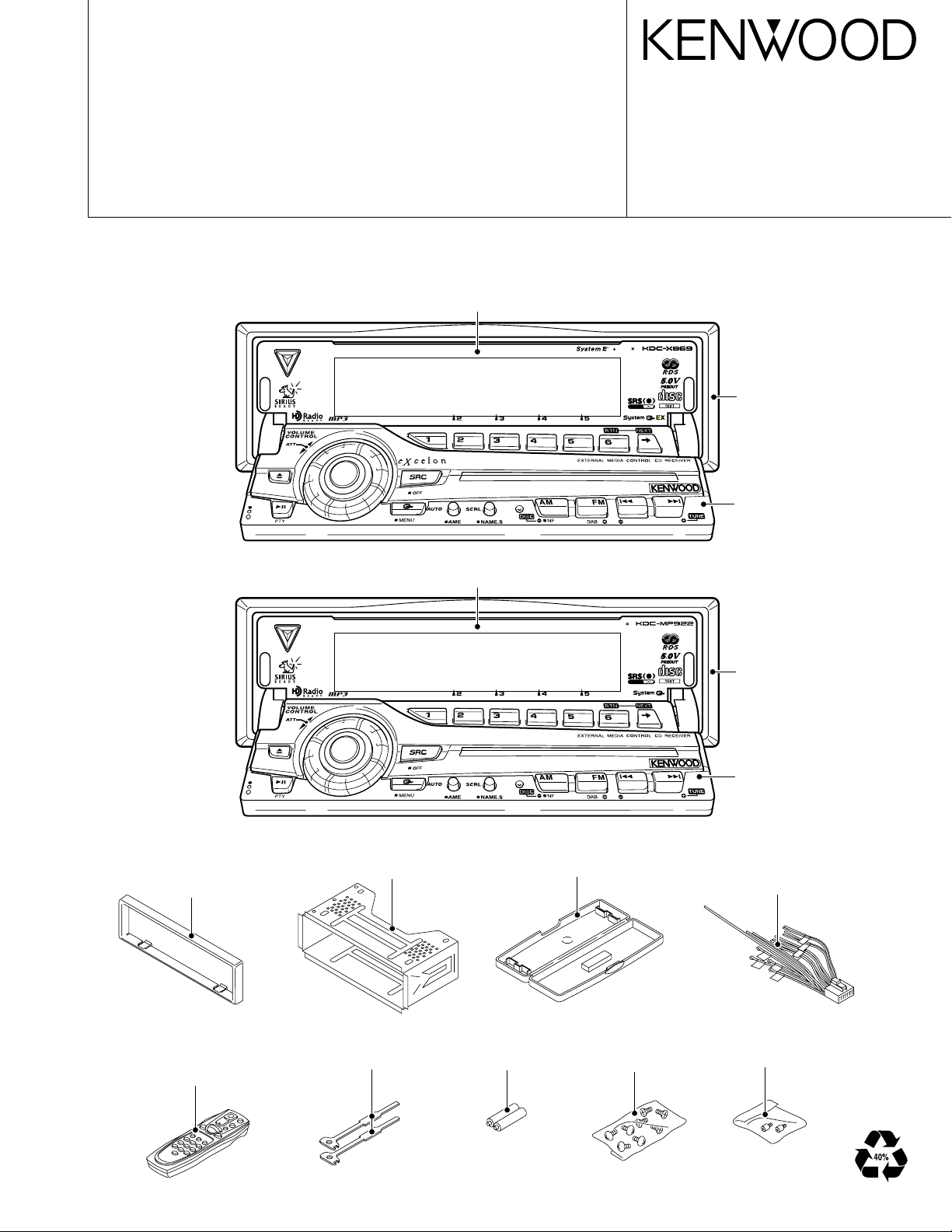
Panel assy
(A64-2976-01): KDC-X869
Panel assy
(A64-2977-01): KDC-MP922
CD mechanism extension cord : W05-0935-00
50 4W
s
COMPACT
DIGITAL AUDIO
50 4W
COMPACT
DIGITAL AUDIO
Escutcheon
(B07-3079-01):
KDC-X869
Panel assy
(A64-2993-02):
KDC-X869
Escutcheon
(B07-3078-01):
KDC-MP922
Escutcheon
(B07-3078-01) : KDC-MP922
(B07-3079-01) : KDC-X869
Remote controller assy
(RC-505)
(A70-2040-05)
Mounting hardware assy
(J21-9823-03)
Lever
(D10-4674-04) x 2
Plastic cabinet assy
(A02-2731-03)
Size AA battery
(Not supplied)
Screw set
(N99-1723-05)
Panel assy
(A64-2994-02):
KDC-MP922
DC cord
(E30-6062-05) : KDC-X869
(E30-6106-05) : KDC-MP922
Screw set
(N99-1734-05)
KDC-MP922/X869
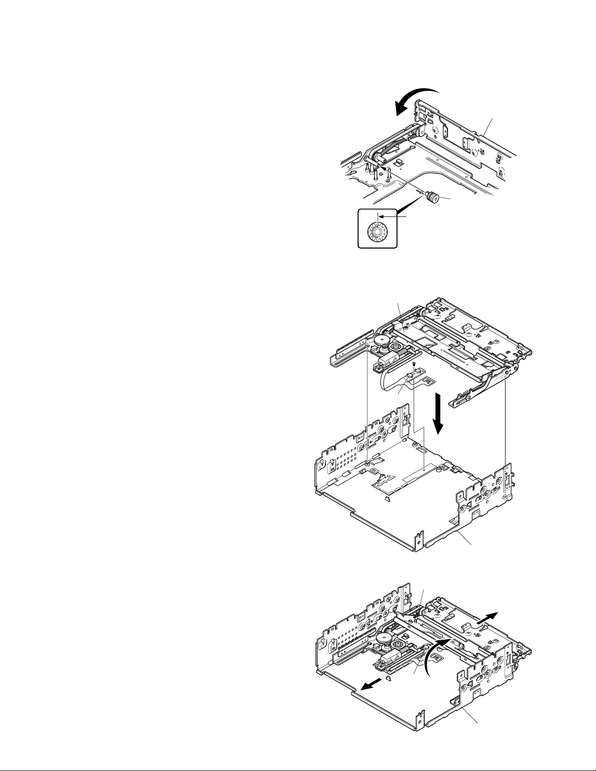
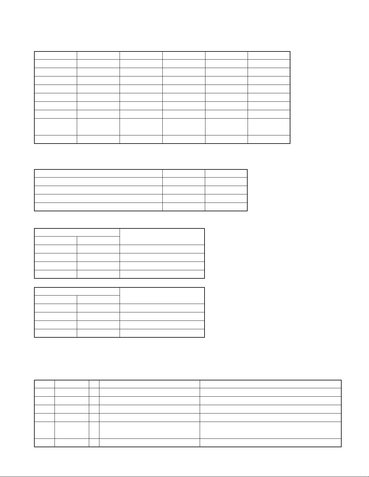
HOW TO THE PANEL MECHANISM ASSEMBLY
1. Fixed the position of operation side
(Fixed the horizontal position when the panel opened)
q The mounting hardware (281) of operation side is rota-
tion (A) into the stop position with close side.
w As figure (B) line is just above and the gear (230) at-
tached to pin.
2. The slider assembly insert to bottom chassis
q The bracket for display panel (284) is leave down, in-
sert to the chassis (702). (C)
A
Rotary to the
stop position
B
This line attached just above
Fig. B
(This figure from look at B arrow)
284
281
230
w The slider assembly insert to the chassis (702) after
that shift (D) direction.
e The bracket for display panel (284) is raised (E) direc-
tion.
r Keep the raising conditions, the slider assembly is shift
(F) direction.
(Note) Do not bend the knob of chassis detection switch
when the slider assembly insert.
SW
C
702
284
F
E
SW
D
702
3
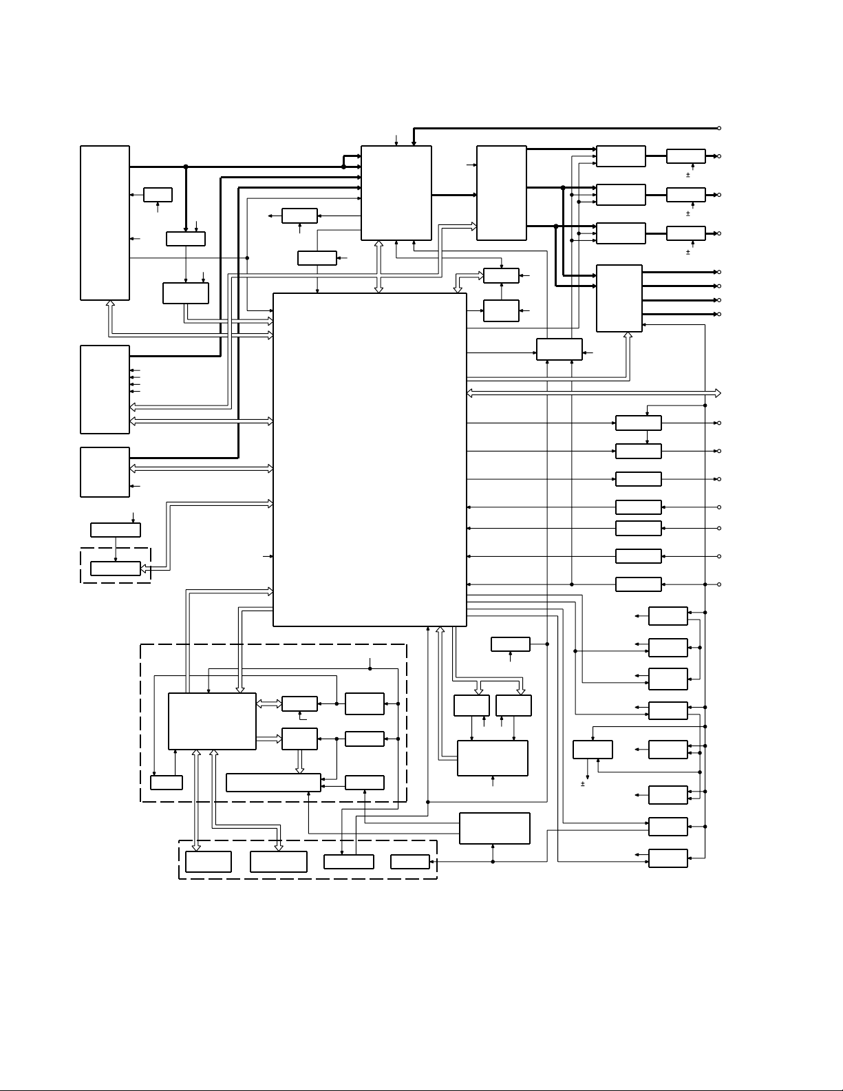
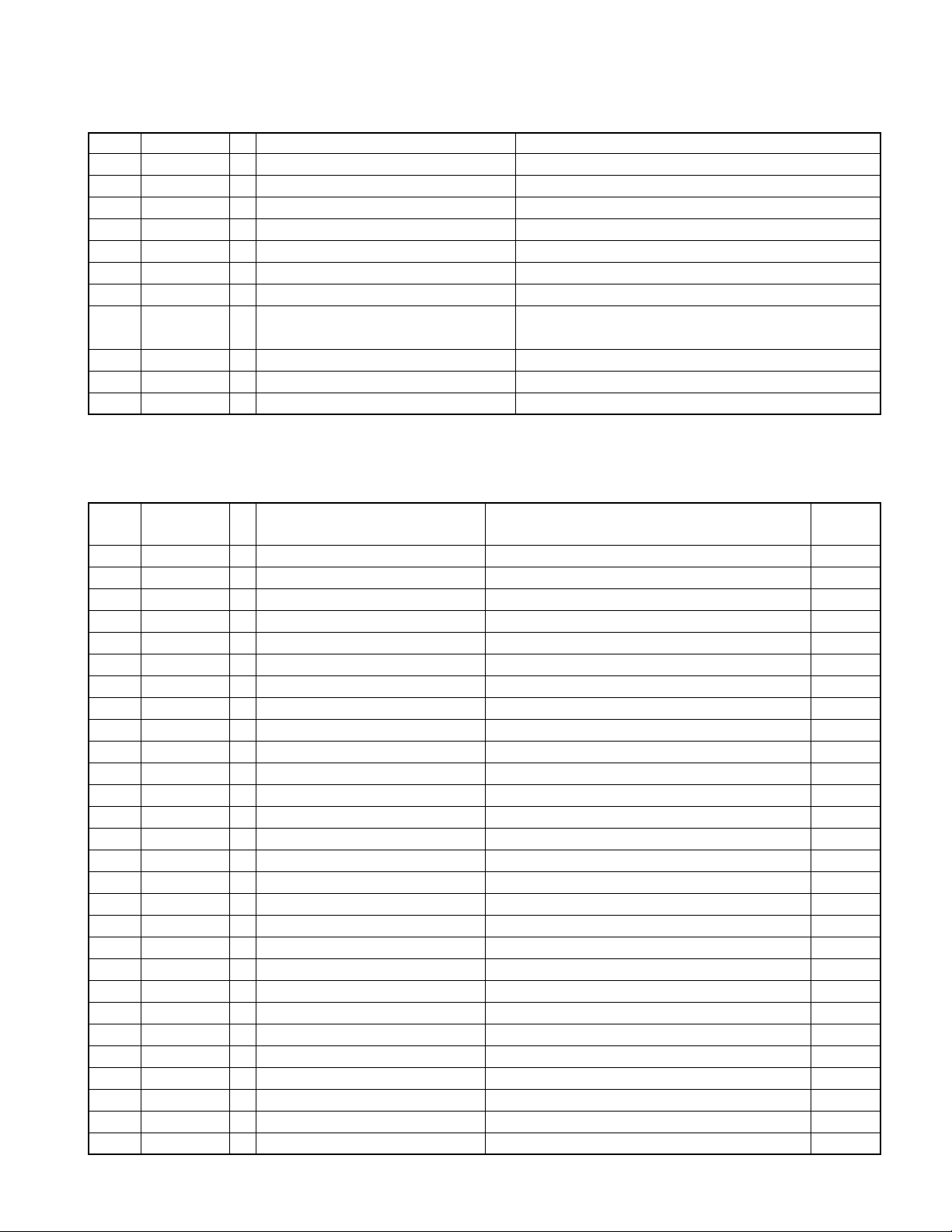
BLOCK DIAGRAM
KDC-MP922/X869
(X25-964)
TUNER
AUDIO OUT
S-METER
CD
CH
Q501
EEP5V
IC1
EEPROM
TDF UNIT
(X16-208)
Q303,304
AM+B
8V 8V
8V
BU5V
8V
SERVO
CD4.7V
BACK UP
BU5V
DISPLAY
UNIT
(X16-212)
REMO
IC9
SWITCH UNIT
(X16-217)
BUFFER
IC14
RDS
DECODER
IC11
ROT ARY
ENCODER
SW5V
u-COM
BPF
BU5V
FL
KEY MATRIX
IC1
KEY
AGC
IC10
BPF
LEVEL
SHIFT
8V
BUFFER
AGC
SW5V
PANEL5
Q6,10
PANEL
SW5V
Q4
FL3.3V
Q2,3
FL+B
RESET SW
IC2
FM
AM
CD
CH
QUAL
u-COM
8V
E-VOL
&
MPX
KEY ILL
8V
IC15
MOTOR
FL+B
FAC
IC5
SYSTEM
E'S+
WOW
IC20
FOCUS
SW
IC8
RESET
IC16
SERVO
PANEL
MECHA
SW5V
DC/DC
IC6
BU5V
MOTOR
DRDR
IC9
8V
8V
MUTE
DRIVER
Q207,208
PRE MUTE
Q203,204
PRE MUTE
Q205,206
PRE MUTE
IC4
POWER
IC
BU5V
IC18
Q23,24
ANT-CON ANT CON
Q25
EXT AMP
Q26
DIMMER DIMMER
TEL MUTE
Q29
ACC DET
Q27
B.U DET
BU5V
SW5V
PANEL5V
SW14V
DC/DC A8V
9V
SERVO
CD4.7V
IC13
IC12
IC11
P-CON P CON
Q1,2
BU5V
Q3,601
SW 5V
Q502,503
PANEL
5V
Q4,5
SW 14V
Q6-8
A8V
Q9,602
SERVO
Q11-14
FL+B
IC19
SW REG
OP AMP
9V
OP AMP
9V
OP AMP
9V
AUX IN
PRE OUT
(NF)
PRE OUT
(REAR)
PRE OUT
(FRONT)
SP OUT (FL)
SP OUT (FR)
SP OUT (RL)
SP OUT (RR)
WIRED REMO/
OPEL DISP I/F
EXT.AMP.CON
TEL MUTE
ACC
BACK UP
3
KDC-MP922/X869
COMPONENTS DESCRIPTION
● SUB-CIRCUIT UNIT (X16-2080-10)
Ref. No. Application/Function Operation/Condition/Compatibility
IC1 E2PROM For security
● SUB-CIRCUIT UNIT (X16-2120-10)
Ref. No. Application/Function Operation/Condition/Compatibility
IC1 3.3V regulator The power supply of IC and VFD (Logic) which are driven by 3.3V
IC2 Buffer IC It is change into 3.3V from 5V
IC3 Remote control IC
IC4 Spectrum analyzer IC
IC5 Panel µ-com
Q1, 2 FL+B SW FL+B (VDD2) is turned on when Q2’s base level goes “H”
Q3 REMO ON SW The power supply of IC2 and IC3 is turned on when Q3’s base level goes “L”
Q4 FL BLK SW VFD is turned on when Q4’s base level goes “H”
Q5 Blue LED SW Blue LED is turned on when Q5’s base level goes “H”
● SWITCH UNIT (X16-2170-10)
Ref. No. Application/Function Operation/Condition/Compatibility
Q1 DSI (Disabled System Indicator) DSI blinks when the base goes “H/L”
Q2 KEY illumination SW (GREEN) ON (KEY illumination green) when the base goes “H”
Q3 KEY illumination SW (RED) ON (KEY illumination red) when the base goes “H”
● ELECTRIC UNIT (X25-9640-1x)
Ref. No. Application/Function Operation/Condition/Compatibility
IC1 System µ-com
IC2 E-vol & N.C. & MPX
IC3 Regulator IC for A8V
IC4 Power IC
IC5 System E’s IC
IC6 Audio IC (WOW)
IC7
IC8 Reset IC
IC9 Logic IC for muting
IC10 Buffer for S.A
IC11~13 AMP for 4.5V Pre-out
IC14 RDS dcoder IC
IC15, 16
IC17 ROM IC For ROM correction.
-9V AVR (DC/DC IC) for 4.5V Pre-out
Motor driver IC for panel mechanism
4
KDC-MP922/X869
COMPONENTS DESCRIPTION
Ref. No. Application/Function Operation/Condition/Compatibility
IC18 P-CON IC
IC19 Swiching regulator IC for CD4.7V
IC20 Analog SW for swiching IC6’focus
Q1, 2 B.U.5V AVR While BU is applied, BU5V AVR outputs +5V.
Q3, 601 SW5V When Q601’base goes Hi, SW5V outputs +5V.
Q4, 5 SW14V When Q5’base goes Hi, SW14V outputs 14V.
Q6~8 AUDIO 8V AVR When Q6’base goes Hi, A8V AVR outputs 8.3V.
Q9, 602 SERVO+B AVR When Q602’base goes Hi, S+B AVR outputs 7.5V.
Q11~14 ILL&DC/DC+B AVR When Q11’base goes Hi, AVR outputs 9.2V.
Q15, 16 AUDIO 10.5V AVR When Q16’base goes Hi, AVR outputs 10.5V.
Q17~19 Pre-Amp -9V AVR
Q20~22 Pre-Amp +9V AVR
Q23, 24 P-ANT SW When Q23’base goes Hi, P-ANT SW outputs 14V.
Q25 Ex amp control buffer
Q26 Small lamp det SW When Q26’base goes Hi, Q26 is turned on.
Q27 BU det When Q27’base gose Hi, Q27 is turned on.
Q29 ACC det When Q29’base gose Hi, Q29 is turned on.
Q30, 31 Mute driver When a base gose Lo, mute driver is turned on.
Q201 Noise buffer
Q202 E-vol mute SW When a base gose Hi, mute SW is turned on.
Q203~208 Pre-out mute SW When a base gose Hi, Pre-out is muted.
Q210 AGC for SA
Q303, 304 AM+B SW When Q303’base gose Hi, AM+B is out.
Q305 Composite signal buffer for RDS
Q501 E2P 5V SW When Q501’base gose Lo, E2P 5V is out.
Q502, 503 PANEL 5V SW When Q503’base gose Hi, PANEL 5V is out.
Q603 SW for IC20 When Q603’base gose Hi, Q603 is turned on.
Q18 and 19 works as a differential amplifier, Q17 works as a driver and -9.1V is supplied
to OP amp for Pre-out.
Q20 and 22 works as a differential amplifier, Q21 works as a driver and +9.4V is supplied
to OP amp for Pre-out.
5
KDC-MP922/X869
MICROCOMPUTER’S TERMINAL DESCRIPTION
● SYSTEM MICROCOMPUTER : 703033BGC020 (X25-964 : IC1)
Pin No.
1 PLL_DATA I/O Tuner Data output/input with F/E.
2 AM+B I/O
3 (FM+B) O
4
5
6 EVDD 7 EVSS 8 AFS O Tuner Noise detection time constant switching.
9 BEEP O Audio Beep output.
10 REMO I Extra
11 P_MUTE O Audio Power IC MUTE output. Power OFF : L, All OFF : L, TEL mute : L
12 (SVR) O Audio Power IC SVR discharge circuit control.
13 IC2_SDA I/O Audio IC2, IC5 data line.
14 IC2_CLK I/O Audio IC2, IC5 clock line.
15 P_STBY O Audio Power IC STBY output.
16 P_CON I/O Extra Power control.
17 WOW_MODE2 O Audio WOW control. q
18 TEST - Connect to GND.
19 DIAG I Extra
20 MUTE O Audio Mute output. ON : OPEN, OFF : L
21 PRE_MUTER O Audio PREOUT (R ch) mute.
22 PRE_MUTEL O Audio PREOUT (L ch) mute.
23 BU_DET I Extra Momentary power dropped detection.
24 ACC_DET I Extra ACC detection. With ACC : L, Without ACC : H
25 FOCUS I/O Audio WOW focus control. Focus HI : H, Focus LOW : Hi-Z
26
27 DIMMER I Extra Small lamp detection. ON : L, OFF : H
28
29 P_ON I/O
30 ILL_ON I/O
31 RESET 32 XT1 - Sub clock. 32.768kHz
6
Pin Name I/O Module Purpose / Description
Power supply
Power supply
V_ILL PAN_E2P DATA
V_ILL PAN_E2P CLK
EXT_AMP_CONT
NC O NC (Without EXT_AMP_CONT model) Output : L
ANT_CON O Extra Antenna control. w
TYPE2 I Extra Destination select. w
I/O To panel
I/O To panel
CD CD mechanism data line.
Extra ROM correction data line.
CD CD mechanism clock line.
Extra ROM correction clock line.
O Extra External amplifier control. Refer to external amplifier control.
Power supply
Power supply
AM+B. AM operation : H
FM+B (S01 F/E only). FM operation : H,
V-ILL D/A converter (V-ILL, LCD), E2PROM data.
V-ILL D/A converter (V-ILL, LCD), E2PROM clock.
Remote control input (Panel, External display).
P_CONIC over voltage, over current detection.
SW 14V, SW 5V control, AD reference
voltage control output.
FL, illumination output. ON : H, OFF : Hi-Z
Truth table
Processing Operation
Last FM : H (With RDS, RBDS model)
FM seek, AF search : L, Receiving : H, Auto 0 : L
Power OFF momentary power dropped
: H (5 second) and then L
Power IC ON : H, Power IC OFF : L, All OFF : H
Power ON : H, Power OFF : Hi-Z, All OFF : Hi-Z
Usually : H, Unusually : L
M MUTE L is L : L (CD), Momentary power
dropped : L, 2 zone, NAVI interrupt : Fixed H
M MUTE R is L : L (CD), Momentary power
dropped : L, 2 zone, NAVI interrupt : Fixed H
Backup : L,
No backup, momentary power dropped : H
Tuner ON : H, Other source With RDS last FM
: H, Other source with RDBS TI ON last FM : H
K,J type (With ANT_CON model) : L,
E type (Without ANT_CON model) : H
Power ON : H, Power OFF : Hi-Z
KDC-MP922/X869
MICROCOMPUTER’S TERMINAL DESCRIPTION
Pin No.
33 XT2 - Sub clock. 32.768kHz
34 REGC - Connect to 1µF capacitor.
35 X2 - Main clock. 20MHz
36 X1 - Main clock. 20MHz
37 VSS 38 VDD 39 CLKOUT 40 LX_REQ_M O LX Communication request to external slave. Request : L
41 LX_MUTE I LX Mute request from external slave. Mute ON : H
42 LX_CON O LX External slave select. ON : H, OFF : L
43 LX_RST O LX Reset output to external slave µ-com
44 CD_MECHA+B O
45 TYPE0 I Extra Destination select. w
46 TYPE1 I Extra Destination select. w
47 IC2_TYPE0 I Extra IC2 destination. w
48 IC2_TYPE1 I Extra IC2 destination. w
49 PAN5V I/O
50 E2P5V I/O
51 DSI I/O To panel DSI control. ON : L, OFF : Hi-Z
52 MC_REQ O To panel Communication request to panel µ-com.
53 PAN_RST O To panel Reset output to panel µ-com.
54 WOW_MODE3 O Audio WOW control. q
55 BVDD 56 BVSS 57 SC_CON O To panel Panel µ-com control. Power OFF, ACC OFF : L
58 M_RST O CD Reset output to CD mechanism.
59 M_STOP O CD Stop request to CD mechanism. Stop : L, CD : H
60 CD_SW3 I CD DC down switch detection. Chucking : H
61 LO/EJ I/O CD CD mechanism loading/eject switch. Stop, brake : Hi-Z, Loading : L, Eject : H
62 MOSW O CD CD mechanism motor driver switch. Loading, eject, brake : H
63 FPM MOTOR B O P-mecha FPM mechanism (Slider) control. e
64 FPM MOTOR F O P-mecha FPM mechanism (Slider) control. e
65 FPM MOTOR O O P-mecha FPM mechanism (Angle) control. e
66 FPM MOTOR C O P-mecha FPM mechanism (Angle) control. e
67 NC O NC (Without external display model) Output : L
68 NC O NC (Without external display model) Output : L
69 NC O NC (Without external display model) Output : L
70 M_MUTER I CD Mute request form CD mechanism. (R ch). ON : L (CD)
71 AVDD 72 AVSS 73 AVREF - Connect to P_ON (29 pin).
74 M_MUTEL I CD Mute request form CD mechanism. (L ch). ON : L (CD)
75 PAN_DET I To panel Panel E2PROM detection. With : L, Without : H
76 NC I NC (Without TEL-MUTE model) Connect to GND.
Pin Name I/O Module Purpose / Description
Power supply
Power supply
Power supply
CD 4.7V output. ON : Fast 50ms than M_STOP,
Panel 5V control. ON : H, Momentary power dropped : Hi-Z
E2PROM, DA converter power supply control. ON : L, OFF : Hi-Z
Truth table
Processing Operation
Normally : L, After system reset : H (400ms
or more) and then L
CD source : H, Except CD source : L,
OFF : Slow 50ms than M_STOP
Normally : H, Reset, momentary power dropped : L
Normally : H, Reset : L (Per mechanism control)
7
KDC-MP922/X869
MICROCOMPUTER’S TERMINAL DESCRIPTION
Pin No.
77 FPM SW4 I P-mecha
78 FPM SW1 I P-mecha FPM mechanism position detection. e
79 FPM SW2 I P-mecha FPM mechanism position detection. e
80 FPM SW3 I P-mecha FPM mechanism position detection. e
81 FPM PHOUT I P-mecha FPM mechanism position detection. e H : 2.2V or more
82 S_METER I Tuner S-meter detection. Refer to S03 F/E control.
83 NOISE I Tuner FM noise detection. Refer to S03 F/E control.
84 IFC_OUT I Tuner F/E IFC OUT input.
85
86 NC O NC (Except J type) Output : L
87 R_CLK I Tuner RDS decoder clock input.
88 LX_REQ_S I LX Receive request from external slave. Request : L
89 SC_REQ I To panel Communication request from panel µ-com
90 CD_SW1 I CD Loading switch detection. Loading start power off : L
91 CD_SW2 I CD 12cm disc detection switch. 12cm disc power off : L
92 R_QUAL I Tuner RDS decoder QUAL input.
93 R_DAT A I Tuner RDS decoder data input.
94 LX_DATA_S I LX Data input from external slave.
95 LX_DATA_M O LX Data output to external slave.
96 LX_CLK I/O LX Clock input/output with external slave.
97 PAN_RX I To panel Data input from panel µ-com
98 PAN_TX O T o panel Data output to panel µ-com
99 WOW_MODE1 O Audio WOW control. q
100 PLL_CLK I/O Tuner Clock input/output with F/E.
Pin Name I/O Module Purpose / Description
FPM mechanism position detection,
mechanism detection. 1.25V or more : H, Less than 1.25V : L
NC (POWER_DET)
I Extra Power IC DC offset detection. 03 model not used. Connect to GND.
Truth table
e
Processing Operation
3.75V or more : No mechanism,
With station : 2.5V or more, refer to S03 F/E control.
Truth table
q WOW MODE changover operation
MODE WOW_MODE1 WOW_MODE2 WOW_MODE3 FOCUS
BYPASS L L L Don’t care
TruBass L H L Don’t care
3D-STEREO L L H Don’t care
FOCUS LOW H L L L (Hi-z)
FOCUS HI H L L H
WOW LOW H H H L (Hi-z)
WOW HI H H H H
w Destination port
MODEL Destination DISPLAY TYPE2 TYPE1 TYPE0
KDC-X969 K FL 0 0 0
KDC-MP922 K FL 0 0 1
FX-9000 J FL 0 1 0
KDC-PSW9524 E FL 1 0 0
KDC-9023R M (E) FL 1 0 1
KDC-X869 K FL 0 1 1
8
KDC-MP922/X869
MICROCOMPUTER’S TERMINAL DESCRIPTION
MODEL Destination DISPLAY TYPE2 TYPE1 TYPE0
KDC-8024 E FL - - KDC-MP822 K LCD - 0 0
KDC-M7024 E LCD - 0 1
FX-5000 J LCD - 1 0
KDC-V7022 K LCD 0 0 0
KDC-X769 K LCD 0 0 1
KDC-722 K LCD 0 1 0
KDC-7024
KDC-7024Y
KDC-8023 M (K) LCD 1 0 0
Note : When FL model using TYPE2, K & J type (with ANT_CON model) : L, E type (without ANT_CON model) : H
Destination(IC2)
Market model L L
Market model CRSC modiification L H
OEM model CRSC modification H L
OEM model CRSC and de-emphasis modification H H
E LCD 0 1 1
TYPE0 TYPE1
e FPM MOTOR
Slide
FPM MOTOR B FPM MOTOR F
0 0 Standby
1 0 Backward operation
0 1 Forward operation
1 1 Brake
Angle
FPM MOTOR O FPM MOTOR C
0 0 Standby
1 0 Angle open direction
0 1 Angle close direction
1 1 Brake
FPM mechanism operation
FPM mechanism operation
● PANEL MICROCOMPUTER 703032BGFA01 (X16-212 : IC5)
Pin No. Pin Name I/O Purpose / Description Procesing Operation
1 FL DATA1 O Data output to FL driver.
2 FL CLK O Clock output to FL driver. Communication speed : 2.5MHz
3 NC O Output : L
4 FL DATA2 O Data output to FL driver.
5 CLK IN I Serial clock input.
6 SYS TX I Data input from system µ-com.
Connect to 2 pin (Reset, low current consumption mode
: FL CLK output “L”).
(Reset, low current consumption mode : System µ-com output “L”)
9

KDC-MP922/X869
MICROCOMPUTER’S TERMINAL DESCRIPTION
Pin No. Pin Name I/O Purpose / Description Procesing Operation
7 SYS RX O Data output to system µ-com. Communication speed : 1.25Mbps
8 NC O Output : L
9 Evdd - PAN 5V
10 Evss - Vss
11~13 NC O Output : L
14 FL LATCH O Latch output to FL driver.
15 FL GCP O Bright control.
16~19 NC O Output : L
20 FL BLK O Display switching signal output to FL driver. H : Display ON, L : Display OFF
21 TEST I Connect to GND.
22~25 NC O Output : L
26~29 KS1~KS4 I/O Key scan. Key scan (Hi-Z/L)
30 REMO ON I/O Remote control IC power on/off. Hi-Z : OFF, L : ON (Time constant check, 500µs)
31 BLUE LED O Blue LED ON/OFF. H : ON, L : OFF
32 RED LED O Illumination red changeover. H : ON, L : OFF
33 GREEN LED O Illumination green changeover. H : ON, L : OFF
34 RESET I Reset. L : Reset, H : Reset cancel
35 TX1 36 TX2 37 REGC - Connect to 1µF capacitor.
38 X1 - Main clock. 20MHz
39 X2 - Main clock. 20MHz
40 Vss - Vss
41 VDD - Vdd
42 CLKOUT 43~47 NC O Output : L
48 FL+3.3V O FL3.3V ON/OFF. Hi-Z : OFF, L : ON (Time constant check, 1ms)
49 FL+B I/O FL+B ON/OFF. Hi-Z : OFF, L : ON (Time constant check, 35µs)
50~57 NC O Output : L
58 Vdd - Vdd
59 Vss - Vss
60~69 NC O Output : L
70 VOLUME B I VOL input.
71 VOLUME A I VOL input.
72 SA RST O Spectrum analyzer IC reset. H : reset, L : Normally
73 AV CONT O VREF control. Operation : H
74 Avdd - Vdd
75 Avss - Vss
76 Avref - Connect to 73 pin.
77 F01 I BPF (63Hz)
78 F02 I BPF (150Hz)
79 F03 I BPF (330Hz)
80 F04 I BPF (1kHz)
81 F05 I BPF (3.3kHz)
82 F06 I BPF (10kHz)
83 WAVE IN I Audio input.
10
KDC-MP922/X869
MICROCOMPUTER’S TERMINAL DESCRIPTION
Pin No. Pin Name I/O Purpose / Description Procesing Operation
84~88 KR5~KR1 I Key return.
89 SC REQ O Communication request to system µ-com. H : Request
90 NC(FAC IN) O Output : L
91 SC CON I Panel µ-com control. H : Operation
92 OPEN KEY I OPEN key input. H : OFF, L : ON
93 SRC KEY I SRC key input. H : OFF, L : ON
94 NC O Output : L
95 MC REQ I Communication request from system µ-com.
96 NC O Output : L
97~99 NC O Output : L (Flash µ-com writing port)
100 NC O Output : L
● MECHANISM MICROCOMPUTER : 703033BYGC-J02 (X32-541 : IC7)
Pin No. Pin Name I/O Use Processing Operation
1 NC O Not used. Fixed Low Low
2 E2P_SCL O ROM correction E2P IC2 clock. Hi-Z
3~5 NC O Not used. Fixed Low Low
6 VDD - 5V
7 GND - GND
8, 9 NC O Not used. Fixed Low Low
10 PON O Power ON/OFF control. H : ON, L : OFF Low
11 /PON O Power ON/OFF control. H : OFF, L : ON High
12
13 8EjE_SW I Not used. Fixed Low Hi-Z
14 LOS_SW I Not used. Fixed Low Hi-Z
15 12EjE_SW I Not used. Fixed Low Hi-Z
16, 17 NC O Not used. Fixed Low Low
18 IC/Vpp - Write voltage (Flash). 19 MUTE_L O L ch audio mute control. L : Mute ON, H : Mute OFF Low
20 MUTE_R O R ch audio mute conrol. L : Mute ON, H : Mute OFF Low
21~25 NC O Not used. Fixed Low Low
26 EFLG I WMA error detection. H : Error, L : No error Hi-Z
27 WAIT I Wait control signal detection. Hi-Z
28 FOK I Focus condition detection. H : Focus OK, L : Focus NG Hi-Z
29, 30 NC O Not used. Fixed Low Low
31 RESET I Reset detection. H : Normal, L : Reset Hi-Z
32 XT1 I Not used. Hi-Z
33 XT2 - Not used. 34 REGC 35 X2 36 X1 I Hi-Z
37 Vss - GND
LOE/LIM_SW
I Down limit switch detection. L : Most Inner position detection Hi-Z
H : Request (Reset, low current consumption mode
: System µ-com output “L”)
STBY
Processing
11

KDC-MP922/X869
MICROCOMPUTER’S TERMINAL DESCRIPTION
Pin No. Pin Name I/O Use Processing Operation
38 VDD - 5V
39 NC O NC Output stop. Low
40 WRL O Multiplex WRITE signal. _LBEN : 61002 (Not used), _WRL : 63760 Out-Low
41 NC O Not used. Fixed Low Low
42 R/W O Multiplex _R/W signal _R/W : 61002, _WRH : 63760 (Not used) Out-Low
43 DSTB,RD O Multiplex DSTB or RD signal _DSTB : 61002, _RD : 63760 Out-Low
44 ASTB O Multiplex ASTB signal Out-Low
45, 46 NC O Not used. Fixed Low Low
47~54 AD0~AD7 I/O Multiplex address/data Out-Low
55 BVdd - Bus interface power supply.
56 BVss - Bus interface GND.
57~64 AD8~AD15 I/O Multiplex data/address Out-Low
65 /HCSB O Chip select control. H : OFF, L : ON Low
66 /CS O Chip select control. H : OFF, L : ON Low
67 DSP RESET O DSP reset control. H : Normal. L : Reset Low
68 REQ I Data transfer request input. Hi-Z
69 DBBWRDY0 I DBB00 register write permission input. Hi-Z
70 DBBRRDY0 I DBB00 register read permission input. Hi-Z
71 Avdd 72 Avss 73 Avref I A/D port reference voltage input.
74 WTS I WMA table select. H : WMA8 table, L : WMA9 table Hi-Z
75 MDL_SEL I Model port changeover. H : 03 model, L : 02 model Hi-Z
76, 77 NC I Not used. Fixed Low Hi-Z
78 HOT I Temperature rise detection. Detection voltage : 4V, Reset voltage 3.9V Hi-Z
79 NC I Not used. Fixed Low Hi-Z
80 WMA I WMA correspond changeover. H : DXM6500 (With WMA), L : DXM6400 (Without WMA) Hi-Z
81 NC I Not used. Hi-Z
82 ASEL I Audio output pole changeover. H : Invert output, L : Normal output Hi-Z
83 DASC I Shock proof changeover. H : Shock proof OFF, L : Shock proof ON Hi-Z
84 E2P_WR I E2PROM write changeover. H : E2PROM write, L : Normal Hi-Z
85 PIC_SEL I PICK UP changeover. H : KPC6C, L : KSS710 Hi-Z
86 NC O Not used. Fixed Low Low
87 MSTOP I Standby restart interrupt. H : Standby, L: Stop
88 INTSV I Servo IC interrupt. H : Interrupt Hi-Z
89 FOGUP I Focus gain up interrupt. H : Focus gain up, L : Normal Hi-Z
90 ZMUTE_R I 0 bit mute detection. H : Mute ON, L : Mute OFF Hi-Z
91 ZMUTE_L I 0 bit mute detection. H : Mute ON, L : Mute OFF Hi-Z
92 NC O Not used. Fixed Low Low
93 D-MUTE O Driver mute. H : OFF, L : ON Low
94 SYS_SDA I/O System µ-com I2C data. Hi-Z
95 NC O Not used. Fixed Low Low
96 SYS_SCL I/O System µ-com I2C clock. Hi-Z
97~99 NC O Not used. Fixed Low Low
100 E2P_SDA O ROM correction E2P I2C data. Hi-Z
STBY
Processing
Hi-Z (Low input)
12

TEST MODE
KDC-MP922/X869
● How to enter the test mode
While pressing and holding the Preset 1 and Preset 3 keys,
reset the unit.
● How to exit from the test mode
While holding the Preset 6 key, reset the unit.
(Note) The test mode cannot be terminated by reset the
unit, ACC OFF, power OFF and Panel detached, momentary power down.
● Initial status in the test mode
• Sources : ALL OFF
• Display : All segments are lit.
• Volume : -10 dB (displayed as “30” )
• Loudness : OFF
• CRSC : OFF regardless of the presence of switching function.
• SYSTEM Q : Flat
• WOW : All OFF
• BEEP : When pressing any keys, the buzzer generates a
beep at any time.
• AUX : ON
• MENU SYSTEM Q : OFF
• Variable model : Default is white
• Multifunction : Source dependency (Preset, SCAN, etc.)
● Special display in Tuner mode
When any of the following messages is displayed in Tuner
mode, the F/E may be abnormal.
• “TNE2P NG” : The EEPROM is set to the default (unstable
values) because the F/E was shipped without passing
through the adjustment process, etc.
• “TNCON NG” : Communication with the F/E is not possib le .
● Forced switching of K3I
Each press of the Preset 6 key in Tuner mode should switch
K3I from AUT O → F orced Wide → F orced Middle → Forced
Narrow → AUTO.
The initial status is AUTO and the display shows these
modes as follows.
• AUTO : FMA
• Forced Wide : FMW
• Forced Middle : FMM
• Forced Narrow : FMN
● Test mode specifications of the CD receiver
• Forced ejection is inhibited in the reset start operation. When
the unit is reset while a CD is loaded in it, the CD is not
recognized by resetting.
• Each press of the Track Up ke y jumps to the f ollowing track
numbers:
No. 9 → No. 15 → No. 10 → No. 11 → No. 12 → No. 13 →
No. 22 → No. 14 → No. 9 (The cycle restarts from here.)
• Each press of the Track Down key jumps to the previous
track number to the track being played.
• When the number of total trucks of the MP3 disc or the
WMA disc is less than 9, 1st truck is played.
• When the disc media is CD, A short press of the Preset 1
key jumps to the track number 28.
• When the model is equipped the CD mechanism assembly
adapted for MP3 or MP3/WMA disc , the mechanism name
and version number are displayed during the FL model is
lower stand and Display mode of LCD model is DNPS.
● Audio-related specifications
• Pressing the ✽ k ey on the remote initiates the audio adjustment mode.
• BL/F key on the Fader initials.
• Continuous holding of a remote control key is inhibited, and
workings are short press of any keys.
• Bass, Middle and Treble are adjusted in 3 steps of -8 / 0 /
+8 with the Track Up/Down keys (Default value at 0).
• Balance is adjusted in 3 steps of L15 / 0 / R15 with the
Track Up/Down keys (Default value at 0).
• Fader is adjusted in 3 steps of R15 / 0 / F15 with the Track
Up/Down keys (Default value at 0).
• HPF is adjusted in 2 steps of OFF / 170Hz (or 220Hz) with
the Track Up/Down keys (Default value at OFF).
• LPF is adjusted in 2 steps of OFF / 120Hz with the Track
Up/Down keys (Default value at OFF).
• Bass f, Bass Q, Bass EXT, Middle f, Middle Q and Treble f
are not dealt with by the audio adjust.
• The WOW key pass during the audio adjustment as following steps.
Order
q OFF OFF OFF SRS WOW OFF
w ON OFF OFF SRS T ruBass ON
e OFF LOW OFF FOCUS LOW
r OFF HIGH OFF FOCUS HIGH
t OFF OFF ON SRS ON
y ON HIGH ON SRS WOW HIGH
TruBass FOCUS SRS
Mod.
Display
13
KDC-MP922/X869
TEST MODE
● Menu-related specifications
• A short press of the Q key initiates the menu mode.
• Pressing the DNPP key on the remote initiates the Menu
mode.
• Continuous holding of a remote control key is inhibited, and
workings are short press of any keys.
• Contrast is adjusted in 3 steps of 0 / 5 / 10 with the Track
Up/Down keys (Default value at 5).
● Backup current measurement
When the unit is reset while ACC is OFF (i.e. by turning
Backup ON), the MUTE terminal goes OFF in 2 seconds in
place of 15 second. (The CD mechanism is not activ ated at
this time.)
● Special display when the display is all on
Pressing the Preset keys while the power is ALL OFF displays the following information.
[PRESET 1] Version display (8 digits, Month/Day/Hour/Minute)
(Display) SYS xxxxxxxx : System microcomputer
PAN xxxxxxxx : FL model only
MEM xxxxxxxx : 4 contrasts FL model only
[PRESET 2] Serial number display (8 digits)
(Display) SNo xxxxxxxx
[PRESET 3] Short press : View power ON time. (The All OFF
period is not counted.)
2 seconds long press/hold : Clear power ON time
at the power ON time displaying.
(Display) PonTim xxxxx Max. 60000 (hours)
[PRESET 4] Short press : Display CD operation time.
2 seconds long press/hold : Clear CD operation
time at the CD operation time displaying.
(Display) CDTim xxxxx Max. 60000 (hours)
[PRESET 5] Short press : Display CD ejection count.
2 seconds long press/hold : Clear CD ejection
count at the CD ejection count displaying.
(Display) EjeCnt xxxxx Max. 60000 (times)
[PRESET 6] Short press : Display Panel open/close count.
2 seconds long press/hold : Clear Panel open/close
count at the Panel open/close count.
(Display) PnCnt xxxxxx Max. 600000 (times)
FM key Display ROM collection version.
(Display) ROM R xxx Invalid : “R – – –”
AM key Display panel E2PROM condition.
(Display) P–ROM OK (Registered code)
P–ROM NG (Code is write in error)
P–ROM WAIT (Unregistered code)
P-ROM NON
(Panel security nonfunctional)
14
● Panel mechanism
• Auto-panel close inhibition when set-in the CD.
• The panel operation inhibition at power ON/OFF and ACC
ON/OFF.
• The panel position changing Eject ←→ Last with a short press
of the PLAY/PAUSE keys.
● Other specifications
• No displays such as “CODE OFF/ON” during Power-ON.
• The LINE MUTE inhibition time is one second from 10 seconds when start-up the test mode.
• Do not write the security code with the security jig on the
test mode.
• Do not write the serial with the serial writing jig on the test
mode.
• OEM display output is not stop if OEM display not connection on the test mode.
● Switching the frequency span (K/M type)
While holding the Preset 1 key and Preset 5 key, reset the
unit.
● Response to OEM setting
(Destination of electronic volume setting)
S03F/E models are response to OEM models option at put
in µ-com 2 pin.
Its setting are following steps.
IC2 TYPE0 IC2 TYPE1
(47 pin) (48 pin)
Low Low q T rade model (Initial quantify)
Low High w Trade model (CRSC change)
High Low e OEM model-ready CRSC change
High High
r OEM model-ready CRSC &
de-emphasis change
Description
● Security-related information
1. Forced Power ON mode (All models)
Even when the security (Cord) is approved, resetting the
unit while holding the Q and Preset 4 keys makes it possible to turn the power ON for 30 minutes.
After 30 minutes have elapsed, it is not possible to return to
the previous condition unless the unit is reset again. (Security code is do not clear at this mode. Put the power on fillin.)
 Loading...