

Kenwood KDC-X817, KDC-9017 Service Manual
CD RECEIVER
KDC-X917/X817/9017
SERVICE MANUAL
© 2001-1 PRINTED IN JAPAN
B51-7716-00(S) 1529
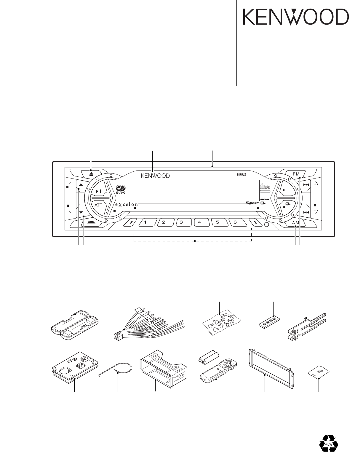
● KDC-X817
Knob(EJECT)
(K24-3653-04)
ANG
DISP
NAME
Front glass
(B10-3252-01:X917)
(B10-3253-01:X817)
(B10-3254-01:9017)
PTY
4.5V
PREOUT
CLK
LOUD
50Wx 4
SCANMENU RDM REP
Panel assy
(A64-2149-02:X917)
(A64-2150-02:X817)
(A64-2151-02:9017)
KDC-X817 System E's+
M. RDM
AUTO
COMPACT
DIGITAL AUDIO
TEXT
AME
OFF
SRC
EX
AUD
DISC
DAB
DISC
NF
Knob(VOL)
(K25-1216-03)
Plastic cabinet assy
(A02-1497-03)
Bracket
(J19-5051-03:L)
(J19-5052-03:R)
DC cord
(E30-4939-05:X917/X817)
(E30-4940-05:9017)
Torsion coil spring
(G01-2924-04)
Knob(1-6)
(K25-1221-03)
Mounting hardware assy
(J21-9716-03)
Screw set
(N99-1652-05)
Remote controller assy
(A70-0883-05:9017)
(A70-0894-05:X917/X817)
Knob(FM/AM)
(K25-1218-03)
Stay
(J54-0606-04)
Escutcheon
(B07-3010-02)
Lever
(D10-4562-04)
Screw set
(N99-1704-05)
KDC-X917/X817/9017
PLL+B
FM+B
AM+B
DIMMER
MUTE
2WAY
DET.
ACC
SRM
BU DET.
SRM
DRIVER
A8V
SERVO
DC/DC
SW5V
BU5V
P CON
ANT-CON
MUTE
DRIVER
4.5V PRE
MUTE
E's
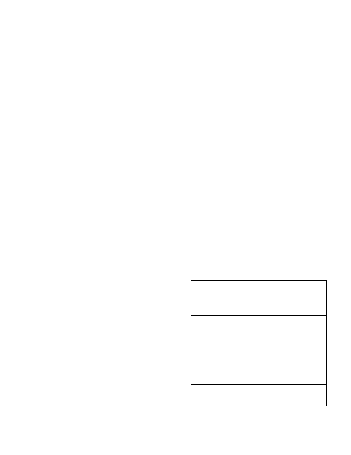
POWER IC
IC4
u-COM
IC1
CD
CH
IC7
IC10-12
Q37-42
IC5
IC2
F/E
MECHA
E-VOL
PRE OUT
SP-OUT
DIMMER
TEL-MUTE
ACC
ANT-CONT
P-CON
BACK UP
DECORDER
RDS
IC14
IC8
Q14
Q15
Q31
Q26-29
Q1,2Q3
Q51
Q9
Q30
IC15
IC2
IC1
IC3
EX.AMP CONTROL
AVR
DC/DC
BOX
PANEL u-COM
RESET
SW
RESET IC
VFD
(GRADATED)
REMO
G/R SW
SPEANA
IC16
BUFFER
Q36
NOISE
PRE OUT OUTPUT VOLTAGE
SPEANA
AGC OPAMP
CONTROL
EX.AMP
NAVI-MUTE
PANEL 5V
4.5VPRE
Q4-6
Q7,8
IC6
DC/DC
REG
KEY MATRIX
BFP
IF+B
SW14V
IC4
IC5
ROM
REG
3.3V
CH
S-METER
QUAL
SERVO+B
MUTE R
M STOP
SW2
LO/EJ
MUTE L
M RST
SW3
SW1
MS DATA
MS CLK
A8V
BU5V
SW5V
RST
REQ C
CLK
CH-CON
DATA H
REQ H
CD
AM
FM
MUTE
PRE MUTE
MC REQ
PANEL RST
SC REQ
MC CLK
SC DATA
MC DATA
RESET
SRM SW2
SRM SW3
SRM DET
SRM SW1
RDCK
RDDA
QUAL
SDA
SCL
AFS
AFS
S-METER
A8V
+B
-B
+B
-B
SCL
SDA
S-METER
SW5V
DATA C
BACK UP
PANEL 5V
PANEL 5V
FAC
FL+B
750mV
4500mV
CHANGER
AM
4.5V PRE
2250mVFM
230mV
1200mV
1200mV
251mV (E TYPE)
470mV (K TYPE)
IFC OUT
AUDIO OUT
SW5V
NOISE
IFC OUT
4500mVCD
K TYPEMODE
4500mV
4500mV
1069mV
1715mV
E TYPE
3600mV
600mV
1800mV
3600mV
K TYPE E TYPE
3600mV
1372mV
855mV
3600mV
1.8V PRE
SRM SUBSRM SUB+
DRIVER
MUTE
BU5V
MO SW
Q52
BUFF
FL(GRADATED) TYPE
(X13-994)
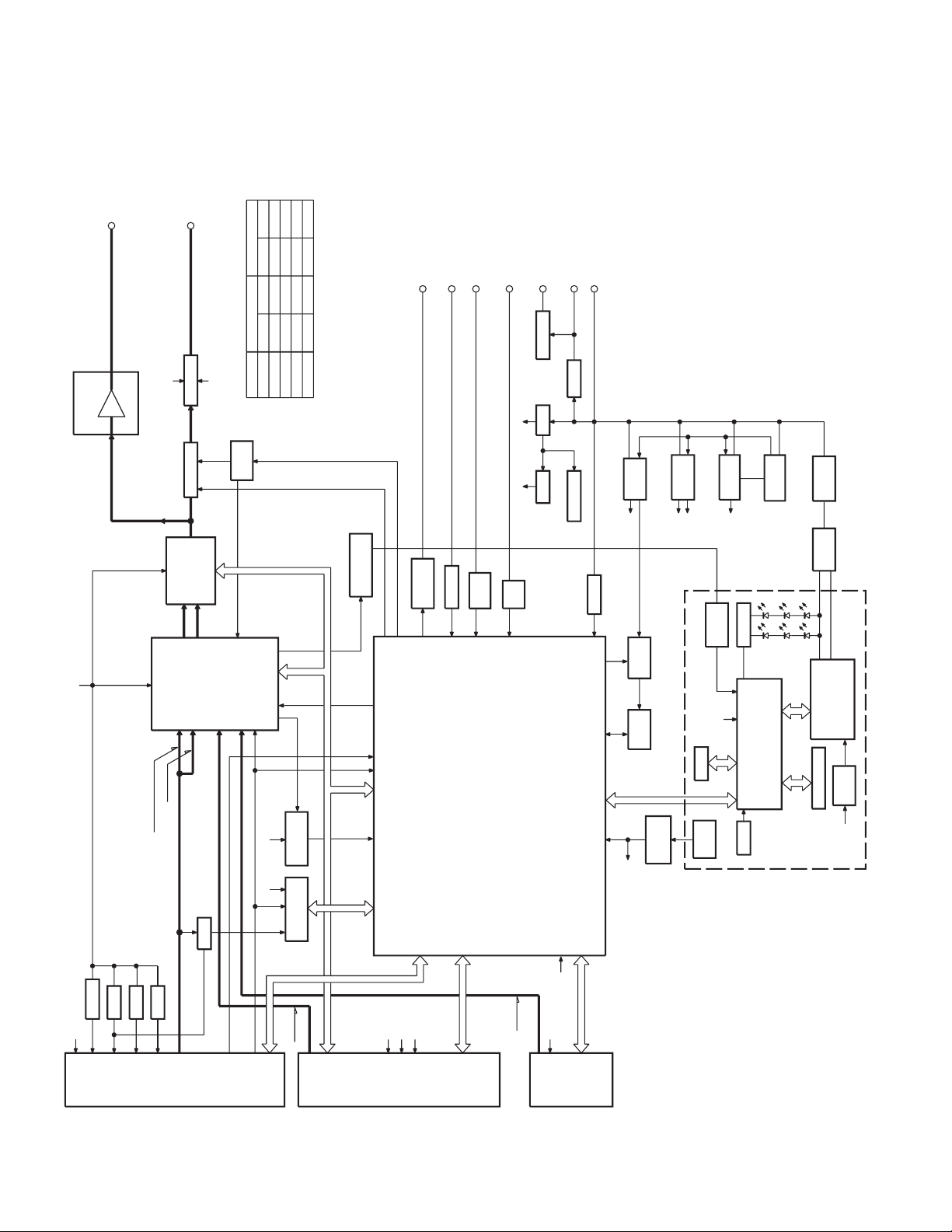
BLOCK DIAGRAM
2
KDC-X917/X817/9017
MICROCOMPUTER'S TERMINAL DESCRIPTION
System µ-com: UPD703033GC051
●Terminal description
Pin Function I/O Description Processing Operation
1 AM+B O AM power terminal H: During AM radio operation
2 FM+B O FM power terminal H: During FM radio operation
H: During FM radio operation if with RDS, RBDS
3
AFS
4 PLL-DATA I/O Data I/O terminal to F/E
5 PLL-CLK I/O CLK terminal to F/E
6 Evdd - Positive power terminal
7 Evss - GND terminal
8 N.C O Open (not used)
9 BEEP O BEEP output terminal
10 N.C O Open (not used)
11 PRE-MUTE L O L (during CD): when M MUTE L is L (low)
12 PRE-MUTE R O L (during CD): when M MUTE R is L (low)
13 IC2-SDA I/O IC2, IC5, CD mechanism, DATA line
14 IC2-SCL O IC2, IC5, CD mechanism, CLK line
15 N.C O Open (not used)
16 N.C O Open (not used)
17 N.C O Open (not used)
18 TEST - Test terminal
19 P-MUTE O Power IC MUTE terminal L: During Power-OFF L: During All-OFF
20 P-STBY O Power IC STBY terminal
21 MUTE O MUTE termianl ON: Open OFF: L
22 N.C O Open (not used)
23 N.C O Open (not used)
24 ACC-DET I ACC detection terminal L: ACC H: No ACC
25 DIMMER I Small detection terminal ON: L OFF: H
26 SW5V O 5 volt power terminal ON: L OFF: H
27 EXT-AMP-CO O External AMP control terminal (200ms) L 40ms: Bus boost OFF
28 P-CON O Power control terminal Power ON: H Power OFF: L
29 ANT-CON O Antenna control terminal TUNER, TI ON: H Open if no ANT-CON
30 P-ON O SW14V control terminal Power ON: H Power OFF: L
31
RESET
32 XT1 I Subclock terminal Time count Operation during Power-OFF
33 XT2 - Subclock terminal
34 REGC 35 X2 - Main clock terminal Oscillates: During Power-ON
36 X1 I Main clock terminal
37 Vss - GND terminal
38 Vdd - +B terminal
39 CLKOUT O Internal system clock output
40 N.C O Open (not used)
41 N.C O Open (not used)
42 TYPE0 I Destination selector port
43 TYPE1 I Destination selector port
44 TYPE2 I Destination selector port
45 N.C O Open (not used)
46 IC2TYPE0 I IC2 destination terminal L: During default
O Switching terminal for noise detection L: During AF search, FM seek
H: During receive
L during momentary power down
Fixed at H only during 2 zone
L during momentary power down
Fixed at H only during 2 zone
L: During Tell-mute
Power IC ON: H. Power IC OFF: L. During All-OFF: H
L 70ms: Bus boost LOW
L 100ms: Bus boost HI
I Reset IN terminal H: Normally H: During reset
Capacitor output terminal for regulator inside microprocessor
Oscillates stop: During Power-OFF, during
momentary power down
3
KDC-X917/X817/9017
MICROCOMPUTER'S TERMINAL DESCRIPTION
Pin Function I/O Description Processing Operation
47 IC2TYPE1 I IC2 destination terminal L: During default
48
CH-REQH
49 CH-RST O Reset output to changer Normally L, after system RST reset is ”H” for
50 CH-MUTE I Mute request from changer ON: H OFF: L
51 CH-CON O Changer control output ON: H OFF: L
52 ILL-ON O FL, illumination output ON: H OFF: L
53 M-MUTE L I Mute request from CD mechanism ON: L
54 M-MUTE R I Mute request from CD mechanism ON: L
55 BVdd - +B terminal
56 BVss - GND terminal
57 M-RST O Reset output to CD mechanism Normally H, L:During reset
58 M-STOP O Stop request to CD mechanism Stop: L H: During CD
59 N.C O Open (not used)
60 LO/EJ I/O CD mechanism, LODING, EJECT selector Stop, Brake: Hi-z, LOADING: L, EJECT: H
61 MOSW O CD mechanism, MOTOR, SW LOADING, EJECT, Brake: H
62 N.C O Open (not used)
63 CD-SW3 I CD down SW detection terminal Chucking: H
64 PAN-RESET O Reset output to panel microprocessor
65 MC-REQ/PAN I/O
66 N.C O Open (not used)
67 N.C O Open (not used)
68 N.C O Open (not used)
69 N.C O Open (not used)
70 AVCONT O AD reference voltage control output Same timing as P ON H: During operation
71 Avdd - +B terminal
72 Avss - GND terminal
73 Avref I
74 PHONE I PHONE detection terminal Tel mute: Min 1 volt, Navi mute: Max.2.5 volt
75 SRM-SW3 I Mask mechanism position detection input See 01mask mechanical position detection chart
76 SRM-SW1 I Mask mechanism position detection input See 01mask mechanical position detection chart
77 SRM-SW2 I Mask mechanism position detection input See 01mask mechanical position detection chart
78 SRM-DET I Mask mechanism detection input L: Mechanism H: No mechanism
79 NOISE I FM noise detection terminal
80 S-METER I S meter detection terminal
81 R-DATA I RDS DECODER DATA input terminal Connect to GND: On models without RDS,
82 R-QUAL I RDS DECODER QUAL input terminal Connect to GND: On models without RDS,
83 IFC-OUT I F/E IFC OUT input terminal L: When station present
84 N.C I Open (not used) Connect to GND
85 N.C I Open (not used) Connect to GND
86 SRM-B O SRM mechanical submotor output terminal
87 R-CLK I RDS DECODER CLK input terminal Connect to GHD: On models without RDS,
88 CH-REQC I Input request from changer ON: L
89 SC-REQ I
90 CD-SW1 I LOADING SW detection terminal LOADING start: L
91 CD-SW2 I 12cm disk detection switch terminal 12cm DISC: L
92 SRM+B O SRM mechanical submotor output terminal
93 BU-DET I Momentary power down detection terminal L: B.U H: No B.U (momentary power down)
94 CH-DATAC I Data input terminal from changer
95 CH-DATAH O Data input terminal to changer
96 CH-CLK I/O CLK I/O terminal used with changer
97 SC-DATA I Data line from panel microprocessor
98 MC-DATA I/O Data line to panel microprocessor
99 MC-CLK O CLK terminal to panel microprocessor
100 PAN5V O Panel 5 volt control terminal L: Panel H: No panel
O Request output to changer
REQ terminal/panel detection for panel microprocessor
Reference voltage supply terminal for A/D converter
Communication request from panel microprocessor
400ms and then ”L”
Per mechanical control specs.
Normally H, L: During reset, momentary power down
L: During panel use
RBDS
RBDS
RBDS
4
KDC-X917/X817/9017
ADJUSTMENT
Test Mode
1. How to enter test mode
While holding the FM key and the Preset 6 key, reset the
unit.
2. How to exit from test mode.
While holding down the Preset 6 key, reset the unit.
Note: Does not exit from test mode ACC-OFF, Power-OFF
or Momentary power down
3. Test mode reset status
•Sources are all OFF
•All display segment lit up
•Volume at -10dB (shows 30 on display)
•LOUD is OFF.
•CRSC is OFF regardless of whether switching function is
provided.
•SYSTEM Q is in FLAT
•Blank skip is OFF. (C/R model)
•LEDs are white, no scanning. (VLCD model)
4. Special displays in Tuner
When the following displays appear in tuner mode it shows
a problem with the front end.
•“TNE2P NG” ..... F/E is not aligned and EEPROM is in
reset (no settings) such as when shipped.
•“TNCON NG” .... Cannot communicate with F/E (front
end).
5. K3I switching
Each time the Preset 6 key is pressed in Tuner mode,
switches one at a time through the following sequence:
AUTO → Forced Wide → Forced Middle → Forced Narrow
→ AUTO. When reset, displays the following in AUTO.
•AUTO ................ FMA
•Forced Wide ..... FMW
•Forced Middle ... FMM
•Forced Narrow .. FMN
6. CD receiver test mode specifications
•No automatic ejection during reset-start. Does not make a
CD check in reset with a CD loaded.
•Using the Track up key jumps to the following tracks.
No.9→No.15→No.10→No.11→No.12→No.13→No.14→and
back to No. 9
•Using the Track down key moves 1 track downwards from
the track being played.
7. Audio items
•Momentarily pressing the Q key calls up audio adjustment
mode.
•Pressing the ∗ key on the remote control calls up audio
alignment mode.
•Continuous forward is disabled on the remote control.
•Bass/Middle/Treble are settable in 3 steps of MIN/
CENTER/MAX with the Track up/down keys.
•Balance is settable in 3 steps of Left MAX/CENTER/Right
MAX with the Track up/down keys.
•Fader is settable in 3 steps of Rear MAX/CENTER/Front
MAX with the Track up/down keys.
•HPF is settable in 2 steps of THRU/220Hz with the Track
up/down keys.
•LPF is settable in 2 steps of THRU/120Hz with the Track
up/down keys.
•Bass f/Bass Q/Bass EXT/Middle f/Middle Q/Treble f do
not appear in the audio alignment.
8. Menu items
•Momentarily pressing the CLK key calls up the Menu mode.
•The DNPP/SBF keys on the remote control calls up Menu
mode.
•Continuous forward is disabled on the remote control.
•Calendar adjust, calendar display switching and calendar
memo are eliminated from forward (FL model)
•In color alignment mode, Preset 1 is red, 2 is blue, 3 is
green and 4 is white. (VLCD model).
•Contrast is set in 3 steps of 0, 5, 10 and the reset value is
5. (VLCD/LCD models)
•Brightness adjustment is set in 3 steps of 0, 5, 10 and the
reset value is 10. (Normal FL model)
9. Backup current measurement
The MUTE terminal turns off 2 seconds (not 15 seconds)
after being reset in ACC off (backup on). (The panel, CD
and tape mechanisms are disabled during this time.)
10. Special displays during All-Off with all lamps on
The following displays appear when the preset keys are
pressed with all display segment lit up.
PRESET1 Version display (8 digits; Mo. Dy. Hr. Mn.)
(Display) SYS XXXXXXXX system microprocessor
PAN XXXXXXXX panel microprocessor
PRESET2
PRESET3
PRESET4 Press once: TAPE/CD/MD operating time display.
PRESET5 Press once: TAPE/CD/MD eject count display.
PRESET6 Press once: PANEL open/shut count display.
Serial No. display (8 digits) Note: CD/RK type eXcelon model
(Display) SNo XXXXXXXX
Press once: Power-on time display (Does not count during All-Off)
Press long: Clears the time display during power-on.
(Display) PonTim XXXXX (C/R) MAX 65535(time)
Press long: Clears TAPE/CD/MD operating time.
(Display) CDTime XXXXX (CD/R)
TapTim XXXXX (C/R) MAX 65535(time)
Press long: Clears TAPE/CD/MD eject count display.
(Display) EjeTim XXXXX MAX 65535(count)
Press long: Clears PANEL open/shut count display.
(Display) PnCnt XXXXX MAX 655350(count)
5

KDC-X917/X817/9017
ADJUSTMENT
11. Others
•Automatic panel close is disabled when tape or CD is
inserted. (M&T model)
•Panel operation is disabled at Power-ON or Power-OFF.
(M&T model)
•Panel open and closes with the ATT key. (M&T model)
•No displays such as “CODE OFF” during Power-ON.
•Pressing the TI (AUTO) key during changer operation turns
on 2zone. Cancel by pressing the TI (AUTO) key again.
The P/S dot is lit during 2zone.
•Pressing the CLK key for 1 second or more during All OFF,
calls up the Mask Key (security) write mode.
Security items
• Forced power-ON mode (all models)
Even when writing is permitted by the security function (mask
key), Power-on can be set for a 30 minute period each time
the reset key is pressed while holding down the ATT key
and Preset 4 keys. After 30 minutes elapses, can only be
restored by using reset.
• How to register the security code for EEPROM (F/E)
replacement (coded security models)
1. While holding the FM key and the preset 6 key, reset the
unit.
2. Call up security register mode by pressing the CLK key.
3. Enter the code with the Preset 1/2/3/4 keys.
For example, to enter the number, “3510”....
- Press the Preset 1 key 4 times.
- Press the Preset 2 key 6 times.
- Press the Preset 3 key 2 times.
- Press the Preset 4 key 1 time.
4. Hold down the DISP key for at least 3 seconds and the
message, “RE-ENTER” appears, so once again enter
the code according to Step 3 above.
5. Hold down the DISP key for at least 3 seconds, and the
message, “APPROVED” appears.
6. Cancel test mode. (See, 2. How to cancel the test mode.)
Note: All clear cannot be performed on the security code
for this model.
• Simple way to clear the security code (K type only)
1. During code request mode, press the VOL UP key for at
least 3 seconds while holding down the DISP key.
(---- will disappear)
2. Enter, “KCAR” with the remote controller as described
below. (Same as on 00 model.)
Press the remote controller 5 key twice, and press the
Track Up key. (Enters a “K”)
Press the remote controller 2 key three times, and press
the Track Up key. (Enters a “C”)
Press the remote controller 2 key once, and press the
6
Track Up key. (Enters an “A”)
Press the remote controller 7 key twice, and press the
Track Up key. (Enters an “R”)
3. Security function is canceled and unit sets to All-Off mode.
4. Code request mode appears if a mistake was made in
entering the numbers.
IHGE FDCA B
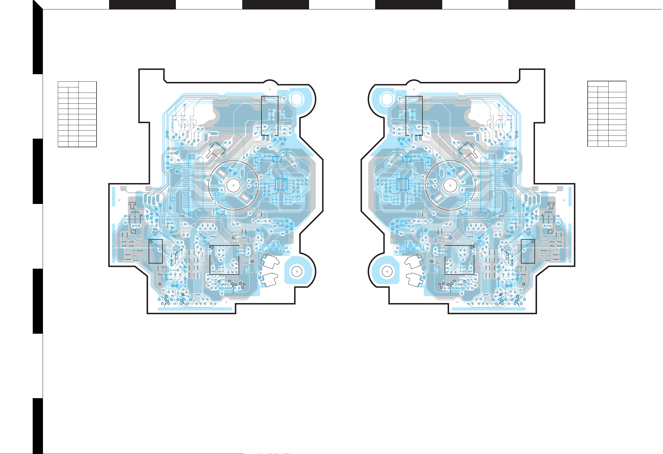
PC BOARD (Component Side View)
PC BOARD (Foil Side View)
1
CD PLAYER UNIT CD PLAYER UNIT
CD PLAYER UNIT
(X32-5030-00)
.ON.feR
CIQ
1B4
2C4
2
4D2
5D3
6D3
1B4
2D4
3D3
4C4
5D4
sserddA
3
D1
R8
C5
4
R10
R11
R12
C10
C11
5
FCS+
LD
R9
C4
W17
PD
B
E
C6
C7
C12
R5
Q1
CN1
1
C8
16
R202
IOP+
IOP-
/RFDET
X32-5030-00 (J74-1161-02)
R72
R83
C43
C45
R71
R73
R82
ECS
LOAD
SLED+
SW3
S.+B
TRK+
FCS-
VR
IC1
C89
TRCRS
GND
16
+
TRK-
32
17
C2
+
-
BDO
R3
C1
TE
FE
ARF
S.GND
A.+B
C18
C
C16
A
R234
+
TE
FOD
+
EJECT/SLED-
1
Rch
CP3
22
C3
R6
F
Vcc
Vc
1
R19
D
B
R17
TBAL
FBAL
GCTL
-
VDET
RF
LDON
F
TR
OFT
+
CN2
C19
C15
R233
E
R81
R75
TVD
A.GND
Lch
R47
C55
RW
D4
1
C35
R218
C20
C33
R21
R20
C14
R16C13
R15
R18
Vref
R32
25 51
C17
26
R34
TOFS
R36
C23
S3
CP2
CP1
C29
SPDL-
BE
Q4
CLVS
IC2
C85
R54
C24
C26
R37
C28
R38 C25
IPFLAG
/MSTOP
/MRST
C21
76100
X1
50
FCLK
FLAG
SPDL+
C46
BU.5V
75
DQSY
STLD
R76
R44 C51
Q3
R52
R213
LDCNT
SMCK
ST-O
14
R107
1
/MUTER
LO/EJ
EB
C34
R45
R125
R49
D.OUT
Q2
R46
S2
IC4
C41
R77
/MUTEL
C79
C77
C71
R121
R117
D2
EBEB
8
5
S1
IC5
I
C67
GO
R103
28
R78
15
A.5V
IC6
D3
SW2
D.GND
MOTOR
C63
+
C80
1
4
C72
C68
/RST
Q5
C78
R104
/CLK
SW1
R122
DAT A
R126
R118
R102
R108
R108
R102
DATA
/CLK
MOTOR
R126
R118
SW1
R122
/RST
C78
C72
+
C80
1
4
R104
D.GND
A.5V
C68
SW2
Q5
28
15
C63
D3
R78
IC5
GO
IC6
BBEE
X32-5030-00 (J74-1161-02)
1
IC4
C41
R77
/MUTEL
I
C79
8
5
C71
R103
D2
/MUTER
LO/EJ
C34
R45
C77
R121
C67
D.OUT
Q2
S1
14
R125
R117
R76
R44C51
EB
Q3
R107
R49
R46
S2
LDCNT
SMCK
ST-O
/MRST
SPDL+
BU.5V
R213
DQSY
STLD
/MSTOP
R52
C46
75
51
76
50
FCLK
SPDL-
C21
CLVS
X1
C24
C28
C25
FLAG
IPFLAG
IC2
R37
C85
R54
C26
R38
R72
R83
C43
R73
+
1
C19
C15
Rch
CN2
C3
FOD
S.GND
A.+B
Vcc
Vc
D
B
R17
TBAL
GCTL
RF
TR
R71
CP3
R6
F
1
R234
-+
TE
F
C45
TRK-
R3
C18
C
A
TE
FE
ARF
R82
ECS
+
LOAD
SLED+
SW3
S.+B
TRK+
FCS-
C1
16
32
17
C16
C2
+
-
TRCRS
BDO
/RFDET
FCS+
LD
VR
PD
R5
CN1
1
IC1
16
C89
R202
GND
IOP+
IOP-
D1
R8
R9
C4
W17
B
Q1
E
C5
R12
C6
R10
R11
C7
C8
C10
C12
C11
R81
-
R75
+
-
S3
TVD
EJECT/SLED-
A.GND
Lch
CP2
CP1
C33
RW
R218
Vref
D4
R16
C13
R21
C14
C17
R233
LDON
C20
R20
R15
R18
E
OFT
22
R19
FBAL
VDET
E
B
R47
Q4
C55
100
1
C35
R32
25
26
R34
TOFS
R36
C29
C23
CD PLAYER UNIT
(X32-5030-00)
.ON.feR
CIQ
1H4
2G4
4F2
5F3
6F3
1H4
2F4
3F3
4G4
5F4
sserddA
6
Refer to the schematic diagram for the values of resistors and capacitors.
7
7
8
J K L M N O P RQ
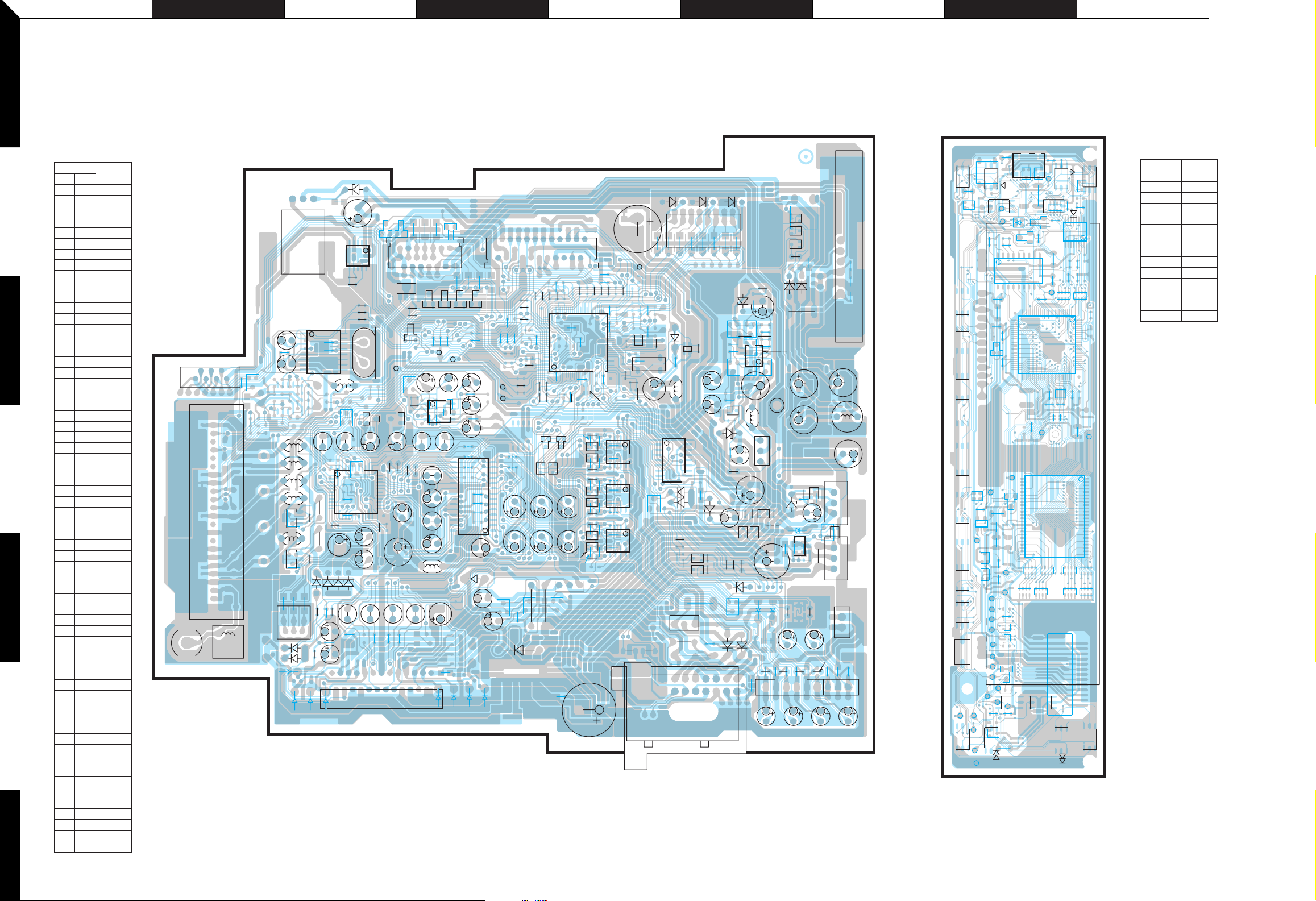
PC BOARD (Component Side View)
1
ELECTRIC UNIT
SWITCH UNIT
X13-9940-10 (J74-1134-02)
SWITCH UNIT
(X13-9940-10)
.ON.feR
CIQ
1Q3
2Q2
3Q2
4Q4
5Q4
6Q2
2Q2
3Q5
4R2
5Q5
6Q2
7Q2
8Q6
sserddA
S2
CP3
R29
S17
9
8
R34
R39
R21
R6
Q4
IC6
R27
100
26
C2
L10
CP15
B
R33
CP2
2
J1
14
1
25
S1
E
16
1
L8
C1
R11
CP20
CP16
EJECT
R26
L12
C14
R28
S.GND
1
24
S18
FM
E
B
S15
DISP
S6
S12S11
S13
S21
KR4
R18
S7
S8
S10S9
D2
C17
IC5
4
3
3.3V
Q3
E
Q5
SCREQ
P RESET
SC DATA
MC CLK
MC
REQ
KS2
KR5
KS1
AM
S.GND
R17
1
ED1
E
RST
R9
KR3
S22
C8
S5
KR1
KS3
R5
R4
R3
1
18
C12
C11
C5
C4
CLK
DO
C15
5
C16
1
L11
L9
R23
B
R22
B
DGND
18
FAC
FL GND
ANA
KR2
R8
E
Q8
B
S16
12
4
Q6
Q7
R19
BBEE
R20
ATT
S4
C19
3
IC3
KS4
R2
R1
D1
CP1
D4
R35
R36
D5
9
C10
IC2
C9
10
R24
76
75
51
50
R30
R31
VDD
48
D7
25
FAC
CP18 CP19
CP14
R12
R14
CP4
CP21
R40
DI
IC1
C3
L1
IC4
CP17
CP13
1
R25
D6
C18
D3
R13
FL+B
S20
15
S19
C6
dB
C7
R7
S3
X1
CP22
ELECTRIC UNIT
IC6
D3
C98
R10
C14
D2
C7
R180
A1
Q10
E
B
E
B
Q12
R11
C11
C10
C13
R2
C4
B
C5
R8
IC3
R6
6
E
B
R12
C17
C18
D6
1
C12
C15
L2
C3
Q2
B
R1
E
B
I
Q6
G
O
R5
Q4
E
E
B
E
Q5
B
Q1
E
CN2
R179
C103
1
C109
2
1
C113
C110
1
C104
R190
C108
C111
Q2
CLK 1 2 3 4 5 6
TI
S14
RST
CN1
C101C102C96C95
(X25-8730-10)
.ON.feR
CIQ
1N3
2L4
2
3O5
4L6
5M4
6O3
7N4
8M4
01N5
11N4
21N4
41L3
51L2
61O3
3
1P5
2O4
3N3
4P4
5P5
6P5
7O5
8O5
9L2
01O2
11O2
21O2
4
31O2
41N4
51O5
61O4
71O4
81O3
91O3
02O3
12O3
22O3
32O3
42O5
5
52O5
62N5
72M5
82M5
92N5
03O4
13O5
23M4
33N4
43L3
53L4
63L4
6
73N5
83N5
sserddA
CN7
1
F/E
C139
24
C137
C135
C133
C131
WH1
X25-8730-10 (J74-1142-02)
C142
C144
R242
C143
BE
7
Q52
R241
L13
L12
L11
L10
Q45
Q46
L9
Q43
1
L7
R156
CN4
D31
D30
D38
Q9
1
C141
8
E
B
E
B
E
BE
B
Q44
R155
R157
13
D40
D39
IC14
R213
R211
C115
C129
BE
C145
C146
C76
C74
R210
R201
L14
R98
R212
D32
R200
C147
C148
C77
44
1
R150
11
R202
25
D41
12
D29
24
R9
C9
C69
R203
R216
R215
R214
Q36
EB
C75
C73
C72
D28
R204
C116
5
6
16
9
R151
C70
C150
D4
IC15
BE
R152
D27
R158
IC2
C68
C67
10
D26
C66
Q35
C71
C117
1
X3
34
22
R207
C149
33
R205
IC4
D25
23
R153
D49
13
R231
R230
NOISE
R145
R146
C65
C88
C63
R154
C61
R208
Q51
B
Q34
D50
12
EB
C84
C62
R206
E
R144
C87
C118C119 C120
C79
C81
R239
CN6
D48
SMTR
C49
R140
R147
C83
C82
C85
1
4
C86
R237
L6
2
R81
IC8
1
R235
C54
R148
C114
R79
C50
R143
C78
TH1
D36
2
1
R83
28
R141
D21
5
15
D47
R236
D15
R234
R89
R90
R95
IFC-OUT
C51
8
W4
W3
IC5
C60
C36
D35
CN5
222
121
R233
C92
C34
D44D46 D45
C91
C89
C90
R232
R84
R86
R88
C46
R91
R93
R99
R92
R100
R108
R94
R109
R102
R142
C52
C55
C53
W2
W1
R110
CLK
R113
R114
DATA
W6
14
W5
C99
1
Q28
Q27
EB
E
C35
R40
R82
R115
E
Q32
C105
C94C93
B
R80
76
100
R116
D20
R101
B
R38
R39
R223
R85
R97
R117
R118
E
R224
75
1
R104
B
C106
BE
R77
C100
B
R225
R78
IC1
R119
R120
Q41
Q33
L5
Q39
Q40
Q37
R121
D19
Q42
R175
R166
Q38
Q29
R125
R122
R185
R171
R176
R165
E
R75
R186
B
B
E
B
E
B
E
R172
B
B
E
R74
R107
R124
R182
Q26
R72
R73
R50
E
R181
R162
E
R161
W7
D1
C1
C2
D33
D34
51
R71
R126
25
TEST
4
R184
R188
R183
5
4
R173
R177
R178
R174
5
4
R164
R168
R167
R163
5
R220
50
26
W9
R221
R70
R62
R61
C41
R127
W8
L1
R69
R187
W10
D23
C200
D24
8
D22
CN3
Q11
B
E
1
Q13
RST
R66
R60
R59
X1
R49
C43
C42
R4
R3
E
B
Q3
1
IC12
8
1
IC11
8
1
IC10
8
R56
R55
R54
R53
C40
EB
R52
R51
C44
X2
1
7
R132
D7
R17
R20
R48
D18
IC16
IC7
Q14
R131
R67
D8
R133
2
3
C48
C39
8
Q15
Q31
1
4
L4
C32
14
R135
C37
R41
D16
B
E
B
R134
C45
C33
C22
E
D9
Q19
R23
C21
R47
R130
R30
R31
R21
R32
C31
C20
R137
C28
Q22
R22
B
C27
Q20
BE
Q8
R136
R24
D5
D10
R25
Q18
E
B
B
5
8
B
Q21
Q17
B
E
C23
R42
B
E
R16
R14
C29
R26
E
C26
R28
C25
R27
E
C30
4
R29
E
E
B
1
Q23
C24
E1
L3
B
Q16
E
C6
Q30
B
R43
R44
E
B
E
W100
C8
Q7
R7
D17
R34
BE
Q24
D11
D13
R13
R189
C107
R37
R33
C112
C97
6
R170
9
R19
R15
Q25
B
E
W15
D14
R46
R36
R45
C38
1
16
D12
R169
8
9
J1
93N4
04N4
14N4
24N4
34L5
44L5
54L4
64L4
15L3
7
25K3
9
Refer to the schematic diagram for the values of resistors and capacitors.
10
 Loading...