


Kenwood KD-CX-8009-U, KD-CW-7541-UY, KD-CW-7541-U, KD-CMP-738-U, KD-CX-792 Service Manual
CD RECEIVER
KDC-MP738U/W7541U
/W7541UY/X792/X8009U
SERVICE MANUAL
© 2008-3 PRINTED IN JA PAN
B53-0628-00 (N) 429
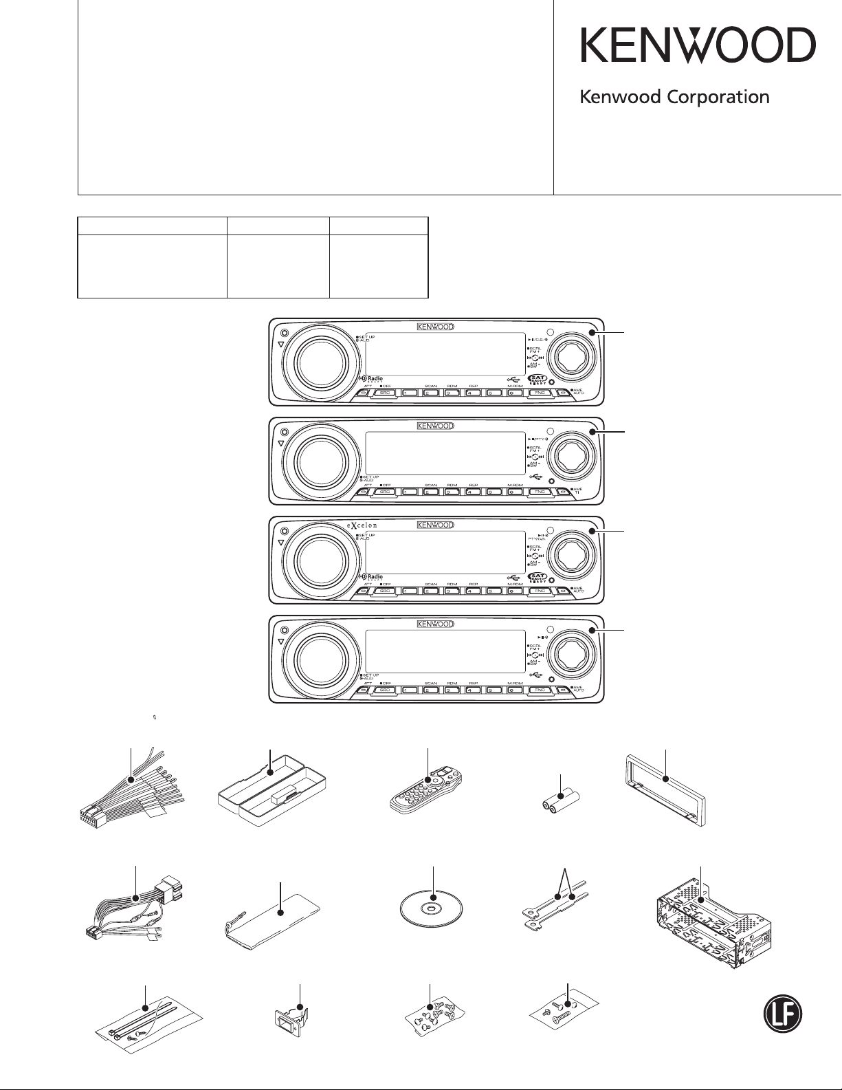
TDF SPARE-PANEL
MODEL TDF PANEL No. TDF NAME
KDC-X792 Y33-2940-60 TDF-88DX
KDC-MP738U Y33-2940-61 TDF-MP88D
KDC-W7541U/W7541UY Y33-2940-64 TDF-W7541U
KDC-X8009U Y33-2940-66 TDF-X8009U
CD MECHANISM EXTENSIONCORD (30P) : E39-1014-05
KDC-MP738U
(K type)
KDC-W7541U
KDC-W7541UY
(E type)
KDC-X792
(K type)
KDC-MP738U
KDC-W7541U
KDC-X792
Panel assy
(A64-4425-02)
Panel assy
(A64-4428-02)
Panel assy
(A64-4424-02)
KDC-X8009U
(M type)
DC cord (K,M type)
(E30-6428-05)
DC cord (E type)
(E30-6671-05)
Screw set (KDC-X792)
(N99-1790-05)
Plastic cabinet assy (M type)
(A02-2757-03)
Carrying case
(W01-1664-05): KDC-X792
(W01-1710-05): K,E type
Cover (KDC-X792)
(F19-1475-04)
Remote controller assy
(A70-2085-05)
RC-547
Compact disc
(W01-1723-05)
Screw set (K,M type)
(N99-1757-15)
KDC-X8009U
SIZE AA BATTERY
(Not supplied)
Lever
(D10-7012-04) x2
Screw set (K,M type)
(N99-1730-35)
Panel assy
(A64-4431-02)
Escutcheon
(B07-3238-03): KDC-MP738U
(B07-3235-03): K,E,M type
Mounting hardware assy
(J22-0011-03)
This product complies with the
This product uses Lead Free solder.
RoHS directive for the European market.
KDC-MP738U/W7541U
/W7541UY/X792/X8009U
(X34-579)
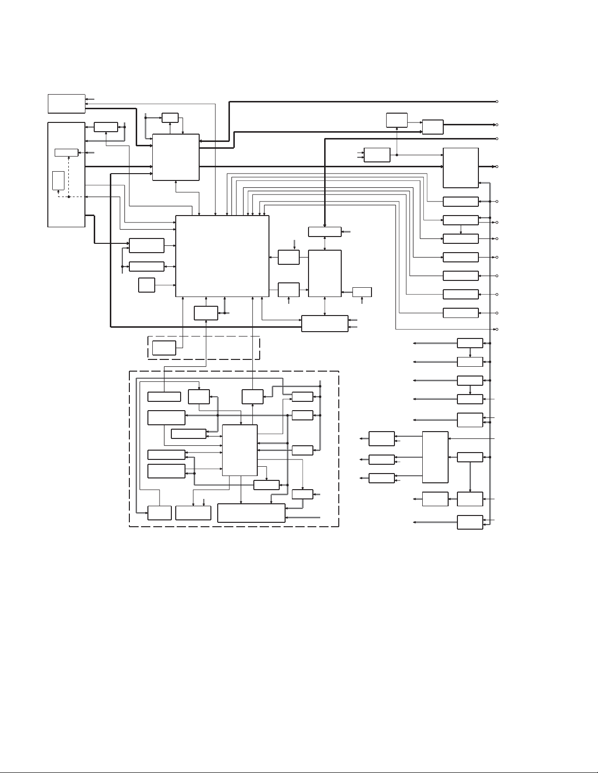
LX BUS
(FST)
E2PROM
FST
F/E
BACK UP
Q400
AM+B
SW5V
PANEL
(X16- )
A8V
IC340
RDS
DECODER
ROM CORR
SW5V
SUB PANEL
(X15-119)
A8V
IC480
FLIP
DET
RESET SW
KEY MATRIX
IC1
FLASH ROM
ROTARY
ENCODER
REMO.
CON.
AGC
CH
FM/AM
CD/USB
EJECT
SW
KEY
IC6
AUX
SAIN
SAOUT
E-VOL
IC500
IC510
RESET
IC
LEVEL LEVEL
SHIFT
ROM CORR
ILL+B
KEY ILL
BLOCK DIAGRAM
BU5V
SYSTEM
u-COM
IC4
ED1
BU5V
PANEL
u-COM
IC600
IC602
IC8IC7
SHIFT
SW 3.3V
FL
LEVEL
SHIFT
LEVEL
SHIFT
D3.3V
IC700
PAN5V
SW 5V
IC11
D 3.3V
IC10
D 2.5V
Q13
FL+B
USB
SOC
CD
FL+B
FDC
RST
BU5V
VBUS
FDC
PAN5V
BVUS
IC20
D3.3V
BU5V
BU5V
SERVO+B
IC530
MUTE
DRIVER
IC300
HISIDE
SW
Q45
Q40
PAN5V
FDC
Q371,377
SW
MUTE
SW14
BU5V
SW5V
SERVO+B
FL+B
ILL+B
A8V
SW VBU
PON ILL
PON PA
Q370,372-376
PRE
MUTE
IC80
USB 5V
FDC
PAN5V
IC60
DC/DC
(FL)
IC450
POWER
IC
Q120
B.U DET
Q143
P-CON
Q150
ANT-CON
EXT AMP
Q180
DIMMER
TEL MUTE
Q122
ACC DET
Q13
Q10
Q20
Q22
Q30
Q70
Q70
Q50
SW 14V
A8V
BU5V
SW 5V
SERVO
+B
SW 20V
SW
FL+B
ILL+B
AUX IN
PRE OUT
(F/R SW)
USB
SP OUT
(FL/FR/RL/RR)
BACK UP
P CON
ANT CON
EXT.AMP.CON
DIMMER
LINE MUTE
ACC
WIRED REMO
OPEL DISP
PON
SW14
PON D5
PON ILL
PON ILL
2
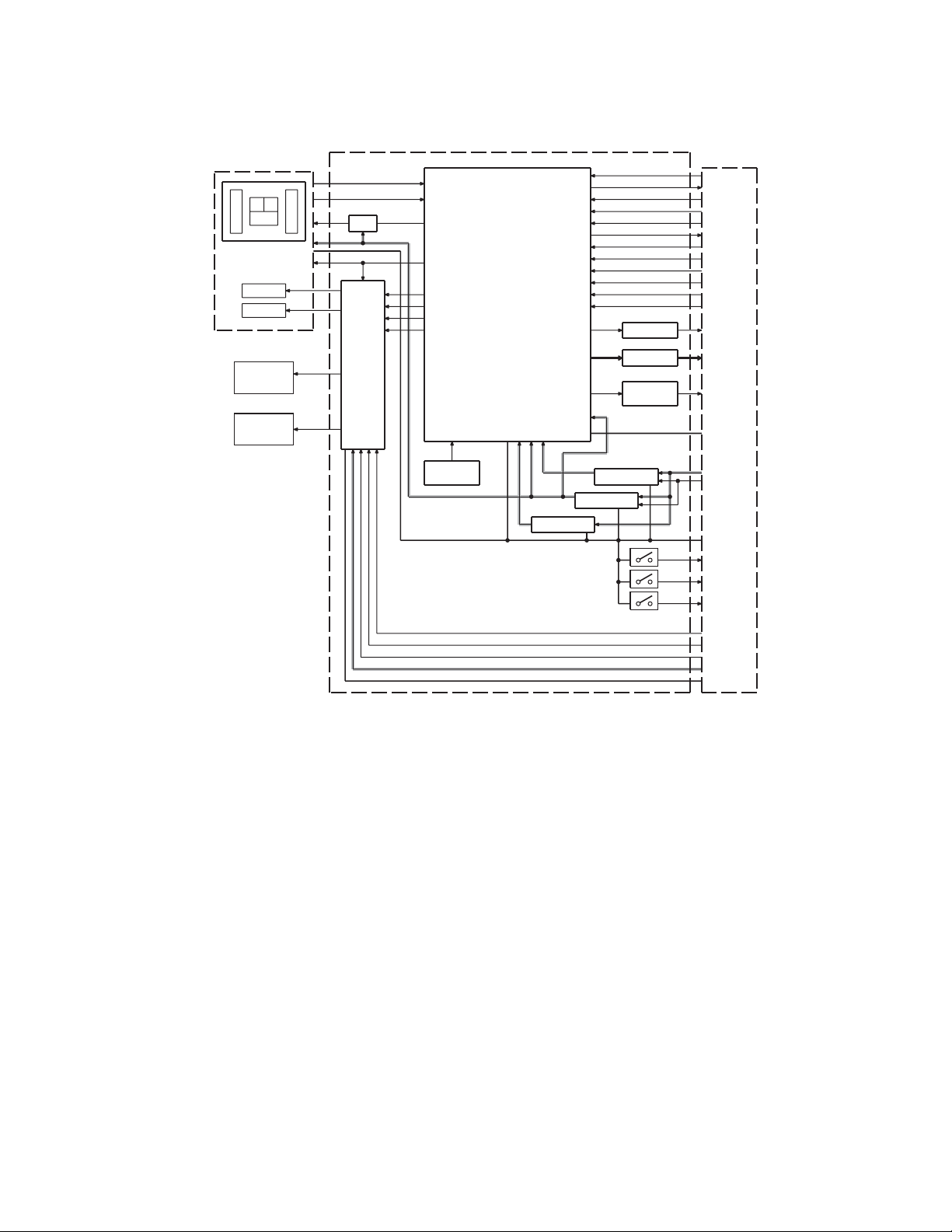
BLOCK DIAGRAM
KDC-MP738U/W7541U
/W7541UY/X792/X8009U
DPU1
ACB
EF
FO COIL
TR COIL
DM1
LOADING &
SPINDLE
MOTOR
DM2
LOADING &
SLED
MOTOR
CD PLAYER UNIT (X32-6130-00)
IC4
SIGNAL
A,B,C,E,F
Q1
APC
IC3
FO OUT
TR OUT
MOTOR
DRIVER
DM OUT
FM OUT
PD
LD
VREF
FO OUT
TR OUT
DM OUT
FM OUT
X1
CLOCK
16.934MHz
RF AMP
SERVO
PROCESSOR
MP3 DECODER
WMA DECODER
AAC DECODER
1M bit SRAM
MOTHER
BOARD
(X34- )
SRAMSTB
SO
SI
BUCK
CCE
PIO0
+
+
+
+
+
MRST MRST
BSIF ST REQ
BSIF GATE
BSIF DATA
BSIF BCK
BSIF LRCK
R-ch
L-ch L-ch
C88,R82
CR FILTER
C87,R83
CR FILTER
SRAMSTB
SO
SI
BUCK
CCE
PIO0
BSIF ST REQ
BSIF GATE
BSIF DATA
BSIF BCK
BSIF LRCK
R-ch
Q13
REVERSAL
CIRCUIT
IC5
SW1.5V REG
A8V
A.GND
BU5V
P.ON
D GND
BU1.5V
ZDET MUTE L/R
A3.3V
AGND
SW1.5V
SW3.3V
IC6
IC11
SW3.3V REG
BU1.5V REG
D.GND
S1
LOS-SW
S2
12EJE-SW
S3
LOE-SW
8EJE-SW
DRV MUTE
LO/EJ
MOTOR
S7.5V
S.GND
3

KDC-MP738U/W7541U
/W7541UY/X792/X8009U
COMPONENTS DESCRIPTION
ELECTRIC UNIT (X34-579x-xx)
●
Ref. No. Application / Function Operation / Condition / Compatibility
IC10 Audio8V Ref Power Supply Output 1.27V.
IC20 Regulator Power supply for BU3.3V.
IC60 Switching Regulator Power supply for 65V FL+B. (to PANEL)
IC80 Switching Regulator Power supply for D5V. (to USB/PANEL)
IC300 Hi-side SW Detection of USB Over Current & On/Off SW
IC310 G-Sensor Inclination detection (only 0-10)
IC340 RDS decoder IC RDBS & RDS ecoder. (only K & E type)
IC350 OPAMP Vref of IC480
IC450 Power IC Amplifi es the front L/R and the rear L/R to 50W maximum.
IC480 Eelectrical Volume & Source Selecter Controls the source, volume, and tone.
IC500 System μ-com Controls FM/AM tuner, the changer, CD mechanism, Panel, volume and tone.
IC510 Reset IC “L” when detection voltage goes below 3.6V or less.
IC520 EEPROM Rom correction
IC530 Muting logic IC Controls logic for muting.
IC600 Logic IC Level Shift (3.3V→5V)
IC602 Logic IC Level Shift (5V→3.3V)
IC700 Sub μ-com USB/CD mechanism control
IC751 EEPROM Rom correction
IC752 iPod Authentication Coprocessor iPod Authentication
Q10 Audio8V AVR When Q11&Q12’ go ON, A8V AVR outputs 8.0V.
Q11,12 Audio8V AVR SW When Q12’ Base goes Hi, Supply current to IC10.
Q13,14 Audio8V AVR SW When Q14’ Base goes Hi, Q13 are ON.
Q20,21 B.U.5V AVR While BU is applied, BU5V AVR outputs +5V.
Q22,23 PON5V When Q23’ base goes Hi, PON5V outputs +5V.
Q30 Servo +B SW When Q31’ go ON, Servo +B outputs 8V.
Q31 Servo +B SW When Q13’ go ON, Q30 are ON
Q40,41 PANEL +5V SW When Q41’ base gose Hi, PANEL +5V is outputs.
Q45,46 FDC SW When PON-ILL (μ-CON) goes ON, AVR outputs 5V. (FL Filament)
Q50,51 Illumination+B AVR When Q52&Q53’ go ON, AVR outputs 10V.
Q52,53 Illumination+B SW When PON-ILL (μ-CON) goes ON, Hi, Q52 is ON.
Q70,71 SW15V When Q13’ go ON, The voltage appears. (~15V)
Q80 Change of Oscillation Frequency
Q120 B.U Detected SW When Q120’ base gose Hi, B.U voltage is detected.
Q122 ACC Detect SW When Q122’ base gose Hi, Acc voltage is detected.
Q123 Surge Detect SW When Q123’ base goes Hi, Surge voltage is detected.
Q140,143 P-CON SW When Q140’ base goes Hi, AVR outputs 14V.
Q141,142 P-CON Protect Protect Q142 by turning on when P-CON output is grounded
Q150,151 Power Antenna SW When Q151’ base goes Hi, power antenna switch outputs 14V.
Q180 Small-lamp Detect SW When Q180’ base goes Hi, Small-lamp is detected.
When Q80 is turned ON, the oscillation frequency at IC80 in the switching regulator
changes from 1MHz to 2.45MHz.
4
KDC-MP738U/W7541U
/W7541UY/X792/X8009U
COMPONENTS DESCRIPTION
Ref. No. Application / Function Operation / Condition / Compatibility
Q350,351 4VPRE+B When Q353’ go ON, 4VPRE+B is outputs. (~12V)
Q352 4VPRE+B Protect When 4VPRE+B is overcurrent, Q352 turn Q350 off.
Q353,354 4VPRE+B SW When Q354’ Base goes Hi, Q353 is ON.
Q370,372~376 Pre-out mute SW When a base gose Hi, Pre-out is set to mute.
Q371,377 Pre-out mute driver When a base gose Lo, mute driver is turned on.
Q400,401 AM+B SW When Q401’ base gose Hi, AM+B is outputs.
Q500,501 FL+B SW When PON-ILL (μ-CON) goes ON, FL+B outputs 65V.
Q650 X15 LED SW When DSI Port LOW, LED of X15 are ON
Q702,703 3.3V_SW_for_IC700 (fl ash_type) When base of Q702 is “H”, 3.3V_On.
Q704
Q705 CD “LOE_LIM” SW_Buffer When base of Q705 is “H”, Loading_End.
Decoder SRAM standby control
Buffer
When base of Q704 is “L”, SRAM_STBY.
SWITCH UNIT (X16-624x-xx)
●
Ref. No. Application / Function Operation / Condition / Compatibility
IC1
IC3 ROM CORRECTION For program correcting emergency (EEP_ROM)
IC4 PANEL μ-COM FL VddSupply (ON/OFF) Encoder Key LedSW (ON/OFF) is controlled by IC4
IC6 REMOTE CONTROL IC Remote control receiver
IC7 BUFFER IC It is change into 3.3V from 5V
IC8 BUFFER IC It is change into 5V from 3.3V
IC9 BUFFER IC For Control ED1
IC10 2.5V REGULATOR The power supply for 2.5V
IC11 3.3V REGULATOR The power supply for 3.3V
Q1~5 LED DRIVER It is controlled by IC4
Q6 POWER ON/OFF SWITCH OF IC1 It is controlled by IC4
Q11,13
CD PLAYER UNIT (X32-6130-00)
●
Ref. No. Application / Function Operation / Condition / Compatibility
IC3 4ch BTL Driver
IC4 Servo DSP with built-in Audio DAC With built-in MP3/WMA/AAC decoder and 1M-bit-SRAM.
IC5 D1.5V REG. Power supply for digital 1.5V.
IC6 D3.3V REG. Power supply for digital 3.3V.
IC11 BU1.5V REG. Power supply for back-up 1.5V.
Q1 APC (Auto Power Control) Drives LD (Laser Diode).
Q13 Inverter Inverts ZDET signal.
D2 Laser Diode Protection Prevents reverse bias which is applied to laser. Laser destruction prevention.
D3,4 Static Electricity Countermeasure Prevents malfunction by static electricity.
ROM IC
FLASH ROM IC
POWER ON/OFF SWITCH OF ED1
(65V)
Graphics data included
It is controlled by IC4
Driver for focusing & tracking coil, driver for sled & spindle motor, and operation for
disc loading & ejection.
5
KDC-MP738U/W7541U
/W7541UY/X792/X8009U
MICROCOMPUTER’S TERMINAL DESCRIPTION
SYSTEM MICROCOMPUTER 30624MGPB77GP (X34: IC500)
●
Pin No. Pin Name I/O Application
1 WIRED_REMO I Remote controller input Pulse width detection
2 RDS_QUAL I RDS decoder QUAL input terminal
2 NC O Not used. (In models without RDS) Output L fi xed
3 S_SYS_DATA O System μ-com → SOC data 400k
4 S_SOC_DATA I SOC → System μ-com data 400k
5 S_SOC_CLK I Host is SOC. CLK from SOC 400k
6 BYTE
7 CNVSS
8 XCIN 32,768Hz
9 XCOUT 32,768Hz
10 RESET
11 XOUT 12MHz
12 VSS
13 XIN 12MHz
14 VCC1
15 NMI I Not used
16 RDS_CLK I RDS clock input terminal
16 NC O Not used. (In models without RDS) Output L fi xed
17 FLIP_DET I FLIP panel open detection
18 SRC_KEY I Source key input H: OFF, L: ON
19 RDS_DATA I RDS decoder DATA input terminal
19 NC O Not used. (In models without RDS) Output L fi xed
20 PANEL_SW_DET I FLIP panel detach detection
21 EJECT_KEY I Eject key input H: OFF, L: ON
22 PANRST O Panel reset terminal H: Normal, L: Reset
23 DSI (EJECT_ILL) I/O DSI control terminal L: Turns on, Hi-Z: Turns off
24 NC O Not used (SW_REG frequency setup terminal 2) Output L fi xed
25 F_SEL1 I/O SW_REG frequency setup terminal 1
26 PWIC_BEEP O Beep output 2kHz 1kHz
27 TUN_SCL I/O F/E I2C clock input/output terminal MAX 400k
28 TUN_SDA I/O F/E I2C data input/output terminal MAX 400k
29 PAN_SYS_DATA O System μ-com → Panel data UART MAX500k
30 PAN_PAN_DATA I Panel → System μ-com data UART MAX500k
31 PAN_SYS_REQ O System μ-com → Panel communication request
32 PAN_PAN_REQ I Panel → System μ-com communication request
33,34 NC O Not used Output L fi xed
Truth
Value Table
t
Processing / Operation / Description
H: Open, L: Close
Shut down power to panel system in synchronous
with opening the panel. Audio shall be kept on
H: Panel attached, L: Panel detached
Enter PowOFF condition simultaneously with
detection
H: For AM, Hi-Z: For other than AM
6
KDC-MP738U/W7541U
/W7541UY/X792/X8009U
MICROCOMPUTER’S TERMINAL DESCRIPTION
Pin No. Pin Name I/O Application
35 NC (D5V_DIS) O Not used Output L fi xed
Panel LED
36 PON_ILL I/O
37 NC O Not used Output L fi xed
38 PON_PANEL I/O
39 ROMCOR_DET I ROM correction writing-in request
39 EPM I
40 CD_MOTOR O CD motor control terminal
41 CD_LOE_LIM_SW I CD detection terminal (Chucking detection) H: Loading completed, L: No disc is found.
42 CD_LOS_SW I CD loading detection terminal L: Ejection completed.
43 CD_DISC12_SW I CD disc detection terminal (12cm) L: 12cm disc
44 PAN_SC_CON O
45 CD_LOEJ I/O CD motor control terminal
46 S_SOC_REQ I SOC → System μ-com communication request
47 SOC_STOP O SOC stop terminal H: Normal, L: Stop SOC.
48 SOC_RST O SOC reset terminal H: Normal, L: Reset
49 S_SYS_REQ O System μ-com → SOC communication request
50 SOC_MUTE I SOC mute request L: MUTE request, H: In normal condition
51 PON_D5V I/O
52 PON I/O Power supply control terminal H: ON, Hi-Z: OFF
53 OEM_DISP_DATA I/O External display DATA External display
53 NC O Not used (Model without OEM_DISP) Output L fi xed
54 OEM_DISP_CLK I/O External display CLK External display
54 NC O Not used (Model without OEM_DISP) Output L fi xed
55 OEM_DISP_CE I/O External display control request External display
55 NC O Not used (Model without OEM_DISP) Output L fi xed
56 P_CON I/O PCON control terminal
57 ANT_CON O ANTCON control terminal
58 NC O Not used Output L fi xed
59 ILLUMI_DET I Dimmer illumi detection L: ON, H: OFF
60 VCC2
61 MUTE_0 O IC-2 FRONT MUTE control
62 VSS
63 MUTE_1 O IC-2 REAR MUTE control
FL fi lament power supply
FL bias power supply control
Power supply for panel μ-com
Required for panel authentication
EPM input terminal for re-writing ROM. ROM is
re-writable when the input is “L” at the boot up.
Panel operation control terminal
CE when the system μ-com is re-written
5V power supply control terminal for FL fi lament,
panel, and USB.
Truth
Value Table
w
w
Processing / Operation / Description
H: ON, Hi-Z: OFF
Turned OFF when the display is black out.
Turned OFF when panel is dismounted/opened.
H: ON, Hi-Z: OFF
Turn OFF when panel is dismounted/opened or
when power is off.
H: Can re-write ROM (ROM correction)(I2C is open)
Refer to the truth value table
H: In normal condition, L: Stop the panel.
Refer to the truth value table
H: ON, Hi-Z: OFF
POWER ON: H, POWER OFF: Hi-Z
STBY source: Hi-Z
TUNER source: H, POWER OFF: L
STBY source: L
L: Mute ON, Independent setup of time
constant 10ms, H: In normal condition
L: Mute ON, Independent setup of time
constant 10ms, H: In normal condition
7
KDC-MP738U/W7541U
/W7541UY/X792/X8009U
MICROCOMPUTER’S TERMINAL DESCRIPTION
Pin No. Pin Name I/O Application
64 MUTE_2 O IC-2 SW MUTE control
65 LINE_MUTE I Line mute detection
66 NC (SA_IN) O Not used Output L fi xed
67 NC (SA_RST) O Not used Output L fi xed
68 NC (SA_CLK) O Not used Output L fi xed
69 NC (MUTE_SA) O Not used Output L fi xed
70 PWIC_DC_DET I DC offset detection terminal
71 ACC_DET I ACC detection L: ACC found, H: ACC not found
72 BU_DET I BU detection
73 LX_REQ_S I Communication request from slave unit
74 MUTE_AFS I/O
74 NC I Not used (For other type than E-TYPE) Input Hi-Z fi xed
75 SDA/EVOL_SDA I/O System μ-com → IC-2 data output Communication speed 200-400k
75 SDA/E2P_SDA I/O I2C data for ROM correction Communication speed 200-400k
76 SCL/EVOL_SCL I/O System μ-com → IC-2 CLK output Communication speed 200-400k
76 SCL/E2P_SCL I/O I2C clock for ROM correction Communication speed 200-400k
77 PWIC_MUTE O Power IC MUTE terminal
78 PWIC_STBY O Power IC standby terminal POWER ON: H, POWER OFF: L
79 LX_REQ_M O Communication request to slave unit
80 LX_MUTE I MUTE request from slave unit H: Mute ON, L: Mute OFF
81 LX_CON O Start-up request to slave unit H: Slave unit ON, L: Slave unit OFF
82 LX_RST O Hardware-reset to slave unit H: RST, L: Normal
83 MUTE_PRE_FR O External PREOUT_MUTE F/R “L” when Obit, or momentary power down
84 MUTE_PRE_SW O
85 PON_AM I/O AM+B power supply control terminal
86 TUN_IFC_OUT I F/E IFC OUT input terminal H: Station is found., L: No station is found.
87 TUN_SMETER I S meter voltage detection terminal
88 RDS_NOISE I FM noise voltage detection terminal
88 NC O Not used. (In models without RDS) Output L fi xed
89 RDS_AFS_M I/O Time constant switching when noise is detected
89 NC O Not used. (In models without RDS) Output L fi xed
90 TYPE_1 I A/D 5 pattern
91 TYPE_2 I A/D 5 pattern
92 G_Y_OUT I Detection of Y direction movement of G analyzer
92 NC O Not used. (In models without G antenna) Output L fi xed
IC-2 MUTE_C control
AFS MUTE
External PREOUT_MUTE SUB
MUTE_2 shock noise measure
Truth
Value Table
e
q
q
Processing / Operation / Description
L: Mute ON, Independent setup of time
constant 10ms, H: In normal condition
Shall be used together with MUTE_PRE_SW
IC2 shock noise measure
TEL MUTE: 1V or less, NAVI MUTE: 2.5V or higher
L: BU found, H: When No BU
Reduction of power, and Over voltage
L: Mute ON, Independent setup of time
constant 0.5ms, Hi-Z: While in normal
L: While STANDBY source, momentary power
down, L: While TEL MUTE
“L” when Obit, or momentary power down
Shall be used in addition to MUTE_2.
H: ON when AM is being received.
Hi-z: OFF in other condition.
L: During AF search, Hi-Z: In normal condition
8
KDC-MP738U/W7541U
/W7541UY/X792/X8009U
MICROCOMPUTER’S TERMINAL DESCRIPTION
(90)
(91)
Truth
Value Table
r
Processing / Operation / Description
R540 R530 R529 R528
1 - - x 22K
2 - - 47k 22k
3 - - 22k 22k
4 - - 22k 47k
5 - - 22K x
1 x 22K - -
2 47k 22k - -
3 22k 22k - -
4 22k 47k - -
5 22K x - -
Pin No. Pin Name I/O Application
93 G_X_OUT I Detection of X direction movement of G analyzer
93 NC O Not used. (In models without G antenna) Output L fi xed
94 AVSS
95 NC O Not used Output L fi xed
96 VREF A/D analog reference voltage
97 AVCC
98 LX_DATA_S I Data from slave unit
99 LX_DATA_M O Data to slave unit
100 LX_CLK I/O LX BUS clock
Destination setting
q
TYPE_2 (91) TYPE_1 (90) Destination
1 1 KDC-MP738U [∗]
1 2 KDC-X792
1 3 KDC-X692
1 4 SKDCMP9090U(Visteon)
1 5 KDC-MP638U
2 1 KDC-X8009U
22
23
24
2 5 KDC-X7009U
3 1 U737 (J)
32
3 3 (Reserve)
34
35
4 1 KDC-W7541UY
42
43
44
4 5 KDC-W7141UY
5 1 KDC-W7541U
52
53
54
5 5 KDC-W7041U
(Note 1) When there is no destination defi ned, the unit operates as
the model for [∗].
(Note 2) The voltage is set to higher value.
(Note 3) When the system is set up as “Reserve”, it reads the data
for setting up the destination from E2PROM. Set up for the
destination. In addition, change of the destination shall be
possible from MENU in the test mode.
TYPE1
TYPE2
9
KDC-MP738U/W7541U
/W7541UY/X792/X8009U
MICROCOMPUTER’S TERMINAL DESCRIPTION
CD_MOTOR, CD_LOEJ
w
CD_MOTOR CD_LOEJ
Standby L L
Eject H H
Load H L
Brake H Hi-z
AFS process
e
RDS_AFS_M Status
AFS LOW L No sound output AF search
AFS MID L There is sound output in AF search.
AFS HIGH Hi-Z Normal reception
CH_CLK
r
AM10k AM9k
122.4 116.5 111.1 106.2 101.7 122.4 116.5 111.1 106.2 101.7
530 1170-1180 860-930 1050-1060 540-660 522-558 864-990 1071-1116 1260-1314 567-657
670-780 1390-1410 1070-1160 790-850 666-801 1125-1215 1323-1350 1449-1512 810-855
940-1040 1280-1380 1590-1680 1224-1251 1359-1413 1521-1629 999-1062
1190-1270 1530-1580 1422-1440
1420-1520
1690-1700
• Other than AM: 122 [kHz]
F_SEL
t
ALL-Type
FSEL1 Receiving frequency
Hi-Z Other than AM
H For AM
10
KDC-MP738U/W7541U
/W7541UY/X792/X8009U
MICROCOMPUTER’S TERMINAL DESCRIPTION
SUB MICROCOMPUTER 92CD28AFG6VV1 (X34: IC700)
●
Pin No. Pin Name I/O Application Processing / Operation / Description
1 MRST - Reset L: RESET, H: In normal condition
2 MSTOP I
3 REQ_S I REQ signal from system μ-com L: Request
4 IPOD_RDY I RDY signal of iPOD authentication
5 BSIF_ST_REQ I BSIF
6 VCC - Power supply terminal (For PC port and PMC circuit)
7 XT1 -
8 XT2 -
9 PWE - External power supply control output L: STOP
10 DVSS - GND terminal
11 DVCC1B - For power supply terminal and built-in SRAM
12 RVOUT1 -
13 RVIN -
14 RVIN -
15 RVOUT2 -
16 DVCC1A - For power supply terminal and built-in logic
17 DVSS - GND terminal
18~22 NC O Not used Output L fi xed
23 CD_CCE O Command I/F, CD mechanism chip enable terminal “L” during other source
24 CD_RST O RESET, CD mechanism RST terminal H: Normal, L: Reset
25 NC O Not used Output L fi xed
26 DVSS - GND terminal
27 DVCC3A - For power supply terminal and peripheral I/O
28 CD_REQ I
29 CD_SRAMSTBY O Decoder SRAM STANDBY control L: SRAM standby (6E∗∗)
30 CD_DRIVEMUTE O CD motor drive mute output
31 CD_PON O CD mechanism power supply control output H: Power ON (6E∗∗), Hi-z: Power OFF
32~43 NC O Not used Output L fi xed
44 DVSS - GND terminal
45 DVCC3A - For power supply terminal and peripheral I/O
46~61 NC O Not used Output L fi xed
62 DVSS - GND terminal
63 DVCC3A - For power supply terminal and peripheral I/O
64 NC O Not used Output L fi xed
65 ZDET_IN I ZDET, 0 bit mute request terminal L: Mute request, H: While in normal
STOP signal from system μ-com(Momentary power down
detection / Recovery to low power consumption mode)
Low frequency oscillator connection terminal
sub-clock 32.768kHz
Low frequency oscillator connection terminal
sub-clock 32.768kHz
Built-in regulator 1.5V output
(Flash version does not output voltage).
Built-in regulator power supply input
(Flash version has power supply terminal).
Built-in regulator power supply input
(Flash version has power supply terminal).
Built-in regulator 1.5V output
(Flash version does not output voltage).
Command I/F
Communication request terminal from mechanism DSP
H: Normal
L: Stop SOC
H: Data request
11
KDC-MP738U/W7541U
/W7541UY/X792/X8009U
MICROCOMPUTER’S TERMINAL DESCRIPTION
Pin No. Pin Name I/O Application Processing / Operation / Description
66 CD_MUTE O Mute request to system μ-com L: Mute request, H: While in normal
67 REQ_M O REQ signal to system μ-com L: Request
68 IPOD_RST O RESET
69 BOOT I Terminal for writing FLASH
69,70 NC O Not used Output L fi xed
71 BSIF_LRCK - BSIF
72 AM1 - Operation mode: Fixed to “1”.
73 X2 -
74 DVSS - GND terminal
75 X1 -
76 DVCC3A - For power supply terminal and peripheral I/O
77 USB_OC I USB over current detection L: Detection, H: In normal condition
78 USB_PON O USB PON output
79 USB_D+ - USB data connection terminal
80 USB_D- - USB data connection terminal
81 AM0 - Operation mode: Fixed to “1”.
82 CD_LOE_LIM_SW I CD detection terminal (Chucking SW) L: Loading completed, H: No disc
83 DVSS - GND terminal
84 DATA_M O Serial I/F with system μ-com (Sending)
85 DATA_S I Serial I/F with system μ-com (Recieving)
86 CLK O Serial I/F with system μ-com (Clock output) f=1M or less
87 CD_SO O Command I/F, Serial I/F (Sending) “L” during other source
87 FLSH_UO O Terminal for writing FLASH
88 CD_SI I Command I/F, Serial I/F (Receiving)
88 FLSH_UI I Terminal for writing FLASH
89 CD_CLK O Command I/F, Serial I/F (Clock output) f=1MHz, “L” during other source
90 ROMCOR_SDA I/O E2PROM I2C data I/O terminal for ROM correction
90 IPOD_SDA I/O I2C iPOD authentication data I/O terminal
91 ROMCOR_SCLK I/O E2PROM I2C clock output terminal for ROM correction
91 IPOD_SCLK I/O I2C iPOD authentication clock output terminal f=80kHz
92 BSIF_BCK - BSIF “L” during other source
93 BSIF_DATA - BSIF “L” during other source
94 BSIF_GATE O BSIF
95 DVCC3A - For power supply terminal and peripheral I/O
96 NC I Not used
96 ROMCOR_DET I ROMCOR write detection H: Writing-in
97~99 NC I Not used
100 DVSS - GND terminal
High frequency oscillator connection terminal
Main clock 9.00MHz
High frequency oscillator connection terminal
Main clock 9.00MHz
12
KDC-MP738U/W7541U
/W7541UY/X792/X8009U
MICROCOMPUTER’S TERMINAL DESCRIPTION
PANEL MICROCOMPUTER 703134AGJ018A (X16-624: IC4)
●
Pin No. Pin Name I/O Application Processing / Operation / Description
1~7 D14-D8 I/O Data input/output
8 3.3VDD - 3.3V
9 VSS -
10~17 D7-D0 I/O Data input/output
Control lighting time (brightness tone) with the
18 FLGCP1 O FL tone control
19 NC O Output L fi xed
20 SYS_REQ I System μ-com communication request input H: During data communication
21 SC_CON I
22 NC O Output L fi xed
23 2.5VDD - 2.5V
24 VSS -
25 PWM_VOL O PWM output H: ON, L: OFF
26 PWM_MULTI O PWM output H: ON, L: OFF
27 KS1 I/O Key scan output Output L, Hi-Z: Switching
28 TDO O Be used during debugging NC during normal operation
29 TDI O Be used during debugging NC during normal operation
30 FL_BK O FL BK control L: FL goes on, H: FL goes off
31 KS2 I/O Key scan output Output L, Hi-Z: Switching
32 TRST I Be used during debugging H or L during debugging
33,34 KS3,KS4 I/O Key scan output Output L, Hi-Z: Switching
35 TMS O Be used during debugging NC during normal operation
36 TCM O Be used during debugging NC during normal operation
37 3.3VDD -
38 EVSS -
39 KS5 I/O Key scan output Output L, Hi-Z: Switching
40~42 KR1-KR3 I Key return input
43 FLGCP2 O FL tone control
44 PAN_REQ O Panel communication request output H: During data communication
45 SYS_DATA I Data reception from system μ-com UART communication 500kbps
46 PAN_DATA O Data transmission from the panel UART communication 500kbps
47 FL CLK O FL serial communication reference clock Reference clock 4.125MHz @66MHz
48 KR4 INT I Key return input (Not processed yet) Interrupt enable
49 FL_DATA3 O FL serial control data SI3
50 CLK_IN2 I Serial sync clock input Sync to FL_CLK
51 FL_EN O FL skip shift control
52 FL_DATA2 O FL serial control data SI2
System μ-com communication, panel operation
control
pulse interval
GCP=FLGCP1+FLGCP2
H: Panel operation
Control lighting time (brightness tone) with the
pulse interval
GCP=FLGCP1+FLGCP2
H: Skip odd numbers
L: Skip even numbers
13
KDC-MP738U/W7541U
/W7541UY/X792/X8009U
MICROCOMPUTER’S TERMINAL DESCRIPTION
Pin No. Pin Name I/O Application Processing / Operation / Description
53 CLK IN1 I Serial sync clock input Sync to FL_CLK
54 FL_LAT O FL latch control
55 FL_DATA1 O FL serial control data SI1
56 3.3VDD -
57,58 X2,X1 I Clock input 6.6MHz Internal 66MHz
59 CVSS -
60 CKSEL I Clock generator operational mode input Direct connection to GND
VDD connection when the main clock is 5.5MHz
61 PSEL I Input of input frequency selection signal in PLL mode
62 2.5VDD -
63 VSS -
64 MODE0 I μ-com operation mode input Direct connection to GND
65 MODE1 I
66 PAN RST I System μ-com control
67 AVDD1 I D/A conversion reference voltage Be connected to D3.3V
68,69 NC I Terminal yet to be processed
70,71 AVSS1,AVSS0 - D/A conversion reference GND Direct connection to GND
72 AVDD0 I A/D conversion reference voltage Be connected to D3.3V
73~80 NC I Dedicated to input Direct connection to GND
81 2.5VDD
82 VSS
83 NC (TYPE) I Not used Supporting switching of PULL UP_DOWN
84 TYPE1 I Set up destination to have customization or not H: Flash ROM, L: Mask ROM
85 NC O Not used L fi xed
86 REMO I Remote controller signal input Detect with pulse width
87 PON_FL+B O FL bias power supply switch H: ON, L: OFF
88~91 NC O Not used Output L fi xed
92 ROTARY1_CCW I Rotary 1 A input (For VOL)
93 ROTARY1_CW I Rotary 1 B input (For VOL)
94 WE I/O Memory data writing-in permission Terminal yet to be processed
94 NC O NC when MASKROM Output L fi xed
95 OE I/O Memory data transmission permission
96,97 NC O Not used Output L fi xed
98 3.3VDD
99 VSS
100 FROMCHK O
100 NC O Not used when MASKROM Output L fi xed
μ-com operation mode input
Used when debugging
Used for implementation checking by Product
Engineering
or more and GND connection when the clock is
other frequencies
H: While writing-in
Cancel in 100msec after PON_PAN ON
Reset in 60usec after PON_PANOFF
1 pulse/2 clicks
15 pulses/360°
1 pulse/2 clicks
15 pulses/360°
L: Send data, H: Wait
Hi-Z: When starting up SW3.3
Repeat “H” and “L” before fi nalizing
OK: H, NG: L
14
KDC-MP738U/W7541U
/W7541UY/X792/X8009U
MICROCOMPUTER’S TERMINAL DESCRIPTION
Pin No. Pin Name I/O Application Processing / Operation / Description
101 CE I/O Memory operation permission
102 NC O Not used Output L fi xed
103 MULTI CCW I Rotary 2 A input (For new operation)
104 MULTI CW I Rotary 2 B input (For new operation)
105 ROMCOR_SCL I/O For ROM correction
106 ROMCOR_SDA I/O For ROM correction
107 NC (SEL_E2P) O Not used Output L fi xed
108 PON_TRI_GREEN O Triangle green light on switch
108 NC O Not used (In models without blackout) Output L fi xed
109 PON_TRI_RED O Triangle red light on switch H: ON, L: OFF
110,111 NC O Not used L fi xed
112 3.3VDD
113 EVSS
114 NC O Not used L fi xed
115 PON_RED,BLUE O Red and Blue key illumi light on switch H: ON, L: OFF
116 PON_SW3.3V I/O
117 NC O Not used Output L fi xed
118~123 A21-A16 O Address output
124 2.5VDD
125 VSS
126~133 A15-A8 O Address output
134 3.3VDD
135 EVSS
136~142 A7-A1 O Address output
143 NC O Not used Output L fi xed
144 D15 I/O Data input/output
Kanji ROM, ROM correction
Rotary encoder power supply
L: Operate, H: Wait
Hi-Z: When starting up SW3.3
1 pulse/2 clicks
15 pulses/360°
1 pulse/2 clicks
15 pulses/360°
Input when other than writing-in (including STB)
Hi-Z: When starting up SW3.3
Input when other than writing-in (including STB)
Hi-Z: When starting up SW3.3
H: ON, L: OFF
On when blackout
L: ON, Hi-Z: OFF
15
KDC-MP738U/W7541U
/W7541UY/X792/X8009U
How to enter the test mode
●
Press and hold the [1] and [3] keys and reset.
(While ”----” is being displayed, power can be ON for 30
minutes.)
How to clear the test mode
●
Reset, momentary power down, ACC OFF, Power OFF,
detach the panel.
Test mode default condition
●
• Source is STANDBY.
• Display lights are all turned on.
• The volume is at 30 (-10dB).
• LOUD is OFF.
• CRSC is off regardless of the availability of switching
function.
• SYSTEM Q is NATURAL (=FLAT).
• BEEP should always function when the key is pressed
briefl y.
• AUX is ON
• GUIDE (NAVI) of MENU is ATT. (J type)
• DISPLAY TYPE is TYPE C, SIDE is Display Tag, and
MODE has 3 lines.
• TUNER source display shall be as shown below:
<For European models> Upper row=PS/Frequency, Mid-
dle row=Clock, Lower row=Date
<For models of destination “K” and “M”> Upper row=SNPS,
Middle row=Clock, Lower row=Date
• CD/USB source display shall be as shown below:
<For all models> Upper row=P-TIME, Middle row=Clock,
Lower row=Date
• SOURCE SELECT shall be “2”.
Specifi cation of the test mode for tuner source
●
The frequency of 98.3MHz is received when the [4] key is
pressed in the TUNER FM mode.
TUNER Setup adjustment mode specifi cation
●
1. Use [FM] / [AM] key to select TUNER band.
2. Press and hold [ ] key for 2 seconds to enter TUNER
adjustment mode. At the same time, set FM receive fre-
quency to 98.3 MHz for K / M / E type and 83.0 MHz for
J type.
3. Use [FM] / [AM] key to change between the adjustment
items.
TEST MODE
Seek Stop Level adjustment
(manual)
(Note) The fi rst item shall be Soft Mute adjustment.
But, in the case of AM band, the fi rst item shall be
4. Proceed with the following steps for every adjustment
item:
Soft Mute Adjustment
∗ This item exists only in TUNER FM. Make adjustment
under the condition when VOLUME=30 and LOUD is
OFF.
(Display) SMD–x___ : Adjustment values, 0~F, are
a. Use [ ] / [ ] key to set the value between 0 (18dBu)
and F (36dBu).
b. After the completion of the adjustment, press and hold
[ ] key for 2 seconds to start writing the adjustment
values in E2PROM. At the successful completion of
the writing, “EP_WRITE” is displayed
Seek Stop Level Adjustment (Auto)
(Display) ATN_4.32V : When at Normal (Local OFF)
(Display) ATL_3.45V : When at Local (Local ON)
Current receive level
a. In the band in which Local Seek ON/OFF is selectable,
Press [AUTO] / [TI] key briefl y to change between Lo-
cal Seek ON and OFF.
b. Press and hold [ ] key for 2 seconds to make the cur-
rent receive level to be the seek stop level in order to
start writing the adjustment values in E2PROM. At the
successful completion of the writing, “EP_WRITE” is
displayed. (In this step, use Local Seek ON/OFF setup
to change the destination of the writing.)
Soft Mute adjustment
FM Key
AM Key
Seek Stop Level adjustment (auto) because there
is no Soft Mute adjustment for AM band.
←
AM Key
AM Key
FM Key
shown in “x”.
Seek Stop Level adjustment
(auto)
FM Key
16
TEST MODE
KDC-MP738U/W7541U
/W7541UY/X792/X8009U
Seek Stop Level Adjustment (Manual)
(Display) MNN_3.98V : When at Normal (Local OFF)
(Display) MNL_4.44V : When at Local (Local ON)
Adjustment values
Contents written in E2PROM as
a. In the band in which Local Seek ON/OFF is selectable,
Press [AUTO] / [TI] key briefl y to change between Lo-
cal Seek ON and OFF.
b. Use [ ] / [ ] key to manually adjust the seek top
level between 0.00 and 4.49V (K/M), 0.00 and 4.70V (E),
0.00 and 5.00V (J), depending on the destination.
In K/M/E type, the key keeps functioning downwards
∗
after the level becomes 0.00V but in the meantime
the level will become 0.00V as it is displayed.
c. Press and hold [ ] key for 2 seconds to make the volt-
age that is adjusted in the above step to be the seek
stop level and to start writing the voltage in E2PROM.
At the successful completion of the writing, “EP_
WRITE” is displayed. (In this step, use Local Seek ON/
OFF setup to change the destination of the writing.)
5. Press [ ] key briefly to exit from TUNER Adjustment
mode (and to keep running the Test mode).
RDS/RBDS automatic measurement
●
Add the process to replace the visual inspection of PS
display previously done in the production line.
When it is confi rmed that the PS data has been received
and that the content of the PS is “RDS_TEST”, force to
OFF the P-CON terminal. ( The symbol, “_” indicates the
blank. )
→ Make this as the process dedicated for the test mode.
P-CON is recovered by Power OFF→ON.
Special display in tuner mode
●
Error is found in front-end, etc. if indications below are
displayed while in tuner mode.
• “TNE2P_NG”…… E2PROM (inside front–end) values are
• “TNCON_NG”…… Cannot communicate with the front-
K3I forced switching
●
Every time when [6] key is pressed in tuner FM mode,
switched in the following order: AUTO→Forced WIDE
Forced MIDDLE→Forced NARROW→AUTO. Default
→
status is AUTO, and displayed as shown below.
←
the initial values are displayed.
still default (not determined)
end.
• AUTO
• Forced WIDE
• Forced MIDDLE
• Forced NARROW
CD source test mode specifi cation
●
• Jumps to the following tracks by pressing the [ ] key.
9→15→10→11→12→13→22→14→9 (recursive)
Note that when playing a CD-DA disc and MP3 / WMA
• Pressing the [ ] key goes back by 1 track from the track
• While in CD source, press the [1] key ([1] and [FM] keys
• While in CD source, press the [2] key briefl y to jump to
• While in CD source, press the [3] key briefl y to display
Press the [3] key briefl y again to return to the normal dis-
• While in CD source, press the [6] key ([6] and [AM] keys
AUDIO adjust mode
●
• Press the [AUD] key briefl y to enter the audio adjustment
• Press the remote control [∗] key and [AUD] key to enter
• Both AUDIO FUNCTION MODE and SETUP MODE ad-
• By pressing [AUD] and [FM] key briefl y, switch the item to
The default item shall be Fader, and then the item
• Continuous forwarding by remote control is prohibited.
• Fader is adjusted by the VOL knob and [ ] / [ ] keys
• Balance is adjusted by the VOL knob and [ ] / [ ]
…
…
/ AAC / WAV discs with 8 fi les or less, the disc is played
from the 1 track in the normal order.
being played.
are for CD-DA) briefl y to jump to No.28.
No.14.
CD mechanism model name and the version.
play. (Time code display)
6E20 V0123
SERV V1.23
BOOT V1.23
are for CD-DA) briefl y to jump to No.15. At this time, the
volume value is set to 27 (2V PRE), 28 (4V PRE).
mode.
the audio adjustment mode.
justment items are included.
be adjusted in the following order. (Only in forward rota-
tion)
is forwarded in the following order: Balance→Bass
Level→Middle Level→Treble Level→HPF Front→HPF
Rear→LPF Sub Woofer (thereafter arbitrary).
in 3 steps: R15↔0↔F15. (Default value: 0)
aF1 98.1
wF1 98.1
…
mF1 98.1
…
nF1 98.1
17