

Page 1
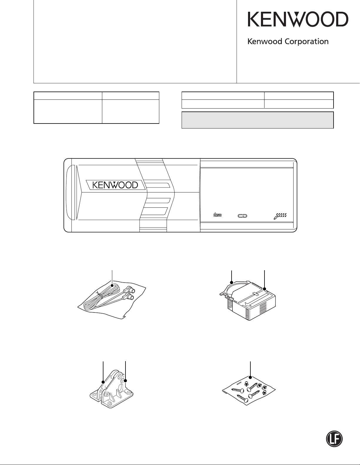
CD AUTO CHANGER
KDC-C719/C719Y
KDC-C719/G4
SERVICE MANUAL
REVISED
© 2006-5 PRINTED IN JAPAN
B53-0418-00 (N) 960
Model
KDC-C719 (E type)
KDC-C719 (K,M type)
KDC-C719/G4 (M type)
Serial Number
U0400251~
60400351~
67400651~
Cord with plug
(E30-4291-15)
Service jig
For initial position setting
When transporting these models, always attach CAUTION
CARD and STEPPED SCREW (for transportation).
COMPACT DISC AUTO CHANGER KDC-C719
NEW ANTI VIBRATION MECHANISM DISC NAME PRESET
COMPACT
CD-R/RW
DIGITAL AUDIO
Tray
(J99-0614-01)
TEXT
Holder assy
(J19-5146-02)
DISC
10
Parts No.
W05-0635-00
5m
Bracket (L)
(J19-5018-03)
Products for European market comply with the
Bracket (R)
(J19-5019-03)
RoHS
Directive.
Screw set
(N99-1784-05)
This product uses Lead Free solder.
Page 2
KDC-C719/C719Y
KDC-C719/G4
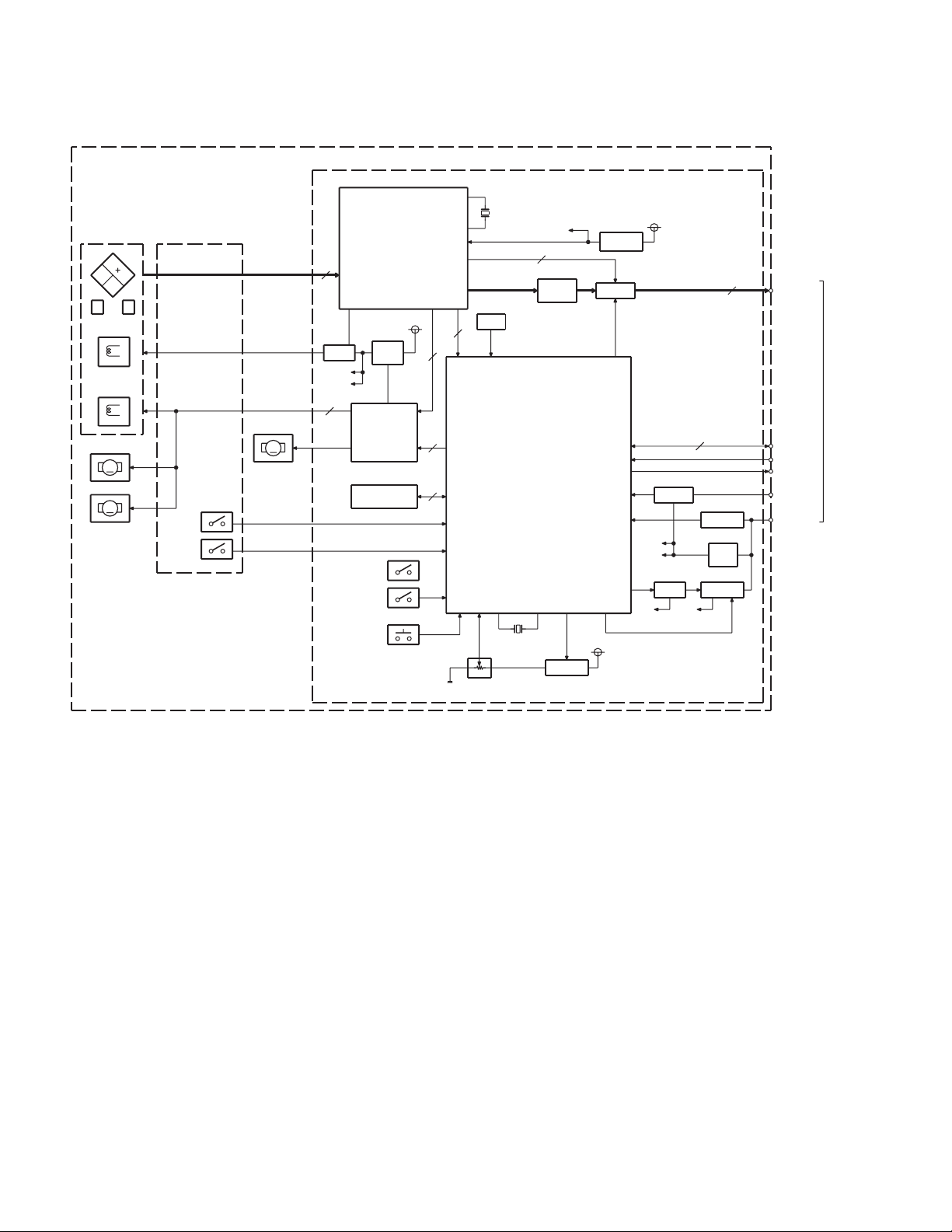
(X92)
PICKUP
ASSY (X16-339)
PD
C
DA
B
EF
FO COIL
TR COIL
SPINDLE
M
SLED
M
LOE SW
LIM SW
ELEVATOR
M
(X32)
7
Q1
SD5V
8
BLOCK DIAGRAM
IC1
X1
16.93MHz
HOT
SYSTEM u-COM
12.5MHz
L.P.S.
APC
SA5V
IC5
BTL &
DC MOTOR
DRIVER
IC8
MG SW
ARM SW
EJ SW
RF AMP &
SERVO DSP &
TEXT DECODER &
D/A CONVERTER &
SCF
S8V
Q9
SA5V
AVR
E2PROM
S1
S3
S2
4
5
2
13
S8V
Q6-8
M5V1
IC4
5VREG
MUTE
IC7
M5V2
7V/8V
M5V1
5
IC9
RESET
Q20
BU. DET
Q21,22
5V
AVR
Q10 Q15,16
P-ON
8V AVR
S8V
3
AUDIO
OUT
5L I/F
CH-CON
CH-MUTE
CH-RST
BU14V
to
X16-338
DA5V
2
Q4,5
0bit
MUTE
X2
Q12
AVREF0
2
Page 3
KDC-C719/C719Y
KDC-C719/G4
COMPONENTS DESCRIPTION
● CD PLAYER UNIT (X32-5810-00)
Ref. No. Application / Function Operation / Condition / Compatibility
IC1 DSP Servo control
IC4 A5V regulator Power supply for 5V audio
IC5 Driver Driving spindle motor, loading/eject operation, elevation operation, driving pick-up ACT
IC7 µ-com Servo control, LX_BUS communication control
IC8 Memory IC ELV operation parameter, Store servo coefficient
IC9 Reset IC
Q1 Current AMP Adjust the current to be applied to the laser
Q4~8 AMUTE SW AMUTE
Q9 SW SA5V
Q10 PON SW PON
Q11 CH RESET SW CH RESET
Q13 CH control SW
Q14 CH MUTE SW CH MUTE
Q16 SW8V
Q17,18 8V SW
Q19 8V/7V SW 8V/7V switching
Q20 BU5V detection SW BU5V detection
Q21,22 BU5V Supply power to IC7
Q30 Anti-scratch measure
Q31 SW Switching loading, eject, and spindle
MICROCOMPUTER’S TERMINAL DESCRIPTION
● SYSTEM MICROCOMPUTER: 784214YGC132A/784217YGC106A (X32: IC7)
Pin No. Pin Name I/O Application
1 NOR/RW O Disc detection result
2 /TSTB O TEXT data strobe signal
3 P_CON O Power supply control signal for video CH
4 FOK I Focus-ON status signal input
5 /XTALEN O Servo IC oscillation stop signal
6 RST O Servo IC reset terminal
7 SA0 O Servo IC communication address setting
8 SSTB O Servo IC communication strobe
9 VDD Positive power supply voltage connection terminal
10 X2 Oscillator connection terminal 2
11 X1 I Oscillator connection terminal 1
12 VSS GND electric potential connection
13 XT2 Sub clock connection terminal 2
14 XT1 I Sub clock connection terminal 1
3
Page 4

KDC-C719/C719Y
KDC-C719/G4
MICROCOMPUTER’S TERMINAL DESCRIPTION
Pin No. Pin Name I/O Application
15 RESET I Reset
16 FOGUP I Focus gain up terminal
17 MGSW I Magazine switch
18 EJSW I Eject switch
19 COMMSW I 5 line communication new/old switch
20 PACK I TEXT data PACK synch signal
21 CHCON I Changer control input from H/U
22 BUDET I BU power supply detection terminal
23 AVDD A/D converter analog power supply terminal
24 AVREF0 I A/D converter reference voltage input
25 HOT I Temperature rise detection
26 LPS I MD deck up/down position detection
27 LOESW I Loading completion switch
28 LIMSW I Limit switch
29 TOFF I Tracking off mode
30 ADJSEL I Servo auto-adjustment ON/OFF
31 TBANK I Tracking bank switching terminal
32 SIM2 I Model detection terminal
33 AVSS A/D converter standard GND terminal
34 LPSCO O A/D converter reference power supply control
35 AMUTE O Audio mute
36 AVREF1 D/A converter reference power supply
37 SDI I Servo IC communication serial data input
38 SDO O Servo IC communication serial data output
39 SCK O Servo IC communication serial clock output
40 DATAH I Data input from H/U
41 DATAC O Data output from the changer
42 HCLK I/O Communication clock input from H/U
43 REQC O Request of communication with H/U
44 CHMUTE O Audio mute output to H/U
45 TSI I TEXT data input
46 TSO O TEXT data output
47 /TSCK O TEXT clock output
48~71 NC O Not used
72 VSS GND electric potential connection terminal
73,74 NC O Not used
75 PUOK O Pick-up type detection terminal (for production)
76 ELVADJ I MD deck up/down position adjustment mode
77~80 NC O Not used
81 VDD Positive power supply voltage connection terminal
82 PUSEL I Pick-up type detection
83 REQH I Request of communication from H/U
84 SP/LO+ O Spindle/loading control terminal +
4
Page 5
MICROCOMPUTER’S TERMINAL DESCRIPTION
Pin No. Pin Name I/O Application
85 SP/LO- O Spindle/loading control terminal 86 ELV+ O MD up/down control terminal +
87 ELV- O MD up/down control terminal 88 SIM1 I Standard stack CH destination port
89 SEARCH O Search/play switching port
90 TEST1 I Mechanism duration mode
91 TEST2 I Mechanism duration mode
92 8V/7V O Driver IC for mechanism operation power supply voltage control
93 EEPWR I EEPROM writing mode
94 TEST/VPP I Flash ROM program mode
95 SRVSEL I Servo operation mode (no mechanism operation)
96 SLNSA I Sled blind zone ON/OFF terminal
97 SDA I/O EEPROM data input/output
98 SCL O EEPROM clock output
99 PON O PON output
100 ARMSW I Arm switch
KDC-C719/C719Y
KDC-C719/G4
ADJUSTMENT
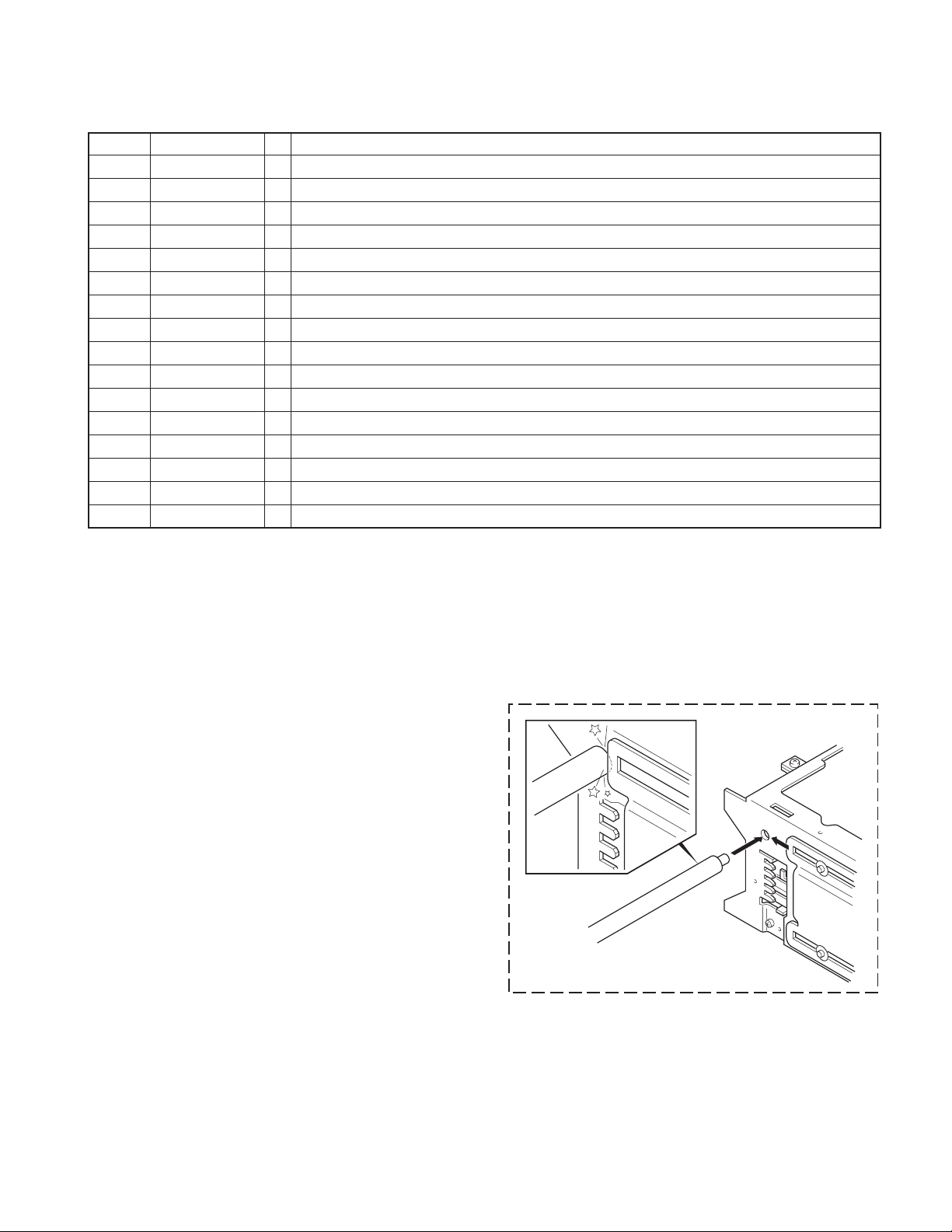
● L.P.S. initial position adjustment procedure
1. Connect the changer to the HEAD UNIT (H/U).
2. While holding the magazine eject button of the changer,
press the reset button of the H/U.
3. After about 3 seconds, release the magazine eject button.
4. Press the SRC button of the H/U to enter the CD-CH mode,
and the H/U's display section indicates “E-88”.
5. Move the mechanism deck to around the 1st stage b y pressing the DISC- or DISC+ button.
6. Insert the adjustment tool (W05-0635-00) into the tool hole
on the changer mechanism.
7. Then press the DISC+ button to move the mechanism dec k
until the mechanism's slider hits the adjustment tool.
8. When the motor locks (stops), press the REPEAT key of
the H/U.
When the REPEAT key is pressed, the mechanism moves
automatically to the 1st stage and the initial position adjustment completes. (The data is written in the EEPROM at
this time.)
W05-0635-00
● Caution : Note on IC8 (EEPROM)
Be sure to use the W05-1306-00 when replacing the
EEPROM. IC8 stores the digital ser vo data of the pickup
servo.
Therefore, if the EEPROM does not store servo data, ERROR76 (E-76) will indicate the H/U’ s display section at the
moment CD is played.
5
Page 6
A B C D E
KDC-C719/C719Y
KDC-C719/G4
1
PC BOARD (COMPONENT SIDE VIEW)
CD PLAYER UNIT X32-5810-00 (J76-0139-11)
F+
T+
T-
F-
SP-
SP+
SL-
SL+
D24
SPLO-
R123
R122
/TSCK
R105
RMK
119
R162
C71
TSO
AVR0 LPS
TSI
GND
SI
50 26
51
IC7
75
76 100
SRVSEL
VPP
TS2
(ELV+)
SIM1
EEP
TS1
SRH
(ELV-)
R856
R854
R857
R855
D7
C61
R77
D11
D3
R102
D12
SGND
(QH)
CP3
TBANK
R505
SLNSA
ELV-
ELV+
8/7V
D15
TOFF
SCL
SDA
R502
ADJSEL
C70
25
1
PON
GND
AM
(DH)
NC
QH
HOT
16
QC
Q8
X1
N/RW
/TSTB
Q18
CCLK
EB
CRST
PACK
BE
DC
R99
CON
R506
DH
D21
D22
X2
VDD
Q17
CN1
L-CH
R78
R54
R-CH
R53
GND
B14V
LIMSW
ROUT
LOUT
Q16
BE
8V
23
LOESW
R73
R72
D16
/RST
RFOK
A0
/STB
S
/SCK
C15
X1
C17
EMPH
SD5V
D9
D10
SI
C16
26
FLAG
ARMSW
E
TX
F
HOLD
VC
IOP-
LD
PD
IOP+
R7
PN
1
IC1
502551
Q21
EBEB
Q22
BASE
D8
CN2
R
L
(CM)
C52
RST
R507
C68
CCON
IGO
IC4
R97
C69
5V
AGND
EB EB
R106
2
C72
CRST
Q6
Q7
EB
1
43
B14V
AMUTE
AGND
DAVDD
R206
Q11
R96
IC9
AVDD
C63
R79
GND
CM
EB
2
R69
IC5
20 38 1
R68
R70
R67
D23
COMMSW
BE
Q31
3
BDET
R76
EJSW
EB
4
Q20
SPLO+
R127
PSL
ELVADJ
R133
5
R5
(LD)
C1D2
100
1
C2D1
A
B
C2D3
PLCK
C3
TE2
C4
LOCK
C5
C
D
TE0
C2D2
(E)
C1D1
VR
R11
R12
R13
R14
FE0
R59
C6
MIRR
R4
(F)
76
75
ATEST
RFCK
(A)
(C)
C9
DAC3
DAC1
(B)
(D)
C7
RF0
C10
DAC2
R87
C11
DAC0
TSTB
PACK
R84
R16
TSI
SA5V
C8
C19
AGC
EFM
R851
GND
ASY
MD
SD
TD
FD
/TSCK
TS
MGSW
C851
6
X32-5810-00
Ref. No. Address
IC1 3D
IC4 3C
IC5 2B
IC7 4B
IC9 4C
Q6 3C
Ref. No. Address
Q7 3C
Q8 3C
Q11 4C
Q16 5D
Q17 5C
Q18 5C
Ref. No. Address
Q20 4A
Q21 5D
Q22 5D
Q31 3A
7
Refer to the schematic diagram for the values of resistors and capacitors.
6
Page 7

JIHGF
KDC-C719/C719Y
KDC-C719/G4
PC BOARD (FOIL SIDE VIEW)
CD PLAYER UNIT X32-5810-00 (J76-0139-11)
C46
C24
R93
R61
R205
R60
C48
C49
R57 R58
C47
C300
C301
C853
R853
S3
R85
D1
Q30
BE
R120
C23
R15
C205
C13
R19
C12
R18
C204
C200
CP16
S1
C75
C201
R20
C206
R9
C2
C202
R10
Q1
EB
R8
C14
C203
L2
R82
CP9
C34
Q13
R95
C85
R100
BE
R81
BE
Q10
EB
1
R25
BE
R71
C55
R26
R161
R17
BE
R101
Q14
R121
R107
D4
R83
R108
R75
R74
R98
IC8
58
R153
R154
R148
TH1
R149
14
R150
C67
CP17
R155
VR1
R156
CP1
R503
Q5
EB
Q4
R80
R110
R111
R22
R190
C56
R21
C21
R852
Q9
C192
R191
R114
R86
C852
S2
2
3
4
C62
R124
C60
C59
D14
Q32
BE
Q19
D5
E
B
X32-5810-00
Ref. No. Address
IC8 4H
Q1 2G
Q4 3H
Q5 3H
Q9 2J
Ref. No. Address
Q10 4H
Q13 3H
Q14 2H
Q19 5H
Q30 2F
Refer to the schematic diagram for the values of resistors and capacitors.
C640
5
C64
6
7
7
Page 8

K L M N O
KDC-C719/C719Y
KDC-C719/G4
1
PC BOARD (COMPONENT SIDE VIEW)
SUB-CIRCUIT UNIT X16-3380-00 (J76-0144-12)
2
13
1211
9
10
8
56
7
1
3
4
2
2
J1
1
16
15
CN1
PC BOARD (FOIL SIDE VIEW)
3
SUB-CIRCUIT UNIT X16-3380-00 (J76-0144-12)
CH-RST
CH-MUTE
CH-CON
CH-CLK
L-CH
R-CH
BU14V
DATAH
AGND
REQC
DATAC
REQH
GND
4
SUB-CIRCUIT UNIT X16-3390-00 (J76-0145-11)
CN1
1
LIMSW
5
R1
R2
6
MGND
SL+
CN2
23
1
16
SP-
SP+
BLACK
RED
SL-
SW1
LOESW
SW2
7
Refer to the schematic diagram for the values of resistors and capacitors.
8
Page 9

A B C D E
D2
KDC-C719/C719Y
KDC-C719/G4
1
2
3
4
5
6
BU14V
CH-CON
CH MUTE
A GND
CH RST
DATAC
DATAH
CH CLK
(OUTSIDE VIEW)
2SB1565
DTA124EK
DTA143EK
DTC114YUA
DTC124EK
DTC343TK
2SB1295-E
(X16-3380-00)
J1
REQH
1
GND
2
3
4
5
6
7
R ch
8
REQC
9
10
11
L ch
12
13
J1
3
2
4
7
6
8
11
10
12
13
(E56-0865-05)
TP2
1
2
3BU+14V
4
1
5 CH MUTE
5
6A GND
9
8
9
10
11
12 L ch
2SC4081
DTA124EUA
DTA143EUA
DTC124EUA
DAN202K
DAN202U
TP14
TP3
TP7
TP8
TP6
TP12
TP4
TP5
TP11
TP10
TP13
TP9
TP1
REQH
GND
CH CON
CH RST7
R ch
REQC
DATAC
DATAH
CH CLK13
1
2
3
4
5
6
7
8
9
10
11
12
13
14
15
16
CN1
CH RST
A GND
CH CON
CH MUTE
CH-CLK
LPS
VR1
BU14V
BU14V
Rch
Lch
GND
GND
DATAH
DATAC
REQC
REQH
NC
10K
CN2
(X32-5810-0x)
2.2
C71
B14V
1
2
CRST
3
R
4
AGND
5
L
6
CCON
7
GND
8
GND
9
CM
10
DH
11
DC
12
CCLK
13
QC
14
QH
15
NC
16
C640
1
R100
1K
AVREF0
LPS
GND
+
220u16
Q20,21
Q18
R503
44
40
41
42
43
83
14.4V
D11
BU 5V
AVR
Q17
2
3
0
7
AGND
D12
1
Q21
+
C64
22K
R124
220u16
4.7
C60
Q17,18
SVR 8V
SW
8/7V
BU DET
DETECT
Q22
D8
R79
3.3K
R61
100
C49
680P
C48
680P
R60
100
R77
18K
0.1
C61
A. MUTE
DRIVE
C59
100u16
D5
BASE
Q19
Q6,7
R57
R58
D7
D10
D9
+
C75(X92-)
(X92-)
7/8V
SW
A. MUTE
10u50
22K
22K
10u50
Q20
Q8
0.047F5.5
Q32
Q16
2
LOUT
Lch
C47
R54
680
R53
680
5V
AVDD
4.7
R78
ROUT
5V AVR
IC4
IN
AVDD
C62
100K
GND
AGND
DAVDD
OUT
8VB14V
100u16
Lch
48
49
Rch
DAVDD
5.0V
10
C34
0V
5V
2.2
2.2
C72
C85
8V
+
6
C70
100P
1
83
+
D21
Q6
D22
Q7
C46
+
Rch
AM
7.0V
C52
+
SRV 8V
AVR
D14
4.7
C63
DAVDD
CRST
R97
3
Q13
7
CH CON
SW
R76
27
28
CP3 100K
R105
1K
R106
1K
D4
100K
R502
R148
100
R149
100
TODF
ADJSEL
TBANK
0
100K
R98
10K
5.0V
5.0V
5.0V
5.0V
0V
SI
(DH)
AVDD
35
37
R111
100K
38
39
R107
100
40
R108
41
42
R99
HOT
TH1
0V
25
26
LPS
27
LOESW
28
LIMSW
29
TOFF
30
ADJSEL
31
TBANK
32
SIM2
33
AVSS
34
LPSCO
35
AMUTE
36
AVREF1
37
SDI
38
SDO
39
SCK
40
DATAH
41
DATAC
42
HCLK
3.9K
0.1
C69
100K
20
R95
100K
BDET
CON
PACK
0V
0V
5.0V
5.0V
5.0V
24
23
HOT
AVDD
AVREF0
0V
0V
22
BUDET
21
CH-CON
20
PACK
D15
R150
1K
0V
43
R121
44
Q14
10K
45
R110
100K
46
47
(CM)
5.0V
CH MUTE
SW
TSI
TSO
TSCK
5.0V
43
REQC
44
CHMUTE
45
TSI
0V
0V
46
TSO
47
TSCK
48
A0
49
A1
50
A2
D0
A3
51
A4A6A7
52
53
D1
A5
565558
54
57
7
2SB1202-E
DAP202K
DAP202U
DA204U
5V
AVDD
8V
VCC
X32-5810-00 (1/3), X16-3380-00 (1/1)
9
Page 10

F G H I J
0V
V
O1
I3-
A6
BUDET
SD
64
13
SP
KDC-C719/C719Y
KDC-C719/G4
R97
3.9K
CON
5.0V
21
CH-CON
A7
0.1
C69
R95
PACK
D0
565558
57
20
10K
100K
R114
COMMSW
0V
5.0V
201918
PACK
D3
D1
D2
60
59
RESET
SW
18
0V
5.0V
17
EJSW
COMMSW
(X32-5810-0x)
D4
D5
61
62
Q11
16
R507
RST
17
0V
5.0V
MGSW
RESET
FOGUP
∗
IC7
SYSTEM u-COM
UNIT
No.
784217YGC106A
0-00
784214YGC132A
0-01
A8
D7
D6
636665
64
L+
56
0V
R190
22K
19
201718
L-
DGND4
TSTB
57
TSTB
CP16
1K
2
R69
30K
AI1
680P
C192
C16
0.1
R-
58
8V
R+
TEST0
59
ATEST
SD5V
16
21
2.5V
R191
5.0V
DAVDD2
TEST1
60
0V
2.5V2.1V2.1V
I1
I2
22
2.5V
12K
DAVDD
Lch
16
L OUT
ATEST
61
I2-
C300
AGND
C301
15
DAGND2
2.5V0V
2.5V
2.5V
AGND1
62
L2
600
7.0V
151413
VCC1
I2+
I3
23
24
2.5V
2.5V
22
0.1
FD
63
TDFDSD
62
SP+
R21
12K
C21
680P
SER
5V
14
REGC
TD
64
12K
R26
63
SP+
3.3V
3.3V
O1-
25
2.5V
18K
R22
2 2
5V
MGSW
R84
17
2
TSTB
0V
2
1
TSTB
NOR/RW
ARMSW
PON
SDA
SLNSA
SRVSEL
TEST/VPP
EEPWR
TEST2
TEST1
SEARCH
SIM1
ELV-
ELV+
SPLO-
SPLO+
REQH
PUSEL
VDD
ASTB
WAIT
ELVADJ
N/RW
SCL
8/7
WR
RD
18
ARMSW
6
1K
4.7K
47K
R87
0.1
C851
EJSW
R83
1K
4.7K
R852 R851
47K
R86
0.1
C852
4.7K
R853
47K
R85
0.1
C853
1K
R82
R155
100
5
5.0V
R156
6
5.0V
0V
100
7
R153
4.7K
5.0V
8
R154
4.7K
5.0V
100
5.0V
99
SCL
5.0V
98
97
0V
96
SLNSA
95
SRVSEL
EEP
94
93
92
91
90
89
SRH
88
87
86
85
84
5.0V
83
5.0V
82
5.0V
81
80
79
78
77
5.0V
76
ELVADJ
5V
AVDD
8V
VCC
C67
0.1
PON
SDA
TS1 TS2
87
86
85
84
PSL
R133
100K
CP1
100K
R505
0
VPP
CP17
100K
SIM1
3 3
(QH)
D3
100K
R102
R127
10K
VDD
R506
0
RESET IC
IC9
IN
3
0V
4
C68
0.1
0
12.500MHz
0V
0V
14
131615
12
XT1
XT2
VSS
IC7
A10
A11
A9
68
67
5.0V
2
R96
OUT
1
X2
X1
9
10
11
X1
X2
5.0V
A13
A12
69
100K
5.0V
VDD
4
5
7
8
1K
CP9
0V
0V
0V
0V
0V
7
643
5
8
VDD
A14
70
RST
SAO
FOK
SSTB
A15
VSS
71
72
0V
P-CON
XTALEN
0V
0V
0V
A17
A16
RAMOK
73
75
74
RMK
R101
1K
SDA
SCL
WP
VCC
E2PROM
IC8
GND
R80
1K
S1
MG
SW
S2
EJ
SW
S3
ARM
SW
0V
4
3
A2
2
A1
1
A0
Q10
R81
10K
P-ON
5V
5V
VCC
VDD
VDD
48,49
6
C203
0.1
6
C201
6
0.1
0bit
MUTE
16
R10
100K
SD5V
C14
0.1
24
XTAL
TSO
53
0V
TSCK
TSO
45
2.5V
23
22
XTAL
16.934MHz
5V
0V
5V
0V
0V
TSI
54
TSI
46
R68
120K
191817
BI1-
BI1+
20
2.5V
63
62
64
XVDD
55
5.0V
AI1+
9.1K
5.0V
21
TSCK
47
R71
0V
X1
16.934MHz
25
XGND
26
5.0V
DVDD1
27
EMPH
EMPH
28
FLAG
FLAG
29
DIN
30
DOUT
31
SCKIN
32
SCKO
33
LRCKIN
34
LRCK
35
HOLD
HOLD
36
TX
TX
37
0V
R20
100K
0V
48
49
R9
1K
6
LOCK
RFCK
PLCK
Q4
Q5
MIRR
C1D1
C1D2
C2D3
3.4V
5.0V
65
C17
C2D1
C2D2
0V
2.2
38
39
40
41
42
43
44
45
46
47
48
49
50
C200
MOTOR
DRIVER
DGND2
C16M
LIMIT
DVDD2
LOCK
RFCK
MIRR
PLCK
DGND3
C1D1
C1D2
C2D1
0V
C2D2
0V
C2D3
DVDD3
51
5.0V
0.1
IC5
PACK
52
PACK
20
SD5V
8V
VCC
X32-5810-00 (2/3)
10
Page 11

ONMLK
I2+
AGND
D
KDC-C719/C719Y
KDC-C719/G4
1
D
4
VCC
R11 5.1K
R12 5.1K
R13 5.1K
R14 5.1K
R4
220
R5
47K
R7
47K
F+
T+
TF-
SPSP+
SLSL+
LOESW
R72
100
LIMSW
R73
100
22K
R75
AMUTE
Q30
ECCENTRIC
DISC SW
R854
3 1/2W
R855
3 1/2W
R856
3 1/2W
R857
3 1/2W
PD
VR
VC
F
E
ELV+
ELV-
A
C
B
D
R120
620K
2
3
4
5
6
7
8
9
10
11
12
13
14
15
16
17
18
19
20
21
22
23
A
C
B
D
F
E
4
6
27
R74
2.2K
28
35
0.1
C202
5
C300
C301
151413
DAGND2
2.5V
2.5V
.5V
62
L2
600
7.0V
151413
VCC1
I3
24
2.5V
C15
22
Rch
0V
0.1
12
REGC
R OUT
DAGND
IC1
SERVO IC
0.1V
0V
MD
SD
TD
FD
65
63
64
TDFDSD
MD
12K
R26
R25
636265
64
SP-
SP+
SP+ SP- T- T+
3.3V
3.3V
O1-
O1+
I3-
I3+
25
262728
R21
2.5V
2.5V
12K
C21
680P
18K
R22
SERVO
5V
0.1
2.5V
1K
R206
SISOSCK
5.0V
0V
5.0V
0V
978
10
11
VDD
XTALEN
DAVDD1
DAC2
DAC1
DAC0
666768
69
DAC1
DAC2
DAC0
11K
0.1
C204
T-
T+
0V
3.3V
3.3V
12
11
O2-
O2+
RIN
ROUT
0V
6.2V
5.0V
C55
10
Q9
7
8
393738
STBAORST
0V
6
SI
SO
AO
STB
SCK
5.0V
5V
0V
AVDD1
DAC3
EFM
71
70
R18
R19
10K
33K
DAC3
EFM
0.01
C12
C13
4
F+
3.3V
9
O3-
VOUT
I1SW
31
30
7.0V
2.5V
Q31
10K
R17
30K
R70
4.7
C56
R205
345
3.3V
8
2.8V5.0V
72
0.01
VIN
SW
D16
RST
ASY
F-
O3+
1K
ASY
3.2V
1.8V
C11
32
C24
RFOK
5.0V
C3T
73
6800P
SL- SL+F-F+
2.5V
VIN
I4+
333435
SP/LOD+
SA5V
4
1000P
220K
2
RFOK
2.5V
2.5V
RFI
74
C10
2200P
SL-
3.3V
3.3V
76543
O4-
I4-
R93
2.5V
REFOUT
2.5V
AGCO
75
AGCO
SL+
O4+
I4
R161
R67
120K
0V
1
DGND1
AVDD3
AGND3
TEC
TEO
FEO
AVDD2
AGND2
EQ2
RFO
AGCI
0V
LO+
D24
16K
TE2
TE-
FE-
RF-
EQ1
D23
6
APC
IOP-
R8
10
C2
10
100
5.0V
PN
0V
99
PN
5.0V
98
LD
0V
97
PD
0V
96
C4
95
1500P
94
93
R59
92
270K
91
C6
90
100P
2.5V
89
5.0V
88
2.5V
87
E
2.6V
86
F
85
(C)
D
84
(A)
B
83
(D)
C
(B)
82
A
0V
81
2.3V
80
79
78
C7
77
C9
76
0.22
3.2V
1.8V
1K
7.0V
0V
R123
2
LO-
VCC2
5.0V
4.3V
MT1
36
4.7K
R162
SP/LOD-
85
84
LDIOP+
Q1
D1
C206
R15
100K
(LD)
TE2
TE0
C5
22P
FE0
(E)
E
(F)
C3
F
470P
C
5
A
D
B
R16
5.6K
4P
RF0
GND
SA5V
3
87
86
ELVD-ELVD+
1K
R122
1
REV
FWD
MT2
SGND
38
37
0V
5.0V
SGND
5
0.1
SA5V
C8
15P
C23
4.7
C205
0.1
C19
2.2
KDC-C719/C719Y, KDC-C719/G4
(X16-3390-00)
CN1
CN1
A
1
C
B
D
GND
LD
PD
VR
VC
VCC
F
E
F+
T+
T-
FSP-
SP+
SL-
SL+
LOESW
MGND
LIMSW
TP1
1
TP2
2
TP3
3
TP4
4
5
6
7
8
9
10
11
12
13
14
15
16
17
18
19
20
21
22
23
TP13
TP14
TP15
TP16
TP17
TP18
TP19
TP20
TP21
TP22
TP23
TP5
TP6
TP7
TP8
TP9
TP10
TP11
TP12
R2
0
R1
0
S1
S2
CN2
1
VCC
2
VC
3
GND
4
LD
5
VR
6
PD
7
C+D
8
F
9
B
10
A
11
E
12
GND
13
F+
14
T+
15
T-
16
F-
LOE SW LIM SW
(X92- )
ELEVATOR
M2
MM
SLED
(X32- )
IC1 : UPD63711AGC-A
IC4 : KIA78L05F-P
IC5 : LA6576-E
IC7 :
IC8 : W05-1306-00
IC9 : S-80830CNNB-G
Q1 : 2SB0970
Q4,8 : DTA124EK
Q5 : DTA124EUA
Q6,7 : DTC343TK
Q9,21 : 2SB1202-E
Q10 : 2SB1295-E
Q11,20 : DTC124EK
Q13,18,19,31 : DTC124EUA
Q14 : DTA143EUA
M
Q16,22 : 2SC4081
D1,15 : DAP202K
D3,4,7 : UDZS5.6B
D5 : MAZS0750M
D8 : MAZS0620M
D9,10 : M1F60-5063
D11 : 1SR154-400
D12 : DA204U
D14 : MAZS0910M
D16 : DAP202U
D21,22 : DAN202K
D23,24 : DAN202U
(X92- )
Q32
M4
∗
DTA143EK:Q17
DTC114YUAQ30 :
2SB1565(E,F):
M1
SPINDLE
SIGNAL LINE
GND LINE
B LINE
CAUTION : For continued safety, replace safety
critical components only with manufacturer’s
recommended parts (refer to parts list).
Indicates safety critical components. To reduce the risk of electric shock, leakage-current
or resistance measurements shall be carried
out (exposed parts are acceptably insulated
from the supply circuit) before the appliance is
returned to the customer.
• DC voltages are as measured with a high
impedance voltmeter. Values may vary
slightly due to variations between individual
instruments or/and units.
X32-5810-00 (3/3), X16-3390-00 (1/1)
DPU1
OPTICAL
PICKUP
2
3
4
5
6
7
11
Page 12

KDC-C719/C719Y
KDC-C719/G4
A
B
C
D
E
F
G
H
J
K
L
1
M
N
φ2x3.5
φ2x2.5(BLK)
φ2x5
φ1.7x1.5(BLK)
φ2x6
M1.7x3
M1.7x2.2
φ2x3.5
WASHER
WASHER
WASHER
WASHER
φ2x3(BLK)
φ3.8
φ4
φ3.8
φ3.5
: N09-4126-15
: N09-6392-05
: N86-2005-48
: N09-4189-15
: N09-6155-15
: N09-6390-05
: N39-1722-48
: N09-6108-15
: N19-2105-14
: N19-2058-04
: N19-2080-14
: N19-2028-04
: N09-6391-05
EXPLODED VIEW (CD MECHANISM)
BA
70
52
H
H
7
H
H
H
21
20
L
54
L
H
L
L
18
L
H
x2
H
47
D
61
59
D
63
12
74
55
2
5
68
22
75
13
29
L
3
2
H
K
11
31
K
30
48
H
23
14
M
A
6
17
A
A
M3
40
(X32-)
27
15
19
x2
50
51
36
K
35
K
C75
H
781
H
772
62
Q32
H
C
C
H
H
3
B
76
53
16
34
J
32
37
K
H
49
4
N
x2
FC1
FC2
56
33
73
F
J
39
J
J
25
57
E
26
M2
N
N
69
E
28
x2
24
38
M1
772
(X16-)
780
FPC1
E
58
46
1
G
x2
A
PU1
FPC1
E
x2
FC1
12
Parts with the exploded numbers larger than 700 are not supplied.
Page 13

226
x10
223
215
EXPLODED VIEW (UNIT)
213
214
KDC-C719/C719Y
KDC-C719/G4
DC
203
1
221
M4x17.3
A
φ2x4
B
φ2.6x6 (BLK)
C
2
222
:
N09-6414-05
:
N89-2004-48
:
N89-2606-43
229
227
206
214
BLACK
SILVER
214
214
213
ME1
212
C
C
207
C
3
A
204
205
Parts with the exploded numbers larger than 700 are not supplied.
732
B
731
B
(X16-3380-00)
C
201
C
C
212
211
A
A
13
Page 14

KDC-C719/C719Y
KDC-C719/G4
PARTS LIST
✽ New parts
Parts without Parts No. are not supplied.
Les articles non mentionnes dans le Parts No. ne sont pas fournis.
Teile ohne Parts No. werden nicht geliefert.
A
Ref. No.
N
d
d
Parts No. Description
e
w
KDC-C719/C719Y_C719/G4
201 3D✽A10-5277-01 CHASSIS
201 3D✽A10-5277-01 CHASSIS M3
201 3D
203 1D A01-2881-01 METALLIC CABINET
203 1D A01-2881-01 METALLIC CABINET M3
203 1D
204 3C A21-4047-12 DRESSING PANEL
204 3C A21-4047-12 DRESSING PANEL M3
204 3C A21-4082-02 DRESSING PANEL K1
205 3C A21-4048-12 DRESSING PANEL
✽
A10-5278-01 CHASSIS K1
✽
A01-2882-01 METALLIC CABINET K1
Desti-
nation
M1E2E3
M1E2E3
M1E2E3
M1E2E3
A
Ref. No.
A3D
B2D
C3DN89-2606-43
ME1 2D✽X92-5310-00
N
d
d
Parts No. Description
e
w
✽
N09-6414-05 STEPPED SCREW
✽
N89-2004-48
BINDING HEAD TAPTITE SCREW
BINDING HEAD TAPTITE SCREW
MECHANISM ASSY (CHM-1400W)
SUB-CIRCUIT UNIT (X16-3380-00)
CN1 E41-2245-05 FLAT CABLE CONNECTOR
J1 E56-0865-05 CYLINDRICAL RECEPTACLE
SUB-CIRCUIT UNIT (X16-3390-00) in X92
✽
CN1
CN2 E41-2612-05 FLAT CABLE CONNECTOR
E41-2514-05 FLAT CABLE CONNECTOR
Desti-
nation
205 3C A21-4048-12 DRESSING PANEL M3
205 3C A21-4083-02 DRESSING PANEL K1
206 2C A22-2997-02 SUB PANEL
207 3C A64-2896-01 PANEL K1
207 3C A64-2897-01 PANEL
207 3C A64-2897-01 PANEL M3
- B46-0100-50 WARRANTY CARD
- B46-0182-14 ID CARD E2E3
- B46-0682-00 WARRANTY CARD E2E3
- B58-1236-04 CAUTION CARD
- B58-1411-04 CAUTION CARD E2E3
- B58-1947-00 CAUTION CARD E2E3
- B64-2346-00
- B64-2350-00
-
- B64-2355-00
- B64-2356-00
211 3D B58-1275-04 CAUTION CARD
212 3D D10-4515-03 ARM
213 1C
214 1C D39-0242-05 DAMPER
215 1C E30-4291-15 CORD WITH PLUG
- H02-0827-03 INNER CARTON CASE
- H10-4729-02
- H13-1706-04 CARTON BOARD
- H25-0337-04
- H25-1111-04
- H25-1111-04
- H25-1115-04 PROTECTION BAG K1
-
-
- H54-2598-04 ITEM CARTON CASE E2
221 1C J19-5018-03 BRACKET (L)
222 1C J19-5019-03 BRACKET (R)
223 1C J19-5146-02
226 1C J99-0614-01 TRAY
✽
B64-2351-10 INSTRUCTION MANUAL (ARA) M1M3
✽
B64-2365-10
✽
D10-4516-14 LEVER
✽
H54-2592-14 ITEM CARTON CASE K1E3
✽
H54-2595-14 ITEM CARTON CASE M1M3
INSTRU.MANUAL (ENG,FRE,SPA,POR)
INSTRUCTION MANUAL (ENG,T-CHI)
INSTRUCTION MANUAL (ENG,RUS,POL
INSTRUCTION MANUAL (CZE,HUN,CRO
INSTRUCTION MANUAL (GER,DUT,ITA
POLYSTYRENE FOAMED FIXTURE
PROTECTION BAG (180X300X0.03)
PROTECTION BAG (280X450X0.03)
PROTECTION BAG (280X450X0.03)
HOLDER ASSY (DISC MAGAZINE)
M1E2E3
K1M1M3
K1E3
M1M3
E2
E2
E3
M1E2E3
M3
R1,2 RK73EB2E000JX CHIP R 0.0 J 1/4W
S1,2 S74-0811-05 MICRO SWITCH
CD PLAYER UNIT (X32-5810-00) in X92
C2 CK73EB1A106K CHIP C 10UF K
C3 CC73GCH1H471J CHIP C 470PF J
C4 CK73GB1H152K CHIP C 1500PF K
C5 CC73GCH1H220J CHIP C 22PF J
C6 CC73GCH1H101J CHIP C 100PF J
C7 CC73GCH1H040C CHIP C 4.0PF C
C8 CC73GCH1H150J CHIP C 15PF J
C9 CK73GB1C224K CHIP C 0.22UF K
C10 CK73GB1H222K CHIP C 2200PF K
C11 CK73GB1H682K CHIP C 6800PF K
C12,13 CK73GB1H103K CHIP C 0.010UF K
C14-16 CK73GB1H104K CHIP C 0.10UF K
C17 CK73FB1A225K CHIP C 2.2UF K
C19 CK73FB1A225K CHIP C 2.2UF K
C21 CC73GCH1H681J CHIP C 680PF J
C23 CK73EB1A475K CHIP C 4.7UF K
C24 CK73GB1H102K CHIP C 1000PF K
C34 CK73EB1A106K CHIP C 10UF K
C46,47 CE32BJ1H100M CHIP EL 10UF 50WV
C48,49 CC73GCH1H681J CHIP C 680PF J
C52 CK73EB1A475K CHIP C 4.7UF K
C55 CK73EB1A106K CHIP C 10UF K
C56 CK73EB1A475K CHIP C 4.7UF K
C59 CE32BJ1C101M CHIP EL 100UF 16WV
C60 CK73EB1A475K CHIP C 4.7UF K
C61 CK73GB1H104K CHIP C 0.10UF K
C62 CE32BJ1C101M CHIP EL 100UF 16WV
C63 CK73EB1A475K CHIP C 4.7UF K
C64 CE32BM1C221M CHIP EL 220UF 16WV
C67-69 CK73GB1H104K CHIP C 0.10UF K
C70 CC73GCH1H101J CHIP C 100PF J
C71,72 CK73FB1A225K CHIP C 2.2UF K
C85 CK73FB1A225K CHIP C 2.2UF K
C192 CC73GCH1H681J CHIP C 680PF J
C200-206 CK73GB1H104K CHIP C 0.10UF K
227 2C K24-4055-04 PUSH KNOB
229 1C
14
✽
N99-1784-05 SCREW SET
E2 : KDC-C719Y E3 : KDC-C719 (Europe)
K1 : KDC-C719 (North America)
M1 : KDC-C719 M3 : KDC-C719/G4 (Other Areas)
C300 CK73EB0J226K CHIP C 22UF K
C301 CK73GB1H104K CHIP C 0.10UF K
C640 CE32BM1C221M CHIP EL 220UF 16WV
C851-853 CK73GB1H104K CHIP C 0.10UF K
Indicates safety critical components.
Page 15

PARTS LIST
CD PLAYER UNIT (X32-5810-00) in X92
A
Ref. No.
CN1
CN2
L2 L92-0322-05 CHIP FERRITE
X1 L78-0596-05 RESONATOR
X2 L78-0568-05 RESONATOR
CP1 RK74GB1J104J CHIP-COM 100K J 1/16W
CP3 RK74GB1J104J CHIP-COM 100K J 1/16W
CP9 RK74GA1J102J CHIP-COM 1.0K J 1/16W
CP16 RK74GB1J102J CHIP-COM 1.0K J 1/16W
CP17 RK74GB1J104J CHIP-COM 100K J 1/16W
R4 RK73GB2A221J CHIP R 220 J 1/10W
R5 RK73GB2A473J CHIP R 47K J 1/10W
R7 RK73GB2A473J CHIP R 47K J 1/10W
R8 RK73EB2E100J CHIP R 10 J 1/4W
R9 RK73GB2A102J CHIP R 1.0K J 1/10W
R10 RK73GB2A104J CHIP R 100K J 1/10W
R11-14 RK73GB2A512J CHIP R 5.1K J 1/10W
R15 RK73GB2A104J CHIP R 100K J 1/10W
R16 RK73GB2A562J CHIP R 5.6K J 1/10W
R17 RK73EB2E103J CHIP R 10K J 1/4W
R18 RK73GB2A103J CHIP R 10K J 1/10W
R19 RK73GB2A333J CHIP R 33K J 1/10W
R20 RK73GB2A104J CHIP R 100K J 1/10W
R21 RK73GB2A123J CHIP R 12K J 1/10W
R22 RK73GB2A183J CHIP R 18K J 1/10W
R25 RK73GB2A113J CHIP R 11K J 1/10W
R26 RK73EB2E123J CHIP R 12K J 1/4W
R53,54 RK73GB2A681J CHIP R 680 J 1/10W
R57,58 RK73GB2A223J CHIP R 22K J 1/10W
R59 RK73GB2A274J CHIP R 270K J 1/10W
R60,61 RK73EB2E101J CHIP R 100 J 1/4W
R67 RK73GB2A124J CHIP R 120K J 1/10W
R68 RK73EB2E124J CHIP R 120K J 1/4W
R69,70 RK73GB2A303J CHIP R 30K J 1/10W
R71 RK73GB2A912J CHIP R 9.1K J 1/10W
R72,73 RK73GB2A101J CHIP R 100 J 1/10W
R74,75 RK73GB2A222J CHIP R 2.2K J 1/10W
R76 RK73GB2A104J CHIP R 100K J 1/10W
R77 RK73GB2A183J CHIP R 18K J 1/10W
R78 RK73GB2A104J CHIP R 100K J 1/10W
R79 RK73GB2A332J CHIP R 3.3K J 1/10W
R80 RK73GB2A102J CHIP R 1.0K J 1/10W
R81 RK73GB2A103J CHIP R 10K J 1/10W
R82-84 RK73GB2A102J CHIP R 1.0K J 1/10W
R85-87 RK73GB2A473J CHIP R 47K J 1/10W
R93 RK73GB2A224J CHIP R 220K J 1/10W
R95,96 RK73GB2A104J CHIP R 100K J 1/10W
R97 RK73GB2A392J CHIP R 3.9K J 1/10W
R98 RK73GB2A103J CHIP R 10K J 1/10W
R99 RK73GB2A104J CHIP R 100K J 1/10W
R100,101 RK73GB2A102J CHIP R 1.0K J 1/10W
R102 RK73GB2A104J CHIP R 100K J 1/10W
R105,106 RK73GB2A102J CHIP R 1.0K J 1/10W
R107 RK73GB2A101J CHIP R 100 J 1/10W
E2 : KDC-C719Y E3 : KDC-C719 (Europe)
K1 : KDC-C719 (North America)
M1 : KDC-C719 M3 : KDC-C719/G4 (Other Areas)
N
d
d
Parts No. Description
e
w
✽
E41-2179-05 FLAT CABLE CONNECTOR
✽
E41-2173-05 FLAT CABLE CONNECTOR
Desti-
nation
KDC-C719/C719Y
KDC-C719/G4
A
Ref. No.
R108 RK73GB2A104J CHIP R 100K J 1/10W
R110,111 RK73GB2A104J CHIP R 100K J 1/10W
R114 RK73GB2A103J CHIP R 10K J 1/10W
R120 RK73GB2A624J CHIP R 620K J 1/10W
R121 RK73GB2A103J CHIP R 10K J 1/10W
R122,123 RK73GB2A102J CHIP R 1.0K J 1/10W
R124 RK73GB2A223J CHIP R 22K J 1/10W
R127 RK73GB2A103J CHIP R 10K J 1/10W
R133 RK73GB2A104J CHIP R 100K J 1/10W
R148,149 RK73GB2A101J CHIP R 100 J 1/10W
R150 RK73GB2A102J CHIP R 1.0K J 1/10W
R153,154 RK73GB2A472J CHIP R 4.7K J 1/10W
R155,156 RK73GB2A101J CHIP R 100 J 1/10W
R161 RK73GB2A163J CHIP R 16K J 1/10W
R162 RK73GB2A472J CHIP R 4.7K J 1/10W
R190 RK73GB2A223J CHIP R 22K J 1/10W
R191 RK73GB2A123J CHIP R 12K J 1/10W
R205 RK73EB2E102J CHIP R 1.0K J 1/4W
R206 RK73GB2A102J CHIP R 1.0K J 1/10W
R502 RK73GB2A000JX CHIP R 0.0 J 1/10W
R503 RK73EB2E000JX CHIP R 0.0 J 1/4W
R505-507 RK73GB2A000JX CHIP R 0.0 J 1/10W
R851-853 RK73GB2A472J CHIP R 4.7K J 1/10W
R854-857
S1 S68-0823-05 PUSH SWITCH
S2 S70-0838-05 TACT SWITCH
S3 S68-0823-05 PUSH SWITCH
D1 DAP202K DIODE
D3,4 UDZS5.6B ZENER DIODE
D5
D7 UDZS5.6B ZENER DIODE
D8
D9,10 D1F60-5063 DIODE
D11 1SR154-400 DIODE
D12 DA204U DIODE
D14 MAZS0910M ZENER DIODE
D15 DAP202K DIODE
D16 DAP202U DIODE
D21,22 DAN202K DIODE
D23,24 DAN202U DIODE
IC1 UPD63711AGC-A MOS-IC
IC4
IC5
IC7
IC8 W05-1306-00 ROM IC
IC9 S-80830CNNB-G MOS-IC
Q1 2SB0970 TRANSISTOR
Q4 DTA124EK DIGITAL TRANSISTOR
Q5 DTA124EUA DIGITAL TRANSISTOR
Q6,7 DTC343TK DIGIT AL TRANSIST OR
Q8 DTA124EK DIGITAL TRANSISTOR
Q9
Q10 2SB1295-E TRANSISTOR
Q11 DTC124EK DIGIT AL TRANSIST OR
N
d
d
Parts No. Description
e
w
✽
RK73PB2H3R0J CHIP R 3.0 J 1/2W
✽
MAZS0750M ZENER DIODE
✽
MAZS0620M ZENER DIODE
✽
KIA78L05F-P ANALOGUE IC
✽
LA6576-E ANALOGUE IC
✽
784217YGC106A MICROCONTROLLER IC
✽
2SB1202-E TRANSISTOR
Indicates safety critical components.
Desti-
nation
15
Page 16

KDC-C719/C719Y
KDC-C719/G4
CD PLAYER UNIT (X32-5810-00) in X92
A
Ref. No.
Q13 DTC124EUA DIGITAL TRANSISTOR
Q14 DTA143EUA DIGITAL TRANSIST OR
Q16 2SC4081 TRANSISTOR
Q17 DTA143EK DIGITAL TRANSISTOR
Q18,19 DTC124EUA DIGITAL TRANSIST OR
N
d
d
Parts No. Description
e
w
PARTS LIST
Desti-
nation
Ref. No.
46 2B
47 1B G01-3037-04 EXTENSION SPRING
48 2B G01-3038-04 TORSION COIL SPRING
49 3A G01-3039-04 COMPRESSION SPRING
50 3A G01-3040-04 EXTENSION SPRING
A
d
d
N
Parts No. Description
e
w
✽
G01-3036-14 TORSION COIL SPRING
Desti-
nation
Q20 DTC124EK DIGIT AL TRANSIST OR
Q21
Q22 2SC4081 TRANSISTOR
Q30 DTC114YUA DIGITAL TRANSISTOR
Q31 DTC124EUA DIGITAL TRANSISTOR
TH1
✽
2SB1202-E TRANSISTOR
✽
NCP18WB333J0S THERMISTOR 33K
MECHANISM ASSY (X92-5310-00) (CHM-1400W)
12B
22B
32BA10-4751-13 CHASSIS CALKING ASSY
43A
52A
62A
71A
C75 3A C90-5647-05 ELECTRO 0.047F 5.5WV
11 2B D10-4546-03 ARM
12 2A
13 2B
14 2B
15 3A
16 2A
17 2A
18 1B
19 3A
20 1B
21 1B D10-4547-03 LEVER
22 2B
23 2B
24 3B D13-2185-04 GEAR
25 3B D13-2186-04 GEAR
26 3B D13-2187-04 GEAR
27 3A D13-2188-04 WORM
28 2B D13-2092-04 GEAR
29 2B
30 2B D13-2095-04 GEAR
31 2B D13-2096-04 GEAR
32 3A D13-2099-04 GEAR
33 3A D13-2100-04 GEAR
34 3A D13-2101-04 GEAR
35 3A D13-2102-04 GEAR
✽
A10-4745-23 CHASSIS ASSY
✽
A10-4748-32 CHASSIS CALKING ASSY
✽
A10-4754-14 CHASSIS CALKING ASSY
✽
A10-4757-42 CHASSIS CALKING ASSY
✽
A10-4759-12 CHASSIS
✽
A10-4760-12 CHASSIS CALKING ASSY
✽
D10-4527-13 SLIDER
✽
D10-4528-13 ARM
✽
D10-4529-13 ARM
✽
D10-4531-14 LEVER ASSY
✽
D10-4533-13 LEVER
✽
D10-4534-24 SLIDER ASSY
✽
D10-4536-23 SLIDER
✽
D10-4537-14 SLIDER ASSY
✽
D10-4540-23 ARM
✽
D12-0630-12 CAM
✽
D12-0631-12 CAM
✽
D13-2093-14 GEAR ASSY
51 3A G01-3041-04 EXTENSION SPRING
52 1B G01-3042-04 TORSION COIL SPRING
53 2A G01-3043-04 TORSION COIL SPRING
54 1B G01-3044-04 EXTENSION SPRING
55 2A G01-3045-04 EXTENSION SPRING
56 2A G01-3046-04 EXTENSION SPRING
57 3B G02-1374-04 FLAT SPRING
58 3B G02-1375-03 FLAT SPRING
59 2B G02-1376-03 FLAT SPRING
61 2B G02-1378-14 FLAT SPRING
✽
62 3A
63 2A G10-1045-14 FELT
68 2B J11-0637-03 CLAMPER
69 3B
70 1B
73 2B J90-0759-03 GUIDE
74 2A J90-0992-03 RAIL
75 2B J90-0990-03 GUIDE
FPC1 3B J86-0027-05 FPC (LEAD FREE)
A2A
B3A
C3A
D2B
E3BN09-6155-15
F2B
G3B
H3AN09-6108-15 TAPTITE SCREW (M2X3.5)
J3AN19-2105-14 FLAT W ASHER
K3AN19-2058-04 FLAT W ASHER
L1BN19-2080-14 FLAT WASHER
M2BN19-2028-04 FLA T WASHER
N3A
76 3A✽R33-0207-35
M1 3B✽T42-1337-04 DC MOTOR
M2, 3 3A
Q32 3A 2SB1565(E,F) TRANSISTOR
PU1 3B X93-2010-01 OPTICAL PICKUP ASSY
G02-1380-14 FLAT SPRING
✽
J21-9592-14 MOUNTING HARDWARE
✽
J21-9595-13 MOUNTING HARDWARE
✽
N09-4126-15 TAPTITE SCREW (2X3.5,CT)
✽
N09-6392-05 TAPTITE SCREW (S2X2.5 NI)
✽
N86-2005-48
✽
N09-4189-15 TAPTITE SCREW (1.7X1.5 ST)
✽
N09-6390-05 MACHINE SCREW (M1.7X3)
✽
N39-1722-48 PAN HEAD MACHINE SCREW
✽
N09-6391-05
✽
T42-1063-15 DC MOTOR
BINDING HEAD TAPTITE SCREW
SEMS (TAPTITE SCREW) (PT 2X6)
TAPTITE SCREW (S2X3 BLACK-NI)
SLIDE TYPE V ARIABLE RESISTOR
36 3A D13-2103-04 GEAR
37 3A D13-2104-14 GEAR
38 3B D19-0636-04 LEAD SCREW
39 3A D19-0637-04 CLUTCH ASSY
40 3A D39-0225-05 DAMPER
FC1 3A E39-0172-15 FLAT CABLE
FC2 3A E39-0173-35 FLAT CABLE
E2 : KDC-C719Y E3 : KDC-C719 (Europe)
K1 : KDC-C719 (North America)
M1 : KDC-C719 M3 : KDC-C719/G4 (Other Areas)
16
Indicates safety critical components.
Page 17

PARTS LIST
CAPACITORS
C C 4 5 T H 1 H 2 2 0 J
1234 56
1 = Type ... ceramic, electrolytic, etc. 4 = Voltage rating
2 = Shape ... round, square, etc. 5 = Value
3 = Temp. coefficient 6 = Tolerance
• Temperature coefficient
1st Word C L P R S T U
Color* Black Red Orange Yellow Green Blue Violet
ppm/°C0–80 –150 –220 –330 –470 –750
CC45
Color*
2nd Word G H J K L
ppm/°C ±30 ±60 ±120 ±250 ±500
Example : CC45TH = –470±60ppm/°C
• Capacitor value
010 = 1pF 2 2 0 = 22pF
100 = 10pF
101 = 100pF Multiplier
102 = 1000pF = 0.001µF 2nd number
103 = 0.01µF 1st number
KDC-C719/C719Y
KDC-C719/G4
• Tolerance (More than 10pF)
Code C D G J K M X Z P No code
(%) ±0.25 ±0.5 ±2 ±5 ±10 ±20 +40 +80 +100 More than 10µF : –10~+50
–20 –20 –0 Less than 4.7µF : –10~+75
• Voltage rating
2nd word
1st word
0 1.0 1.25 1.6 2.0 2.5 3.15 4.0 5.0 6.3 8.0 –
11012.5 16 20 25 31.5 40 50 63 80 35
2 100 125 160 200 250 315 400 500 630 800 –
3 1000 1250 1600 2000 2500 2150 4000 5000 6300 8000 –
• Chip capacitors
(EX) C C 7 3 F S L 1 H 0 0 0 J Refer to the table above.
12345 67 1 = Type
(Chip) (CH, RH, UJ, SL) 2 = Shape
(EX) C K 7 3 F F 1 H 0 0 0 Z 4 = Temp. coefficient
12345 67 5 = Voltage rating
(Chip) (B, F) 6 = Value
ABCDEFGHJKV
3 = Dimension
7 = Tolerance
RESISTORS
• Chip resistor (Carbon)
(EX) R D 7 3 E B 2 B 0 0 0 J
12345 67
(Chip) (B, F)
• Carbon resistor (Normal type)
(EX) R D 1 4 B B 2 C 0 0 0 J
12345 67
1 = Type 5 = Rating wattage
2 = Shape 6 = Value
3 = Dimension 7 = Tolerance
4 = Temp. coefficient
(Less than 10pF)
Code B C D F G
(pF) ±0.1 ±0.25 ±0.5 ±1 ±2
• Dimension
L
T
W
Chip capacitor
Code L W T
Empty 5.6±0.5 5.0±0.5 Less than 2.0
A 4.5±0.5 3.2±0.4 Less than 2.0
B 4.5±0.5 2.0±0.3 Less than 2.0
C 4.5±0.5 1.25±0.2 Less than 1.25
D 3.2±0.4 2.5±0.3 Less than 1.5
E 3.2±0.2 1.6±0.2 Less than 1.25
F 2.0±0.3 1.25±0.2 Less than 1.25
G 1.6±0.2 0.8±0.2 Less than 1.0
H 1.0±0.05 0.5±0.05 0.5±0.05
Chip resistor
Code L W T
E 3.2±0.2 1.6±0.2 1.0
F 2.0±0.3 1.25±0.2 1.0
G 1.6±0.2 0.8±0.2 0.5±0.1
H 1.0±0.05 0.5±0.05 0.35±0.05
• Rating wattage
Code Wattage Code Wattage Code Wattage
1J 1/16W 2C 1/6W 3A 1W
2A 1/10W 2E 1/4W 3D 2W
2B 1/8W 2H 1/2W
17
Page 18

KDC-C719/C719Y
KDC-C719/G4
Disc section
Laser diode ........................................................................................................... GaAlAs (λ=780nm)
Digital filter ..................................................................................................... 8 Times Over Sampling
D/A Converter ................................................................................................................................1Bit
Spindle speed ....................................................................................................... 500~200rpm (CLV)
Wow & Flutter.................................................................................................Below Measurable Limit
Frequency response ............................................................................................. 5Hz~20kHz (±1dB)
Total harmonic distortion .............................................................................................. 0.005% (1kHz)
S/N ratio .................................................................................................................................... 100dB
Dynamic range ............................................................................................................................ 94dB
Channel separation ..................................................................................................................... 96dB
General
Operating voltage........................................................................................................14.4V (11~16V)
Current consumption.................................................................................................................... 0.8A
Installation Size (W x H x D) .............................. 250 x 80 x 176 mm (9-13/16 x 3-1/8 x 6-13/16 inch)
Weight ........................................................................................................................... 2.0kg (4.4 lbs)
SPECIFICATIONS
KENWOOD follows a policy of contin uous advancements in development.
For this reason specifications may be changed without notice.
DANGER:
Please do not look the laser beam directly during repair or operation check.
 Loading...