

Kenwood BM 366 Schematic

21-S3-C9484/C9488/F9488-092003
USER'S MANUAL
S3C9484/C9488/F9488
8-bit CMOS
Microcontroller
Revision 1

S3C9484/C9488/F9488 PRODUCT OVERVIEW
1 PRODUCT OVERVIEW
S3C9-SERIES MICROCONTROLLERS
Samsung's SAM88RCRI family of 8-bit single-chip CMOS microcontrollers offers a fast and efficient CPU, a wide
range of integrated peripherals, and various mask-programmable ROM sizes.
A address/data bus architecture and a large number of bit-configurable I/O ports provide a flexible programming
environment for applications with varied memory and I/O requirements. Timer/counters with selectable operating
modes are included to support real-time operations.
S3C9484/C9488/F9488 MICROCONTROLLER
The S3C9484/C9488/F9488 single-chip CMOS microcontrollers are fabricated using the highly advanced CMOS
process technology based on Samsung’s latest CPU architecture.
The S3C9484 is a microcontroller with a 4K-byte mask-programmable ROM embedded.
The S3C9488 is a microcontroller with a 8K-byte mask-programmable ROM embedded.
The S3F9488 is a microcontroller with a 8K-byte multi time programmable ROM embedded.
Using a proven modular design approach, Samsung engineers have successfully developed the
S3C9484/C9488/F9488 by integrating the following peripheral modules with the powerful SAM88 RCRI core:
— Five configurable I/O ports (38 pins) with 8-pin LED direct drive and LCD display
— Ten interrupt sources with one vector and one interrupt level
— One watchdog timer function with two source clock (Basic Timer overflow and internal RC oscillator)
— One 8-bit basic timer for oscillation stabilization
— Watch timer for real time clock
— Two 8-bit timer/counter with time interval, PWM, and Capture mode
— Analog to digital converter with 9 input channels and 10-bit resolution
— One asynchronous UART
The S3C9484/C9488/F9488 microcontroller is ideal for use in a wide range of home applications requiring simple
timer/counter, ADC, LED or LCD display with ADC application, etc. They are currently available in 32-pin SOP/SDIP,
42-pin SDIP and 44-pin QFP package.
MTP
The S3F9488 has on-chip 8-Kbyte multi time programmable (MTP) ROM instead of masked ROM. The S3F9488 is
fully compatible to the S3C9488, in function, in D.C. electrical characteristics and in pin configuration.
1-1

PRODUCT OVERVIEW S3C9484/C9488/F9488
FEATURES
CPU
• SAM88RCRI CPU core
Memory
• 208-byte general purpose register (RAM)
• 4/8-Kbyte internal mask program memory
• 8-Kbyte internal multi time program memory
(S3F9488)
Oscillation Sources
• Crystal, Ceramic, RC
• CPU clock divider (1/1, 1/2, 1/8, 1/16)
Instruction Set
• 41 instructions
• IDLE and STOP instructions added for power-
down modes
Instruction Execution Time
• 500 ns at 8-MHz f
(minimum)
OSC
Interrupts
• 10 interrupt sources with one vector / one level
I/O Ports
• Total 38 bit-programmable pins (44QFP)
Total 36 bit-programmable pins (42SDIP)
Total 26 bit-programmable pins (32SDIP/32SOP)
LCD Controller/Driver (Optional)
• 8 COM × 19 SEG (MAX 19 digit)
4 COM × 19 SEG (MAX 8 digit)
A/D Converter
• Nine analog input channels
• 12.5us conversion speed at 4MHz f
ADC
clock.
Asynchronous UART
• Programmable baud rate generator
• Support serial data transmit/receive operations
with 8-bit, 9-bit UART
Watchdog Timer
• Two oscillation sources selection
(by Smart option)
• Safety work for noise interference
Low Voltage Reset (LVR)
• Low Voltage Check to make system reset
• V
= 2.6V/3.3V/3.9V
LVR
Voltage Detector for Indication
• Voltage Detector to indicate specific voltage.
• S/W control (2.4V, 2.7V, 3.3V, 3.9V)
Operating Temperature Range
• –25
°
C to + 85°C
Basic Timer
• One programmable 8-bit basic timer (BT) for
Oscillation stabilization control •
8bit Timers A/B
• One 8-bit timer/counter (Timer A) with three
operating modes; Interval mode, capture mode
and PWM mode.
• One 8-bit timer/counter (Timer B) Carrier
frequency (or PWM) generator.
Watch Timer
• Real-time and interval time measurement.
• Four frequency output to BUZ pin.
• Clock generation for LCD.
1-2
Operating Voltage Range
• 2.2V to 5.5 V at 4 MHz f
• 2.7V to 5.5 V at 8 MHz f
OSC
OSC
Package Type
• 32-pin SDIP, 32-pin SOP
• 42-pin SDIP, 44-pin QFP
Smart Option
• Low Voltage Reset(LVR) level and enable/disable
are at your hardwired option.
• I/O Port (P0.0- P0.2/P3.3-P3.6) mode selection at
Reset.
• Watchdog Timer oscillator selection.
S3C9484/C9488/F9488 PRODUCT OVERVIEW
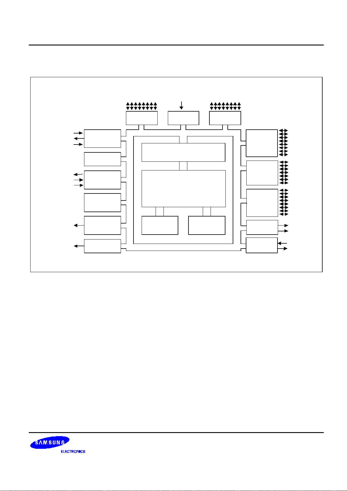
BLOCK DIAGRAM
XIN, XT
X
OUT
, XT
RESET (P0.2)
TAOUT(P3.4)
TACK(P3.5)
TACAP(P3.6)
TBPWM(P1.0)
BUZ(P1.1)
OUT
P0.0-P0.7
(ADC4-8/COM4-7) AV
Port 0 Port 1A/D
IN
OSC/RESET
8-Bit
Basic Timer
8-Bit
Timer
/Counter A
Watchdog
Timer with RC
oscillator
8-Bit
Timer
/Counter B
Watch Timer
I/O Port and Interrupt Control
SAM88RCRI CPU
8-Kbyte
ROM
REF
208-Byte
P1.0-P1.7
(ADC0-3, COM0-3)
RAM
Port 2
Port 3
Port 4
LCD
Driver
UART
P2.0-P2.7
(SEG3-10)
P3.0-P3.6
(SEG15-18,
INT0-3)
P4.0-P4.6
(SEG0-2,
SEG11-14)
COM0-7
SEG0-18
TXD(P3.2)
RXD(P3.1)
Figure 1-1. S3C9484/C9488/F9488 Block Diagram
1-3

PRODUCT OVERVIEW S3C9484/C9488/F9488
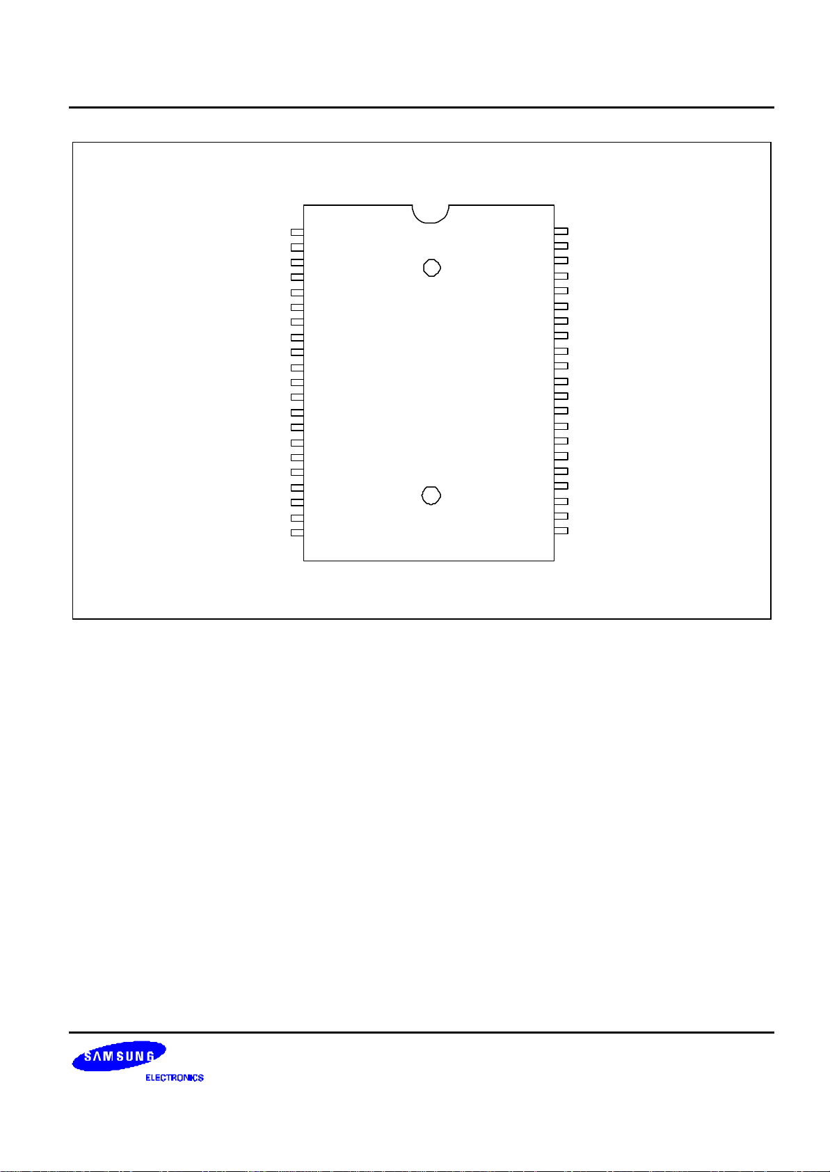
PIN ASSIGNMENT
P2.3/SEG6
P2.2/SEG5
P2.1/SEG4
P2.0/SEG3
P4.2/SEG2
P4.1/SEG1
P4.0/SEG0
P1.7/COM0
P1.6/COM1
P1.5/COM2
P1.4/COM3
3332313029282726252423
SEG7/P2.4
SEG8/P2.5
SEG9/P2.6
SEG10/P2.7
SEG11/P4.3
SEG12/P4.4
SEG13/P4.5
SEG14/P4.6
SEG15/P3.0
SEG16/RXD/P3.1
SEG17/TXD/P3.2
34
35
36
37
38
39
40
41
42
43
44
S3C9484
S3C9488
S3F9488
(Top View)
(44-QFP)
1234567891011
22
21
20
19
18
17
16
15
14
13
12
P1.3/ADC0
P1.2/ADC1
P1.1/ADC2/BUZ
P1.0/ADC3/TBPWM
P0.7/COM4/ADC4
P0.6/COM5/ADC5
P0.5/COM6/ADC6
AVREF
P0.4/COM7/ADC7
P0.3/ADC8
P0.2/RESETB
XIN
VSS
VDD
XOUT
TEST
XTIN/P0.0
XTOUT/P0.1
TACK/INT2/P3.5
SEG18/INT0/P3.3
TACAP/INT3/P3.6
TAOUT/INT1/P3.4
Figure 1-2. S3C9484/C9488/F9488 Pin Assignment (44-QFP)
1-4
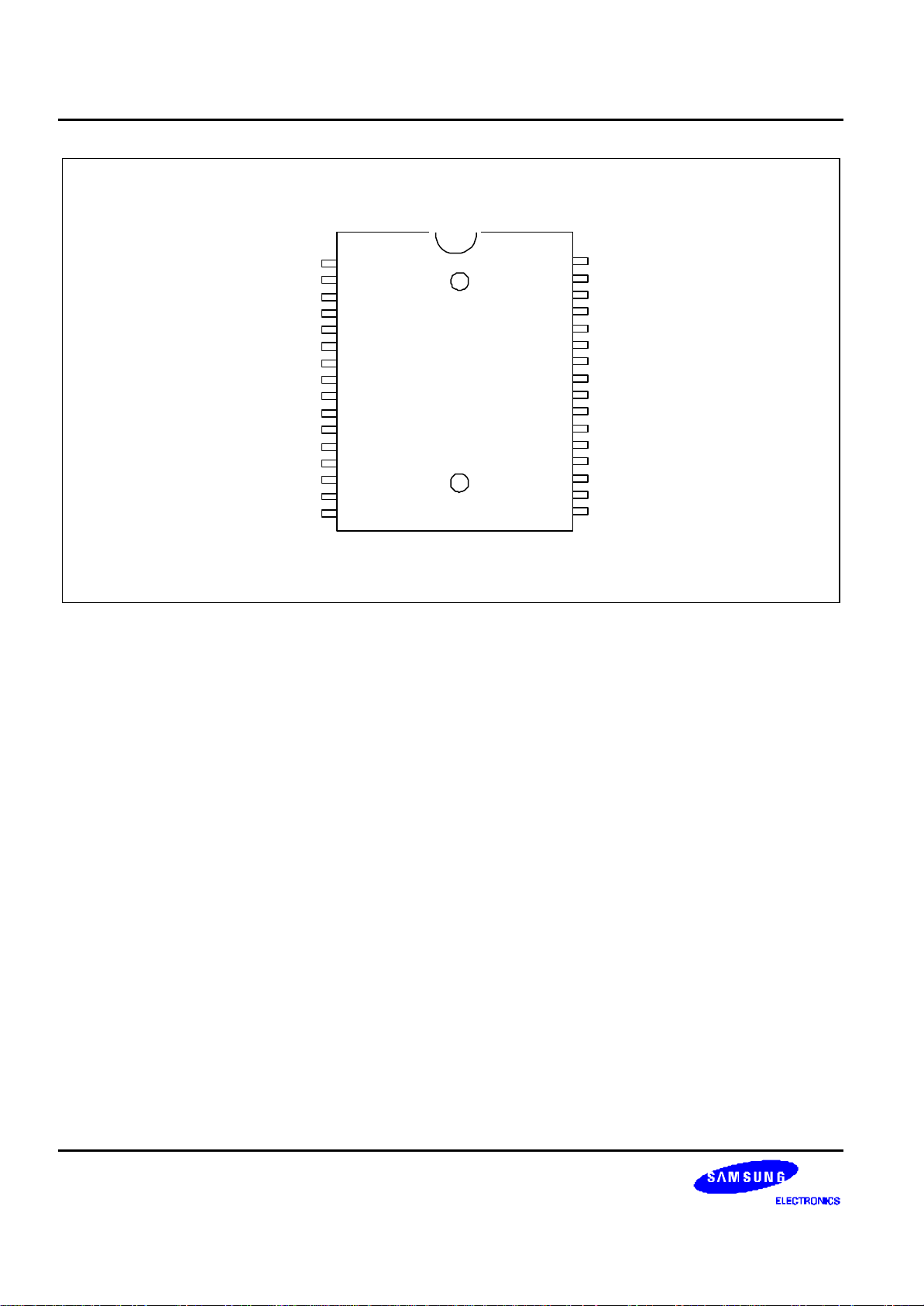
S3C9484/C9488/F9488 PRODUCT OVERVIEW
SEG12/P4.4
SEG13/P4.5
SEG14/P4.6
SEG15/P3.0
SEG16/RXD/P3.1
SEG17/TXD/P3.2
SEG18/INT0/P3.3
TAOUT/INT1/P3.4
TACK/INT2/P3.5
TACAP/INT3/P3.6
VDD
VSS
XOUT
XIN
TEST
XTIN/P0.0
XTOUT/P0.1
RESETB/P0.2
AVREF
COM6/ADC6/P0.5
COM5/ADC5/P0.6
1
2
3
4
5
6
7
8
9
10
11
12
13
14
15
16
17
18
19
20
21
S3C9484
S3C9488
S3F9488
(Top View)
42-SDIP
42
41
40
39
38
37
36
35
34
33
32
31
30
29
28
27
26
25
24
23
22
P4.3/SEG11
P2.7/SEG10
P2.6/SEG9
P2.5/SEG8
P2.4/SEG7
P2.3/SEG6
P2.2/SEG5
P2.1/SEG4
P2.0/SEG3
P4.2/SEG2
P4.1/SEG1
P4.0/SEG0
P1.7/COM0
P1.6/COM1
P1.5/COM2
P1.4/COM3
P1.3/ADC0
P1.2/ADC1
P1.1/ADC2/BUZ
P1.0/ADC3/TBPWM
P0.7/ADC4/COM4
Figure 1-3. S3C9484/C9488/F9488 Pin Assignment (42-SDIP)
1-5
PRODUCT OVERVIEW S3C9484/C9488/F9488
VSS
XOUT
XIN
TEST
XTIN/P0.0
XTOUT/P0.1
RESETB/P0.2
AVREF
ADC3/TBPWM/P1.0
BUZ/ADC2/P1.1
ADC1/P1.2
ADC0/P1.3
COM3/P1.4
COM2/P1.5
COM1/P1.6
COM0/P1.7
1
2
3
4
5
6
7
8
9
10
11
12
13
14
15
16
S3C9484
S3C9488
S3F9488
(Top View)
32-SOP
32-SDIP
32
31
30
29
28
27
26
25
24
23
22
21
20
19
18
17
VDD
P3.6/INT3/TACAP
P3.5/INT2/TACK
P3.4/INT1/TAOUT
P3.3/INT0/SEG18
P3.2/TXD/SEG17
P3.1/RXD/SEG16
P3.0/SEG15
P2.7/SEG10
P2.6/SEG9
P2.5/SEG8
P2.4/SEG7
P2.3/SEG6
P2.2/SEG5
P2.1/SEG4
P2.0/SEG3
Figure 1-4. S3C9484/C9488/F9488 Pin Assignment (32-SOP/SDIP)
1-6
S3C9484/C9488/F9488 PRODUCT OVERVIEW
PIN DESCRIPTIONS
Table 1-1. Pin Descriptions of 44-QFP and 42-SDIP
Pin
Names
P0.0, P0.1
P0.2
P0.3
P0.4
P0.5
Pin
Pin Description Circuit
Type
I/O I/O port with bit-programmable pins.
Configurable to input or push-pull output
mode. Pull-up resistors can be assigned
by software. Pins can also be assigned
individually as alternative function pins.
P0.6
P0.7
P1.0
P1.1–P1.3
P1.4–P1.7
I/O I/O port with bit-programmable pins.
Configurable to input or push-pull output
mode. Pull-up resistors can be assigned
by software. Pins can also be assigned
individually as alternative function pins.
P2.0–P2.7 I/O I/O port with bit-programmable pins.
Configurable to input mode, push-pull
output mode. Input mode with pull-up
resistors can be assigned by software.
The port 2 pins have high current drive
capability. Pins can also be assigned
individually as alternative function pins.
P3.0–P3.2
P3.3
P3.4, P3.6
P3.5
I/O I/O port with bit-programmable pins.
Configurable to input or push-pull output
mode. Pull-up resistors can be assigned
by software. Pins can also be assigned
individually as alternative function pins.
P4.0–P4.6 I/O I/O port with bit-programmable pins.
Configurable to input mode, push-pull
output mode. Input mode with pull-up
resistors can be assigned by software.
Pins can also be assigned individually as
alternative function pins.
44 Pin
Type
E
E-1
E-2
No.
10–14
16–18
H-16
E-3
19–26
E-1
H-14
H-14
H-14
H-15
30–37
42–44,
1–4
H-17
D-5
D-4
H-14 27–29
38–41
42 Pin
No.
16–18
20-22
Shared
Functions
XTIN, XT OUT
RESETB
ADC8
COM7/ADC7
COM6/ADC6
COM5/ADC5
COM4/ADC4
23–30 ADC3/TBPWM
ADC2/BUZ
ADC1–ADC0
COM3–COM0
34–41 SEG3–SEG10
4–10 SEG15
SEG16/RXD
SEG17/TXD
SEG18/INT0
TAOUT/INT1
TACK/INT2
TACAP/INT3
31–33
42, 1–3
SEG0–2
SEG11–14
XIN, X
OUT
I, O System clock input and output pins – 8,7 14,13 –
TEST I Test signal input pin (for factory use only;
must be connected to VSS.)
V
DD
V
SS
– Power supply input pin – 5 11 –
– Ground pin – 6 12 –
_ 9 15 _
1-7
PRODUCT OVERVIEW S3C9484/C9488/F9488
Table 1-1. Pin Descriptions of 44-QFP and 42-SDIP (Continued)
Pin
Names
SEG0–18
Pin
Pin Description Circuit
Type
O LCD segment display signal output pins H-14
Type
H-15
44 Pin
No.
42 Pin
No.
27–44,131–42,
1–7
H-17
COM0–7 O LCD common signal output pins H-14
H-16
26–23
18–16
30–27
20–22
14
ADC0–8 I A/D converter analog input channels E-1
E-3
H-16
22–20
19
18-14
20–26 P1.3–P1.2
13
AVREF I A/D converter reference voltage 15 19
RXD I/O Serial data RXD pin for receive input and
H-17 43 5 P3.1/SEG16
transmit output (mode 0)
Shared
Functions
P4.0–P4.2
P2.0–P2.7
P4.3–P4.6
P3.0
P3.1/RXD
P3.2/TXD
P3.3/INT0
P1.7–P1.4
P0.4–P0.7
P1.1/BUZ
P1.0/TBPWM
P0.7/COM4
P0.6/COM5
P0.5/COM6
P0.4/COM7
P0.3
TXD O Serial data TXD pin for transmit output and
H-17 44 6 P3.2/SEG17
shift clock output (mode 0)
INT0
INT1
INT2
INT3
TAOUT O Timer/counter(A) overflow output, or
I External interrupts. H-15
D-5
D-4
D-5 2 8 P3.4/INT1
1–4 7–10 P3.3/SEG18
P3.4/TAOUT
P3.5/TACK
P3.6/TACAP
Timer/counter(A) PWM output
TACK I Timer/counter(A) external clock input D-4 3 9 P3.5/INT2
TACAP I Timer/counter(A) external capture input D-4 4 10 P3.6/INT3
BUZ O Frequency output to buzzer E-3 20 24 P1.1/ADC2
TBPWM O Timer(B) PWM output E-3 19 23 P1.0/ADC3
XTIN, XT
OUT
I
Clock input and output pins for subsystem
O
clock
E 10
11
16
17
P0.0
P0.1
RESETB I System reset signal input pin B 12 18 P0.2
1-8
S3C9484/C9488/F9488 PRODUCT OVERVIEW
Table 1-2. Pin Descriptions of 32-SOP and 32-SDIP
Pin
Names
P0.0, P0.1
P0.2
Pin
Pin Description Circuit
Type
I/O I/O port with bit-programmable pins.
Configurable to input or push-pull output
mode. Pull-up resistors can be assigned
by software. Pins can also be assigned
individually as alternative function pins.
P1.0
P1.1–P1.3
P1.4–P1.7
I/O I/O port with bit-programmable pins.
Configurable to input or push-pull output
mode. Pull-up resistors can be assigned
by software. Pins can also be assigned
individually as alternative function pins.
P2.0–P2.7 I/O I/O port with bit-programmable pins.
Configurable to input mode, push-pull
output mode, or n-channel open-drain
output mode. Input mode with pull-up
resistors can be assigned by software.
The port 2 pins have high current drive
capability. Pins can also be assigned
individually as alternative function pins.
P3.0–P3.2
P3.3
P3.4
P3.5
P3.6
I/O I/O port with bit-programmable pins.
Configurable to input or push-pull output
mode. Pull-up resistors can be assigned
by software. Pins can also be assigned
individually as alternative function pins.
Type
E
E-2
E-3
E-1
H-14
32 Pin
No.
5–7
9–16 ADC3/TBPWM
Shared
Functions
XTIN, XT OUT
RESETB
ADC2/BUZ
ADC1–ADC0
COM3–COM0
H-14 17–24 SEG3–SEG10
H-14
H-15
H-17
D-5
D-4
25–31 SEG15
SEG16/RXD
SEG17/TXD
SEG18/INT0
TAOUT/INT1
TACK/INT2
TACAP/INT3
XIN, X
OUT
I, O System clock input and output pins – 2,3 –
TEST I Test signal input pin (for factory use only;
must be connected to VSS.)
V
DD
V
SS
– Power supply input pin – 32 –
– Ground pin – 1 –
_ 4 _
1-9
PRODUCT OVERVIEW S3C9484/C9488/F9488
Table 1-2. Pin Descriptions of 32-SOP and 32-SDIP (Continued)
Pin
Names
SEG3–10
SEG15–18
Pin
Pin Description Circuit
Type
O LCD segment display signal output pins H-14
Type
H-15
H-17
32 Pin
No.
Shared
Functions
17–28 P2.0–P2.7
P3.0
P3.1/RXD
P3.2/TXD
P3.3/INT0
COM0–3 O LCD common signal output pins H-14 16–13 P1.7–P1.4
ADC0–3 I A/D converter analog input channels E-1
E-3
12–9
P1.3–P1.2
P1.1/BUZ
P1.0/TBPWM
AVREF I A/D converter reference voltage 8
RXD I/O Serial data RXD pin for receive input and
H-17 26 P3.1/SEG16
transmit output (mode 0)
TXD O Serial data TXD pin for transmit output and
H-17 27 P3.2/SEG17
shift clock output (mode 0)
INT0
INT1
INT2
INT3
TAOUT O Timer/counter(A) overflow output, or
I External interrupts. H-15
D-5
D-4
D-5 29 P3.4/INT1
28–31 P3.3/SEG18
P3.4/TAOUT
P3.5/TACK
P3.6/TACAP
Timer/counter(A) PWM output
TACK I Timer/counter(A) external clock input D-4 30 P3.5/INT2
TACAP I Timer/counter(A) external capture input D-4 31 P3.5/INT3
BUZ O Frequency output to buzzer E-3 10 P1.1/ADC2
TBPWM O Timer(B) PWM output E-3 9 P1.0/ADC3
XTIN, XT
OUT
I
Clock input and output pins for subsystem
O
clock
E 5
P0.0
6
P0.1
RESETB I System reset signal input pin B 7 P0.2
1-10
S3C9484/C9488/F9488 PRODUCT OVERVIEW
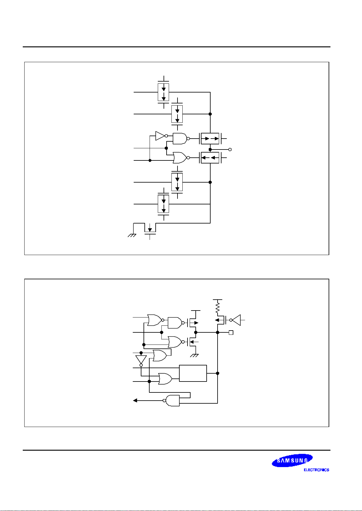
PIN CIRCUITS
V
DD
Pull-up
Enable
IN
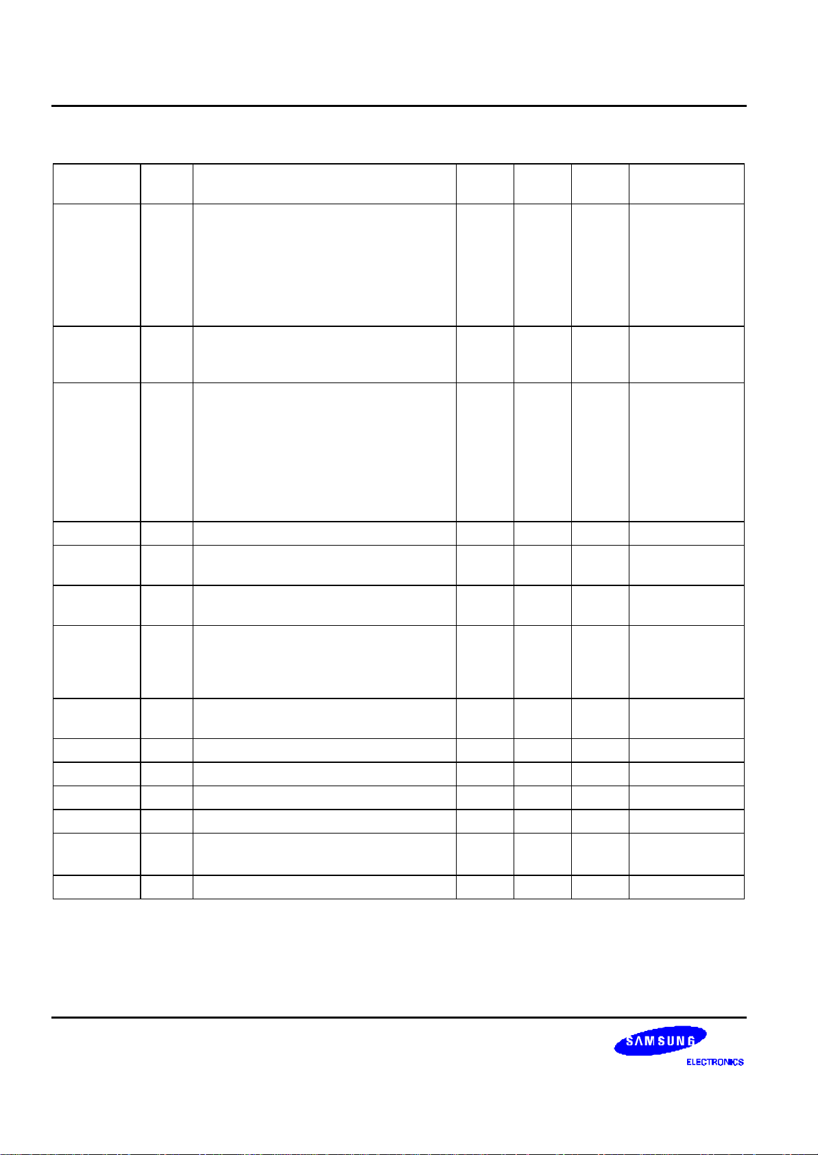
Figure 1-5. Pin Circuit Type B (RESET)
V
DD
Data
P-Channel
Out
Output
N-Channel
Disable
Ext.INT
Input
Normal
Data
Output
Pin Circuit
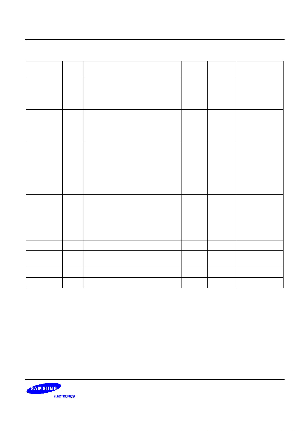
Type C
Disable
Figure 1-7. Pin Circuit Type D-2
V
V
DD
Data
Output
Disable
Pin Circuit
Type C
Noise
Filter
I/O
DD
Pull-up
Enable
I/O
Figure 1-6. Pin Circuit Type C
Figure 1-8. Pin Circuit Type D-4 (P3.5-P3.6)
1-11
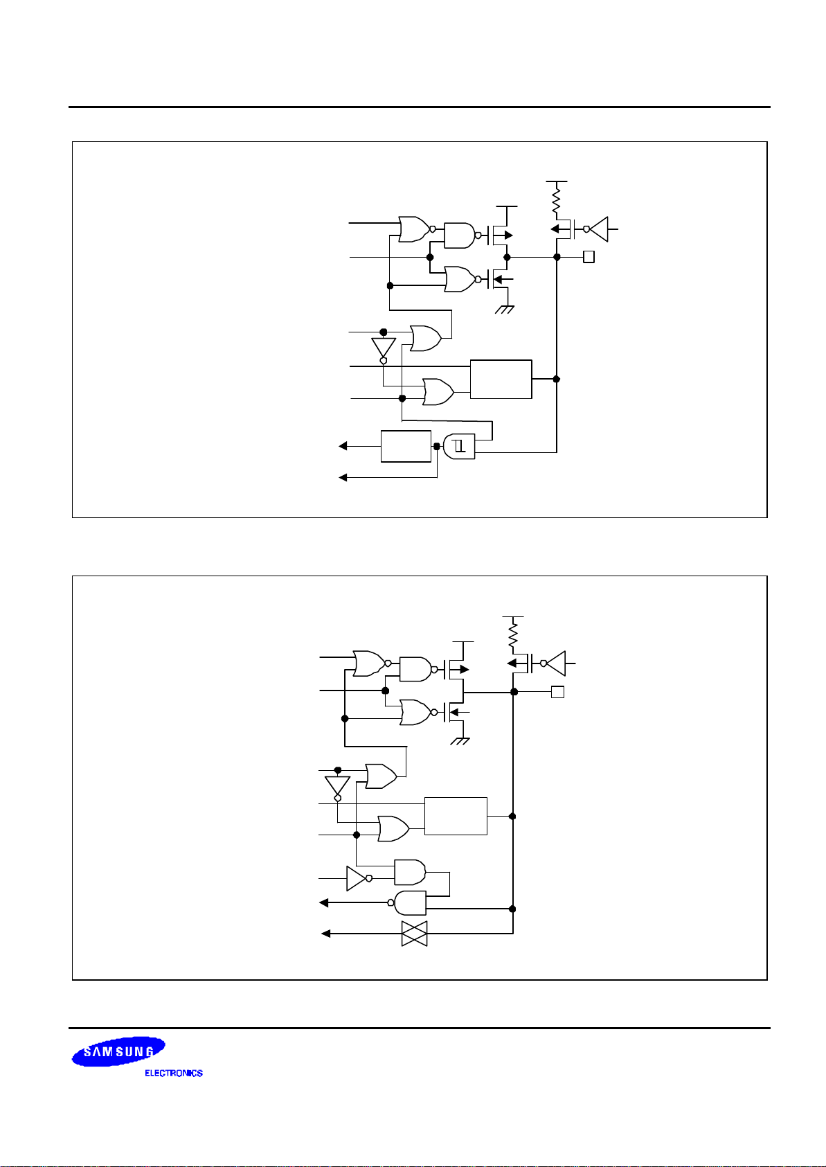
PRODUCT OVERVIEW S3C9484/C9488/F9488
VDD
VDD
P3.x Data
Alternative output
(TAOUT)
Output
M
U
X
Pin
Circuit
Pull-up
enable
I/O
Type C
Disable
Ext.INT
Noise
Filter
Normal Input
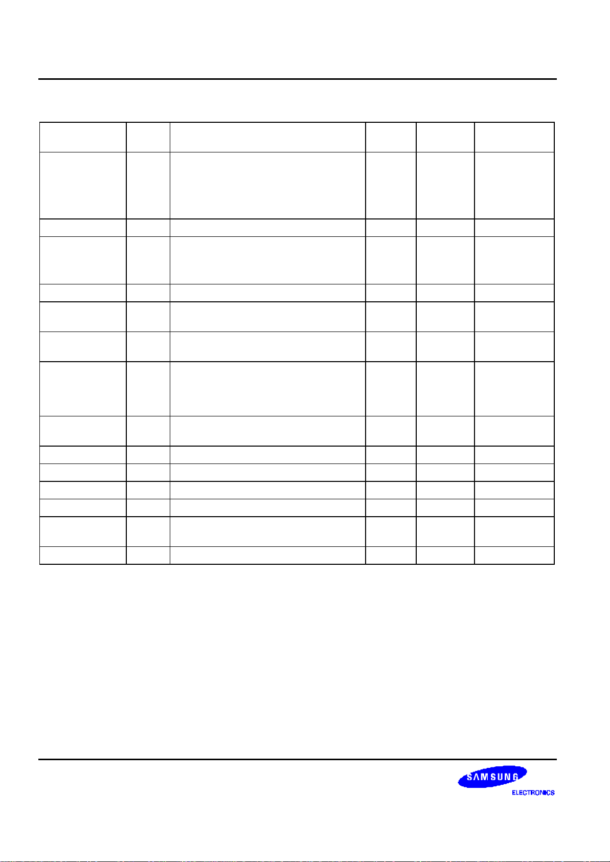
Figure 1-9. Pin Circuit Type D-5 (P3.4)
Output Data
Output Disable
(Input Mode)
Digital Input
Alternative I/O Enable
XTin,XTout
oscillation circuit
V
DD
V
DD
P-CH
N-CH
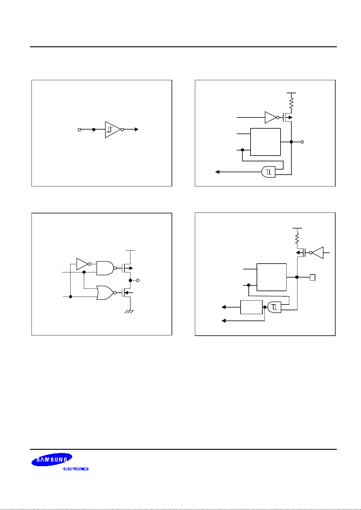
Figure 1-10. Pin Circuit Type E (P0.0, P0.1)
Pull-up
enable
MUX
Smart option
I/O
1-12
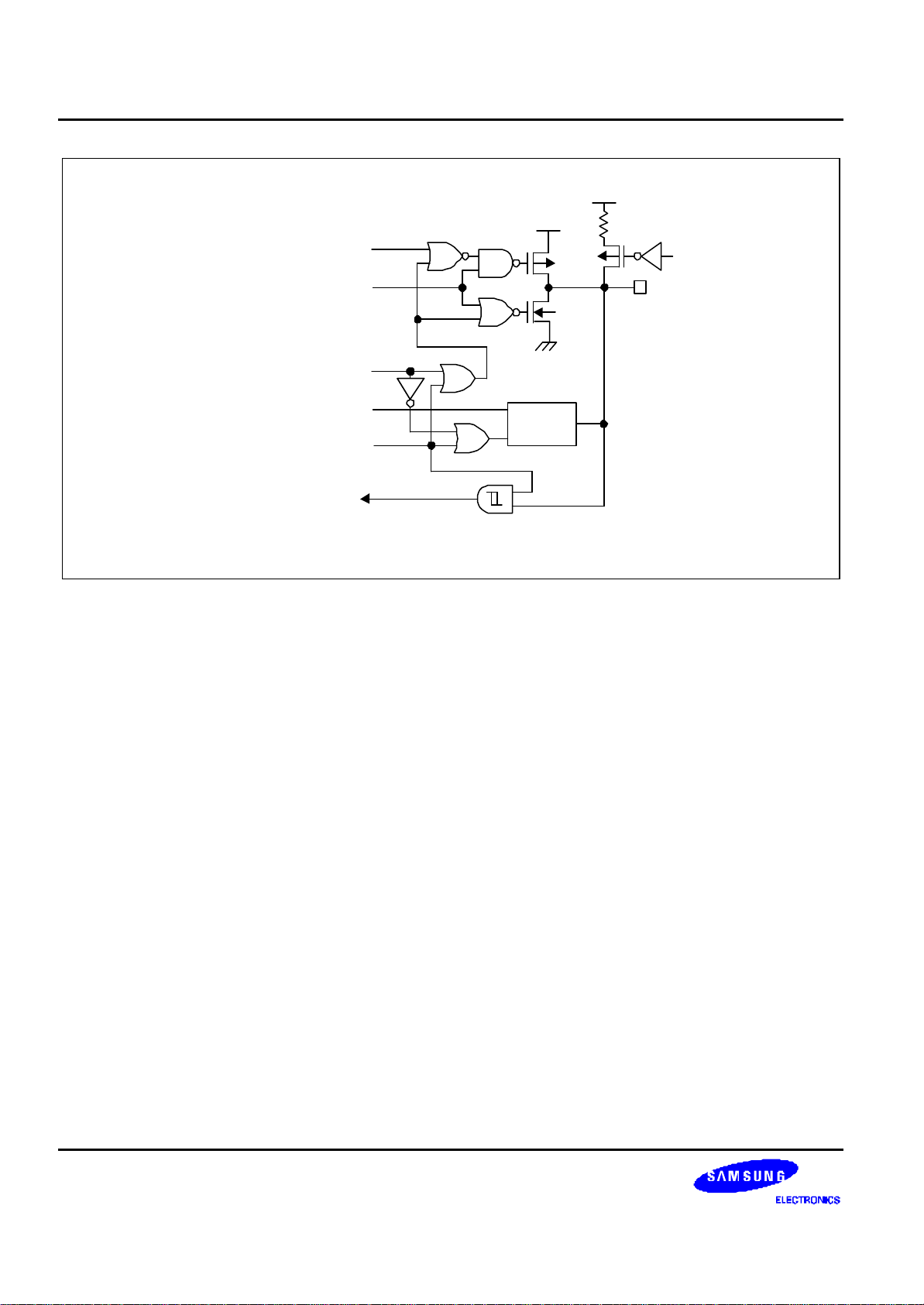
S3C9484/C9488/F9488 PRODUCT OVERVIEW
V
DD
Pull-up
Enable
Pull-up
enable
Data
Output
Circuit
Type C
I/O
Disable
ADC In EN
Data
to ADC
Figure 1-11. Pin Circuit Type E-1 (P0.3, P1.2–P1.3)
V
DD
Open-drain
V
DD
Smart option
Pull-up register
(50 kΩ typical)
Data
Output DIsable
(input mode)
Input Data
RESET
MUX
MUX
Figure 1-12. Pin Circuit Type E-2 (P0.2)
In/Out
1-13
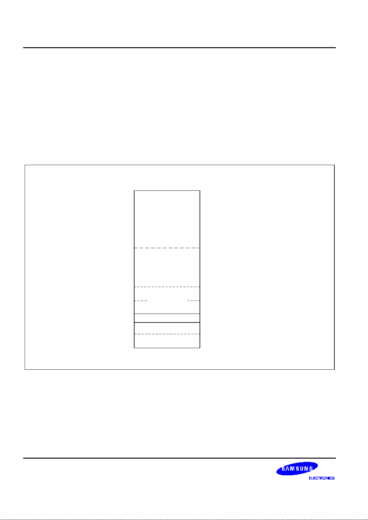
PRODUCT OVERVIEW S3C9484/C9488/F9488
V
DD
Pull-up
Enable
P1.0 -P1.1 Data
Buzzer Output
TB Underflow
Carrier on/off (P1.0)
Port Alternative option
M
U
X
Circuit
I/O
Type C
Output
Disable
ADC In EN
Data
to ADC
Figure 1-13. Pin Circuit Type E-3 (P1.0- P1.1)
1-14
S3C9484/C9488/F9488 PRODUCT OVERVIEW
V
LC4
V
LC3
SEG/COM
V
LC2
V
LC1
Figure 1-14. Pin Circuit Type H (SEG/COM)
Out
1-15
PRODUCT OVERVIEW S3C9484/C9488/F9488
V
LC4
V
LC3
SEG
Output
Disable
V
LC2
V
LC1
Open Drain EN
Data
Figure 1-15. Pin Circuit Type H-4
V
DD
V
DD
P-CH
Out
Pull-up
Enable
I/O
1-16
N-CH
LCD Out EN
SEG/COM
Output
Circuit
Type H
Disable
Input
Figure 1-16. Pin Circuit Type H-14 (P1.4-P1.7, P2, P3.0, P4.0-P4.6)
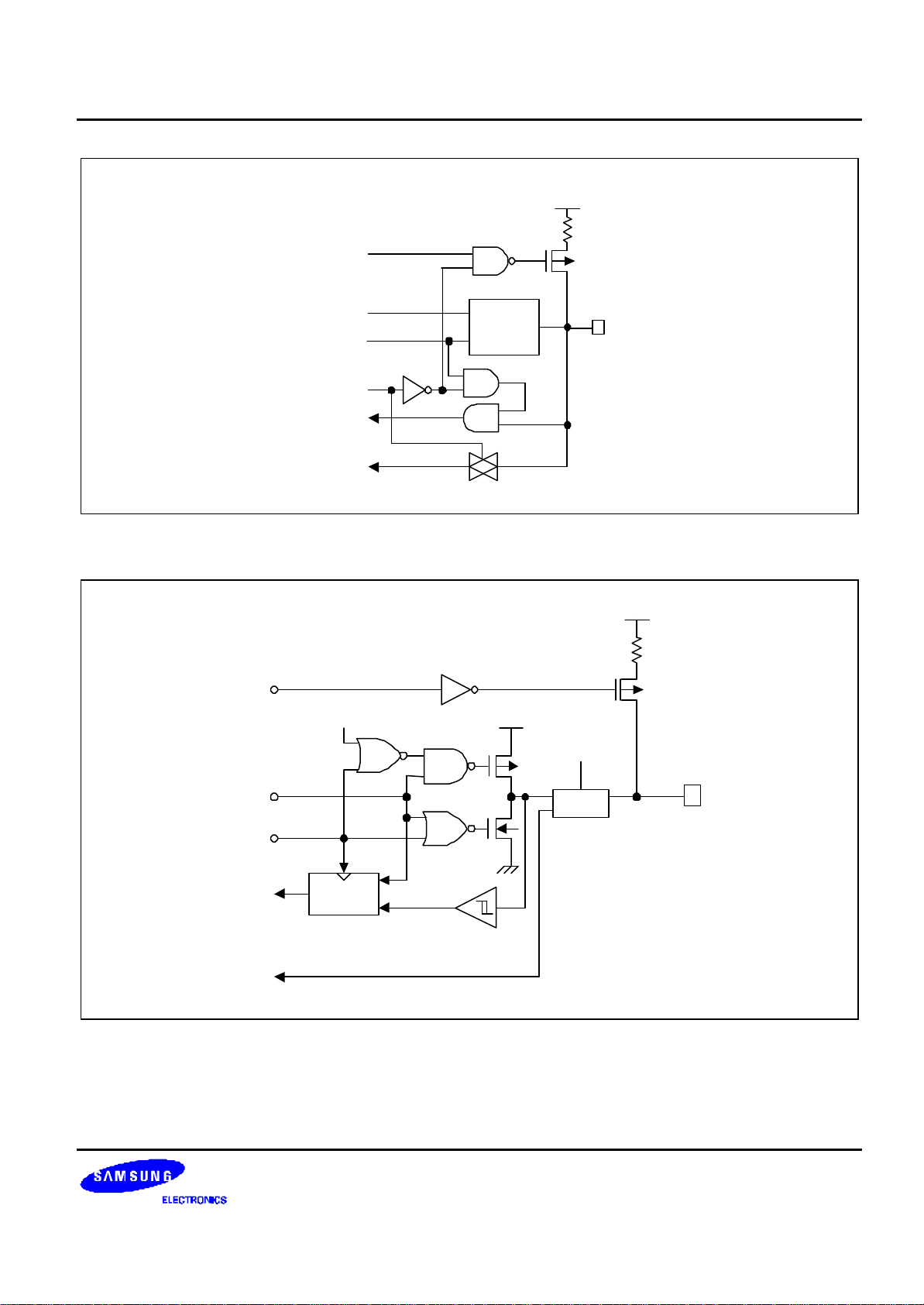
S3C9484/C9488/F9488 PRODUCT OVERVIEW
V
DD
V
DD
Open Drain EN
Data
LCD Out EN
SEG
Type H-4
Output Disable
Ext.INT
Noise
Filter
Normal Input
Figure 1-17. Pin Circuit Type H-15 (P3.3)
Circuit
V
P-CH
N-CH
DD
Pull-up
Enable
I/O
Open Drain EN
Data
LCD Out EN
COM
Output
Disable
ADC In EN
Normal In
ADC In
Figure 1-18. Pin Circuit Type H-16 (P0.4–P0.7)
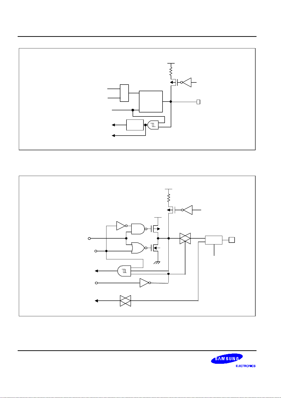
V
DD
Circuit
Type H-4
P-CH
N-CH
Pull-up
Enable
I/O
1-17
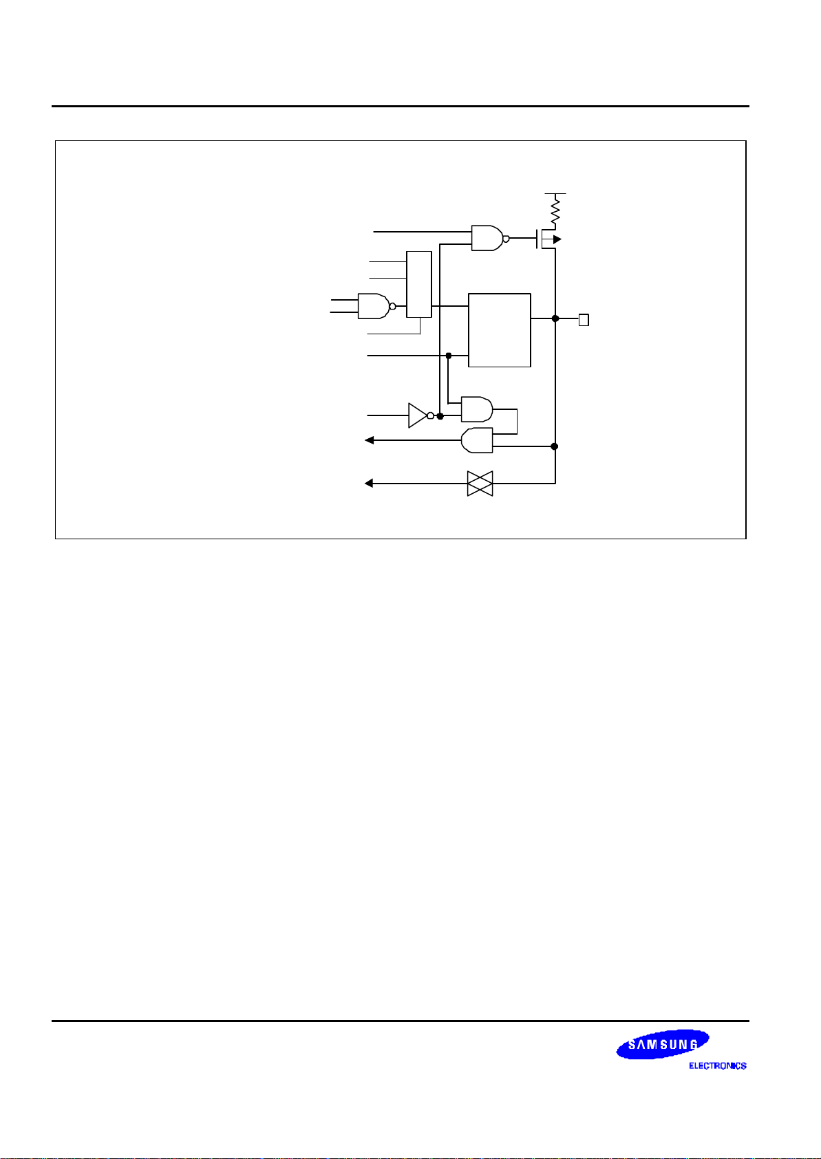
PRODUCT OVERVIEW S3C9484/C9488/F9488
V
DD
V
DD
Open Drain EN
P-CH
Data
N-CH
LCD Out EN
SEG
Circuit
Type H-4
Output Disable
Normal Input
Figure 1-19. Pin Circuit Type H-17 (P3.1-P3.2)
Pull-up
Enable
I/O
1-18

S3C9484/C9488/F9488 ADDRESS SPACES
2 ADDRESS SPACES
OVERVIEW
The S3C9484/C9488/F9488 microcontroller has two kinds of address space:
— Internal program memory (ROM)
— Internal register file
A 13-bit address bus supports program memory operations. A separate 8-bit register bus carries addresses and
data between the CPU and the internal register file.
The S3F9488 have 8-Kbytes of on-chip program memory, which is configured as the Internal ROM mode, all of the 8Kbyte internal program memory is used.
The S3C9484/C9488/F9488 microcontroller has 208 general-purpose registers in its internal register file. 47 bytes in
the register file are mapped for system and peripheral control functions. And 19 bytes in the page1 is mapped for
LCD display data area.
2-1
ADDRESS SPACES S3C9484/C9488/F9488
PROGRAM MEMORY (ROM)
Program memory (ROM) stores program codes or table data. The S3C9484/C9488 has 4K and 8Kbytes of internal
mask programmable program memory. The program memory address range is therefore 0H–0FFFH and 0H-1FFFH.
The S3F9488 have 8Kbytes (locations 0H–1FFFH) of internal multi time programmable (MTP) program memory (see
Figure 2-1).
The first 2-bytes of the ROM (0000H–0001H) are interrupt vector address.
Unused locations (0002H–00FFH except 3CH, 3DH, 3EH, 3FH) can be used as normal program memory.
The location 3CH, 3DH, 3EH, and 3FH is used as smart option ROM cell.
The program reset address in the ROM is 0100H.
(Decimal) (HEX)
8,191
8Kbyte
Program
Memory
Area
1FFFH
(S3C9488/F9488)
4,095
4Kbyte
Program
Memory
Area
Program Start
Smart option ROM cell
Interrupt Vector Area
0
1000H
0FFFH
(S3C9484)
0200H
0100H
003FH
003CH
0002H
0000H
Figure 2-1. Program Memory Address Space
2-2
S3C9484/C9488/F9488 ADDRESS SPACES
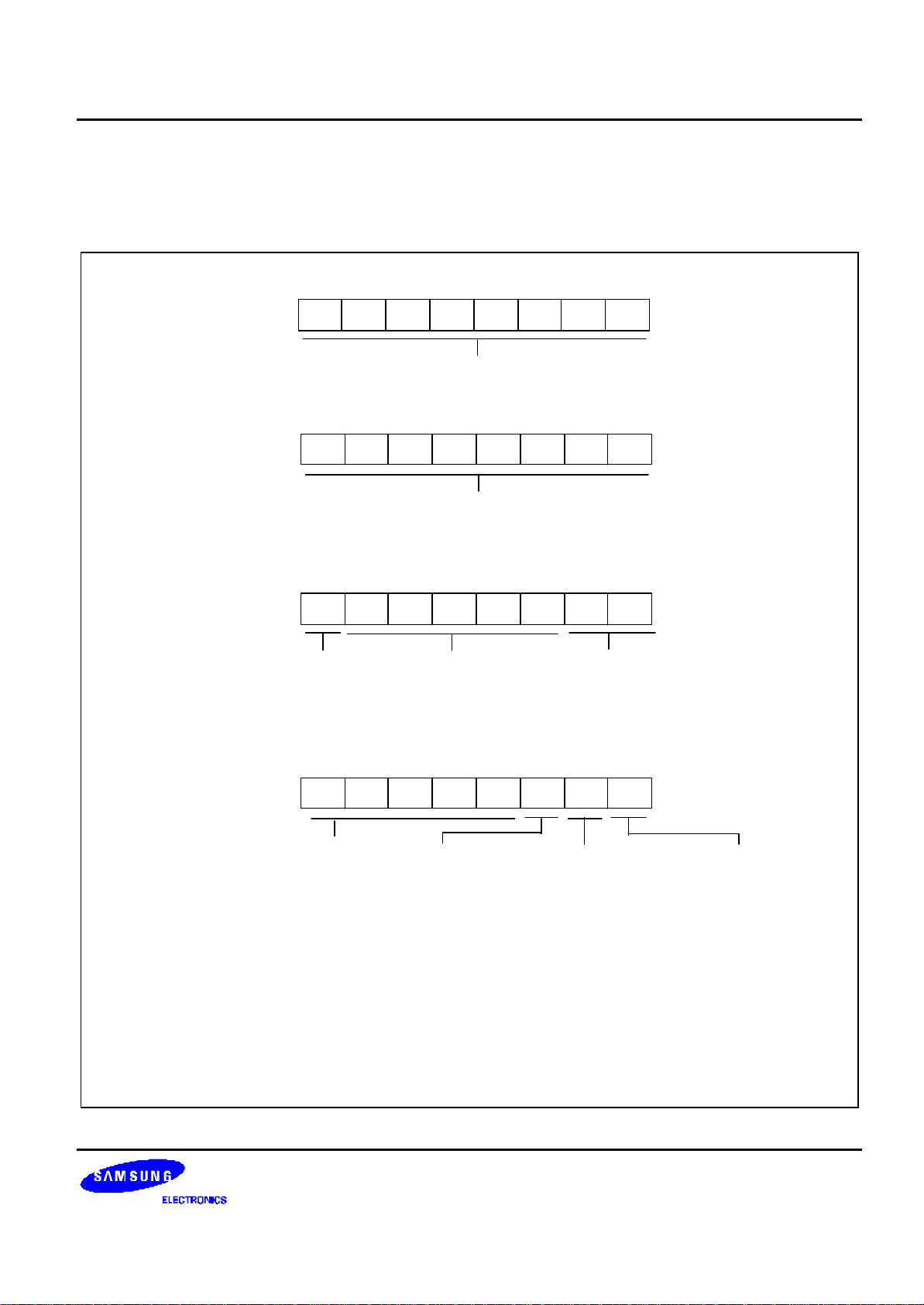
Smart Option
Smart option is the ROM option for starting condition of the chip. The ROM addresses used by smart option are from
003CH to 003FH. The default value of ROM is FFH.
ROM Address: 003CH
.7 .6 .5 .4 .3 .2 .1 .0MSB LSB
Not used
ROM Address: 003DH
.7 .6 .5 .4 .3 .2 .1 .0MSB LSB
P3CONH.7 -.0
The reset value of P3CONH (Port 3 Control Register High byte)
register is determined by 3DH.7-3DH.0 bits when CPU is reset.
ROM Address: 003EH
.7 .6 .5 .4 .3 .2 .1 .0MSB LSB
LVR enable
or disable bit:
0 = Disable
1 = Enable
.7 .6 .5 .4 .3 .2 .1 .0MSB LSB
Not used
NOTES:
1. The smart option value of 3DH determine P3.3-P3.6 initial port mode when cpu is reset.
The value of smart option is the same as normal setting value. You can refer to user manual chapter "9. I/O PORT".
2. The unused bits of 3CH, 3EH, 3FH must be logic "1".
3. When LVR is enabled, LVR level must be set to appropriate value, not default value.
4. You must determine P0.0-P0.2 function on smart option.
In other words, After reset operation, you cann't change P0.0-P0.2 function.
For a example, if you select xtin(P0.0)/xtout(P0.1) function by smart option, you cann't change on Normal I/O after
reset operation. Equally, RESETB(P0.2) pin function is the same.
P0.0/XTin, P0.1/XTout
pin function selection bit:
0 = XTin/Xtout pin enable
1 = Normal I/O pin enable
LVR level selection bits:
10100 = 2.6 V
01110 = 3.3 V
01011 = 3.9 V
ROM Address: 003FH
Not used
Watchdog timer
oscillator select bit:
0 = Internal RC
oscillator used
1 = Basic Timer
overflow used
P0.2/RESETB pin
selection bit:
0 = Nomal I/O P0.2
pin enable
1 = RESETB
Pin enable
Figure 2-2. Smart Option
2-3
ADDRESS SPACES S3C9484/C9488/F9488
REGISTER ARCHITECTURE
The upper 64-bytes of the S3C9484/C9488/F9488's internal register file are addressed as working registers, system
control registers and peripheral control registers. The lower 192-bytes of internal register file (00H–BFH) is called the
general-purpose register space. 274 registers in this space can be accessed; 208 are available for general-purpose
use. And 19 are available for LCD display register. But if LCD driver not used, available for general-purpose use.
For many SAM88RCRI microcontrollers, the addressable area of the internal register file is further expanded by
additional register pages at space of the general purpose register (00H–BFH). This register file expansion is not
implemented in the S3C9484/C9488/F9488, however.
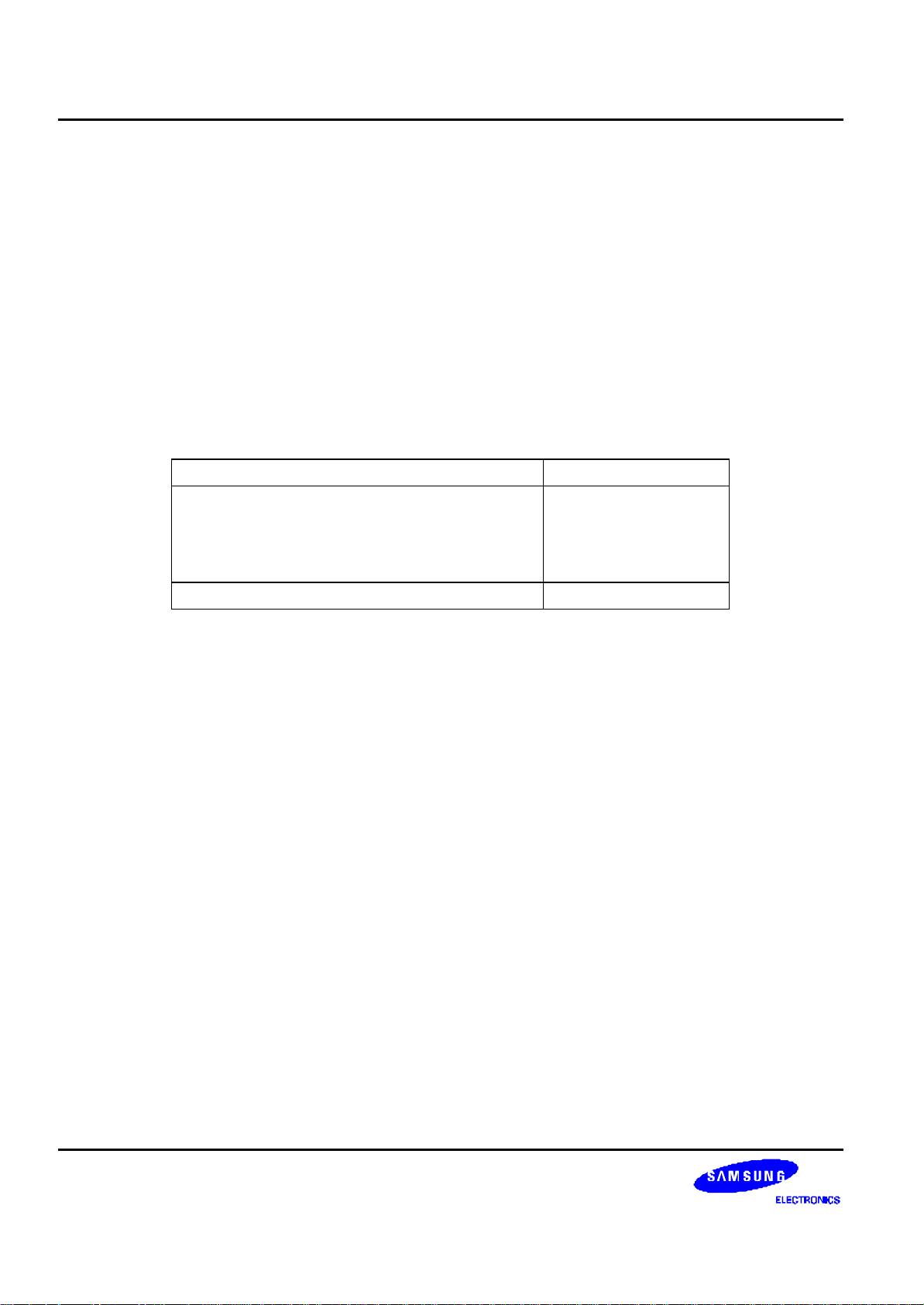
The specific register types and the area (in bytes) that they occupy in the internal register file are summarized in
Table 2-1.
Table 2-1. Register Type Summary
Register Type Number of Bytes
System and peripheral registers (page0 & page1) 47
General-purpose registers (including the 16-bit
common working register area)
LCD display Registers (page1) 19
208
Total Addressable Bytes 274
2-4
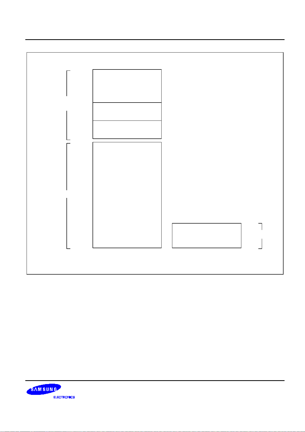
S3C9484/C9488/F9488 ADDRESS SPACES
FFH
Peripheral Control
Registers
64 Bytes of
Common Area
192 Bytes
E0H
DFH
D0H
CFH
C0H
BFH
00H
System Control
Registers
Working Registers
General Purpose
Register File
and Stack Area
~
Page 0
LCD Display Registers
&
Peripheral Register
Page 1
15H
22 Bytes
00H
Figure 2-3. Internal Register File Organization
2-5
ADDRESS SPACES S3C9484/C9488/F9488
COMMON WORKING REGISTER AREA (C0H–CFH)
The SAM88RCRI register architecture provides an efficient method of working register addressing that takes full
advantage of shorter instruction formats to reduce execution time.
This 16-byte address range is called common area. That is, locations in this area can be used as working registers
by operations that address any location on any page in the register file.
Registers are addressed either as a single 8-bit register or as a paired 16-bit register. In 16-bit register pairs, the
address of the first 8-bit register is always an even number and the address of the next register is an odd number.
The most significant byte of the 16-bit data is always stored in the even-numbered register; the least significant byte
is always stored in the next (+ 1) odd-numbered register.
MSB
Rn
LSB
Rn+1
n = Even address
Figure 2-4. 16-Bit Register Pairs
2-6
S3C9484/C9488/F9488 ADDRESS SPACES
SYSTEM STACK
S3F9-series microcontrollers use the system stack for subroutine calls and returns and to store data. The PUSH
and POP instructions are used to control system stack operations. The S3C9484/C9488/F9488 architecture
supports stack operations in the internal register file.
Stack Operations
Return addresses for procedure calls and interrupts and data are stored on the stack. The contents of the PC are
saved to stack by a CALL instruction and restored by the RET instruction. When an interrupt occurs, the contents of
the PC and the FLAGS registers are pushed to the stack. The IRET instruction then pops these values back to their
original locations. The stack address always decrements before a push operation and increments after a pop
operation. The stack pointer (SP) always points to the stack frame stored on the top of the stack, as shown in
Figure 2-5.
High Address
PCL
PCL
Top of
stack
PCH
Stack contents
after a call
instruction
Top of
stack
Low Address
PCH
Flags
Stack contents
after an
interrupt
Figure 2-5. Stack Operations
Stack Pointer (SP)
Register location D9H contains the 8-bit stack pointer (SP) that is used for system stack operations. After a reset,
the SP value is undetermined.
Because only internal memory space is implemented in the S3C9484/C9488/F9488, the SP must be initialized to an
8-bit value in the range 00H–0C0H.
NOTE
In case a Stack Pointer is initialized to 00H, it is decreased to FFH when stack operation starts. This
means that a Stack Pointer access invalid stack area. We recommend that a stack pointer is initialized to
C0H to set upper address of stack to BFH.
2-7

ADDRESS SPACES S3C9484/C9488/F9488
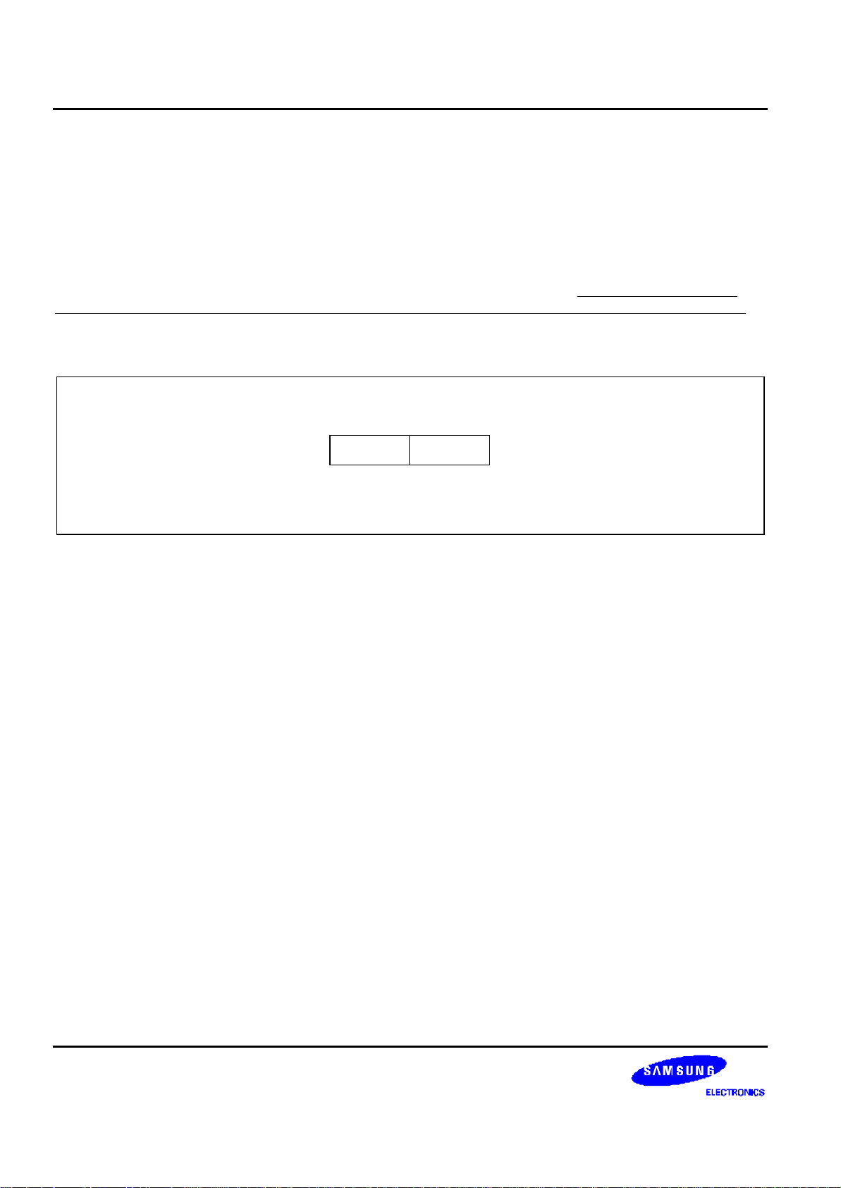
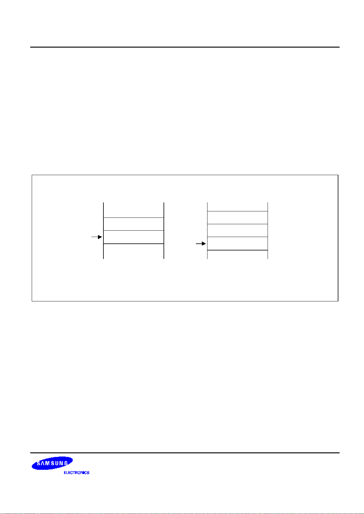
+ PROGRAMMING TIP — Standard Stack Operations Using PUSH and POP
The following example shows you how to perform stack operations in the internal register file using PUSH and POP
instructions:
LD SP,#0C0H ; SP ← C0H (Normally, the SP is set to C0H by the
; initialization routine)
•
•
•
PUSH SYM ; Stack address 0BFH ← SYM
PUSH R15 ; Stack address 0BEH ← R15
PUSH 20H ; Stack address 0BDH ← 20H
PUSH R3 ; Stack address 0BCH ← R3
•
•
•
POP R3 ; R3 ← Stack address 0BCH
POP 20H ; 20H ← Stack address 0BDH
POP R15 ; R15 ← Stack address 0BEH
POP SYM ; SYM ← Stack address 0BFH
2-8

S3C9484/C9488/F9488 ADDRESSING MODES
3 ADDRESSING MODES
OVERVIEW
Instructions that are stored in program memory are fetched for execution using the program counter. Instructions
indicate the operation to be performed and the data to be operated on. Addressing mode is the method used to
determine the location of the data operand. The operands specified in SAM88RC instructions may be condition
codes, immediate data, or a location in the register file, program memory, or data memory.
The S3C-series instruction set supports seven explicit addressing modes. Not all of these addressing modes are
available for each instruction. The seven addressing modes and their symbols are:
— Register (R)
— Indirect Register (IR)
— Indexed (X)
— Direct Address (DA)
— Indirect Address (IA)
— Relative Address (RA)
— Immediate (IM)
3-1

ADDRESSING MODES S3C9484/C9488/F9488
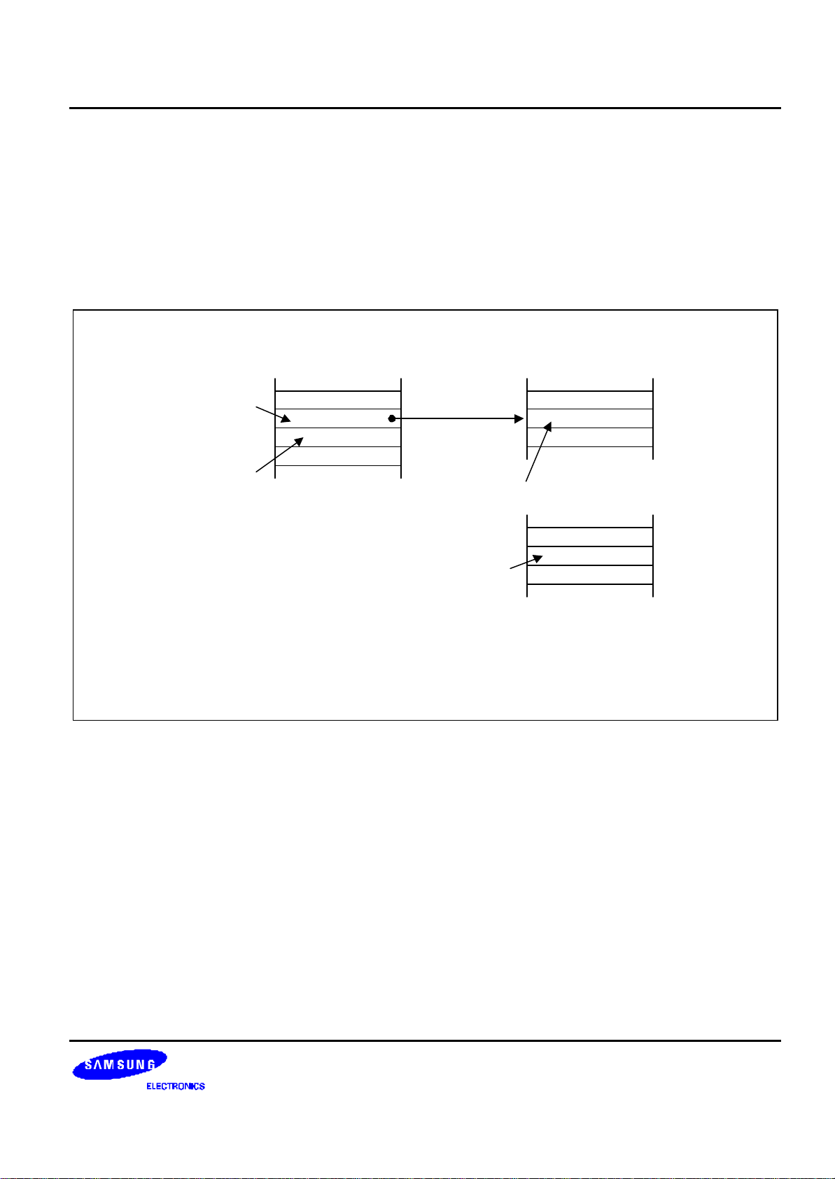
REGISTER ADDRESSING MODE (R)
In Register addressing mode (R), the operand value is the content of a specified register or register pair
(see Figure 3-1).
Working register addressing differs from Register addressing in that it uses a register pointer to specify an 8-byte
working register space in the register file and an 8-bit register within that space (see Figure 3-2).
Program Memory Register File
8-bit Register
File Address
One-Operand
Instruction
(Example)
Sample Instruction:
dst
OPCODE
Point to One
Register in Register
File
Value used in
Instruction Execution
OPERAND
DEC CNTR ; Where CNTR is the label of an 8-bit register address
4-bit
Working Register
Two-Operand
Instruction
(Example)
Sample Instruction:
Figure 3-1. Register Addressing
Program Memory
dst
src
OPCODE
MSB Point to
RP0 ot RP1
3 LSBs
Point to the
Working Register
(1 of 8)
Register File
RP0 or RP1
Selected
RP points
to start
of working
register
block
OPERAND
3-2
ADD R1, R2 ; Where R1 and R2 are registers in the currently
selected working register area.
Figure 3-2. Working Register Addressing
S3C9484/C9488/F9488 ADDRESSING MODES
INDIRECT REGISTER ADDRESSING MODE (IR)
In Indirect Register (IR) addressing mode, the content of the specified register or register pair is the address of the
operand. Depending on the instruction used, the actual address may point to a register in the register file, to program
memory (ROM), or to an external memory space (see Figures 3-3 through 3-6).
You can use any 8-bit register to indirectly address another register. Any 16-bit register pair can be used to indirectly
address another memory location.
Program Memory Register File
8-bit Register
File Address
One-Operand
Instruction
(Example)
dst
OPCODE
Point to One
ADDRESS
Register in Register
File
Address of Operand
used by Instruction
Value used in
Instruction Execution
Sample Instruction:
RL @SHIFT ; Where SHIFT is the label of an 8-bit register address
OPERAND
Figure 3-3. Indirect Register Addressing to Register File
3-3
 Loading...