


S3C84BB/F84BB
8-BIT CMOS
MICROCONTROLLERS
USER'S MANUAL
Revision 1

Important Notice
information in this publication has been carefully
checked and is believed to be entirely accurate at
the time of publication. Samsung assumes no
responsibility, however, for possible errors or
omissions, or for any consequences resulting from
the use of the information contained herein.
Samsung reserves the right to make changes in its
products or product specifications with the intent to
improve function or design at any time and without
notice and is not required to update this
documentation to reflect such changes.
This publication does not convey to a purchaser of
semiconductor devices described herein any license
under the patent rights of Samsung or others.
Samsung makes no warranty, representation, or
guarantee regarding the suitability of its products for
any particular purpose, nor does Samsung assume
any liability arising out of the application or use of
any product or circuit and specifically disclaims any
and all liability, including without limitation any
consequential or incidental damages.
S3C84BB/F84BB 8-Bit CMOS Microcontrollers
User's Manual, Revision 1
Publication Number: 20-S3-C84BB/F84BB-0800
"Typical" parameters can and do vary in different
applications. All operating parameters, including
"Typicals" must be validated for each customer
application by the customer's technical experts.
Samsung products are not designed, intended, or
authorized for use as components in systems
intended for surgical implant into the body, for other
applications intended to support or sustain life, or for
any other application in which the failure of the
Samsung product could create a situation where
personal injury or death may occur.
Should the Buyer purchase or use a Samsung
product for any such unintended or unauthorized
application, the Buyer shall indemnify and hold
Samsung and its officers, employees, subsidiaries,
affiliates, and distributors harmless against all
claims, costs, damages, expenses, and reasonable
attorney fees arising out of, either directly or
indirectly, any claim of personal injury or death that
may be associated with such unintended or
unauthorized use, even if such claim alleges that
Samsung was negligent regarding the design or
manufacture of said product.
© 2000 Samsung Electronics
All rights reserved. No part of this publication may be reproduced, stored in a retrieval system, or transmitted in
any form or by any means, electric or mechanical, by photocopying, recording, or otherwise, without the prior
written consent of Samsung Electronics.
Samsung Electronics' microcontroller business has been awarded full ISO-14001
certification (BSI Certificate No. FM24653). All semiconductor products are
designed and manufactured in accordance with the highest quality standards and
objectives.
Samsung Electronics Co., Ltd.
San #24 Nongseo-Ri, Kiheung- Eup
Yongin-City, Kyunggi-Do, Korea
C.P.O. Box #37, Suwon 449-900
TEL: (82)-(31)-209-1907
FAX: (82)-(31)-209-1899
Home Page: http://www.intl.samsungsemi.com
Printed in the Republic of Korea

Preface
The S3C84BB/F84BB Microcontroller User's Manual is designed for application designers and programmers who
are using the S3C84BB/84BB microcontroller for application development.
It is organized in two main parts:
Part I Programming Model Part II Hardware Descriptions
Part I contains software-related information to familiarize you with the microcontroller's architecture, programming
model, instruction set, and interrupt structure. It has six chapters:
Chapter 1 Product Overview
Chapter 2 Address Spaces
Chapter 3 Addressing Modes
Chapter 1, "Product Overview," is a high-level introduction to S3C84BB/F84BB with general product descriptions,
as well as detailed information about individual pin characteristics and pin circuit types.
Chapter 2, "Address Spaces," describes program and data memory spaces, the internal register file, and register
addressing. Chapter 2 also describes working register addressing, as well as system stack and user-defined
stack operations.
Chapter 3, "Addressing Modes," contains detailed descriptions of the addressing modes that are supported by the
S3C8-series CPU.
Chapter 4 Control Registers
Chapter 5 Interrupt Structure
Chapter 6 Instruction Set
Chapter 4, "Control Registers," contains overview tables for all mapped system and peripheral control register
values, as well as detailed one-page descriptions in a standardized format. You can use these easy-to-read,
alphabetically organized, register descriptions as a quick-reference source when writing programs.
Chapter 5, "Interrupt Structure," describes the S3C84BB/F84BB interrupt structure in detail and further prepares
you for additional information presented in the individual hardware module descriptions in Part II.
Chapter 6, "Instruction Set," describes the features and conventions of the instruction set used for all S3C8-series
microcontrollers. Several summary tables are presented for orientation and reference. Detailed descriptions of
each instruction are presented in a standard format. Each instruction description includes one or more practical
examples of how to use the instruction when writing an application program.
A basic familiarity with the information in Part I will help you to understand the hardware module descriptions in
Part II. If you are not yet familiar with the S3C-series microcontroller family and are reading this manual for the
first time, we recommend that you first read Chapters 1–3 carefully. Then, briefly look over the detailed
information in Chapters 4, 5, and 6. Later, you can reference the information in Part I as necessary.
Part II "hardware Descriptions," has detailed information about specific hardware components of the
S3C84BB/F84BB microcontroller. Also included in Part II are electrical, mechanical, Flash MCU, and development
tools data. It has 15 chapters:
Chapter 7 Clock Circuit
Chapter 8 RESET and Power-Down
Chapter 9 I/O Ports
Chapter 10 Basic Timer
Chapter 11 8-bit Timer A/B/C(0/1)
Chapter 12 16-bit Timer 1(0/1)
Chapter 13 Serial I/O Port
Chapter 14 UART(0/1)
Two order forms are included at the back of this manual to facilitate customer order for S3C84BB/F84BB
microcontrollers: the Mask ROM Order Form, and the Mask Option Selection Form. You can photocopy these
forms, fill them out, and then forward them to your local Samsung Sales Representative.
Chapter 15 10-bit A/D Converter
Chapter 16 8-bit D/A Converter
Chapter 17 Pattern Generation Module
Chapter 18 Embedded Flash Memory Interface
Chapter 19 Electrical Data
Chapter 20 Mechanical Data
Chapter 21 Development Tools
S3C84BB/F84BB MICROCONTROLLER iii


Table of Contents
Part I — Programming Model
Chapter 1 Product Overview
S3C8-Series Microcontrollers .......................................................................................................................1-1
S3C84BB/F84BB Microcontroller..................................................................................................................1-1
Features ........................................................................................................................................................1-2
Block Diagram ...............................................................................................................................................1-3
Pin Assignment .............................................................................................................................................1-4
Pin Descriptions ............................................................................................................................................1-6
Pin Circuits ....................................................................................................................................................1-9
Chapter 2 Address Spaces
Overview........................................................................................................................................................2-1
Program Memory (ROM)...............................................................................................................................2-2
Register Architecture.....................................................................................................................................2-3
Register Page Pointer (PP) ..................................................................................................................2-5
Register Set 1 .......................................................................................................................................2-6
Register Set 2 .......................................................................................................................................2-6
Prime Register Space...........................................................................................................................2-7
Working Registers ................................................................................................................................2-8
Using The Register Pointers.................................................................................................................2-9
Register Addressing ......................................................................................................................................2-11
Common Working Register Area (C0H–CFH) .....................................................................................2-13
4-Bit Working Register Addressing ......................................................................................................2-14
8-Bit Working Register Addressing ......................................................................................................2-16
System And User Stack ................................................................................................................................2-18
Chapter 3 Addressing Modes
Overview........................................................................................................................................................3-1
Register Addressing Mode (R)......................................................................................................................3-2
Indirect Register Addressing Mode (IR)........................................................................................................3-3
Indexed Addressing Mode (X).......................................................................................................................3-7
Direct Address Mode (DA) ............................................................................................................................3-10
Indirect Address Mode (IA) ...........................................................................................................................3-12
Relative Address Mode (RA).........................................................................................................................3-13
Immediate Mode (IM) ....................................................................................................................................3-14
S3C84BB/F84BB MICROCONTROLLER v

Table of Contents (Continued)
Chapter 4 Control Registers
Overview .............................................................................................................................................. 4-1
Chapter 5 Interrupt Structure
Overview....................................................................................................................................................... 5-1
Interrupt Types..................................................................................................................................... 5-2
S3C84BB/F84BB Interrupt Structure ................................................................................................... 5-3
Interrupt Vector Addresses .................................................................................................................. 5-5
Enable/Disable Interrupt Instructions (EI, DI) ...................................................................................... 5-7
System-Level Interrupt Control Registers............................................................................................ 5-7
Interrupt Processing Control Points ..................................................................................................... 5-8
Peripheral Interrupt Control Registers ................................................................................................. 5-9
System Mode Register (SYM) ............................................................................................................. 5-10
Interrupt Mask Register (IMR) ............................................................................................................. 5-11
Interrupt Priority Register (IPR)............................................................................................................ 5-12
Interrupt Request Register (IRQ)......................................................................................................... 5-14
Interrupt Pending Function Types........................................................................................................ 5-15
Interrupt Source Polling Sequence ...................................................................................................... 5-16
Interrupt Service Routines ................................................................................................................... 5-16
Generating Interrupt Vector Addresses ............................................................................................... 5-17
Nesting of Vectored Interrupts ............................................................................................................. 5-17
Chapter 6 Instruction Set
Overview....................................................................................................................................................... 6-1
Data Types........................................................................................................................................... 6-1
Register Addressing............................................................................................................................. 6-1
Addressing Modes ............................................................................................................................... 6-1
Flags Register (FLAGS)....................................................................................................................... 6-6
Flag Descriptions ................................................................................................................................. 6-7
Instruction Set Notation........................................................................................................................ 6-8
Condition Codes .................................................................................................................................. 6-12
Instruction Descriptions........................................................................................................................ 6-13
vi S3C84BB/F84BB MICROCONTROLLER

Table of Contents (Continued)
Part II Hardware Descriptions
Chapter 7 Clock Circuit
Overview........................................................................................................................................................7-1
System Clock Circuit ............................................................................................................................7-1
Clock Status During Power-Down Modes ............................................................................................7-2
System Clock Control Register (CLKCON) ..........................................................................................7-3
Chapter 8 RESET and Power-Down
System Reset ................................................................................................................................................8-1
Overview...............................................................................................................................................8-1
Normal Mode Reset Operation.............................................................................................................8-1
Hardware Reset Values........................................................................................................................8-2
Power-Down Modes ......................................................................................................................................8-5
Stop Mode ............................................................................................................................................8-5
Idle Mode ..............................................................................................................................................8-6
Chapter 9 I/O Ports
Overview........................................................................................................................................................9-1
Port Data Registers ..............................................................................................................................9-2
Port 0 ....................................................................................................................................................9-3
Port 1 ....................................................................................................................................................9-5
Port 2 ....................................................................................................................................................9-7
Port 3 ....................................................................................................................................................9-10
Port 4 ....................................................................................................................................................9-13
Port 5 ....................................................................................................................................................9-17
Port 6 ....................................................................................................................................................9-20
Port 7 ....................................................................................................................................................9-21
Port 8 ....................................................................................................................................................9-23
Chapter 10 Basic Timer
Overview........................................................................................................................................................10-1
Basic Timer (BT)...................................................................................................................................10-1
Basic Timer Control Register (BTCON) ...............................................................................................10-1
Basic Timer Function Description.........................................................................................................10-3
S3C84BB/F84BB MICROCONTROLLER vii

Table of Contents (Continued)
Chapter 11 8-bit Timer A/B/C(0/1)
8-Bit Timer A................................................................................................................................................. 11-1
Overview .............................................................................................................................................. 11-1
Function Description ............................................................................................................................ 11-2
Timer A Control Register (TACON) ..................................................................................................... 11-3
Block Diagram...................................................................................................................................... 11-4
8-Bit Timer B................................................................................................................................................. 11-5
Overview .............................................................................................................................................. 11-5
Block Diagram...................................................................................................................................... 11-5
Timer B Control Register (TBCON) ..................................................................................................... 11-6
Timer B Pulse Width Calculations ....................................................................................................... 11-7
8-Bit Timer C (0/1) ........................................................................................................................................ 11-11
Overview .............................................................................................................................................. 11-11
Timer C(0/1) Control Register (TCCON0, TCCON1) .......................................................................... 11-12
Block Diagram...................................................................................................................................... 11-13
Chapter 12 16-bit Timer 1(0/1)
Overview....................................................................................................................................................... 12-1
Function Description ............................................................................................................................ 12-2
Timer 1(0/1) Control Register (T1CON0, T1CON1) ............................................................................ 12-3
Block Diagram...................................................................................................................................... 12-6
Chapter 13 Serial I/O Port
Overview....................................................................................................................................................... 13-1
Programming Procedure...................................................................................................................... 13-1
SIO Control Register (SIOCON) .......................................................................................................... 13-2
SIO Prescaler Register (SIOPS).......................................................................................................... 13-3
Block Diagram...................................................................................................................................... 13-3
Serial I/O Timing Diagrams.................................................................................................................. 13-4
viii S3C84BB/F84BB MICROCONTROLLER

Table of Contents (Continued)
Chapter 14 UART(0/1)
Overview........................................................................................................................................................14-1
Programming Procedure ......................................................................................................................14-1
Uart Control Register (UARTCON0, UARTCON1) ..............................................................................14-2
Uart Interrupt Pending Register (UARTPND).......................................................................................14-3
Uart Data Register (UDATA0, UDATA1)..............................................................................................14-4
Uart Baud Rate Data Register (BRDATA0, BRDATA1).......................................................................14-4
Baud Rate Calculations ........................................................................................................................14-4
Block Diagram ...............................................................................................................................................14-6
Uart Mode 0 Function Description........................................................................................................14-7
Uart Mode 1 Function Description........................................................................................................14-8
Uart Mode 2 Function Description........................................................................................................14-9
Uart Mode 3 Function Description........................................................................................................14-10
Serial Communication for Multiprocessor Configurations ....................................................................14-11
Chapter 15 10-bit A/D Converter
Overview........................................................................................................................................................15-1
Function Description......................................................................................................................................15-1
Conversion Timing................................................................................................................................15-2
A/D Converter Control Register (ADACON).........................................................................................15-2
Internal Reference Voltage Levels .......................................................................................................15-4
Conversion Timing................................................................................................................................15-4
Internal A/D Conversion Procedure......................................................................................................15-5
Chapter 16 10-bit D/A Converter
Overview........................................................................................................................................................16-1
D/A Conversion Control Register (ADACON) ......................................................................................16-2
D/A Conversion Data Register (DADATA) ...........................................................................................16-2
Block Diagram ......................................................................................................................................16-3
Chapter 17 Pattern Generation Module
Overview........................................................................................................................................................17-1
Pattern Gneration Flow.........................................................................................................................17-1
S3C84BB/F84BB MICROCONTROLLER ix

Table of Contents (Continued)
Chapter 18 Embedded FLASH Memory Interface
Overview....................................................................................................................................................... 18-1
FLASH Memory Control Registers ............................................................................................................... 18-3
Sector Erase ................................................................................................................................................. 18-5
Programming ................................................................................................................................................ 18-9
Data Protection ............................................................................................................................................. 18-12
Chapter 19 Electrical Data
Overview .............................................................................................................................................. 19-1
Chapter 20 Mechanical Data
Overview .............................................................................................................................................. 20-1
Chapter 21 Development Tools
Overview....................................................................................................................................................... 21-1
Shine .................................................................................................................................................... 21-1
SAMA Assembler ................................................................................................................................. 21-1
SASM88 ............................................................................................................................................... 21-1
HEX2ROM ........................................................................................................................................... 21-1
Target Boards ...................................................................................................................................... 21-1
TB84BB Target Board.......................................................................................................................... 21-3
IDLE LED ............................................................................................................................................. 21-5
STOP LED ........................................................................................................................................... 21-5
x S3C84BB/F84BB MICROCONTROLLER

List of Figures
Figure Title Page
Number Number
1-1 S3C84BB/F84BB Block Diagram ...............................................................................1-3
1-2 S3C84BB/F84BB Pin Assignment (80-QFP)..............................................................1-4
1-3 S3C84BB/F84BB Pin Assignment (80-TQFP) ...........................................................1-5
1-4 Pin Circuit Type B (RESETB) ......................................................................................1-9
1-5 Pin Circuit Type C.......................................................................................................1-9
1-6 Pin Circuit Type D (P0, P1, P2 except P2.3, P3, P8 except P8.4, P8.5) ...................1-10
1-7 Pin Circuit Type D-1 (P4, P8.4, P8,5).........................................................................1-10
1-8 Pin Circuit Type D-2 (P2.3).........................................................................................1-11
1-9 Pin Circuit Type E (ADC0-ADC7)...............................................................................1-11
1-10 Pin Circuit Type F (P6) ...............................................................................................1-12
1-11 Pin Circuit Type G (P5.7-P5.4)...................................................................................1-12
2-1 Program Memory Address Space ..............................................................................2-2
2-2 Internal Register File Organization.............................................................................2-4
2-3 Register Page Pointer (PP) ........................................................................................2-5
2-4 Set 1, Set 2, Prime Area Register ..............................................................................2-7
2-5 8-Byte Working Register Areas (Slices) .....................................................................2-8
2-6 Contiguous 16-Byte Working Register Block .............................................................2-9
2-7 Non-Contiguous 16-Byte Working Register Block .....................................................2-10
2-8 16-Bit Register Pair ....................................................................................................2-11
2-9 Register File Addressing ............................................................................................2-12
2-10 Common Working Register Area................................................................................2-13
2-11 4-Bit Working Register Addressing ............................................................................2-15
2-12 4-Bit Working Register Addressing Example .............................................................2-15
2-13 8-Bit Working Register Addressing ............................................................................2-16
2-14 8-Bit Working Register Addressing Example .............................................................2-17
2-15 Stack Operations ........................................................................................................2-18
3-1 Register Addressing ...................................................................................................3-2
3-2 Working Register Addressing.....................................................................................3-2
3-3 Indirect Register Addressing to Register File.............................................................3-3
3-4 Indirect Register Addressing to Program Memory .....................................................3-4
3-5 Indirect Working Register Addressing to Register File ..............................................3-5
3-6 Indirect Working Register Addressing to Program or Data Memory ..........................3-6
3-7 Indexed Addressing to Register File ..........................................................................3-7
3-8 Indexed Addressing to Program or Data Memory with Short Offset ..........................3-8
3-9 Indexed Addressing to Program or Data Memory......................................................3-9
3-10 Direct Addressing for Load Instructions .....................................................................3-10
3-11 Direct Addressing for Call and Jump Instructions ......................................................3-11
3-12 Indirect Addressing.....................................................................................................3-12
3-13 Relative Addressing....................................................................................................3-13
3-14 Immediate Addressing................................................................................................3-14
S3C84BB/F84BB MICROCONTROLLER xi

List of Figures (Continued)
Figure Title Page
Number Number
4-1 Register Description Format ...................................................................................... 4-4
5-1 S3C8-Series Interrupt Types ..................................................................................... 5-2
5-2 S3C84BB/F84BB Interrupt Structure ......................................................................... 5-4
5-3 ROM Vector Address Area ........................................................................................ 5-5
5-4 Interrupt Function Diagram ........................................................................................ 5-8
5-5 System Mode Register (SYM) ................................................................................... 5-10
5-6 Interrupt Mask Register (IMR) ................................................................................... 5-11
5-7 Interrupt Request Priority Groups .............................................................................. 5-12
5-8 Interrupt Priority Register (IPR) ................................................................................. 5-13
5-9 Interrupt Request Register (IRQ)............................................................................... 5-14
6-1 System Flags Register (FLAGS) ............................................................................... 6-6
7-1 Main Oscillator Circuit (Crystal or Ceramic Oscillator) .............................................. 7-1
7-2 System Clock Circuit Diagram ................................................................................... 7-2
7-3 System Clock Control Register (CLKCON) ............................................................... 7-3
9-1 Port 0 Control Register (P0CON) .............................................................................. 9-4
9-2 Port 1 Control Register (P1CON) .............................................................................. 9-6
9-3 Port 2 High-Byte Control Register (P2CONH)........................................................... 9-8
9-4 Port 2 Low-Byte Control Register (P2CONL) ............................................................ 9-9
9-5 Port 3 High-Byte Control Register (P3CONH)........................................................... 9-11
9-6 Port 3 Low-Byte Control Register (P3CONL) ............................................................ 9-12
9-7 Port 4 High-Byte Control Register (P4CONH)........................................................... 9-14
9-8 Port 4 Low-Byte Control Register (P4CONL) ............................................................ 9-15
9-9 Port 4 Interrupt Control Register (P4INT) .................................................................. 9-16
9-10 Port 4 Interrupt Pending Register (P4INTPND)......................................................... 9-16
9-11 Port 5 High-Byte Control Register (P5CONH)........................................................... 9-18
9-12 Port 5 Low-Byte Control Register (P5CONL) ............................................................ 9-19
9-13 Port 7 Control Register (P7CON) .............................................................................. 9-22
9-14 Port 8 High-Byte Control Register (P8CONH)........................................................... 9-24
9-15 Port 8 Low-Byte Control Register (P8CONL) ............................................................ 9-25
9-16 Port 8 Interrupt Pending Register (P8INTPND)......................................................... 9-26
xii S3C84BB/F84BB MICROCONTROLLER

List of Figures (Continued)
Page Title Page
Number Number
10-1 Basic Timer Control Register (BTCON) .....................................................................10-2
10-2 Basic Timer Block Diagram ........................................................................................10-4
11-1 Timer A Control Register (TACON)............................................................................11-3
11-2 Timer A Functional Block Diagram.............................................................................11-4
11-3 Timer B Functional Block Diagram.............................................................................11-5
11-4 Timer B Control Register (TBCON)............................................................................11-6
11-5 Timer B Data Registers (TBDATAH, TBDATAL) .......................................................11-6
11-6 Timer B Output Flip-Flop Waveforms in Repeat Mode ..............................................11-8
11-7 Timer C(0/1) Control Register (TCCON0, TCCON1) .................................................11-12
11-8 Timer C(0/1) Functional Block Diagram .....................................................................11-13
12-1 Timer 1(0/1) Control Register (T1CON0, T1CON1)...................................................12-4
12-2 Timer A and Timer 1(0/1) Pending Register (TINTPND) ...........................................12-5
12-3 Timer 1(0/1) Functional Block Diagram......................................................................12-6
13-1 SIO Module Control Register (SIOCON)....................................................................13-2
13-2 SIO Prescaler Register (SIOPS) ................................................................................13-3
13-3 SIO Functional Block Diagram ...................................................................................13-3
13-4 SIO Timing in Transmit/Receive Mode (Tx at falling edge, SIOCON.4=0) ................13-4
13-5 SIO Timing in Transmit/Receive Mode (Tx at rising edge, SIOCON.4=1).................13-4
13-6 SIO Timing in Receive-Only Mode (Rising edge start) ..............................................13-5
14-1 UART Control Register (UARTCON0, UARTCON1) .................................................14-2
14-2 UART Interrupt Pending Register (UARTPND)..........................................................14-3
14-3 UART Data Register (UDATA0, UDATA1).................................................................14-4
14-4 UART Baud Rate Data Register (BRDATA0, BRDATA1)..........................................14-4
14-5 UART Functional Block Diagram................................................................................14-6
14-6 Timing Diagram for UART Mode 0 Operation ............................................................14-7
14-7 Timing Diagram for UART Mode 1 Operation ............................................................14-8
14-8 Timing Diagram for UART Mode 2 Operation ............................................................14-9
14-9 Timing Diagram for UART Mode 3 Operation ............................................................14-10
14-10 Connection Example for Multiprocessor Serial Data Communications .....................14-12
15-1 A/D Converter Control Register (ADACON)...............................................................15-2
15-2 A/D Converter Data Register (ADDATAH, ADDATAL) ..............................................15-3
15-3 A/D Converter Circuit Diagram...................................................................................15-3
15-4 A/D Converter Timing Diagram ..................................................................................15-4
15-5 Recommended A/D Converter Circuit Highest Absolute Accuracy............................15-5
16-1 D/A Converter Control Register (ADACON)...............................................................16-2
16-2 D/A Converter Data Register (DADATA)....................................................................16-2
16-3 D/A Converter Circuit Diagram...................................................................................16-3
S3C84BB/F84BB MICROCONTROLLER xiii

List of Figures (Concluded)
Page Title Page
Number Number
17-1 Pattern Generation Flow............................................................................................ 17-1
17-2 PG Control Register (PGCON) .................................................................................. 17-2
17-3 Pattern Generation Circuit Diagram........................................................................... 17-2
18-1 Flash Memory Control Register (FMCON) ................................................................ 18-3
18-2 Flash Memory User Programming Enable Register (FMUSR).................................. 18-3
18-3 Sectors in User Program Mode ................................................................................. 18-5
18-4 Sectors Erase Wave Form......................................................................................... 18-6
18-5 Program Wave Form.................................................................................................. 18-9
19-1 Input Timing for External Interrupts (Ports 4, Port 8.5, Port 8.6) ............................... 19-5
19-2 Input Timing for RESET .............................................................................................. 19-5
19-3 Stop Mode Release Timing Initiated by RESET ......................................................... 19-6
19-4 Stop Mode Release Timing Initiated by Interrupts..................................................... 19-7
19-5 Clock Timing Measurement at XIN............................................................................ 19-11
19-6 Operating Voltage Range .......................................................................................... 19-11
20-1 S3C84BB/F84BB 80-QFP Standard Package Dimensions(in Millimeters) ............... 20-1
20-2 S3C84BB/F84BB 80-TQFP Standard Package Dimensions(in Millimeters)............. 20-2
21-1 SMDS Product Configuration (SMDS2+)................................................................... 21-2
21-2 TB84BB Target Board Configuration ......................................................................... 21-3
21-3 40-Pin Connectors for TB84BB (S3C84BB, 80-QFP Package) ................................ 21-6
21-4 TB84BB Cable for 80-QFP Adapter........................................................................... 21-6
xiv S3C84BB/F84BB MICROCONTROLLER

List of Tables
Table Title Page
Number Number
1-1 S3C84BB/F84BB Pin Descriptions (80-QFP) ............................................................1-6
2-1 S3C84BB/F84BB Register Type Summary................................................................2-3
4-1 Set 1 Registers ...........................................................................................................4-1
4-2 Set 1, Bank 0 Registers..............................................................................................4-2
4-3 Set 1, Bank 1 Registers..............................................................................................4-3
5-1 Interrupt Vectors .........................................................................................................5-6
5-2 Interrupt Control Register Overview ...........................................................................5-7
5-3 Interrupt Source Control and Data Registers .............................................................5-9
6-1 Instruction Group Summary........................................................................................6-2
6-2 Flag Notation Conventions ......................................................................................... 6-8
6-3 Instruction Set Symbols..............................................................................................6-8
6-4 Instruction Notation Conventions ...............................................................................6-9
6-5 Opcode Quick Reference ...........................................................................................6-10
6-6 Condition Codes .........................................................................................................6-12
8-1 S3F84BB Set 1 Register Values after RESET ............................................................8-2
8-2 S3F84BB Set 1, Bank 0 Register Values after RESET...............................................8-3
8-3 S3F84BB Set 1, Bank 1 Register Values after RESET...............................................8-4
9-1 S3C84BB/F84BB Port Configuration Overview .........................................................9-1
9-2 Port Data Register Summary......................................................................................9-2
14-1 Commonly Used Baud Rates Generated by BRDATA0, BRDATA1..........................14-5
16-1 DADATA Setting to Generate Analog Voltage ........................................................... 16-3
S3C84BB/F84BB MICROCONTROLLER xv

List of Tables (Continued)
Table Title Page
Number Number
18-1 Command in User Program Mode ............................................................................. 18-2
19-1 Absolute Maximum Ratings ....................................................................................... 19-2
19-2 D.C. Electrical Characteristics ................................................................................... 19-2
19-3 A.C. Electrical Characteristics ................................................................................... 19-5
19-4 Input/Output Capacitance .......................................................................................... 19-6
19-5 Data Retention Supply Voltage in Stop Mode ........................................................... 19-6
19-6 A/D Converter Electrical Characteristics ................................................................... 19-8
19-7 D/A Converter Electrical Characteristics ................................................................... 19-8
19-8 Flash Memory D.C. Electrical Characteristics ........................................................... 19-9
19-9 Flash Memory A.C. Electrical Characteristics ........................................................... 19-9
19-10 Main Oscillator Frequency (f
19-11 Main Oscillator Clock Stabilization Time (t
21-1 Power Selection Settings for TB84BB ....................................................................... 21-4
21-2 Using Single Header Pins as the Input Path for External Trigger Sources ............... 21-5
)............................................................................. 19-10
OSC1
).......................................................... 19-10
ST1
xvi S3C84BB/F84BB MICROCONTROLLER

List of Programming Tips
Description Page
Number
Chapter 2: Address Spaces
Using the Page Pointer for RAM clear (Page 0, Page 1)..............................................................................2-5
Setting the Register Pointers ........................................................................................................................2-9
Using the RPs to Calculate the Sum of a Series of Registers ......................................................................2-10
Addressing the Common Working Register Area .........................................................................................2-14
Standard Stack Operations Using PUSH and POP ......................................................................................2-19
Chapter 11: 8-bit Timer A/B/C(0/1)
To Generate 38 kHz, 1/3Duty Signal Through P2.4 .....................................................................................11-9
To Generate a One Pulse Signal Through P2.4 ...........................................................................................11-10
Using the Timer A..........................................................................................................................................11-14
Using the Timer B..........................................................................................................................................11-15
Using the Timer C(0/1) ..................................................................................................................................11-16
Chapter 12: 16-bit Timer 1(0/1)
Using the Timer 1(0)......................................................................................................................................12-7
Chapter 13: Serial I/O Port
Use Internal Clock to Transmit and Receive Serial Data..............................................................................13-5
Chapter 15: 10-Bit A/D Converter
Configuring A/D Converter ............................................................................................................................15-6
Chapter 17: Pattern Generation Module
Using the Pattern Generation........................................................................................................................17-3
Chapter 18: Embedded FLASH Memory Interface
Sector Erase..................................................................................................................................................18-7
Programming.................................................................................................................................................18-10
Option Sector Programming(Hard Lock Protection in User Program Mode)................................................18-13
S3C84BB/F84BB MICROCONTROLLER xvii


List of Register Descriptions
Register Full Register Name Page
Identifier Number
ADACON A/D, D/A Converter Control Register .........................................................................4-5
BRDATA0 UART0 Baud Rate Data Register ..............................................................................4-6
BRDATA1 UART1 Baud Rate Data Register ..............................................................................4-7
BTCON Basic Timer Control Register ..................................................................................... 4-8
CLKCON System Clock Control Register .................................................................................. 4-9
FLAGS System Flags Register ...............................................................................................4-10
FMCON Flash Memory Control Register .................................................................................4-11
IMR Interrupt Mask Register.............................................................................................. 4-12
IPH Instruction Pointer (High Byte) ..................................................................................4-13
IPL Instruction Pointer (Low Byte) ................................................................................... 4-13
IPR Interrupt Priority Register ...........................................................................................4-14
IRQ Interrupt Request Register......................................................................................... 4-15
P0CON Port 0 Control Register............................................................................................... 4-16
P1CON Port 1 Control Register............................................................................................... 4-17
P2CONH Port 2 Control Register (High Byte)............................................................................ 4-18
P2CONL Port 2 Control Register (Low Byte) ............................................................................4-19
P3CONH Port 3 Control Register (High Byte)............................................................................ 4-20
P3CONL Port 3 Control Register (Low Byte) ............................................................................4-21
P4CONH Port 4 Control Register (High Byte)............................................................................ 4-22
P4CONL Port 4 Control Register (Low Byte) ............................................................................4-23
P4INT Port 4 Interrupt Control Register ................................................................................ 4-24
P4INTPND Port 4 Interrupt Pending Register............................................................................... 4-25
P5CONH Port 5 Control Register (High Byte)............................................................................ 4-26
P5CONL Port 5 Control Register (Low Byte) ............................................................................4-27
P7CON Port 7 Control Register............................................................................................... 4-28
P8CONH Port 8 Control Register (High Byte)............................................................................ 4-29
P8CONL Port 8 Control Register (Low Byte) ............................................................................4-30
P8INTPND Port 8 Interrupt Pending Register............................................................................... 4-31
PGCON Pattern Generation Control Register.......................................................................... 4-32
S3C84BB/F84BB MICROCONTROLLER xix

List of Register Descriptions (Continued)
Register Full Register Name Page
Identifier Number
PP Register Page Pointer ................................................................................................4-33
RP0 Register Pointer 0 .......................................................................................................4-34
RP1 Register Pointer 1 .......................................................................................................4-34
SIOCON SIO Control Register ..................................................................................................4-35
SIOPS SIO Prescaler Register...............................................................................................4-36
SPH Stack Pointer (High Byte) ...........................................................................................4-37
SPL Stack Pointer (Low Byte)............................................................................................4-37
SYM System Mode Register ...............................................................................................4-38
T1CON0 Timer 1(0) Control Register ........................................................................................4-39
T1CON1 Timer 1(1) Control Register ........................................................................................4-40
TACON Timer A Control Register ............................................................................................4-41
TBCON Timer B Control Register ............................................................................................4-42
TCCON0 Timer C(0) Control Register .......................................................................................4-43
TCCON1 Timer C(1) Control Register .......................................................................................4-44
TINTPND Timer A,1 Interrupt Pending Register.........................................................................4-45
UARTCON0 UART0 Control Register.............................................................................................4-46
UARTCON1 UART1 Control Register.............................................................................................4-47
UARTPND UART1(0) Pending Register ......................................................................................4-48
xx S3C84BB/F84BB MICROCONTROLLER

List of Instruction Descriptions
Instruction Full Register Name Page
Mnemonic Number
ADC Add with Carry............................................................................................................ 6-14
ADD Add .............................................................................................................................6-15
AND Logical AND ...............................................................................................................6-16
BAND Bit AND.......................................................................................................................6-17
BCP Bit Compare ............................................................................................................... 6-18
BITC Bit Complement.......................................................................................................... 6-19
BITR Bit Reset .....................................................................................................................6-20
BITS Bit Set ......................................................................................................................... 6-21
BOR Bit OR .........................................................................................................................6-22
BTJRF Bit Test, Jump Relative on False ............................................................................... 6-23
BTJRT Bit Test, Jump Relative on True.................................................................................6-24
BXOR Bit XOR.......................................................................................................................6-25
CALL Call Procedure............................................................................................................6-26
CCF Complement Carry Flag .............................................................................................6-27
CLR Clear ........................................................................................................................... 6-28
COM Complement............................................................................................................... 6-29
CP Compare..................................................................................................................... 6-30
CPIJE Compare, Increment, and Jump on Equal .................................................................6-31
CPIJNE Compare, Increment, and Jump on Non-Equal .........................................................6-32
DA Decimal Adjust ...........................................................................................................6-33
DEC Decrement..................................................................................................................6-35
DECW Decrement Word ........................................................................................................6-36
DI Disable Interrupts ....................................................................................................... 6-37
DIV Divide (Unsigned)....................................................................................................... 6-38
DJNZ Decrement and Jump if Non-Zero..............................................................................6-39
EI Enable Interrupts ........................................................................................................ 6-40
ENTER Enter ........................................................................................................................... 6-41
EXIT Exit.............................................................................................................................. 6-42
IDLE Idle Operation............................................................................................................. 6-43
INC Increment ...................................................................................................................6-44
INCW Increment Word..........................................................................................................6-45
IRET Interrupt Return ..........................................................................................................6-46
JP Jump...........................................................................................................................6-47
JR Jump Relative............................................................................................................. 6-48
LD Load............................................................................................................................ 6-49
LDB Load Bit ...................................................................................................................... 6-51
S3C84BB/F84BB MICROCONTROLLER xxi

List of Instruction Descriptions (Continued)
Instruction Full Register Name Page
Mnemonic Number
LDC/LDE Load Memory..............................................................................................................6-52
LDCD/LDED Load Memory and Decrement ....................................................................................6-54
LDCI/LDEI Load Memory and Increment......................................................................................6-55
LDCPD/LDEPD Load Memory with Pre-Decrement.............................................................................6-56
LDCPI/LDEPI Load Memory with Pre-Increment ..............................................................................6-57
LDW Load Word ..................................................................................................................6-58
MULT Multiply (Unsigned) .....................................................................................................6-59
NEXT Next.............................................................................................................................6-60
NOP No Operation ..............................................................................................................6-61
OR Logical OR..................................................................................................................6-62
POP Pop from Stack ...........................................................................................................6-63
POPUD Pop User Stack (Decrementing).................................................................................6-64
POPUI Pop User Stack (Incrementing) ..................................................................................6-65
PUSH Push to Stack..............................................................................................................6-66
PUSHUD Push User Stack (Decrementing)...............................................................................6-67
PUSHUI Push User Stack (Incrementing) ................................................................................6-68
RCF Reset Carry Flag.........................................................................................................6-69
RET Return .........................................................................................................................6-70
RL Rotate Left ..................................................................................................................6-71
RLC Rotate Left through Carry ...........................................................................................6-72
RR Rotate Right................................................................................................................6-73
RRC Rotate Right through Carry.........................................................................................6-74
SB0 Select Bank 0..............................................................................................................6-75
SB1 Select Bank 1..............................................................................................................6-76
SBC Subtract with Carry .....................................................................................................6-77
SCF Set Carry Flag.............................................................................................................6-78
SRA Shift Right Arithmetic ..................................................................................................6-79
SRP/SRP0/SRP1 Set Register Pointer....................................................................................................6-80
STOP Stop Operation............................................................................................................6-81
SUB Subtract ......................................................................................................................6-82
SWAP Swap Nibbles..............................................................................................................6-83
TCM Test Complement under Mask ...................................................................................6-84
TM Test under Mask .........................................................................................................6-85
WFI Wait for Interrupt .........................................................................................................6-86
XOR Logical Exclusive OR..................................................................................................6-87
xxii S3C84BB/F84BB MICROCONTROLLER

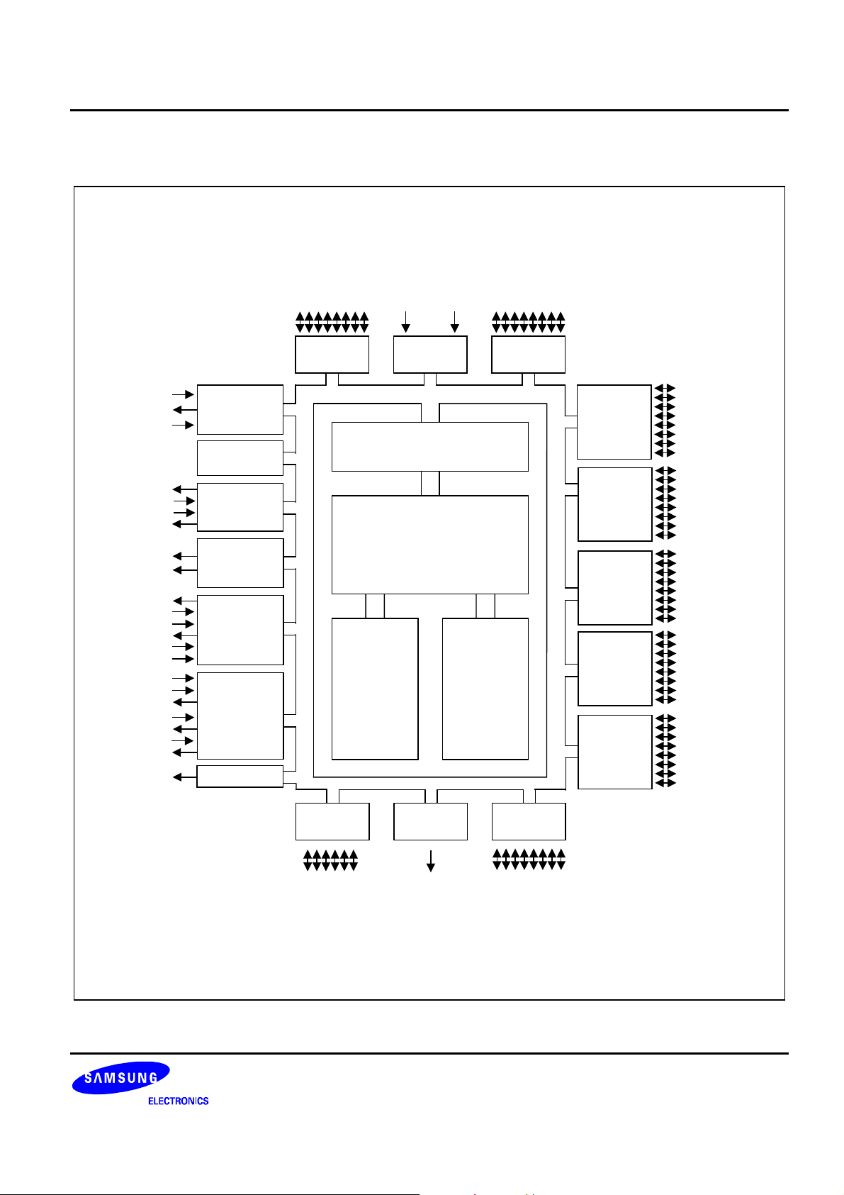
S3C84BB/F84BB PRODUCT OVERVIEW
1 PRODUCT OVERVIEW
S3C8-SERIES MICROCONTROLLERS
Samsung's S3C8-series of 8-bit single-chip CMOS microcontrollers offers a fast and efficient CPU, a wide range
of integrated peripherals, and various mask-programmable ROM sizes. The major CPU features are:
— Efficient register-oriented architecture
— Selectable CPU clock sources
— Idle and Stop power-down mode released by interrupt or reset
— Built-in basic timer with watchdog function
A sophisticated interrupt structure recognizes up to eight interrupt levels. Each level can have one or more
interrupt sources and vectors. Fast interrupt processing (within a minimum of four CPU clocks) can be assigned to
specific interrupt levels.
S3C84BB/F84BB MICROCONTROLLER
The S3C84BB/F84BB single-chip CMOS microcontrollers are fabricated using the highly advanced CMOS
process, based on Samsung’s latest CPU architecture.
The S3C84BB is a microcontroller with a 64K-byte mask-programmable ROM embedded.
The S3F84BB is a microcontroller with a 64K-byte Full-Flash ROM embedded.
Using a proven modular design approach, Samsung engineers have successfully developed the
S3C84BB/F84BB by integrating the following peripheral modules with the powerful SAM8 core:
— Nine programmable I/O ports, including eight 8-bit ports and one 6-bit ports, for a total of 70 pins.
— Ten bit-programmable pins for external interrupts.
— One 8-bit basic timer for oscillation stabilization and watchdog function (system reset).
— Four 8-bit timer/counter and two 16-bit timer/counter with selectable operating modes.
— Tow asynchronous UART
— One synchronous SIO
— One 8-bit D/A converter
— 8-channel A/D converter
The S3C84BB/F84BB is versatile microcontroller for CD-ROM and ADC application, etc. They are currently
available in 80-pin QFP and 80-pin TQFP package.
1-1

PRODUCT OVERVIEW S3C84BB/F84BB
FEATURES
CPU
• SAM88RC CPU core
Memory
• 2064-bytes internal register file
• 64K-bytes internal program memory
- S3C84BB: Mask ROM
- S3F84BB: Flash type memory
Oscillation Sources
• Crystal, Ceramic
• CPU clock divider (1/1, 1/2, 1/8, 1/16)
Instruction Set
• 78 instructions
• IDLE and STOP instructions added for power-
down modes
Instruction Execution Time
• 400 ns at 10-MHz f
(minimum)
OSC
A/D Converter
• 10-bit resolution
• Eight analog input channels
• 20us conversion speed at 10MHz f
ADC
clock.
D/A Converter
• 8-bit D/A Converter
• R/2R Resistor method
• One D/A output (DAOUT)
Asynchronous UART
• Full duplex 2 channels UARTs
• Programmable baud rate
• Supports serial data transmit/receive operations
with 8-bit, 9-bit in UART
Synchronous SIO
• Programmable baud rate
• One synchronous serial I/O module
Interrupts
• 24 interrupt sources with 24 vector.
• 8 level, 24 vector interrupt structure
I/O Ports
• Total 70 bit-programmable pins
Timers and Timer/Counters
• One programmable 8-bit basic timer (BT) for
oscillation stabilization control or watchdog-timer
function.
• One 8-bit timer/counter (Timer A) with three
operating modes; Interval mode, capture mode
and PWM mode.
• One 8-bit timer/counter (Timer B) Carrier
frequency (or PWM) generator.
• Two 8-bit timer with PWM mode (Timer C0,C1)
• Two 16-bit capture timer/counter (Timer 10,11)
with two operating modes; Interval mode,
Capture mode for pulse period or duty.
Pattern Generation Module
• Pattern generation module triggered by timer
match signal and S/W.
Operating Temperature Range
°
• -25
C to + 85°C
Operating Voltage Range
• 2.7 V to 5.5 V at 10MHz f
OSC
Package Type
• 80 pin QFP, 80 pin TQFP
1-2
S3C84BB/F84BB PRODUCT OVERVIEW
BLOCK DIAGRAM
XIN
XOUT
RESETB
P2.7/TAOUT
P2.6/TACAP
P2.5/TACK
P2.4/TBOUT
P3.7/TCOUT0
P3.6/TCOUT1
P3.4/T1OUT0
P3.2/T1CAP0
P3.0/T1CK0
P3.5/T1OUT1
P3.3/T1CAP1
P3.1/T1CK1
P2.2/SCK
P2.1/SI
P2.0/SO
P5.3/RXD0
P5.2/TXD0
P5.1/RXD1
P5.0/TXD1
P0.0~P0.7/
PG0~PG7
OSC/RESETB
8-Bit
Basic Timer
8-Bit
Timer
/CounterA,B
8-Bit
Timer/
CounterC0,C1
16-Bit
Timer
/Counter10,11
SIO/
UART0,1
PG
REF AVSS
AV
Port 0 Port 1A/D
I/O Port and Interrupt Control
SAM88RC CPU
64K-Byte
ROM
P1.0-P1.7P0.0-P0.7
2064-Byte
RAM
Port 2 P2.0-P2.7
Port 3 P3.0-P3.7
Port 4
Port 5 P5.0-P5.7
Port 6 P6.0-P6.7
P4.0-P4.7/
INT0~INT7
Port 8 Port 7D/A
P8.0-P8.5/
INT8,INT9
P2.3/
DAOUT
P7.0-P7.7/
ADC0~ADC7
Figure 1-1. S3C84BB/F84BB Block Diagram
1-3
PRODUCT OVERVIEW S3C84BB/F84BB
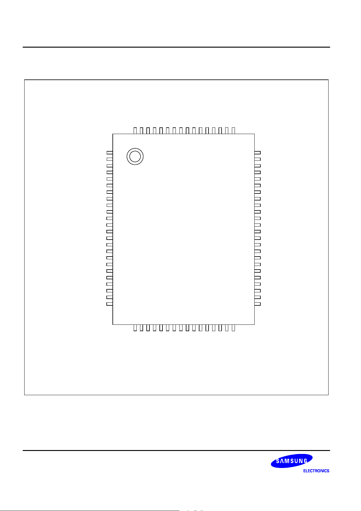
PIN ASSIGNMENT
P0.7/PG7
P0.6/PG6
P0.5/PG5
P0.4/PG4
P0.3/PG3
P0.2/PG2
P0.1/PG1
P0.0/PG0
P1.7
P1.6
P1.5
P1.4
P1.3
P1.2
P1.1
P1.0
65
66
67
68
69
70
71
72
73
74
75
76
77
78
79
80
P2.7/TAOUT
P2.6/TACAP
P2.5/TACK
P2.4/TBPWM
P2.3/DAOUT
P2.2/SCK
P2.1/SI
P2.0/SO
P5.7
P5.6/SDAT
P5.5/SCLK
VDD1
VSS1
XOUT
XIN
TEST
P5.4
P5.3/RxD0
RESETB
P5.2/TxD0
P5.1/RxD1
P5.0/TxD1
P3.7/TCOUT1
P3.6/TCOUT0
1
2
3
4
5
6
7
8
9
10
11
12
13
14
15
16
17
18
19
20
21
22
23
24
S3C84BB/F84BB
(80-QFP-1420C)
252627282930313233343536373839
40
64
63
62
61
60
59
58
57
56
55
54
53
52
51
50
49
48
47
46
45
44
43
42
41
P8.0
P8.1
P8.2
P8.3
P8.4/INT8
P8.5/INT9
P6.0
P6.1
P6.2
P6.3
P6.4
VDD2
VSS2
P6.5
P6.6
P6.7
P7.0/ADC0
P7.1/ADC1
P7.2/ADC2
P7.3/ADC3
AVSS
AVREF
P7.4/ADC4
P7.5/ADC5
P4.7/INT7
P4.6/INT6
P4.5/INT5
P4.4/INT4
P4.3/INT3
P4.2/INT2
P4.1/INT1
P4.0/INT0
P7.7/ADC7
P7.6/ADC6
P3.5/T1OUT1
P3.4/T1OUT0
P3.1/T1CK1
P3.2/T1CAP0
P3.0/T1CK0
P3.3/T1CAP1
Figure 1-2. S3C84BB/F84BB Pin Assignment (80-QFP)
1-4
S3C84BB/F84BB PRODUCT OVERVIEW
PIN ASSIGNMENT
P2.7/TAOUT
P2.6/TACAP
80
79
P0.1/PG1
P0.0/PG0
77
78
P0.2/PG2
76
P0.3/PG3
75
P0.4/PG4
74
P0.5/PG5
73
P0.6/PG6
72
P0.7/PG7
P1.0
70
71
P1.1
69
P1.2
68
P1.3
67
P1.4
66
P1.5
65
P1.6
64
P1.7
63
P8.0
62
P8.1
61
P2.5/TACK
P2.4/TBPWM
P2.3/DAOUT
P2.2/SCK
P2.1/SI
P2.0/SO
P5.7
P5.6/SDAT
P5.5/SCLK
VDD1
VSS1
XOUT
XIN
TEST
P5.4
P5.3/RxD0
RESETB
P5.2/TxD0
P5.1/RxD1
P5.0/TxD1
1
2
3
4
5
6
7
8
9
10
11
12
13
14
15
16
17
18
19
20
S3C84BB/F84BB
(80-TQFP-1212)
21222324252627282930313233343536373839
P4.7/INT7
P4.6/INT6
P4.5/INT5
P4.4/INT4
P4.3/INT3
P4.2/INT2
P4.1/INT1
P4.0/INT0
P7.7/ADC7
P7.6/ADC6
P3.5/T1OUT1
P3.7/TCOUT1
P3.6/TCOUT0
P3.1/T1CK1
P3.3/T1CAP1
P3.4/T1OUT0
P3.0/T1CK0
P3.2/T1CAP0
P7.5/ADC5
40
P7.4/ADC4
60
59
58
57
56
55
54
53
52
51
50
49
48
47
46
45
44
43
42
41
P8.2
P8.3
P8.4/INT8
P8.5/INT9
P6.0
P6.1
P6.2
P6.3
P6.4
VDD2
VSS2
P6.5
P6.6
P6.7
P7.0/ADC0
P7.1/ADC1
P7.2/ADC2
P7.3/ADC3
AVSS
AVREF
Figure 1-3. S3C84BB/F84BB Pin Assignment (80-TQFP)
1-5
PRODUCT OVERVIEW S3C84BB/F84BB
PIN DESCRIPTIONS
Table 1-1. S3C84BB/F84BB Pin Descriptions (80-QFP)
Pin
Name
Pin
Type
Pin
Description
P0.0 - P0.7 I/O Bit programmable port; input or output mode
selected by software; input or push-pull output.
Software assignable pull-up.
Alternately, P0.0-P0.7 can be used as the PG
output port (PG0-PG7).
P1.0 - P1.7 I/O Bit programmable port; input or output mode
selected by software; input or push-pull output.
Software assignable pull-up.
P2.0 - P2.7 I/O Bit programmable port; input or output mode
selected by software; input or push-pull output.
Software assignable pull-up.
Alternately, P2.0~P2.7 can be used as I/O for
TIMERA, TIMERB, D/A, SIO
P3.0 - P3.7 I/O Bit programmable port; input or output mode
selected by software; input or push-pull output.
Software assignable pull-up.
Alternately, P3.0~P3.7 can be used as I/O for
TIMERC0/C1, TIMER10/11
Circuit
Type
Pin
Number
Share
Pins
D 80-73 PG0-PG7
D 72-65
D,D-2 8-1 SO
SI
SCK
DAOUT
TBPWM
TACK
TACAP
TAOUT
D 30–23 T1CK0
T1CK1
T1CAP0
T1CAP1
T1OUT0
T1OUT1
TCOUT0
TCOUT1
1-6
S3C84BB/F84BB PRODUCT OVERVIEW
Table 1-1. S3C84BB/F84BB Pin Descriptions (80-QFP) (Continued)
Pin
Name
P4.0 - P4.7 I/O Bit programmable port; input or output mode
Pin
Type
Pin
Description
Circuit
Type
Pin
Number
D-1 38-31 INT0–
selected by software; input or push-pull output.
Software assignable pull-up.
P4.0-P4.7 can alternately be used as inputs for
external interrupts INT0-INT7, respectively (with
noise filters and interrupt controller)
P5.0 - P5.7 I/O Bit programmable port; input or output mode
G 22-17,11-9 TxD1
selected by software; input or push-pull output.
Software assignable pull-up.
Alternately, P5.0~P5.3 can be used as I/O for serial
por, UART0, UART1, respectively.
P6.0 - P6.7 O N-channel, open-drain output only port. F 58–54,51-49
P7.0 - P7.7 I General-purpose digital input ports. Alternatively
E 48-45,42-39 ADC0used as analog input pins for A/D converter
modules.
P8.0 - P8.5 I/O Bit programmable port; input or output mode
D,D-1 64-59 INT8,INT9
selected by software; input or push-pull output.
Software assignable pull-up.
P8.4, P8.5 can alternately be used as inputs for
external interrupts INT8, INT9, respectively (with
noise filters and interrupt controller)
Share
Pins
INT7
RxD1
TxD0
RxD0
ADC7
1-7
PRODUCT OVERVIEW S3C84BB/F84BB
Table 1-1. S3C84BB/F84BB Pin Descriptions (80-QFP) (Continued)
Pin
Name
AD0 - AD7 I Analog input pins for A/D converter module.
Pin
Type
Pin
Description
Alternatively used as general-purpose digital
Circuit
Type
E 48–45
Pin
Number
P7.0–P7.7
42–39
Share
Pins
input port 7.
AVREF, AVSS - A/D converter reference voltage and ground - 43, 44 -
RxD0, RxD1 I/O Serial data RxD pin for receive input and
D 18, 21 P5.3, P5.1
transmit output (mode 0)
TxD0, TxD1 O Serial data TxD pin for transmit output and
D 20, 22 P5.2, P5.0
shift clock input (mode 0)
TACK I External clock input pins for timer A D 3 P2.5
TACAP I Capture input pins for timer A D 2 P2.6
TAOUT O Pulse width modulation output pins for timer A D 1 P2.7
TBPWM O Carrier frequency output pins for timer B D 4 P2.4
TCOUT0
TCOUT1
T1CK0
O Timer C 8-bit PWM mode output or counter
D 24,23 P3.6,P3.7
match toggle output pins
I External clock input pins for timer 1 D 39,30 P3.0,P3.1
T1CK1
T1CAP0
I Capture input pins for timer 1 D 28,27 P3.2,P3.3
T1CAP1
T1OUT0
T1OUT1
O Timer 1 16-bit PWM mode output or counter
match toggle output pins
D 26,25 P3.4,P3.5
SI,SO,SCK I/O Synchronous SIO pins D 7,8,9 P2.1,P2.0,
P2.2
RESETB I
System reset pin (pull-up resistor: 240 kΩ)
B 19 -
TEST I Pull – down register connected internally - 16 -
VDD1, VDD2,
VSS1, VSS2
- Power input pins - 12,53,
13,52
-
XIN, XOUT - Main oscillator pins - 15,14 -
1-8
 Loading...