


SERVICE MANUAL
MICRO COMPONENT SYSTEM
UX-T550
UX-T550
Contents
Safety precautions
Important for laser products
Preventing static electricity
Disassembly method
Adjustment method
1-2
1-4
1-5
1-6
1-17
This service manual is printed on 100% recycled paper.
COPYRIGHT 2001 VICTOR COMPANY OF JAPAN, LTD.
Flow of functional operation
until TOC read
Maintenance of laser pickup
Replacement of laser pickup
Description of major ICs
Area Suffix
B ------------------------------- U.K.
E ----------- Continental Europe
EN ------------ Northern Europe
EV -------------- Eastern Europe
EE --------- Russian Federation
1-21
1-22
1-22
1-23
No.20908
Jan. 2001

UX-T550
1. This design of this product contains special hardware and many circuits and components specially
for safety purposes. For continued protection, no changes should be made to the original design
unless authorized in writing by the manufacturer. Replacement parts must be identical to those
used in the original circuits. Services should be performed by qualified personnel only.
2. Alterations of the design or circuitry of the product should not be made. Any design alterations of
the product should not be made. Any design alterations or additions will void the manufacturer`s
warranty and will further relieve the manufacture of responsibility for personal injury or property
damage resulting therefrom.
3. Many electrical and mechanical parts in the products have special safety-related characteristics.
These characteristics are often not evident from visual inspection nor can the protection afforded
by them necessarily be obtained by using replacement components rated for higher voltage,
wattage, etc. Replacement parts which have these special safety characteristics are identified in
the Parts List of Service Manual. Electrical components having such features are identified by
shading on the schematics and by ( ) on the Parts List in the Service Manual. The use of a
substitute replacement which does not have the same safety characteristics as the recommended
replacement parts shown in the Parts List of Service Manual may create shock, fire, or other
hazards.
4. The leads in the products are routed and dressed with ties, clamps, tubings, barriers and the
like to be separated from live parts, high temperature parts, moving parts and/or sharp edges
for the prevention of electric shock and fire hazard. When service is required, the original lead
routing and dress should be observed, and it should be confirmed that they have been returned
to normal, after re-assembling.
5. Leakage currnet check (Electrical shock hazard testing)
After re-assembling the product, always perform an isolation check on the exposed metal parts
of the product (antenna terminals, knobs, metal cabinet, screw heads, headphone jack, control
shafts, etc.) to be sure the product is safe to operate without danger of electrical shock.
Do not use a line isolation transformer during this check.
Plug the AC line cord directly into the AC outlet. Using a "Leakage Current Tester", measure
the leakage current from each exposed metal parts of the cabinet , particularly any exposed
metal part having a return path to the chassis, to a known good earth ground. Any leakage
current must not exceed 0.5mA AC (r.m.s.)
Alternate check method
Plug the AC line cord directly into the AC outlet. Use an AC voltmeter having, 1,000 ohms
per volt or more sensitivity in the following manner. Connect a 1,500 10W resistor paralleled by
a 0.15 F AC-type capacitor between an exposed
metal part and a known good earth ground.
Measure the AC voltage across the resistor with the
AC voltmeter.
AC VOLTMETER
(Having 1000
ohms/volts,
or more sensitivity)
Move the resistor connection to eachexposed metal
part, particularly any exposed metal part having a
return path to the chassis, and meausre the AC
voltage across the resistor. Now, reverse the plug in
the AC outlet and repeat each measurement. voltage
measured Any must not exceed 0.75 V AC (r.m.s.).
0.15 F AC TYPE
1500 10W
Place this
probe on
each exposed
metal part.
This corresponds to 0.5 mA AC (r.m.s.).
Good earth ground
1. This equipment has been designed and manufactured to meet international safety standards.
2. It is the legal responsibility of the repairer to ensure that these safety standards are maintained.
3. Repairs must be made in accordance with the relevant safety standards.
4. It is essential that safety critical components are replaced by approved parts.
5. If mains voltage selector is provided, check setting for local voltage.
!
Burrs formed during molding may be left over on some parts of the chassis. Therefore,
pay attention to such burrs in the case of preforming repair of this system.
1-2

(U.K only)
1. This design of this product contains special hardware and many circuits and components specially
for safety purposes. For continued protection, no changes should be made to the original
design unless authorized in writing by the manufacturer. Replacement parts must be identical to
those used in the original circuits.
2. Any unauthorised design alterations or additions will void the manufacturer's guarantee ; furthermore the
manufacturer cannot accept responsibility for personal injury or property damage resulting therefrom.
3. Essential safety critical components are identified by ( ) on the Parts List and by shading on the
schematics, and must never be replaced by parts other than those listed in the manual. Please note
however that many electrical and mechanical parts in the product have special safety related
characteristics. These characteristics are often not evident from visual inspection. Parts other than
specified by the manufacturer may not have the same safety characteristics as the recommended
replacement parts shown in the Parts List of the Service Manual and may create shock, fire, or
other hazards.
4. The leads in the products are routed and dressed with ties, clamps, tubings, barriers and the
like to be separated from live parts, high temperature parts, moving parts and/or sharp edges
for the prevention of electric shock and fire hazard. When service is required, the original lead
routing and dress should be observed, and it should be confirmed that they have been returned
to normal, after re-assembling.
UX-T550
1. Service should be performed by qualified personnel only.
2. This equipment has been designed and manufactured to meet international safety standards.
3. It is the legal responsibility of the repairer to ensure that these safety standards are maintained.
4. Repairs must be made in accordance with the relevant safety standards.
5. It is essential that safety critical components are replaced by approved parts.
6. If mains voltage selector is provided, check setting for local voltage.
!
Burrs formed during molding may be left over on some parts of the chassis. Therefore,
pay attention to such burrs in the case of preforming repair of this system.
1-3

UX-T550
Important for Laser Products
1.CLASS 1 LASER PRODUCT
2.DANGER : Invisible laser radiation when open and inter
lock failed or defeated. Avoid direct exposure to beam.
3.CAUTION : There are no serviceable parts inside the
Laser Unit. Do not disassemble the Laser Unit. Replace
the complete Laser Unit if it malfunctions.
4.CAUTION : The compact disc player uses invisible laser
radiation and is equipped with safety switches which
prevent emission of radiation when the drawer is open and
the safety interlocks have failed or are de
feated. It is dangerous to defeat the safety switches.
VARNING : Osynlig laserstrålning är denna del är öppnad
och spårren är urkopplad. Betrakta ej strålen.
VARO : Avattaessa ja suojalukitus ohitettaessa olet
alttiina näkymättömälle lasersäteilylle.Älä katso
säteeseen.
5.CAUTION : If safety switches malfunction, the laser is able
to function.
6.CAUTION : Use of controls, adjustments or performance of
procedures other than those specified herein may result in
hazardous radiation exposure.
!
Please use enough caution not to
see the beam directly or touch it
in case of an adjustment or operation
check.
ADVARSEL : Usynlig laserstråling ved åbning , når
sikkerhedsafbrydere er ude af funktion. Undgå
udsættelse for stråling.
ADVARSEL : Usynlig laserstråling ved åpning,når
sikkerhetsbryteren er avslott. unngå utsettelse
for stråling.
REPRODUCTION AND POSITION OF LABELS
WARNING LABEL
CLASS 1
LASER PRODUCT
DANGER : Invisibie laser radiation
when open and interlock or
defeated.
AVOID DIRECT EXPOSURE TO
BEAM (e)
VARO : Avattaessa ja suojalukitus
ohitettaessa olet alttiina
näkymättömälle lasersäteilylle.Älä
katso säteeseen. (d)
VARNING : Osynlig laserstrålning är
denna del är öppnad och spårren är
urkopplad. Betrakta ej strålen. (s)
ADVARSEL :Usynlig laserstråling
ved åbning , når
sikkerhedsafbrydere er ude af
funktion. Undgå udsættelse for
stråling. (f)
1-4

UX-T550
Preventing static electricity
Electrostatic discharge (ESD), which occurs when static electricity stored in the body, fabric, etc. is discharged,
can destroy the laser diode in the traverse unit (optical pickup). Take care to prevent this when performing repairs.
1.1. Grounding to prevent damage by static electricity
Static electricity in the work area can destroy the optical pickup (laser diode) in devices such as DVD players.
Be careful to use proper grounding in the area where repairs are being performed.
1.1.1. Ground the workbench
1. Ground the workbench by laying conductive material (such as a conductive sheet) or an iron plate over
it before placing the traverse unit (optical pickup) on it.
1.1.2. Ground yourself
1. Use an anti-static wrist strap to release any static electricity built up in your body.
(caption)
Anti-static wrist strap
Conductive material
(conductive sheet) or iron plate
1.1.3. Handling the optical pickup
1. In order to maintain quality during transport and before installation, both sides of the laser diode on the
replacement optical pickup are shorted. After replacement, return the shorted parts to their original condition.
(Refer to the text.)
2. Do not use a tester to check the condition of the laser diode in the optical pickup. The tester's internal power
source can easily destroy the laser diode.
1.2. Handling the traverse unit (optical pickup)
1. Do not subject the traverse unit (optical pickup) to strong shocks, as it is a sensitive, complex unit.
2. Cut off the shorted part of the flexible cable using nippers, etc. after replacing the optical pickup. For specific
details, refer to the replacement procedure in the text. Remove the anti-static pin when replacing the traverse
unit. Be careful not to take too long a time when attaching it to the connector.
3. Handle the flexible cable carefully as it may break when subjected to strong force.
4. It is not possible to adjust the semi-fixed resistor that adjusts the laser power. Do not turn it
1-5

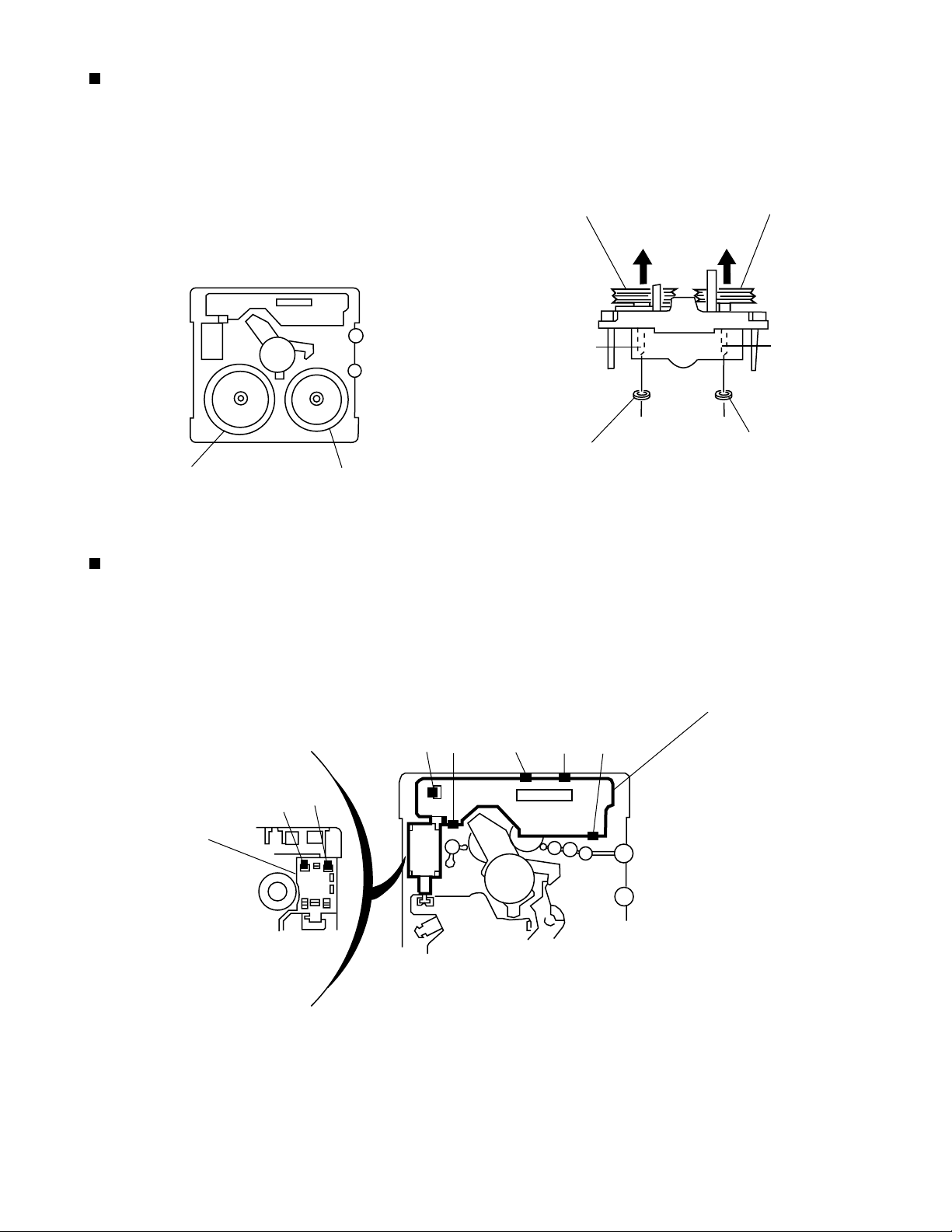
UX-T550
Disassembly method
Removing the rear panel
(See Fig. 1 and 2)
1.
From behind the body, remove the seven screws A
retaining the rear panel.
2.
After turning the body upside down, remove the two
screws B retaining the rear panel.
3.
Take out the rear panel from behind the body.
Removing the side panel (L) and (R)
(See Fig. 2 to 5)
Rear panel
Front panel assembly
C
A
A
A
A
A
Fig. 1
Rear panel
B
1.
After turning the body upside down, remove the two
screws C retaining the front cabinet assembly.
2.
After turning the body back to initial position, open
the CD door while pressing the upper OPEN button.
3.
While moving the side panel (L) in the arrow
direction, remove the panel from the left side of the
body.
4.
While moving the side panel (R) in the arrow
direction, remove the panel from the right side of the
body.
Front panel assembly
Fig. 2
Fig. 3
B
CD door
OPEN button
Front panel assembly
1-6
Side panel (R)
Side panel (L)
Fig. 4Fig. 5

UX-T550
Removing the CD player unit
(See Fig. 6 to 8)
1.
Remove the rear panel.
2.
Remove the left and right side panels.
3.
From the two connector CN603 and CN604 on the CD
servo control board, disconnect the card wires
outgoing from the connector CN304 on the power
amplifier board and the connector CN766 on the LCD
system CPU board.
4.
Disengage the left and right engagements a and b
fixing the CD player unit by using a minus screw
driver, etc.
CD player unit
CD servo
control board
CN604
a
Front panel assembly
CD player unit
CD servo control board
CN603
Fig. 6
Fig. 8
Power amplifier board
CD player unit
b
Front panel assembly
Fig. 7
1-7

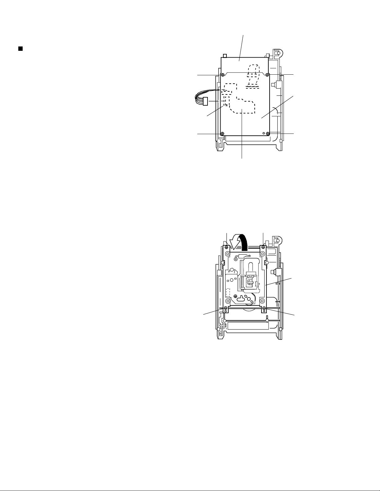
UX-T550
Removing the power amplifier board and
heat sink (See Fig. 9 to 11)
1.
Remove the rear panel.
2.
Remove the left and right side panels.
3.
Remove the CD player unit.
4.
Remove the five screws D and E retaining the heat
sink.
5.
From the connector CN303 on the power amplifier
board, disconnect the card wire outgoing from the
connector CN34 on the head amplifier and
mechanism control board.
6.
From the connector CN901 on the power supply
board, disconnect the connector wire outgoing from
the connector W306 on the power amplifier board.
7.
Remove the one screw F retaining the power
amplifier board.
8.
Remove the power amplifier board from the two
connectors CN711 and CN712 on the LCD system
CPU board.
Heat sink
CN303
D
D
E
Fig. 9
Power amplifier board
CN711
CN712
9.
After removing the power amplifier board from the
key way c on the bottom chassis, take this board out
while raising it in the arrow direction.
LCD system CPU board
Power supply board
Power amplifier board
CN901
Heat sink
Fig. 10
Front panel assembly
1-8
Bttom chassis
c
F
Fig. 11
c

UX-T550
Removing the tuner board
(See Fig. 12 and 13)
1.
Remove the rear panel.
2.
Remove the left and right side panels.
3.
From the right side of the body, remove the one
screw G retaining the tuner board.
4.
From the connector CN1 on the tuner board,
disconnect the card wire outgoing from the connector
CN701 on the LCD system CPU board.
5.
Remove each tuner board backward while releasing
the joint d.
Removing the front panel assembly
(See Fig. 12 and 14)
1.
Remove the rear panel.
LCD system CPU board
CN701
Joint d
CN1
G
Fig. 12
Tuner board
Tuner board
2.
Remove the left and right side panels.
3.
Remove the CD player unit.
4.
Remove the power amplifier board and heat sink.
5.
From the connector CN701 on the LCD system CPU
board, disconnect the card wire outgoing from the
connector CN1 on the tuner board.
6.
From the bottom of the body, disengage the
engagement e fixing the front panel assembly in Fig.
14 while pressing in with a minus screw driver, eta.
Joint d
Front panel assembly
Fig. 13
e
Fig. 14
1-9

UX-T550
Removing the power transformer and
power supply board (See Fig. 15 and 16)
1.
Remove the rear panel.
2.
Remove the left and right side panels.
3.
Remove the CD player unit.
4.
Remove the power amplifier board and heat sink.
5.
Remove the four screws H retaining the power
transformer and power supply board and the one
screw I retaining the jack holder.
Power supply board
Power transformer
HH
Fig. 15
Jack holder
Removing the cassette mechanism unit
(See Fig. 17)
1.
Remove the rear panel.
2.
Remove the left and right side panels.
3.
Remove the CD player unit.
4.
Remove the power amplifier board.
5.
Remove the front panel assembly.
6.
From inside the front panel assembly, remove the
four screws J and K retaining the cassette
mechanism unit.
7.
From the connector CN33 on the head amplifier and
mechanism control board, disconnect the card wire
outgoing from the connector CN731 on the LCD
system CPU board.
Power supply board
LCD system CPU board
CN731
J
I
Fig. 16
Head amplifier & mechanism
control board
CN33
K
1-10
Cassette mechanism unit
Fig. 17

UX-T550
Removing the function switch board and
LCD system CPU board
(See Fig. 18 and 19)
1.
Remove the rear panel.
2.
Remove the left and right side panels.
3.
Remove the CD player unit.
4.
Remove the front panel assembly.
5.
Remove the cassette mechanism unit.
6.
From inside the front panel assembly remove the two
screws L retaining the function switch board.
7.
From the connector CN782 on the LCD system CPU
board, disconnect the connector wire outgoing from
the connector CN802 on the operation switch board.
8.
While sliding the two engagements f fixing the LCD
system CPU board, pull out this board.
Operating switch board
LCD system
CPU board
CN782
f
Function switch board
CN802
L
Fig. 18
Function switch board
L
f
9.
After disconnect the connector CN801 on the
function switch board from the connector CN781 on
the LCD system CPU board, remove the respective
boards while pulling them upward.
LCD system CPU board
Fig. 19
CN801
CN781
1-11

UX-T550
Removing the operating switch board
(See Fig. 20 to 22)
1.
Remove the rear panel.
2.
Remove the left and right side panels.
3.
Remove the CD player unit.
4.
Remove the front panel assembly.
5.
Remove the cassette mechanism unit.
6.
Remove the LCD system CPU board.
7.
Remove the two screws M retaining the operating
switch board.
8.
Remove the MULTI-JOG button.
9.
Remove the VOLUME and POWER / AUX buttons.
10
.
Take out the standby LED lens.
11
.
After removing four pawls g fixing the operating
switch board, remove the switch while pulling it in the
arrow direction.
MULTI-JOG button
M
VOLUME button
Fig. 20
Operating switch board
g
POWER / AUX button
g
M
Standby
LED lens
12
.
Remove the two screws N retaining the operation
switch board.
13
.
Remove the six pawls h fixing the operating switch
board.
h
Operating switch board
N
h
Fig. 21
h
N
h
Fig. 22
1-12

UX-T550
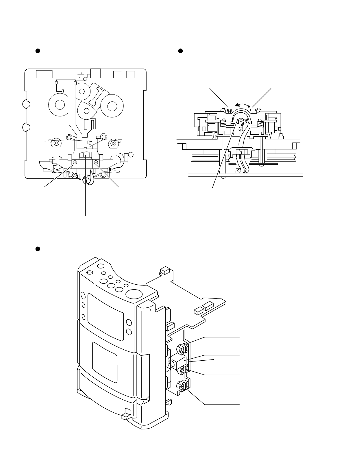
<Cassette mechanism section>
Removing the playback / recording &
eraser head (See Fig. 1 to 3)
1.
While shifting the trigger arms seen on the right side
of the head mount in the arrow direction, turn the
flywheel R in counterclockwise direction until the
head mount has gone out with a click (See Fig. 1).
2.
When the flywheel R is rotated in counterclockwise
direction, the playback / recording & eraser head will
be turned in counterclockwise direction from the
position in Fig. 2 to that in Fig. 3.
3.
At this position, disconnect the flexible P.C. board
(outgoing from the playback / recording & eraser
head) from the connector CN31 on the head
amplifier & mechanism control P.C. board.
4.
Remove the flexible P.C. board from the chassis
base.
5.
Remove the spring 1 from behind the playback /
recording & eraser head.
Flexible
board
Cassette mechanism
Trigger armHead mount
Fig. 1
Playback / Recording &
eraser head
Flywheel R
Spring 1
Trigger arm
6.
Loosen the reversing azimuth screw retaining the
playback / recording & eraser head.
7.
Take out the playback / recording & eraser head from
the front of the head mount.
8.
The playback / recoring & eraser head should also
be removed similarly according to steps 1 to 7 above.
Reassembling the playback / recording &
eraser head (See Fig.3)
1.
Reassemble the playback head from the front of the
head mount to the position as shown in Fig. 3.
2.
Fix the reversing azimuth screw.
3.
Set the spring 1 from behind the playback / recording
& eraser head.
4.
Attach the flexible P.C. board to the chassis base, as
shown in Fig. 3.
5.
The playback / recording & eraser head should also
be reassembled similarly to step 1 to 4 above.
CN31
Head amplifier & mechanism
control P.C. board
Fig. 2
Playback / Recording &
eraser head
Spring 1
Fig. 3
Flywheel R
Reversing azimuth
screw
Head
mount
Flexible
board
Head amplifier &
mechanism control
P.C. board
1-13

UX-T550
Removing the head amplifier & mechanism
control board (See Fig. 4)
1.
Remove the cassette mechanism assembly.
2.
After turning over th cassette mechanism assembly,
remove the three screws A retaining the head
amplifier & mechanism control board.
A
CN32
A
Belt
Main motor
assembly
3.
Disconnect the connector CN32 on the board
including the connector CN 1 on the reel pulse P.C.
board.
4.
When necessary, remove the 4 pin parallel wire
soldered to the main motor.
Removing the main motor assembly
1.
Remove the two screws B retaining the main motor
assembly (See Fig. 4 and 4a).
2.
While raising the main motor, remove the capstan
belt from the motor pulley (See Fig. 4a).
CAUTION:
Be sure to handle the capstan belt so
carefully that this belt will not be stained
by grease and other foreign matter.
Moreover, this belt should be hanged
while referring to the capstan belt
hanging method in Fig. 5 and 6.
Head amplifier &
mechanism control
board
Flexible board
Capstan belt
CN31
A
Fig. 4
Main motor
assembly
B
B
4pin parallel wire
Main
motor
assembly
Motor
pulley
1-14
Capstan
belt
Fig. 5
Fig. 4a
Mechanism motor
assembly
Main motor
assembly
Flywheel
Motor
pulley
Motor pulleyCapstan belt
Fig. 6
Removing the flywheel (See Fig. 7 and 8)
1.
Remove the head amplifier & mechanism control P.C.
board.
2.
Remove the main motor assembly.
3.
After turning over the cassette mechanism, remove
the two slit washers 1 and fixing the capstan shafts R
and L, and pull out the flywheel R and L respectively
from behind the cassette mechanism.
UX-T550
Flywheel R Flywheel L
Capstan shaft R Capstan shaft L
Flywheel R Flywheel L
Fig. 8
Removing the reel pulse P.C. board and
solenoid (See Fig. 9)
1.
Remove the five pawls a to e reattaining the reel
pulse board.
2.
From the surface of the reel pulse board parts,
remove the two pawls f and g retaining the solenoid.
a b c d e
g
f
Solenoid
Slit
washer 1
Slit
washer 1
Fig. 7
Reel pulse board
Fig. 9
1-15
UX-T550
<CD Player Unit Section>
Removing the CD mechanism and CD
servo control P.C. board (See Fig. 1 and 2)
1.
Remove the rear panel.
2.
Remove the left and right side panels.
3.
Remove the CD player unit.
4.
After turning back the CD player unit, remove the
four screws A retaining the CD servo control board
and shield.
5.
From the connector CN601 on the CD servo control
board, disconnect the card wire outgoing from the
CD mechanism.
6.
From the connector P011 on the CD mechanism P.C.
board, disconnect the connector wire outgoing from
the connector CN602 on the CD servo control board.
7.
Remove the four screws B retaining the CD
mechanism.
A
A
P011
Shield
CN601
CN602
CD mechanism board
Fig. 1
A
CD servo
control board
A
8.
While sliding the CD mechanism in the arrow
direction, take turn table out so carefully that it does
not come into contact with the chassis.
B
BB
CD mechanism
B
Fig. 2
1-16

Adjustment method
Measurement instruments required for
adjustment
1. Low frequency oscillator
This oscillator should have a capacity to output
0dBs to 600 at an oscillation frequency of
50Hz-20kHz.
2. Attenuator impedance : 600
3. Electronic voltmeter
4. Distortion meter
5. Frequency counter
6. Wow & flutter meter
7. Test tape
VT712 : Tape speed and running unevenness
(3kHz)
VT724 : Reference level (1kHz)
TMT7036 : Head angle (10kHz), playback
frequency
characteristics (1kHz) and dubbing
frequency
characteristics (63, 1 and 10kHz)
Because of frequency -mixed tape with 63, 1, 10 and
14kHz (250nWb/m - 24dB), use this tape together
with a filter.
8. Blank tape
TYPE : AC-225
TYPE : AC-514
9. Torque gauge : For play and back tension
FWD(TW2111A), REV(TW2121a) and
FF/REW(TW2231A)
Measurement conditions
Power supply voltage
Reference output
Headphone : 0.245V/32
Reference frequency and
input level
Input for confirming recording and
playback characteristics
Measurement output terminal
Load resistance
AC230V (50Hz)
Speaker : 0.775V/4
1kHz, AUX : -8dBs
AUX : -28dBs
Speaker J3002
Tuner section
Voltage applied to tuner +B : DC5.7V
VT : DC 12V
Reference measurement 26.1mV(0.28V)/4
output
Input positions AM : Standard loop antenna
FM : TP1 (hot) and TP2 (GND)
Standard measurement position of volume
Bass Off
Active hoper bass pro Off
Up and down adjustment of volume VOL : 23
Precautions for measurement
1. Apply 30pF and 33k to the IF sweeper output
side and 0.082 F and 100k in series to the
sweeper input side.
2. The IF sweeper output level should be made as
low as possible within the adjustable range.
3. Since the IF sweeper is a fixed device, there is no
need to adjust this sweeper.
4. Since a ceramic oscillator is used, there is no need
to perform any MIX adjustment.
5. Since a fixed coil is used, there is no need to adjust
the FM tracking.
6. The input and output earth systems are separated.
In case of simultaneously measuring the voltage in
both of the input and output systems with an
electronic voltmeter for two channels, therefore, the
earth should be connected particularly carefully.
7. In the case of BTL connection amp., the minus
terminal of speaker is not for earthing. Therefore, be
sure not to connect any other earth terminal to this
terminal. This system is of an BTL system.
8. For connecting a dummy resistor when measuring
the output, use the wire with a greater code size.
9. Whenever any mixed tape is used, use the band
pass filter (DV-12).
4
UX-T550
Radio Input signal
AM frequency 400Hz
AM modulation 30%
FM frequency 400Hz
FM frequency deviation 22.5kHz
1-17
UX-T550
<<Arrangement of adjusting positions>>
Cassette mechanism section
Head azimuth
adjusting screw
(Forward side)
Head azimuth
adjusting screw
(Reverse side)
Cassette mechanism section (Bottom side)
Head azimuth
adjusting screw
(Forward side)
Playback/Recording &
eraser head
Head azimuth
adjusting screw
(Reverse side)
Playback/Recording &
eraser head
Front panel assembly section
VR37
L031
Bias TP
VR31
1-18
VR32

Tape Recorder Section
UX-T550
Items
Confirmation
of head angle
Confirmation
of tape speed
Measurement
conditions
Test tape
: TMT7036 (10kHz)
Measurement output
terminal
: Speaker terminal
Speaker R
(Load resistance: 4 )
: Headphone terminal
Test tape
: VT712 (3kHz) or
TMT7036 (3kHz)
Measurement output
terminal
: Headphone terminal
Measurement method
1 Playback the test tape TMT7036 (10kHz)
2 With the recording & playback mechanism,
adjust the head azimuth screw so that the
forward and reverse output levels become
maximum. After adjustment, lock the head
azimuth at least by half turn.
3 In either case, this adjustment should be
performed in both the forward and reverse
directions with the head azimuth screw.
Adjust VR37 so that the frequency counter
reading becomes 3,010Hz 15Hz when
playing back the test tape VT712 (3kHz) with
playback and recording mechanism after
ending forward winding of the tape.
Reference Values for Confirmation Items
Standard
Values
Maximum
output
Tape speed
of deck
: 3,010Hz
15Hz
Adjusting
positions
Adjust the head
azimuth screw
only when the
head has been
changed.
VR37
Items
Difference
between the
forward and
reverse speed
Wow & flutter Test tape
Measurement
conditions
Test tape
: VT712 (3kHz) or
TMT7036 (3kHz)
Measurement output
terminal
: Speaker terminal
Speaker R
(Load resistance: 4 )
Measurement output
terminal
: Headphone
: VT712 (3kHz) or
TMT7036 (3kHz)
Measurement output
terminal
: Headphone terminal
Measurement method
When the test tape VT712 (3kHz) has been
played back with the recording and playback
mechanism at the beginning of forward
winding, the frequency counter reading of the
difference between both of the mechanism
should be 6.0Hz or less.
When the test tape VT712 (3kHz) has been
played back with the recording and playback
mechanism at the beginning of forward
winding, the frequency counter reading of
wow & flutter should be 0.25% or less
(WRMS).
Standard
Values
6.0Hz or
less
0.25% or
less
(WRMS)
Adjusting
positions
Head azimuth
screw
(See Fig. 34)
1-19

UX-T550
Electrical Performance
Items
Adjustment of
recording bias
current
(Reference
Value)
Adjustment of
recording and
playback
frequency
characteristics
Measurement
conditions
Mode: Forward or
reverse mode
Recording mode
Test tape
: AC-514 to TYPE
and AC-225 to
TYPE
Measurement output
terminal
: Both recording and
headphone terminals
Reference frequency
: 1kHz and 10kHz
(REF.: -20dB)
Test tape
: AC-514 to TYPE
Measurement input
terminal
: OSC IN
Measurement method
1 With the recording and playback
mechanism, load the test tapes (AC-514 to
TYPE and AC-225 to TYPE ), and set
the mechanism to the recording and
pausing condition in advance.
2 After connecting 100 in series to the
recorder head, measure the bias current
with a valve voltmeter at both of the
terminals.
3 After resetting the [PAUSE] mode, start
recording. At this time, adjust VR31 for Lch
and VR32 for Rch so that the recording
bias current values become 4.0 A (TYPE
) and 4.20 A (TYPE ).
1 With the recording and playback
mechanism, load the test tapes (AC-514 to
TYPE ), and set the mechanism to the
recording and pausing condition in
advance.
2 While repetitively inputting the reference
frequency signal of 1kHz and 10kHz from
OSC IN, record and playback the rape.
3 While recording and playback the test tape
in TYPE , adjust VR31 for Lch and VR32
for Rch so that the output deviation
between 1kHz and 10kHz becomes
-1dB 2dB.
Standard
Values
AC-225
: 4.20 A
AC-514
: 4.0 A
Output
deviation
between
1kHz and
10kHz
: -1dB 2dB
Adjusting
positions
L ch
: VR31
R ch
: VR32
L ch
: VR31
R ch
: VR32
Reference Values for Electrical Function Confirmation Items
Items
Recording
bias
frequency
Eraser
current
(Reference
value)
Measurement
conditions
Forward or reverse
Test tape
: TYPE (AC-514)
Measurement
terminal : BIAS TP on
P.C. board
Forward or reverse
Recording mode
Test tape
: AC-514 to TYPE
and AC-225 to
TYPE
Measurement
terminal : Both of the
eraser head terminals
Measurement method
1 While changing over to and from BIAS 1
and 2, confirm that the frequency is
changed.
2 With the recording and playback
mechanism, load the test tape.
(AC-514 to TYPE ), and set the
mechanism to the recording and pausing
condition in advance.
3 Confirm that the BIAS TP frequency on the
P.C. board is 100kHz 6kHz.
1 While recording and playback mechanism,
load the test tapes (AC-514 to TYPE
and AC-225 to TYPE ), and set the
mechanism to the recording and pausing
conditions in advance.
2 After setting to the recording conditions,
connect 1W in series to the eraser head on
the recording and playback mechanism
side, and measure the eraser current from
both of the eraser terminals.
Standard
Values
100 kHz
6 kHz
TYPE
: 120 mA
TYPE
: 75 mA
Adjusting
positions
1-20

Flow of Functional Operation Until TOC Read
Power ON
Power Key
Slider turns REST
SW ON.
Automatic tuning
of TE offset
Check that the voltage at the pin17
of CN604 is 0V (a moment)?
UX-T550
Check Point
Tracking error waveform at TOC reading
pin 25 of
IC601(TE)
Approx
1.8V
VREF
Disc status
to rotate
Approx.3sec
Tracking
servo
off status
Automatic measurement
of TE amplitude and
automatic tuning of
TE balance
Tracking
servo
on status
Disc to be
braked to stop
TOC reading
finishes
500mv/div
2ms/div
Fig.1
Laser ON
Detection of disc
Automatic tuning of
Focus offset
Automatic measurement of
Focus A-curve amplitude
Disc is rotated
Focus servo ON
(Tracking servo ON)
Automatic measurement of
Tracking error amplitude
Automatic tuning of
Tracking error balance
Check that the voltage at the
pin3 of IC601 + side is + 5V?
Confirm that the Focus error
S-cuve signal at the pin27 of
IC601 is approx.2Vp-p
Confirm that the signal from
pin24 IC603 is 0V as a
accelerated pulse during
approx.400ms.
Confirm the waveform of
the Tracking error signal
at the pin25 of IC601 (R612)
(See fig-1)
Automatic tuning of
Focus error balance
Automatic tuning of
Focus error gain
Automatic tuning of
Tracking error gain
TOC reading
Play a disc
Confirm the eys-pattern
at the lead of TP1
1-21

UX-T550
Maintenance of Laser Pickup
(1) Cleaning the pick up lens
Befor you replace the pick up, please try to
clean the lens with a alcohol soaked cotton
swab.
(2) Life of the laser diode (Fig.1)
When the life of the laser diode has expired,
the following symptoms wil appear.
(1) The level of RF output (EFM output:ampli
tude of eye pattern) will below.
Is RF output
1.1 0.15Vp-p?
YES
O.K
NO
Replace it.
Replacement of Laser Pickup
Turn off the power switch and,disconnect the
power cord from the ac outlet.
Replace the pickup with a normal one.(Refer
to " Pickup Removal " on the previous page)
Plug the power cord in,and turn the power on.
At this time,check that the laser emits for
about 3seconds and the objective lens moves
up and down.
Note: Do not observe the laser beam directly.
Play a disc.
(Fig.1)
(3) Semi-fixed resistor on the APC PC board
The semi-fixed resistor on the APC printed
circuit board which is attached to the pickup
is used to adjust the laser power.Since this
adjustment should be performed to match the
characteristics of the whole optical block,
do not touch the semi-fixed resistor.
If the laser power is lower than the specified
value,the laser diode is almost worn out, and
the laser pickup should be replaced.
If the semi-fixed resistor is adjusted while
the pickup is functioning normally,the laser
pickup may be damaged due to excessive current.
Check the eye-pattern at TP1.
Finish.
1-22

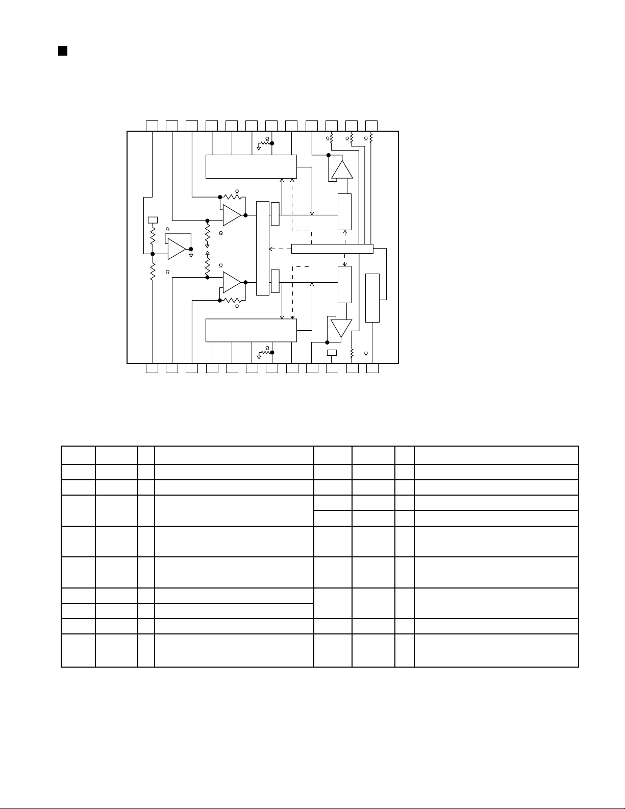
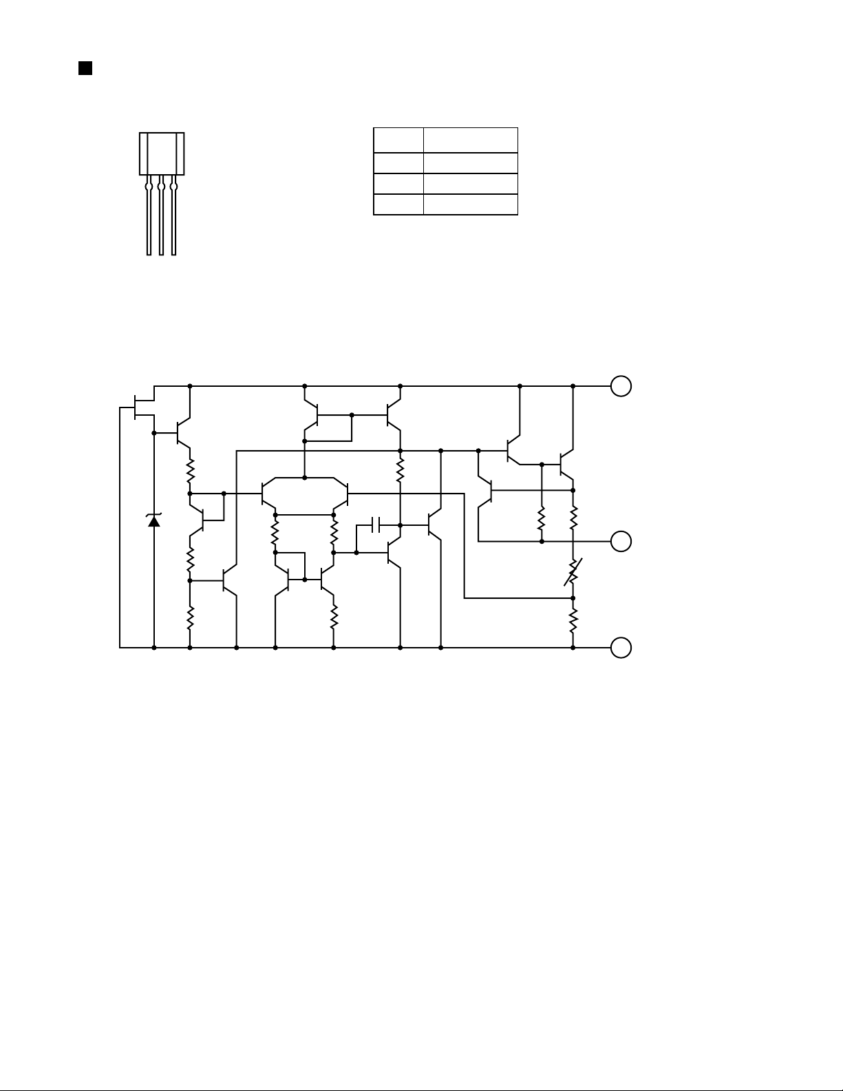
Description of major ICs
AN8806SB (IC601) : RF&Servo AMP
1.Pin layout
PD
LD
LDON
LDP
VCC
RF-
RF OUT
RF IN
C.AGC
ARF
C.ENV
C.EA
CS BDO
BDO
CS BRT
OFTR
/NRFDET
GND
1
2
3
4
5
6
7
8
9
10
11
12
13
14
15
16
17
18
36
35
34
33
32
31
30
29
28
27
26
25
24
23
22
21
20
19
UX-T550
PDAC
PDBD
PDF
PDE
PDER
PDFR
TBAL
FBAL
EF EF OUT
TE TE OUT
CROSS
TE BPF
VDET
LD OFF
VREF
ENV
2.Block diagram
36
-+
35
--
+
31
34
-+
32
33
-+
6
--
VCBA
+
29
728
-+
--
+
+
VCBA
--
+
VCBA
--
--
VCBA
+
+
--
-+
-+
+
--
27
-+
--
EQ
+
+
--
+
--
910 17
8
AGC
OFTR
BDO
RF
DET
11
12 19
ENV CURCUIT
13
14
15
16
-+
20
21
2
24 25
30
14
23
26
22
3
1-23

UX-T550
3. Pin function
AN8806SB
Pin No.
1
2
3
4
5
6
7
8
9
10
11
12
13
14
15
16
17
18
19
20
21
22
23
24
25
26
27
28
29
30
31
32
33
34
35
36
Symbol
PD
LD
LD ON
LDP
VCC
RF-
RF OUT
RF IN
C.AGC
ARF
C.ENV
C.EA
CS BDO
BDO
CS BRT
OFTR
/NRFDET
GND
ENV
VREF
LD OFF
VDET
TE BPF
CROSS
TE OUT
TE-
FE OUT
FE-
FBAL
TBAL
PDFR
PDER
PDF
PDE
PD BD
PD AC
I/O
I
APC amp input terminal
APC amp output terminal
O
APC ON/OFF control terminal
I
--
Connect to ground
Power supply
--
Inverse input pin for RF amp
I
RFamp output
O
RF input
I
Connecting pin of AGC loop filter
I/O
RF output
O
I/O
A capacitor is connected to this terminal to detect the envelope of RF signal
I/O
A capacitor is connected to this terminal to detect the envelope of RF signal
A capacitor is connected to detect the lower envelope of RF signal
I/O
BDO output pin
O
A capacitor is connected to detect the lower envelope of RF signal
I/O
O
Of-track status signal output
RF detection signal output
O
--
Ground
O
Envelope output
Reference voltage output
O
--
Connect to ground
O
Vibration detection signal output
I
Input pin of tracking error through BPF
O
Tracking error cross output
O
Tracking error signal output
Inverse input pin for tracking error amp
I
O
Output pin of focus error
Inverse input pin for focus error amp
I
I
Focus balance control
I
Tracking balance control
F I-V amp gain control
I/O
E I-V amp gain control
I/O
I
I-V amp input
I-V amp input
I
I
I-V amp input
Function
I I-V amp input
1-24

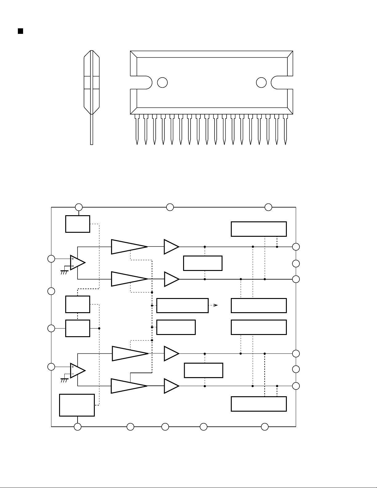
MN35510 (IC603) : Digital servo & digital signal processor
UX-T550
1. Pin layout
2.Block diagram
LRCKIN(MSEL)
BCLK(SSEL)
SRDATAIN
(PSEL)
IOSEL
CLVS
CRC
BLKCK
CLDCK
SBCK
SUBC
DEMPH
RESY
FLAG6(RESY)
SSEL
SQCK
SUBQ
AVDD2
AVDD2
PCK
EFM
PLLF
DSLF
IREF
DRF
ARF
RSEL
PSEL
MLD
MCLK
MDATA
CK384(EFM)
VCOF
BYTCK
SMCK
FCLK
CSEL
MSEL
X2
X1
ÊSTAT
DIGITAL
DEEMPHSIS
SUB
CODE
BUFFER
DSL.
PLL
VCO
VCO
ITUNING
GENERATION
PITCH
CONTROL
20 ~ 1
21
~
40
41 ~ 60
8TIMES
OVER SAMPUNC
DIGITAL FILTER
EFM
DEMODULATION
SYNC
INTERPOLATION
SUBCODE
DEMODULATION
MICRO
COMPUTER
INTERFACE
A/D
COVERTER
80
~
61
1BIT
DAC
LOGIC
S
16k
SRAM
CIRC
ERROR
CORRECTION
DEINTERLEVE
CLV
SERVO
INPUT
PEM
(R)
PEM
(L)
D/A
CONVERTER
OUTPUT
DIGITAL
AUDIO
INTERFASE
DIGITAL
AUDIO
INTERFASE
INTER POLATION
SOFT MUTING DIGITAL
ATTENUATION
PEAK DETECTIVE
AUTO CUE
PORT
SERVO
TIMING GENERATOR
AVSS1
AVDD1
OUTR
OUTL
FLAG
IPFLAG
TX
ECM
PC
LRCK
SRDATA
BCLK
DMUTE
TRKV
KICK
VREF
TRVSTR
ECS
TVD
TRD
FOD
TBAL
FBAL
TOFS
TES
/TLOCK
/FLOCK
PLAY
LDON
WVEL
SENSE
D
/
D
V
V
V
S
D
D
S
D
D
1
/
R
V
T
S
S
E
T
S
S
1
T
F
E
R
T
F
E
E
N
V
T
R
C
R
S
B
V
D
D
O
E
T
/
R
F
D
E
O
F
T
1-25

UX-T550
3. Pin function
Pin
No.
1
2
3
4
5
6
7
8
9
10
11
12
13
14
15
16
17
18
19
20
21
22
23
24
25
26
27
28
29
30
31
32
33
34
35
36
37
38
39
40
symbol
BCLK
LRCK
SRDATA
DVDD1
DVSS1
TX
MCLK
MDATA
MLD
SENSE
FLOCK
TLOCK
BLKCK
SQCK
SUBQ
DMUTE
STATUS
RST
SMCK
PMCK
TRV
TVD
PC
ECM
ECS
KICK
TRD
FOD
VREF
FBAL
TBAL
FE
TE
RF ENV
VDET
OFT
TRCRS
RFDET
BDO
LDON
I/O
O
O
O
I
I
O
I
I
I
O
O
O
O
I
O
O
I
I
O
O
O
O
O
O
O
I
O
O
I
I
I
I
I
I
I
I
O
Function
Not used
Not used
Not used
Power supply (Digital)
Connected to GND
Digital audio interface output
com command clock signal input
(Data is latched at signal's rising point)
com command data input
com command load signal input
Not used
Not used
Not used
sub-code block clock signal output
Outside clock for sub-code Q resister input
Sub-code Q -code output
I
Connected to GND
Status signal
(CRC,CUE,CLVS,TTSTOP,ECLV,SQOK)
Reset signal input (L:Reset)
Not used
I
Not used
Traverse enforced output
Traverse drive output
I
Not used
Spindle motor drive signal (Enforced
mode output) 3-State
Spindle motor drive signal (Servo error
signal output)
Kick pulse output
Tracking drive output
Focus drive output
Reference voltage input pin for D/A
output block (TVD,FOD,FBA,TBAL)
Focus Balance adjust signal output
Tracking Balance adjust signal output
Focus error signal input(Analog input)
Tracking error signal input(Analog input)
RF envelope signal input(Analog input)
Vibration detect signal input(H:detect)
Off track signal input(H:off track)
Track cross signal input
RF detect signal input(L:detect)
BDO input pin(L:detect)
Laser ON signal output(H:on)
Pin
No.
41
42
43
44
45
46
47
48
49
50
51
52
53
54
55
56
57
58
59
60
61
62
63
64
65
66
67
68
69
70
71
72
73
74
75
76
77
78
79
80
symbol
TES
PLAY
WVEL
ARF
IREF
DRF
DSLF
PLLF
VCOF
AVDD2
AVSS2
EFM
PCK
PDO
SUBC
SBCK
VSS
XI
X2
VDD
BYTCK
CLDCK
FCLK
IPPLAG
FLAG
CLVS
CRC
DEMPH
RESY
IOSEL
TEST
AVDD1
OUT L
AVSS1
OUT R
RSEL
CSEL
PSEL
MSEL
SSEL
I/O
Tracking error shunt signal output(H:shunt)
O
I
Not used
I
Not used
I
RF signal input
Reference current input pin
I
Bias pin for DSL
I
I/O
Loop filter pin for DSL
Loop filter pin for PLL
I/O
I
Not used
I
Power supply(Analog)
Connected to GND(Analog)
Not used
II I
Not used
I
Not used
I
Not used
I
Not used
Connected to GND(for X'tal oscillation
I
circuit)
Input of 16.9344MHz X'tal oscillation circuit
I
Output of X'tal oscillation circuit
O
I
Power supply(for X'tal oscillation circuit)
I
Not used
I
Not used
I
Not used
I
Not used
I
Not used
I
Not used
I
Not used
Not used
I
Not used
III
pull up
pull up
Power supply(Digital)
Lch audio output
O
I
Connected to GND
Rch audio output
O
II
pull up
Connected to GND
I
Connected to GND
I
Connected to GND
I
Pull up
Function
MN35510
1-26
BH3852S (IC38) : E.Volume
1. Block diagrams
FILTER
IN2
NF2
BVN2
24 23 22 21 20 19 18 17 16 15 14 13
BIN2
BVO2
TIN2
2K
(BASS) (TREBLE)
TONE CONTROL
20K
TVO2
OOUT2VCTC
10M 10M 10M
UX-T550
BC
- +
Vcc
20K
+
20K
1 2 3 4 5 6 7 8 9 10 11 12
IN1
GND
+
47K
47K
+
-
20K
TONE CONTROL
(BASS) (TREBLE)
NF1
BVN1
MATRIX SURROUND SOUND
VOLUME VOLUME
2K
BVO1
TIN1
BIN1
TVO1
CONTROL
- +
Vcc
Vcc
OUT1
2. Pin function
Function
13
14
15
16
17.18
1
2
3
Symbol
GND
IN1
NF1
I/O
Connect to GND.
Terminal for 1ch volume input.
I
Terminal for gain adjustment of
I
Pin No. Pin No.
input step AMP.
4~6
BASS1
Terminal for connection of 1ch
low-frequency filter.
7.8
TRE1
Terminal for connection of 1ch
-
19~21
high-frequency filter.
9
10
11
12
OUT1
VCC
LIVE
VREF
Terminal for 1ch volume output.
O
Terminal for power supply.
Terminal for surround control.
Terminal for reference voltage
O
22
23
24
output.
VOLUMEVOLUME
10M
SC
Symbol
BASS
TRE
VOL
OUT2
TRE2
BASS2
NF2
IN2
VSET
Ref. Voltage
VREF
I/O
I
I
I
O
-
-
I
I
-
Function
Terminal for bass control.
Terminal for treble control.
Terminal for volume control.
Terminal for 2ch volume output.
Terminal for connection of 2ch
high-frequency filter.
Terminal for connection of 2ch
low-frequency filter.
Terminal for gain adjustment of
input step AMP.
Terminal for 2ch volume input.
Terminal for filter.
1-27

UX-T550
BU4094BCF-X (IC33) : SHIFT / STORE register
1. Pin layout
16 15 14 13 12 11 10 9
VDD Q5 Q6 Q7 Q8 Q'S QS
STROBE DATA CLOCK Q1 Q2 Q3 Q4 Vss
OUTPUT
ENABLE
1 2 3 4 5 6 7 8
2. Block diagram
DATA
CLOCK
STROBE
OUTPUT
ENABLE
2
8-STAGE
3
1
SHIFT REGISTER
8-BIT
LATCHES
15
3-STATE
OUTPUTS
Q1 Q8
10
9
Q'S
QS
SERIAL
OUTPUT
1-28
PARALLEL OUTPUT
KIA78S06P (IC703) : Regulator
UX-T550
1.Pin layout
123
3.Block diagram
Q14
Z1
R9
Q16
R10
Q1
Q2
Q7
Q4
R1
2. Pin function
Q3
Q6
R2
Q8
Pin No.
C1
1
2
3
Q5
R4
Q9
Function
Output
Common
Input
Q11
Q10
Q12
R8
Q13
R7
R5
3
INPUT
2
OUTPUT
R11
R3
R6
1
COMMON
1-29
UX-T550
LA4705NA (IC31) : 2ch BTL power IC
1. Pin layout
2. Block diagram
LA4705N
123456789101112131415161718
GND
2
4
5
7
RIPPLE
FILTER
IN
BIAS
CIRCUIT
STANDBY
SW
IN
PREDRIVER
PREDRIVER
PREDRIVER
NC Vcc1
OUTPUT PIN TO Vcc
POWER
LOAD SHORT
PROTECTOR
POWER
OVER VOLTAGE/
SURGE PROTECTOR
THERMEL
SHUTDOWN
POWER
LOAD SHORT
PROTECTOR
SHORT PROTECTOR
OUTPUT PIN TO GND
Vcc
SHORT PROTECTOR
OUTPUT PIN TO GND
SHORT PROTECTOR
1813
17
POWER
16
GND1
15
14
POWER
13
GND2
1-30
POP NOISE
PREVENTION
CIRCUIT
PREDRIVER
POWER
OUTPUT PIN TO Vcc
SHORT PROTECTOR
68910 11
Vcc2NCNC
12

LC72136N (IC2) : PLL frequency synthesizer
1. Pin layout
FM/AM
CLOCK
FM/ST/VCO
AM/FM
2. Block diagram
XT
CE
DI
DO
SDIN
1
2
3
4
5
6
7
8
9
10
11
22
21
20
19
18
17
16
15
14
13
12
XT
GND
LPFOUT
LPFIN
PD
VCC
FMIN
AMIN
IFCONT
IFIN
UX-T550
1
22
16
15
3
4
5
6
17
21
3. Pin function
Pin
Symbol
No.
1
2
3
4
5
6
7
8
9
10
11
XT
FM/AM
CE
DI
CLOCK
DO
FM/ST/VCO
AM/FM
LW
MW
SDIN
Reference
Driver
Swallow Counter
1/2
C
2
B
I/F
Powe r
on
Reset
Function
I/O
X'tal oscillator connect (75kHz)
I
LOW:FM mode
O
When data output/input for 4pin(input) and
I
Swallow Counter
1/16,1/17 4bit
1/16,1/17 4bit
12bit
Programmable
DriverS
Data Shift Register & Latch
7821113
6pin(output): H
Input for receive the serial data from
I
controller
Sync signal input use
I
Data output for Controller
O
Output port
"Low": MW mode
O
Open state after the power on reset
O
Input/output port
I/O
Input/output port
I/O
Data input/output
I/O
Phase
Detector
Charge Pump
Unlock
Detector
Universal
Counter
Pin
Symbol
No.
12
IFCONT
13
14
15
16
17
18
19
LPFOUT
20
21
22
IFIN
AMIN
FMIN
VCC
PD
LPFIN
GND
XT
18
19
20
12
I/O
Function
IF counter signal input
I
IF signal output
O
Not use
-
AM Local OSC signal output
I
FM Local OSC signal input
I
Power suplly(VDD=4.5-5.5V)
When power ON:Reset circuit move
PLL charge pump output(H: Local OSC
O
frequency Height than Reference frequency.
L: Low Agreement: Height impedance)
Input for active lowpassfilter of PLL
I
Output for active lowpassfilter of PLL
O
Connected to GND
X'tal oscillator(75KHz)
I
1-31

UX-T550
TA2057N (IC1) : FM / AM IF AMP & Detector
1.Block d iagrams
FM
IF IN
24 23 22 21 20 19 18 17 16 15 14 13
AM
MIX
OUT Vstb QUAD FM OUT AM OUT MPX IN LPF 1 LPF 2 VCO L OUT
AM
IF IN
AM
MIX
123456789 1110 12
AM
RF IN
2.Pin function
Pin
No.
I/O
1
I
2
3
4
-
5
6
7
8
9
10
11
12
AM OSC OUT
O
-
I
-
O
O
O
O
REG
FM
IF
S.SENSFMS.SENS
Symbol
AM RF
AM S.SENS
FM S.SENS
AM OSC
VCC
AGC
GND
IF OUT
TU IND
ST IND
Rch OUT
FM
DET
AM
IF
AM
OSC
AM
OSCAMOSC
AMRF signal input
AM local oscillation circuit
AM local oscillation signal output
Power supply
AGC voltage input terminal
Connect to GND
IF REQ signal output to IC2
Indicator drive output when tuning
Stereo indicator output
"H"mono . "L"stereo
Output Rch
BUFF
Vcc AGC GND IF OUT
OUT
Function Function
AM
DET
Pin
No.
13
14
15
16
17
18
19
20
21
22
23
24
AGC
I/O
O
O
O
O
I
O
O
I
I
-
O
I
AM
LEVEL
SW
IF
BUFF
IF REQ
SW
Symbol
Lch OUT
VCO
LPF2
LPF1
MPX IN
AM OUT
FM OUT
FM QUAD
AM IF IN
Vst
AM MIX OUT
FM IF IN
VCO
DIVIDE
DECODE
AM/FM
MONO
SW
TUN
LED
/REQ
TUN
LED
Output Lch
Voltage controlled terminal
When voltage of terminal is MONO
at "H" and ST at "L"
When voltage of terminal is AM at
"H" and FM at "L"
Multi plex signal input
AM detection signal output
FM detection signal output
Bypass to FMIF
Input of AMIF signal
Fixed voltage output terminal
Output terminal for AM mixer
Input of FMIF signal
ST
LED
ST
LED
MUTE
R OUTAM
1-32

UPD78064GF-149 (IC701) : System CPU
1.Pin layout
100 ~ 81
1
80
UX-T550
~
30
31 ~ 50
2.Pin function
Pin
Symbol
No.
USDATA
1
USCK
2
UQRIN
3
UNC
4
USQCK
5
ICVSS
6
UX2
7
UX1
8
VDD
9
UXT1
10
UXT2
11
URESET
12
UREM
13
URDSCK
14
UJOG1
15
UBEAT2
16
UBEAT1
17
U+BCTL
18
UXRESET
19
UMCLK
20
UMDATA
21
UMLD
22
UPBMUTE
23
ULATCH
24
UREEL
25
UFAUX
26
UAVSS
27
USAFEYCD
28
~
51
I/O
I/O
Serial data
Serial clock
O
CD Q code data
I
Non connect
-
CD Q code data synchronizing clock
O
Connected to VSS
-
Main system clock
-
Main system clock
I
Power supply
-
Sub system clock
I
Sub system clock
-
Reset
I
Remote control
I
Non connect
-
Jog encoder 1
I
Main clock selection 2
O
Main clock selection 1
O
Switched 5V control
O
CD LSI reset
O
CD LSI command clock
O
CD LSI command data
O
CD LSI command load
O
Tape playback mute
O
Tape IC strobe
O
Tape end detection
I
Function AUX
O
AD converter GND
-
CD abnormal voltage detection
I
Function
Pin
No.
29
30
31
32
33
34
35
36
37
38
39
40
41
42
43
44
45
46
47
48
49
50
51~54
55
56~58
59
60~99
100
Symbol
URESET/CLOSE
USAFETY1
USAFETY0
UKEY1
UKEY0
UTAPE0
UTAPE1
AVDD
UAVREF
UBUP
UFTUNER
VSS
UMPX
UPERIOD
UJOGB
UBASS
UTRE
UVOL
USBASS
USMUTE
UPOUT
UFCD
COM0~3
BIAS
VLC0~2
VSS
S0~39
USTATUS
I/O
[RESET/CLOSE] switch
I
Abnormal voltage detection 1
I
Abnormal voltage detection 2
I
Body key input 1
I
Body key input 0
I
Tape switch 0
I
Tape switch 1
I
AD converter power supply
-
AD converter reference voltage
-
Backup power supply decision
I
Function tuner
O
GND
-
FM stereo detection
I
Tuner PLL strobe
O
JOG encoder 2
I
BASS control
O
TRE control
O
VOL.control
O
AHB on/off
O
System muting
O
Power ON/OFF
O
Function CD
O
LCD common
O
LCD bias voltage
-
LCD bias voltage
-
GND
-
LCD segment
O
LCD LSI status
I
Function
1-33

UX-T550
AN7317 (IC32) : Pre Amp.
1. Pin layout & Block diagram
16 15 14 13 12 11 10 9
Pre-in Pre-NF Pre-out Rec-in Rec-out Rec-Mute R.R. Vcc
1 2 3 4 5 6 7 8
2. Pin function
Pin No.
1
2
3
4
5
6
7
8
9
10
11
12
13
14
15
16
Pre
Pre
Rec
Rec
ALC
MUTE R.R.
Pre-in Pre-NF Pre-out Rec-in Rec-out GND
ALC
Low-cut
ALC
Time
Function
Channel 1 playback amplifier input
Channel 1 playback amplifier negative feedback
Channel 1 playback amplifier output
Channel 1 recording amplifier input
Channel 1 recording amplifier output
ALC low-cut
ALC time
Ground
Vcc
Ripple filter
Record amplifier mute
Channel 2 record amplifier output
Channel 2 record amplifier input
Channel 2 playback amplifier output
Channel 2 playback amplifier negative feedback
Channel 2 playback amplifier input
BA3126N (IC31) : Head select switch
1. Pin layout & Block diagram
REC
SW
G
P/B
SW
CONT.
1 2 3 4 5 6 7 8 9
1-34
GND
Vcc
P/B
SW
G
REC
SW

BA6897FP (IC602) : 4channel driver
1.Pin layout
UX-T550
CH1-OUTA
CH1-OUTB
CH1-INA
CH1-INB
TEST1
TEST2
MUTE
CH2-INB
CH2-INA
CH2-OUTB
CH2-OUTA
GND
D.BUF
1
2
D.BUF
3
4
5
6
7
8
9
10
D.BUF
11
12
D.BUF
13
- +
Level
shift
-+
+-
Level
shift
- +
T.S.D
DRIVER
MUTE
+ Level
shift
Level
shift
+ -
D.BUF
D.BUF
+-
-+
-+
D.BUF
D.BUF
28
27
26
25
24
23
22
21
20
19
18
CH3-OUTB
17
CH3-OUTA
16
OP IN(+)
GND
CH4-OUTA
CH4-OUTB
CH4-INA
CH4-INB
BIAS IN
Vcc
Vcc
CH3-INB
CH3-INA
OP-OUT
14
-+
15
OP IN(-)
BA15218N (IC32 / IC35) : Dual Ope. Amp.
+
+
1
-
1 2 3 4 5 6 7 8
OUT1 +IN1 +IN1
+IN2 -IN2 OUT2
GND
2
-
Vcc
1-35

UX-T550
VICTOR COMPANY OF JAPAN, LIMITED
AUDIO & COMMUNICATION BUSINESS DIVISION
PERSONAL & MOBILE NETWORK BUSINESS UNIT. 10-1,1chome,Ohwatari-machi,Maebashi-city,371-8543,Japan
(No.20908)
Printed in Japan
200101(V)
 Loading...