

Page 1
SERVICE MANUAL
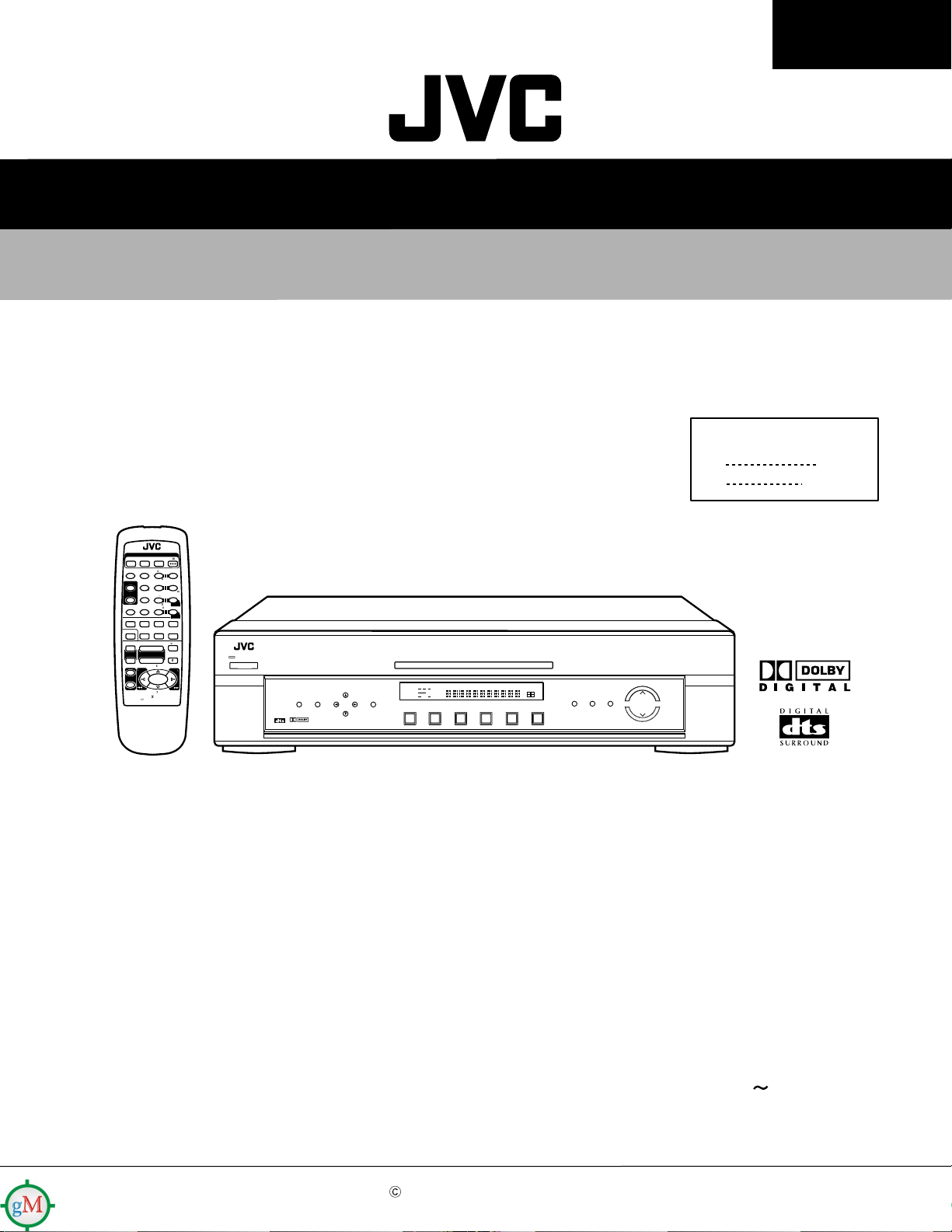
AUDIO/VIDEO CONTROL RECEIVER
RX-E100SL
Area Suffix
RX-E100SL
POWER
TV
DVD
VCR
– SUBWOOFER +TESTSLEEP
1
5
SURROUND
EFFECT
– CENTER +
54
5
BASS
– REAR•L +
DSP MODE
BOOST
7
5
SOUND
– REAR•R +
010
DVD
TV
VCR
TV/VIDEO
FM
CD
+
+
TV VOL
VOLUME
–
–
£
1
+
+
TV/VCR
CH
–
7
RM-SRXE100J
REMOTE CONTROL
HOME THEATER RECEIVER
J
C
AUDIO
32
6
5
98
MENU
+10
ENTER
INPUT A/D
AM
MUTING
8
1
POWER
STANDBY
TV DILECT
CONTROL
ADJUST
SETTING
DIGITAL
DIGITAL
SURROUND
ANALOG
LPCM
DOLBY D
DTS
MEMORY
DVD
DVD TV VCR CD FM
HOME THEATER RECEIVER
RX-E100
PRO LOGIC
LCR
SLEEP STTUNED MUTING
DSP
SUBWFRLFE
DGTL AUTO
LS S RS
INPUT ATT
AUTO
Z
MH
KHZ
VOL
AM
INPUT
ANALOG/DIGITAL
INPUT ATT
SURROUND
ON/OFF
DSP
MODE
MASTER VOLUME
U.S.A
Canada
Contents
Safety precautions --------------------------------------------------------1- 2
Importance administering point on the safety ---------------------1- 3
Disassembly method -----------------------------------------------------1- 4
Adjustment method -------------------------------------------------------1- 9
Description of major ICs -------------------------------------------------1-10 16
COPYRIGHT 2001 VICTOR COMPANY OF JAPAN, LTD.
No.20955
May 2001
Page 2
http://getMANUAL.com
RX-E100SL
1. This design of this product contains special hardware and many circuits and components specially for safety
purposes. For continued protection, no changes should be made to the original design unless authorized in
writing by the manufacturer. Replacement parts must be identical to those used in the original circuits. Services
should be performed by qualified personnel only.
2. Alterations of the design or circuitr y of the product should not be made. Any design alterations of the product
should not be made. Any design alterations or additions will void the manufacturer`s warranty and will fur ther
relieve the manufacture of responsibility for personal injury or property damage resulting therefrom.
3. Many electrical and mechanical parts in the products have special safety-related characteristics. These
characteristics are often not evident from visual inspection nor can the protection afforded by them necessarily
be obtained by using replacement components rated for higher voltage, wattage, etc. Replacement par ts which
have these special safety characteristics are identified in the Parts List of Service Manual. Electrical
components having such features are identified by shading on the schematics and by ( ) on the Parts List in
the Service Manual. The use of a substitute replacement which does not have the same safety characteristics
as the recommended replacement parts shown in the Parts List of Service Manual may create shock, fire, or
other hazards.
4. The leads in the products are routed and dressed with ties, clamps, tubings, barriers and the like to be
separated from live parts, high temperature parts, moving parts and/or sharp edges for the prevention of
electric shock and fire hazard. When service is required, the original lead routing and dress should be
observed, and it should be confirmed that they have been returned to normal, after re-assembling.
5. Leakage currnet check (Electrical shock hazard testing)
After re-assembling the product, always perform an isolation check on the exposed metal parts of the product
(antenna terminals, knobs, metal cabinet, screw heads, headphone jack, control shafts, etc.) to be sure the
product is safe to operate without danger of electrical shock.
Do not use a line isolation transformer during this check.
Plug the AC line cord directly into the AC outlet. Using a "Leakage Current Tester", measure the leakage
current from each exposed metal parts of the cabinet, particularly any exposed metal part having a return
path to the chassis, to a known good earth ground. Any leakage current must not exceed 0.5mA AC (r.m.s.).
Alternate check method
Plug the AC line cord directly into the AC outlet. Use an AC voltmeter having, 1,000 ohms per volt or more
sensitivity in the following manner. Connect a 1,500 10W resistor paralleled by a 0.15 F AC-type capacitor
between an exposed metal part and a known good earth ground.
Measure the AC voltage across the resistor with the AC
voltmeter.
Move the resistor connection to eachexposed metal part,
particularly any exposed metal part having a return path to
the chassis, and meausre the AC voltage across the resistor.
Now, reverse the plug in the AC outlet and repeat each
measurement. voltage measured Any must not exceed 0.75 V
AC (r.m.s.). This corresponds to 0.5 mA AC (r.m.s.).
0.15 F AC TYPE
1500 10W
Good earth ground
AC VOLTMETER
(Having 1000
ohms/volts,
or more sensitivity)
Place this
probe on
each exposed
metal part.
!
1. This equipment has been designed and manufactured to meet international safety standards.
2. It is the legal responsibility of the repairer to ensure that these safety standards are maintained.
3. Repairs m ust be made in accordance with the relevant safety standards.
4. It is essential that safety critical components are replaced by approved parts.
5. If mains voltage selector is provided, check setting for local voltage.
Burrs formed during molding may
be left over on some parts of the
chassis. Therefore, pay attention to
such burrs in the case of
preforming repair of this system.
In regard with component parts appearing on the silk-screen pr inted side (parts side) of the PWB diagrams, the
parts that are printed over with black such as the resistor ( ), diode ( ) and ICP ( ) or identified by the " "
mark nearby are critical for safety.
When replacing them, be sure to use the parts of the same type and rating as specified by the manufacturer.
(Except the JC version)
1-2
Page 3
Importance administering point on the safety
EP202
LVA10230-A3
TA201
TA202
R205
RX-E100SL
FW201
FW202
FC203
2A-125V
FC204
FC205
2A-125V
FC206
FC201
B410
B411
B413
B412
B414
PW103 PW102 PW101
FC202
5A-125V
B415
CN217
R201
CN207
LVA10230-A2
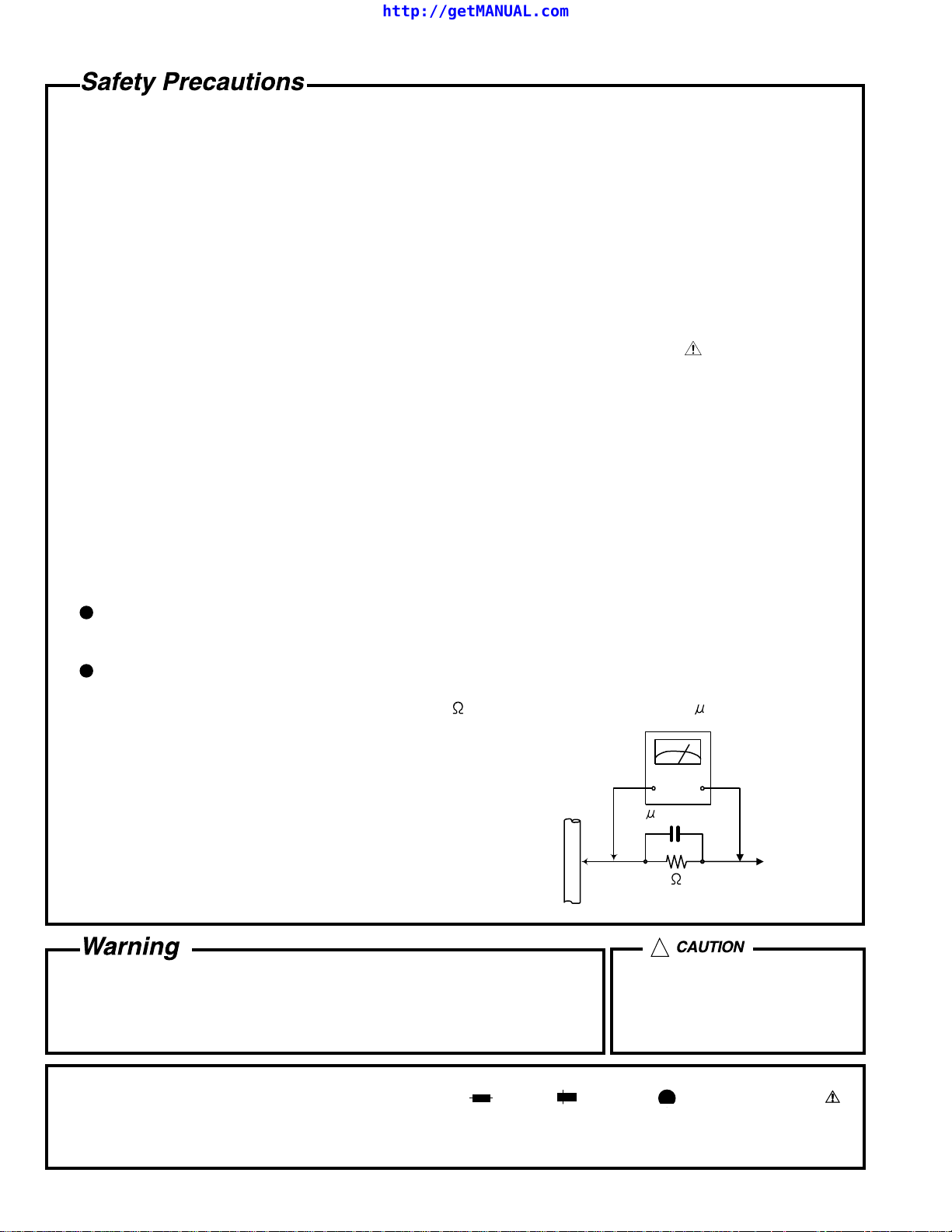
Caution: For continued protection against risk of
fire, replace only with same type 5A/125V for
F201, 2A/125V for F202 and F203. This symbol
specifies type of fast operating fuse.
Precaution: Pour eviter risques de feux, remplacez
le fusible de surete de F201 comme le meme type
que 5A/125V, et 2A/125V pour F202 et F203.
Ce sont des fusibles suretes qui functionnes rapide.
^
1-3
Page 4
RX-E100SL
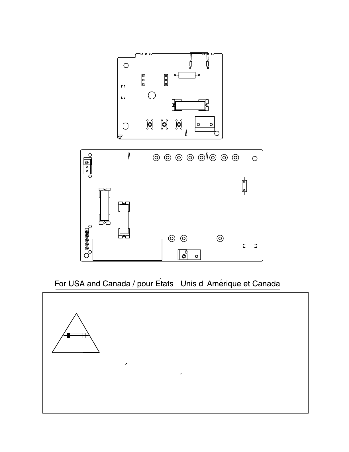
Disassembly method
Removing the top cover (See Fig.1)
1.
Remove the four screws A attaching the top cover
on both sides of the body.
2.
Remove the three screws B on the back of the body.
3.
Remove the top cover from behind in the direction of
the arrow while pulling both sides outward.
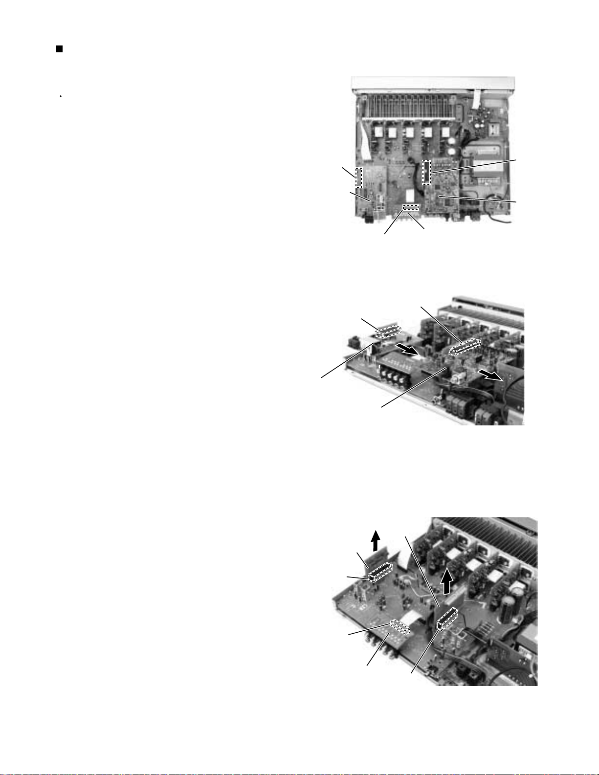
Removing the front panel assembly
(See Fig.2 and 3)
Prior to performing the following procedure, remove
the top cover.
1.
Disconnect the card wire from connector CN411 on
the audio board and CN204 on the power supply
board in the front panel assembly.
2.
Cut off the tie band fixing the harness.
A
Tie band
Main
board
CN411
Audio
board
Top cover
2
A
B
2
C
Fig.1
Front panel assembly
C
CN204
Power supply
board
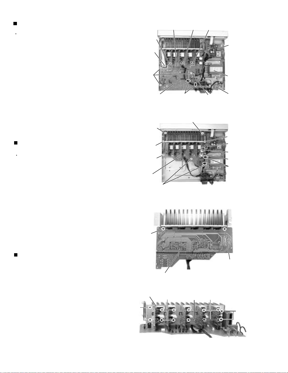
3.
Remove the three screws C attaching the front
panel assembly.
4.
Remove the four screws D attaching the front panel
assembly on the bottom of the body. Detach the front
panel assembly toward the front.
Removing the rear panel (See Fig.4)
Prior to performing the following procedure, remove
the top cover.
1.
Remove the power cord stopper from the rear panel
by moving it in the direction of the arrow.
2.
Remove the eleven screws E attaching the each
boards to the rear panel on the back of the body.
E
Rear panel
D
Fig.2
Fig.3
Front panel assembly
D
E
Cord stopper
3.
Remove the four screws F attaching the rear panel
on the back of the body.
1-4
F
E
F
Fig.4
E
F
F
Page 5
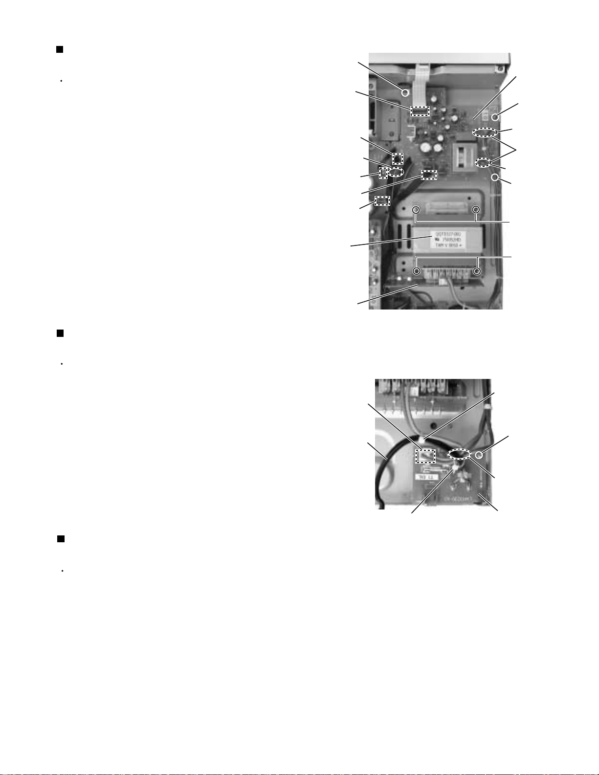
Removing each board connected to the
rear side of the audio board
(See Fig.5 to 7)
Prior to performing the following procedure, remove
the top cover and the rear panel.
1.
Cut off the tie band fixing the harness.
2.
Disconnect the tuner board and DSP board from
connector CN111 and CN681 on the each Relay
board.
3.
Disconnect the Relay board from connector CN503
and CN501 on the audio board.
4.
Disconnect the card wire connected to connector
CN522 on the Input board.
CN111
Tuner
board
CN522
RX-E100SL
CN681
DSP
board
Input
board
Fig.5
Tuner
board
CN503
CN111
CN681
DSP board
Fig.6
Relay
board
Relay
board
CN522
Input
board
CN501
Fig.7
1-5
Page 6
RX-E100SL
Removing the audio board (See Fig.8)
Prior to performing the following procedure, remove
the top cover , the rear panel and the each board.
1.
Disconnect the card wire from connector CN411 on
the audio board.
2.
Disconnect the harness from connector CN205 on the
audio board.
3.
Disconnect the harness from connector CN515,
CN516, and CN517on the main board.
4.
Remove the harness band fixing the harness.
5.
Remove the three screws G attaching the audio
board assembly.
Removing the main board (See Fig.9)
Prior to performing the following procedure, remove
the top cover, the rear panel and audio board.
1.
Remove the harness band fixing the harness.
2.
Disconnect the harness from connector CN707 on
the power supply board .
3.
Disconnect the harness from connector CN202 and
CN206 on the main board .
CN515
CN411
G
Audio
board
Main
board
H
I
H
H
Main board
Harness
band
CN517
Fig.8
H
Fig.9
CN516
CN205
power
supply
board
Power
transformer
Power / Fuse
board
I
CN707
CN206
CN202
Harness
band
4.
Remove the five screws H and the two screws I
attaching the main board.
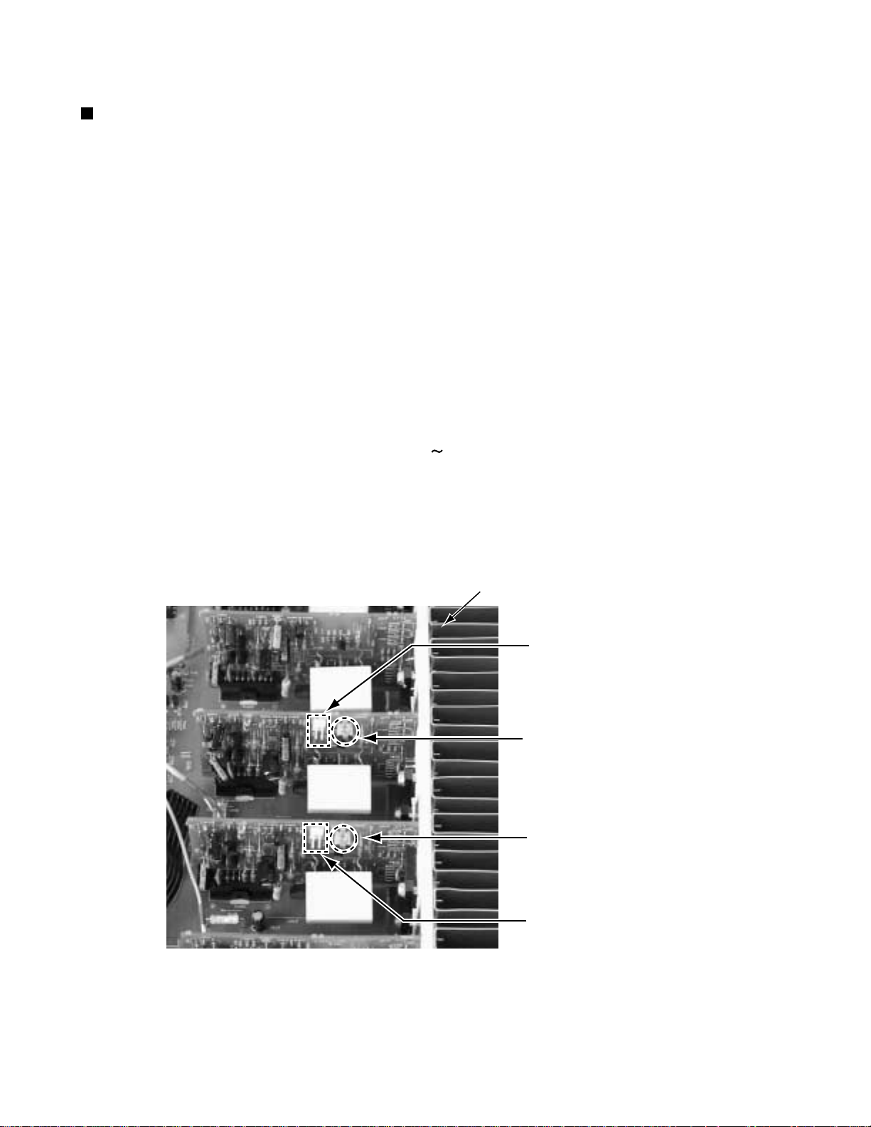
Removing the Heat sink
(See Fig.10 to 11)
1.
Remove the ten screws K and four screws L
attaching the heat sink.
2.
Remove the two screws J attaching the heat sink
from the rear side of main board.
J
Heat sink
L
Main board
rear side
K
Fig.10
K
Fig.11
J
K
L
1-6
Page 7
Removing the power supply board
(See Fig.12)
Prior to performing the following procedure, remove
the top cover.
1.
Disconnect the card wire from connector CN204 on
the power supply board.
2.
Disconnect the harness connected to connector
CN201 and CN707 on the power supply board
(If necessary, cut off the band fixing the harness on
the side of the base chassis).
3.
Disconnect the harness connected to connector
CN206 on the main board
N
CN204
CN707
Hook
CN206
CN201
CN202
RX-E100SL
Power
supply
board
N
PW201
PW203
Solder
PW202
N
M
4.
Remove the three screws N attaching the power
supply board.
5.
Unsolder the three harnesses connected to the
power supply board.
Removing the power transformer
(See Fig.12 and 13)
Prior to performing the following procedures, remove
the top cover.
1.
Disconnect the harness from connector CN217 on
the power / fuse board (If necessary, cut off the tie
band fixing the harness).
2.
Disconnect the harness from connector CN201 and
CN202 on the power supply board and main board.
3.
Remove the four screws M attaching the power
transformer.
Removing the power / fuse board
(See Fig.13)
Prior to performing the following procedure, remove
the top cover and the rear panel.
Power
transformer
Power
transformer
board
CN217
Power cord
Tie band
M
Fig.12
Tie band
O
Solder
Power / fuse board
Fig.13
1.
Disconnect the harness connected to connector
CN217 on the power / fuse board (If necessary, cut
off the band fixing the harness on the side of the
base chassis).
2.
Unsolder the power cord and other harnesses
connected to the power / fuse board.
3.
Remove the screw O attaching the power / fuse
board.
1-7
Page 8

RX-E100SL
Removing the system control board /
power switch board (See Fig.14)
Prior to performing the following procedure, remove
the top cover and the front panel assembly.
1.
Remove the two screws P attaching the power
switch board.
2.
Remove the seven screws Q attaching the system
control board.
Q
System control board
Fig.14
Power switch
board
Q
P
1-8
Page 9
RX-E100SL
Adjustment method
Power amplifier section
Adjustment of idling current
Measurement terminal B451-B452(Lch) , B453-B454(Rch)
Adjustment volume VR301(Lch) , VR302(Rch)
Attention
This adjustment does not obtain a correct adjustment value immediately after the amplifier is
used (state that an internal temperature has risen).
Please adjust immediately after using the amplifier after turning off the power supply of the
amplifier and falling an internal temperature.
<Adjustment method>
1. Prior to turning the power ON, fully turn the adjusting resistor (VR301(Lch),VR302(Rch)) counterclockwise
direction and connect the DC voltmeter to the measuring terminal(B451-B452(Lch) , B453-B454(Rch)).
2. Set the surround mode OFF.
3. Adjust the resistor so that the measured value becomes 2mV immediately after turning the power ON.
4. When the idling current has been stable (about 30 minutes after the power is turned ON),
confirm that the measured value falls within 1.0mV 10mV(2.3mV).
* It is not abnormal though the idling current might not become 0mA even if it is finished to turn variable
resistance (VR301VR302) in the direction of counterclockwise.
Heat sink
B453-B454 (Rch)
VR302 (Rch)
VR301 (Lch)
B451-B452 (Lch)
1-9
Page 10
RX-E100SL
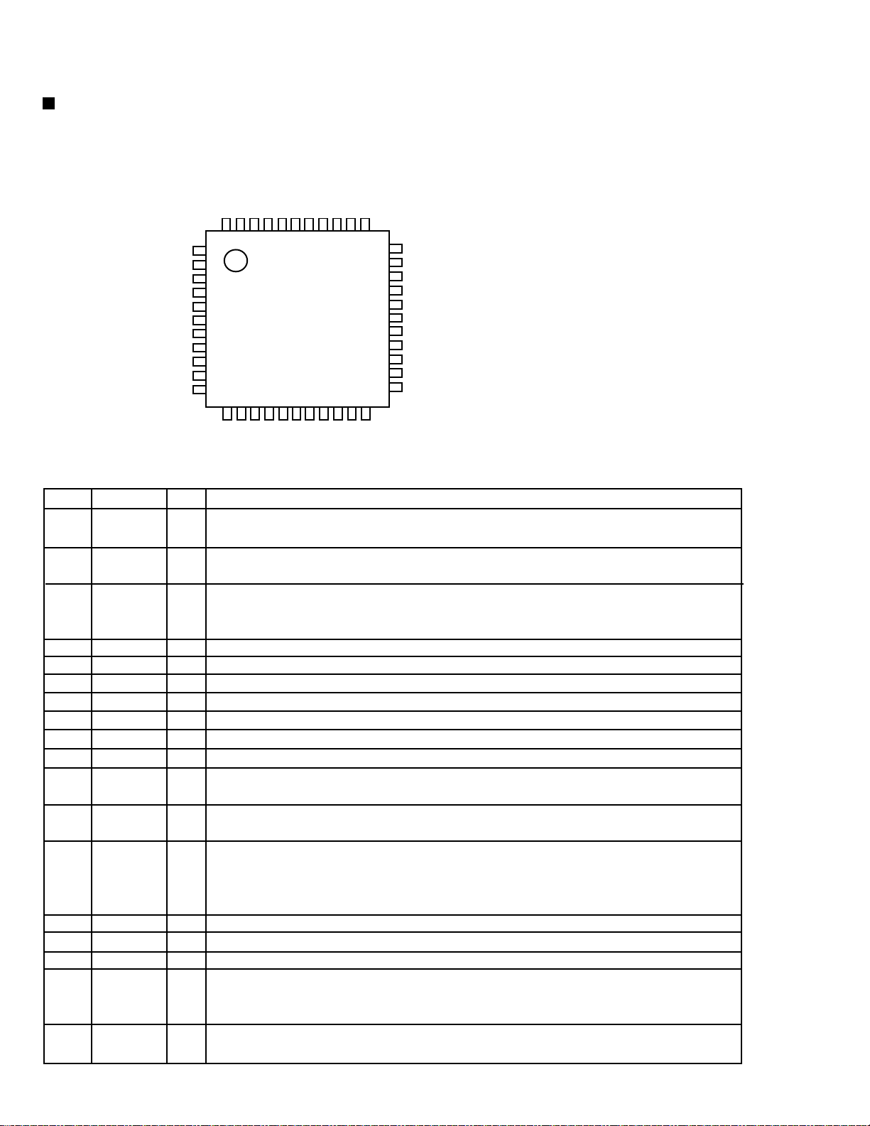
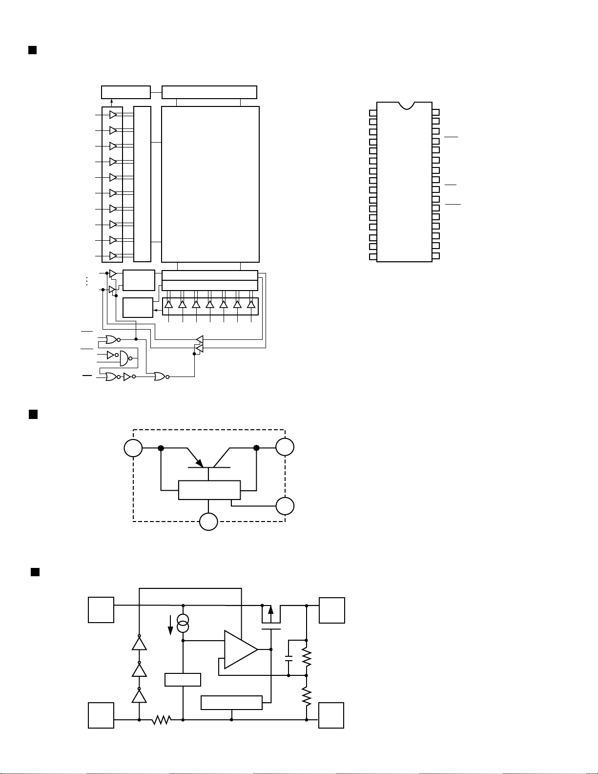
Description of major ICs
AK4527B (IC601) : A/D,D/A Converter
1.Pin layout
LOOP1
LOOP0/SDA/CDTI
DIF1/SCL/CCLK
DIF0/CSN
P/S
MCLK
DZF1
AVSS
AVDD
VREFH
VCOM
SDOS
I2C
SMUTE
BICK
LRCK
SDTI1
SDTI2
SDTI3
SDTO
DAUX
DFS
2. Pin function (1/2)
No.
1
2
3
4
5
6
7
8
9
10
11
12
13
14
15
16
17
18
Pin name
SDOS
I2C
SMUTE
BICK
LRCK
SDTI1
SDTI2
SDTI3
SDTO
DAUX
DFS
NC
DZEF
TVDD
DVDD
DVSS
PDN
TST
4443424140393837363534
1
2
3
4
5
6
7
8
9
10
11
I/O
I
SDTO Source Select Pin (Note 1)
AK4527BVQ
Top View
1213141516171819202122
NC
DZFE
TVDD
DVDD
DVSS
PDN
TSTNCADIF
Function
CAD1
CAD0
33
32
31
30
29
28
27
26
25
24
23
DZF2/OVF
RIN+
RINLIN+
LINROUT1
LOUT1
ROUT2
LOUT2
ROUT3
LOUT3
"L" : Internal ADC output, "H" : DAUX input
I
Control Mode Select Pin
"L" : 3-wire Serial, "H" : I
I
Soft Mute Pin (Note 1)
2
C Bus
When this pin goes to "H", soft mute cycle is initialized.
When returning to "L", the output mute releases.
I
Audio Serial Data Clock Pin
I/O
Input Channel Clock Pin
I
DAC1 Audio Serial Data Input Pin
I
DAC2 Audio Serial Data Input Pin
I
DAC3 Audio Serial Data Input Pin
O
Audio Serial Data Output Pin
I
Sub Audio Serial Data Input Pin
I
Double Speed Sampling Mode Pin (Note 1)
"L" : Normal Speed, "H" : Double Speed
-
No Connect
No internal bonding.
I
Zero Input Detect Enable Pin
"L" : mode 7 (disable) at parallel mode,
zero detect mode is selectable by DZFM2-0 bits at serial mode.
"H" : mode 0 (DZF is AND of all six channels)
-
Output Buffer Power supply Pin, 2.7V~5.5V
-
Digital Power Supply Pin, 4.5V~5.5V
-
De-emphasis Pin, 0V
I
Power-Down & Reset Pin
When "L", the AK4527B is powered-do wn and the control registers are reset to def ault
state. If the state of P/S or CAD0-1 changes, then the AK4527B m ust be reset b y PDN.
I
Test Pin
This pin should be connected to DVSS.
AK4527(1/2)
1-10
Page 11
RX-E100SL
Pin function (2/2)
Pin name
No.
NC
19
ADIF
20
CAD1
21
CAD0
22
LOUT3
23
ROUT3
24
LOUT2
25
ROUT2
26
LOUT1
27
ROUT1
28
LIN-
29
LIN+
30
RIN-
31
RIN+
32
DZF2
33
OVF
VCOM
34
VREFH
35
AVDD
36
AVSS
37
DZF1
38
MCLK
39
P/S
40
DIF0
41
CSN
DIF1
42
SCL/CCLK
LOOP0
43
SAD/CDTI
LOOP1
44
No Connect
I/O
No internal bonding.
-
Function
Analog Input Format Select Pin
"H" : Full-differential input, "L" : Single-ended input
I
Chip Address 1 Pin
Chip Address 0 Pin
I
DAC3 Lch Analog Output Pin
I
DAC3 Rch Analog Output Pin
O
DAC2 Lch Analog Output Pin
O
DAC2 Rch Analog Output Pin
O
DAC1 Lch Analog Output Pin
O
DAC1 Rch Analog Output Pin
O
Lch Analog Negative Input Pin
O
Lch Analog Positive Input Pin
I
Rch Analog Negative Input Pin
I
Rch Analog Positive Input Pin
I
Zero Input Detect 2 Pin (Note 2)
I
When the input data of the group 1 follow total 8192LRCK cycles with "0" input data,
O
this pin goes to "H".
Analog Input Overflow Detect Pin (Note 3)
This pin goes to "H" if the analog input of Lch or Rch is overflows.
O
Common Voltage Output Pin,AVDD/2
Large external capacitor around 2.2uF is used to reduce power-supply noise.
O
Positive Voltage Reference Input Pin,AVDD
Analog Power Supply Pin,4.5V~5.5V
I
Analog Ground Pin,0V
Zero Input Detect 1 Pin (Note 2)
When the input data of the group 1 follow total 8192 LRCK cycles with "0" input data,
O
this pin goes to "H".
Master Clock Input Pin
Parallel / Serial Select Pin
I
"L" : Serial control mode, "H" : Parallel control mode
I
Audio Data Interface Format 0 Pin in parallel mode
Chip select pin in 3-wire serial control mode
I
This pin should be connected to DVDD at I2C bus control mode
I
Audio Data Interface Format 1 Pin in parallel mode
Control Data Clock Pin in serial control mode
I
I2C = "L" : CCLK(3-wire Serial), I2C = "H" : SCL(I2CBus)
I
Loopback Mode 0 Pin in parallel control mode
Enables digital loop-back from ADC to 3 DACs.
I
Control Data Input Pin in serial control mode
I2C = "L" : CDTI(3-wire Serial), I2C = "H" : SDA(I2CBus)
I/O
Loopback Mode 1 Pin (Note 1)
Enable all 3 DAC channels to be input from SDTII.
I
AK4527(1/2)
Notes : 1. SDOS, SMUTE, DFS, and LOOP1 pins are ORed with register data if P/S = "L".
2. The group 1 and 2 can be selected by DZFM2-0 bit if P/S = "L" and DZFME = "L".
3. This pin becomes OVF pin if OVFE bit is set to "1" at serial control mode.
4. All input pins should not be left floating.
1-11
Page 12
RX-E100SL
UPD784215AGC103 (IC671) : UNIT CPU
1.Pin layout
75 ~ 51
76
~
50
~
100
1 ~ 25
26
2.Pin function
Pin No. Symbol I/O Function
1~8
9
10
11
12
13
14
15
16
17
18
19
20
21
22
23
24
25~32
33
34,35
36
37,38
39
40
41
42
43
44
45,46
47
48
49
50
51,52
53
54~63
64,65
66
67
68
69,70
71
72
73~80
81
82
83
84
85
86
87
88
89
90~93
94
95~100
VDD
X2
X1
VSS
XT2
XT1
RESET
AUTODAT A
LOCK
DIGITAL0
FORMAT
CHANNEL
ERR
RSTDET
AVDD
AVREF0
AVSS
AV REF1
RX,TX
DSPCOM
DSPSTS
DSPCLK
DSPRDY
MIDIO_IN/OUT
MICK
MICS
MILP
MIACK
DSPRST
CDTI/CDTO
CCLK
CS
XTS
PD
GND
VDD
3D-ON
3D-ON
ANA/T-TONE
REF-MIX
D.MUTE
S.MUTE
ASW1~4
TEST
Non connect
Power supply terminal
Connecting the crystal oscillator for system main clock
O
Connecting the crystal oscillator for system main clock
I
Connect to GND
Connecting the crystal oscillator for system sub clock
O
Connecting the crystal oscillator for system sub clock
I
System reset signal input
I
Output of DSP to general-purpose port
I
Output of DSP to general-purpose port
I
Output of DSP to general-purpose port
I
Output of DSP to general-purpose port
I
Output of DSP to general-purpose port
I
Output of DSP to general-purpose port
I
Reset signal input
I
Power supply terminal
Connect to GND
Connect to GND
Connect to GND
Non connect
Power supply terminal
Not use
Non connect
Communication port from IC701
I
Status communication port to IC701
O
Clock input from IC701
I
Ready signal input from IC701
I
Non connect
Interface I/O terminal with microcomputer
I/O
Interface I/O terminal with microcomputer of clock signal
O
Interface I/O terminal with microcomputer of chip select
O
Interface I/O termonal with microcomputer
O
Interface I/O termonal with microcomputer
O
Non connect
Reset signal output of DSP
O
Non connect
Interface I/O terminal with microcomputer
I/O
Interface I/O terminal with microcomputer of clock signal
O
Interface I/O terminal with microcomputer of chip select
O
OSC Select
O
Non connect
Reset signal output
O
Connect to GND
Non connect
Power supply
Non connect
Switch at output destination of surround channel
O
Test tone control
O
Control at output destination of LFE channel
O
Non connect
Mute of the digital out terminal is controlled
O
Mute of the audio signal is controlled
O
Non connect
Selection of digital input selector
O
Test terminal
Non connect
-
1-12
Page 13
TC9446F-014 (IC631) : Digital signal processor for dolby digital (AC-3)
/ MPEG2 audio decode
Pin No. Symbol I/O Function
1
2
3
4
5
6
7
8~11
12
13
14
15
16~18
19
20
21
22
23
24
25
26
27,28
29~31
32,33
34
35
36
37
38,39
40
41
42
43
44
45
46
47
48
49
50
51
52
53
54~61
62
63~70
71
72~80
81
82~89
90
91
92,93
94
95
96
97
98,99
100
RST
MIMD
MICS
MILP
MIDIO
MICK
MIACK
FI0~3
IRQ
VSS
LRCKA
BCKA
SDO0~2
SD03
LRCKB
BCKB
SDT0
SDT1
VDD
LRCKOA
BCKOA
TEST0,1
LRCKOB,BCKOB,TXO
TEST2,3
RX
VSS
TSTSUB0
FCONT
TSTSUB1,TSTSUB2
PDO
VDDA
PLON
AMPI
AMPO
CKI
VSSA
CKO
LOCK
VSS
WR
OE
CE
VDD
IO7~0
VSS
AD0~7
VDD
AD8~16
VSS
PO0~7
VDDDL
LPFO
DLON,DLCKS
SCKO
VSSDL
SCKI
VSSX
XO,XI
VDDX
Reset signal input terminal (L:reset H:Operation usually)
I
Microcomputer interface mode selection input terminal (L:serial H:IC bus)
I
Microcomputer interface chip select input terminal
I
Microcomputer interface latch pulse input
I
Microcomputer interface data I/O terminal
I/O
Microcomputer interface clock input terminal
I
Microcomputer interface acknowledge output terminal
O
Flag input terminal 0~3
I
Interrupt input terminal
I
Digital ground terminal
Audio interface LR clock input terminal A
I
Audio interface bit clock input terminal A
I
Audio interface data output terminal 0
O
Non connect
Audio interface LR clock input terminal B
I
Audio interface bit clock input terminal B
I
Audio interface data input terminal 0
I
Audio interface data input terminal 1
I
Power supply for digital circuit
Audio interface LR clock output terminal A
O
Audio interface bit clock output terminal A
O
Test input terminal 0/1 (L:test H:operation usually)
I
Non connect
Test input terminal (L:test H:operation usually)
I
SPDIF input terminal
I
Ground terminal for digital circuit
Test sub input terminal 0 (L:test H:operation usually)
I
VCO Frequency control output terminal
O
Test sub input terminal 1,2 (L:test H:operation usually)
I
Phase error signal output terminal
O
Power supply for analog circuit
Clock selection input terminal (L:external clock H:VCO clock)
I
AMP.input terminal for LPF
I
AMP.output terminal for LPF
O
External clock input terminal
I
Ground terminal for analog circuit
DIR Clock output terminal
O
VCO Lock detection output terminal
O
Ground terminal for digital circuit
External SRAM writing signal output terminal
O
External SRAM output enable signal output terminal
O
External SRAM chip enable signal output terminal
O
Power supply terminal for digital circuit
External SRAM data I/O terminal 7~0
I/O
Ground terminal for digital circuit
External SRAM address output terminal 0~7
O
Power supply terminal for digital circuit
External SRAM address output terminal 8~16
O
Ground terminal for digital circuit
General purpose output terminal 0~7
O
Power supply terminal for DLL
LPF output terminal for DLL
O
Refer to the undermentioned table
I
Non connect
Ground terminal for DLL
External system clock input terminal
I
Ground termonal for oscillation circuit
Oscillation I/O terminal
I/O
Power supply terminal for oscillation circuit
-
RX-E100SL
DLCKS terminal
L
L
H
H
DLONterminal
L
H
L
H
DLL clock setting
SCKI input (DLL circuit OFF)
Four times XI clock
Three times XI clock
Six times XI clock
1-13
Page 14
RX-E100SL
W24L010AJ-12 (IC641) : CMOS SRAM
Block diagram
A16
A14
A12
A4
A3
A2
A7
A6
A5
A9
I/O 1
I/O8
WE
CS1
CS2
R
O
W
D
E
C
O
D
E
R
DATA
CNTRL.
CLK
GEN.
PRECHARGE CKT.CLK GEN.
CORE CELL ARRAY
7024 ROWS
728x8 COLUMN5
I/O CKT
COLUMN DECODER
A15 A13 A8 A1 A0 A11 A10
Pin layout
NC
A16
A14
A12
A7
A6
A5
A4
A3
A2
A1
A0
I/O1
I/O2
I/O3
Vss
1
2
3
4
5
6
7
8
9
10
11
12
13
14
15
16
32
31
30
29
28
27
26
25
24
23
22
21
20
19
18
17
VDD
A15
CS2
WE
A13
A8
A9
A11
OE
A10
CS2
I/O8
I/O7
I/O6
I/O5
I/O4
OE
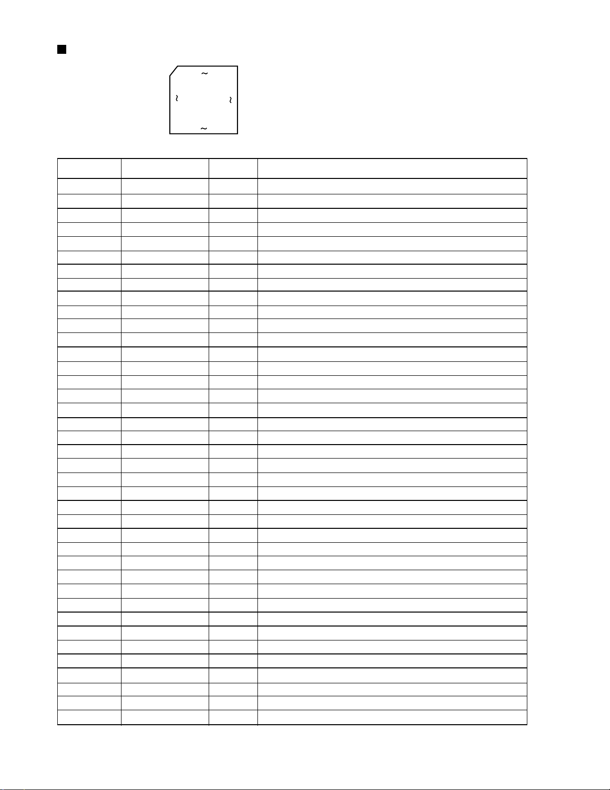
PQ3DZ53 (IC681) : Regulator IC
DC INPUT(Vin)
1
CUSTOM IC
5
GND
RN5RZ33BA (IC683) : Voltage regurator
2
VDD
-
+
3
DC OUTPUT(Vo)
ON/OFF CONTROL(Vc)
2
VOUT
3
1-14
CE
Vref
GND
Current Limit
5
1
Page 15
MN101C35DHR (IC401) : System controller
100 76
1
75
RX-E100SL
Pin function (1/2)
Pin No.
1
2
TXD/SB00/P00
RXD/SBI0/P01
3
4
5
6
7
8
9,10
11
12
13
14
15
16
17
18
19
20
21
22
23
24
25
26
27
28
29
30
31
32
33
34
SENS/IRQ1/P21
35
36
37
38
39
40
25
26 50
Symbol
SBT0/P02
SB01/P03
SBI1/P04
SBT1/P05
BUZZER/P06
VDD
OSC1,2
VSS
XI
X0
MMOD
VREFAN0/PA0
AN1/PA1
AN2/PA2
AN3/PA3
AN4/PA4
AN5/PA5
AN6/PA6
AN7/PA7
VREF+
P07
RST /P27
TM0IO/P10
TM1IO/P11
TM2IO/P12
TM3IO/P13
TM4IO/P14
P15
IRQ0/P20
IRQ2/P22
IRQ3/P23
IRQ4/P24
P25
SB02/P30
SBI2/P31
51
I/O
-
I
-
I
-
-
I/O
-
-
O
-
I
I
I
I
I
-
-
-
-
I
O
I
O
I
O
I/O
I
I
I
I
I
O
I
Function
GND
GND
PROTECTOR INPUT
GND
GND
GND (TV LINK INPUT)
NC
POWER SUPPLY +5V
OSC (8MHz)
GND
GND
OPEN
GND
GND
KEY INPUT 1 (7KEY)
KEY INPUT 2 (7KEY)
KEY INPUT 3 (7KEY)
CHIP SELECT 1
CHIP SELECT 2
NC
NC
NC
POWER SUPPLY +5V
NC
RESET INPUT
RDS SDA IN/OUT
RDS SCL IN/OUT
TUNER CE
TUNER MUTE
TUNER CLK
TUNER DATA IN/OUT
GND
REMOCON INPUT
INH INPUT
RDS DAVN INPUT
TUNED INPUT
STEREO INPUT
DSP MICON COMMAND
DSP MICON STATUS
1-15
Page 16
RX-E100SL
Pin function (2/2)
Pin No.
41
42
43
44
45
46
47
50
51
54
55
56
57
63
64
65
72
73
88
89
90
91
92
93
94
95
96
97
98
99
100
Symbol
SBT2/P32
P50
P51
P52
P53
P54
DGT17/P67
DGT14/P64
DGT13/P63
DGT10/P60
DGT9/P41
DGT8/P40
SEG0/DGT7/P77
SEG6/DGT1/P71
SEG7/DGY0/P7
SEG8/P87
SEG15/P80
SEG16/P97
SEG31/PB3
SEG32/PB2
SEG33/PB1
SEG34/PB0
SEG35/PD7
SEG36/PD6
SEG37/PD5
SEG38/PD4
SEG39/PD3
SEG40/PD2
SEG41/PD1
SEG42/PD0
VPP
I/O
O
O
O
O
O
O
-
O
O
O
O
O
O
O
O
-
-
O
O
O
O
O
O
O
O
Function
DSP MICON CLK
DSP MICON READY
DSP MICON RESET
M61501 CLK
M61501 DATA
M61501 LATCH
NC
GRID 1
GRID 4
GRID 5
GRID 6
GRID 7
GRID 13
SEGMENT 17
SEGMENT 18
SEGMENT 25
SEGMENT 1
SEGMENT 16
STANDBY LED
NC
NC
NC
FRONT SPK RELAY
CENTER SPK RELAY
REAR SPK RELAY
POWER ON
SWITCH MODE ON
SUBWFR MUTE
SOURCE MUTE
VPP
1-16
Page 17
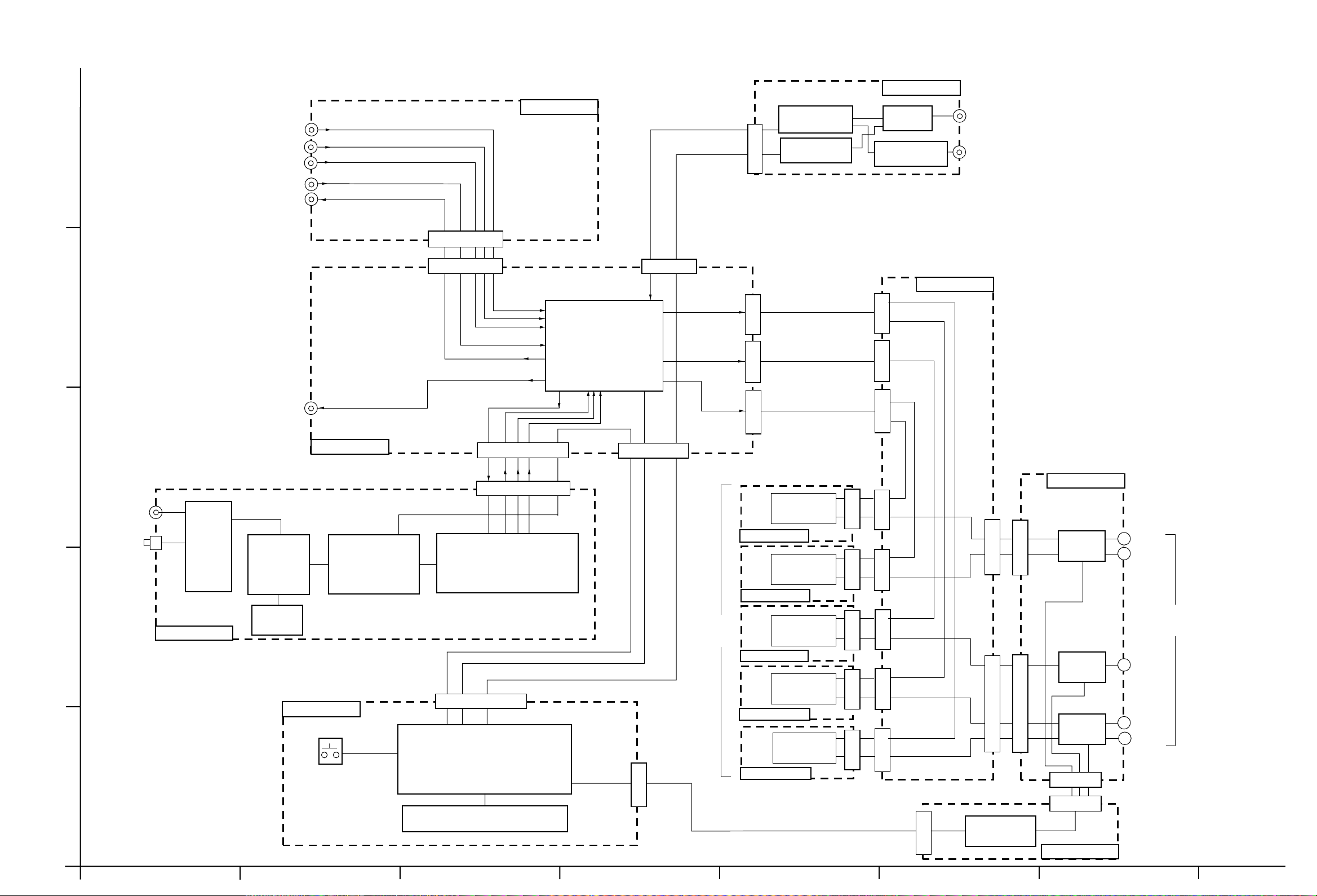
RX-E100SL
Block diagram
5
4
DVD
TV
CD
VCR PLAY
VCR REC
SUBWOOFER
OUT
DVD AUDIO IN
TV AUDIO IN
CD AUDIO IN
CN522
CN502
VCR PLAY
VCR REC
SUBWOOFER OUT
LVA10229-6
AUDIO SW
IC501
&
VOLUME
TUNER L/R
CN503
PLL CLK,
PLL DATA, PLLCE
REAR
CENTER
FRONT
CN111
CN506CN505 CN507
AM/FM DET
IC102
PLL
IC121
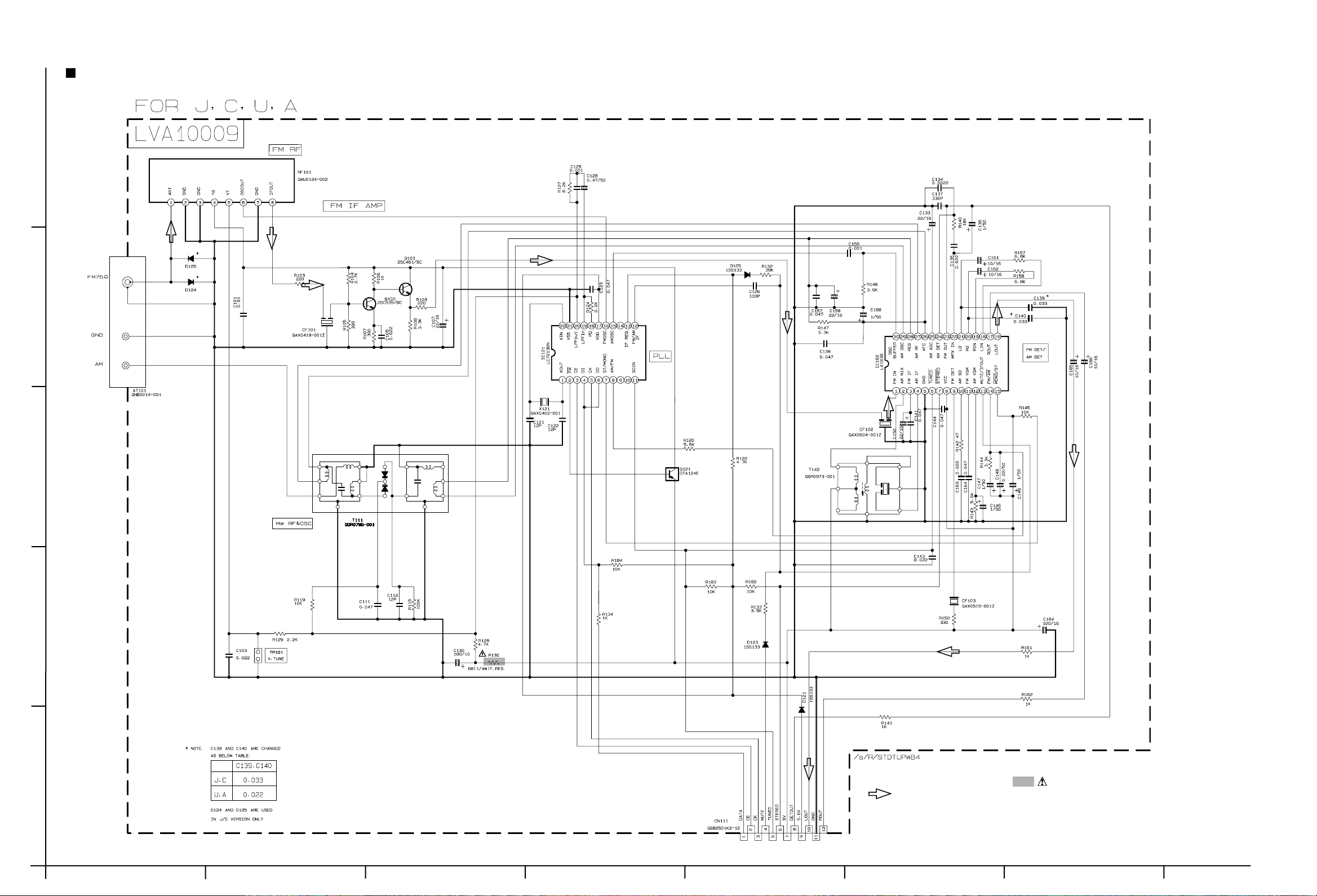
LVA10009-1
TUNER
RF101
MW RF&OSC
T111
LVA10229-2
CN517
CN516CN515CN711
FM
AM
3
2
1
COAXIAL
IN
OPTICAL
IN
SW
IC611
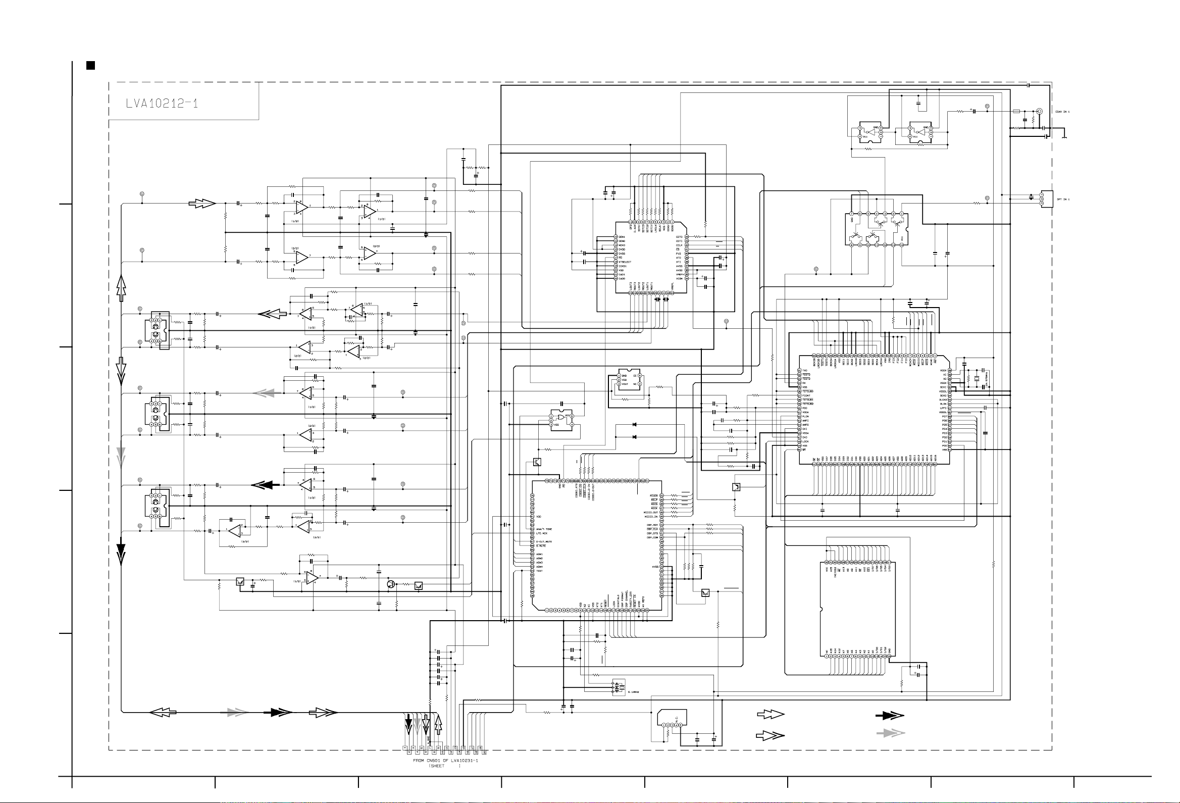
LVA10212-1
DSP
IC631
SDRAM
IC641
LVA10231-1
CONTROLLER
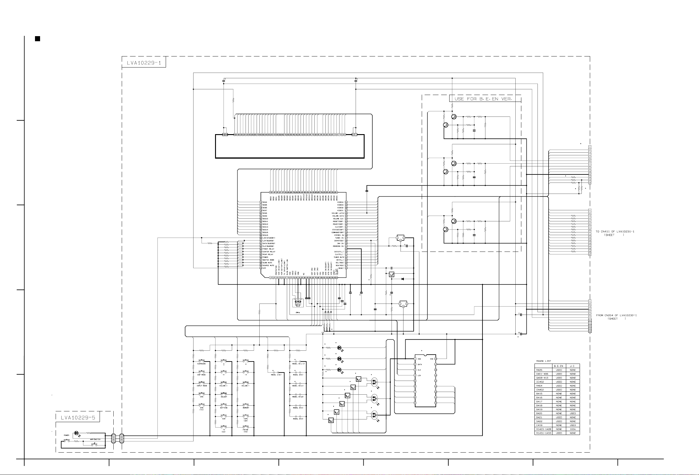
LVA10229-1
CN501
CN681
DSP
AD/DA CONVERTER
IC671
DSP COMMAND, DSP CLK, DSP STATUS, DSP READY, DSP RESET
IC601
VOLCLK, VOLD ATA, VOL LATCH
CN401
KEY
SYSTEM CONTROLLER
IC401
FL DISPLAY
DI401
RY HP, RY LR1
RY LR2, RY C
CN411
CN214
PLL CLK, PLL DATA, PLLCE,
AUDIO
AMP.
Lch
LVA10230-4
Rch
LVA10230-5
Cch
LVA10230-8
RLch
LVA10230-6
RRch
LVA10230-7
Q315
Q317
Q316
Q318
Q915
Q917
Q815
Q817
Q816
Q818
CN701CN702CN705CN703CN704
CN712
CN715
CN713
CN714
CN204
FW701
FW702
Q207~Q209
FW701
FW702
LVA10229-3
RY741
RY743
RY742
FW707
CN707
LVA10230-1
Lch
Rch
SPEAKER
TERMINAL
Cch
RLch
RRch
ABCD E F G
2-1
Page 18
Standard schematic diagrams
Power supply section
5
RX-E100SL
2 / 7
POWER
CN217
PW101
PW103
PW102
D212
1SR35
R205
3.3M
F201
5A-125V
R213
330
C213
2200/6.3
TA201
TA202
EP201
EP202
SHEET
NUMBER
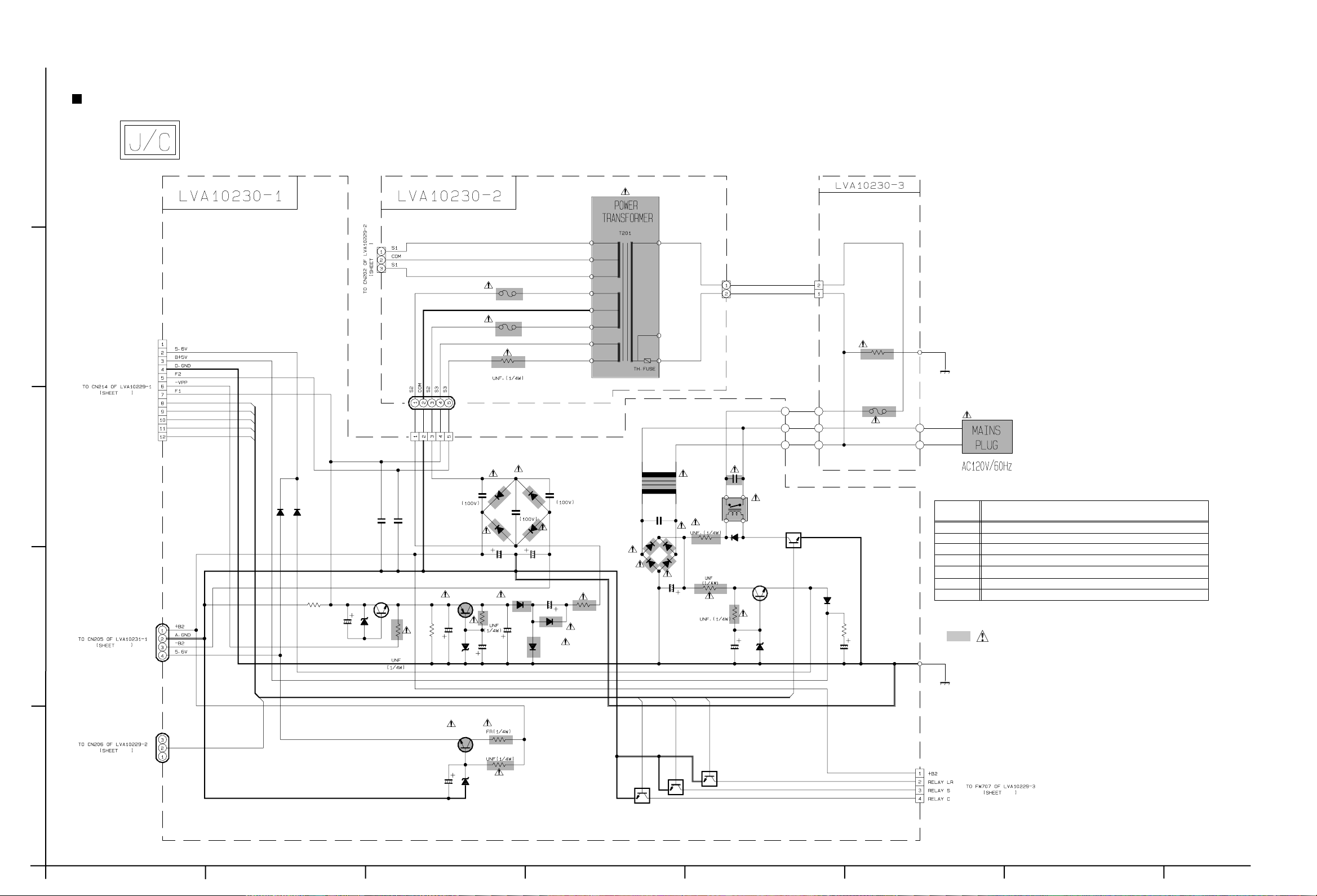
1 / 7 POWER SUPPLY
2 / 7 SPEAKER TERMINAL & VIDEO/AUDIO SIGNAL INPUT TERMINAL
3 / 7 AUDIO AMP
4 / 7 AUDIO SIGNAL INPUT TERMINAL
5 / 7 SYSTEM CONTROL & FL DISPLAY
6 / 7 DSP
7 / 7 TUNER
CIRCUIT DESCRIPTION
Parts are safety assurance parts.
When replacing those parts make
sure to use the specified.
FW202
4
5 / 7
POWER
RELAY_LR
RELAY_C
RELAY_S
PROTECTOR
CN204
FW201
CN201
3
C202
0.1
D219
1SR35
1SR35
R209
100k
C218
1/50
C206
0.047
D217
MTZJ6.2C
R208
10
C207
0.047
22k
R207
C217
Q204Q205
KTA1046/YKTC3200/GL
22/50
D216
MTZJ33C
D220
2
4 / 7
FW205
F202
2A-125V
F203
2A-125V
R201
5.6
D201
10E2-FD
D203
10E2-FD
C204 C205
2200/35
1SR35-400A
R206
3.3k
C216
22/50
D202
1SR35-400A
C201
0.1
1000/35
D215
C215
100/63
1SR35-400A
1SR35-400A
C203
0.1
D204
1SR35-400A
C214
220/50
D213
D214
TH201
QAD0095-4R7
C208
0.0047/100
D207
1SR35-400A
D206
1SR35-400A
D208
1SR35-400A
C209
470/25
CN207
T202
QQT0317-001
R202
10
R203
10
D209
1SR35-400A
R204
470/16
820
C212
D210
1SS133
PW201
PW203
PW202
C210
0.0047
RY201
QSK0055-001
Q203
KTC3203/OY
D211
MTZJ6.2C
Q202
KRC105M
R211
FW206
2 / 7
1
PROTECTOR
100/25 MTZJ6.2C
Q211
2SD2395/EF
C221 D221
12
R212
6.8k
RELAY_C
Q209
KRC105M
RELAY_S
Q208
KRC105M
RELAY_LR
Q207
KRC105M
CN707
2 / 7
SHEET 1/7
2-2
HABC DEFG
Page 19
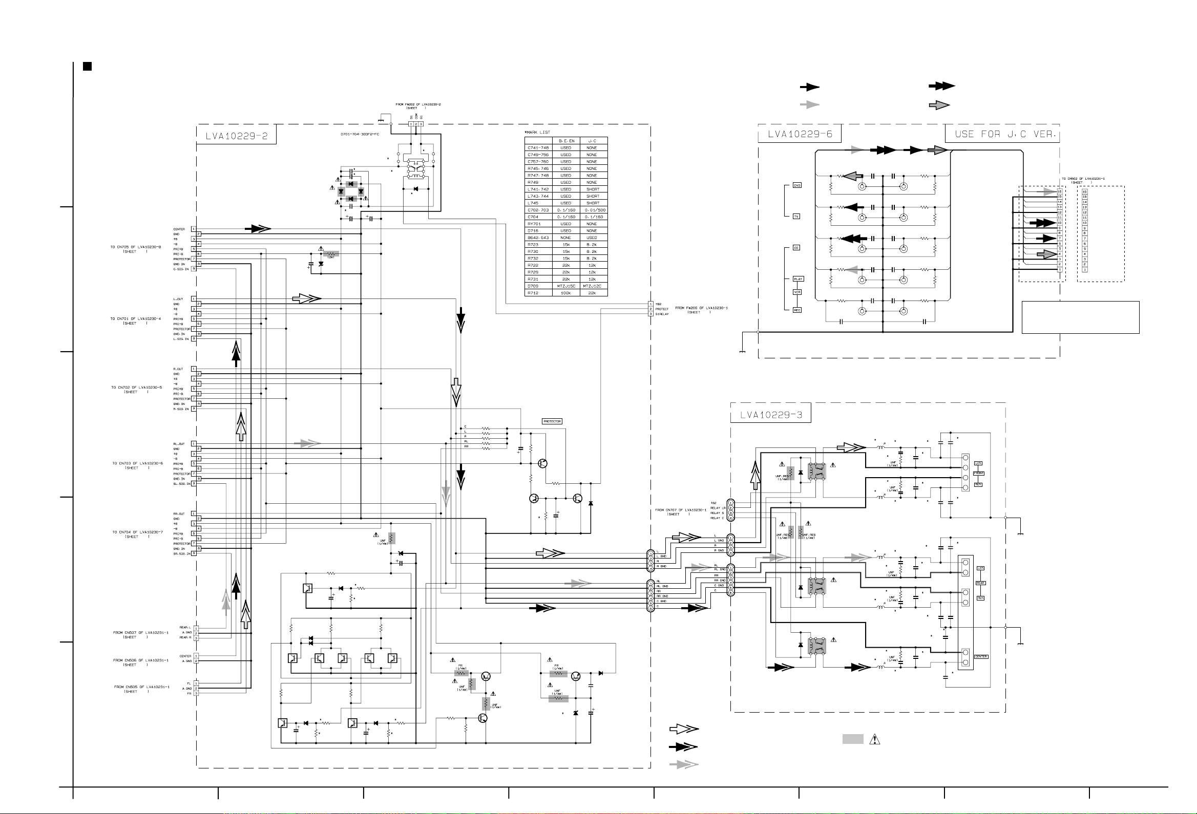
Speaker terminal & Video / Audio input terminal section
RX-E100SL
TV Audio signal
1 / 7
D716
1SS133
CN202
B643
J1582
J1581
CN206
1 / 7
EP701
5
B643
C701
C702
D701
D702
D704
C703
R701
5.6k
D705
MTZJ18C
C704 C705
4700/63 4700/63
CN715
3 / 7
C706
47/25
D703
RY701
QSK0082-001
4
CN711
3 / 7
CN712
VCR Audio signal
C1581 C1582
DVD_L
TV_L
CD_L
VCR-L
VCR_LOUT
R1591
100k
R1583
R1593
100k
R1585
R1595
100k
R1587
R1597
100k
R1589
470
470
470
470
XX
C1583 C1584
XX
C1585 C1586
XX
C1587 C1588
XX
C1591 C1592
XX
R1582R1581
470470
R1584
470
R1586
470
R1588
470
R1590
470
C1590C1589
220p220p
R1592
100k
R1594
100k
R1596
100k
R1598
100k
CD signal
DVD Audio signal
DVD_R
TV_R
CD_R
VCR_R
VCR_ROUT
CN522
4 / 7
VCR_L
VCR_R
GND
VCR_ROUT
VCR_LOUT
GND
CD_L
CD_R
GND
TV_L
TV_R
GND
DVD_L
GND
DVD_R
GND
VCR_L
VCR_R
VCR_ROUT
VCR_LOUT
TV_L
TV_R
DVD_L
DVD_R
CN522
Type 1. Type 2.
Note :
There are two types of
connectors in the CN522
3 / 7
R704
3
CN713
3 / 7
CN714
3 / 7
R720
3.9k
D710
MTZ5.1JC
2
R721
4.7k
D711
1SS133
Q708
KRC109M
CN517
4 / 7
CN516
4 / 7
CN515
4 / 7
1
R724
4.7k
D712
1SS133
D713
1SS133
Q710 Q712
KRC109M KRC109M
Q709
KRC109M
Q714
D714 D715
KRC109M
1SS133 1SS133
R729
C714
4.7/50
R730
R722
C713
R723
4.7/50
R725 R726
4.7k 4.7k
Q711 Q713
KRC109M KRC109M
R728R727
4.7k4.7k
Q715
KRC109M
C715
4.7/50
R732
C712
4.7/50
R731
R718
R715
10
R716
22k
100k
R705
100k
R706
82k
R707
100k
R708
82k
C709 R709
10/50 10k
Q702
R712
KTC3200/GL/
R710
KTC3199/GL/
C710
47/16
R713
10
R714
10k
Q704
D709
D707
1SS133
FW701
FW702
Q705Q706
D708
2SD2395/EFKTA1023/OY/
1SS133
C717
100p
C711
22/50
1 / 7
FW707
FW701
FW702
FRONT signal
R711
100k 10k
Q703
KTA1268/GL
1k
R717
22k
Q707
KTC3200/GL
R719
47k
D741
1SS133
R741 RY741
12 QSK0109-001
R742 R743
12 12
RY742
QSK0109-001
D742
1SS133
D743
1SS133
RY743
QSK0109-001
CENTER signal
SURROUND signal
L741
C741
0.45
0.022
R745
3.9
R746
3.9
L742
0.45
C742
0.022
C749
L743
0.45
0.022
R747
3.9
R748
3.9
L744
0.45
C750
0.022
R749
3.9
L745
0.45
C757
0.047
C745 C747
220p 0.022
C743
220p
C744
220p
C746 C748
220p 0.022
C753 C755
220p 220p
C751
220p
C752
220p
C754
220p
C760
220p
C758
220p
C756
220p
C759
220p
ST741
ST742
Parts are safety assurance parts.
When replacing those parts make
sure to use the specified.
SHEET 2/7
ABCD E F G
2-3
Page 20
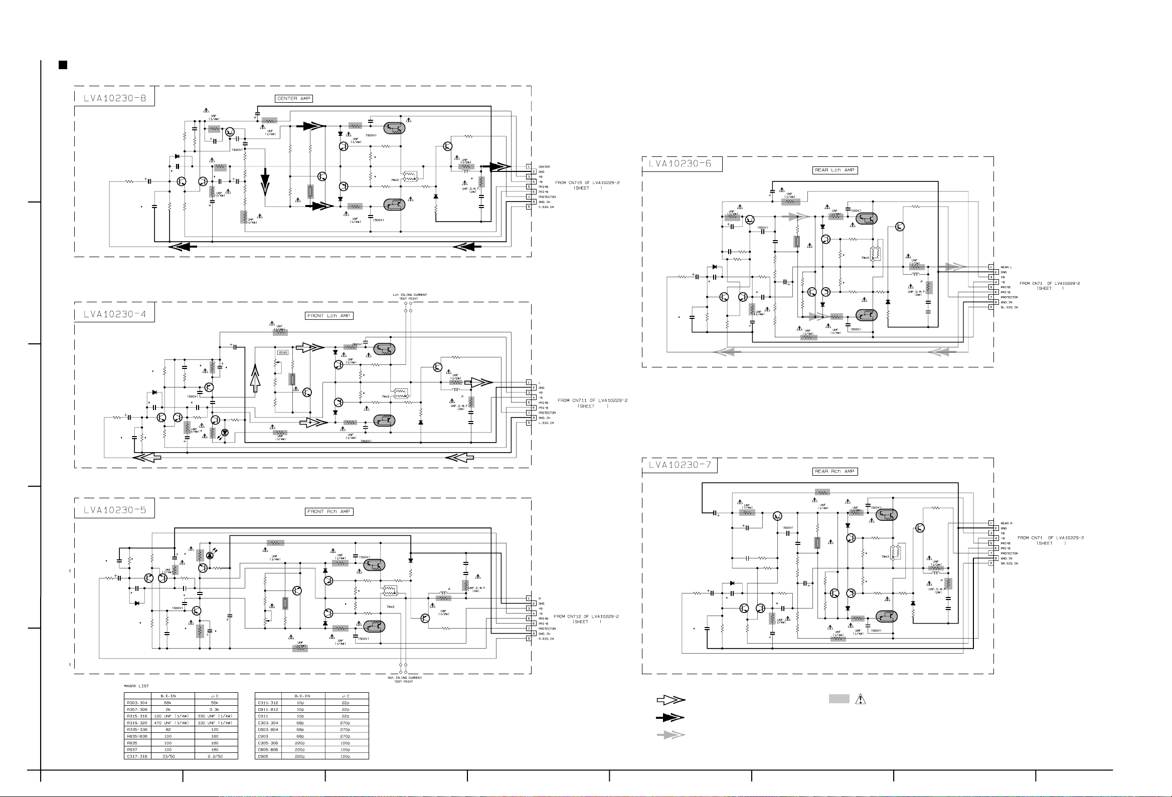
Audio amp section
RX-E100SL
R915
220
C907
0.0015
R907
3k
1002SC2240/BL
R903
R909Q901
R905
C917
2.2/50
Q903
2SC2240/BL
18k
D901
1SS133
C905
56k
5
C901
R901
2.2/50
2.2k
C903
4
C307
R315
R305
12K
Q303
2SC22440/BL
C309
100/16
R309
0.0015
100
C315
22p
R311
390
KTA1268/GL
R313
C311
56k
R319
R307
D301
1SS133
C305
C301
R301
2.2/50
3
2.2k
C303 R303
Q301
2SC22440/BL
Q905
KTA1268/GL
R913
56k
C911
R911
390
C909
47/16
Q305
C313
0.01MY
Q307
KTC3200/GL
D303
SLR-342MC
C317
C915
C319
100/63
R317
47k
33p
R955
3.3k
R957
3.3k
C929
47/50
C919
10/100
R959
3.3k
R961
3.3k
R923
C913
0.01
10
VR301
R921
1K
R939
180
R941
180
R343
0.22
R943
0.22
B452 B451
R345
Q915
2SD2389LD/OPY
R945
1k
Q917
2SB1559LD/OPY
KTA1268/GL
1k
R347
15k
D309
1SS133
Q319
D909
1SS133
R947
18k
Q919
KTA1268/GL
R951
33
L901
0.45
R349
47k
R351
33
L301
0.45
R353
10
R949
47k
R953
10
C925
0.047MY
C927
0.047MY
C325
0.047MY
C327
0.047MY
CN705
CN701
2 / 7
2 / 7
R801
2.2k
C803
C801
2.2/50
R803
56k
D801
1SS133
C805
Q801
2SC2240/BL
2.2/50
C807
0.0015
R815
220
C817
R805
18k
R807
3k
Q805
KTA1268/GL
R809
100
Q803
2SC2240/BL
R811
47/16
390
C809
C819
10/100
C815
33p
0.01MY
R813
56k
C811
C813
R855
3.3k
R857
3.3k
R859
3.3k
R861
3.3k
47/50
C829
R821
10
R829
R831
C821
47p
10
D805
TH801
QAD0012-202
R827
750
360
R825
R823
10
1SS133
2SD637( Q,R)
KTA1268/GL
Q809
D807
1SS133
470
Q811
KTC3200/GL
Q813
R833
10
Q815
2SD2389LD/OPY
R839
180
R843
0.22
R835
R837
R841
180
Q817
2SB1559LD/OPY
C823
47p
R845
1k
D809
1SS133
R847
18k
R849
12k
Q819
KTA1268/GL
R851
33
L801
0.45
R853
10
C825
0.047MY
C827
0.047MY
CN703
3
2 / 7
10
R927
750
R925
360
R321
10
R329
470
R327
TH301
470
R325
360
R323
10
R929
470
TH901
QAD0012-202
QAD0012-202
Q309
D905
1SS133
Q909
2SD637( Q,R)
D907
1SS133
D305
1SS133
2SD637( Q,R)
Q911
KTC3200/GL
Q913
KTA1268/GL
R331
10
Q311
KTC3200/GL
Q313
KTA1268/GL
D307
1SS133
R333
10
R931
R933
10
10
C321
47p
C921
47p
R935
R937
C923
47p
Q315
2SD2389LD/OPY
R339
180
R335
R337
R341
180
Q317
2SB1559LD/OPY
C323
47p
C830
47/50
R860
3.3k
R862
3.3k
R830
470
R822
10
TH802
QAD0012-202
R828
750
R826
360
R824
10
R832
C822
47p
10
D806
1SS133
KTC3200/GL
2SD637( Q,R)
Q814
KTA1268/GL
Q810
D808
1SS133
R834
10
Q812
Q816
2SD2389LD/OPY
R840
180
R844
R836
0.22
R838
R842
180
Q818
2SB1559LD/OPY
C824
47p
R846
1k
D810
1SS133
R848
18k
R850
12k
Q820
KTA1268/GL
R852
33
L802
0.45
R854
10
C826
0.047MY
C828
0.047MY
Parts are safety assurance parts.
When replacing those parts make
sure to use the specified.
CN704
4
2 / 7
R816
D802
1SS133
C806
Q802
2SC2240/BL
R804
56k
220
C818
2.2/50
C808
0.0015
R806
18k
R810
100
KTA1268/GL
R808
3k
Q804
2SC2240/BL
Q806
47/16
R812
C810
C816
33p
C814
0.01MY
R856
3.3k
R858
3.3k
R814
56k
C812
390
C820
10/100
D304
C316
C308
SLR-342MC
R320
R318
47k
Q308
R314
56k
KTC3200/GL
C314
C312C306
0.01MY
22p
R316
Q306
KTA1268/GL
C318
C320
100/63
R326
R328
R324
10
360
TH302
QAD0012-202
4701K
R322
Q310
10
470
R330VR302
2SD637( Q,R)
D306
1SS133
R334
10
D308
1SS133
Q314
KTA1268/GL
Q312
KTC3200/GL
R332
10
C324
2SB1559LD/OPY
R338
R336
Q316
2SD2389LD/OPY
C322
47P
47P
Q318
R342
180
R340
180
D310
1SS133
R346
1k
R344
0.22
B454 B453
R348
15k
Q320
KTA1268/GL
L302
0.45
R352
33
R350
C328
0.047MY
C326
0.047MY
R354
10
47k
CN702
2 / 7
R802
2.2k
C804
C802
2.2/50
FRONT signal
2
C310
R306
R304
12K
Q302
2SC2240/BL
D302
1SS133
R308
100/16
R312
390
Q304
2SC2240/BL
R310
100
0.0015
R302
2.2k
C304
C302
2.2/50
1
CENTER signal
SURROUND signal
SHEET 3/7
2-4
HABC DEFG
Page 21
RX-E100SL
Audio signal input terminal section
6 / 7
C604
C602
C606
C605
C603
C601
R535
5
R536
10k
10k
DSP_LFE
DSP_C
DSP_SR
DSP_SL
DSP_R
DSP_L
4.7k
R534
DSP_ROUT
4.7k
R533
DSP_LOUT
A+5V
+12V
-12V
DSP_RESET
DSP_READY
DSP_COMMAND
CN601
CN511
CN501
DSP_STATUS
DSP_CLK
4
R1619
100k
C523
0.068MY
DSP_L
DSP_LOUTDSP_ROUT
C519
C522
10/50
VCR_ROUT VCR_LOUT
4.7/50
C520
10/50
C521
4.7/50
DSP_R
0.0068MY
C525
0.0068MY
C526
C524
0.068MY
R1617
100k
TUNER_L
CD_L
TV_L
DVD_L
VCR_L
AVDD
VCR_R
DVD_R
3
C535
0.022
TV_R
CD_R
TUNER_R
R1618
100k
0.0068MY
C527
IC501
M61501FP
C530 C529
0.0068MY
C528
4.7/50 4.7/50
R537
10k
C532
R1620
100k
0.1MY
0.1MY
C531
L_OUT
R_OUT
R538
10k
0.1MY
C533
DSP_SL
C534
0.1MY
DSP_SR
SL_OUT
SR_OUT
SW_OUT
R579
DSP_C
DSP_LFE
68
2
Note : There are two types of connectors in the CN522
Type 2.
Type 1.
VOL_LATCH VOL_LATCH
VOL_DATA
VOL_CLK
C537
0.022
C536
0.022
C556
0.022
R580
68
0.022
C555
VCR_L
VCR_L
VCR_R
C544
4.7/50
GND
VCR_R
R552
100k
GND
VCR_LOUT
VCR_ROUT
VCR_ROUT
VCR_LOUT
R556
BA15218F( 1/2)
TV_L
CD_L
TV_R
CD_R
DVD_L
GND
GND
GND
CD_L
CD_R
1k
IC503
TV_L
R554
27k
TV_R
DVD_L
DVD_R
DVD_R
C549
4.7/50
C550
4.7/50
C545
4.7/50
C546
4.7/50
C541
4.7/50
C542
4.7/50
GND
R569
100k
R570
100k
R557
100k
R558
100k
R545
100k
R546
100k
CN502
CN502
R571
1k
2SC3576
2SC3576
R572
1k
R559
1k
2SC3576
R547
1k
2SC3576
2SC3576
R548
1k
Q505
Q506
Q503
Q501
Q502
R576
4.7k
2 / 7
R575
R573
R574
R561
R549
R550
10k
10k
10k
4.7k
10k
10k
1SS355
D509
C552
0.0056MY
C551
0.0056MY
QQR0590-001
QQR0590-001
FL501
FL502
C553
470/6.3
Q509
DTA114YKA
TV Audio signal
VCR Audio signal
DVD Audio signal
SUB WOOFER signal
R578
CN503
CN411
1k
R577
PLL_DATA
PLL_CE
PLL_CLK
TU_MUTE
TUNED
STEREO
+5.6V
TUNER_L
TUNER_R
22
TUNED
STEREO
PLL_CE
C554
2.2/50
TU_MUTE
PLL_CLK
PLL_DATA
DSP_COMMAND
DSP_STATUS
DSP_CLK
DSP_READY
DSP_RESET
VOL_CLK
VOL_DATA
FRONT signal
CENTER signal
SURROUND signal
DSP signal
CD signal
TUNER signal
CN513
( SEET 7 / 7 )
CN121
S_MUTE
5 / 7
Parts are safety assurance parts.
When replacing those parts make
sure to use the specified.
CN507
2 / 7
CN506
2 / 7
CN505
2 / 7
R541
R583R581
1010
Q510 Q512
KTA1271/OY KTA1046/Y
R582
R529 R530
J504
Q507
2SC3576
1
C563
1.5ML
1k 1k
Q508
2SC3576
R532R531
Q516
DTA114YKA
R1621
C581
2.2/50
1k
10k10k
MTZJ7.5C 100/25100/25100/2547/2547/2547/25
SW_MUTE
D503 C562C561C560C559C558C557
2.2k
Q511
KTC3203/OY
R584
2.2k
EP502
R585
R586
1.8K
10
Q513
2SD2395/EF
R587
4.7
R594
R588
1.8k
R589
Q514
12
2SD2395/EF
4.7
R590
6.8k
D507D506D505D504
MTZJ5.6CMTZJ13CMTZJ13CMTZJ7.5C
+5.6V
2.2
R542
2.2
+B2
-B2
GND
CN205
1 / 7
ABCD E F G
Q515
2SD2395/EF
Q520
2SD2395/EF
D508
MTZJ10C
R591
4.7
R592
4.7
R593
2.7k
R595
R596
0.022
10
C564
1k
Q518
KTC3203/OY
D519
MTZJ10C
C565
100/25
SHEET 4/7
2-5
Page 22
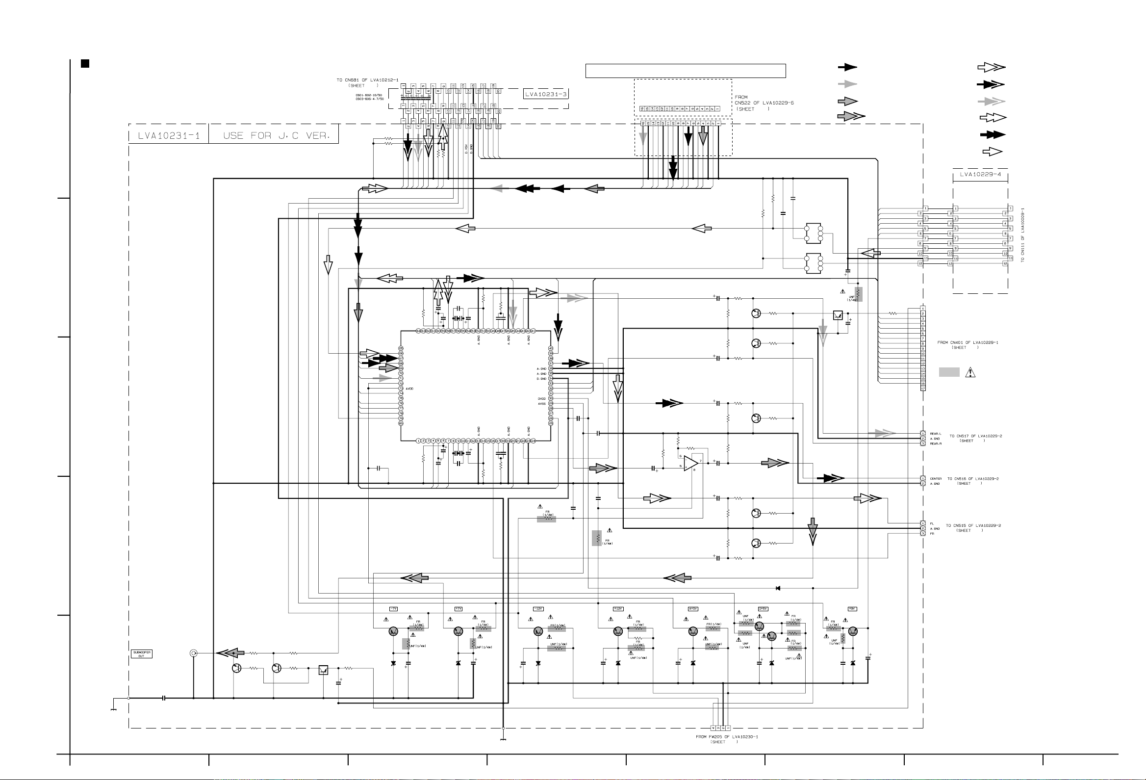
RX-E100SL
System control & FL displaying section
C407C408
SEG24
SEG25
4.7/504.7/50
VIDEO4
VIDEO3
VIDEO2
VIDEO1
VOL_LATCH
VOL_DATA
VOL_CLK
DSP_RESET
DSP_READY
DSP_CLK
DSP_STATUS
DSP_COMMAND
STEREO
TUNED
RDS_DAVN
PLL_DATA
PLL_CLK
TU_MUTE
PLL_CE
RDS_SCL
RDS_SDA
C417
560p
R1426
C402
0.022
GP1U281X
R425
10k
Q407
DTC114EKA
IC403
D408
1SS355
C401
100/6.3
DVD_IN
Q402
KTC3199/GL
STB_IN
Q404
KTC3199/GL
VCR_IN
Q406
KTC3199/GL
R408
R416
R424
R407
10k
Q401
KTC3199/GL
10k
R406
27k
R415
10k
Q403
KTC3199/GL
10k
R414
27k
R423
10k
Q405
KTC3199/GL
10k
R405
R413
R421R422
15k27k
R402R403
47k68k
R404
47k
15k
R412
47k
15k
R420
47k
1000p
C410
1000p
C411
1000p
C409
R401
22k
R464
R465
R466
R467
R468
R469
R470
R471
R472
R473
R474
R475
R476
R477
R478
R479
R480
220
220
220
220
220
220
220
220
220
220
220
220
220
220
220
220
220
R1427
CN402
R1428
CN401
4 / 7
VIDEO1
VIDEO2
VIDEO3
VIDEO4
R410R411
47k68k
R409
22k
R418R419
47k68k
R417
22k
DVD_SLOW
STB_SLOW
VCR_SLOW
TV_OUT
SLOW_L
RDS_DAVN
RDS_SDA
RDS_SCL
SW_MUTE
S_MUTE
TUNED
STEREO
PLL_CE
TU_MUTE
PLL_CLK
PLL_DATA
DSP_COMMAND
DSP_STATUS
DSP_CLK
DSP_READY
DSP_RESET
VOL_CLK
VOL_DATA
VOL_LATCH
SWITCH
5
100k
R1422
SEG16
SEG15
SEG14
SEG13
SEG12
SEG11
SEG10
SEG9
SEG8
SEG7
SEG6
SEG5
SEG4
SEG3
SEG2
SEG1
GRID1
DI401
QLF0086-001
GRID2
GRID3
GRID4
GRID5
GRID6
GRID7
GRID8
GRID9
GRID10
GRID11
GRID12
GRID13
SEG17
SEG18
SEG19
SEG20
SEG21
SEG22
SEG23
4
SEG3
SEG2
SEG1
SEG25
SEG24
SEG23
SEG22
SEG21
SEG20
SEG19
SEG18
SEG17
GRID13
GRID12
GRID11
GRID10
GRID9
GRID8
GRID7
GRID6
GRID5
GRID4
GRID3
GRID2
GRID1
SEG4
SEG5
SEG6
SEG7
SEG8
SEG9
SEG10
SEG11
SEG12
SEG13
SEG14
SEG15
SEG16
R400
10k
R489
R490
R493
R494
R495
R496
R497
R498
R499
10k
10k
10k
10k
10k
10k
10k
10k
10k
R455
3
10k
2092_LCK
2092_DATA
2092_CLK
RELAY_LR
RELAY_C
RELAY_S
POWER
SWITCH
SW_MUTE
S_MUTE
IC401
MN101C35DHR
R426
0.022
C418
C403
22k
2.2/50
IC404
IC-PST9139
R427
4.7k
IC402
BU2092
2092_DATA
2092_CLK
2092_LCK
DVD_R_IND
STB_R_IND
STB_G_IND
VCR_R_IND VCR_G_IND
AM/FM_INDDVD_G_IND
TAPE_IND
TV_IND
C406
4.7/50
C419
100/6.3
SWITCH
+5.6V
B+5V
D.GND
F2
-VPP
F1
POWER
RELAY_LR
RELAY_C
RELAY_S
PROTECTOR
CN214
1 / 7
C405 C404
TV_OUT
C414
C415
0.01
D401
SLR-342MC
D402
SLR-342MC
D403
SLR-342MC
Q411
DTA114EKA
Q412
STB_G_IND
0.01
C416
DTA114EKA
Q410
DTA114EKA
VCR_R_IND
VCR_G_IND
1.5ML 100/6.3
0.01
AM/FM_IND
TAPE_IND
TV_IND
Q408
DTA114EKA
Q409
DVD_R_IND
DVD_G_IND
D404
SPR-325MVW/L
D405
SPR-325MVW/L
D406
SPR-325MVW/L
PROTECTOR
R488
SLOW_L
10k
X401
QAX0246-001
0.01
C412
2
R429
S402
S403
S404
S405
10k
S401
KEY_IN2
R436 R444
10k 10k
R437
S406
1k
R438
S407
1k
R439
S408
1.2k
R440
S409
1.5k
R441
S410
2.2k
R442
S411
2.7k
R443
S412
3.9k
KEY_IN3
R445
1k
R446
1k
R447
1.2k
R448
1.5k
R449
2.2k
R450
2.7k
R451
3.9k
S413
S414
S415
S416
S417
S418
CS1
R452 R456
10k 10k
R453
1k
R454
1k
B621
CS2
R457
1k
B620
R458
1k
B619
R459
1.2k
B618
R460
1.5k
B617
R461
2.2k
B616
R462
2.7k
B615
KEY_IN1
R430
1k
R431
1k
R432
1.2k
R433
1.5k
R434
2.2k
R435
2.7k
1
D407
R491
SLR-342VC
S421
R492
3.9k
220
S422
FW401
FW401
STANDBY
0.01
C413
KEY_IN1
DVD_IN
R1423
R1424
R1431
220
R1432
220
R1433
220
R428
220
DTA114EKA
R1425
DTA114EKA
Q413
STB-R-IND
VCR_IN
STB_IN
CS2
CS1
KEY_IN3
KEY_IN2
SHEET 5/7
2-6
HABC DEFG
Page 23
RX-E100SL
DSP section
C627
C628
0.01
IC622IC621
TC7SU04FUTC7SU04FU
5
C608
0.1
R618R617
10k10k
C607
A-12V
A+12V
TP515
TP514
LFE.MIX
D.GND
D+5V
R2519
330
R2521
330
R2520
330
DSPREADY
RESET
100/16
SMUTE
LFE.MIX
R697
0
DSPCLK
DSPSTATUS
DSPCOMMAND
LIN+
LIN-
C611
C673
0.01
IC672
TC7SET32FU
C671
0.01
C672
100/6.3
C688
100/6.3
100/6.3
CS
220
R664
R683
0
C687
0.01
C612
0.01
CCLK
CDTO
220
220
R662
R663
UPD784215AGC103
RIN-
RIN+
C693
0.01
R669
10k
Q672
DTC114YE
C661
0.01
D.MUTE
SELECT1
SELECT2
SELECT3
SELECT4
TEST
10k
R682
C694
0.1
R687
0
C610
100/6.3
SDTI3
BCLK
LRCLK
SDTI1
SDTI2
AUTODATA
R673
4.3k
LOCK
R685
DIGITAL0
FORMAT
47k
R603
ROUT3
LOUT3
IC683
RN5RZ33BA
10k
D607
1SS355
D608
1SS355
CHANNEL
ERR
RST_DET
X671
NAX0275-001X
SDTO
220
R609
LOUT2
DSP_RST
220
220
R608
R607
AK4527BVQ
ROUT2
IC601
220
220
220
47k
47k
R602
R601
R611
R612
R606
LIN+
LIN-
RIN-
RIN+
220p
220p
C601
C602
R632
0
R686
150
ERR
R691
220
R692
220
R693
220
R694
220
R695
220
R696
220
Tx
Rx
IC681
PQ3DZ53
MIACK
MILP
MICS
MICK
MIDIO
MIDIO
R613
8.2k
R615
4.3k
CDTO
CDTI
CCLK
CS
C603
100/6.3
C605
0.1
C604
100/6.3
C606
0.1
TP607
R620
220
R642
0.47
C644
R645
R644
C645
R646
R657
10k
DSPSTATUS
10k
R641
1k
R643
100
0.01
1k
56k
100p
R648
4.7k
10k
C649
120P
LOCK
C641
100/6.3
C642
0.01
C643
Q607
DTA144EKA
DSPREADY
R674
4.3k
DSPCLK
R675
4.3k
DSPCOMMAND
4.3k
R676
8.2k
8.2k
100P
C679
8.2k
R678
R679
R680
Q670
DTC114YE
R670
10k
TP606
BCLK
LRCLK
WE
CE
OE
I/O5
I/O6
I/O7
A15
A14
A16
C609
0.1
CDTI
220
R661
IC671
C677
100P
R677
8.2k
RESET
R688
0
DSP signal
10k
R681
C690C689
100/6.30.01
FRONT signal
TP517
TP518
TP519
TP520
1M
R671
10k
OUT_LFE
OUT_C
C2555
0.1
C2539
0.1
C2540
0.1
100/6.3
OUT_SRWEOUT_SL
C2556
0.1
Q673
DTA144EKA
C685
47/16
C683
0.01
C686
47/16
C682
0.01
C684
C681
0.01
R698
0
OUT_R
OUT_L
TP509
TP511
TP510
TP512
LOUT2
ROUT2
LOUT3
ROUT3
IN_R
R689
0
IN_L
A+5V
R2515
TP501
IN_L
TP502
IN_R
C2503
R2511 R2513
4.7/50
9.1k 10k
R2501
100k
R2502 R2522
100k 330
R2512 R2514
C2504
9.1k 10k
4.7/50
4
TP503
OUT_L
IC652
IMX9-W
TP504
OUT_R
TP505
OUT_SL
IC662
OUT_SR
OUT_C
OUT_LFE
IMX9-W
TP506
TP507
IC682
IMX9-W
TP508
3
R2529
R2530
R2567
10k
R2568
10k
R2587
10k
R2588
10k
10k
10k
2
C2527
R2525
10/50
1k
C2525
R2527
0.001
100k
C2526
R2528
100k
0.001
R2526
C2528
1k
10/50
C2577
R2575
10/50
1k
C2575
R2577
0.001
100k
C2576
R2578
0.001
100k
R2576
C2578
1k
10/50
C2597
R2595
10/50
1k
C2595
R2597
0.001
100k
R2598
100k
R2596
C2598
1k
4.7/25
DTA144EKA
R2560 C2500
1M
C2592
0.022
R2590
Q2501
R2594
33k
IC691
BA15218F
33k
R2500
22/16
10k
C2515
120p
R2517
10k
R2507
R2518
R2555
15k
R2551
10k
R2552
10k
R2563
10k
R2565
3k3k100k
R2566
R2564
10k
R2583
10k
R2585 R2581
2.7k 100k
10k
R2531
9.1k
7.5k
R2532
9.1k
7.5k
R2561
R2562
100k
R2582
100k
C2588
4.7/25
R2589
100k
C2561
1.0/50
C2562
1.0/50
C2581
1.0/50
C2582
10/16
C2517
390p
C2518
390p
R2508
22k
C2531
R2534
22k
56p
R2533
10k
C2513
IC609
0.0012
BA15218F
IC609
BA15218F
C2514
0.0012
C2516
120p
R2516
10k
C2551
R2553
56p
IC651
BA15218F
IC651
BA15218F
15k
C2552
R2554 R2556
56p
C2563
22p
IC661
BA15218F
IC661
BA15218F
C2564
22p
C2583
22p
IC690
BA15218F
C2584
R2584
22k
IC691
BA15218F
R2558
C2587
56p
R2586
3.3k
IC690
BA15218F
22k
56p
C2594
0.1
R2592
33k
R2557
10k
1k
SMUTE
C2532
IC650
BA15218F
10k
56p
R2536
IC650
BA15218F
R2550
2.7k
Q671
2SD2114K/VW
C2508
R2535
10k
IC610
BA15218F
10k
C2570
0.1
C2590
0.1
R2509
22k
IC610
BA15218F
R2510
22k
33p
C2569
0.1
C2589
0.1
C2507
33p
C2512
C2585
C2586
0.1
0.1
R2537
100k
R2538
100k
C2534
4.7/50
C2533
4.7/50
0.1
R672
1
CN681
QGB2510K1-20
I/O3
I/O4
A13
A12
SDTO
I/O0
I/O1
I/O2
A11A9A8
IC641
W24L010AJ-12
R628
18k
SELECT3
SELECT4
SDTI1
SDTI2
SDTI3
IC631
TC9446F-014
A0
A1A2A3A4A5A6A7
I/O7CEA10
OE
SELECT2
R639
4.7k
I/O4
I/O5
I/O6
I/O2
I/O1
I/O0A0A1A2A3A4A5A6A7
R627
4.7k
IC611
BU4066BCF
C639
0.01
SELECT1
C632
0.01
A8
C634C633
0.10.1
I/O3
R640
0
C631
100/6.3
DSP_RST
MICS
MICK
MIACK
MILP
MIDIO
A9
A10
A11
A12
A13
A14
A15
A16
C653
0.1
C654
100/6.3
CENTER signal
SURROUND signal
C638
100/6.3
R621
220
C646
0.01
AUTODATA
ERR
FORMAT
CHANNEL
DIGITAL0
RST_DETLOCK
TP601
C621
1/50
TP603
R623
100
C647
22p
2.2M
X631
R647
NAX0385-001X
C648
18p
C636
0.1
0.1
C635
R631
0
K601
NQR0269-004
C622
100p
R600
0
1
J601
R622
75
QNN0347-001
C623
1
J601
C626
1
C624
0.1
UN661
GP1FA550RZ
4 / 7
ABCD E F G
SHEET 6/7
2-7
Page 24
RX-E100SL
Tuner section
5
4
3
2
1
TUNER signal
Parts are safety assurance parts.
When replacing those parts make
sure to use the specified one.
2-8
TO CN121 LVA10229-4
( SEET 6 / 7 )
SHEET 7/7
HABC DEFG
Page 25
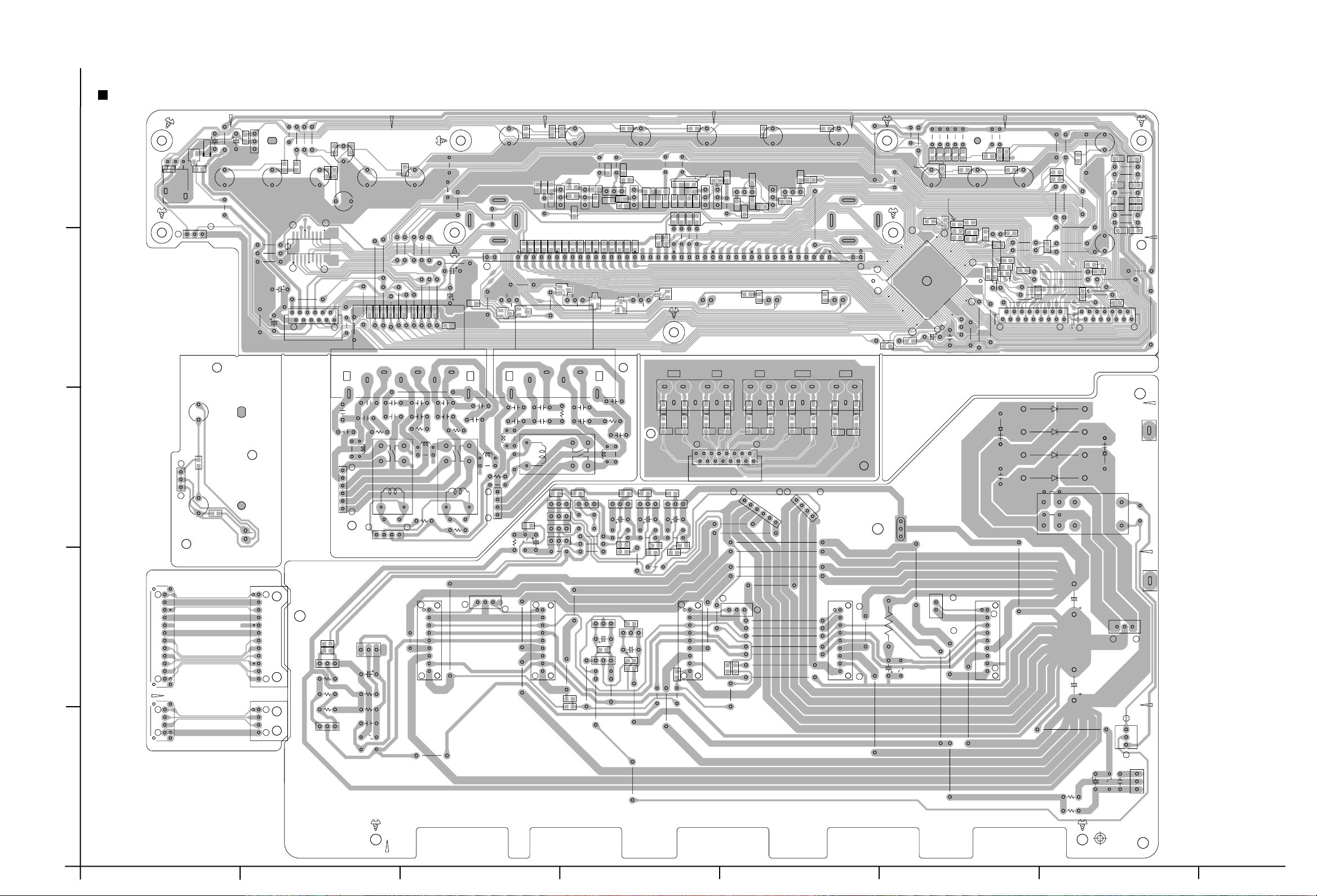
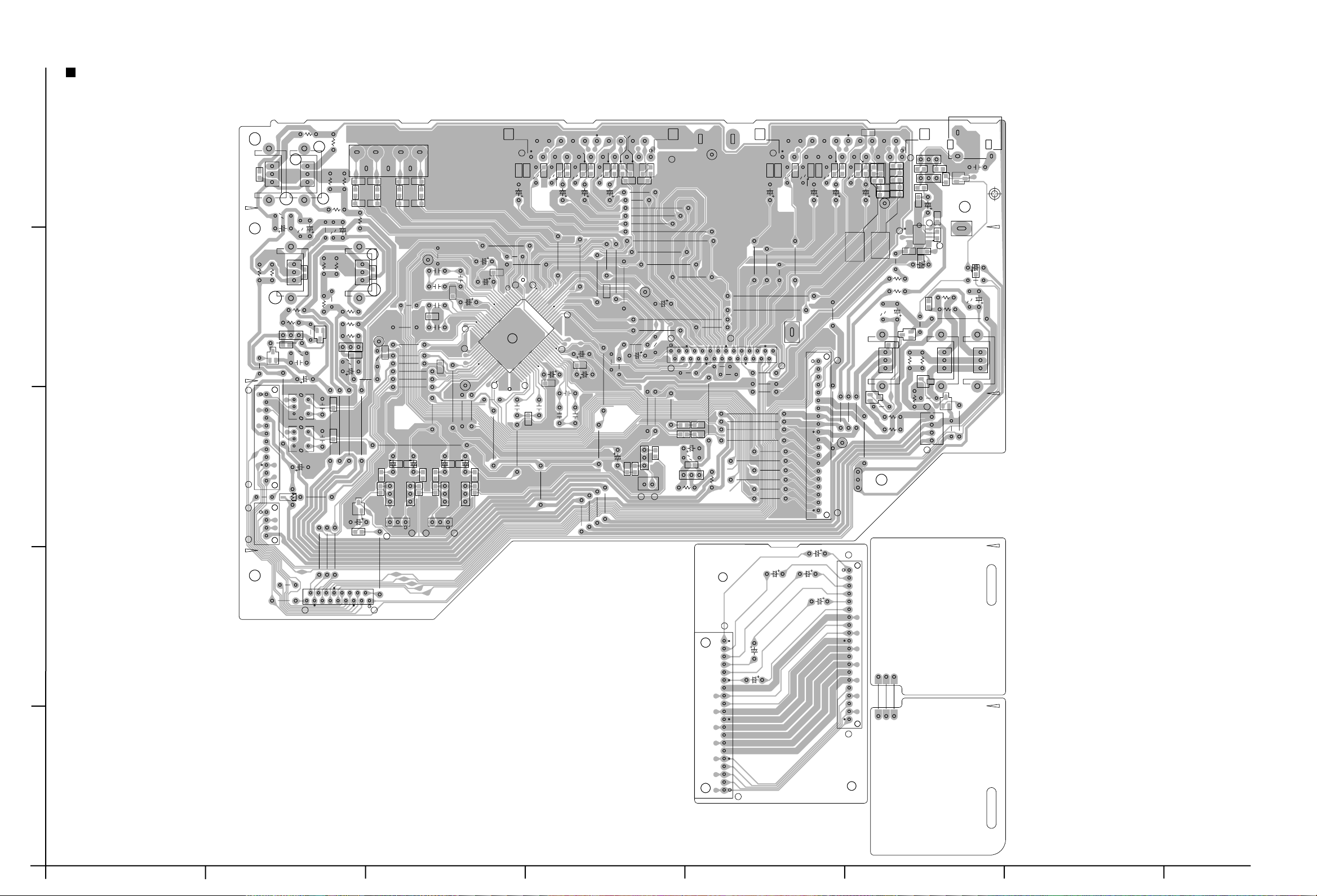
Printed circuit boards
Main & System control board
RX-E100SL
C401
C403
D408
Q407
5
R425
R426
IC403
FW401
R427
IC404
R441
S409S410
R440
IC402
C419
S413
R445
R446
S407
S414
R437
R438
S406
R449
S416
C407
R428
C408
S404
R433
C409
R1422
R1421
D404
R1420
R402
R1419
R434
R404
R406
R1418
R1417
S405
R435
R403
R408
R401
Q402
Q401
R1416
R1415
R1414
Q412
4
Q409
C406
R494
R495
R496
R497
R498
R499
ST742
C754
S422
3
R492
FW401
S421
R491
D407
C758
C759
C760
FW702
C756
C757
R749
L745
RY743
D743
FW707
R455
R489
R490
R493
R400
C752
C751
C750
C749
R748
R747
L744
RY742
D742
R743
R742
Q408
ST741
C755
C753
C748
C744
C746
C742
L742
L743
D741
R741
Q710
FW701
Q711
R726
Q713
D710
R720
C712
Q712
RY741
C743
C741
R746
R724R725
D713
D712
R442 R443
R407
Q405
R405
R1425
R424
R421
R1423
R1413
R1412
R1411
R1410
R1409
Q413
Q410
C745
R745
C747
L741
Q709
D715
R732
R731
S411 S412
R423
R419
R420
Q406
R1408
R1407
D405D406
R727R728
C714C715
D714
R730
R410 R411
R418
C411
R417
R422
R1405
R1406
Q411
C1582
C1581
R1582
R1592
R1591
Q714Q715
R729
R450
S417
R412
R409
DI401
J1582
R1581
R721
Q708
C713
D711
R723
R722
R415
R416
C410
R413
R414
Q403
Q404
R1401
R1402
R1403
R1404
C1584
R1584
R1594
CN522
R1593
Q415
R483
R1433
C1583
R1583
R1586
R1424
R484
R486
R485
R1432
C1586
Q416
R487
J1581
C1585
R1585
R1595R1596 R1598R1598
R1590
R451
S418
R461
EP701
R462
S403
R480
C404
C402
R481
R482
Q414
IC401
D401D402D403
R1431
IC401
R488
C1590
C1588
C1587
R1589
R1588
C1592
C1589
R1587
C1591
R458
R459
R460
S401
R430
R432
R478
R477
R476
C417
R479
R474
C405
X401
R453
R454
R457
R431
R473
R475
R468
R467
R471
R470
R469
R465
R472
R466
CN401
C701 C702
R448
S402
R1426
D703
D702
D704
R447
C418
D701
S408
C416
R439
C415
C414
C412
S415
R1427
R464
CN402
RY701
R456
R452
R444
R436
R429
C413
R463
R1428
C703
D716
C716
CL701 CL702
CN202
CN206
Q701
2-9
CN515
2
CN121
CN122
CN513CN514
R718
R719
Q707
R717
R716
Q706
Q705
C711
R713
R714R715
C717
D709
D708
CN714
CN713
R707
R708
Q704
C710
R712
Q703
R710
Q702
C709
R711
R709
D707
CN712
R706
CN517
R704
CN711
R705
CN516
R701
CN715
C706
D705
1
C705
C704
D706
R702
R703
C708
ABCD E F G
Page 26
Audio signal input board
RX-E100SL
C555
C561
HS514
J504
J502
Q507
R529
R531
CL502
Q517
Q516
D508
HS520
Q515
C563
C581
R1621
C562
HS515
Q508
R558
R593
IC503
R592
CN205
R532
R530
C546
C556
R554
R556
C544
R552
R591
Q520
R1626
CN503 CN504
HS526
C567
Q526
D520
R585
R596
Q518
Q519
Q521
D505
R586
C566
Q512
R595
C574
C564
FL502
FL501
5
4
3
D509
R577
C570
HS521
HS512
D519
R1625
R599
R597
R598
C559
D506
C560
R594
R587
R602
R588
Q525
Q510
C568
D503
C557
C565
C552
R576
R575
C551
C553
Q509
C554
J503
C513
C514
R525
R526
R527
C515
C516
R603
HS513
C571
Q513
R581
R582
R1624
C536
C550
R570
R572
R574
Q506
R578
CN507
C517
R1615 R1616
PW514
Q505
C518
R528
C524
R1620
C526
C528
C532
C530
R538
C534
C537
C542
C549
R569
R571
R548
R550
R573
CN505
R546
Q502
Q501
C541
R545
R549
R511
R510
D514
C506
C520
R1618
C522
C533
C531
R537
R547
R1619
R505
R508
R509
D513
R507
C529
R1617
C527
R506
D512
C504
C505
IC501
C519
C521
C523
C525
C501
R501
R503
R504
D511
R1611 R1612
C503
C535
C577
C545
R557
R559
J501
C502
R502
R1623
Q503
CN506
R534
R561
Q511
EP501
R523
R521
R522
D517
D518
R519
C512
C578
CN502
R533
R535
R536
C558
D504
C569
R583
R584
C511
CL501
CN501
C593
R516R517
R515
R518
R520
D515
D516
C509
C510
K501
R513
C591
R1613
EP502
PW504
C507
K502
C508
R514
C592
R1614
R579
R580
D507
Q523
C572
Q514
Q522
R590
R589
C606
C604C605
2
CN411
C603
C601
CN511
C602
CN601
1
2-10
HABC DEFG
Page 27
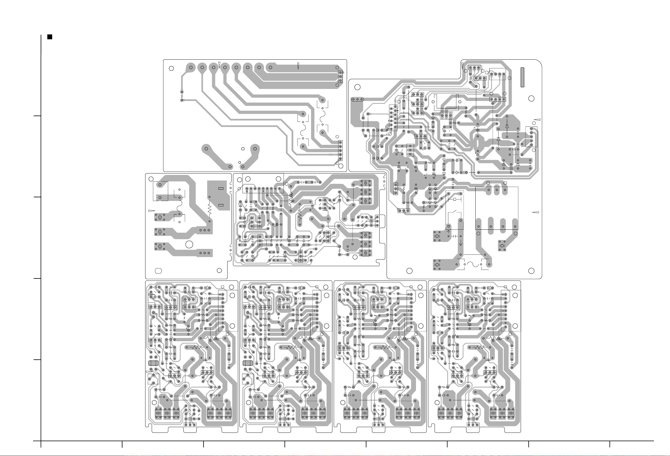
power amp. board
RX-E100SL
FW206
R935
R941
Q911
R937
D905
Q913
FW202
FW201
R939
D907
R931R933
C921C923
EP201
R929
R927
R925
D212
C213
D219
Q915Q917
TH901
Q909
CN204
Q203
C217
C212
R208
Q202
R207
D211
Q205
R203
R204
Q209
Q208
Q207
C216
C209
Q204
D216
R202
R206
D208
D220
D217
C218
D206
PW203
D207
PW201
C207
C215
D209
HS211
Q211
C221
C206
D215
D214
D210
5
C911
L901
R945
FC203
FC204
R943
R913
R949
R201
FC205
FC206
4
FC202
CN217
PW101
PW102
3
PW103
FC201
R205
TA202
TA201
EP202
CN207
CN705
C901
D901
R909
C913
C905
C907
R901
R907
C903
Q903
C915
Q905
C917
R903
R905
Q901
R963
R955
R921
R915
R957
C919
R961
R923
R959
R947
R953
C909
C929
D909
C925 C927
R951
R911
Q919
C208
C210
D221
C214
D213
R209
FC208
R212
R214
R211
RY201
C204
C205
Q212
FC207
CN707
FW205
D204
D203
PW202
D201
TH201
C202
CN201
C201
C203
D202
T202
R322
Q304
C320
R352
R344
R328
R302
R324
R332
C322
C302
R304
L302
R330
R306
C304
R336
Q312
D306
R340
Q801
R851
Q803
R863
C819
R843
R801
R829
R827
R825
TH801
Q809
R821
R823
C801
R803
L801
R805
C803
R835
Q811
D805
R839
R810
C814
C808
C806
C818
R856
R860
C830
D810
R846
R850
R842
R838
Q814
C816
Q806
D808
R816
R862
R848
C810
R812
C812
R814
R808
R858
R853
C825C827 CN703
Q820
R831R833
C821C823
Q815Q817
D802
Q804
Q802
R852
C820
R844
R864
R830
R828
R826
TH802
Q810
R822
R824
R832R834
C822C824
C802
R804
L802
R802
R806
R836
D806
R840
CN704
C804
R854
C826C828
Q812
Q816Q818
R809
R354
R807
R857
Q819
C813
C817
R855
R859
C829
D809
R845
R849
R841
R837
Q813
C807
C815
Q805
CN702
C326C328
Q316Q318
D807
R815
R861
R847
R811
C811
R813
D801
C805
C809
2-11
Q308
Q320
R334
C324
R308
D304
R318
R348
R350
C314
C318
R346
R316
D310
VR302
R310
C308
C316
Q306
R338
D302
C306
Q302
R356
R320
C310
R312
C312
R314
R342
Q314
D308
C313
R309
C317
C307
C315
Q305
R307
Q307
2
D303
R315
D309
VR301
R337
R319
C309
R311
C311
R313
R341
Q313
D307
R317
R347
Q319
R345
R349
R333
C323
D301
C305
Q301
R321
R355
R351
Q303
C319
R343
R301
R323
C301
R303
L301
R331
C321
R305
C303
R335
D305
R339
R353
C325C327 CN701
Q311
1
R327
TH301
Q309
R325
R329
Q315Q317
TH302
Q310
R326
ABCD E F G
Page 28
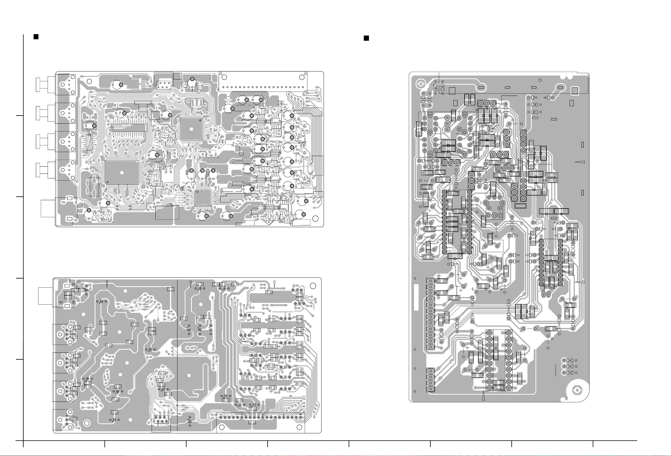
RX-E100SL
DSP board
Tuner board
Forward side
X671
K687
C610
C603
R615
C612
C605
R661
C611
TP607
C687
R687
K688
R682
R697
C673
Q672
R662
R663
R617 R618
C606
R664
C602
IC601
K681
C684
C604
IC672
R669
D607
C601
R2510
C2508
D608
R2535
C607
C681
CN681
R671
R2508
C2582
Q673
C2531
R2533
C608
TP515
TP514
TP517
R2586
R2582
C2581
Q671
R672
R2565
C2561
C2534
C2540
C2539
C2533
TP518
R2581
TP520
C682
R2518
C2518
R2507
TP519
C686
R2566
R2550
R2584
R2564
C2564
C2563
R2563
C2555
C2556
R2521
R2519
R2589
C683
C2584
R2520
C2517
R2517
C685
C661
R698
IC690
R2522
C2507
R2537
R2538
C2589
C2590
R2509
TP511
R2500
C2562
TP510
R2561
TP509
C2512
K682
IC691
IC650
R2551
R2552
C2585
C2586
C2588
TP512
C2569
C2570
IC610
CN681
R2592
C2515
R2562
C2594
IC661
IC651
C2597
C2578
C2527
R2590
R2594
R2578
R2501
R2502
C2525
C2575
C2592
IC609
C2577
C2528
R2512
C2514
R2513
R2515
R2585
C2598
R2531
R2555
R2525
R2526
R2576
R2596
R2577
R2595
R2598
R2528
C2504
C2513
R2511
C2583
R2583
R2588
R2587
R2597
R2568
R2567
R2530
C2551
R2553
C2516
C2503
TP502
C2526
R2575
C2576
C2595
IC682
Q2501
C2500
R2560
IC662
R2529
TP506
TP508
IC652
R2527
TP503
TP504
TP505
TP507
C2587
R2558
R2557
R2536
R2516
R2514
TP501
R2534
C2532
R2556
R2532
R2554
C2552
B123
C157
C168
C133
C136
C162
B171
T111
C117
R158
L111
L112
C158
C161
R157
CN111
D126
B199
R140
C113
B183
C135
E
B180
30
IC102
16
R162
R183
CN112
B173
R161
D127
C111
[DOM]
Q111
C118
R146
D123
C137
C139
C185
R141
R182
D121
R147
C138
C140
C186
B
B104
C141
C134
B133
C199
[DOM]
B176
B177
B188
X191
C112
[DOM]
CF102
D131
R109
C149
R115
[DOM]
151
B132
R191
E
R108
C144
R142
C163
R193
C191
R111
C165
C150
R145
Q112
B124
C164
C192
B197
R150
B196
C143
C148
B198
C146
R144
C194
R192
B
Q103
C105
C184
R194
Q113
R114
C197
IC191
E
R107
R143
B131
B178
R112
CF101
T142
CF103
C147
B175
C107
Q121
B
BE
R105
R126
Q102
R106
B103
AT101
B174
R104
EB
R103
B182
B122
B121
C195
B187
C193
B192
B181
R130
C196
C101
B195
R184
B105
B191
C122
B194
R134
D124
D125
B190
B189
B134
X121
C130
T2D
B135
B151
R128
C103
B172
R119
R129
IC121
C121
1
B193
B186
B102
C123
C128
C126
C129
RF101
R133
R132
D129
R122
R124
R127
B106
B113
B112
B111
R670
R694
R632
R643
CN687
C672
Q601
R601
R602
R609
R684
LC632
R685
IC683
R606
R607
R608
R673
R612
R611
Q670
R613
R693
R677
C677
R692
R603
C688
IC671
R691
5
4
J601
UN663 UN664
UN662
UN661
K602
C648
R647
C647
K601
C621
LC631
C631
IC622
R627
R621
C638
IC611
C628
X631
R628
R639
C690
LC641
IC621
IC631
IC681
C654
R642
R648
R681
LC671
R688 R689
R679R680
R674
C679
R678
R695
R696
IC641
R657
Q607
C641
R686
C643
C644
R633
C645
R641
R645
R644
R646
C649
3
Reverse side
K603
C623
R622
C622
2
TP603
TP604
TP602
1
TP605
R630
C624
C629
R623
R625
C625
R629
C637
R624
R626
TP601
C626
C636
C639
R631
C646
C635
C634
R640
C689
C653
C633
C632
TP606
C671
C693
C642
CN687
C694
C609
R675
R676
R683
2-12
HABC DEFG
Page 29

PARTS LIST
[ RX-E100SL ]
* All printed circuit boards and its assemblies are not available as service parts.
Area suffix
RX-E100SL
- Contents -
Exploded view of general assembly and parts list
Electrical parts list
Packing materials and accessories parts list
J ----------------------------- U.S.A.
C -------------------------- Canada
3- 3
3- 5
3-16
3-1
Page 30

RX-E100SL
< MEMO >
3-2
Page 31

RX-E100SL
Exploded view of general assembly and parts list
Block No.
64
M
5
59
58
M
1
M
60
39
41
72
43
55
56
44
52
53
51
48
42
43
49
45
43
61
4
57
65
3
12
5
6
19
2
1
66
7
17
38
38
21
16
59
32
30
40
34
28
31
28
28
28
27
32
31
29
34
35
54
3328
46
69
68
37
36
23
67
70
54
35
24
24
23
2
66
13
14
11
22
1
4
18
3
8
ABCD E F G
20
25
26
3-3
Page 32
RX-E100SL
)
)
A
Parts list
Item Parts number Parts name Area
A
1 LV10482-002A FRONT PANEL 1
2 VJD5429-002SS JVC MARK 1
3 E75896-003 FELT SPACER 2 FOR FRONT FOOT
4 LV20958-001A LENS 1
5 LV20991-002A POWER BUTTON 1
6 LV42096-001A INDICATOR 1
7 LV32517-001A CONTROL BUTTON 1
8 LV20959-002A SOURCE BUTTON 1
11 LV20992-001A VOLUME BUTTON 1
12 QYSBSF2608Z T.SCREW 2 F.C.B.POWER+F.PANEL
13 LV42195-001A FL SCREEN 1 TO FRONT PANEL
14 QYSBSF2608Z T.SCREW 7 F.C.B.FL+F.PANE
16 QUQ412-1738CJ FFC WIRE 1
17 QUQ412-1213CJ FFC WIRE 1
18 QYSBSG3006Z T.SCREW 4 F.PANEL+C.BASE
19 QYSBSG3006Z T.SCREW 3 F.PANEL+F.BKT
20 LV10019-003A CHASSIS BASE 1
21 LV10483-001A FRONT BRACKET 1
22 QYSBSG3006Z T.SCREW 5 C.BASE+F.BKT
23 E68587-223SM CB BKT 3
24 QYSBSG3006Z T.SCREW 3 CB BKT+C.BASE
25 E47227-021 FOOT ASS'Y 2
26 QYSBSG3006Z T.SCREW 2 FOOT ASS'Y+C.BASE
27 LV20960-001A HEAT SINK 1
28 E73525-003SS SCREW 10 TR
29 LV32433-001A H.S BRACKET(R
30 LV32434-001A H.S BRACKET(L
31 QYSBSG3008Z T.SCREW 4 H.SINK BKT+H.SINK
32 QYSBSG3006Z T.SCREW 2 H.SINK BKT+F.BKT
33 QYSBSG3006Z T.SCREW 2 AMP M.C.B+H.SINK BKT
34 QYSBSG3006Z T.SCREW 2 H.SINK BKT+C.BASE
35 QYSBSG3006Z T.SCREW 3 A.M.C.B+C.B.&CB BKT
36 LV42098-001A C.B BKT 1
37 QYSBSG3006Z T.SCREW 1 C.B.BKT+C.BASE
38 QYSBSG3006Z T.SCREW 3 T.C.B+C.BASE&F.BKT
39 QYSBSG3006Z T.SCREW 1 P.CORD C.B+C.BASE
40 QQT0327-001 POWER TRANSF
41 QYSDSTL4008Z SPECIAL SCREW 4 P.TRANS
42 LV20961-008A REAR PANEL C1
43 QYSBSGY3008M SPECIAL SCREW 3 R.PANEL+C.BASE
44 QYSBSGY3008M SPECIAL SCREW 1 R.PANEL+ud--45 QYSBSGY3008M SPECIAL SCREW 2 TUNER
46 QUQ412-1607CJ FFC WIRE 1
48 QYSBSGY3008M SPECIAL SCREW 1 SUB WOOFER
49 QYSBSGY3008M SPECIAL SCREW 2 PIN JACK
51 QYSBSGY3008M SPECIAL SCREW 2 DIGITAL
52 QYSBSGY3008M SPECIAL SCREW 2 F.SPK TERM.+R.PANEL
(General assembly)
Q'ty Description
LV20961-007A REAR PANEL J1
Block No. M1MM
1
1
1 T201
Parts list
Item Parts number Parts name Area
A
53 QYSBSGY3008M SPECIAL SCREW 2 R.SPK TERM.+R.PANEL
54 QYSBSG3006Z T.SCREW 3 INPUT M.C.B+C.BASE
55 QMPD220-200-JD POWER CORD
A
56 QZW0033-001 STRAIN RELIEF
A
57 LV20962-001A/S/ TOP COVER 1
58 QYSBSGY3008M SPECIAL SCREW 3
59 E406308-004 SPECIAL SCREW 4
60 QMF51U1-5R0-J8 FUSE
A
61 QMF51U1-2R0-J8 FUSE
A
64 E409394-001 CAUTION LABEL J1
65 QYSBSG3008E T.SCREW 1
66 LV30225-0C1A FELT SPACER 2 FS400 FS401
67 QYSBSG3008E T.SCREW 1
68 QYSBSG3008E T.SCREW 1
69 QYSBSG3008E T.SCREW 2
70 QYSBSG3008E T.SCREW 1
72 LV42388-001A FUSE CAUTION 1 STICK ON REAR INSIDE
(General assembly)
Q'ty Description
1
1
1 F201
2 F202 F203
E409396-002 CAUTION LABEL C1
Block No. M1MM
3-4
Page 33

RX-E100SL
Electrical parts list
Item
A
C 201 QFLC2AJ-104Z M CAPACITOR .10MF 5% 100V
C 202 QFLC2AJ-104Z M CAPACITOR .10MF 5% 100V
C 203 QFLC2AJ-104Z M CAPACITOR .10MF 5% 100V
C 204 QETM1VM-228 E CAPACITOR 2200MF 20% 35V
C 205 QETM1VM-108 E CAPACITOR 1000MF 20% 35V
C 206 QFLC1HJ-473Z M CAPACITOR .047MF 5% 50V
C 207 QFLC1HJ-473Z M CAPACITOR .047MF 5% 50V
C 208 QFLC2AJ-472Z M CAPACITOR 4700PF 5% 100V
C 209 QETN1EM-477Z E CAPACITOR 470MF 20% 25V
C 210 QCZ9104-472 C CAPACITOR
A
C 212 QETN1CM-477Z E CAPACITOR 470MF 20% 16V
C 213 QETN0JM-228Z E CAPACITOR 2200MF 20% 6.3V
C 214 QETN1HM-227Z E CAPACITOR 220MF 20% 50V
C 215 QETN1JM-107Z E CAPACITOR 100MF 20% 63V
C 216 QETN1HM-226Z E CAPACITOR 22MF 20% 50V
C 217 QETN1HM-226Z E CAPACITOR 22MF 20% 50V
C 218 QETN1HM-105Z E CAPACITOR 1.0MF 20% 50V
C 221 QETN1EM-107Z E CAPACITOR 100MF 20% 25V
C 301 QETN1HM-225Z E CAPACITOR 2.2MF 20% 50V
C 302 QETN1HM-225Z E CAPACITOR 2.2MF 20% 50V
C 303 QCS31HJ-271Z C CAPACITOR 270PF 5% 50V
C 304 QCS31HJ-271Z C CAPACITOR 270PF 5% 50V
C 305 QCS31HJ-101Z C CAPACITOR 100PF 5% 50V
C 306 QCS31HJ-101Z C CAPACITOR 100PF 5% 50V
C 307 QCB31HK-152Z C CAPACITOR 1500PF 10% 50V
C 308 QCB31HK-152Z C CAPACITOR 1500PF 10% 50V
C 309 QETN1CM-107Z E CAPACITOR 100MF 20% 16V
C 310 QETN1CM-107Z E CAPACITOR 100MF 20% 16V
C 311 QCS31HJ-220Z C CAPACITOR 22PF 5% 50V
C 312 QCS31HJ-220Z C CAPACITOR 22PF 5% 50V
C 313 QFLC1HJ-103Z M CAPACITOR .010MF 5% 50V
C 314 QFLC1HJ-103Z M CAPACITOR .010MF 5% 50V
C 315 QCS32HJ-220Z C CAPACITOR 22PF 5% 500V
C 316 QCS32HJ-220Z C CAPACITOR 22PF 5% 500V
C 317 QETN1CM-107Z E CAPACITOR 100MF 20% 16V
C 318 QETN1CM-107Z E CAPACITOR 100MF 20% 16V
C 319 QETN1JM-107Z E CAPACITOR 100MF 20% 63V
C 320 QETN1JM-107Z E CAPACITOR 100MF 20% 63V
C 321 QCS32HJ-470Z C CAPACITOR 47PF 5% 500V
C 322 QCS32HJ-470Z C CAPACITOR 47PF 5% 500V
C 323 QCS32HJ-470Z C CAPACITOR 47PF 5% 500V
C 324 QCS32HJ-470Z C CAPACITOR 47PF 5% 500V
C 325 QFLC1HJ-473Z M CAPACITOR .047MF 5% 50V
C 326 QFLC1HJ-473Z M CAPACITOR .047MF 5% 50V
C 327 QFLC1HJ-473Z M CAPACITOR .047MF 5% 50V
C 328 QFLC1HJ-473Z M CAPACITOR .047MF 5% 50V
C 801 QETN1HM-225Z E CAPACITOR 2.2MF 20% 50V
C 802 QETN1HM-225Z E CAPACITOR 2.2MF 20% 50V
C 803 QCS31HJ-271Z C CAPACITOR 270PF 5% 50V
C 804 QCS31HJ-271Z C CAPACITOR 270PF 5% 50V
C 805 QCS31HJ-101Z C CAPACITOR 100PF 5% 50V
C 806 QCS31HJ-101Z C CAPACITOR 100PF 5% 50V
C 807 QCB31HK-152Z C CAPACITOR 1500PF 10% 50V
C 808 QCB31HK-152Z C CAPACITOR 1500PF 10% 50V
C 809 QETN1CM-476Z E CAPACITOR 47MF 20% 16V
C 810 QETN1CM-476Z E CAPACITOR 47MF 20% 16V
C 811 QCS31HJ-220Z C CAPACITOR 22PF 5% 50V
C 812 QCS31HJ-220Z C CAPACITOR 22PF 5% 50V
C 813 QFLC1HJ-103Z M CAPACITOR .010MF 5% 50V
C 814 QFLC1HJ-103Z M CAPACITOR .010MF 5% 50V
C 815 QCS32HJ-330Z C CAPACITOR 33PF 5% 500V
C 816 QCS32HJ-330Z C CAPACITOR 33PF 5% 500V
C 817 QETN1CM-107Z E CAPACITOR 100MF 20% 16V
Parts number Parts name Area
(Power amp board)
Remarks
4700PF
Block No. 01
Item
A
C 818 QETN1CM-107Z E CAPACITOR 100MF 20% 16V
C 819 QETN2AM-106Z E CAPACITOR 10MF 20% 100V
C 820 QETN2AM-106Z E CAPACITOR 10MF 20% 100V
C 821 QCS32HJ-470Z C CAPACITOR 47PF 5% 500V
C 822 QCS32HJ-470Z C CAPACITOR 47PF 5% 500V
C 823 QCS32HJ-470Z C CAPACITOR 47PF 5% 500V
C 824 QCS32HJ-470Z C CAPACITOR 47PF 5% 500V
C 825 QFLC1HJ-473Z M CAPACITOR .047MF 5% 50V
C 826 QFLC1HJ-473Z M CAPACITOR .047MF 5% 50V
C 827 QFLC1HJ-473Z M CAPACITOR .047MF 5% 50V
C 828 QFLC1HJ-473Z M CAPACITOR .047MF 5% 50V
C 829 QETN1HM-476Z E CAPACITOR 47MF 20% 50V
C 830 QETN1HM-476Z E CAPACITOR 47MF 20% 50V
C 901 QETN1HM-225Z E CAPACITOR 2.2MF 20% 50V
C 903 QCS31HJ-271Z C CAPACITOR 270PF 5% 50V
C 905 QCS31HJ-101Z C CAPACITOR 100PF 5% 50V
C 907 QCB31HK-152Z C CAPACITOR 1500PF 10% 50V
C 909 QETN1CM-476Z E CAPACITOR 47MF 20% 16V
C 911 QCS31HJ-220Z C CAPACITOR 22PF 5% 50V
C 913 QFLC1HJ-103Z M CAPACITOR .010MF 5% 50V
C 915 QCS32HJ-330Z C CAPACITOR 33PF 5% 500V
C 917 QETN1CM-107Z E CAPACITOR 100MF 20% 16V
C 919 QETN2AM-106Z E CAPACITOR 10MF 20% 100V
C 921 QCS32HJ-470Z C CAPACITOR 47PF 5% 500V
C 923 QCS32HJ-470Z C CAPACITOR 47PF 5% 500V
C 925 QFLC1HJ-473Z M CAPACITOR .047MF 5% 50V
C 927 QFLC1HJ-473Z M CAPACITOR .047MF 5% 50V
C 929 QETN1HM-476Z E CAPACITOR 47MF 20% 50V
CN201 QGD2501C1-05Z SOCKET
CN204 QGF1205C1-12 CONNECTOR
CN207 WJK0037-001A E-SI C WIRE C-B
CN217 QGA7901C1-02 CONNECTOR
CN701 QGB2510K1-09 CONNECTOR
CN702 QGB2510K1-09 CONNECTOR
CN703 QGB2510K1-09 CONNECTOR
CN704 QGB2510K1-09 CONNECTOR
CN705 QGB2510K1-09 CONNECTOR
CN707 QGD2501C1-04Z SOCKET
D 201 10E2-FD DIODE
A
D 202 1SR35-400A-T5 DIODE
A
D 203 10E2-FD DIODE
A
D 204 1SR35-400A-T5 DIODE
A
D 206 1SR35-400A-T5 DIODE
A
D 207 1SR35-400A-T5 DIODE
A
D 208 1SR35-400A-T5 DIODE
A
D 209 1SR35-400A-T5 DIODE
A
D 210 1SS133-T2 SI DIODE
D 211 MTZJ6.2C-T2 Z DIODE
D 212 1SR35-400A-T5 DIODE
D 213 1SR35-400A-T5 DIODE
A
D 214 1SR35-400A-T5 DIODE
A
D 215 1SR35-400A-T5 DIODE
A
D 216 MTZJ27C-T2 Z DIODE
D 217 MTZJ6.2C-T2 Z DIODE
D 219 1SR35-400A-T5 DIODE
D 220 1SR35-400A-T5 DIODE
D 221 MTZJ6.2C-T2 Z DIODE
D 301 1SS133-T2 SI DIODE
D 302 1SS133-T2 SI DIODE
D 303 SLR-342MC-T LED
D 304 SLR-342MC-T LED
D 305 1SS133-T2 SI DIODE
D 306 1SS133-T2 SI DIODE
Parts number Parts name Area
Remarks
3-5
Page 34

RX-E100SL
(
)
(
)
(
)
(
)
(
)
(
)
Q
Q
Q
Q
Q
Q
Q
Q
Q
Q
Q
Q
Q
Q
Q
Q
Q
Q
Q
Q
Q
Q
Q
Q
Q
Q
Q
Q
Q
Q
Q
Q
Q
Q
Q
Q
Q
Q
Q
Q
Q
Q
Q
Q
Q
Q
Q
Q
Q
Q
Q
Q
Q
Q
Q
Electrical parts list
Item
A
D 307 1SS133-T2 SI DIODE
D 308 1SS133-T2 SI DIODE
D 309 1SS133-T2 SI DIODE
D 310 1SS133-T2 SI DIODE
D 801 1SS133-T2 SI DIODE
D 802 1SS133-T2 SI DIODE
D 805 1SS133-T2 SI DIODE
D 806 1SS133-T2 SI DIODE
D 807 1SS133-T2 SI DIODE
D 808 1SS133-T2 SI DIODE
D 809 1SS133-T2 SI DIODE
D 810 1SS133-T2 SI DIODE
D 901 1SS133-T2 SI DIODE
D 905 1SS133-T2 SI DIODE
D 907 1SS133-T2 SI DIODE
D 909 1SS133-T2 SI DIODE
EP201 QNZ0136-001Z EARTH PLATE
EP202 E409182-001SM GRAND TERMINAL
FC201 QNG0020-001Z FUSE CLIP
FC202 QNG0020-001Z FUSE CLIP
FC203 QNG0020-001Z FUSE CLIP
FC204 QNG0020-001Z FUSE CLIP
FC205 QNG0020-001Z FUSE CLIP
FC206 QNG0020-001Z FUSE CLIP
FW201 QUM135-22DGZ4 PARA RIBON WIRE
FW202 QJK017-031301 SIN CR C-B WIR
FW205 QUM134-22DGZ4 PARA RIBON WIRE
FW206 QUM133-08DGZ4 PARA RIBON WIRE
HS211 E70306-001 HEAT SINK
L 301 QQLZ005-R45 INDUCTOR
L 302 QQLZ005-R45 INDUCTOR
L 801 QQLZ005-R45 INDUCTOR
L 802 QQLZ005-R45 INDUCTOR
L 901 QQLZ005-R45 INDUCTOR
A
A
A
A
A
A
Parts number Parts name Area
202 KRC105M-T D TRANSISTOR
203 KTC3203/OY/-T TRANSISTOR
204 KTA1046/Y/ TRANSISTOR
205 KTC3200/GL/-T TRANSISTOR
207 KRC105M-T D TRANSISTOR
208 KRC105M-T D TRANSISTOR
209 KRC105M-T D TRANSISTOR
211 2SD2395/EF/ TRANSISTOR
301 2SC2240/L/-T TRANSISTOR
302 2SC2240/L/-T TRANSISTOR
303 2SC2240/L/-T TRANSISTOR
304 2SC2240/L/-T TRANSISTOR
305 KTA1268/GL/-T TRANSISTOR
306 KTA1268/GL/-T TRANSISTOR
307 KTC3200/GL/-T TRANSISTOR
308 KTC3200/GL/-T TRANSISTOR
309 2SD637/QR/ TRANSISTOR
310 2SD637/QR/ TRANSISTOR
311 KTC3200/GL/-T TRANSISTOR
312 KTC3200/GL/-T TRANSISTOR
313 KTA1268/GL/-T TRANSISTOR
314 KTA1268/GL/-T TRANSISTOR
315 2SD2389/OPY/-F6 TRANSISTOR
316 2SD2389/OPY/-F6 TRANSISTOR
317 2SB1559/OPY/-F6 TRANSISTOR
318 2SB1559/OPY/-F6 TRANSISTOR
319 KTA1268/GL/-T TRANSISTOR
320 KTA1268/GL/-T TRANSISTOR
801 2SC2240/L/-T TRANSISTOR
(Power amp board)
F201
F201
F202
F202
F203
F203
Remarks
Block No. 01
Item
A
A
A
A
A
A
A
R 201 QRJ146J-5R6X UNF C RESISTORA5.6 5% 1/4W
R 202 QRJ146J-100X UNF C RESISTORA10 5% 1/4W
R 203 QRJ146J-100X UNF C RESISTORA10 5% 1/4W
R 204 QRJ146J-821X UNF C RESISTORA820 5% 1/4W
R 205 QRZ9044-335 COMP RESISTORA3.3M 1/0W
R 206 QRJ146J-332X UNF C RESISTORA3.3K 5% 1/4W
R 207 QRE141J-223Y C RESISTOR 22K 5% 1/4W
R 208 QRJ146J-100X UNF C RESISTORA10 5% 1/4W
R 209 QRE141J-104Y C RESISTOR 100K 5% 1/4W
R 211 QRZ9005-120X F RESISTOR
A
R 212 QRJ146J-682X UNF C RESISTORA6.8K 5% 1/4W
R 213 QRE141J-331Y C RESISTOR 330 5% 1/4W
R 301 QRE141J-222Y C RESISTOR 2.2K 5% 1/4W
R 302 QRE141J-222Y C RESISTOR 2.2K 5% 1/4W
R 303 QRE141J-563Y C RESISTOR 56K 5% 1/4W
R 304 QRE141J-563Y C RESISTOR 56K 5% 1/4W
R 305 QRE141J-123Y C RESISTOR 12K 5% 1/4W
R 306 QRE141J-123Y C RESISTOR 12K 5% 1/4W
R 307 QRE141J-332Y C RESISTOR 3.3K 5% 1/4W
R 308 QRE141J-332Y C RESISTOR 3.3K 5% 1/4W
R 309 QRE141J-101Y C RESISTOR 100 5% 1/4W
R 310 QRE141J-101Y C RESISTOR 100 5% 1/4W
R 311 QRJ146J-391X UNF C RESISTORA390 5% 1/4W
R 312 QRJ146J-391X UNF C RESISTORA390 5% 1/4W
R 313 QRE141J-563Y C RESISTOR 56K 5% 1/4W
R 314 QRE141J-563Y C RESISTOR 56K 5% 1/4W
R 315 QRJ146J-331X UNF C RESISTORA330 5% 1/4W
R 316 QRJ146J-331X UNF C RESISTORA330 5% 1/4W
R 317 QRE141J-473Y C RESISTOR 47K 5% 1/4W
R 318 QRE141J-473Y C RESISTOR 47K 5% 1/4W
R 319 QRJ146J-331X UNF C RESISTORA330 5% 1/4W
R 320 QRJ146J-331X UNF C RESISTORA330 5% 1/4W
R 321 QRJ146J-100X UNF C RESISTORA10 5% 1/4W
R 322 QRJ146J-100X UNF C RESISTORA10 5% 1/4W
R 323 QRJ146J-100X UNF C RESISTORA10 5% 1/4W
R 324 QRJ146J-100X UNF C RESISTORA10 5% 1/4W
R 325 QRE141J-361Y C RESISTOR 360 5% 1/4W
Parts number Parts name Area
802 2SC2240/L/-T TRANSISTOR
803 2SC2240/L/-T TRANSISTOR
804 2SC2240/L/-T TRANSISTOR
805 KTA1268/GL/-T TRANSISTOR
806 KTA1268/GL/-T TRANSISTOR
809 2SD637/QR/ TRANSISTOR
810 2SD637/QR/ TRANSISTOR
811 KTC3200/GL/-T TRANSISTOR
812 KTC3200/GL/-T TRANSISTOR
813 KTA1268/GL/-T TRANSISTOR
814 KTA1268/GL/-T TRANSISTOR
815 2SD2389/OPY/-F6 TRANSISTOR
816 2SD2389/OPY/-F6 TRANSISTOR
817 2SB1559/OPY/-F6 TRANSISTOR
818 2SB1559/OPY/-F6 TRANSISTOR
819 KTA1268/GL/-T TRANSISTOR
820 KTA1268/GL/-T TRANSISTOR
901 2SC2240/L/-T TRANSISTOR
903 2SC2240/L/-T TRANSISTOR
905 KTA1268/GL/-T TRANSISTOR
909 2SD637/QR/ TRANSISTOR
911 KTC3200/GL/-T TRANSISTOR
913 KTA1268/GL/-T TRANSISTOR
915 2SD2389/OPY/-F6 TRANSISTOR
917 2SB1559/OPY/-F6 TRANSISTOR
919 KTA1268/GL/-T TRANSISTOR
12 1/0W
Remarks
3-6
Page 35

RX-E100SL
Electrical parts list
Item
A
R 326 QRE141J-361Y C RESISTOR 360 5% 1/4W
R 327 QRE141J-471Y C RESISTOR 470 5% 1/4W
R 328 QRE141J-471Y C RESISTOR 470 5% 1/4W
R 329 QRE141J-471Y C RESISTOR 470 5% 1/4W
R 330 QRE141J-471Y C RESISTOR 470 5% 1/4W
R 331 QRJ146J-100X UNF C RESISTORA10 5% 1/4W
R 332 QRJ146J-100X UNF C RESISTORA10 5% 1/4W
R 333 QRJ146J-100X UNF C RESISTORA10 5% 1/4W
R 334 QRJ146J-100X UNF C RESISTORA10 5% 1/4W
R 335 QRE141J-121Y C RESISTOR 120 5% 1/4W
R 336 QRE141J-121Y C RESISTOR 120 5% 1/4W
R 337 QRE141J-121Y C RESISTOR 120 5% 1/4W
R 338 QRE141J-121Y C RESISTOR 120 5% 1/4W
R 339 QRE141J-181Y C RESISTOR 180 5% 1/4W
R 340 QRE141J-181Y C RESISTOR 180 5% 1/4W
R 341 QRE141J-181Y C RESISTOR 180 5% 1/4W
R 342 QRE141J-181Y C RESISTOR 180 5% 1/4W
R 343 QRZ0218-R22 EMIT RESISTOR 1/2W
R 344 QRZ0218-R22 EMIT RESISTOR 1/2W
R 345 QRE141J-102Y C RESISTOR 1.0K 5% 1/4W
R 346 QRE141J-102Y C RESISTOR 1.0K 5% 1/4W
R 347 QRE141J-153Y C RESISTOR 15K 5% 1/4W
R 348 QRE141J-153Y C RESISTOR 15K 5% 1/4W
R 349 QRE141J-473Y C RESISTOR 47K 5% 1/4W
R 350 QRE141J-473Y C RESISTOR 47K 5% 1/4W
R 351 QRJ125J-330 UNF C RESISTORA33 5% 1/2W
R 352 QRJ125J-330 UNF C RESISTORA33 5% 1/2W
R 353 QRL022J-100 UNF OMF RESISTORA10 5% 1/2W
R 354 QRL022J-100 UNF OMF RESISTORA10 5% 1/2W
R 801 QRE141J-222Y C RESISTOR 2.2K 5% 1/4W
R 802 QRE141J-222Y C RESISTOR 2.2K 5% 1/4W
R 803 QRE141J-563Y C RESISTOR 56K 5% 1/4W
R 804 QRE141J-563Y C RESISTOR 56K 5% 1/4W
R 805 QRE141J-183Y C RESISTOR 18K 5% 1/4W
R 806 QRE141J-183Y C RESISTOR 18K 5% 1/4W
R 807 QRE141J-302Y C RESISTOR 3.0K 5% 1/4W
R 808 QRE141J-302Y C RESISTOR 3.0K 5% 1/4W
R 809 QRE141J-101Y C RESISTOR 100 5% 1/4W
R 810 QRE141J-101Y C RESISTOR 100 5% 1/4W
R 811 QRJ146J-391X UNF C RESISTORA390 5% 1/4W
R 812 QRJ146J-391X UNF C RESISTORA390 5% 1/4W
R 813 QRE141J-563Y C RESISTOR 56K 5% 1/4W
R 814 QRE141J-563Y C RESISTOR 56K 5% 1/4W
R 815 QRJ146J-221X UNF C RESISTORA220 5% 1/4W
R 816 QRJ146J-221X UNF C RESISTORA220 5% 1/4W
R 821 QRJ146J-100X UNF C RESISTORA10 5% 1/4W
R 822 QRJ146J-100X UNF C RESISTORA10 5% 1/4W
R 823 QRJ146J-100X UNF C RESISTORA10 5% 1/4W
R 824 QRJ146J-100X UNF C RESISTORA10 5% 1/4W
R 825 QRE141J-361Y C RESISTOR 360 5% 1/4W
R 826 QRE141J-361Y C RESISTOR 360 5% 1/4W
R 827 QRE141J-751Y C RESISTOR 750 5% 1/4W
R 828 QRE141J-751Y C RESISTOR 750 5% 1/4W
R 829 QRE141J-471Y C RESISTOR 470 5% 1/4W
R 830 QRE141J-471Y C RESISTOR 470 5% 1/4W
R 831 QRJ146J-100X UNF C RESISTORA10 5% 1/4W
R 832 QRJ146J-100X UNF C RESISTORA10 5% 1/4W
R 833 QRJ146J-100X UNF C RESISTORA10 5% 1/4W
R 834 QRJ146J-100X UNF C RESISTORA10 5% 1/4W
R 835 QRE141J-181Y C RESISTOR 180 5% 1/4W
R 836 QRE141J-181Y C RESISTOR 180 5% 1/4W
R 837 QRE141J-181Y C RESISTOR 180 5% 1/4W
R 838 QRE141J-181Y C RESISTOR 180 5% 1/4W
Parts number Parts name Area
(Power amp board)
Remarks
Block No. 01
Item
A
R 839 QRE141J-181Y C RESISTOR 180 5% 1/4W
R 840 QRE141J-181Y C RESISTOR 180 5% 1/4W
R 841 QRE141J-181Y C RESISTOR 180 5% 1/4W
R 842 QRE141J-181Y C RESISTOR 180 5% 1/4W
R 843 QRZ0218-R22 EMIT RESISTOR 1/2W
R 844 QRZ0218-R22 EMIT RESISTOR 1/2W
R 845 QRE141J-102Y C RESISTOR 1.0K 5% 1/4W
R 846 QRE141J-102Y C RESISTOR 1.0K 5% 1/4W
R 847 QRE141J-183Y C RESISTOR 18K 5% 1/4W
R 848 QRE141J-183Y C RESISTOR 18K 5% 1/4W
R 849 QRE141J-123Y C RESISTOR 12K 5% 1/4W
R 850 QRE141J-123Y C RESISTOR 12K 5% 1/4W
R 851 QRJ125J-330 UNF C RESISTORA33 5% 1/2W
R 852 QRJ125J-330 UNF C RESISTORA33 5% 1/2W
R 853 QRL022J-100 UNF OMF RESISTORA10 5% 1/2W
R 854 QRL022J-100 UNF OMF RESISTORA10 5% 1/2W
R 855 QRE141J-332Y C RESISTOR 3.3K 5% 1/4W
R 856 QRE141J-332Y C RESISTOR 3.3K 5% 1/4W
R 857 QRE141J-332Y C RESISTOR 3.3K 5% 1/4W
R 858 QRE141J-332Y C RESISTOR 3.3K 5% 1/4W
R 859 QRE141J-332Y C RESISTOR 3.3K 5% 1/4W
R 860 QRE141J-332Y C RESISTOR 3.3K 5% 1/4W
R 861 QRE141J-332Y C RESISTOR 3.3K 5% 1/4W
R 862 QRE141J-332Y C RESISTOR 3.3K 5% 1/4W
R 901 QRE141J-222Y C RESISTOR 2.2K 5% 1/4W
R 903 QRE141J-563Y C RESISTOR 56K 5% 1/4W
R 905 QRE141J-183Y C RESISTOR 18K 5% 1/4W
R 907 QRE141J-302Y C RESISTOR 3.0K 5% 1/4W
R 909 QRE141J-101Y C RESISTOR 100 5% 1/4W
R 911 QRJ146J-391X UNF C RESISTORA390 5% 1/4W
R 913 QRE141J-563Y C RESISTOR
A
R 915 QRJ146J-221X UNF C RESISTORA220 5% 1/4W
R 921 QRJ146J-100X UNF C RESISTORA10 5% 1/4W
R 923 QRJ146J-100X UNF C RESISTORA10 5% 1/4W
R 925 QRE141J-361Y C RESISTOR 360 5% 1/4W
R 927 QRE141J-751Y C RESISTOR 750 5% 1/4W
R 929 QRE141J-471Y C RESISTOR 470 5% 1/4W
R 931 QRJ146J-100X UNF C RESISTORA10 5% 1/4W
R 933 QRJ146J-100X UNF C RESISTORA10 5% 1/4W
R 935 QRE141J-181Y C RESISTOR 180 5% 1/4W
R 937 QRE141J-181Y C RESISTOR 180 5% 1/4W
R 939 QRE141J-181Y C RESISTOR 180 5% 1/4W
R 941 QRE141J-181Y C RESISTOR 180 5% 1/4W
R 943 QRZ0218-R22 EMIT RESISTOR 1/2W
R 945 QRE141J-102Y C RESISTOR 1.0K 5% 1/4W
R 947 QRE141J-183Y C RESISTOR 18K 5% 1/4W
R 949 QRE141J-473Y C RESISTOR 47K 5% 1/4W
R 951 QRJ125J-330 UNF C RESISTORA33 5% 1/2W
R 953 QRL022J-100 UNF OMF RESISTORA10 5% 1/2W
R 955 QRE141J-332Y C RESISTOR 3.3K 5% 1/4W
R 957 QRE141J-332Y C RESISTOR 3.3K 5% 1/4W
R 959 QRE141J-332Y C RESISTOR 3.3K 5% 1/4W
R 961 QRE141J-332Y C RESISTOR 3.3K 5% 1/4W
RY201 QSK0055-001 RELAY
A
T 202 QQT0317-001 POWER TRANSF
A
TA201 QNZ0079-001Z TAB
TA202 QNZ0079-001Z TAB
TH201 QAD0095-4R7Z POSISTOR
A
TH301 QAD0012-202 THERMISTOR
A
TH302 QAD0012-202 THERMISTOR
A
TH801 QAD0012-202 THERMISTOR
A
TH802 QAD0012-202 THERMISTOR
A
TH901 QAD0012-202 THERMISTOR
A
VR301 QVP0008-102Z SEMI V RESISTOR
VR302 QVP0008-102Z SEMI V RESISTOR
Parts number Parts name Area
56K 5% 1/4W
Remarks
3-7
Page 36

RX-E100SL
Q
Q
Q
Q
Q
Q
Q
Q
Q
Q
Q
Q
Q
Q
Q
Electrical parts list
Item
A
BK401 LV32554-001A FL HOLDER(L)
BK402 LV32555-001A FL HOLDER(R)
C 401 QETN0JM-107Z E CAPACITOR 100MF 20% 6.3V
C 402 NCB31CK-223X C CAPACITOR
C 403 QETN1HM-225Z E CAPACITOR 2.2MF 20% 50V
C 404 QETN0JM-107Z E CAPACITOR 100MF 20% 6.3V
C 405 QCZ0205-155Z ML C CAPACITOR 1.5MF
C 406 QETN1HM-475Z E CAPACITOR 4.7MF 20% 50V
C 407 QEKC1HM-475Z E CAPACITOR 4.7MF 20% 50V
C 408 QEKC1HM-475Z E CAPACITOR 4.7MF 20% 50V
C 412 NCB31HK-103X C CAPACITOR
C 413 NCB31HK-103X C CAPACITOR
C 414 NCB31HK-103X C CAPACITOR
C 415 NCB31HK-103X C CAPACITOR
C 416 NCB31HK-103X C CAPACITOR
C 417 NCB31HK-561X C CAPACITOR
C 418 NCB31CK-223X C CAPACITOR
C 419 QETN0JM-107Z E CAPACITOR 100MF 20% 6.3V
C 701 QFZ9076-104Z MM CAPACITOR .10MF
C 702 QCE22HP-103 C CAPACITOR .010MF +100:-0%
C 703 QCE22HP-103 C CAPACITOR .010MF +100:-0%
C 704 QTE1J45-478 E CAPACITER
C 705 QTE1J45-478 E CAPACITER
C 706 QETN1EM-476Z E CAPACITOR 47MF 20% 25V
C 709 QETN1HM-106Z E CAPACITOR 10MF 20% 50V
C 710 QETN1CM-476Z E CAPACITOR 47MF 20% 16V
C 711 QEKC1HM-226Z E CAPACITOR 22MF 20% 50V
C 712 QETN1HM-475Z E CAPACITOR 4.7MF 20% 50V
C 713 QETN1HM-475Z E CAPACITOR 4.7MF 20% 50V
C 714 QETN1HM-475Z E CAPACITOR 4.7MF 20% 50V
C 715 QETN1HM-475Z E CAPACITOR 4.7MF 20% 50V
C 717 QCS31HJ-101Z C CAPACITOR 100PF 5% 50V
CL701 QZW0038-001 WIRE CLAMP
CL702 QZW0038-001 WIRE CLAMP
CN121 QGB2501J1-12 CONNECTOR
CN202 QGA2501C1-03 3P CONNECTOR
CN206 QGD2501C1-03Z SOCKET
CN214 QGF1205F1-12 CONNECTOR
CN401 QGF1205F1-17 CONNECTOR
CN513 QGB2510K1-12 CONNECTOR
CN515 QGA2501C1-03 3P CONNECTOR
CN516 QGA2501C1-02 2P CONNECTOR
CN517 QGA2501C1-03 3P CONNECTOR
CN522 QGF1205F1-16 CONNECTOR
CN711 QGB2510J1-09 CONNECTOR
CN712 QGB2510J1-09 CONNECTOR
CN713 QGB2510J1-09 CONNECTOR
CN714 QGB2510J1-09 CONNECTOR
CN715 QGB2510J1-09 CONNECTOR
D 407 SLR-342VC-T LED
D 408 1SS355-X DIODE
D 701 30DF2-FC DIODE
A
D 702 30DF2-FC DIODE
A
D 703 30DF2-FC DIODE
A
D 704 30DF2-FC DIODE
A
D 705 MTZJ18C-T2 Z DIODE
D 707 1SS133-T2 SI DIODE
D 708 1SS133-T2 SI DIODE
D 709 MTZJ12C-T2 Z DIODE
D 710 MTZJ5.1C-T2 Z DIODE
D 711 1SS133-T2 SI DIODE
D 712 1SS133-T2 SI DIODE
D 713 1SS133-T2 SI DIODE
Parts number Parts name Area
(Main & System control board)
Remarks
Block No. 02
Item
A
D 714 1SS133-T2 SI DIODE
D 715 1SS133-T2 SI DIODE
D 741 1SS133-T2 SI DIODE
D 742 1SS133-T2 SI DIODE
D 743 1SS133-T2 SI DIODE
DI401 QLF0086-001 FL TUBE
EP701 QNZ0136-001Z EARTH PLATE
FW401 QUM133-20Z4Z4 PARA RIBON WIRE
FW701 QUM134-27Z4Z4 PARA RIBON WIRE
FW702 QUM136-24Z4Z4 PARA RIBON WIRE
FW707 QUM134-22DGZ4 PARA RIBON WIRE
IC401 MN101C35DHR IC
IC403 GP1U281X IC
IC404 IC-PST9139-T IC
J1581 QNN0058-001 PIN JACK
J1582 QNN0056-001 PIN JACK
R 400 NRSA63J-103X MG RESISTOR
R 425 NRSA63J-103X MG RESISTOR
R 426 NRSA63J-223X MG RESISTOR
R 427 NRSA63J-472X MG RESISTOR
R 429 NRSA63J-103X MG RESISTOR
R 430 NRSA63J-102X MG RESISTOR
R 431 NRSA63J-102X MG RESISTOR
R 432 NRSA63J-122X MG RESISTOR
R 433 NRSA63J-152X MG RESISTOR
R 434 NRSA63J-222X MG RESISTOR
R 435 NRSA63J-272X MG RESISTOR
R 436 NRSA63J-103X MG RESISTOR
R 437 NRSA63J-102X MG RESISTOR
R 438 NRSA63J-102X MG RESISTOR
R 439 NRSA63J-122X MG RESISTOR
R 440 NRSA63J-152X MG RESISTOR
R 441 NRSA63J-222X MG RESISTOR
R 442 NRSA63J-272X MG RESISTOR
R 443 NRSA63J-392X MG RESISTOR
R 444 NRSA63J-103X MG RESISTOR
R 445 NRSA63J-102X MG RESISTOR
R 446 NRSA63J-102X MG RESISTOR
R 447 NRSA63J-122X MG RESISTOR
R 448 NRSA63J-152X MG RESISTOR
R 449 NRSA63J-222X MG RESISTOR
R 450 NRSA63J-272X MG RESISTOR
R 451 NRSA63J-392X MG RESISTOR
R 452 NRSA63J-103X MG RESISTOR
R 455 NRSA63J-103X MG RESISTOR
R 456 NRSA63J-103X MG RESISTOR
R 457 NRSA63J-102X MG RESISTOR
R 465 NRSA63J-221X MG RESISTOR
Parts number Parts name Area
407 DTC114EKA-X TRANSISTOR
702 KTC3200/GL/-T TRANSISTOR
703 KTA1268/GL/-T TRANSISTOR
704 KTC3199/GL/-T TRANSISTOR
705 2SD2395/EF/ TRANSISTOR
706 KTA1023/OY/-T TRANSISTOR
707 KTC3200/GL/-T TRANSISTOR
708 KRC109M-T D TRANSISTOR
709 KRC109M-T D TRANSISTOR
710 KRC109M-T D TRANSISTOR
711 KRC109M-T D TRANSISTOR
712 KRC109M-T D TRANSISTOR
713 KRC109M-T D TRANSISTOR
714 KRC109M-T D TRANSISTOR
715 KRC109M-T D TRANSISTOR
Remarks
3-8
Page 37

RX-E100SL
Electrical parts list
Item
A
R 466 NRSA63J-221X MG RESISTOR
R 467 NRSA63J-221X MG RESISTOR
R 468 NRSA63J-221X MG RESISTOR
R 469 NRSA63J-221X MG RESISTOR
R 470 NRSA63J-221X MG RESISTOR
R 471 NRSA63J-221X MG RESISTOR
R 472 NRSA63J-221X MG RESISTOR
R 473 NRSA63J-221X MG RESISTOR
R 474 NRSA63J-221X MG RESISTOR
R 475 NRSA63J-221X MG RESISTOR
R 476 NRSA63J-221X MG RESISTOR
R 477 NRSA63J-221X MG RESISTOR
R 478 NRSA63J-221X MG RESISTOR
R 479 NRSA63J-221X MG RESISTOR
R 480 NRSA63J-221X MG RESISTOR
R 488 NRSA63J-103X MG RESISTOR
R 489 NRSA63J-103X MG RESISTOR
R 490 NRSA63J-103X MG RESISTOR
R 491 NRSA63J-221X MG RESISTOR
R 492 NRSA63J-392X MG RESISTOR
R 493 NRSA63J-103X MG RESISTOR
R 494 NRSA63J-103X MG RESISTOR
R 495 NRSA63J-103X MG RESISTOR
R 496 NRSA63J-103X MG RESISTOR
R 497 NRSA63J-103X MG RESISTOR
R 498 NRSA63J-103X MG RESISTOR
R 499 NRSA63J-103X MG RESISTOR
R 701 QRL022J-562 UNF OMF RESISTORA5.6K 5% 1/2W
R 704 NRSA63J-104X MG RESISTOR
R 705 NRSA63J-104X MG RESISTOR
R 706 NRSA63J-823X MG RESISTOR
R 707 NRSA63J-104X MG RESISTOR
R 708 NRSA63J-823X MG RESISTOR
R 709 NRSA63J-103X MG RESISTOR
R 710 NRSA63J-103X MG RESISTOR
R 711 NRSA63J-104X MG RESISTOR
R 712 NRSA63J-223X MG RESISTOR
R 713 QRZ9005-100X F RESISTOR
A
R 714 QRJ146J-103X UNF C RESISTORA10K 5% 1/4W
R 715 QRZ9005-100X F RESISTOR
A
R 716 QRJ146J-102X UNF C RESISTORA1.0K 5% 1/4W
R 717 QRJ146J-223X UNF C RESISTORA22K 5% 1/4W
R 718 NRSA63J-103X MG RESISTOR
R 719 NRSA63J-473X MG RESISTOR
R 720 QRJ146J-392X UNF C RESISTORA3.9K 5% 1/4W
R 721 NRSA63J-472X MG RESISTOR
R 722 NRSA63J-123X MG RESISTOR
R 723 NRSA63J-822X MG RESISTOR
R 724 NRSA63J-472X MG RESISTOR
R 725 NRSA63J-472X MG RESISTOR
R 726 NRSA63J-472X MG RESISTOR
R 727 NRSA63J-472X MG RESISTOR
R 728 NRSA63J-472X MG RESISTOR
R 729 NRSA63J-123X MG RESISTOR
R 730 NRSA63J-822X MG RESISTOR
R 731 NRSA63J-123X MG RESISTOR
R 732 NRSA63J-822X MG RESISTOR
R 741 QRJ146J-120X UNF C RESISTORA12 5% 1/4W
R 742 QRJ146J-120X UNF C RESISTORA12 5% 1/4W
R 743 QRJ146J-120X UNF C RESISTORA12 5% 1/4W
RY741 QSK0109-001 RELAY
A
RY742 QSK0109-001 RELAY
A
RY743 QSK0109-001 RELAY
A
Parts number Parts name Area
(Main & System control board)
10 1/0W
10 1/0W
Remarks
Block No. 02
Item
A
R1422 NRSA63J-104X MG RESISTOR
R1423 NRSA63J-104X MG RESISTOR
R1424 NRSA63J-104X MG RESISTOR
R1425 NRSA63J-104X MG RESISTOR
R1426 NRSA63J-104X MG RESISTOR
R1427 NRSA63J-104X MG RESISTOR
R1428 NRSA63J-104X MG RESISTOR
R1581 NRSA63J-471X MG RESISTOR
R1582 NRSA63J-471X MG RESISTOR
R1583 NRSA63J-471X MG RESISTOR
R1584 NRSA63J-471X MG RESISTOR
R1585 NRSA63J-471X MG RESISTOR
R1586 NRSA63J-471X MG RESISTOR
R1587 NRSA63J-471X MG RESISTOR
R1588 NRSA63J-471X MG RESISTOR
R1589 NRSA63J-471X MG RESISTOR
R1590 NRSA63J-471X MG RESISTOR
R1591 NRSA63J-104X MG RESISTOR
R1592 NRSA63J-104X MG RESISTOR
R1593 NRSA63J-104X MG RESISTOR
R1594 NRSA63J-104X MG RESISTOR
R1595 NRSA63J-104X MG RESISTOR
R1596 NRSA63J-104X MG RESISTOR
R1597 NRSA63J-104X MG RESISTOR
R1598 NRSA63J-104X MG RESISTOR
S 401 QSW0683-001Z PUSH SWITCH SURROUND
S 402 QSW0683-001Z PUSH SWITCH DSP MODE
S 403 QSW0683-001Z PUSH SWITCH INPUT MODE
S 404 QSW0683-001Z PUSH SWITCH DVD
S 405 QSW0683-001Z PUSH SWITCH TV
S 406 QSW0683-001Z PUSH SWITCH UP
S 407 QSW0683-001Z PUSH SWITCH LEFT
S 408 QSW0683-001Z PUSH SWITCH VOL.DOWN
S 409 QSW0683-001Z PUSH SWITCH ADJUST
S 410 QSW0683-001Z PUSH SWITCH SETTING
S 411 QSW0683-001Z PUSH SWITCH VCR
S 412 QSW0683-001Z PUSH SWITCH CD
S 413 QSW0683-001Z PUSH SWITCH DOWN
S 414 QSW0683-001Z PUSH SWITCH RIGHT
S 415 QSW0683-001Z PUSH SWITCH VOL.UP
S 416 QSW0683-001Z PUSH SWITCH MEMORY
S 417 QSW0683-001Z PUSH SWITCH FM
S 418 QSW0683-001Z PUSH SWITCH AM
S 421 QSW0683-001Z PUSH SWITCH POWER
ST741 QNB0065-002 SPK TERMINAL FRONT
ST742 QNB0070-002 SPK TERMINAL CNT/SR
X 401 QAX0246-001Z RESONATOR
Parts number Parts name Area
Remarks
3-9
Page 38

RX-E100SL
Q
Q
Q
Q
Q
Q
Q
Q
Q
Q
Q
Q
Q
Q
Q
Q
Q
Electrical parts list
Item
A
C 519 QETN1HM-475Z E CAPACITOR 4.7MF 20% 50V
C 520 QETN1HM-475Z E CAPACITOR 4.7MF 20% 50V
C 521 QETN1HM-106Z E CAPACITOR 10MF 20% 50V
C 522 QETN1HM-106Z E CAPACITOR 10MF 20% 50V
C 523 QFLC1HJ-683Z M CAPACITOR .068MF 5% 50V
C 524 QFLC1HJ-683Z M CAPACITOR .068MF 5% 50V
C 525 QFLC1HJ-682Z M CAPACITOR 6800PF 5% 50V
C 526 QFLC1HJ-682Z M CAPACITOR 6800PF 5% 50V
C 527 QFLC1HJ-682Z M CAPACITOR 6800PF 5% 50V
C 528 QFLC1HJ-682Z M CAPACITOR 6800PF 5% 50V
C 529 QETN1HM-475Z E CAPACITOR 4.7MF 20% 50V
C 530 QETN1HM-475Z E CAPACITOR 4.7MF 20% 50V
C 531 QFLC1HJ-104Z M CAPACITOR .10MF 5% 50V
C 532 QFLC1HJ-104Z M CAPACITOR .10MF 5% 50V
C 533 QFLC1HJ-104Z M CAPACITOR .10MF 5% 50V
C 534 QFLC1HJ-104Z M CAPACITOR .10MF 5% 50V
C 535 NCB31CK-223X C CAPACITOR
C 536 NCB31CK-223X C CAPACITOR
C 537 NCB31CK-223X C CAPACITOR
C 541 QETN1HM-475Z E CAPACITOR 4.7MF 20% 50V
C 542 QETN1HM-475Z E CAPACITOR 4.7MF 20% 50V
C 544 QETN1HM-475Z E CAPACITOR 4.7MF 20% 50V
C 545 QETN1HM-475Z E CAPACITOR 4.7MF 20% 50V
C 546 QETN1HM-475Z E CAPACITOR 4.7MF 20% 50V
C 549 QETN1HM-475Z E CAPACITOR 4.7MF 20% 50V
C 550 QETN1HM-475Z E CAPACITOR 4.7MF 20% 50V
C 551 QFLC1HJ-562Z M CAPACITOR 5600PF 5% 50V
C 552 QFLC1HJ-562Z M CAPACITOR 5600PF 5% 50V
C 553 QETN0JM-477Z E CAPACITOR 470MF 20% 6.3V
C 554 QETN1HM-225Z E CAPACITOR 2.2MF 20% 50V
C 555 NCB31CK-223X C CAPACITOR
C 556 NCB31CK-223X C CAPACITOR
C 557 QETN1EM-476Z E CAPACITOR 47MF 20% 25V
C 558 QETN1EM-476Z E CAPACITOR 47MF 20% 25V
C 559 QETN1EM-476Z E CAPACITOR 47MF 20% 25V
C 560 QETN1EM-107Z E CAPACITOR 100MF 20% 25V
C 561 QETN1EM-107Z E CAPACITOR 100MF 20% 25V
C 562 QETN1EM-107Z E CAPACITOR 100MF 20% 25V
C 563 QCZ0205-155Z ML C CAPACITOR 1.5MF
C 564 QCF31HZ-223Z C CAPACITOR .022MF +80:-20%
C 565 QETN1EM-107Z E CAPACITOR 100MF 20% 25V
C 581 QETN1HM-225Z E CAPACITOR 2.2MF 20% 50V
C 601 QETN1HM-106Z E CAPACITOR 10MF 20% 50V
C 602 QETN1HM-106Z E CAPACITOR 10MF 20% 50V
C 603 QETN1HM-475Z E CAPACITOR 4.7MF 20% 50V
C 604 QETN1HM-475Z E CAPACITOR 4.7MF 20% 50V
C 605 QETN1HM-475Z E CAPACITOR 4.7MF 20% 50V
C 606 QETN1HM-475Z E CAPACITOR 4.7MF 20% 50V
CL501 QZW0038-001 WIRE CLAMP
CL502 QZW0038-001 WIRE CLAMP
CN205 QGD2501C1-04Z SOCKET
CN411 QGF1205C1-17 CONNECTOR
CN501 QGB2510J1-20 CONNECTOR
CN502 QGF1205C1-16 CONNECTOR
CN503 QGB2510J1-12 CONNECTOR
CN505 QJP001-031401 SHI CR C-B WIRE
CN506 QJP002-021401 SHI CR C-B WIRE
CN507 QJP001-031101 SHI CR C-B WIRE
CN511 QGB2510K1-20 B TO B CONNE
CN601 QGB2510J1-20 CONNECTOR
D 503 MTZJ7.5C-T2 Z DIODE
D 504 MTZJ7.5C-T2 Z DIODE
D 505 MTZJ13C-T2 Z DIODE
Parts number Parts name Area
(Audio signal input board)
Remarks
Block No. 03
Item
A
D 506 MTZJ13C-T2 Z DIODE
D 507 MTZJ5.6C-T2 Z DIODE
D 508 MTZJ5.6C-T2 Z DIODE
D 509 1SS355-X DIODE
D 519 MTZJ10C-T2 Z DIODE
EP502 QNZ0136-001Z EARTH PLATE
FL501 QQR0590-001 FILTER
FL502 QQR0590-001 FILTER
HS512 E70306-001 HEAT SINK
HS513 E70306-001 HEAT SINK
HS514 E70306-001 HEAT SINK
HS515 E70306-001 HEAT SINK
HS520 E70306-001 HEAT SINK
IC501 M61501FP IC
IC503 BA15218F-XE IC
J 504 QNN0060-001 PIN JACK SUBWOOFER OUT
A
A
A
A
A
A
A
A
R 529 NRSA63J-102X MG RESISTOR
R 530 NRSA63J-102X MG RESISTOR
R 531 NRSA63J-103X MG RESISTOR
R 532 NRSA63J-103X MG RESISTOR
R 533 NRSA63J-472X MG RESISTOR
R 534 NRSA63J-472X MG RESISTOR
R 535 NRSA63J-103X MG RESISTOR
R 536 NRSA63J-103X MG RESISTOR
R 537 NRSA63J-103X MG RESISTOR
R 538 NRSA63J-103X MG RESISTOR
R 541 QRJ146J-2R2X UNF C RESISTORA2.2 5% 1/4W
R 542 QRJ146J-2R2X UNF C RESISTORA2.2 5% 1/4W
R 545 NRSA63J-104X MG RESISTOR
R 546 NRSA63J-104X MG RESISTOR
R 547 NRSA63J-102X MG RESISTOR
R 548 NRSA63J-102X MG RESISTOR
R 549 NRSA63J-103X MG RESISTOR
R 550 NRSA63J-103X MG RESISTOR
R 552 NRSA63J-104X MG RESISTOR
R 554 NRSA63J-273X MG RESISTOR
R 556 NRSA63J-102X MG RESISTOR
R 557 NRSA63J-104X MG RESISTOR
R 558 NRSA63J-104X MG RESISTOR
R 559 NRSA63J-102X MG RESISTOR
R 561 NRSA63J-103X MG RESISTOR
R 569 NRSA63J-104X MG RESISTOR
R 570 NRSA63J-104X MG RESISTOR
R 571 NRSA63J-102X MG RESISTOR
R 572 NRSA63J-102X MG RESISTOR
R 573 NRSA63J-103X MG RESISTOR
Parts number Parts name Area
501 2SC3576-JVC-T TRANSISTOR
502 2SC3576-JVC-T TRANSISTOR
503 2SC3576-JVC-T TRANSISTOR
505 2SC3576-JVC-T TRANSISTOR
506 2SC3576-JVC-T TRANSISTOR
507 2SC3576-JVC-T TRANSISTOR
508 2SC3576-JVC-T TRANSISTOR
509 DTA114YKA-X TRANSISTOR
510 KTA1271/OY/-T TRANSISTOR
511 KTC3203/OY/-T TRANSISTOR
512 KTA1046/Y/ TRANSISTOR
513 2SD2395/EF/ TRANSISTOR
514 2SD2395/EF/ TRANSISTOR
515 2SD2395/EF/ TRANSISTOR
516 DTA114YKA-X TRANSISTOR
518 KTC3203/OY/-T TRANSISTOR
520 2SD2395/EF/ TRANSISTOR
Remarks
3-10
Page 39

RX-E100SL
Electrical parts list
Item
A
R 574 NRSA63J-103X MG RESISTOR
R 575 NRSA63J-472X MG RESISTOR
R 576 NRSA63J-472X MG RESISTOR
R 577 QRJ146J-220X UNF C RESISTORA22 5% 1/4W
R 578 NRSA63J-102X MG RESISTOR
R 579 QRZ9005-680X F RESISTOR
A
R 580 QRZ9005-680X F RESISTOR 68 1/0W
R 581 QRZ9005-100X F RESISTOR
A
R 582 QRJ146J-222X UNF C RESISTORA2.2K 5% 1/4W
R 583 QRZ9005-100X F RESISTOR
A
R 584 QRJ146J-222X UNF C RESISTORA2.2K 5% 1/4W
R 585 QRZ9005-100X F RESISTOR
A
R 586 QRJ146J-182X UNF C RESISTORA1.8K 5% 1/4W
R 587 QRZ9006-4R7X F RESISTOR
A
R 588 QRJ146J-182X UNF C RESISTORA1.8K 5% 1/4W
R 589 QRZ9005-120X F RESISTOR
A
R 590 QRJ146J-682X UNF C RESISTORA6.8K 5% 1/4W
R 591 QRZ9006-4R7X F RESISTOR
A
R 592 QRZ9006-4R7X F RESISTOR
A
R 593 QRJ146J-272X UNF C RESISTORA2.7K 5% 1/4W
R 594 QRZ9006-4R7X F RESISTOR
A
R 595 QRZ9005-100X F RESISTOR
A
R 596 QRJ146J-102X UNF C RESISTORA1.0K 5% 1/4W
R1617 NRSA63J-104X MG RESISTOR
R1618 NRSA63J-104X MG RESISTOR
R1619 NRSA63J-104X MG RESISTOR
R1620 NRSA63J-104X MG RESISTOR
R1621 NRSA63J-102X MG RESISTOR
Parts number Parts name Area
(Audio signal input board)
68 1/0W
10 1/0W
10 1/0W
10 1/0W
4.7 1/0W
12 1/0W
4.7 1/0W
4.7 1/0W
4.7 1/0W
10 1/0W
Block No. 03
Remarks
3-11
Page 40

RX-E100SL
Electrical parts list
Item
A
C 601 NCB31HK-221X C CAPACITOR
C 602 NCB31HK-221X C CAPACITOR
C 603 QETN0JM-107Z E CAPACITOR 100MF 20% 6.3V
C 604 QETN0JM-107Z E CAPACITOR 100MF 20% 6.3V
C 605 NCF31CZ-104X C CAPACITOR
C 606 NCF31CZ-104X C CAPACITOR
C 607 QETN1CM-107Z E CAPACITOR 100MF 20% 16V
C 608 NCF31CZ-104X C CAPACITOR
C 609 NCF31CZ-104X C CAPACITOR
C 610 QETN0JM-107Z E CAPACITOR 100MF 20% 6.3V
C 611 QETN0JM-107Z E CAPACITOR 100MF 20% 6.3V
C 612 NCB31CK-103X C CAPACITOR
C 621 QETN1HM-105Z E CAPACITOR 1.0MF 20% 50V
C 622 NCS31HJ-101X C CAPACITOR
C 623 NCF31AZ-105X C CAPACITOR
C 624 NCF31CZ-104X C CAPACITOR
C 626 NCF31AZ-105X C CAPACITOR
C 627 NCF31AZ-105X C CAPACITOR
C 628 NCB31CK-103X C CAPACITOR
C 631 QETN0JM-107Z E CAPACITOR 100MF 20% 6.3V
C 632 NCB31CK-103X C CAPACITOR
C 633 NCF31CZ-104X C CAPACITOR
C 634 NCF31CZ-104X C CAPACITOR
C 635 NCF31CZ-104X C CAPACITOR
C 636 NCB31CK-473X C CAPACITOR
C 638 QETN0JM-107Z E CAPACITOR 100MF 20% 6.3V
C 639 NCB31CK-103X C CAPACITOR
C 641 QETN0JM-107Z E CAPACITOR 100MF 20% 6.3V
C 642 NCB31CK-103X C CAPACITOR
C 643 NCB31AK-474X C CAPACITOR
C 644 NCB31CK-103X C CAPACITOR
C 645 NCS31HJ-101X C CAPACITOR
C 646 NCB31CK-103X C CAPACITOR
C 647 NCS31HJ-220X C CAPACITOR
C 648 NCS31HJ-180X C CAPACITOR
C 649 NCS31HJ-121X C CAPACITOR
C 653 NCB31CK-104X C CAPACITOR
C 654 QETN0JM-107Z E CAPACITOR 100MF 20% 6.3V
C 661 NCB31CK-103X C CAPACITOR
C 671 NCB31CK-103X C CAPACITOR
C 672 QETN0JM-107Z E CAPACITOR 100MF 20% 6.3V
C 673 NCB31CK-103X C CAPACITOR
C 677 NCS31HJ-101X C CAPACITOR
C 679 NCS31HJ-101X C CAPACITOR
C 681 NCB31CK-103X C CAPACITOR
C 682 NCB31CK-103X C CAPACITOR
C 683 NCB31CK-103X C CAPACITOR
C 684 QETN0JM-107Z E CAPACITOR 100MF 20% 6.3V
C 685 QETN1CM-476Z E CAPACITOR 47MF 20% 16V
C 686 QETN1CM-476Z E CAPACITOR 47MF 20% 16V
C 687 NCB31CK-103X C CAPACITOR
C 688 QETN0JM-107Z E CAPACITOR 100MF 20% 6.3V
C 689 NCB31CK-103X C CAPACITOR
C 690 QETN0JM-107Z E CAPACITOR 100MF 20% 6.3V
C 693 NCB31CK-103X C CAPACITOR
C 694 NCB31CK-104X C CAPACITOR
CN681 QGB2510K1-20 B TO B CONNE
C2500 QETN1CM-226Z E CAPACITOR 22MF 20% 16V
C2503 QETN1HM-475Z E CAPACITOR 4.7MF 20% 50V
C2504 QETN1HM-475Z E CAPACITOR 4.7MF 20% 50V
C2507 NCS31HJ-330X C CAPACITOR
C2508 NCS31HJ-330X C CAPACITOR
C2512 NCF31CZ-104X C CAPACITOR
Parts number Parts name Area
(DSP board)
Remarks
Block No. 04
Item
A
C2513 NCB31HK-122X C CAPACITOR
C2514 NCB31HK-122X C CAPACITOR
C2515 NCS31HJ-121X C CAPACITOR
C2516 NCS31HJ-121X C CAPACITOR
C2517 NCS31HJ-391X C CAPACITOR
C2518 NCS31HJ-391X C CAPACITOR
C2525 NCB31HK-102X C CAPACITOR
C2526 NCB31HK-102X C CAPACITOR
C2527 QETN1HM-106Z E CAPACITOR 10MF 20% 50V
C2528 QETN1HM-106Z E CAPACITOR 10MF 20% 50V
C2531 NCS31HJ-560X C CAPACITOR
C2532 NCS31HJ-560X C CAPACITOR
C2533 QETN1HM-475Z E CAPACITOR 4.7MF 20% 50V
C2534 QETN1HM-475Z E CAPACITOR 4.7MF 20% 50V
C2539 NCF31CZ-104X C CAPACITOR
C2540 NCF31CZ-104X C CAPACITOR
C2551 NCS31HJ-560X C CAPACITOR
C2552 NCS31HJ-560X C CAPACITOR
C2555 NCF31CZ-104X C CAPACITOR
C2556 NCF31CZ-104X C CAPACITOR
C2561 QETN1HM-105Z E CAPACITOR 1.0MF 20% 50V
C2562 QETN1HM-105Z E CAPACITOR 1.0MF 20% 50V
C2563 NCS31HJ-220X C CAPACITOR
C2564 NCS31HJ-220X C CAPACITOR
C2569 NCF31CZ-104X C CAPACITOR
C2570 NCF31CZ-104X C CAPACITOR
C2575 NCB31HK-102X C CAPACITOR
C2576 NCB31HK-102X C CAPACITOR
C2577 QETN1HM-106Z E CAPACITOR 10MF 20% 50V
C2578 QETN1HM-106Z E CAPACITOR 10MF 20% 50V
C2581 QETN1HM-105Z E CAPACITOR 1.0MF 20% 50V
C2582 QETN1CM-106Z E CAPACITOR 10MF 20% 16V
C2583 NCS31HJ-220X C CAPACITOR
C2584 NCS31HJ-560X C CAPACITOR
C2585 NCF31CZ-104X C CAPACITOR
C2586 NCF31CZ-104X C CAPACITOR
C2587 NCS31HJ-560X C CAPACITOR
C2588 QETN1HM-475Z E CAPACITOR 4.7MF 20% 50V
C2589 NCF31CZ-104X C CAPACITOR
C2590 NCF31CZ-104X C CAPACITOR
C2592 NCB31HK-223X C CAPACITOR
C2594 NCF31CZ-104X C CAPACITOR
C2595 NCB31HK-102X C CAPACITOR
C2597 QETN1HM-106Z E CAPACITOR 10MF 20% 50V
C2598 QETN1HM-475Z E CAPACITOR 4.7MF 20% 50V
D 607 1SS355-X DIODE
D 608 1SS355-X DIODE
IC601 AK4527BVQ IC
IC609 BA15218F-XE IC
IC610 BA15218F-XE IC
IC611 BU4066BCF-X IC
IC621 TC7SU04FU-X IC
IC622 TC7SU04FU-X IC
IC631 TC9446F-014 IC
IC641 W24L010AJ-12-X IC
IC650 BA15218F-XE IC
IC651 BA15218F-XE IC
IC652 IMX9-W TRANSISTOR
IC661 BA15218F-XE IC
IC662 IMX9-W TRANSISTOR
IC671 UPD784215AGC103 IC
IC672 TC7SET32FU-X IC
IC681 PQ3DZ53-X IC
Parts number Parts name Area
Remarks
3-12
Page 41

RX-E100SL
Q
Q
Q
Q
Q
Q
Q
Electrical parts list
Item
A
IC682 IMX9-W TRANSISTOR
IC683 RN5RZ33BA-X IC
IC690 BA15218F-XE IC
IC691 BA15218F-XE IC
J 601 QNN0347-001 PIN JACK
K 601 NQR0269-004X FERRITE BEADS
R 600 NRSA63J-0R0X MG RESISTOR
R 601 NRSA63J-473X MG RESISTOR
R 602 NRSA63J-473X MG RESISTOR
R 603 NRSA63J-473X MG RESISTOR
R 606 NRSA63J-221X MG RESISTOR
R 607 NRSA63J-221X MG RESISTOR
R 608 NRSA63J-221X MG RESISTOR
R 609 NRSA63J-221X MG RESISTOR
R 611 NRSA63J-221X MG RESISTOR
R 612 NRSA63J-221X MG RESISTOR
R 613 NRSA63J-822X MG RESISTOR
R 615 NRSA63J-432X MG RESISTOR
R 617 NRSA63J-103X MG RESISTOR
R 618 NRSA63J-103X MG RESISTOR
R 620 NRSA63J-221X MG RESISTOR
R 621 NRSA63J-221X MG RESISTOR
R 622 NRSA63J-750X MG RESISTOR
R 623 NRSA63J-101X MG RESISTOR
R 627 NRSA63J-472X MG RESISTOR
R 628 NRSA63J-183X MG RESISTOR
R 631 NRSA63J-0R0X MG RESISTOR
R 632 NRSA63J-0R0X MG RESISTOR
R 633 NRSA63J-221X MG RESISTOR
R 639 NRSA63J-472X MG RESISTOR
R 640 NRSA63J-0R0X MG RESISTOR
R 641 NRSA63F-102X MG RESISTOR
R 642 NRSA63J-103X MG RESISTOR
R 643 NRSA63J-101X MG RESISTOR
R 644 NRSA63J-153X MG RESISTOR
R 645 NRSA63F-102X MG RESISTOR
R 646 NRSA63J-103X MG RESISTOR
R 647 NRSA63J-225X MG RESISTOR
R 648 NRSA63J-472X MG RESISTOR
R 657 NRSA63J-103X MG RESISTOR
R 661 NRSA63J-221X MG RESISTOR
R 662 NRSA63J-221X MG RESISTOR
R 663 NRSA63J-221X MG RESISTOR
R 664 NRSA63J-221X MG RESISTOR
R 669 NRSA63J-103X MG RESISTOR
R 670 NRSA63J-103X MG RESISTOR
R 671 NRSA63J-103X MG RESISTOR
R 672 NRSA63J-105X MG RESISTOR
R 673 NRSA63J-432X MG RESISTOR
R 674 NRSA63J-432X MG RESISTOR
R 675 NRSA63J-432X MG RESISTOR
R 676 NRSA63J-432X MG RESISTOR
R 677 NRSA63J-822X MG RESISTOR
R 678 NRSA63J-822X MG RESISTOR
R 679 NRSA63J-822X MG RESISTOR
R 680 NRSA63J-822X MG RESISTOR
Parts number Parts name Area
601 DTC114YE-X TRANSISTOR
607 DTA144EKA-X TRANSISTOR
670 DTC114YE-X TRANSISTOR
671 2SD2114K/VW/-X CHIP TRANSISTOR
672 DTC114YE-X TRANSISTOR
673 DTA144EKA-X TRANSISTOR
2501 DTA144EKA-X TRANSISTOR
(DSP board)
Remarks
Block No. 04
Item
A
R 681 NRSA63J-103X MG RESISTOR
R 682 NRSA63J-103X MG RESISTOR
R 683 NRSA63J-0R0X MG RESISTOR
R 684 NRSA63J-0R0X MG RESISTOR
R 685 NRSA63J-103X MG RESISTOR
R 686 NRSA63J-151X MG RESISTOR
R 687 NRSA63J-0R0X MG RESISTOR
R 688 NRSA63J-0R0X MG RESISTOR
R 689 NRSA63J-0R0X MG RESISTOR
R 691 NRSA63J-221X MG RESISTOR
R 692 NRSA63J-221X MG RESISTOR
R 693 NRSA63J-221X MG RESISTOR
R 694 NRSA63J-221X MG RESISTOR
R 695 NRSA63J-221X MG RESISTOR
R 696 NRSA63J-221X MG RESISTOR
R 697 NRSA63J-0R0X MG RESISTOR
R 698 NRSA63J-0R0X MG RESISTOR
R2500 NRSA63J-102X MG RESISTOR
R2501 NRSA63J-104X MG RESISTOR
R2502 NRSA63J-104X MG RESISTOR
R2507 NRSA63J-223X MG RESISTOR
R2508 NRSA63J-223X MG RESISTOR
R2509 NRSA63J-223X MG RESISTOR
R2510 NRSA63J-223X MG RESISTOR
R2511 NRSA63J-912X MG RESISTOR
R2512 NRSA63J-912X MG RESISTOR
R2513 NRSA63J-103X MG RESISTOR
R2514 NRSA63J-103X MG RESISTOR
R2515 NRSA63J-103X MG RESISTOR
R2516 NRSA63J-103X MG RESISTOR
R2517 NRSA63J-103X MG RESISTOR
R2518 NRSA63J-103X MG RESISTOR
R2519 NRSA63J-331X MG RESISTOR
R2520 NRSA63J-331X MG RESISTOR
R2521 NRSA63J-331X MG RESISTOR
R2522 NRSA63J-331X MG RESISTOR
R2525 NRSA63J-471X MG RESISTOR
R2526 NRSA63J-471X MG RESISTOR
R2527 NRSA63J-104X MG RESISTOR
R2528 NRSA63J-104X MG RESISTOR
R2529 NRSA63J-103X MG RESISTOR
R2530 NRSA63J-103X MG RESISTOR
R2531 NRSA63J-912X MG RESISTOR
R2532 NRSA63J-912X MG RESISTOR
R2533 NRSA63J-103X MG RESISTOR
R2534 NRSA63J-103X MG RESISTOR
R2535 NRSA63J-103X MG RESISTOR
R2536 NRSA63J-103X MG RESISTOR
R2537 NRSA63J-104X MG RESISTOR
R2538 NRSA63J-104X MG RESISTOR
R2550 NRSA63J-272X MG RESISTOR
R2551 NRSA63J-103X MG RESISTOR
R2552 NRSA63J-103X MG RESISTOR
R2553 NRSA63J-153X MG RESISTOR
R2554 NRSA63J-153X MG RESISTOR
R2555 NRSA63J-752X MG RESISTOR
R2556 NRSA63J-752X MG RESISTOR
R2557 NRSA63J-103X MG RESISTOR
R2558 NRSA63J-223X MG RESISTOR
R2560 NRSA63J-105X MG RESISTOR
R2561 NRSA63J-104X MG RESISTOR
R2562 NRSA63J-104X MG RESISTOR
R2563 NRSA63J-103X MG RESISTOR
Parts number Parts name Area
Remarks
3-13
Page 42

RX-E100SL
Electrical parts list
Item
A
R2564 NRSA63J-103X MG RESISTOR
R2565 NRSA63J-302X MG RESISTOR
R2566 NRSA63J-302X MG RESISTOR
R2567 NRSA63J-103X MG RESISTOR
R2568 NRSA63J-103X MG RESISTOR
R2575 NRSA63J-102X MG RESISTOR
R2576 NRSA63J-102X MG RESISTOR
R2577 NRSA63J-104X MG RESISTOR
R2578 NRSA63J-104X MG RESISTOR
R2581 NRSA63J-104X MG RESISTOR
R2582 NRSA63J-104X MG RESISTOR
R2583 NRSA63J-103X MG RESISTOR
R2584 NRSA63J-223X MG RESISTOR
R2585 NRSA63J-272X MG RESISTOR
R2586 NRSA63J-332X MG RESISTOR
R2587 NRSA63J-103X MG RESISTOR
R2588 NRSA63J-103X MG RESISTOR
R2589 NRSA63J-104X MG RESISTOR
R2590 NRSA63J-333X MG RESISTOR
R2592 NRSA63J-333X MG RESISTOR
R2594 NRSA63J-333X MG RESISTOR
R2595 NRSA63J-102X MG RESISTOR
R2596 NRSA63J-102X MG RESISTOR
R2597 NRSA63J-104X MG RESISTOR
R2598 NRSA63J-104X MG RESISTOR
UN661 GP1FA550RZ OPT RECEIVER
X 631 NAX0385-001X CRYSTAL
X 671 NAX0275-001X 1COSCIALLATOR
Parts number Parts name Area
(DSP board)
Block No. 04
Remarks
3-14
Page 43

RX-E100SL
Q
Q
Q
Electrical parts list
Item
A
AT101 QNB0014-001 ANT TERMINAL
BK 1 LV31618-001A SHIELD BKT
C 101 NCB21HK-103X C CAPACITOR
C 103 NCB21HK-223X C CAPACITOR
C 105 NCB21HK-223X C CAPACITOR
C 107 QEKC1CM-226Z E CAPACITOR 22MF 20% 16V
C 111 NCB21HK-473X C CAPACITOR
C 112 NDC21HJ-120X C CAPACITOR
C 121 NDC21HJ-120X C CAPACITOR
C 122 NDC21HJ-120X C CAPACITOR
C 123 NCB21HK-473X C CAPACITOR
C 126 NCS21HJ-101X C CAPACITOR
C 128 QENC1HM-474Z NP E CAPACITOR .47MF 20% 50V
C 129 NCB21HK-102X C CAPACITOR
C 130 QEKC1AM-107Z E CAPACITOR 100MF 20% 10V
C 133 QEKC1CM-226Z E CAPACITOR 22MF 20% 16V
C 134 NCB21HK-222X C CAPACITOR
C 135 NCB21HK-223X C CAPACITOR
C 136 QEKC1HM-105Z E CAPACITOR 1.0MF 20% 50V
C 137 NCB21HK-331X C CAPACITOR
C 138 NCB21HK-473X C CAPACITOR
C 139 NCB21HK-333X C CAPACITOR
C 140 NCB21HK-333X C CAPACITOR
C 141 NCB21HK-473X C CAPACITOR
C 143 NCB21HK-223X C CAPACITOR
C 144 NCB21HK-473X C CAPACITOR
C 146 QEKC1HM-105Z E CAPACITOR 1.0MF 20% 50V
C 147 QEKC1HM-105Z E CAPACITOR 1.0MF 20% 50V
C 148 QEKC1HM-224Z E CAPACITOR .22MF 20% 50V
C 149 QEKC1HM-105Z E CAPACITOR 1.0MF 20% 50V
C 150 QEKC1CM-226Z E CAPACITOR 22MF 20% 16V
C 156 QDGB1HK-102Y C CAPACITOR
C 157 NCB21HK-473X C CAPACITOR
C 158 QEKC1CM-226Z E CAPACITOR 22MF 20% 16V
C 161 QEKC1CM-106Z E CAPACITOR 10MF 20% 16V
C 162 QEKC1CM-106Z E CAPACITOR 10MF 20% 16V
C 163 NCB21HK-223X C CAPACITOR
C 164 NCB21HK-473X C CAPACITOR
C 168 QEKC1HM-105Z E CAPACITOR 1.0MF 20% 50V
C 184 QEKC1CM-107Z E CAPACITOR 100MF 20% 16V
C 185 QEKC1CM-106Z E CAPACITOR 10MF 20% 16V
C 186 QEKC1CM-106Z E CAPACITOR 10MF 20% 16V
CF101 QAX0419-001Z C FILTER
CF102 QAX0604-001Z C FILTER
CF103 QAX0519-001Z C FILTER
CN111 QGB2501K2-12 CONECTOR
D 121 1SS133-T2 SI DIODE
D 123 1SS133-T2 SI DIODE
D 124 1SS133-T2 SI DIODE
D 125 1SS133-T2 SI DIODE
D 129 1SS133-T2 SI DIODE
IC102 LA1838 IC
IC121 LC72136N IC
R 103 NRSA02J-221X MG RESISTOR
R 104 NRSA02J-272X MG RESISTOR
R 105 NRSA02J-391X MG RESISTOR
R 106 NRSA02J-102X MG RESISTOR
R 107 NRSA02J-391X MG RESISTOR
R 108 NRSA02J-332X MG RESISTOR
R 109 NRSA02J-221X MG RESISTOR
Parts number Parts name Area
102 2SC535/BC/-T TRANSISTOR
103 2SC461/BC/-T TRANSISTOR
121 KRA103M-T TRANSISTOR FM+B
(Tuner board)
Remarks
Block No. 05
Item
A
R 115 NRSA02J-104X MG RESISTOR
R 119 NRSA02J-103X MG RESISTOR
R 122 NRSA02J-472X MG RESISTOR
R 124 NRSA02J-222X MG RESISTOR
R 126 NRSA02J-562X MG RESISTOR
R 127 NRSA02J-822X MG RESISTOR
R 128 NRSA02J-472X MG RESISTOR
R 129 NRSA02J-222X MG RESISTOR
R 130 QRZ9005-680X F RESISTOR
A
R 132 NRSA02J-393X MG RESISTOR
R 133 NRSA02J-392X MG RESISTOR
R 134 NRSA02J-102X MG RESISTOR
R 140 NRSA02J-183X MG RESISTOR
R 141 NRSA02J-102X MG RESISTOR
R 142 NRSA02J-470X MG RESISTOR
R 143 NRSA02J-562X MG RESISTOR
R 144 NRSA02J-332X MG RESISTOR
R 145 NRSA02J-103X MG RESISTOR
R 146 NRSA02J-392X MG RESISTOR
R 147 NRSA02J-332X MG RESISTOR
R 150 NRSA02J-331X MG RESISTOR
R 157 NRSA02J-682X MG RESISTOR
R 158 NRSA02J-682X MG RESISTOR
R 161 NRSA02J-102X MG RESISTOR
R 162 NRSA02J-102X MG RESISTOR
R 182 NRSA02J-103X MG RESISTOR
R 183 NRSA02J-103X MG RESISTOR
R 184 NRSA02J-103X MG RESISTOR
RF101 QAU0124-002 FRONT END
T 111 QQR0796-001 COIL BLOCK
T 142 QQR0973-001 IFT
X 121 QAX0402-001 CRYSTAL
Parts number Parts name Area
Remarks
68 1/0W
3-15
Page 44

RX-E100SL
Packing materials and accessories parts list
A1
P3
1/2
P5
A2 A9
Block No.
Block No.
M
M
2
M
M
3
M
M
P2
1/2
P1
P3
2/2
P4
P2
2/2
3-16
Page 45

RX-E100SL
M2MM
)
)
M3MM
(Accessories)
(Packing)
Parts list
Item Parts number Parts name Area
A
P 1 LV20978-003A CARTON BOX 1
P 2 LV20963-001A CUSHION(FRONT
P 3 LV20964-001A CUSHION(REAR
P 4 QPC06507015P POLY BAG 1 FOR SET
P 5 QPA02503505P POLY BAG 1 FOR INST
Q'ty Description
1
1
Parts list
Item Parts number Parts name Area
A
A 1 RM-SRXE100J REMOCON 1
A 2 ----------- BATTERY 2
A 3 LVT0650-001A INST BOOK J1 ENG
LVT0650-002A INST BOOK C1 ENG, FRE
A 4 EWP503-001C ANT.WIRE 1
A 5 QAL0204-001 AM LOOP ANT 1
A 6 YU20333 SAFETY INST. 1
A 7 BT-52004-1 WARRANTY CARD C1
A 8 BT-20071B JVC CENTER LIST C1
A 9 BT-51020-2 REGISTER CARD J1
Q'ty Description
Block No.
Block No.
3-17
Page 46

RX-E100SL
VICTOR COMPANY OF JAPAN, LIMITED
AUDIO & COMMUNICATION BUSINESS DIVISION
PERSONAL & MOBILE NETWORK BUSINESS UNIT. 10-1,1chome,Ohwatari-machi,Maebashi-city,371-8543,Japan
(No.20955)
Printed in Japan
200105(V)
Page 47

HOME THEA TER RECEIVER
RX-E100SL
POWER
TV
DVD
VCR
AUDIO
– SUBWOOFER +TESTSLEEP
1
32
DVD
+
TV VOL
–
+
+
CH
–
EFFECT
5
BASS
BOOST
7
TV
VCR
CD
+
VOLUME
–
£
1
RM-SRXE100J
REMOTE CONTROL
5
– CENTER +
54
– REAR•L +
5
– REAR•R +
010
FM
7
INPUT A/D
MUTING
6
5
98
MENU
+10
ENTER
AM
8
1
STANDBY
POWER
DIGITAL
SURROUND
TV DILECT
SETTING
DIGITAL
ADJUST
CONTROL
MEMORY
HOME THEATER RECEIVER
RX-E100
PRO LOGIC
ANALOG
SLEEP STTUNED MUTING
LCR
DSP
LPCM
SUBWFR LFE
DGTL AUTO
DOLBY D
LS S RS
DTS
INPUT ATT
DVD
DVD TV VCR CD FM
SURROUND
DSP MODE
SOUND
TV/VIDEO
TV/VCR
HOME THEATER RECEIVER
AUTO
MH
Z
KHZ
VOL
AM
INPUT
ANALOG/DIGITAL
INPUT ATT
SURROUND
ON/OFF
DSP
MODE
MASTER V OLUME
INSTRUCTIONS
DIGITAL
For Customer Use:
Enter below the Model No. and Serial
No. which are located either on the rear,
bottom or side of the cabinet. Retain this
information for future reference.
Model No.
Serial No.
LVT0650-001A
[J]
Page 48

Warnings, Cautions and Others
CAUTION
RISK OF ELECTRIC SHOCK
DO NOT OPEN
CAUTION: TO REDUCE THE RISK OF ELECTRIC SHOCK.
DO NOT REMOVE COVER (OR BACK)
NO USER SERVICEABLE PARTS INSIDE.
REFER SERVICING TO QUALIFIED SERVICE PERSONNEL.
The lightning flash with arrowhead symbol,
within an equilateral triangle is intended to
alert the user to the presence of uninsulated
"dangerous voltage" within the product's
enclosure that may be of sufficient
magnitude to constitute a risk of electric
shock to persons.
The exclamation point within an equilateral
triangle is intended to alert the user to the
presence of important operating and
maintenance (servicing) instructions in the
literature accompanying the appliance.
WARNING: TO REDUCE THE RISK OF FIRE
OR ELECTRIC SHOCK, DO NOT EXPOSE
THIS APPLIANCE TO RAIN OR MOISTURE.
CAUTION
To reduce the risk of electrical shocks, fire, etc.:
1. Do not remove screws, covers or cabinet.
2. Do not expose this appliance to rain or moisture.
ATTENTION
Afin d’éviter tout risque d’électrocution, d’incendie, etc.:
1. Ne pas enlever les vis ni les panneaux et ne pas ouvrir le
coffret de l’appareil.
2. Ne pas exposer l’appareil à la pluie ni à l’humidité.
Caution –– POWER switch!
Disconnect the mains plug to shut the power off completely. The
POWER switch in any position does not disconnect the mains
line. The power can be remote controlled.
Attention –– Commutateur POWER!
Déconnecter la fiche de secteur pour couper complètement le
courant. Le commutateur POWER ne coupe jamais
complètement la ligne de secteur, quelle que soit sa position. Le
courant peut être télécommandé.
Note to CATV system installer:
This reminder is provided to call the CATV system installer’s
attention to Section 820-40 of the NEC which provides
guidelines for proper grounding and, in particular, specifies that
the cable ground shall be connected to the grounding system
of the building, as close to the point of cable entry as practical.
For Canada/pour le Canada
CAUTION: TO PREVENT ELECTRIC SHOCK, MATCH WIDE
BLADE OF PLUG TO WIDE SLOT, FULLY INSERT
ATTENTION: POUR EVITER LES CHOCS ELECTRIQUES,
INTRODUIRE LA LAME LA PLUS LARGE DE LA FICHE DANS LA
BORNE CORRESPONDANTE DE LA PRISE ET POUSSER
JUSQUAU FOND
For U.S.A.
This equipment has been tested and found to comply with the limits
for a Class B digital device, pursuant to part 15 of the FCC Rules.
These limits are designed to provide reasonable protection against
harmful interference in a residential installation.
This equipment generates, uses and can radiate radio frequency
energy and, if not installed and used in accordance with the
instructions, may cause harmful interference to radio
communications. However, there is no guarantee that interference
will not occur in a particular installation. If this equipment does cause
harmful interference to radio or television reception, which can be
determined by turning the equipment off and on, the user is
encouraged to try to correct the interference by one or more of the
following measures:
Reorient or relocate the receiving antenna.
Increase the separation between the equipment and receiver.
Connect the equipment into an outlet on a circuit different from that
to which the receiver is connected.
Consult the dealer or an experienced radio/TV technician for help.
For Canada/pour Le Canada
THIS DIGITAL APPARATUS DOES NOT EXCEED THE CLASS
B LIMITS FOR RADIO NOISE EMISSIONS FROM DIGITAL
APPARATUS AS SET OUT IN THE INTERFERENCE-CAUSING
EQUIPMENT STANDARD ENTITLED “DIGITAL APPARATUS,”
ICES-003 OF THE DEPARTMENT OF COMMUNICATIONS.
CET APPAREIL NUMERIQUE RESPECTE LES LIMITES DE
BRUITS RADIOELECTRIQUES APPLICABLES AUX
APPAREILS NUMERIQUES DE CLASSE B PRESCRITES
DANS LA NORME SUR LE MATERIEL BROUILLEUR;
“APPAREILS NUMERIQUES”, NMB-003 EDICTEE PAR LE
MINISTRE DES COMMUNICATIONS.
Caution: Proper Ventilation
To avoid risk of electric shock and fire and to protect from damage.
Locate the apparatus as follows:
Front: No obstructions open spacing.
Sides: No obstructions in 10 cm from the sides.
Top: No obstructions in 10 cm from the top.
Back: No obstructions in 15 cm from the back
Bottom: No obstructions, place on the level surface.
Wall or obstructions
Mur, ou obstruction
In addition, maintain the best possible air circulation as illustrated.
Attention: V entilation Correcte
Pour éviter les chocs électriques, l’incendie et tout autre dégât.
Disposer l’appareil en tenant compte des impératifs suivants
Avant: Rien ne doit gêner le dégagement
Flancs: Laisser 10 cm de dégagement latéral
Dessus: Laisser 10 cm de dégagement supérieur
Arrière: Laisser 15 cm de dégagement arrière
Dessous: Rien ne doit obstruer par dessous; poser l’appareil sur une
surface plate.
Veiller également à ce que l’air circule le mieux possible comme illustré.
Spacing 15 cm or more
Dégagement de 15 cm ou plus
RX-E100SL
Floor
Plancher
Front
Avant
Stand height 15
cm or more
Hauteur du socle:
15 cm ou plus
Page 49

Table of Contents
Getting Started ........................................... 2
Before Installation ...................................................................... 2
Checking the Supplied Accessories ........................................... 2
Putting Batteries in the Remote Control .................................... 2
Connecting the FM and AM Antennas ....................................... 3
Connecting the Speakers ............................................................ 4
Connecting Audio/Video Components....................................... 6
Connecting the Power Cord ....................................................... 6
Basic Operations ......................................... 8
1 Turn On the Power................................................................. 8
2 Select the Source to Play ....................................................... 8
3 Adjust the Volume.................................................................. 8
Turning Off the Power with the Timer ....................................... 9
Basic Settings ........................................... 10
Setting the Digital Input Terminals .......................................... 10
Selecting the Analog or Digital Input Mode ............................ 11
Setting the Subwoofer Information .......................................... 12
Setting the Speakers for DSP Modes ....................................... 12
Setting Auto Surround .............................................................. 16
Sound Adjustments.................................... 17
Attenuating the Input Signal .................................................... 17
Adjusting the Front Speaker Output Balance........................... 17
Reinforcing the Bass ................................................................ 18
Adjusting the Tone ................................................................... 19
Adjusting the Subwoofer Output Level.................................... 19
Warnings, Cautions and Others/Table of Contents
Tuner Operations ....................................... 20
Tuning in Stations Manually .................................................... 20
Using Preset Tuning ................................................................. 20
Selecting the FM Reception Mode........................................... 21
Creating Realistic Sound Fields ................... 22
About Relations between Speaker Layout and DSP Modes ....... 24
Using Surround Modes (Remote Control) ............................... 25
Using Theater Surround (Remote Control) .............................. 26
Using DAP Modes (Remote Control) ...................................... 28
Using Surround Modes (Front Panel) ...................................... 29
Using Theater Surround (Front Panel) ..................................... 30
Using DAP Modes (Front Panel) ............................................. 31
Mastering Remote Operations .................... 32
Parts Identification .................................... 34
Troubleshooting ......................................... 35
Specifications ............................................ 36
Memorandum ............................................ 37
Remote
ONLY
This mark indicates that the remote control CAN
ONLY be used for the operation explained.
Remote
NOT
This mark indicates that only the remote control
CANNOT be used for the operation explained.
1
Page 50
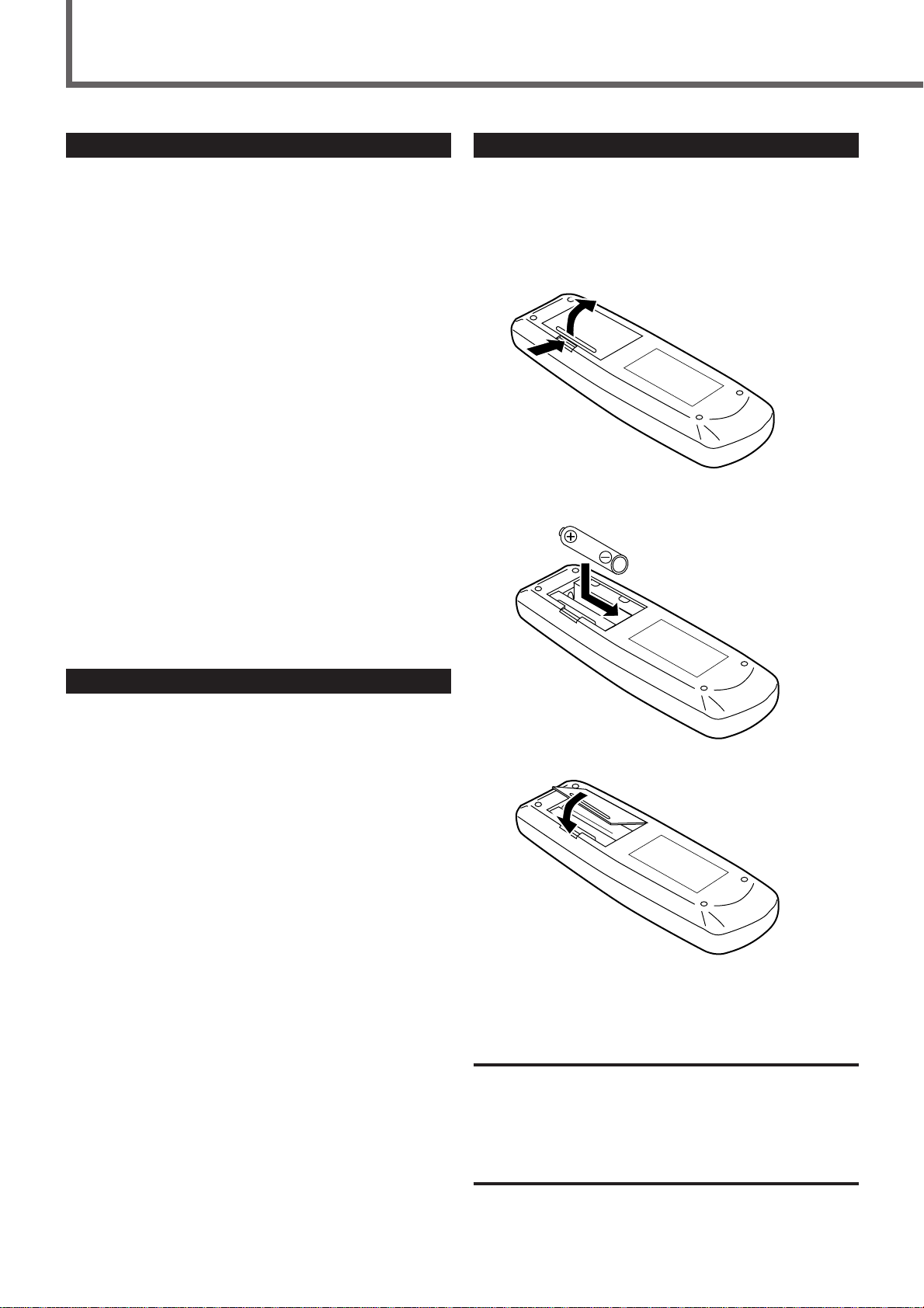
Getting Started
Before Installation
General Precautions
• DO NOT insert any metal object into the receiver.
• DO NOT disassemble the receiver or remove screws, covers, or
cabinet.
• DO NOT expose the receiver to rain or moisture.
Locations
• Install the receiver in a location that is level and protected from
moisture.
• The temperature around the receiver must be between 23˚F and
95˚F (–5˚C and 35˚C).
• Make sure there is good ventilation around the receiver. Poor
ventilation could cause overheating and damage the receiver.
Handling the receiver
• DO NOT touch the power cord with wet hands.
• DO NOT pull on the power cord to unplug the cord. When
unplugging the cord, always grasp the plug so as not to damage
the cord.
• Keep the power cord away from the connecting cords and the
antenna. The power cord may cause noise or screen interference. It
is recommended to use a coaxial cable for antenna connection,
since it is well-shielded against interference.
• When a power failure occurs, or when you unplug the power cord,
the preset settings such as preset FM/AM channels and sound
adjustments may be erased in a few days.
Putting Batteries in the Remote Control
Before using the remote control, put two supplied batteries first.
• When using the remote control, aim the remote control directly at
the remote sensor on the receiver.
1. On the back of the remote control, remove the
battery cover.
2
1
2. Insert batteries. Make sure to match the polarity:
(+) to (+) and (–) to (–).
Checking the Supplied Accessories
Check to be sure you have all of the following supplied accessories.
The number in the parentheses indicates the quantity of the pieces
supplied.
• Remote Control (1)
• Batteries (2)
• AM Loop Antenna (1)
• FM Antenna (1)
If anything is missing, contact your dealer immediately.
3. Replace the cover.
If the range or effectiveness of the remote control decreases, replace
the batteries. Use two R6P(SUM-3)/AA(15F) type dry-cell batteries.
CAUTION:
Follow these precautions to avoid leaking or cracking cells:
• Place batteries in the remote control so they match the polarity: (+)
to (+) and (–) to (–).
• Use the correct type of batteries. Batteries that look similar may
differ in voltage.
• Always replace both batteries at the same time.
• Do not expose batteries to heat or flame.
2
Page 51

Connecting the FM and AM Antennas
If AM reception is poor, connect single vinyl-covered wire (not supplied).
AM Loop Antenna
(supplied)
B
L
IA
FM 75
X
A
O
C
AM LOOP
If FM reception is poor, connect
outdoor FM antenna (not supplied).
FM 75
COAXIAL
FM Antenna (supplied)
Getting Started
Snap the tabs on the loop into
the slots of the base to
assemble the AM loop antenna.
1
2
3
AM
EXT
FM 75
ANTENNA
AM
AM
EXT
COAXIAL
LEFT
)
FRONT SPEAKERS
D
DIGITAL 1
V
D
(
LEFT
REAR SPEAKERS
RIGHT
RIGHT
+
+
–
–
DIGITAL IN
CENTER
)
DIGITAL 2
V
T
(
SPEAKER
+
–
OUT
AUDIO
P
O
LO
FM 75
ANTENNA
COAXIAL
LEFT
RIGHT
OUT
(REC)
DVD
IN
CD TV
(PLAY)
VCR
SUBWOOFER
AM antenna connection
Connect the AM loop antenna supplied to the AM LOOP
terminals.
Turn the loop until you have the best reception.
• If reception is poor, connect an outdoor single vinyl-covered
wire to the AM EXT terminal. (Keep the AM loop antenna
connected.)
+
CAUTION :
SPEAKER
6
IMPEDANCE
1
8
–
Notes:
• If the AM loop antenna wire is covered with vinyl,
remove the vinyl while twisting it as shown to the
right.
• Make sure the antenna conductors do not touch any
other terminals, connecting cords and power cord.
This could cause poor reception.
FM antenna connection
Connect the FM antenna supplied to the FM 75 Ω COAXIAL
terminal as temporary measure.
Extend the supplied FM antenna horizontally.
• If reception is poor, connect an outdoor antenna. Before
attaching a 75 Ω coaxial cable (with a standard type connector),
disconnect the supplied FM antenna.
3
Page 52

Getting Started
Connecting the Speakers
After connecting the front, center, rear speakers and/or a subwoofer,
set the speaker setting information properly to obtain the best
possible DSP effect. For details, see page 12.
CAUTION:
Use speakers with the SPEAKER IMPEDANCE indicated by the
speaker terminals.
Connecting the front, center, and rear speakers
Speaker Layout Diagram
ª
·
1
For each speaker, connect the (+) and (–) terminals on the rear panel
to the (+) and (–) terminals marked on the speakers respectively.
2
3
1 Cut, twist and remove the insulation at the end of
each speaker cord (not supplied).
2 Open the terminal, then insert the speaker cord.
3 Close the terminal.
Connecting the subwoofer
By connecting a subwoofer, you can enhance the bass or reproduce
the original LFE signals recorded in the digital software.
Powered subwoofer
(example)
SUBWOOFER
OUT
Right rear speaker
ª
·
INPUT
HIGH IMPEDANCE
Connect the input jack of a powered subwoofer to the
SUBWOOFER OUT jack on the rear panel, using a cable with RCA
pin plugs (not supplied).
• Refer also to the manual supplied for your subwoofer.
Since bass sound is non-directional, you can place a
subwoofer wherever you like. Normally place it in front of
you.
4
Page 53

Left rear speaker
Getting Started
To center speaker
To right front speaker
To right rear speaker
E
+
N
1
T
E
0
R
M
E
9
N
U
Center speaker
CENTER
SPEAKER
+
–
REAR SPEAKERS
RIGHT LEFT
FRONT SPEAKERS
+
+
–
–
RIGHT
LEFT
:
N
IO
T
U
R
A
E
+
C
K
E
A
C
E
N
P
A
S
D
E
P
IM
16
8
–
To left front speaker
To left rear speaker
Left front speaker
Right front speaker
RX-E100SL
AM LOOP
M
F
A
O
C
A
N
N
E
T
N
A
AM
EXT
S
R
E
K
A
E
P
T
F
S
N
E
1
I
L
L
L
T
A
A
N
T
T
T
I
O
I
H
R
)
G
G
I
G
I
F
I
+
CAUTION :
D
D
R
D
V
D
S
(
R
SPEAKER
E
K
A
E
6
IMPEDANCE
P
1
S
T
R
F
8
A
E
E
L
–
R
+
T
H
G
I
2
R
R
E
L
+
T
A
N
T
I
E
R
E
C
IG
)
K
D
V
A
E
T
(
P
S
–
–
+
–
FER
O
O
T
U
UBW
O
O
I
D
U
A
75
L
IA
X
T
F
E
L
TV
IN
T
H
G
I
R
(PLAY)
OUT
(REC)
CR CD
V
S
D
V
D
5
Page 54

Getting Started
Connecting Audio/Video Components
Connecting cords are not supplied with this unit. Use the
cords supplied for the other components or purchase them at
an audio or electric appliance store.
A
Optical digital cord
B
Coaxial digital cord
C
Audio cord
RX-E100SL
Turn the power off to all components before connections.
Digital connections
DIGITAL IN
DIGITAL 2
(TV)
Before connecting an
optical digital cord, unplug
the protective plug.
DIGITAL 1
(DVD)
LEFT
)
FRONT SPEAKERS
D
DIGITAL 1
V
D
(
LEFT
REAR SPEAKERS
RIGHT
RIGHT
+
+
–
–
DIGITAL IN
CENTER
)
DIGITAL 2
V
T
(
SPEAKER
+
–
OUT
AUDIO
AM LOOP
FM 75
COAXIAL
LEFT
ANTENNA
AM
EXT
RIGHT
OUT
(REC)
DVD
IN
CD TV
(PLAY)
VCR
SUBWOOFER
If you connect a sound-enhancing device such as a
graphic equalizer between the source components and
this receiver, the sound output through this receiver may
be distorted.
Connecting the Power Cord
Before plugging the receiver into an AC outlet, make sure that all
connections have been made.
Analog
+
CAUTION :
SPEAKER
6
IMPEDANCE
1
8
–
connections
LEFT
RIGHT
OUT
(REC)
VCR
IN
(PLAY)
AUDIO
CD TV DVD
Plug the power cord into an AC outlet.
6
Page 55
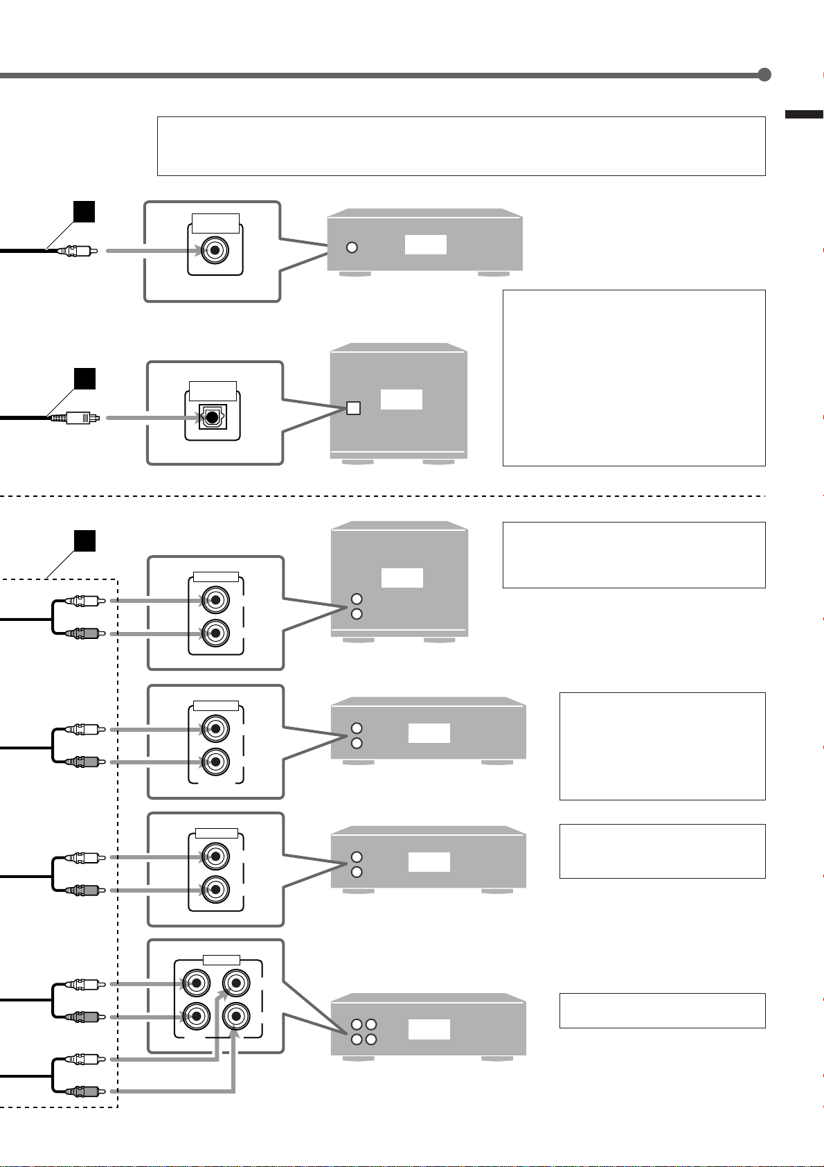
Illustrations of the input/output terminals below are typical examples.
When you connect other components, refer also to their manuals since the terminal names actually printed
on the rear vary among the components.
Getting Started
A
COAXIAL
DIGITAL OUT
DVD
• When shipped from the factory, the DIGITAL IN
terminals have been set for use with the
following components.
– DIGITAL 1 (coaxial): For DVD player
– DIGITAL 2 (optical): For digital TV tuner
B
OPTICAL
DIGITAL OUT
TV
C
AUDIO OUT
LEFT
TV
If you connect other components, change the
digital input (DIGITAL IN) terminal setting
correctly. See “Setting the Digital Input
Terminals” on page 10.
• Select the digital input mode correctly.
See “Selecting the Analog or Digital Input
Mode” on page 11.
• Connect the video input directly to the video
output on the DVD player and/or VCR.
• You can also connect the digital TV tuner using
the optical digital cable (see above).
AUDIO OUT
FRONT/MIX
LINE OUT
AUDIO
OUT IN
RIGHT
LEFT
RIGHT
LEFT
RIGHT
LEFT
RIGHT
DVD
CD
VCR
• Connect the video out directly to the
video input on the TV.
• To enjoy the software encoded with
Dolby Digital or DTS Digital
Surround, connect the DVD player
using one of the DIGITAL IN
terminals (see above).
You can also connect the CD player
using one of the DIGITAL IN terminals
(see above).
Connect the video out directly to the
video input on the TV.
7
Page 56

Basic Operations
This manual mainly explains operations using the buttons and controls on the front panel. You can also use the buttons on the remote
control if they have the similar names (or marks) as those on the front panel.
If operations using the remote control are different from those using the front panel, they are then explained.
• You can also see “Mastering Remote Operations” on page 32.
STANDBY lamp
STANDBY
POWER
DIGITAL
SURROUND
TV DILECT
SETTING
DIGITAL
ADJUST
CONTROL
ANALOG
LCR
LPCM
SUBWFR LFE
DOLBY D
LS S RS
DTS
MEMORY
DVD
DVD TV VCR CD FM
123
1
Turn On the Power
Press POWER (or AUDIO of the POWER buttons on the remote
control).
The STANDBY lamp goes off. The name of the
current source (or station frequency) appears on
the display.
Current volume level is shown here
LR
LPCM
DGTL AUTO
Current source name appears
STANDBY
POWER
VOL
Display
HOME THEATER RECEIVER
RX-E100
PRO LOGIC
SLEEP STTUNED MUTING
DSP
DGTL AUTO
INPUT ATT
Note:
When you have connected some digital source components using the
digital terminals (see page 6), see “Basic Settings” on pages 10 and
11 to finish the digital input terminal setting and digital input mode
setting correctly before use.
3
To increase the volume, press and hold
MASTER VOLUME (or VOLUME + on the
remote control).
To decrease the volume, press and hold
MASTER VOLUME
remote control).
AUTO
MH
Z
KHZ
VOL
AM
INPUT
ANALOG/DIGITAL
INPUT ATT
SURROUND
ON/OFF
DSP
MODE
MASTER V OLUME
Adjust the Volume
(or VOLUME – on the
MASTER VOLUME
To turn off the power (into standby)
Press POWER (or AUDIO) again.
The STANDBY lamp lights up.
A small amount of power is consumed in standby
mode. To turn the power off completely, unplug
the AC power cord.
2
Select the Source to Play
Press one of the source selecting buttons.
DVD
DVD TV VCR CD FM
DVD :Select the DVD player.
TV : Select the TV sound.
VCR : Select the VCR.
CD : Select the CD player.
FM : Select an FM broadcast.
AM : Select an AM broadcast.
STANDBY
POWER
AM
CAUTION:
Always set the volume to the minimum before starting any source. If
the volume is set at its high level, the sudden blast of sound energy
can permanently damage your hearing and/or ruin your speakers.
Notes:
• The volume level can be adjusted within the range of “0” (minimum)
to “70” (maximum).
• Each time you press the button, the volume level changes by 2
steps from “0” (minimum) to “14” and by 1 step from “14” to “70”
(maximum).
8
Page 57

To turn off the sounds temporarily
T
Press MUTING on the remote control to mute
the sound through all speakers connected.
MUTING
O
“MUTING” appears on the display and the volume
turns off (the volume level indicator goes off).
To restore the sound, press MUTING again so that “MUTING
OFF” appears on the display.
• Pressing MASTER VOLUME
/ (or VOLUME +/–) also
restores the sound.
Turning Off the Power
with the Timer
You can fall asleep while listening to music — Sleep Timer.
Press SLEEP
The SLEEP indicator lights up on the display, and the shut-off time
changes in 10 minute intervals.
on the remote control repeatedly.
SLEEP
LPCM
LR
SLEEP
DGTL AUTO
Remote
ONLY
Remote
ONLY
VOL
2010 30 40 50 60 70 80 90
0
(Canceled)
Basic adjustment auto memory
This receiver memorizes sound settings for each source ....
• when you turn on the power,
• when you change the source, and
• when you change the analog/digital input mode (see page 11).
When you change the source, the memorized settings for the
newly selected source are automatically recalled.
The following can be stored for each source:
• Analog/digital input mode (see page 11)
• Input attenuator mode (see page 17)
• Balance (see page 17)
• Bass boost (see page 18)
• Tone adjustment (see page 19)
• Subwoofer output level (see page 19)
• Surround mode settings (see pages 25, 29)
Theater Surround settings (see pages 27, 30)
DAP mode settings (see pages 28, 31)
Note:
If the source is FM or AM, you can assign a different setting for
each band.
For recording
You can record sounds of any source playing through the receiver
to the VCR connected to the VCR jacks.
While recording, you can listen to the selected sound source at
whatever sound level you like without affecting the sound levels
of the recording.
Note:
Sound adjustments (see page 17) and DSP modes (see page 22)
cannot affect the recording.
Basic Operations
When the shut-off time comes
The receiver turns off automatically.
To check or change the time remaining until the shut-off time
Press SLEEP once.
The remaining time (in minutes) until the shut-off time appears.
• To change the shut-off time, press SLEEP repeatedly.
To cancel the Sleep Timer
Press SLEEP repeatedly until “SLEEP 0” appears on the display.
(The SLEEP indicator goes off.)
• Turning off the power also cancels the Sleep Timer.
Signal and speaker indicators on the display
LCR
LFE
LS S RS
ANALOG
LPCM
DOLBY D
DTS
LCR
SUBWFR LFE
LS S RS
PRO LOGIC
DSP
DGTL AUTO
INPUT ATT
Signal indicators
The following signal indicators light up —:
L:•When digital input is selected: Lights up when the
left channel signal comes in.
• When analog input is selected: Al ways lights up.
R:•When digital input is selected: Lights up when the
right channel signal comes in.
• When analog input is selected: Al ways lights up.
C: Lights up when the center channel signal comes in.
LS: Lights up when the left rear channel signal comes in.
RS: Lights up when the right rear channel signal comes in.
S: Lights up when the monaural rear channel signal comes in.
LFE: Lights up when the LFE channel signal comes in.
The speaker indicators light up as follows:
• The subwoofer speaker indicator (
SUBWFR) lights up when
“SUBWFR” is set to “YES” (see page 12).
• The other speaker indicators light up only when the
corresponding speaker is activated AND when the
corresponding speaker is required for the DSP mode currently
selected.
LCR
SLEEP
SUBWFR
LS RS
Speaker indicators
9
Page 58

Basic Settings
(back to the begining)
ANALOG
PRO LOGIC
SUBWFR LFE
VOL
DGTL AUTO
INPUT ATT
DSP
LCR
LS S RS
LPCM
DOLBY D
DTS
CONTROL
5/∞/3/2
Display
STANDBY
POWER
TV DILECT
ADJUST
SETTING
DIGITAL
DIGITAL
SURROUND
SETTING
CONTROL
RX-E100
PRO LOGIC
ANALOG
LCR
DSP
LPCM
SUBWFR LFE
DGTL AUTO
DOLBY D
LS S RS
INPUT ATT
MEMORY
DTS
DVD
DVD TV VCR CD FM
Source selecting buttons
(DVD, TV, CD)
Setting the Digital Input
Terminals
Remote
NOT
When you use the digital input terminals, register what components
are connected to which terminals (DIGITAL IN 1/2) so that the
correct source name will appear when you select the digital source.
Before you start, remember...
There is a time limit in doing the following steps. If the setting is
canceled before you finish, start from step 1 again.
1
Press SETTING.
SETTING
The CONTROL buttons now work for basic
settings.
HOME THEATER RECEIVER
SLEEP STTUNED MUTING
AUTO
3
Press CONTROL 3 (or 2) to select the
appropriate digital terminal setting.
• Each time you press the button, the display changes to show
the following:
Z
MH
KH
Z
VOL
AM
INPUT
ANALOG/DIGITAL
INPUT ATT
SURROUND
ON/OFF
INPUT
ANALOG/DIGITAL
CONTROL
DSP
MODE
MASTER V OLUME
2
Press CONTROL ∞ (or 5) repeatedly until
“DGT (Digital)” (with the current setting)
appears on the display.
CONTROL
* “1DVD2TV” is the initial setting. If you have already changed
the setting, another combination will be shown.
Note:
*
When shipped from the factory, the DIGITAL IN terminals have been
set for use with the following components.
• DIGITAL 1 (coaxial): For DVD player
• DIGITAL 2 (optical): For digital TV tuner
VOL
10
Page 59

N
Selecting the Analog or Digital Input Mode
SUBWFR LFE
MU
MH
KH
VO
DGTL AUTO
LCR
LS RS
DOLBY D
When you have connected digital source components using both the
analog connection and the digital connection methods (see page 6),
you need to select the input mode correctly.
1
Press one of the source selecting buttons (DVD,
TV, or CD)* for which you want to change the
input mode.
DVD
DVD TV VCR CD
Note:
*
Among the sources listed above, you can select the digital input
only for the sources which you have selected the digital input
terminals for. (See “Setting the Digital Input Terminals” on page
10.)
2
Press INPUT ANALOG/DIGITAL (or INPUT A/
D on the remote control) to select the analog or
digital input mode.
• Each time you press the button, the input mode alternates
between the analog input (ANALOG) and the digital input
(DGTL AUTO).
INPUT
ANALOG/DIGITAL
INPUT ATT
If the following symptoms occur while playing Dolby Digital or
DTS Digital Surround software with “DGTL AUTO” selected,
follow the procedure below.
• Sound does not come out at the beginning of playback.
• Noise comes out while searching or skipping chapters or tracks.
1
Press one of the source selecting buttons (DVD, TV, or CD) for
which you want to change the input mode.
DVD
DVD TV VCR CD
2
Press INPUT ANALOG/DIGITAL (or INPUT A/D) to select the
digital input mode (DGTL AUTO).
INPUT
ANALOG/DIGITAL
INPUT ATT
3
Press CONTROL 3 (or 2) to select “DGTL
D.D.” or “DGTL DTS” while “DGTL AUTO”
still remains on the display.
Remote
NOT
• Each time you press the button, the digital input mode changes
as follows:
CONTROL
When “DGTL D.D.” or “DGTL DTS” is
selected, “AUTO” goes off.
Basic Settings
LCR
SUBWFR LFE
LS RS
DGTL AUTO
DOLBY D
DGTL AUTO : Select this for the digital input mode. The
receiver automatically detects the incoming
signal format. (The DGTL AUTO indicator
lights up on the display, then the digital signal
indicator for the detected signals lights up.)
ANALOG : Select this for the analog input mode. (Initial
setting when shipped from the factory)
MUTI
MH
Z
KH
Z
VOL
• To play back software encoded with Dolby Digital, select
“DGTL D.D.”
• To play back software encoded with DTS Digital Surround,
select “DGTL DTS.”
Note:
When you turn off the power or select another source, “DGTL DTS”
and “DGTL D.D.” are canceled and the digital input mode is
automatically reset to “DGTL AUTO.”
The following are the analog/digital signal indicators on the display
to indicate what type of the signal comes into the receiver.
ANALOG : Lights when the analog input is selected.
LPCM :Lights when Linear PCM signals come in.
DOLBY D : •Lights when Dolby Digital signals come in.
•Flashes when “DGTL D.D.” is selected for
software not encoded with Dolby Digital.
DTS : •Lights when DTS Digital Surround signals come
in.
•Flashes when “DGTL DTS” is selected for
software not encoded with DTS Digital Surround.
Note:
When “DGTL AUTO” cannot recognize the incoming signals, no digital
signal indicators light up on the display.
11
Page 60
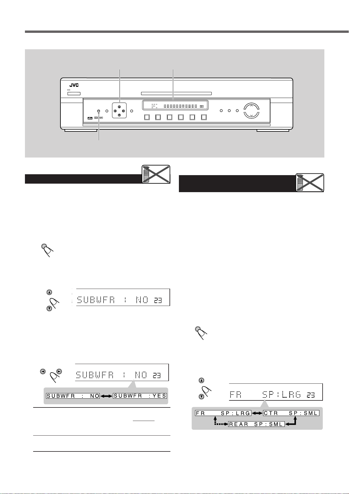
Basic Settings
CONTROL
STANDBY
POWER
DIGITAL
SURROUND
TV DILECT
SETTING
DIGITAL
5/∞/3/2
CONTROL
ADJUST
MEMORY
DVD
DVD TV VCR CD FM
RX-E100
PRO LOGIC
ANALOG
LCR
DSP
LPCM
SUBWFR LFE
DGTL AUTO
DOLBY D
LS S RS
INPUT ATT
DTS
Display
SLEEP STTUNED MUTING
SETTING
Remote
Setting the Subwoofer Information
NOT
When you have connected a subwoofer, follow the procedure below.
If you do not use a subwoofer, you can skip this setting.
Before you start, remember...
There is a time limit in doing the following steps. If the setting is
canceled before you finish, start from step 1 again.
1
Press SETTING.
SETTING
The CONTROL buttons now work for basic
settings.
HOME THEATER RECEIVER
AUTO
MHZ
KHZ
VOL
AM
INPUT
ANALOG/DIGITAL
INPUT ATT
SURROUND
ON/OFF
DSP
MODE
MASTER V OLUME
Setting the Speakers for
DSP Modes
To obtain the best possible surround effect from the DSP (Digital
Signal Processor) modes (see page 22), register the following
information after all connections are completed.
• Speaker Size — FR SP, CTR SP, REAR SP
• Delay Time — CTR DL, REAR DL
• Crossover Frequency — CROSS
• Dynamic Range Compression — D.R.C.
• Low Frequency Effect Attenuator — LFE
Remote
NOT
2
Press CONTROL ∞ (or 5) repeatedly until
“SUBWFR (Subwoofer)” (with the current
setting)
* “NO” is the initial setting. If you have already changed the
3
Press CONTROL 3 (or 2) to select “YES.”
• Each time you press the button, the subwoofer setting
YES : Select this when a subwoofer is used.
NO : Select this when you have not connected or have
* appears on the display.
CONTROL
IC
TO
T
setting, “YES” will be shown.
alternates between “YES” and “NO.”
CONTROL
LCR
SUBWFR LFE
LS S RS
PRO LOGIC
DSP
DGTL AUTO
INPUT ATT
ANALOG
LPCM
DOLBY D
DTS
The subwoofer speaker indicator (
up on the display (see page 9). You can adjust the
subwoofer output level (see page 19).
disconnected a subwoofer.
SUBWFR) lights
Speaker Size — FR SP, CTR SP, REAR SP
Register the sizes of all the connected speakers.
• When you change your speakers, register the information about
the speakers again.
Before you start, remember...
VOL
There is a time limit in doing the following steps. If the setting is
canceled before you finish, start from step 1 again.
1
Press SETTING.
SETTING
The CONTROL buttons now work for basic
settings.
2
Press CONTROL ∞ (or 5) repeatedly until one
of the following speakers (with the current
CONTROL
ANALOG
LPCM
DOLBY D
DTS
SUBWFR LFE
LS S RS
* appears.
PRO LOGIC
LCR
DSP
DGTL AUTO
INPUT ATT
VOL
setting)
VOL
12
Page 61
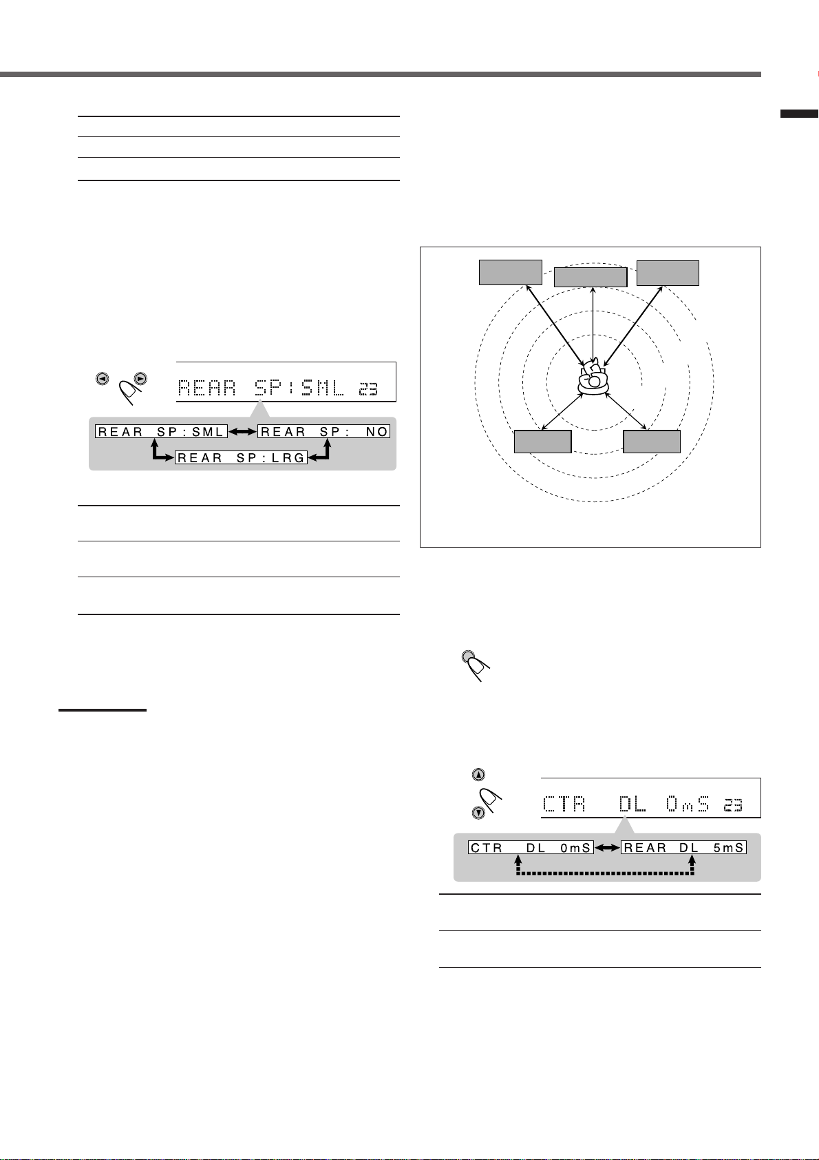
FR SP (Front Speaker) : To register the front speaker size.
ANALOG
PRO LOGIC
SUBWFR LFE
VOL
DGTL AUTO
INPUT ATT
DSP
LCR
LS S RS
LPCM
DOLBY D
DTS
SETTING
CTR SP (Center Speaker) : To register the center speaker size.
REAR SP (Rear Speaker) : To register the rear speaker size.
* “LRG (large)” is the initial setting for the front speakers, and
“SML (small)” is for the center and rear speakers.
If you have already changed the setting, another size will be
shown.
3
Press CONTROL 3 (or 2) to select the
appropriate speaker size.
• Each time you press the button, the speaker size changes as
follows:
CONTROL
LCR
SUBWFR LFE
LS S RS
PRO LOGIC
DSP
DGTL AUTO
INPUT ATT
ANALOG
LPCM
DOLBY D
DTS
Delay Time — CTR DL, REAR DL
Basic Settings
Adjust the delay time of the sounds from the center speaker and
from the rear speakers, comparing to that of the sounds from the
front speakers. If the distance to the center speaker and/or the rear
speakers from your listening point is almost the same as that to the
front speakers, select 0 msec.
• 1 msec increase (or decrease) in delay time corresponds to 1 foot
(30 cm) increase (or decrease) in distance.
Left front
speaker
VOL
Center speaker
7 feet
(2.1 m)
Right front
speaker
(2.7 m)
8 feet
(2.4 m)
9 feet
10 feet
(3.0 m)
Ex.: When registering the rear speaker size
LRG (Large) : Select this when the speaker size is relatively
large. (See “Notes” below.)
SML (Small) : Select this when the speaker size is relatively
small. (See “Notes” below.)
NO : Select this when you have not connected a
speaker. (Not selectab le for the front speakers)
4
Repeat steps 2 and 3 to select the appropriate
size for the other speakers.
Notes:
• Use the following criteria as reference when adjusting:
– If the size of the cone speaker unit built in your speaker is greater
than 4 3/4 inches (12 cm ), select “LRG (large),” and if it is smaller
than 4 3/4 inches (12 cm ), select “SML (small).”
• If you have selected “NO” for the subwoofer, you can only select
“LRG (large)” for the front speaker size.
• If you have selected “SML (small)” for the front speaker size, you
cannot select “LRG (large)” for the center and rear speaker sizes.
Left rear
speaker
Right rear
speaker
Ex.: In this case, set the center delay to “1 mS” and the
rear delay to “2 mS.”
Before you start, remember...
There is a time limit in doing the following steps. If the setting is
canceled before you finish, start from step 1 again.
1
Press SETTING.
The CONTROL buttons now work for basic
settings.
2
Press CONTROL ∞ (or 5) repeatedly until
“CTR DL (Center Delay)” or “REAR DL (Rear
Delay” (with the current setting)
* appears on the
display.
CONTROL
CTR DL (Center Delay) : To adjust the center delay time
(from 0 msec to 5 msec).
REAR DL (Rear Delay) : To adjust the rear delay time
(from 0 msec to 15 msec).
* “0 mS (msec)” is the initial setting for the center delay time
and
“5 mS (msec)” for the rear delay time. If you have already
changed the setting, another setting will be shown.
TO BE CONTINUED TO THE NEXT PAGE
13
Page 62

Basic Settings
ANALOG
PRO LOGIC
SUBWFR LFE
VOL
DGTL AUTO
INPUT ATT
DSP
LCR
LS S RS
LPCM
DOLBY D
DTS
CONTROL
5/∞/3/2
STANDBY
POWER
DIGITAL
SURROUND
TV DILECT
SETTING
DIGITAL
ADJUST
CONTROL
MEMORY
SETTING
3
Press CONTROL 3 (or 2) to select the delay
time.
• Each time you press the button, the delay time changes by
“1 mS (msec).”
CONTROL
LCR
SUBWFR LFE
LS S RS
PRO LOGIC
DSP
DGTL AUTO
INPUT ATT
ANALOG
LPCM
DOLBY D
DTS
Display
HOME THEATER RECEIVER
RX-E100
PRO LOGIC
ANALOG
SLEEP STTUNED MUTING
LCR
DSP
LPCM
SUBWFR LFE
DGTL AUTO
DOLBY D
LS S RS
INPUT ATT
DTS
DVD
DVD TV VCR CD FM
2
Press CONTROL ∞ (or 5) repeatedly until
“CROSS (Crossover)” (with the current setting)
appears on the display.
VOL
AUTO
Z
MH
KH
Z
VOL
CONTROL
SURROUND
DSP
INPUT
ON/OFF
INPUT ATT
MODE
MASTER V OLUME
ANALOG/DIGITAL
AM
*
IC
TO
T
VOL
Ex.: When adjusting the center delay
4
Repeat steps 2 and 3 to adjust the other delay
time.
Crossover Frequency — CROSS
Small speakers cannot reproduce the bass sounds efficiently. If you
use a small speaker in any position, this receiver automatically
reallocates the bass sound elements assigned to the small speaker to
large speakers.
To use this function properly, set this crossover frequency level
according to the size of the small speaker connected.
• If you have selected “LRG (large)” for all speakers, this function
will not take effect.
Before you start, remember...
There is a time limit in doing the following steps. If the setting is
canceled before you finish, start from step 1 again.
1
Press SETTING.
SETTING
The CONTROL buttons now work for basic
settings.
* “100HZ” is the initial setting. If you have already changed the
setting, another frequency will be shown.
3
Press CONTROL 3 (or 2) to select the crossover
frequency level.
• Each time you press the button, the crossover frequency level
changes as follows:
CONTROL
• Use the following criteria as reference when adjusting:
80HZ: Select this frequency when the cone speaker unit
built in the speaker is about 4
100HZ: Select this frequency when the cone speaker unit built
in the speaker is about 3
120HZ: Select this frequency when the cone speaker unit
built in the speaker is about 3 3/16 inches (8 cm).
3
/4 inches (12 cm).
15
/16 inches (10 cm).
14
Page 63

O
Dynamic Range Compression — D.R.C.
T
ANALOG
PRO LOGIC
SUBWFR LFE
VOL
DGTL AUTO
INPUT ATT
DSP
LCR
LS S RS
LPCM
DOLBY D
DTS
You can compress the dynamic range (difference between maximum
sound and minimum sound) of the reproduced sound. This is useful
when enjoying surround sound at night.
• This function takes effect only when playing back a source using
Dolby Digital.
Before you start, remember...
There is a time limit in doing the following steps. If the setting is
canceled before you finish, start from step 1 again.
1
Press SETTING.
SETTING
2
Press CONTROL∞ (or 5) repeatedly until
The CONTROL buttons now work for basic
settings.
“D.R.C. (Dynamic Range Compression)” (with
the current setting)
* appears on the display.
Low Frequency Effect Attenuator — LFE
If the bass sound is distorted while playing back software using
Dolby Digital or DTS Digital Surround, follow the procedure below.
• This function takes effect only when the subwoofer (LFE) signals
come in, (with “SUBWFR” set to “YES”).
Before you start, remember...
There is a time limit in doing the following steps. If the setting is
canceled before you finish, start from step 1 again.
1
Press SETTING.
SETTING
The CONTROL buttons now work for basic
settings.
2
Press CONTROL ∞ (or 5) repeatedly until “LFE
(Low Frequency Effect)” (with the current
setting)
* appears on the display.
CONTROL
Basic Settings
CONTROL
IC
O
* “MID” is the initial setting. If you have already changed the
setting, another setting will be shown.
3
Press CONTROL 3 (or 2) to select the
appropriate compression level.
• Each time you press the button, the compression level changes
as follows:
CONTROL
ANALOG
LPCM
DOLBY D
DTS
OFF : Select this when you want to enjoy surround with its
MID : Select this when you want to reduce the dynamic range
MAX :Select this when you want to apply the compression
PRO LOGIC
LCR
DSP
SUBWFR LFE
DGTL AUTO
LS S RS
INPUT ATT
full dynamic range. (No effect applied.)
a little.
effect fully. (Useful at night.)
VOL
VOL
* “0” is the initial setting. If you have already changed the
setting, “–10dB” will be shown.
3
Press CONTROL 3 (or 2) to select the LFE
attenuator level.
• Each time you press the button, the LFE attenuator level
changes as follows:
CONTROL
VOL
0dB : Normally select this.
–10dB : Select this when the bass sound is distorted.
15
Page 64
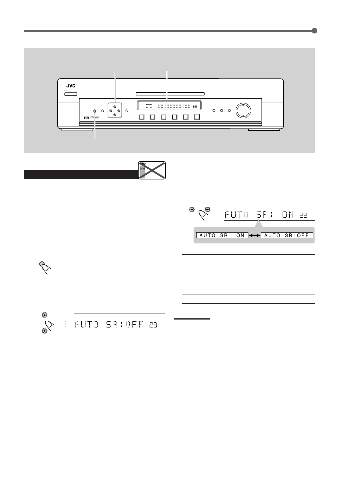
Basic Settings
CONTROL
5/∞/3/2
STANDBY
POWER
DIGITAL
SURROUND
TV DILECT
SETTING
DIGITAL
ADJUST
CONTROL
ANALOG
LCR
LPCM
SUBWFR LFE
DOLBY D
LS S RS
MEMORY
DTS
DVD
DVD TV VCR CD FM
RX-E100
PRO LOGIC
DSP
DGTL AUTO
INPUT ATT
SETTING
Remote
Setting Auto Surround
NOT
Surround mode is automatically activated when a multichannel
digital signal comes into this receiver through the digital terminal.
You can enjoy Surround mode simply by selecting the source (with
digital input selected for that source) — Auto Surround.
To activate Auto Surround, follow the procedure below.
Before you start, remember...
There is a time limit in doing the following steps. If the setting is
canceled before you finish, start from step 1 again.
Display
HOME THEATER RECEIVER
SLEEP STTUNED MUTING
AUTO
3
Press CONTROL 3 (or 2) to select “ON.”
• Each time you press the button, Auto Surround turns “ON” or
“OFF.”
Z
MH
KH
Z
VOL
CONTROL
ANALOG
LPCM
DOLBY D
DTS
AM
LCR
SUBWFR LFE
LS S RS
INPUT
ANALOG/DIGITAL
INPUT ATT
PRO LOGIC
DSP
DGTL AUTO
INPUT ATT
SURROUND
ON/OFF
DSP
MODE
MASTER V OLUME
VOL
1
Press SETTING.
SETTING
The CONTROL buttons now work for basic
settings.
2
Press CONTROL ∞ (or 5) repeatedly until
“AUTO SR (Auto Surround)” (with the current
setting)
* “OFF” is the initial setting. If you have already changed the
* appears on the display.
CONTROL
LOGIC
L AUTO
UT ATT
setting, “ON” will be shown.
ON : • If multichannel signals come in, an appropriate
Surround mode will be turned on
• If Dolby Digital 2 channel or DTS 2 channel
signals come in, “STEREO” will be selected.
• If linear PCM signals come in, nothing will
change.
OFF : Select this to deactivate Auto Surround.
Notes:
VOL
• This function does not take effect in the following cases:
– While playing an analog source.
– While selecting “DGTL DTS” or “DGTL D.D.” as the fixed digital
input mode (see page 11).
• If Surround mode is automatically activated by Auto Surround,
another DSP mode in use will be canceled temporarily. When
multichannel digital signals stop coming in, the selected surround
mode is canceled, and the previous DSP mode resumes.
• If you press SURROUND ON/OFF (SURROUND on the remote
control) or DSP MODE with Auto Surround activated, Auto
Surround will be canceled temporarily for the currently selected
source.
Auto Surround setting will be restored in the following cases.
– When you turn off and on the unit,
– When you change the source, and
– When you reset “AUTO SR” to “ON” again.
16
To cancel Auto Surround
Repeat step 1 and 2, then select “OFF” in step 3.
Page 65

Sound Adjustments
N
T
You can also use the remote control for some sound adjustments.
• When using the remote control, see also “Mastering Remote Operations” on page 32.
CONTROL
5/∞/3/2
Display
INPUT ATT
Basic Settings/Sound Adjustments
STANDBY
POWER
DIGITAL
SURROUND
TV DILECT
SETTING
DIGITAL
ADJUST
CONTROL
ANALOG
LCR
LPCM
SUBWFR LFE
DOLBY D
LS S RS
MEMORY
DTS
DVD
DVD TV VCR CD FM
RX-E100
PRO LOGIC
DSP
DGTL AUTO
INPUT ATT
ADJUST
Remote
Attenuating the Input Signal
NOT
When the input level of the analog source is too high, the sounds
will be distorted. If this happens, you need to attenuate the input
signal level to prevent the sound distortion.
• You have to make this adjustment for each analog source.
Press and hold INPUT ATT (INPUT ANALOG/DIGITAL) so
that the INPUT ATT indicator lights up on the display.
• Each time you press and hold the button, the Input Attenuator
turns on (“ATT ON”) or off (“ATT NORMAL”).
INPUT
ANALOG/DIGITAL
INPUT ATT
ANALOG
LR
INPUT ATT
ATT ON
ATT NORMAL
HOME THEATER RECEIVER
SLEEP STTUNED MUTING
AUTO
2
Press CONTROL ∞ (or 5) repeatedly until
“BAL (Balance)” (with the current setting)
appears on the display.
CONTROL
* “CENTER” is the initial setting. If you have already changed
the setting, another setting will be shown.
3
Press CONTROL 3 or 2 to adjust the front
speaker balance.
MUTI
MH
Z
KH
Z
VOL
CONTROL
ANALOG
LPCM
DOLBY D
DTS
Z
MH
KH
Z
VOL
LCR
SUBWFR LFE
LS S RS
SURROUND
DSP
INPUT
ON/OFF
ANALOG/DIGITAL
INPUT ATT
AM
MODE
MASTER V OLUME
*
IC
PRO LOGIC
DSP
DGTL AUTO
INPUT ATT
O
VOL
VOL
Adjusting the Front Speaker
Output Balance
If the sounds you hear from the front right and left speakers are
unequal, you can adjust the speaker output balance.
• You have to make this adjustment for each source.
Remote
NOT
• Pressing CONTROL 3 decreases the left channel output
(from CENTER to L–21).
• Pressing CONTROL 2 decreases the right
channel output (from CENTER to R–21).
Before you start, remember...
There is a time limit in doing the following steps. If the setting is
canceled before you finish, start from step 1 again.
1
Press ADJUST .
ADJUST
The CONTROL buttons now work for sound
adjustments.
17
Page 66
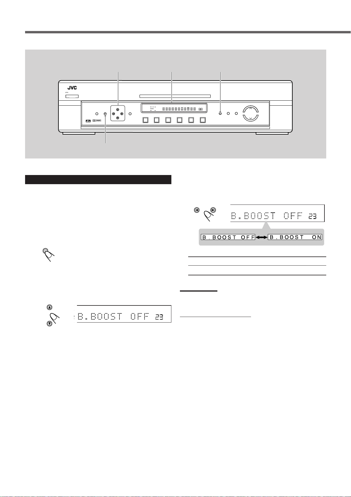
Sound Adjustments
CONTROL
5/∞/3/2
Display
INPUT ATT
STANDBY
POWER
DIGITAL
SURROUND
TV DILECT
SETTING
DIGITAL
ADJUST
CONTROL
ANALOG
LCR
LPCM
SUBWFR LFE
DOLBY D
LS S RS
MEMORY
DTS
DVD
DVD TV VCR CD FM
RX-E100
PRO LOGIC
DSP
DGTL AUTO
INPUT ATT
ADJUST
Reinforcing the Bass
You can boost the bass level — Bass Boost.
• You have to make this adjustment for each source.
Before you start, remember...
There is a time limit in doing the following steps. If the setting is
canceled before you finish, start from step 1 again.
1
Press ADJUST .
ADJUST
The CONTROL buttons now work for sound
adjustments.
2
Press CONTROL ∞ (or 5) repeatedly until “B.
BOOST (Bass Boost)” (with the current setting)
appears on the display.
CONTROL
C
O
* “OFF” is the initial setting. If you have already changed the
setting, “ON” will be shown.
VOL
HOME THEATER RECEIVER
SLEEP STTUNED MUTING
AUTO
Z
MH
KH
Z
VOL
AM
3
Press CONTROL 3 (or 2) to turn “ON” or
INPUT
ANALOG/DIGITAL
INPUT ATT
SURROUND
ON/OFF
DSP
MODE
MASTER V OLUME
“OFF” Bass Boost.
CONTROL
LCR
SUBWFR LFE
LS S RS
PRO LOGIC
DSP
DGTL AUTO
INPUT ATT
ANALOG
LPCM
DOLBY D
DTS
ON : Select this to boost the bass level. (Bass Boost)
OFF : Select this to deactivate Bass Boost.
*
Note:
This function affects the sound outputting only through the front
speakers.
When using the remote control
1
Press SOUND.
10 keys now work for sound adjustments.
2
Press BASS BOOST.
• Each time you press the button, Bass Boost turns on and off
alternately.
VOL
18
Page 67
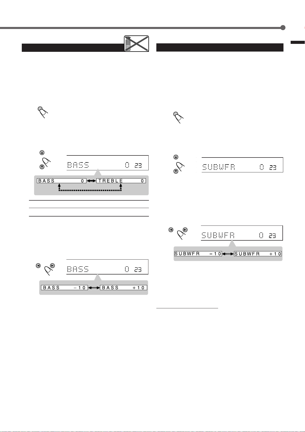
Adjusting the Tone
ANALOG
PRO LOGIC
SUBWFR LFE
VOL
DGTL AUTO
INPUT ATT
DSP
LCR
LS S RS
LPCM
DOLBY D
DTS
Remote
NOT
Adjusting the Subwoofer Output Level
Sound Adjustments
You can adjust the bass and treble sounds as you like.
• You have to make these adjustments for each source.
Before you start, remember...
There is a time limit in doing the following steps. If the setting is
canceled before you finish, start from step 1 again.
1
Press ADJUST .
ADJUST
The CONTROL buttons now work for sound
adjustments.
2
Press CONTROL ∞ (or 5) repeatedly until
“BASS” or “TREBLE” (with the current
setting)
BASS : To adjust the bass.
TREBLE :To adjust the treble.
* “0” is the initial setting. If you have already changed the
* appears.
CONTROL
LCR
SUBWFR LFE
LS S RS
PRO LOGIC
DSP
DGTL AUTO
INPUT ATT
ANALOG
LPCM
DOLBY D
DTS
setting, another number (level) will be shown.
VOL
You can adjust the subwoofer output level if you have connected a
subwoofer and set the subwoofer information correctly – “YES.”
• You have to make this adjustment for each source.
Before you start, remember...
There is a time limit in doing the following steps. If the setting is
canceled before you finish, start from step 1 again.
1
Press ADJUST .
ADJUST
The CONTROL buttons now work for sound
adjustments.
2
Press CONTROL ∞ (or 5) repeatedly until
“SUBWFR (subwoofer)” (with the current
setting)
* “0” is the initial setting. If you have already changed the
3
Press CONTROL 3 or 2 to adjust the sound
* appears.
CONTROL
OGIC
AUTO
ATT
setting, another number (level) will be shown.
VOL
output level.
CONTROL
3
Press CONTROL 3 or 2 to adjust the sound
level.
CONTROL
LCR
SUBWFR LFE
LS S RS
PRO LOGIC
DSP
DGTL AUTO
INPUT ATT
ANALOG
LPCM
DOLBY D
DTS
Ex.: When adjusting the bass level
• Pressing CONTROL 3 increases the sound level by +2 steps
(from –10 to +10).
• Pressing CONTROL 2 decreases the sound level by –2 steps
(from +10 to –10).
4
Repeat steps 2 and 3 to adjust the other sound
level.
VOL
• Pressing CONTROL 3 increases the sound output level
(from –10 to +10).
• Pressing CONTROL 2 decreases the sound output level
(from +10 to –10).
When using the remote control
1
Press SOUND.
10 keys now work for sound adjustments.
2
Press SUBWOOFER +/– to adjust the sound output level
(from –10 to +10).
19
Page 68

Tuner Operations
MEMORY
You can also use the remote control for some tuner operations.
• When using the remote control, see also “Mastering Remote Operations” on page 32.
CONTROL
5/∞/3/2
Display
STANDBY
POWER
DIGITAL
SURROUND
TV DILECT
SETTING
DIGITAL
ADJUST
CONTROL
ANALOG
LPCM
DOLBY D
MEMORY
DTS
DVD
DVD TV VCR CD FM
MEMORY
Tuning in Stations Manually
1
Press FM or AM to select the band.
The last received station of the selected band is tuned in, and the
CONTROL buttons now work for tuner operations.
AUTO
FM
AM
STTUNED MUTING
Ex.: When selecting the FM band
2
Press CONTROL ∞ (or 5) repeatedly until
“< TUNING >” appears on the display.
CONTROL
3
Press repeatedly or hold CONTROL 3 or 2
Then
STTUNED MUTING
AUTO
AUTO
STTUNED MUTING
until you find the frequency you want.
CONTROL
AUTO
STTUNED MUTING
HOME THEATER RECEIVER
RX-E100
PRO LOGIC
SLEEP STTUNED MUTING
LCR
DSP
SUBWFR LFE
DGTL AUTO
LS S RS
INPUT ATT
Remote
NOT
Z
MH
VOL
VOL
Z
MH
VOL
Z
MH
VOL
AUTO
Z
MH
KH
Z
VOL
AM
INPUT
ANALOG/DIGITAL
INPUT ATT
SURROUND
ON/OFF
DSP
MODE
MASTER V OLUME
Source selecting buttons
(FM, AM)
Using Preset Tuning
Once a station is assigned to a channel number, the station can be
quickly tuned. You can preset up to 30 FM and 15 AM stations.
To store the preset stations
Before you start, remember...
Remote
NOT
There is a time limit in doing the following steps. If the setting is
canceled before you finish, start from step 1 again.
1
Tune in the station you want to preset (see
“Tuning in Stations Manually”).
• If you want to store the FM reception mode for this station,
select the FM reception mode you want. See “Selecting the
FM Reception Mode” on page 21.
ANALOG
2
Press MEMORY.
The channel number position starts flashing on the display for
about 10 seconds.
STTUNED MUTING
STTUNED MUTING
AUTOLR
AUTO
MH
Z
VOL
Z
MH
VOL
• Pressing (or holding) CONTROL 3 increases the frequencies.
• Pressing (or holding) CONTROL 2 decreases the frequencies.
Notes:
• When you hold and release CONTROL 3 or CONTROL 2, the
frequency keeps changing until a station is tuned in.
• When a station of sufficient signal strength is tuned in, the TUNED
indicator lights up on the display.
• When an FM stereo program is received, the ST (Stereo) indicator
also lights up.
20
3
Press CONTROL 3 (or 2) to select a channel
number while the channel number position is
flashing.
CONTROL
STTUNED MUTING
AUTO
MH
Z
VOL
Page 69

ANALOG
TUNED
MH
Z
VOL
LR
4
Press MEMORY again while the selected channel
number is flashing on the display.
The selected channel number stops flashing.
The station is assigned to the selected channel number.
MEMORY
5
Repeat steps 1 to 4 until you store all the
STTUNED MUTING
AUTO
stations you want.
To erase a stored preset station
Storing a new station on a used channel number erases the
previously stored one.
To tune in a preset station
1
Press FM or AM to select the band.
The last received station of the selected band is tuned in, and the
CONTROL buttons now work for tuner operations.
AUTO
FM
AM
Ex.: When selecting the FM band
2
Press CONTROL ∞ (or 5) repeatedly until
STTUNED MUTING
“< PRESET >” appears on the display.
Selecting the FM Reception Mode
Remote
NOT
Tuner Operations
When an FM stereo broadcast is hard to receive or noisy, you can
change the FM reception mode while receiving an FM broadcast.
• You can store the FM reception mode for each preset station.
MH
Z
VOL
Before you start, remember...
There is a time limit in doing the following steps. If the setting is
canceled before you finish, start from step 1 again.
1
While listening to an FM station, press
CONTROL ∞ (or 5) repeatedly until
“<FM MODE>”
CONTROL
2
Press CONTROL 3 (or 2) to select “MONO.”
• Each time you press the button, the FM reception mode
alternates between “AUTO MUTING” and “MONO.”
Z
MH
VOL
CONTROL
appears on the display.
STTUNED MUTING
AUTO
Z
MH
VOL
CONTROL
Preset channel number appears.
3
Press CONTROL 3 or 2 to select a preset
channel number you want.
CONTROL
• Pressing (or holding) CONTROL 3 increases the preset
channel numbers.
• Pressing (or holding) CONTROL 2 decreases the preset
channel numbers.
When using the remote control
1
Press FM or AM.
The last received station of the selected band is tuned in, and the
10 keys now work for tuner operations.
2
Press the 10 keys to select a preset channel number.
• For channel number 5, press 5.
• For channel number 15, press +10 then 5.
• For channel number 30, press +10, +10, then 10.
Then
STTUNED MUTING
AUTO
VOL
AUTO
STTUNED MUTING
MH
VOL
STTUNED MUTING
AUTO
MH
VOL
* “AUTO MUTING” is the initial setting.
MONO : Select this to improve the reception (but stereo
Z
effect will be lost).
In this mode, you will hear noise while tuning into
the stations. The AUTO MUTING indicator goes
off from the display. (The ST indicator also goes
off.)
AUTO MUTING :Normally select this. When a program is
broadcasted in stereo, you will hear stereo sound;
when in monaural, you will hear monaural sounds.
This mode is also useful to suppress static noise
between stations. The AUTO MUTING indicator
Z
lights up on the display.
To restore the stereo effect
Repeat step 1, then select “AUTO MUTING” in step 2.
21
Page 70
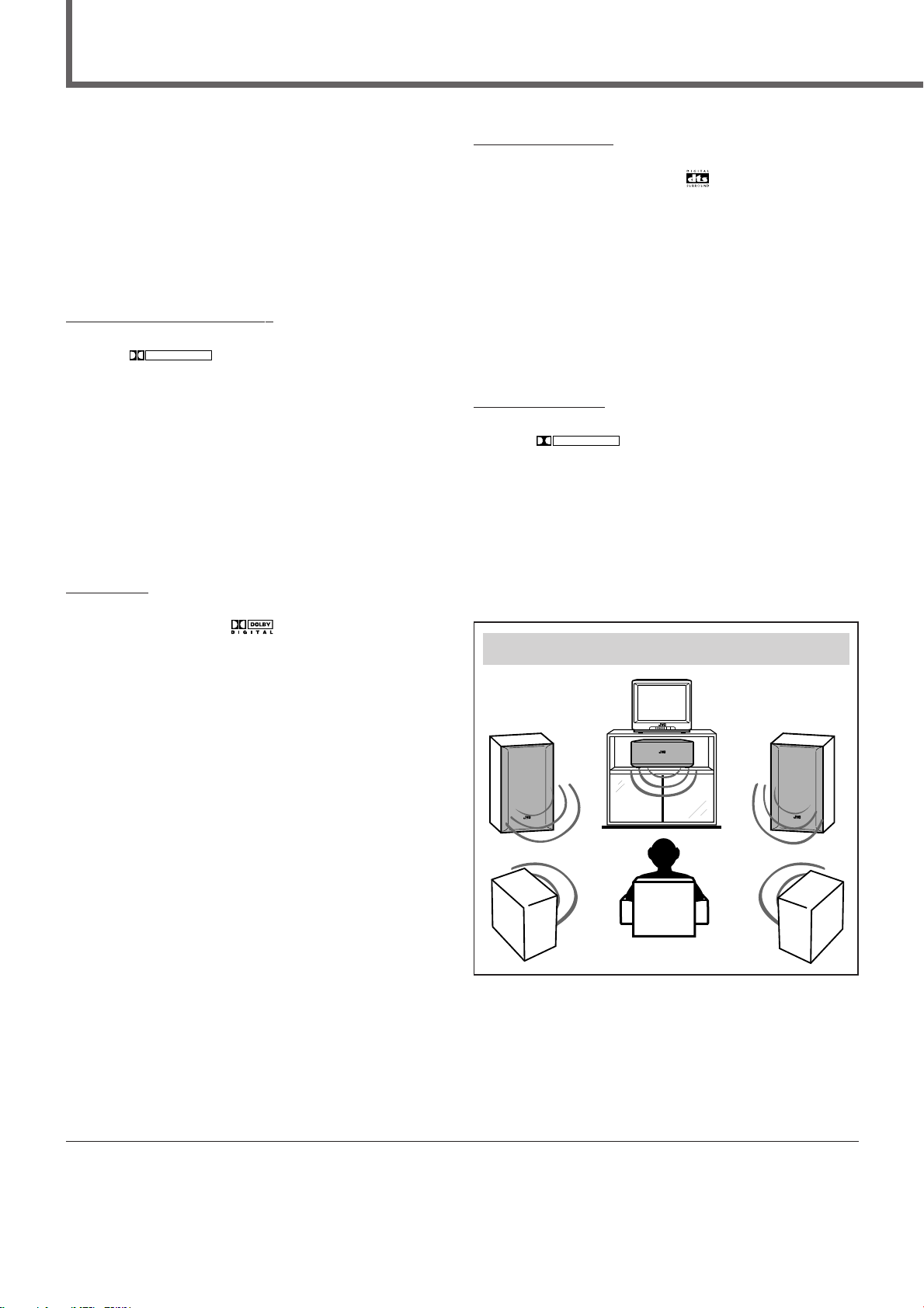
Creating Realistic Sound Fields
DOLBY SURROUND
You can use the following DSP (Digital Signal Processor) modes to
reproduce a realistic sound field.
• Surround modes
• DAP modes
■ Surround modes
Surround modes cannot be used when only the front speakers
are connected to this receiver (without the rear speakers or
center speaker).
Dolby Surround (Dolby Pro Logic)*
Used to reproduce sound tracks of the software encoded with Dolby
Surround (
Dolby Surround encoding format records the left front channel,
right front channel, center channel, and rear channel signals (total 4
channels) into 2 channels.
The Dolby Pro Logic decoder built in this receiver decodes these 2
channel signals into original 4 channel signals — matrix-based
multichannel reproduction, and allows you to enjoy a realistic stereo
sound in your listening room.
• When Dolby Pro Logic is activated, the PRO LOGIC indicator
lights up on the display.
– Dolby Pro Logic will be activated for all 2 channel-encoded
software.
DOLBY SURROUND
).
Dolby Digital*
Used to reproduce multichannel sound tracks of the software
encoded with Dolby Digital (
• To enjoy the software encoded with Dolby Digital, connect the
source component using the digital terminal on the rear of this
receiver. (See page 6.)
Dolby Digital encoding method (so-called discrete 5.1 channel
digital audio format) records and digitally compresses the left front
channel, right front channel, center channel, left rear channel, right
rear channel, and LFE channel signals (total 6 channels, but LFE
channel is counted as 0.1 channel. Therefore, called 5.1 channel).
Since each channel is completely independent from the other
channel signals to avoid interference, you can obtain much better
sound quality with much stereo and surround effects.
In addition, Dolby Digital enables stereo rear sounds, and sets the
cutoff frequency of the rear treble at 20 kHz, compared to 7 kHz for
Dolby Pro Logic. These facts enhance the sound movement and
being-there feelings much more than Dolby Pro Logic.
).
DTS Digital Surround**
Used to reproduce multichannel sound tracks of the software
encoded with DTS Digital Surround (
• To enjoy the software encoded with DTS Digital Surround,
connect the source component using the digital terminal on the
rear of this receiver. (See page 6.)
DTS Digital Surround is another discrete 5.1 channel digital audio
format available on CD, LD, and DVD software.
Compared to Dolby Digital, audio compression rate is relatively low.
This fact allows DTS Digital Surround format to add breadth and
depth to the reproduced sounds. As a result, DTS Digital Surround
features natural, solid and clear sound.
).
JVC Theater Surround
Used to reproduce sound tracks of the software encoded with Dolby
Surround (
• Theater Surround cannot be used only when the front
speakers and rear speakers are connected to this receiver
(without respect to the center speaker connection).
Theater Surround can add acoustic surround effects (DAP mode
effects) to Dolby Surround software, and create a sound field of a
theater in your listening room.
• When Theater Surround is selected, the PRO LOGIC and DSP
indicators light up on the display.
).
Surround reproduction
*
22
Manufactured under license from Dolby Laboratories. “Dolby,” “Pro
Logic,” and the double-D symbol are trademarks of Dolby
Laboratories. Confidential Unpublished Works. ©1992–1997 Dolby
Laboratories, Inc. All rights reserved.
**
Manufactured under license from Digital Theater Systems, Inc. US
Pat. No. 5,451,942 and other world-wide patents issued and
pending. “DTS” and “DTS Digital Surround” are trademarks of
Digital Theater Systems, Inc. ©1996 Digital Theater Systems, Inc.
All rights reserved.
Page 71

■ DAP (Digital Acoustic Processor) Modes
DAP modes have been designed to create important acoustic
surround elements.
The sound heard in a hall, live club, dance club or pavilion consists
of direct sound and indirect sound — early reflections and
reflections from behind. Direct sounds reach the listener directly
without any reflection. On the other hand, indirect sounds are
delayed by the distances of the ceiling and walls (see the diagram to
the right).
These indirect sounds are important elements of the acoustic
surround effects.
The following DAP modes are provided with this receiver.
These DAP modes can be used to add the acoustic surround effects
while reproducing stereo analog software or Linear PCM digital
software, and can give you a real “being there” feeling.
• DAP modes can be used when the front and rear speakers are
connected to this receiver (without respect to the center
speaker connection: no sound comes out of the center speaker
if it is connected).
• When one of the DAP modes is selected, the DSP indicator lights
up on the display.
Creating sound field
Creating Realistic Sound Fields
LIVE CLUB : Gives the feeling of a live music club with a low
ceiling.
DANCE CLUB : Gives a throbbing bass beat.
HALL : Gives clear vocal and the feeling of a concert
hall.
PAVILION : Gives the spacious feeling of a pavilion with a
high ceiling.
Available DSP modes according to the input signal format
Reflections from behind
Early reflections
Direct sounds
䡬: Possible ⳯: Impossible
DSP Modes SURROUND THEATER LIVE CLUB DANCE CLUB HALL PAVILION STEREO
Analog
Linear PCM
Dolby Digital
Input Signal format
*1Dolby Digital is activated except when 2 channel signals come in (in this case, Dolby Pro Logic is activated).
*2DTS Digital Surround is activated except when 2 channel signals come in (in this case, Dolby Pro Logic is activated).
DTS
(DTS Digital Surround)
䡬
(Dolby Pro Logic)
䡬
(Dolby Pro Logic)
1
䡬 *
(Dolby Digital)
2
䡬 *
䡬 䡬 䡬 䡬䡬䡬
䡬 䡬 䡬 䡬䡬䡬
⳯⳯⳯⳯⳯䡬
⳯⳯⳯⳯⳯䡬
23
Page 72

Creating Realistic Sound Fields
About Relations between Speaker Layout and DSP Modes
Available DSP modes will vary depending on how many speakers are used with this receiver.
Make sure that you have set the speaker information correctly (see page 12).
• If only front speakers are connected, you cannot use the DSP modes.
• If rear speakers are not connected, you cannot use Theater Surround and DAP modes.
5 Channels
Front
speaker
Rear
speaker
4 Channels
Front
speaker
Rear
speaker
Speaker Layouts
TV
Center speaker
TV
Front
speaker
Rear
speaker
Front
speaker
Rear
speaker
Available DSP modes
Surround mode
Each time you press SURROUND or SURROUND ON/OFF, Surround mode
turns on or off (“STEREO”):
SURROUND
DSP MODE
DOLBY D
LCR
SUBWFR LFE
LS RS
DGTL AUTO
VOL
(Remote)
SURROUND
ON/OFF
(Dolby Digital)
(Front panel)
DSP mode
Each time you press DSP MODE, the DSP modes (Theater Surround and DAP
modes) change as follows:
DSP MODE
(Remote)
DSP
MODE
(Front panel)
ANALOG
(back to the begining)
LR
SUBWFR
PRO LOGIC
DSP
VOL
3 Channels
Surround mode
Each time you press SURROUND or SURROUND ON/OFF, Surround mode
Front
speaker
TV
Center speaker
Front
speaker
turns on or off (“STEREO”):
SURROUND
DSP MODE
DOLBY D
LCR
SUBWFR LFE
LS RS
DGTL AUTO
(Remote)
SURROUND
ON/OFF
(Dolby Digital)
(Front panel)
When “AUTO SR (Auto Surround)” is turned “ON”
Surround mode is automatically activated when you select and start playing back a multichannel digital source.
VOL
24
Page 73

It will be convenient for you to use the remote control
for DSP operations, since you can adjust them from
your listening point, and use the test signal.
• When using the buttons on the front panel, see pages 29
to 31.
POWER
TV
TEST
SURROUND
SOUND
DVD
SURROUND
DSP MODE
SOUND
DVD
TV/VIDEO
+
TV VOL
–
+
+
TV/VCR
CH
–
HOME THEATER RECEIVER
VCR
– SUBWOOFER +TESTSLEEP
1
EFFECT
– CENTER +
4
5
5
BASS
– REAR•L +
BOOST
7
– REAR•R +
010
TV
VCR
FM
CD
+
VOLUME
–
£
1
7
RM-SRXE100J
REMOTE CONTROL
5
5
AUDIO
32
6
98
MENU
+10
ENTER
INPUT A/D
AM
MUTING
8
5
1
CENTER
+/–
REAR•L
+/–
REAR•R
+/–
Before you start, remember...
• Make sure that you have set the speaker information correctly
(see page 12).
• You cannot adjust the center speaker output level when you have
set “CTR SP” to “NO.”
• You cannot adjust the rear speaker output levels when you have set
“REAR SP” to “NO.”
• Remember not to change the speaker setting while using any DSP
mode; otherwise, it may be canceled when you deactivate the
speakers required for the DSP mode.
Using Surround Modes (Remote Control)
Surround mode cannot be used with another DSP mode. Once
Surround mode is activated, the other DSP mode in use will be
canceled.
• You have to make this adjustment for each source.
1
Select and play software encoded with Dolby
Surround, Dolby Digital, or DTS Digital
Surround.
If “AUTO SR (Auto Surround)” is set to “ON”
Playing a digital source automatically activates an appropriate
Surround mode. (See page 16.)
2
Press SURROUND to activate an appropriate
Surround mode — Pro Logic, Dolby Digital, or
DTS Digital Surround.
• Each time you press the button, Surround mode turns on and
off alternately.
SURROUND
DSP MODE
UTO
VOL
Then
Creating Realistic Sound Fields
IMPORTANT
To view the pictures on the TV, connect the video
components directly to the TV, and select an
appropriate input on the TV.
UTO
Ex.: When Dolby Digital is activated
Note:
When playing back an analog source, “SURROUND ON” will not
appear, and “PRO LOGIC” appears as soon as you press
SURROUND. (The PRO LOGIC indicator also lights up on the
display.)
3
Press SOUND.
SOUND
The 10 keys now work for sound adjustments.
TO BE CONTINUED ON THE NEXT PAGE
VOL
25
Page 74

Creating Realistic Sound Fields
4
Press TEST to check the speaker output balance.
TEST
1
LOGIC
L AUTO
T ATT
“TEST L” starts flashing on the display, and a test tone comes
out of the speakers in the following order:
(Left front speaker)
(Center speaker)
(Left rear speaker)
Notes:
• You can adjust the speaker output levels without outputting the
test tone.
• No test tone comes out of the center speaker when “CTR SP”
is set to “NO.”
• No test tone comes out of the rear speakers when “REAR SP”
is set to “NO.”
5
Adjust the following speaker output levels
(Right front speaker)
(Right rear speaker)
(from –10 to +10).
• Make adjustments so that the sound level of the selected
speaker is set at the same level as that of the front speakers.
To adjust the center speaker level, press CENTER +/–.
– CENTER +
5
6
LCR
SUBWFR LFE
LS S RS
98
LCR
MENU
SUBWFR LFE
LS S RS
PRO LOGIC
5
DSP
DGTL AUTO
INPUT ATT
PRO LOGIC
DSP
DGTL AUTO
INPUT ATT
ANALOG
LPCM
DOLBY D
DTS
To adjust the left rear speaker level, press REAR•L +/–.
– REAR•L +
ANALOG
5
LPCM
DOLBY D
DTS
To cancel Surround Mode
Press SURROUND again so that “STEREO” appears on the display.
• If Surround mode is canceled while playing back multichannel
VOL
VOL
VOL
digital software, all channel signals are mixed and output through
the front speakers (and subwoofer if you have connected a
subwoofer and set the subwoofer setting correctly – “YES.”)
TEST
EFFECT
DSP MODE
SOUND
POWER
TV
DVD
SURROUND
DSP MODE
SOUND
DVD
TV/VIDEO
+
TV VOL
–
+
+
TV/VCR
CH
–
HOME THEATER RECEIVER
VCR
– SUBWOOFER +TESTSLEEP
1
EFFECT
– CENTER +
4
5
5
BASS
– REAR•L +
BOOST
7
– REAR•R +
010
TV
VCR
FM
CD
+
VOLUME
–
£
1
7
RM-SRXE100J
REMOTE CONTROL
5
5
AUDIO
32
6
+10
ENTER
INPUT A/D
AM
MUTING
98
MENU
8
5
1
CENTER
+/–
REAR•L
+/–
REAR•R
+/–
To adjust the right rear speaker level, press REAR•R +/–.
– REAR•R +
ANALOG
0
LPCM
DOLBY D
DTS
6
Press TEST again to stop the test tone.
TEST
LCR
+10
SUBWFR LFE
LS S RS
1
ENTER
PRO LOGIC
DSP
DGTL AUTO
INPUT ATT
IC
TO
T
26
VOL
Using Theater Surround (Remote Control)
Theater Surround cannot be used with another DSP mode. Once
Theater Surround is activated, the other DSP mode in use will be
canceled.
• You have to make this adjustment for each source.
• You cannot use Theater Surround if no rear speakers are
connected.
VOL
1
Select and play software encoded with Dolby
Surround.
Page 75

2
T
VOL
Press DSP MODE repeatedly until “THEATER”
appears on the display.
The PRO LOGIC and DSP indicator light up on the display.
6
Press TEST again to stop the test tone.
TEST
1
Creating Realistic Sound Fields
DSP MODE
3
Press SOUND.
SOUND
4
Press TEST to check the speaker output balance.
TEST
1
ANALOG
The 10 keys now work for sound adjustments.
LOGIC
L AUTO
UT ATT
LR
SUBWFR
PRO LOGIC
DSP
“TEST L” starts flashing on the display, and a test tone comes
out of the speakers in the following order:
(Left front speaker)
(Center speaker)
(Left rear speaker)
Notes:
• You can adjust the speaker output levels without outputting the
test tone.
• No test tone comes out of the center speaker when “CTR SP”
is set to “NO.”
(Right front speaker)
(Right rear speaker)
7
Press EFFECT to select the DSP effect level (1 to
5) you want.
• As the number increases, the DSP effect becomes stronger
(normally set it to “EFFECT 3”).
EFFECT
4
5
LR
SUBWFR
LS S RS
PRO LOGIC
DSP
VOL
ANALOG
VOL
To cancel Theater Surround
Press DSP MODE repeatedly until “STEREO” appears on the
display. The PRO LOGIC and DSP indicators go off.
5
Adjust the following speaker output levels
(from –10 to +10).
• Make adjustments so that the sound level of the selected
speaker is set at the same level as that of the front speakers.
To adjust the center speaker level, press CENTER +/–.
– CENTER +
ANALOG
5
LPCM
DOLBY D
DTS
To adjust the left rear speaker level, press REAR•L +/–.
– REAR•L +
ANALOG
5
LPCM
DOLBY D
DTS
To adjust the right rear speaker level, press REAR•R +/–.
– REAR•R +
0
ANALOG
LPCM
DOLBY D
DTS
LCR
6
SUBWFR LFE
LS S RS
LCR
98
MENU
SUBWFR LFE
LS S RS
+10
LCR
ENTER
SUBWFR LFE
LS S RS
5
PRO LOGIC
DSP
DGTL AUTO
INPUT ATT
PRO LOGIC
DSP
DGTL AUTO
INPUT ATT
PRO LOGIC
DSP
DGTL AUTO
INPUT ATT
VOL
VOL
VOL
27
Page 76

ANALOG
PRO LOGIC
SUBWFR
VOL
DSP
LR
LS S RS
Creating Realistic Sound Fields
ANALOG
PRO LOGIC
SUBWFR LFE
VOL
DGTL AUTO
INPUT ATT
DSP
LCR
LS S RS
LPCM
DOLBY D
DTS
98
– REAR•L +
5
MENU
3
Press SOUND.
SOUND
The 10 keys now work for sound adjustments.
EFFECT
DSP MODE
SOUND
POWER
TV
DVD
SURROUND
DSP MODE
SOUND
DVD
TV/VIDEO
+
TV VOL
–
+
+
TV/VCR
CH
–
HOME THEATER RECEIVER
VCR
– SUBWOOFER +TESTSLEEP
1
EFFECT
– CENTER +
5
4
5
BASS
– REAR•L +
BOOST
7
– REAR•R +
010
TV
VCR
FM
CD
+
VOLUME
–
£
1
7
RM-SRXE100J
REMOTE CONTROL
5
5
AUDIO
32
6
98
MENU
+10
ENTER
INPUT A/D
AM
MUTING
8
4
Adjust the rear speaker output levels
(from –10 to +10).
• Make adjustments so that the sound level of the selected
REAR•L
5
+/–
speaker is set at the same level as that of the front speakers.
To adjust the left rear speaker level, press REAR•L +/–.
REAR•R
+/–
To adjust the right rear speaker level, press REAR•R +/–.
1
5
– REAR•R +
ANALOG
0
LPCM
DOLBY D
DTS
LCR
+10
SUBWFR LFE
ENTER
LS S RS
PRO LOGIC
DSP
DGTL AUTO
INPUT ATT
VOL
Press EFFECT to select the DSP effect level (1 to
5) you want.
• As the number increases, the DSP effect becomes stronger
(normally set it to “EFFECT 3”).
EFFECT
4
5
Using DAP Modes (Remote Control)
A DAP mode cannot be used with another DSP mode. Once one of
the DAP modes is activated, the other DSP mode in use will be
canceled.
• You have to make this adjustment for each source.
• You cannot use any DAP mode if no rear speakers are connected.
1
Select and play stereo analog software or Linear
PCM digital software.
2
Press DSP MODE repeatedly until one of the
DAP modes appears on the display.
The DSP indicator lights up on the display.
DSP MODE
ANALOG
LR
DSP
SUBWFR
28
LS S RS
(back to the begining)
VOL
To cancel DAP Mode
Press DSP MODE repeatedly so that “STEREO” appears on the
display. The DSP indicator goes off.
Page 77

CONTROL
5/∞/3/2
Creating Realistic Sound Fields
Display
POWER
STANDBY
DIGITAL
SURROUND
TV DILECT
SETTING
DIGITAL
ADJUST
CONTROL
ANALOG
LCR
LPCM
SUBWFR LFE
DOLBY D
LS S RS
MEMORY
DTS
DVD
DVD TV VCR CD FM
RX-E100
PRO LOGIC
SLEEP STTUNED MUTING
DSP
DGTL AUTO
INPUT ATT
ADJUST
IMPORTANT
To view the pictures on the TV, connect the video
components directly to the TV, and select an appropriate
input on the TV.
Before you start, remember...
• Make sure that you have set the speaker information correctly
(see page 12).
• You cannot adjust the center speaker output level when you have
set “CTR SP” to “NO.”
• You cannot adjust the rear speaker output levels when you have set
“REAR SP” to “NO.”
HOME THEATER RECEIVER
AUTO
MH
Z
KH
Z
VOL
AM
INPUT
ANALOG/DIGITAL
INPUT ATT
SURROUND
ON/OFF
DSP
MODE
MASTER V OLUME
SURROUND
ON/OFF
When using the remote control for DSP operations,
see pages 25 to 28.
2
Press SURROUND ON/OFF to activate an
appropriate Surround mode — Pro Logic, Dolby
Digital, or DTS Digital Surround.
• Each time you press the button, Surround mode turns on and
off alternately.
SURROUND
ON/OFF
UTO
VOL
Using Surround Modes (Front Panel)
Surround mode cannot be used with another DSP mode. Once
Surround mode is activated, the other DSP mode in use will be
canceled.
When using the buttons on the front panel, no test tone is available.
Make adjustments while listening to the sound of the source played
back.
• You have to make this adjustment for each source.
1
Select and play software encoded with Dolby
Surround, Dolby Digital, or DTS Digital
Surround.
If “AUTO SR (Auto Surround)” is set to “ON”
Playing a digital source automatically activates an appropriate
Surround mode. (See page 16.)
Then
UTO
Note:
Ex.: When Dolby Digital is activated
When playing back an analog source, “SURROUND ON” will not
appear, and “PRO LOGIC” appears as soon as you press
SURROUND. (The PRO LOGIC indicator also lights up on the
display.)
3
Press ADJUST .
ADJUST
The CONTROL buttons now work for sound
adjustments.
4
Press CONTROL ∞ (or 5) repeatedly until one
of the following indications (with the current
ANALOG
LPCM
DOLBY D
DTS
CONTROL
LCR
SUBWFR LFE
LS S RS
* appears.
PRO LOGIC
DSP
DGTL AUTO
INPUT ATT
setting)
VOL
VOL
TO BE CONTINUED ON THE NEXT PAGE
29
Page 78

Creating Realistic Sound Fields
DSP
MODE
ANALOG
PRO LOGIC
SUBWFR LFE
VOL
DGTL AUTO
INPUT ATT
DSP
LCR
LS S RS
LPCM
DOLBY D
DTS
ANALOG
PRO LOGIC
SUBWFR
DSP
LR
CONTROL
5/∞/3/2
Display
STANDBY
POWER
DIGITAL
SURROUND
TV DILECT
SETTING
DIGITAL
ADJUST
CONTROL
MEMORY
ADJUST
CENTER :To adjust the center speaker output level
(from –10 to +10).
REAR L : To adjust the left rear speaker output level
(from –10 to +10).
REAR R : To adjust the right rear speaker output level
(from –10 to +10).
* “0” is the initial setting for these speaker output levels.
If you have already changed the setting, another setting will be
shown.
5
Press CONTROL 3 (or 2) to adjust the speaker
output level.
• Make adjustments so that the sound level of the selected
speaker is set at the same level as that of the front speakers.
CONTROL
LCR
SUBWFR LFE
LS S RS
PRO LOGIC
DSP
DGTL AUTO
INPUT ATT
ANALOG
LPCM
DOLBY D
DTS
HOME THEATER RECEIVER
RX-E100
PRO LOGIC
ANALOG
SLEEP STTUNED MUTING
LCR
DSP
LPCM
SUBWFR LFE
DGTL AUTO
DOLBY D
LS S RS
DTS
INPUT ATT
DVD
DVD TV VCR CD FM
Using Theater Surround (Front Panel)
Theater Surround cannot be used with another DSP mode. Once
Theater Surround is activated, the other DSP mode in use will be
canceled.
When using the buttons on the front panel, no test tone is available.
Make adjustments while listening to the sound of the source played
back.
• You have to make this adjustment for each source.
• You cannot use Theater Surround if no rear speakers are
connected.
1
Select and play software encoded with Dolby
Surround.
2
Press DSP MODE repeatedly until “THEATER”
appears on the display.
VOL
The PRO LOGIC and DSP indicators light up on the display.
AUTO
MH
Z
KH
Z
VOL
AM
INPUT
ANALOG/DIGITAL
INPUT ATT
SURROUND
ON/OFF
DSP
MODE
MASTER V OLUME
DSP
MODE
Ex.: When adjusting the center speaker output level
6
Repeat steps 4 and 5 to adjust the other speaker
levels.
To cancel Surround Mode
Press SURROUND ON/OFF again so that “STEREO” appears on
the display.
• If Surround mode is canceled while playing back multichannel
digital software, all channel signals are mixed and output through
the front speakers (and subwoofer if you have connected a
subwoofer and set the subwoofer setting correctly – “YES.”)
30
3
Press ADJUST .
ADJUST
The CONTROL buttons now work for sound
adjustments.
4
Press CONTROL ∞ (or 5) repeatedly until one
of the following indications (with the current
setting)
* appears.
CONTROL
Page 79

ANALOG
PRO LOGIC
SUBWFR LFE
VOL
DGTL AUTO
INPUT ATT
DSP
LCR
LS S RS
LPCM
DOLBY D
DTS
CENTER :To adjust the center speaker output level
ANALOG
PRO LOGIC
SUBWFR LFE
VOL
DGTL AUTO
INPUT ATT
DSP
LCR
LS S RS
LPCM
DOLBY D
DTS
(from –10 to +10).
REAR L : To adjust the left rear speaker output level
(from –10 to +10).
REAR R : To adjust the right rear speaker output level
(from –10 to +10).
EFFECT : To adjust the DSP effect level. As the number
increases, the effect becomes stronger (normally set
it to “EFFECT 3”).
* “0” is the initial setting for the speaker output levels, and
“EFFECT 3” is for the DSP effect level.
If you have already changed the setting, another setting will be
shown.
5
Press CONTROL 3 (or 2) to make an
adjustment.
• When adjusting the speaker output levels, make adjustments
so that the sound level of the selected speaker is set at the
same level as that of the front speakers.
CONTROL
LCR
SUBWFR LFE
LS S RS
PRO LOGIC
DSP
DGTL AUTO
INPUT ATT
ANALOG
LPCM
DOLBY D
DTS
3
Creating Realistic Sound Fields
Press ADJUST .
ADJUST
4
Press CONTROL ∞ (or 5) repeatedly until one
of the following indications (with the current
setting)
CONTROL
REAR L : To adjust the left rear speaker output level
REAR R : To adjust the right rear speaker output level
VOL
EFFECT : To adjust the DSP effect level. As the number
The CONTROL buttons now work for sound
adjustments.
* appears.
(from –10 to +10).
(from –10 to +10).
increases, the effect becomes stronger (normally set
it to “EFFECT 3”).
Ex.: When adjusting the center speaker output level
6
Repeat steps 4 and 5 to make other
adjustments.
To cancel Theater Surround
Press DSP MODE repeatedly until “STEREO” appears on the
display. The PRO LOGIC and DSP indicators go off.
Using DAP Modes (Front Panel)
A DAP mode cannot be used with another DSP mode. Once one of
the DAP modes is activated, the other DSP mode in use will be
canceled.
• You have to make this adjustment for each source.
• You cannot use any DAP mode if no rear speakers are connected.
1
Select and play stereo analog software or Linear
PCM digital software.
2
Press DSP MODE repeatedly until one of the
DAP modes appears on the display.
The DSP indicator lights up on the display.
DSP
MODE
ANALOG
LR
DSP
SUBWFR
LS S RS
VOL
* “0” is the initial setting for the speaker output levels, and
“EFFECT 3” is for the DSP effect level.
If you have already changed the setting, another setting will be
shown.
5
Press CONTROL 3 (or 2) to make an
adjustment.
• When adjusting the speaker output levels, make adjustments
so that the sound level of the selected speaker is set at the
same level as that of the front speakers.
CONTROL
Ex.: When adjusting the left rear speaker output level
6
Repeat steps 4 and 5 to make other
adjustments.
To cancel DAP Mode
Press DSP MODE repeatedly so that “STEREO” appears on the
display. The DSP indicator goes off.
(back to the begining)
31
Page 80

Mastering Remote Operations
You can use the remote control to operate not only this
receiver but also other JVC products.
• Refer also to the manuals supplied for the other products.
– This remote control can operate a VCR whose remote
control code is set to A code.
• To operate the other products, aim the remote control
directly at the remote sensor on the target product.
DVD
P
O
TV
W
E
VCR
TEST
12
–
SU
BW
–C
E
N
T
E
R
–R
6
E
A
8
R
·L
+
9
E
A
R
M
E
·R
N
+
U
+10
E
INPUT A/D
N
T
E
R
R
AUDIO
O
OF
E
R
+
3
+
TV/VCR
CH
TV VOL
TV/VIDEO
SOUND
DVD
VOLUME
CD
SURROUND
DSP
MODE
TV
10
SLEEP
EFFECT
45
BASS
BOOST
7
–R
0
VCR
FM
AM
MUTING
❏ Selecting the source — Source selecting
buttons (see also page 8)
DVD
DVD : Select the DVD player.
TV : Select the TV.
VCR : Select the VCR.
CD : Select the CD player.
FM : Select the FM band.
AM : Select the AM band.
These buttons also change the functions of the 10 keys, and
make them work to operate the target source components. (See
the next page.)
TV
CD
VCR
FM
AM
❏ Selecting analog or digital input
— INPUT A/D button (see also page 11)
INPUT A/D
Select either analog input or digital input for
the digital source.
HOME THEA TER RECEIVER
RM-SRXE100J
REMOTE CONTROL
❏ Turning on the Power — POWER buttons
POWER
DVD
DVD : Turn on or off a JVC DVD player.
TV : Turn on or off a JVC TV.
VCR :Turn on or off a JVC VCR.
AUDIO : Turn on or off this receiver.
TV
VCR
AUDIO
❏ Turning off the sound temporarily
— MUTING button (see also page 9)
MUTING
Turn on or off the sound output.
❏ Creating realistic sound fields — SURROUND
and DSP MODE buttons (see also pages 24 – 28)
SURROUND
DSP MODE
SURROUND : Turn on or off Surround
mode.
DSP MODE : Select the DSP modes
(Theater Surround and DAP
modes). Each time you press
the button, the DSP modes
change.
❏ Adjusting the sound — SOUND button
(see also pages 18, 19, 25, 27, 28)
SOUND
Change the functions of 10 keys, and make
them work for sound adjustments.
❏ Turning off the receiver automatically
— SLEEP button (see also page 9)
❏ Adjusting the volume — VOLUME buttons
(see also page 8)
+
VOLUME
Adjust the volume level.
–
32
SLEEP
Set the shut-off time until the receiver turns
off automatically.
Page 81
❏ Adjusting the sound and operating other JVC
products — 10 keys
❏ Operating other JVC products — Audio/video
operation buttons
Mastering Remote Operations
– SUBWOOFER +TEST
1
EFFECT
4
BASS
BOOST
7
5
– CENTER +
5
– REAR•L +
– REAR•R +
010
32
5
6
5
98
5
MENU
+10
ENTER
■ After pressing SOUND, you can use the 10 keys for sound
adjustments. (See also pages 18, 19, 25 – 28)
TEST :Turn on or off the test tone output.
EFFECT :Change the DSP effect level.
BASS BOOST : Turn on or off Bass Boost.
SUBWOOFER +/– : Adjust the subwoofer level.
CENTER +/– : Adjust the center speaker output
level.
REAR L +/– : Adjust the left rear speaker output
level.
REAR R +/– :Adjust the right rear speaker output
level.
■ After pressing DVD (source selecting button), you can use
the 10 keys (2, 4, 6, 8, 9, +10) for DVD menu operations.
MENU : Display the menu screen.
ENTER : Enter a selected item.
5 / ∞ / 2 / 3 : Select an item on the menu screen.
■ After pressing TV (source selecting button), you can use the
10 keys for selecting a channel on the TV.
1 – 9, 0 : Select a channel.
10 : Functions as the RETURN button.
+10 : Functions as the +100 button.
■ After pressing VCR (source selecting button), you can use
the 10 keys for VCR operations.
1 – 9, 0 :Select a channel on the VCR.
8
£
+
+
TV/VCR
CH
1
–
7
■ After pressing DVD (source selecting button), you can use
the following buttons for DVD operations.
3 : Start playback.
7 : Stop playback.
8 : Pause playback. To release it, press 3.
¢ : Skip to the beginning of the next track.
4 : Return to the beginning of the current
(or previous) track.
■ After pressing TV (source selecting button), you can use the
following buttons for changing the channels on the TV.
TV/VCR CH +/– :Change channel numbers.
■ After pressing VCR (source selecting button), you can use
the following buttons for VCR operations.
TV/VCR CH +/– : Change channel numbers on the VCR.
3 : Start playback.
7 : Stop playback.
8 : Pause playback. To release it, press 3.
¡ : Fast-wind a tape.
1 : Rewind a tape.
■ After pressing CD (source selecting button), you can use
the following buttons for CD operations.
3 : Start playback.
7 : Stop playback.
8 : Pause playback. To release it, press 3.
¢ : Skip to the beginning of the next track.
4 : Return to the beginning of the current
(or previous) track.
1
■ After pressing CD, you can use the 10 keys for CD
operations.
1 – 10, +10 : Select a track.
■ After pressing FM or AM, you can use the 10 keys for
tuner operations.
1 – 10, +10 : Select a preset channel.
Example: Selecting CD track numbers or preset FM/AM
channel numbers using the 10 keys
• For number 5, press 5.
• For number 15, press +10, then 5.
• For number 30, press +10, +10, then 10.
■ These buttons works only for TVs.
TV/VIDEO
TV/VIDEO : Change the input mode (Video
input and TV tuner) on the TV.
TV VOL +/– : Adjust the volume on the TV.
+
TV VOL
–
33
Page 82

Parts Identification
Front Panel
1
POWER
1
2
3
4
5
6
7
8
9
STANDBY
2
TV DILECT
ANALOG
CONTROL
ADJUST
SETTING
DIGITAL
DIGITAL
SURROUND
4 5 7 9 p q
MEMORY
6
Remote Control
LCR
LPCM
SUBWFR LFE
DOLBY D
LS S RS
DTS
DVD
DVD TV VCR CD FM
3
HOME THEATER RECEIVER
RX-E100
PRO LOGIC
SLEEP STTUNED MUTING
DSP
DGTL AUTO
INPUT ATT
8
See pages in the parentheses for details.
AUTO
MH
Z
KHZ
VOL
ANALOG/DIGITAL
INPUT ATT
AM
Front Panel
1 POWER button and STANDBY lamp (8)
2 Remote sensor
3 Display
4 SETTING button (10, 12 – 16)
5 ADJUST button (17 – 19, 29 – 31)
POWER
TV
DVD
SURROUND
DSP MODE
SOUND
DVD
TV/VIDEO
+
TV VOL
–
+
+
TV/VCR
CH
–
HOME THEATER RECEIVER
VCR
– SUBWOOFER +TESTSLEEP
1
EFFECT
– CENTER +
54
5
BASS
– REAR•L +
BOOST
7
– REAR•R +
010
TV
VCR
FM
CD
+
VOLUME
–
£
1
7
RM-SRXE100J
REMOTE CONTROL
5
5
AUDIO
32
6
98
MENU
+10
ENTER
INPUT A/D
AM
MUTING
8
5
p
q
w
e
1
r
6 CONTROL buttons (10 – 21, 29 – 31)
5 / ∞ / 2 / 3
7 MEMORY button (20, 21)
8 Source selecting buttons (8, 11, 20, 21)
DVD, TV, VCR, CD, FM, AM
9 INPUT ANALOG/DIGITAL button (11)
INPUT ATT button (17)
p SURROUND ON/OFF button (24, 29)
q DSP MODE button (24, 30, 31)
w VOLUME
/ buttons (8)
Remote Control
1 POWER buttons (8, 32)
TV, VCR, AUDIO
2 SLEEP button (9, 32)
3 SURROUND button (24, 25, 32)
4 DSP MODE button (24, 27, 28, 32)
5 SOUND button (18, 19, 25, 27, 28, 32)
6 Source selecting buttons (8, 11, 20, 21)
DVD, TV, VCR, CD, FM, AM
7 TV/VIDEO button (33)
8 TV VOL +/– buttons (33)
9 TV/VCR CH +/– buttons (33)
p • 10 keys for selecting preset channels (21, 33)
• 10 keys for adjusting sound (18, 19, 26 – 28)
• 10 keys for operating audio/video components (33)
q INPUT A/D (analog/digital) button (11)
w MUTING button (9)
e VOLUME +/– buttons (8)
r Operating buttons for audio/video components (33)
SURROUND
ON/OFF
DSP
MODE
MASTER VOLUME
INPUT
w
34
Page 83

Troubleshooting
Use this chart to help you solve daily operational problems. If there is any problem you cannot solve, contact your JVC service center.
PROBLEM
The power does not comes on.
No sound from speakers.
Sound from one speaker only.
Continuous hiss or buzzing during FM
reception.
The power cord is not plugged in.
Speaker signal cables are not
connected.
An incorrect source is selected.
Muting is activated.
An incorrect input mode (analog or
digital) is selected.
Connections are incorrect.
The balance is set to one extreme.
Incoming signal is too weak.
The station is too far away.
An incorrect antenna is used.
POSSIBLE CAUSE
SOLUTION
Plug the power cord into an AC outlet.
Check speaker wiring and reconnect if
necessary.
Select the correct source.
Press MUTING to cancel the mute.
Select the correct input mode (analog or
digital).
Check connections.
Adjust the balance properly (see page 17).
Connect an outdoor FM antenna or contact
your dealer.
Select a new station.
Check with your dealer to be sure you have
a correct antenna.
Parts Identification/Troubleshooting
Occasional cracking noise during FM
reception.
“OVERLOAD” starts flashing on the
display.
The STANDBY lamp lights up after
turning on the power, but soon the
receiver turns off (into standby mode).
Remote control does not operate as you
intend.
Antennas are not connected properly.
Ignition noise from automobiles.
Speakers are overloaded because of
high volume.
Speakers are overloaded because of
short circuit of speaker terminals.
The receiver is overloaded because of a
high voltage.
The remote control is not ready for
your intended operation.
Check connections.
Move the antenna farther from automobile
traffic.
1. Press POWER on the front panel to turn
off the receiver.
2. Stop the playback source.
3. Turn on the receiver again, and adjust
the volume.
Press POWER on the front panel to turn off
the receiver, then check the speaker wiring.
If “OVERLOAD” does not disappear,
unplug the AC power cord, then plug it
back again.
If speaker wiring is not short-circuited,
contact your dealer.
Press POWER on the front panel to turn off
the receiver. After unplugging the power
cord, consult your dealer.
Press SOUND or source selecting buttons
first, then press the button you want to use.
(See pages 32 and 33.)
Remote control does not work.
There is an obstruction hiding the
remote sensor on the receiver.
Batteries are weak.
Remove the obstruction.
Replace batteries.
35
Page 84

Specifications
Amplifier
Designs & specifications are subject to change without notice.
Output Power At Stereo operation:
Front channels:
70 W per channel, min. RMS, driv en into 8 Ω,
40 Hz to 20 kHz with no more than 0.8% total
harmonic distortion.
At Surround operation:
Front channels: 70 W per channel, min. RMS, driven into 8 Ω at 1 kHz with no
more than 0.8% total harmonic distortion.
Center channel: 70 W, min. RMS, driven into 8 Ω at 1 kHz, with no more than
0.8% total harmonic distortion.
Rear channels: 70 W per channel, min. RMS, driven into 8 Ω at 1 kHz, with no
more than 0.8% total harmonic distortion.
Audio Input Sensitivity/Impedance (1 kHz): CD, TV, VCR, DVD: 200 mV/47 k Ω
Audio Input (DIGITAL IN)* : Coaxial: DIGITAL 1 (DVD): 0.5 V p-p/75 Ω
Optical: DIGITAL 2 (TV): –21 dBm to –15 dBm (660 nm ±30 nm)
*Corresponding to Linear PCM, Dolby Digital, and DTS Digital Surround
(with sampling frequency — 32 kHz, 44.1 kHz, 48 kHz).
Audio Output Level: VCR: 200 mV
Signal-to-Noise Ratio (’66 IHF/’78 IHF): CD, TV, VCR, DVD: 85 dB/75 dB
Frequency Response (8 Ω): CD, TV, VCR, DVD: 20 Hz to 20 kHz (±1 dB)
Tone Control: Bass (100 Hz): ±10 dB
Treble (10 kHz): ±10 dB
Bass Boost: +6 dB ± 1 dB at 70 Hz
FM tuner (IHF)
Tuning Range: 87.5 MHz to 108.0 MHz
Usable Sensitivity: Monaural: 12.8 dBf (1.2 µV/75 Ω)
50 dB Quieting Sensitivity: Monaural: 21.3 dBf (3.2 µV/75 Ω)
Stereo: 41.3 dBf (31.5 µV/75 Ω)
Signal-to-Noise Ratio (IHF-A weighted): Monaural: 78 dB at 85 dBf
Stereo: 73 dB at 85 dBf
Total Harmonic Distortion: Monaural: 0.4% at 1 kHz
Stereo: 0.6% at 1 kHz
Stereo Separation at REC OUT: 35 dB at 1 kHz
Alternate Channel Selectivity: 45 dB: (±400 kHz)
Frequency Response: 30 Hz to 15 kHz: (+0.5 dB, –3 dB)
AM tuner
Tuning Range: 530 kHz to 1 710 kHz
Usable Sensitivity: Loop antenna 400 µV/m
Signal-to-Noise Ratio: 50 dB (100 mV/m)
General
Power Requirements: AC 120V , 60 Hz
Power Consumption: 150 W/190 VA (at operation)
2 W (in standby mode)
Dimensions (W x H x D): 17 3/16 in. x 3 15/16 in. x 15 11/16 in.
(435 mm x 100 mm x 398 mm)
Mass: 16.4 lbs (7.4 kg)
36
Page 85

Memorandum
Note the adjustments you have made for each source below for your future reference.
The following adjustments can be stored for each source:
• Analog/digital input mode (see page 11)
• Input attenuator mode (see page 17)
• Balance (see page 17)
• Bass boost (see page 18)
Source Name:
•Analog/digital input: ANALOG / DGTL AUTO
•Input Attenuator: ON / NORMAL
•Bass Boost: ON / OFF
•Tone adjustment
Bass:
Treble:
•Subwoofer level
•Balance
•Surround mode/Theater Surround/DAP modes
Mode: SURROUND / THEATER
LIVE CLUB
DANCE CLUB / HALL
PAVILION / STEREO
• Tone adjustment (see page 19)
• Subwoofer level (see page 19)
• Surround mode settings (see pages 25, 29)
Theater Surround settings (see pages 27, 30)
DAP mode settings (see pages 28, 31)
Source Name:
•Analog/digital input: ANALOG / DGTL AUTO
•Input Attenuator: ON / NORMAL
•Bass Boost: ON / OFF
•Tone adjustment
Bass:
Treble:
•Subwoofer level
•Balance
•Surround mode/Theater Surround/DAP modes
Mode: SURROUND / THEATER
Specifications/Memorandum
LIVE CLUB
DANCE CLUB / HALL
PAVILION / STEREO
Center level :
Left rear level:
Right rear level :
Effect level:
• Analog/digital input: ANALOG / DGTL AUTO
•Input Attenuator: ON / NORMAL
•Bass Boost: ON / OFF
•Tone adjustment
Bass:
Treble:
•Subwoofer level
•Balance
•Surround mode/Theater Surround/DAP modes
Mode: SURROUND / THEATER
LIVE CLUB
DANCE CLUB / HALL
PAVILION / STEREO
Center level :
Left rear level:
Right rear level :
Effect level:
Center level :
Left rear level:
Right rear level :
Effect level:
37
Page 86

QUALITY SERVICE
HOW TO LOCATE YOUR JVC SERVICE CENTER
TOLL FREE : 1-800-537-5722
http://www.jvcservice.com
Dear customer:
In order to receive the most satisfaction from your purchase, read the instruction booklet before operating the unit. In the event that repair
is necessary, or for the address nearest your location, please refer to the factory service center list below or within the Continental
United States, Call 1-800-537-5722 for your authorized servicer. Remember to retain your Bill of Sale for Warranty Service.
—JVC
JVC SERVICE & ENGINEERING
COMPANY OF AMERICA
DIVISION OF JVC AMERICAS CORP.
FACTORY SERVICE CENTER LOCATIONS
10 New Maple Avenue
Pine Brook, NJ 07058-9641
(973) 396-1000
5665 Corporate Avenue
Cypress, CA 90630-0024
(714) 229-8011
13 Cummings Park
Woburn, MA 01801
(781) 376-9100
Sophisticated electronic products may require occasional service. Just as quality is a keyword in the engineering and production of
the wide array of JVC products, service is the key to maintaining the high level of performance for which JVC is world famous. The
JVC service and engineering organization stands behind our products.
1500 Lakes Parkway
Lawrenceville, GA 30243-5857
(770) 339-2582
2969 Mapunapuna Place
Honolulu, HI 96819-2040
(808) 833-5828
8192 State Road 84
Davie, FL 33324
(954) 472-1960
NATIONAL HEADQUARTERS
JVC SERVICE & ENGINEERING COMPANY OF AMERICA
DIVISION OF JVC AMERICAS CORP.
1700 Valley Road
Wayne, NJ 07470
If you ship the product • • •
Pack your JVC unit in the original carton or one of equivalent
size and strength. Enclose, with the unit, a letter stating the
problem or symptom that exists and also a copy of the
receipt or bill of sale you received when you purchased your
JVC unit. Print your home return address on the outside
and the inside of the carton. Send to the appropriate JVC
Factory Service Center as listed above.
To prevent electrical shock, do not open the cabinet. No user
serviceable parts inside.
Refer servicing to qualified service personnel.
705 Enterprise Street
Aurora, IL 60504-8149
(630) 851-7855
10700 Hammerly, Suite 110
Houston, TX 77043
(713) 935-9331
890 Dubuque Avenue
South San Francisco, CA 94080-1804
(650) 871-2666
Don’t service it yourself.
CAUTION
(1099)
ACCESSORIES
To purchase accessories for your JVC product, you may contact your local JVC Dealer.
Or from the 48 Continental United States call toll free : 800-882-2345
Page 87

LIMITED W ARRANTY AUDIO-2
JVC COMPANY OF AMERICA warrants this product and all parts thereof, except as set forth below ONLY TO THE ORIGINAL
PURCHASER AT RETAIL to be FREE FROM DEFECTIVE MATERIAL AND WORKMANSHIP from the date of original retail
purchase for the period as shown below. (“The Warranty Period.”)
PARTS LABOR
THIS LIMITED WARRANTY IS VALID ONLY IN THE FIFTY(50) UNITED STATES, THE DISTRICT OF COLUMBIA AND IN
COMMONWEALTH OF PUERTO RICO.
WHAT WE WILL DO:
If this product is found to be defective, JVC will repair or replace defective parts at no charge to the original owner. Such
repair and replacement services shall be rendered by JVC during normal business hours at JVC authorized service centers.
Parts used for replacement are warranted only for the remainder of the Warranty Period. All products and parts thereof may be
brought to a JVC authorized service center on a carry-in basis except for Television sets having a screen size 25 inches and
above which are covered on an in-home basis.
WHAT YOU MUST DO FOR WARRANTY SERVICE:
Return your product to a JVC authorized service center with a copy of your bill of sale. For your nearest JVC authorized
service center, please call toll free: (800)537-5722.
If service is not available locally, box the product carefully, preferably in the original carton, and ship, insured, with a copy of
your bill of sale plus and letter of explanation of the problem to the nearest JVC Factory Service Center, the name and location
of which will be given to you by the toll-free number.
If you have any questions concer ning your JVC Product, please contact our Customer Relations Department.
WHAT IS NOT COVERED:
This limited warranty provided by JVC does not cover:
1. Products which have been subject to abuse, accident, alteration, modification, tampering, negligence, misuse, faulty
installation, lack of reasonable care, or if repaired or serviced by anyone other than a service facility authorized by JVC to
render such service, or if affixed to any attachment not provided with the products, or if the model number or serial number
has been altered, tampered with, defaced or removed;
2. Initial installation and installation and removal for repair;
3. Operational adjustments covered in the Owner’s Manual, normal maintenance, video and audio head cleaning;
4. Damage that occurs in shipment, due to act of God, and cosmetic damage;
2YR 2YR
5. Signal reception problems and failures due to line power surge;
6. Video Pick-up Tubes/CCD Image Sensor, Cartridge, Stylus(Needle) are covered for 90 days from the date of purchase;
7. Accessories;
8. Batteries (except the Rechargeable Batteries are covered for 90 days from the date of purchase);
There are no express warranties except as listed above.
THE DURATION OF ANY IMPLIED WARRANTIES, INCLUDING THE IMPLIED WARRANTY OF MERCHANTABILITY, IS
LIMITED TO THE DURATION OF THE EXPRESS WARRANTY HEREIN.
JVC SHALL NOT BE LIABLE FOR THE LOSS OF USE OF THE PRODUCT, INCONVENIENCE, LOSS OR ANY OTHER
DAMAGES, WHETHER DIRECT, INCIDENTAL OR CONSEQUENTIAL (INCLUDING, WITHOUT LIMITATION, DAMAGE TO
TAPES, RECORDS OR DISCS) RESULTING FROM THE USE OF THIS PRODUCT, OR ARISING OUT OF ANY BREACH OF
THIS WARRANTY. ALL EXPRESS AND IMPLIED WARRANTIES, INCLUDING THE WARRANTIES OF MERCHANTABILITY
AND FITNESS FOR PARTICULAR PURPOSE, ARE LIMITED TO THE WARRANTY PERIOD SET FORTH ABOVE.
Some states do not allow the exclusion of incidental or consequential damages or limitations on how long an implied
warranty last, so these limitations or exclusions may not apply to you. This warranty gives you specific legal rights and you may
also have other rights which vary from state to state.
JVC COMPANY OF AMERICA 1700 Valley Road
DIVISION OF JVC AMERICAS CORP. Wayne, NJ 07470
REFURBISHED PRODUCTS CARRY A SEPARATE WARRANTY, THIS WARRANTY DOES NOT APPLY. FOR DETAILS OF
REFURBISHED PRO DUCT WARRANTY, PLEASE REFER TO THE REFURBISHED PRODUCT WARRANTY INFORMATION
PACKAGED WITH EACH REFURBISHED PRODUCT.
For customer use:
Enter below the Model No. and Serial No. which is located either on the rear, bottom or side of the cabinet. Retain this
information for future reference.
Model No.: Serial No.:
Purchase date: Name of dealer:
Page 88

VICTOR COMPANY OF JAPAN, LIMITED
EN
0301NHMMDWJEIN
JVC
 Loading...