

Page 1
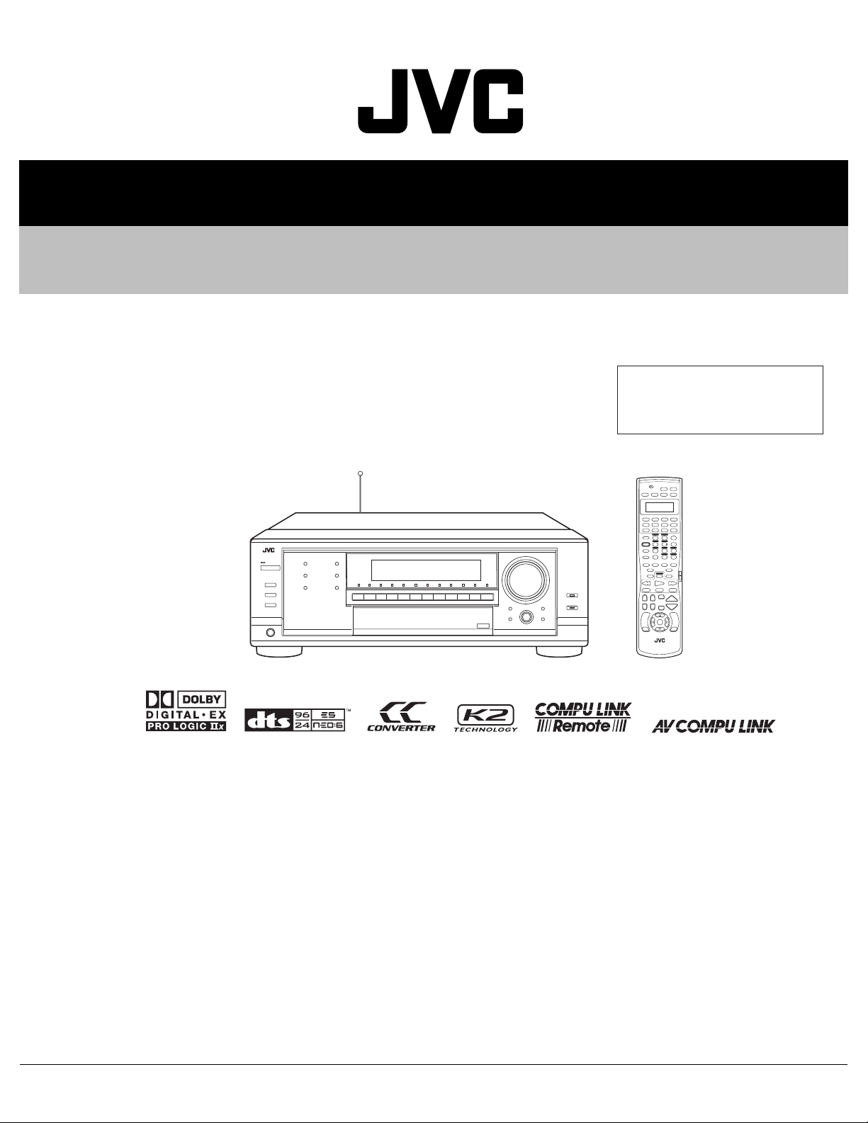
SERVICE MANUAL
AUDIO/VIDEO CONTROL RECEIVER
MB30320047
RX-8040B
Area suffix
UJ ---------------------- U.S.Military
TABLE OF CONTENTS
1 PRECAUTION. . . . . . . . . . . . . . . . . . . . . . . . . . . . . . . . . . . . . . . . . . . . . . . . . . . . . . . . . . . . . . . . . . . . . . . . . 1-3
2 SPECIFIC SERVICE INSTRUCTIONS . . . . . . . . . . . . . . . . . . . . . . . . . . . . . . . . . . . . . . . . . . . . . . . . . . . . . . 1-4
3 DISASSEMBLY . . . . . . . . . . . . . . . . . . . . . . . . . . . . . . . . . . . . . . . . . . . . . . . . . . . . . . . . . . . . . . . . . . . . . . . 1-5
4 ADJUSTMENT . . . . . . . . . . . . . . . . . . . . . . . . . . . . . . . . . . . . . . . . . . . . . . . . . . . . . . . . . . . . . . . . . . . . . . . 1-15
5 TROUBLESHOOTING . . . . . . . . . . . . . . . . . . . . . . . . . . . . . . . . . . . . . . . . . . . . . . . . . . . . . . . . . . . . . . . . . 1-16
COPYRIGHT © 2004 Victor Company of Japan, Limited
No.MB303
2004/7
Page 2
SPECIFICATION
Amplifier
Output Power At Stereo Operation Front Channel 100 W*1 per channel, min. RMS, driven into 8
harmonic distortion (IEC268-3/DIN).
At Surround Operation
Audio Audio Input Sensitivity/Impedance (1 kHz) DVD IN, VCR 1 IN, VCR 2 IN, TV SOUND/DBS IN, VIDEO:200 mV/47 k
Audio Input (DIGITAL IN)*2
Audio Output Level ZONE 2 PREOUT:1 V
Recording Output Level TAPE/MD OUT, CDR OUT, VCR 1 OUT, VCR 2 OUT:200 mV
Digital Output (DIGITAL OUT):Optical Signal wave length:660 nm
Signal-to-Noise Ratio ('66 IHF/'78 IHF) DVD IN, VCR 1 IN, VCR 2 IN, TV SOUND/DBS IN, VIDEO:87 dB/80 dB
Frequency Response (8
RIAA Phono Equalization ±1.0 dB (20 Hz to 20 kHz)
Bass Boost +6 dB ±1.0 dB at 100 Hz
Equalization 63 Hz, 250 Hz, 1 kHz, 4 kHz, 16 kHz: ±8 dB (in 2 dB steps)
Video Video Input Sensitivity/Impedance Composite Video:DVD IN, TV SOUND/
Video Output Level Composite Video:VCR 1 OUT, VCR 2
Synchronization Negative
Signal-to-Noise Ratio 45 dB
Tuning Range 87.50 MHz to 108.00 MHz
Usable Sensitivity Monaural 12.8 dBf (1.2
50 dB Quieting Sensitivity Monaural 16.0 dBf (1.7
Stereo Separation at OUT (REC) 35 dB at 1 kHz
Tuning Range 531 kHz to 1 602 kHz (at 9 kHz intervals)
Power Requirements AC 110 V/127 V/220 V/230 V - 240 V , adjustable with the voltage selector, 50 Hz/60 Hz
Power Consumption 220 W (at operation) 6.0 W (in standby mode)
Dimensions (W
Mass 12.4 kg
× H × D) 435 mm × 157 mm × 425 mm
Front Channel 100 W*1 per channel, min. RMS, driven into 8
harmonic distortion.
Center Channel 100 W*1, min. RMS, driven into 8
distortion.
Surround Channel 100 W*1 per channel, min. RMS, driven into 8
harmonic distortion.
Surround Back Channel 100 W*1, min. RMS, driven into 8
distortion.
TAPE/MD IN, CDR IN, CD IN:200 mV/47 kΩ
PHONO IN (MM):2.5 mV/47 kΩ
Coaxial DIGITAL 1 (DVD):0.5 V(p-p)/75 Ω
Optical DIGITAL 2 (CD), DIGITAL 3 (TV), DIGITAL 4 (CDR):-21 dBm to -15 dBm (660 nm ±30
nm)
PREOUT:1 V
Output level:-21 dBm to -15 dBm
TAPE/MD IN, CDR IN, CD IN:87 dB/80 dB
PHONO IN (MM):70 dB/78 dB at OUT (REC)
Ω at 1 kHz, with no more than 0.8% total harmonic
Ω at 1 kHz, with no more than 0.8% total harmonic
Ω) DVD IN, VCR 1 IN, VCR 2 IN, TV SOUND/DBS IN, VIDEO:20 Hz to 100 kHz (+1 dB, -
3 dB)
TAPE/MD IN, CDR IN, CD IN:20 Hz to 100 kHz (+1 dB, -3 dB)
PHONO IN (MM):20 Hz to 20 kHz (±1 dB)
DBS IN, VCR 1 IN, VCR 2 IN, VIDEO
S-video:DVD IN, TV SOUND/DBS IN, VCR
1 IN, VCR 2 IN, VIDEO
Component Video :DVD IN, DBS (VCR 1)
IN
OUT, MONITOR OUT
S-video:VCR 1 OUT, VCR 2 OUT, MONI-
TOR OUT
Composite Video:MONITOR OUT (Y: luminance):1 V(p-p)/75 Ω
FM tuner (IHF)
µV/75 Ω)
µV/75 Ω)
Stereo 37.5 dBf (20.5
530 kHz to 1 600 kHz (at 10 kHz intervals)
µV/75 Ω)
AM tuner
General
*1: Measured on AC 110 V, 127 V, 220 V and 240 V
*2: Corresponding to Linear PCM, Dolby Digital, and DTS (with sampling frequency -32 kHz, 44.1 kHz, 48 kHz).
Designs & specifications are subject to change without notice.
Ω at 1 kHz with no more than 0.8% total
Ω at 1 kHz, with no more than 0.8% total
Ω at 1 kHz, with no more than 0.8% total
Ω
1 V(p-p)/75
(Y: luminance):1 V(p-p)/75 Ω
(C: chrominance, burst):0.286 V(p-p)/75 Ω
(Y: luminance):1 V(p-p)/75 Ω
(PB/PR):0.7 V(p-p)/75 Ω
1 V(p-p)/75 Ω
(Y: luminance):1 V(p-p)/75 Ω
(C: chrominance, burst):0.286 V(p-p)/75 Ω
(PB/PR):0.7 V(p-p)/75 Ω
Ω
1-2 (No.MB303)
Page 3
SECTION 1
PRECAUTION
1.1 Safety Precautions
(1) This design of this product contains special hardware and
many circuits and components specially for safety purposes. For continued protection, no changes should be made
to the original design unless authorized in writing by the
manufacturer. Replacement parts must be identical to
those used in the original circuits. Services should be performed by qualified personnel only.
(2) Alterations of the design or circuitry of the product should
not be made. Any design alterations of the product should
not be made. Any design alterations or additions will void
the manufacturers warranty and will further relieve the
manufacture of responsibility for personal injury or property
damage resulting therefrom.
(3) Many electrical and mechanical parts in the products have
special safety-related characteristics. These characteristics are often not evident from visual inspection nor can the
protection afforded by them necessarily be obtained by using replacement components rated for higher voltage, wattage, etc. Replacement parts which have these special
safety characteristics are identified in the Parts List of Service Manual. Electrical components having such features
are identified by shading on the schematics and by ( ) on
the Parts List in the Service Manual. The use of a substitute
replacement which does not have the same safety characteristics as the recommended replacement parts shown in
the Parts List of Service Manual may create shock, fire, or
other hazards.
(4) The leads in the products are routed and dressed with ties,
clamps, tubings, barriers and the like to be separated from
live parts, high temperature parts, moving parts and/or
sharp edges for the prevention of electric shock and fire
hazard. When service is required, the original lead routing
and dress should be observed, and it should be confirmed
that they have been returned to normal, after reassembling.
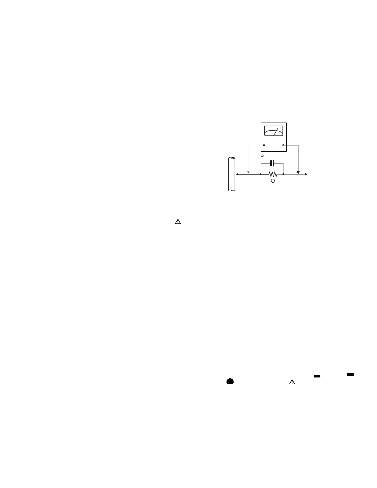
(5) Leakage shock hazard testing
After reassembling the product, always perform an isolation check on the exposed metal parts of the product (antenna terminals, knobs, metal cabinet, screw heads,
headphone jack, control shafts, etc.) to be sure the product
is safe to operate without danger of electrical shock.Do not
use a line isolation transformer during this check.
• Plug the AC line cord directly into the AC outlet. Using a
"Leakage Current Tester", measure the leakage current
from each exposed metal parts of the cabinet, particularly any exposed metal part having a return path to the
chassis, to a known good earth ground. Any leakage current must not exceed 0.5mA AC (r.m.s.).
• Alternate check method
Plug the AC line cord directly into the AC outlet. Use an
AC voltmeter having, 1,000Ω per volt or more sensitivity
in the following manner. Connect a 1,500Ω 10W resistor
paralleled by a 0.15µF AC-type capacitor between an ex-
posed metal part and a known good earth ground.
Measure the AC voltage across the resistor with the AC
voltmeter.
Move the resistor connection to each exposed metal
part, particularly any exposed metal part having a return
path to the chassis, and measure the AC voltage across
the resistor. Now, reverse the plug in the AC outlet and
repeat each measurement. Voltage measured any must
not exceed 0.75 V AC (r.m.s.). This corresponds to 0.5
mA AC (r.m.s.).
AC VOLTMETER
(Having 1000
ohms/volts,
or more sensitivity)
0.15 F AC TYPE
Place this
probe on
1500 10W
Good earth ground
1.2 Warning
(1) This equipment has been designed and manufactured to
meet international safety standards.
(2) It is the legal responsibility of the repairer to ensure that
these safety standards are maintained.
(3) Repairs must be made in accordance with the relevant
safety standards.
(4) It is essential that safety critical components are replaced
by approved parts.
(5) If mains voltage selector is provided, check setting for local
voltage.
1.3 Caution
Burrs formed during molding may be left over on some parts
of the chassis.
Therefore, pay attention to such burrs in the case of preforming repair of this system.
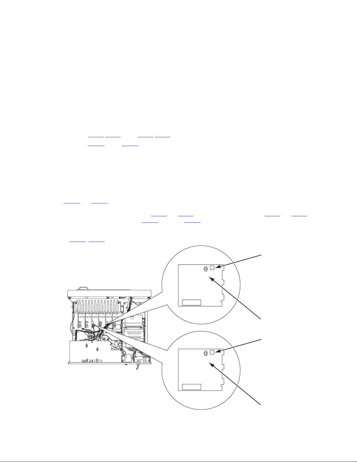
1.4 Critical parts for safety
In regard with component parts appearing on the silk-screen
printed side (parts side) of the PWB diagrams, the parts that are
printed over with black such as the resistor ( ), diode ( )
and ICP ( ) or identified by the " " mark nearby are critical
for safety. When replacing them, be sure to use the parts of the
same type and rating as specified by the manufacturer.
(This regulation dose not Except the J and C version)
each exposed
metal part.
(No.MB303)1-3
Page 4

SECTION 2
SPECIFIC SERVICE INSTRUCTIONS
This service manual does not describe SPECIFIC SERVICE INSTRUCTIONS.
1-4 (No.MB303)
Page 5
SECTION 3
DISASSEMBLY
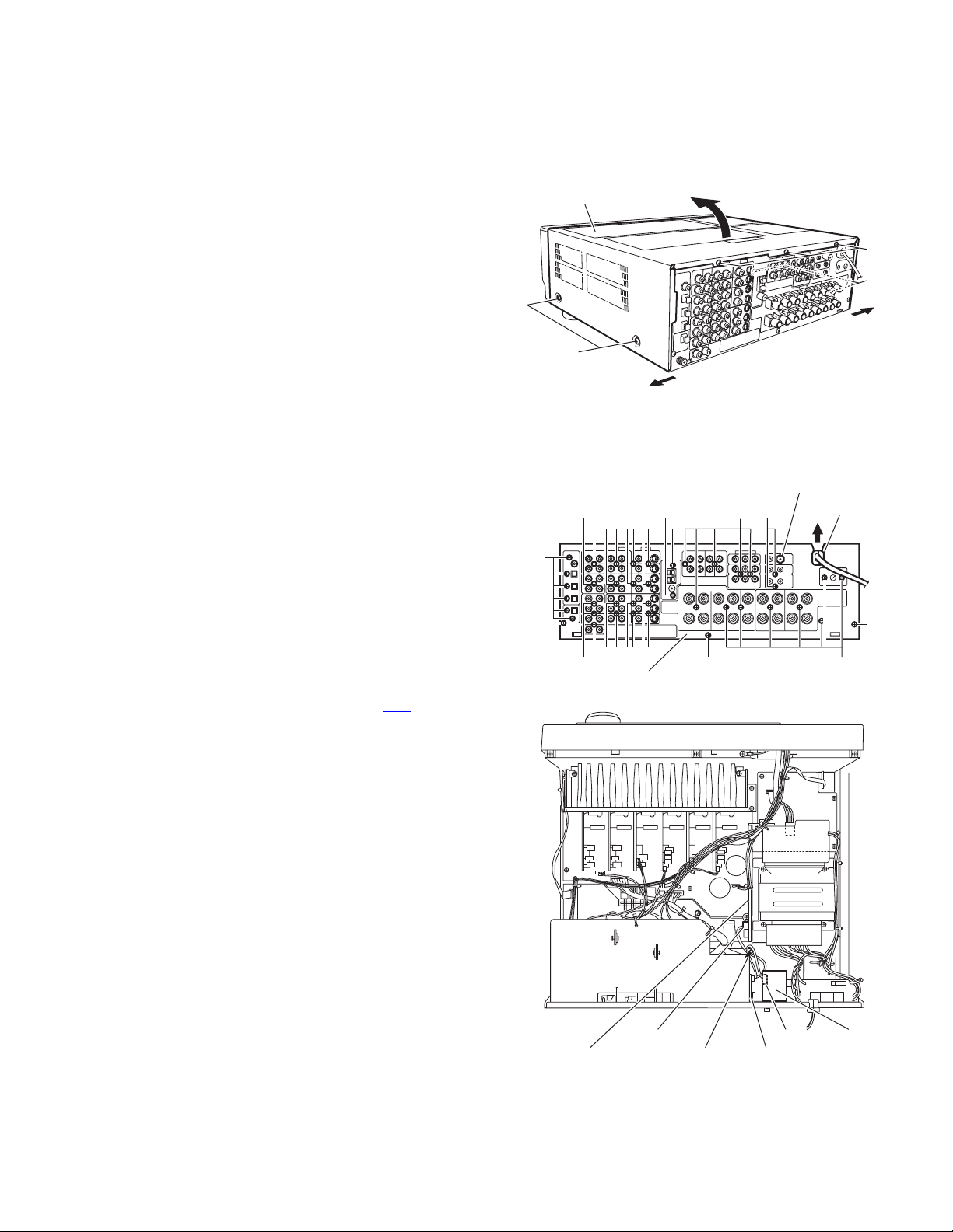
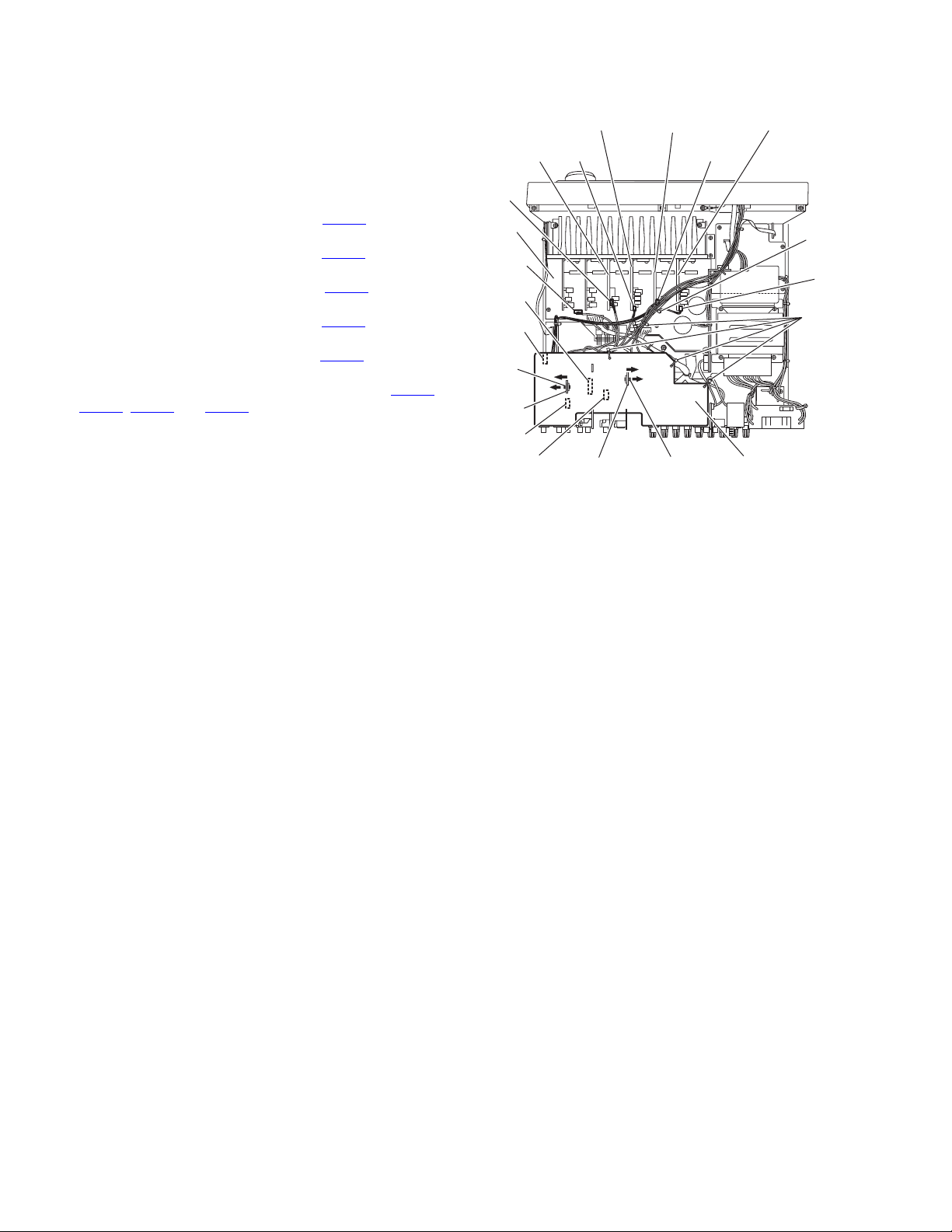
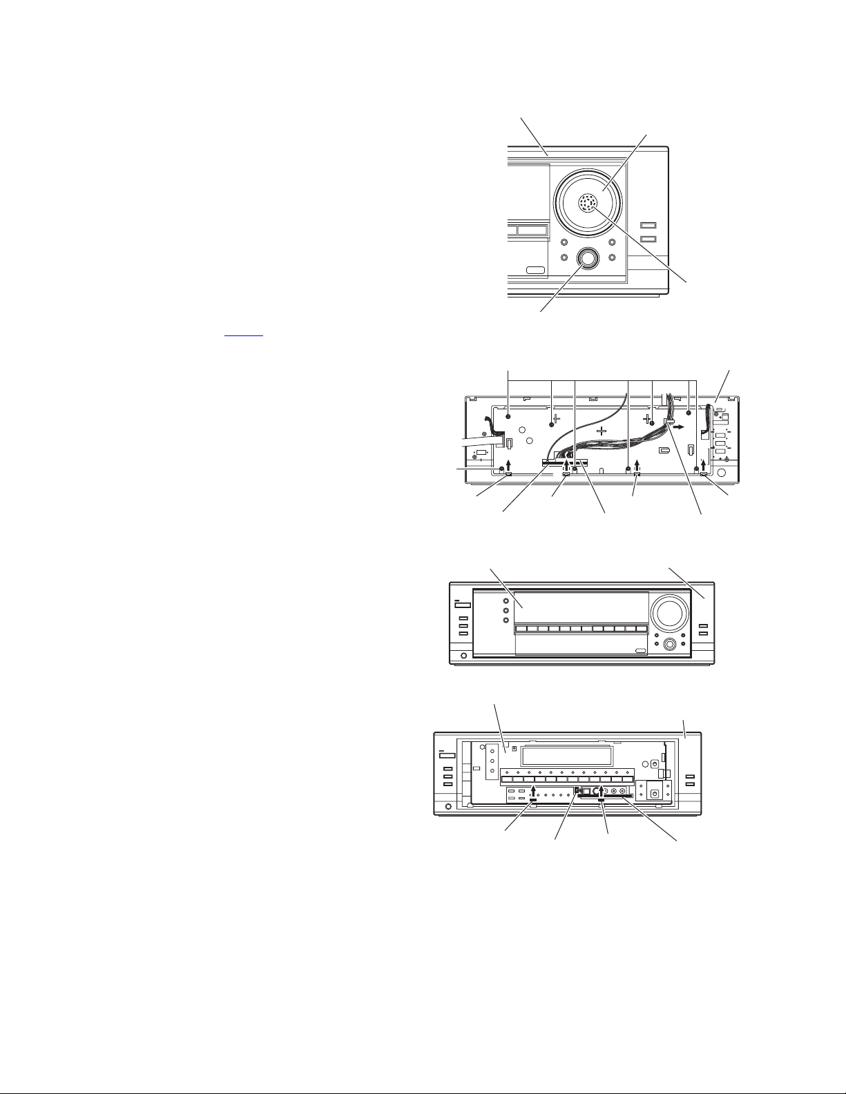
3.1 Removing the top cover (See Fig.1)
(1) From the both sides of the main body, remove the four
screws A attaching the top cover.
(2) From the back side of the main body, remove the three
screws B attaching the top cover.
(3) Remove the top cover in the direction of the arrow 2 while
extending the lower sections of the top cover in the direction of the arrow 1.
3.2 Removing the rear panel (See Fig.2)
• Prior to performing the following procedures, remove the top
cover.
(1) From the back side of the main body, remove the strain re-
lief from the rear panel in the direction of the arrow.
(2) Remove the three screws C, thirty-five screws D, two
screws E, two screws F and nut a attaching the rear panel.
Top cover
A
D
D
2
1
Fig.1
E DDF
B
A
1
Nut a
Strain relief
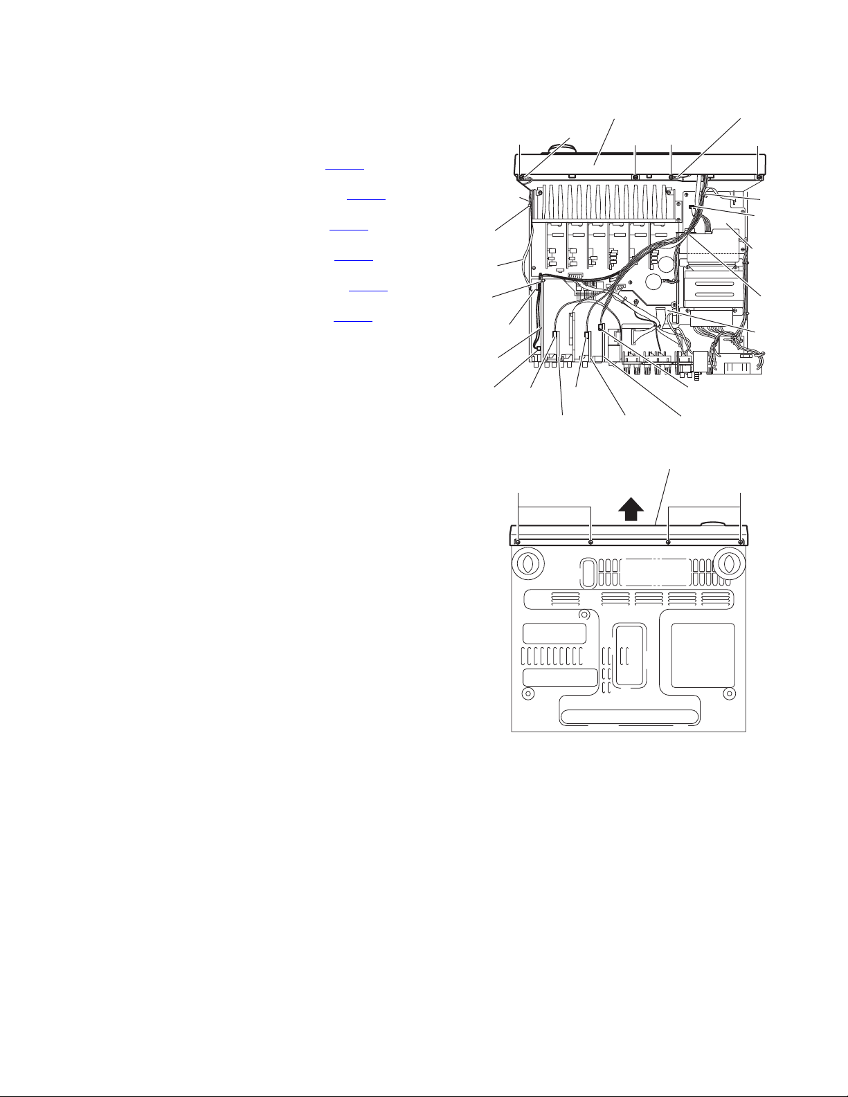
3.3 Removing the RF unit and compu board (See Figs.2 and 3)
• Prior to performing the following procedures, remove the top
cover.
(1) From the top side of the main body, cut off the tie band.
(See Fig.3)
(2) Disconnect the wire from the connector CN1
unit. (See Fig.3)
(3) From the back side of the main body, remove the nut a at-
taching the RF unit. (See Fig.2)
(4) From the top side of the main body, disconnect the wire
from the connector CN262
(5) From the back side of the main body, remove the two
screws F attaching the compu board. (See Fig.2)
on the relay board. (See Fig.3)
on the RF
C
D
Rear panel
Relay board
CN262
C
Fig.2
Tie band
Fig.3
CN1
Compu board
C
RF unit
(No.MB303)1-5
Page 6
3.4 Removing the I/O board (See Fig.4)
• Prior to performing the following procedures, remove the top
cover and rear panel.
(1) From the top side of the main body, remove the two plastic
rivets in the direction of the arrow 1, and remove the stopper boards in the direction of the arrow 2.
(2) Cut off the tie bands bundling the wires.
(3) Disconnect the wire from the connector CN722
on the cen-
ter board.
(4) Disconnect the wire from the connector CN714
on the front
board (L).
(5) Disconnect the wire from the connector CN717
on the sur-
round back board.
(6) Disconnect the wire from the connector CN719
on the front
board (R).
(7) Disconnect the wire from the connector CN723
on the main
board.
(8) Disconnect the I/O board from the connectors (CN205
, CN381 and CN501) in an upward direction.
CN361
Center boardFront board(L)Surround back board
Front
board(R)
CN717 CN714
CN719
Main
board
CN723
CN381
CN501
Plastic
rivet
,
Stopper
2
1
2
1
Tie
band
CN722
Tie
bands
board
CN361
CN205
Stopper board
Plastic rivet
I/O board
Fig.4
1-6 (No.MB303)
Page 7
3.5 Removing the front panel assembly (See Figs.5 and 6)
• Prior to performing the following procedures, remove the top
cover, rear panel and I/O board.
(1) From the top side of the main body, remove the tie bands
bundling the wires. (See Fig.5)
(2) Disconnect the wire from the connector CN599
board. (See Fig.5)
(3) Disconnect the wire from the connector CN415
audio2 board. (See Fig.5)
(4) Disconnect the wire from the connector CN206
eo board. (See Fig.5)
(5) Disconnect the wire from the connector CN244
Video board. (See Fig.5)
(6) Disconnect the card wire from connector CN402
power supply board. (See Fig.5)
(7) Disconnect the card wire from connector CN400
con board. (See Fig.5)
(8) Remove the tie band and wire protection board fixing the
card wire. (See Fig.5)
(9) Remove the two screws G, screws G' and screw H attach-
ing the front panel assembly. (See Fig.5)
(10) From the bottom side of the main body, remove the four
screws J attaching the front panel assembly. (See Fig.6)
(11) Remove the front panel assembly in the direction of the ar-
row. (See Fig.6)
Reference:
When attaching the screw G' and screw H, attach the earth
wire with it.
on the DSP
on the
on the vid-
on the S-
on the
on the mi-
Wire
protection
board
Tie
band
Card
wire
Tie
band
CN400
DSP
board
CN599
Front panel assembly Earth wire
Earth wire
G'
CN206CN415
Audio2 board
GGH
Tie
band
CN402
Power
supply
board
Tie
band
Micon
board
CN244
S-Video boardVideo board
Fig.5
Front panel assembly
JJ
Fig.6
(No.MB303)1-7
Page 8
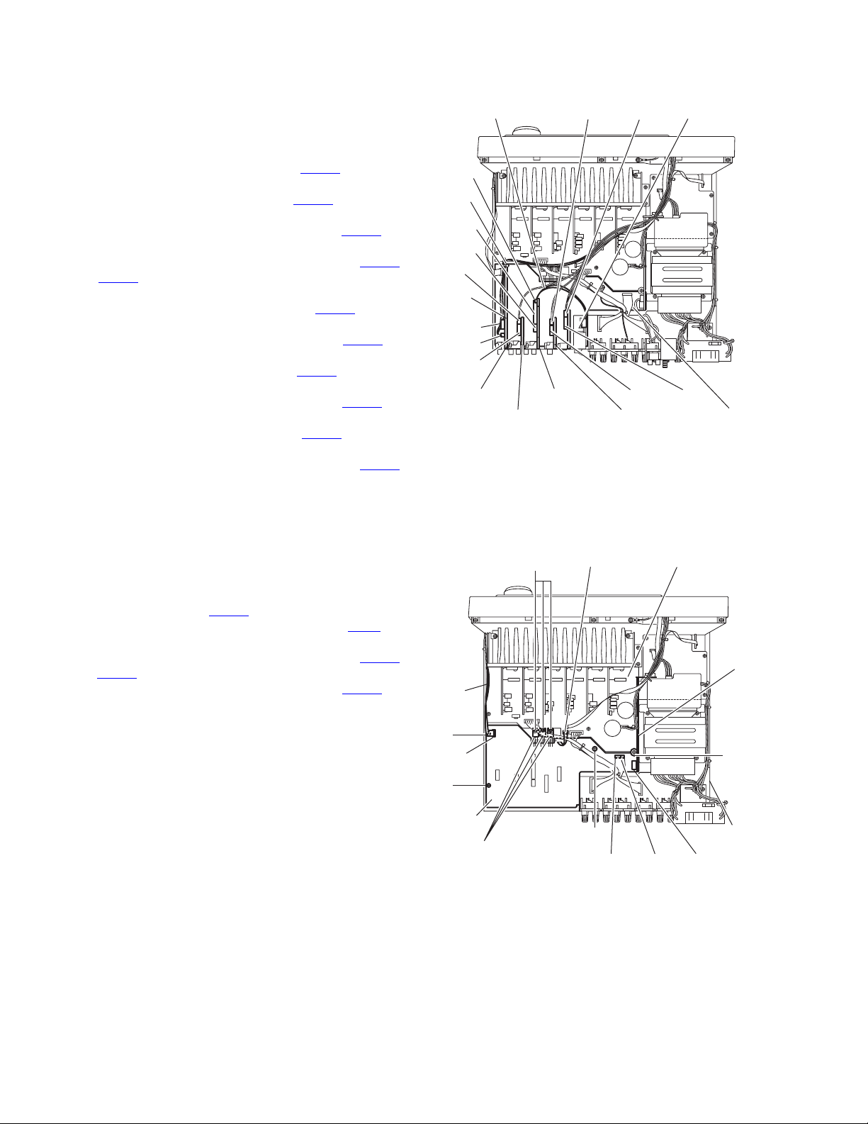
3.6 Removing the tuner, DSP board, Audio board, Audio2 board, Video board and S-Video board
A
(See Fig.7)
• Prior to performing the following procedures, remove the top
cover, rear panel and I/O board.
(1) From the top side of the main body, cut off the tie band bun-
dling the wire.
(2) Disconnect the card wire from connector CN314
dio board, and take out the tuner.
(3) Disconnect the wire from the connector CN599
board.
(4) Disconnect the DSP board from the connector CN601
the micon board, and take out the DSP board.
(5) Disconnect the audio board from the connectors (CN101
and CN303) on the micon board, and take out the audio
board.
(6) Disconnect the wire from the connector CN415
audio2 board.
(7) Disconnect the audio2 board from the connector CN301
the micon board, and take out the audio2 board.
(8) Disconnect the wire from the connector CN206
eo board.
(9) Disconnect the video board from the connector CN201 on
the micon board, and take out the video board.
(10) Disconnect the wire from the connector CN244
Video board.
(11) Disconnect the S-Video board from the connector CN241
on the micon board, and take out the S-Video board.
on the au-
on the DSP
on
on the
on
on the vid-
on the S-
Card wire
CN314
Tie
band
CN303
CN101
CN415
DSP
board
CN601
CN599
CN301
udio2 board
Audio board
CN206 CN244
Video board
CN201 CN241
S-video board
Fig.7
Tuner
Micon board
3.7 Removing the micon board
(See Fig.8)
• Prior to performing the following procedures, remove the top
cover, rear panel, I/O board, tuner, DSP board, Audio board,
Audio2 board, Video board and S-Video board.
(1) From the top side of the main body, disconnect the card
wire from the connector CN400
(2) Disconnect the relay board from the connector CN81 on
the micon board.
(3) Disconnect the parallel wire from the connectors (CN931
and CN932) on the micon board.
(4) Disconnect the parallel wire from the connector CN831 on
the main board.
(5) Remove the three screws K attaching the micon board.
(6) Remove the three screws L attaching the transistors
(Q921, Q931, and Q941) to the chassis base.
(7) Loosen the screw M attaching the micon board.
on the micon board.
L
Card
wire
K
CN400
K
Micon
board
Transistors
(Q921,Q931,Q941)
CN831
K
CN931 CN932
Fig.8
Main board
Relay
board
M
Chassis base
CN81
1-8 (No.MB303)
Page 9
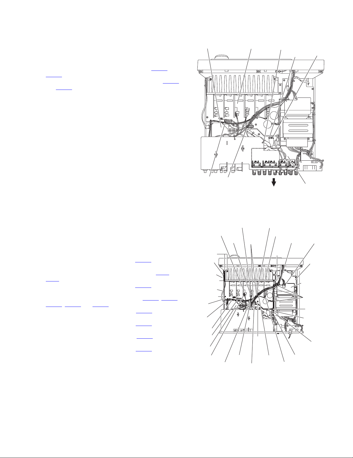
3.8 Removing the speaker board
r
(See Fig.9)
• Prior to performing the following procedures, remove the top
cover, rear panel.
(1) From the top side of the main body, remove the tie band
bundling the wires.
(2) Disconnect the wires from the connectors (CN813
) on the main board.
CN814
(3) Disconnect the parallel wire from the connectors (CN931
and CN932) on the micon board.
(4) Take out the speaker board in the direction of the arrow.
and
Micon board
Main board
Tie band
CN931 CN932
3.9 Removing the relay board and main board
(See Fig.10)
• Prior to performing the following procedures, remove the top
cover.
(1) From the top side of the main body, remove the tie bands
bundling the card wire and wires.
(2) Remove the tie band and wire protection board bundling
the card wire.
(3) Disconnect the wire from the connector CN811
er transformer board 1.
(4) Disconnect the relay board from the connectors (CN71 and
) on the power supply board and micon board.
CN81
(5) Disconnect the wire from the connector CN262 on the relay
board, and take out this board.
(6) Disconnect the wires from the connectors (CN723
CN814, CN831 and CN881) on the main board.
(7) Disconnect the wire from the connector CN722
ter board.
(8) Disconnect the wire from the connector CN714
board (L).
(9) Disconnect the wire from the connector CN717
round back board.
(10) Disconnect the wire from the connector CN719
board (R).
(11) Remove the screw M, six screws N and two screws P at-
taching the main board.
(12) Take out the main board.
on the pow-
, CN813,
on the cen-
on the front
on the sur-
on the front
CN814
Front board(R)
CN813
Surround back board
CN717
N
Tie band
Wire
protection
board
Card wire
Main
board
Tie
band
CN723
CN814
Micon
board
N
P
CN719
CN881
CN831
Fig.9
Front board(L)
Tie band
P
CN714
CN813
Fig.10
Speaker board
Center board
CN71
N
CN81
CN722
CN811
Power
supply
board
Power
transforme
board 1
Tie bands
M
Relay
board
CN262
(No.MB303)1-9
Page 10
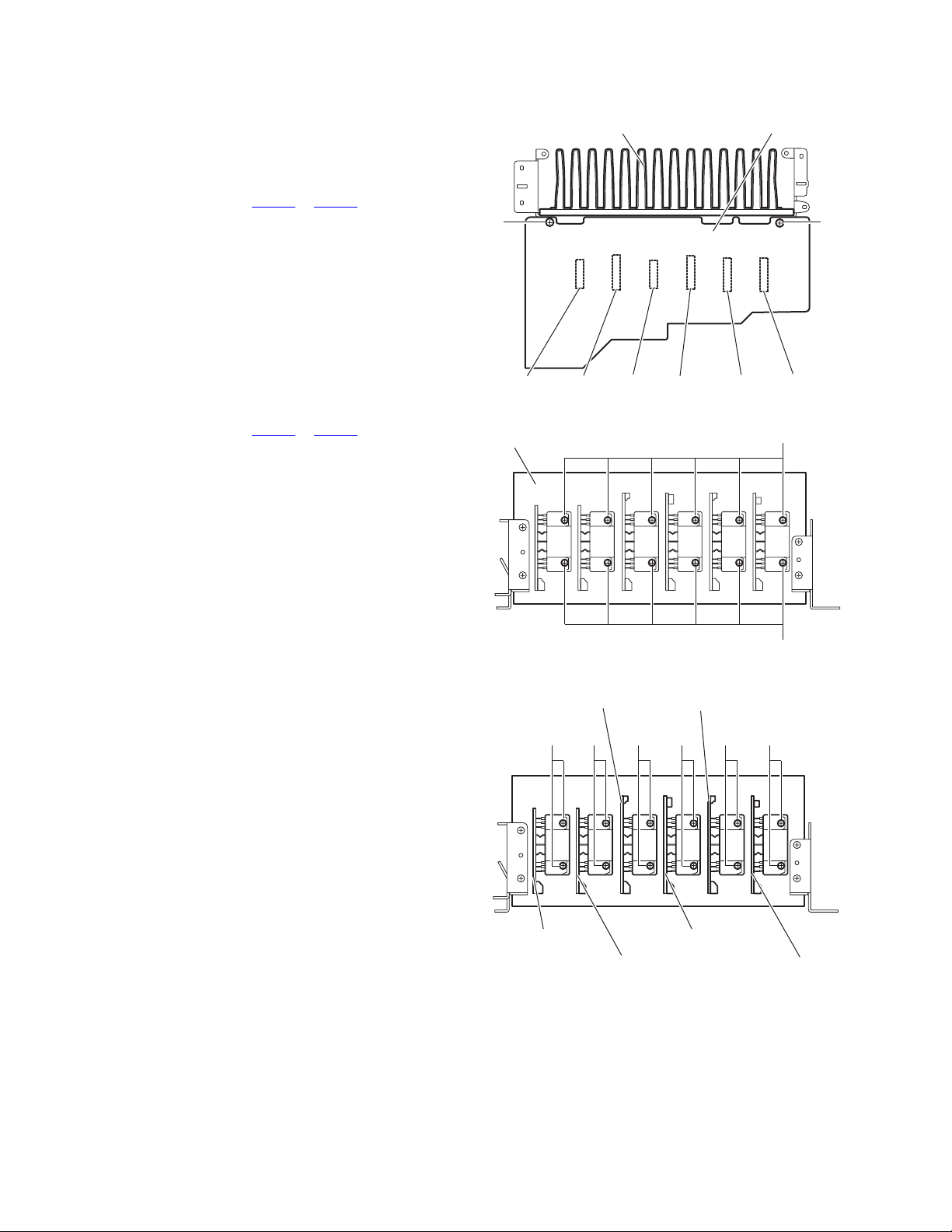
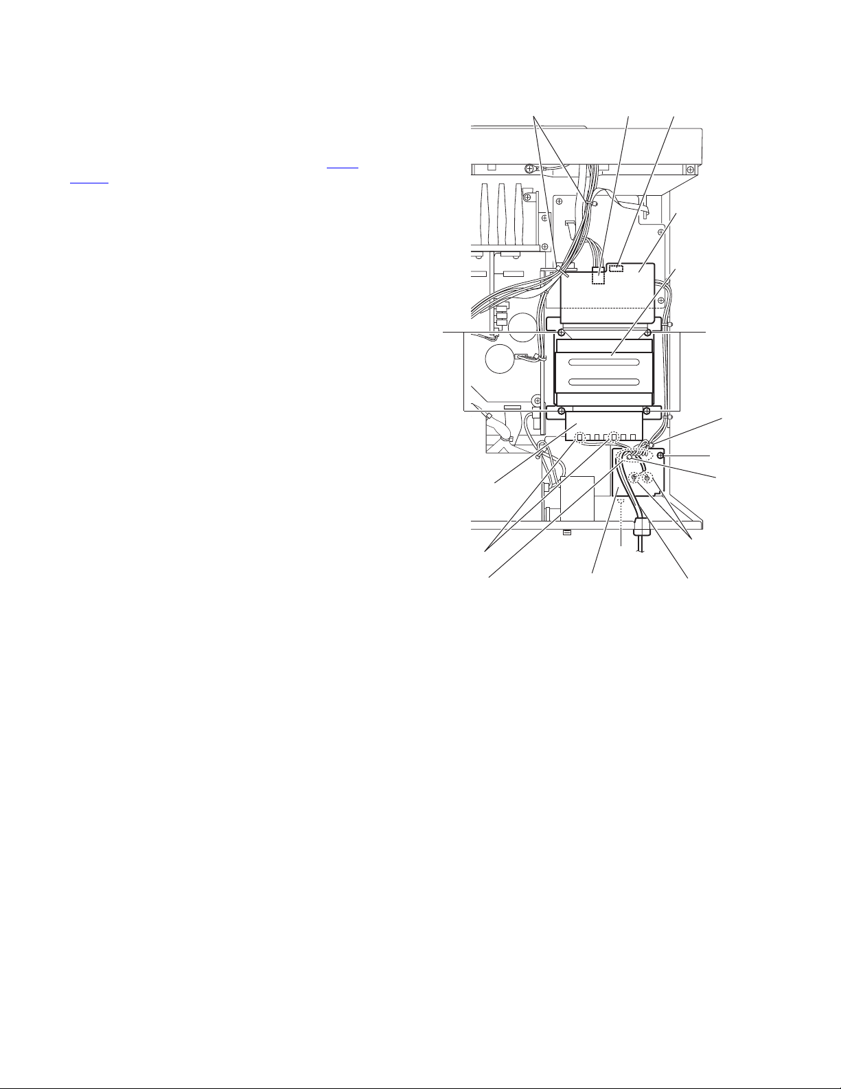
3.10 Removing the heat sink (See Figs.11 and 12)
• Prior to performing the following procedures, remove the top
cover and main board.
(1) From the reverse side of the main board, remove the two
screws Q attaching the main board to the heat sink. (See
Fig.11)
(2) Disconnect the connectors (CN701
board, and remove the main board. (See Fig.11)
(3) Remove the twelve screws R attaching the heat sink. (See
Fig.12)
3.11 Removing the center board, front boards (L/R), surround boards (L/R) and surround back board
(See Figs.11 and 13)
• Prior to performing the following procedures, remove the top
cover and main board.
(1) From the reverse side of the main board, remove the two
screws Q attaching the main board to the heat sink. (See
Fig.11)
(2) Disconnect the connectors (CN701
board, and remove the main board. (See Fig.11)
(3) Remove the two screws R attaching the center board. (See
Fig.13)
(4) Remove the two screws R attaching the front board (L).
(See Fig.13)
(5) Remove the two screws R attaching the surround back
board. (See Fig.13)
(6) Remove the two screws R attaching the front board (R).
(See Fig.13)
(7) Remove the two screws R attaching the surround board
(L). (See Fig.13)
(8) Remove the two screws R attaching the surround board
(R). (See Fig.13)
to CN706) on the main
to CN706) on the main
Heat sink
Main board
Q
CN703 CN701 CN704 CN702 CN705 CN706
Fig.11
Heat sink
Fig.12
Front board(R)
Front board(L)
Q
R
R
R R R R R R
Surround board(R)
Surround board(L)
Surround back board
Center board
Fig.13
1-10 (No.MB303)
Page 11
3.12 Removing the voltage selector board
r
(See Fig.14 and 15)
• Prior to performing the following procedures, remove the top
cover.
(1) From the back side of the main body, remove the two
screws S attaching the voltage board. (See Fig.14)
(2) Remove the solders from the soldered sections b on the
power transformer board 2 and remove the wires of the
voltage selector board. (See Fig.15)
(3) Take out the voltage selector board.
Rear panel
S
Fig.14
Power
transforme
board 2
Tie bands
Soldered sections b
Voltage
selector
board
Fig.15
(No.MB303)1-11
Page 12
3.13 Removing the power transformer
r
r
(See Fig.16)
• Prior to performing the following procedures, remove the top
cover.
(1) From the top side of the main body, remove the tie band
bundling the wires.
(2) Disconnect the wire from the connectors (CN55
) on the power transformer board 1.
CN811
(3) Remove the solders from the soldered sections c on the
power transformer board 2.
(4) Remove the four screws T attaching the power transform-
er.
3.14 Removing the power/fuse board
(See Fig.16)
• Prior to performing the following procedures, remove the top
cover.
(1) From the back side and top side of the main body, remove
the tie band from the bundling the wires and the power
cord.
(2) Remove the screw U and screw V attaching the power/fuse
board.
(3) Remove the solders from the soldered sections d attaching
the power cord.
(4) From the reverse side of the power/fuse board, remove the
solders from the soldered sections e attaching the wires.
and
Power
transformer
board 2
Tie band
CN811 CN55
Power
transforme
board 1
Power
transforme
TT
Tie band
V
Tie band
Soldered
sections c
Soldered sections e
Power/fuse board
Fig.16
U
Soldered
sections d
Power cord
1-12 (No.MB303)
Page 13
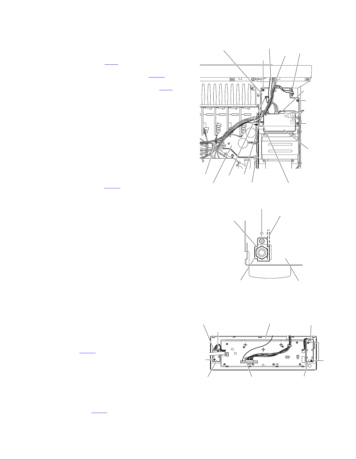
3.15 Removing the power supply board
r
(See Fig.17)
• Prior to performing the following procedures, remove the top
cover.
(1) From the top side of the main body, disconnect the parallel
wire from the connector CN55
board 1.
(2) Disconnect the card wire from the connector CN402
power supply board.
(3) Disconnect the relay board from the connector CN71
the power supply board.
(4) Remove the three screws W attaching the power supply
board.
(5) Remove the power supply board from the hook f of the
chassis base bracket in the direction of the arrow, and take
out the power supply board.
(6) Turn over the power supply board, and remove the solders
from the soldered sections g attaching the wire.
on the power transformer
on the
on
Card wirePower supply board
Tie band
W
Headphone
jack board
CN55
W
Soldered
sections g
W
3.16 Removing the headphone jack board
(See Figs.17 and 18)
• Prior to performing the following procedures, remove the top
cover, rear panel, I/O board and front panel assembly.
(1) From the top side of the main body, disconnect the parallel
wire from the connector CN881
Fig.17)
(2) From the front side of the main body, remove the nut h and
screw X attaching the headphone bracket to the front
bracket. (See Fig.18)
(3) Remove the three screws W attaching the power supply
board. (See Fig.17)
(4) Take out the headphone jack board from the inside of the
chassis base while lifting the power supply board.
3.17 Removing the switch board
(See Fig.19)
• Prior to performing the following procedures, remove the top
cover, rear panel, I/O board and front panel assembly.
(1) From the back side of the front panel assembly, remove the
two screws Y attaching the switch board.
(2) Take out the switch board, and disconnect the wire from
the connector CN432
on the switch board.
on the main board. (See
CN881
CN432
CN402
Main board
Nut h
Headphone bracket
Y
CN71
Relay board
Fig.17
Hook f
X
Headphone jack board
Front bracket
Fig.18
Front panel assembly CN430
Power
transforme
board 1
3.18 Removing the power switch board
(See Fig.19)
• Prior to performing the following procedures, remove the top
cover, rear panel, I/O board and front panel assembly.
(1) From the back side of the front panel assembly, remove the
two screws Z attaching the power switch board.
(2) Take out the power switch board, and disconnect the wire
from the connector CN430
on the power switch board.
Y
Switch board
Front video board
Fig.19
Z
Power switch board
(No.MB303)1-13
Page 14
3.19 Removing the front key & system control board, front video board (See Figs.20 to 23)
• Prior to performing the following procedures, remove the top
cover, rear panel, I/O board, front panel assembly, switch
board and power switch board.
(1) From the front side of the front panel assembly, pull out the
volume and jog knobs, and remove the nut i attaching the
front key & system control board. (See Fig.20)
(2) From the back side of the front panel assembly, remove the
eight screws AA attaching the sub panel assembly. (See
Fig.21)
(3) Remove the wires of the front video board from the hook j
of the front panel assembly in the direction of the arrow 1.
(See Fig.21)
(4) Remove the sub panel assembly while releasing the four
claws k in the direction of the arrow 2. (See Figs.21 and 22)
(5) From the front side of the front panel assembly, disconnect
the wire from the connector CN412
tem control board, and take out the front video board. (See
Fig.23)
(6) Remove the claws m attaching the front key & system con-
trol board in the direction of the arrow and take out the front
key & system control board. (See Fig.23)
on the front key & sys-
Front panel assembly
Jog knob
AA
Volume knob
Nut i
Fig.20
Front panel assembly
1
2
AA
Claw k Claw k Claw k
Front video board
Sub panel assembly
Front key & System control board
2
Sub panel assembly
Fig.21
Fig.22
Claw mClaw m
CN412
Fig.23
2
Claw k
Hook j
Front panel assembly
Front panel assembly
Front video board
2
1-14 (No.MB303)
Page 15
SECTION 4
ADJUSTMENT
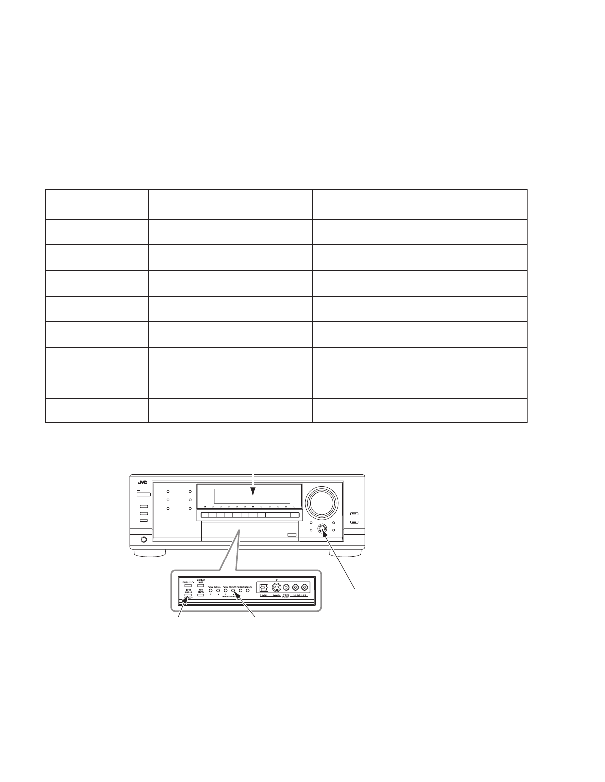
4.1 Test mode
(1) Unplug the power plug.
(2) Insert power plug into outlet while pressing both "PRESET UP" key and "MIDLIGHT" key of the main body.
(3) Then, all segment of the FL display is blinking for 5 seconds, and tuner AM step is switching 9kHz.
(4) The high-speed of volume is checked by remote controller in the test mode.
(5) To release test mode, press "STANDBY/ON" key of the main body.
NOTE:
In the test mode, standby-LED is blinking for every 1 second.
4.2 Power amplifier section
Adjustment of idling current
Measurement location B2204
Adjustment part VR787
-B2205 (Lch) , B2213-B2214 (Rch)
(Lch) , VR788(Rch)
Attention
This adjustment does not obtain a correct adjustment value immediately after the amplifier is used (state that an internal
temperature has risen).
Please adjust, after you turn off amplifier and internal temperature falls.
< Adjustment method >
(1) Set the volume control to minimum during this adjustment. (No signal & No load)
(2) Set the surround mode OFF.
(3) Turn VR787
and VR788 fully counterclockwise to warm up before adjustment.
If the heat sink is already warm from previous use the correct adjustment can not be made.
(4) For L-ch, connect a DC voltmeter between B2204 and B2205 (Lch) and, connect it between B2213 and B2214 (Rch).
(5) 30 minutes later after power on, adjust VR787
for Lch, or VR788 for Rch so that the DC voltmeter value has 1mV to 10mV.
* It is not abnormal though the idling current might not become 0mA even if it is finished to turn variable
resistance (VR787
, VR788) in the direction of counterclockwise.
Front board (L)
VR787
B2204
B2205
VR787 (Lch)
Front board (R)
VR788
B2213
B2214
B2204, B2205 (Lch)
VR788 (Rch)
B2213, B2214 (Rch)
(No.MB303)1-15
Page 16
SECTION 5
TROUBLESHOOTING
5.1 Self-diagnose function
This model incorporates the following self-diagnostic functions.
5.1.1 Starting of self-diagnostic mode
• Insert power plug into outlet while pressing both "PRESET UP" key and "INPUT ANALOG" key of the main body.
Then, "Self-diagnostic mode" starts.
5.1.2 Displaying of state
• When "Self-diagnostic mode" starts, system Micon version is displayed on the FL display.
Each turning MULTI JOG of the main body in the mode changes a state as follows.
FL display (Code)
S0001
D01
D02
D3
D4
D5
D6
D7
FL display State
2004030840
00.00.17
04/02/20
DspRev08
ANALOG02
Fs48kHz
PCM
2/0.0
System Micon version
DSP Micon version
Changed date of version
DSP version
Setting information
Setting information
Setting information
Channel information
FL display
1-16 (No.MB303)
Multi JOG
Preset up keyInput analog key
Page 17

(No.MB303)1-17
Page 18

Victor Company of Japan, Limited
AV & MULTIMEDIA COMPANY AUDIO/VIDEO SYSTEMS CATEGORY 10-1,1chome,Ohwatari-machi,Maebashi-city,371-8543,Japan
(No.MB303)
Printed in Japan
WPC
Page 19
SCHEMATIC DIAGRAMS
AUDIO/VIDEO CONTROL RECEIVER
RX-8040B
CD-ROM No.SML200407
Area suffix
UJ ---------------------- U.S.Military
Contents
Block diagram
Standard schematic diagrams
Printed circuit boards
COPYRIGHT 2004 Victor Company of Japan, Limited.
2-1
2-2 to 11
2-12 to 20
No.MB303SCH
2004/7
Page 20

In regard with component parts appearing on the silk-screen printed side (parts side) of the PWB diagrams, the
parts that are printed over with black such as the resistor ( ), diode ( ) and ICP ( ) or identified by the " "
mark nearby are critical for safety.
Page 21

Block diagram
TO
TUNER
J371
DVD.F-L/R
TV/DBS.L/R
J372
VCR1.REC-L/R
VCR1.PLAY-L/R
J373
VCD2.REC-L/R
VCR2.PLAY-L/R
CD-L/R
J301
TAPE.REC-L/R
TAPE.PLAY-L/R
J302
CDR.REC-L/R
CDR.PLAY-L/R
PHONO-L/R
J303
SUB PREOUT
DVD-C/Y
TV/DBS-C/Y
VCR1R-C/R-Y
VCR1P-C/P-Y
VCR2R-C/R-Y
VCR2P-C/P-Y
MONITOR-C/Y
Audio signal input section
CN314
TUL
TUR
Audio signal input section
FL display section (Front in)
J900
VIDEO, VIDEOC, VIDEOY, VIDEO-L/R, OUT
TUCE, TUCK, TUDI, TUDO
MAIN_STB
MAIN_CLK
MAIN_DATA
IC371
IC375
Source
Selector
SIG.L
SIGR
IC303
AMP.
SUB_STB
SUB_CLK
SUB_DATA
V.SIG.L/R
SUB-L/R
IC307
Sound
IC302
IC306
Source
Selector
FRONT-L
FRONT-R
SUB_DATA
SUB_CLK
SUB_STB
MAIN_DATA
MAIN_CLK
MAIN_STB
SUB-L/R
V.SIG.L/R
VIDEO-L/R
SUB.V_STB
SUB.V_DATA
SUB.V_CLK
Mix
SW_MUTE
FR_RELAY
C_RELAY
SUR_RELAY
SBK_RELAY
CN313
CN315
CN371
CN372
CN312
CN351 CN415
CN906
Video signal input section (S-Video)
J241
J242
J243
J244
Standby LED
S480 to S483
S433, S434
IC241
IC242
C
SW
IC243
IC244
Y
SW
VIDEO1
VIDEO2
VIDEO3
VIDEOC
VIDEOY
VIDEO1
VIDEO2
VIDEO3
CN430
CN432
CN422CN420
System control section
MAIN_STB, MAIN_CLK
MAIN_DATA, TUCE
CN303
TUDI, TUDO, TUCK
SW_MUTE
FR_RELAY, C_RELAY
SUR_RELAY, SBK_RELAY
CN101
CN302
SUB.V_STB, SUB.V_DATA
SUB.V_CLK, SUB_DATA
SUB_CLK, SUB_STB
Q931
MICOM5V REG.
DSP5V REG.
Q941
VIDEO12V REG.
Q981
A+12V REG.
Volume / Video component section
CN381
CN382
FRONT-L/R
CN361
DVD.C
DVD.SW
DVD.LS
DVD.RS
CN244
CN240
J1360
7.1ch
PREOUT
DVD.Y/Pb/Pr
STB.Y/Pb/Pr
MONITOR.Y/Pb/Pr
TV/DBS
VCR1REC
VCR1PB
VCR2REC
VCR2PB
MONITOR
FL display section
KEY1
Q413
Dimmer
STANDBY_LED
KEY1 to 6
DIRECT_LED
CC_CON_LED
Dimmer
S400 to S432
KEY6
Q410, Q411
IC901
System
MICON
DSPA5V, RDS5V, MICON5V
DSP5V, A+12V, A-12V
TU+9V, VIDEO12V, +B2
MAIN_STB, MAIN_CLK
MAIN_DATA, SUB_STB
SUB_CLK, SUB_DATA
SUB-L/R, V.SIG.L/R
IC380
Audio
Source
Selector
IC304, IC386
AMP.
J1490
J1491
J1380
IC361
IC362
IC363
SW
Video signal input section
J201
DVD
J202
J203
J204
IC400
Display
Control
Driver
DSPCLK, DSPREADY, DSPRESET
DSPSTATUS, DSP_COMMAND
HP_RELAY
SUR_RELAY, C_RELAY, SUB_RELAY
F1_RELAY, F2_RELAY, SBK_RELAY
VIDEO1, VIDEO2, VIDEO3, VIDEO4
VOL_STB, VOL_CLK, VOL_DATA
M_RESET, M_BUSY, M_STATUS
M_COMMAND, M_CS, M_CLK
Q921
DSPA5V REG.
RDS5V REG.
Q961
A-12V REG.
Q971
TU+9V REG.
DSP_IN_L, DSP_IN_R
DSP.C, DSP.SW, DSP.SL
DSP.SR, DSP.L, DSP.R
DSP.SrBK
IC396
AMP.
IC381
to
IC384
IC398
AMP.
Volume IC
IC394
VIDEO3
VIDEO4
IC201
VOL_CLK
VOL_STB
VOL_DATA
VIDEO1
VIDEO2
VIDEO3
AMP.
CN205
CN204
VOL_CLK
VOL_DATA
VOL_STB
VIDEO3
VIDEO4
IC202
VIDEO
V
SW
CN206
M_CLK, M_COMMAND, M_STATUS
M_CS, M_BUSY, M_RESET
DCSO, DCSI, VCRO
JOG1
JOG2
RM
JS400
Volume JOG
Q402 to Q404
IC404
Remocon
S1 to S36
G1 to G17
DI400
FL Display
DCS
AV_VCR
POWER_ON
SIG.L
SIG.R
SIG.AMP.SL
SIG.AMP.SR
IC397
AMP.
SIG.C
SIG.SrBK
DCS
AV_VCR
FL1, FL2
-VPP
CN601
FW831
CN931
CN932
CN201
CN204
CN81CN400
CN501
CN734CN732CN731
CN735CN733
CN200
CN410
CN412
DSP IC / Digital signal input terminal section
CN681
DSPRESET, DSPREADY, DSPCOMMAND
DSP_STATUS, DSP_CLK
DSP.L
DSP.R
IC611 to IC613
A4+/B3+/-
Q2101, Q2102, Q2201, Q2202
Q2301, Q3401, Q2501, Q2708
AMP.
A4+/-
A3+/B3+/-
A2+/-, B2+/-
LIN+/-, RIN+/-
CN682
DSP.SrBK
DSP.C
DSP.SW
DSP.LS
DSP.RS
DSP_IN_L
DSP_IN_R
IC651
AMP.
IC632 to IC634
AMP.
IC622
AMP.
IC601, IC602
AMP.
RX4
CN684
Audio amp section
CN714
Q761, Q763
Lch AMP.
CN711
CN701 CN702 CN703 CN704 CN706CN705CN723
Speaker
section
Audio amp section
CN719
Q762, Q764
Rch AMP.
Audio amp section
CN722
Q1751, Q1752
Cch AMP.
Audio amp section
CN717
Q1951, Q1952
SBch AMP.
CN712
CN713
CN718
Audio amp
J1202
COMPULINK
AV COMPULINK
J1203
section
Q1851, Q1853
SLch AMP.
Audio amp
section
Q1852, Q1854
SRch AMP.
CN82
CN262
CN263
DCS
AV_VCR
CN715
CN716
CN72
CN71
CN402
-VPP
+B2, -B2
Primary
section
(Power
transformer 1)
D61 to D64
Q71
-VPP REG.
S.MUTE
IC682
AD/DA
Converter
D/A 0
C_BCK
C_LRCLK
IC667
AD/DA
Converter
terminal
CN55
FW51
PD_DD, RST_DD
96K/48K, 192K/96K
IC673
Compression
D_RST, INT, D_CS, CCLK
CDIN, CDOUT
C_BCK, C_LRCLK, S_BCK
S_LRCLK, DATA, D/A0 to 3
CN831
HP_RELAY
+B, -B
D801
to
D804
RY871
CN801
CN811
Power
Trans.
POWER_ON
B5V
Q52
B5V REG.
D51 to D54
FL1
FL2
IC671
S.MUTE
Digital Signal
Controller
CC_RST
CC_CS
CC_CLK
CCDATA
F1_RELAY, F2_RELAY, C_RELAY
SUR_RELAY, SBK_RELAY
CN824CN823FW931
CN814CN813
Speaker
(Speaker)
Speaker
(Headphone jack)
FW881
CN881
HP_L, HP_R
VS1
Primary section
Q53
RY1
T2
Power
Trans.
MICK
SCK
IC673
RX0
DSP_RST
HREQ
SS, SCK,
MOSI, MISO
GPIO1 to 4
IC661
RX1
RX2
RX3
DSP
TX
RY831
RY832
RY851
RY852
RY853
terminal section
terminal section
Primary
section
(Power/fuse)
J681
DiIGITAL IN1
UN682
DIGITAL IN2
UN683
DIGITAL IN3
UN684
DIGITAL IN4
UN686
DIGITAL OUT
ST831
L(SPK2)
R(SPK2)
L(SPK1)
R(SPK1)
ST851
CENTER
SURR-L
SURR-R
ST852
SURR-BACK
J91
Headphone
jack
Main
plug
2-1
Page 22

Standard schematic diagrams
Primary section
CN82
QGB2510K1-08
CN262
QGA2501C1-06
CN72
QGB2510K1-09
CN402
QGF1205C1-06
CN71
QGB2510J1-09
!
PW20
PW17
PW26
!
PW18
PW28
PW29
PW40
Q42
KTD863/Y/
0.0047
C45
C44
470/16
EP51
F1
TA1
PW19
PW30
TA2
R1
!
3.3M
EP1
D46
MTZJ6.2A
!
CN82 CN71
QGB2510K1-08 QGB2510J1-09
CN402
(SHEET 8)
QGF1205C1-06
CN72
QGB2510K1-09
(SHEET 9)
CN262
QGA2501C1-06
(SHEET 7)
(SHEET 2)
C69
0.047
C68
0.047
R74
100k
C74
CN811
QGA3901F2-03
F61
!
F62
!
R61
10DDA20-FD
!
D63
!
3300/35 1000/35
3.3k
R72
22/50
D61
C65 C66
D73
11ES2-T4
C71
100/63
8.2
11ES2-T4
D62
!
C63
0.1
220/50
D71
11ES2-T4
D72
11ES2-T4
!
C70
CN55
QGD2501C1-05Z
FW51
QUM215-10DGZ4
10DDA20-FD
Q71
KTA1046/Y/
C73
1/50
D75
MTZJ8.2C
Q74
KTC3200/GL/
22/50
R73 D74 C72
MTZJ36C
22k
C52
1000/25
D54
T2
QQT0317-001
!
D52
11ES2-T4
11ES2-T4
1SS133
PW10
PW11
PW12
PW13
PW14
PW15
PW16
!
C1
0.0047
!
Q53
KRC105M
RY1
QSK0098-001
D57
Q52
R53
!
6.8
KTD863/Y/
C55
0.0047
820
R54
C54
470/16
D56
MTZJ6.2B
820
R44
131
3.3
11ES2-T4
D62
!
C63
0.1
1000/35
C70
220/50
D71
11ES2-T4
D72
11ES2-T4
C66
C62C61
0.10.1
D64
11ES2-T4
!
TH71
QAD0095-4R7Z
132
113
112
111
123
122
121
134
133
C51
0.0047/100
D51
11ES2-T4
!
!
D53
11ES2-T4
CN811
QGA3901F2-03
F61
!
F62
!
R61
CN55
QGD2501C1-05Z
C69
0.047
C68
0.047
R74
100k
FW51
QUM215-10DGZ4
10DDA20-FD
!
D61
!
D63
10DDA20-FD
C65
3300/35
D73
Q71
11ES2-T4
KTA1046/Y/
3.3k
C73
22/50
R73 D74 C72
MTZJ36C
22k
R72
C71
100/63
22/50
C74
1/50
D75
MTZJ8.2C
Q74
KTC3200/GL/
C62C61
0.10.1
D64
11ES2-T4
!
TH71
QAD0095-4R7Z
!
131
132
113
112
111
123
122
121
134
133
C51
0.0047/100
D51
11ES2-T4
!
!
11ES2-T4
PW10
PW11
PW21
PW12
PW22
PW23
PW13
PW24
PW14
PW25
PW15
PW16
!
F2
!
T2
C1
QQT0281-004
0.0047
!
!
RY1
QSK0098-001
D52
D57
!
11ES2-T4
1SS133
!
D54
11ES2-T4
C52
470/63
R51
15k
Q51
2SD2394/EF/
R53
!
6.8
R54
R52
C53
3.3k
0.0047
D55
MTZJ12C
!
F4
!
VS1
QSW0812-001
Q53
KRC105M
Q52D53
KTD863/Y/
0.0047
C55
D56
MTZJ6.2B
820
R44
470/16
820
C54
470/16
PW20
PW17PW27
PW26
!
PW18
D46
MTZJ6.2A
F1
PW19
TA1
PW30
TA2
EP1
!
PW28
PW29
PW40
Q42
KTD863/Y/
0.0047
C45
C44
EP51
Parts are safety assurance parts.
When replacing those parts make
sure to use the specified one.
SHEET 1
2-2
Page 23

Speaker terminal section
(SHEET 4) (SHEET 4) (SHEET 3) (SHEET 3) (SHEET 4) (SHEET 7) (SHEET 4)
QJK012-032403
CN801
(SHEET 1)
QGB2510J1-10
COM
0.01
C805
CN704
0.1
C803
0.01
C801
!
D801
30PRA20-FC
D803
!
30PRA20-FC
C807
0.1
C804
0.1
C806
C802
!
D802
30PRA20-FC
!
D804
30PRA20-FC
0.01
C808
6800/71
6800/71
QGB2510J1-10
100k100k
R801R802
CN703
CN701 CN702
QGB2510J1-12
C816
100/25
D816
MTZJ18C
R816
3.3k
12
R815
R811
C811
R812
0.0047
EP801
3.3k
KTC3200/GL/
QGB2510J1-12
2SD2394/EF/
Q812
R830
33
D830
RY832
QSK0109-001
QSK0109-001
RY851
RY852
QSK0109-001
1SS133
C845
R833
R831
33
D831
1SS133
R832
33
1SS133
D832
R851
33
1SS133
D851
R852
33
1SS133
D852
R886
33
1SS133
D853
QUM218-08DGZ4
FW931
10
C835
0.022
10
R885
C885
0.047
10
R888
C888
0.047
C887
0.047
10
R887
10
R889
C895
0.047
C850
4.7/50
D841
MTZJ5.1C
3.9k
R855
R854
100k
220p
C836
R834
C847
220p
D845
1SS133
D846
1SS133
D848
1SS133
Q833
KRC109M
C833
0.022
C834
0.022
220p 220p
0.022
10
C842 C841
220p
C846
10
220p
R837
C843
C837
0.022
0.022
C839
C838
220p
0.022
10
R838
C844
220p
C848
C881
C891
220p
0.001
220p
C886
220p
C890
C892
C884
220p
0.001
220p
C889
C893
C883
220p
0.001
C897
C898
220p
0.01
220p
C894
220p
C896
220p
C899
R868
4.7k
4.7k
4.7k
R861
R858
Q830
KRC109M
R865
4.7k
Q834
KRC109M
ST831
C840
0.022
ST851
ST852
Q832
KRC109M
Q836
KRC109M
Q839
D847
KRC109M
1SS133
R864
C454
4.7k
4.7/50
Q831
KRC109M
C852
4.7/50
R866
4.7k
22k
R862
D843
1SS133
D844
1SS133
D842
1SS133
C851
C853
4.7/504.7/50
R863
Q835
KRC109M
Q837 Q838
KRC109M KRC109M
22K
R867
22k
22k
R859
R856
6.8k
6.8k
6.8k
R857
R860
R869
R870
4.7k
RY830
QSK0109-001
CN705
QGB2510J1-12
Q811
D811
R814
10k
47k
R813
CN723
QGA2501C1-04
10/25
C824
Q825
KTA1268/GL/
10k
R825
Q824
KTC3200/GL/
R823
10k
R826
100k
47/16
Q823
130k
R824
C823
(SHEET 9)
Parts are safety assurance parts.
KTC3199/GL/
CN706
QGB2510J1-12
CN813
QGA3901C1-06
L843
0.45
B6001
CN814
0.45
L844
QGA3901C1-07
B6002
0.45
L845
B6004
0.45
L846
B6003
100k
R841
82k
R842
100k
R843
100k
R844
82k
R845
100k
R846
33
R871
1SS133
D825
CN831
QGD2501C1-04Z
D871
1SS133
RY871
QSK0109-001
CN881
QGD2501C1-03Z
FW881
QUM213-44DGZ4
R91
R92
470
C91
C92
470p
470p
470
EP91
QJK015-063001
CN823
QJK015-073202
CN824
QSK0109-001
J91
QNS0022-001
RY831
QSK0109-001
RY853
When replacing those parts make
sure to use the specified one.
(SHEET 9)
SHEET 2
2-3
Page 24

Audio amp section (1/2)
CN714
QGA2501F1-02
(SHEET 7)
R701 C701
10/35
2.2k
C703 R703
56k
100p
2k
D701
1SS133
C705
100P
Q701
2SC2240-BL/AB/
R707R705
2k
2SC2240-BL/AB/
R709
9.1k
Q703
R733
C711
C751
47p
R761
D771
1SS133
D773
1SS133
R775
R777
10
R771
390
200
200
R773
390
R763
10
C753
47p
150
R721
Q707
KTA1268/GL/
1.5k
R725
Q705
0.01
KTA1268/GL/
220
C717
5.6k
R717
10k
R719
390
R723
390
D703
1SS133
R731
Q709
KTA1268/GL/
C713
68p
22p
C715
68p
C709
10p
R715
56k
R711
Q711
KTC3200/GL/
390
33k
R727
R729
C707
100/16
C745
C741
47/100
47/100
C719
0.0047
VR787
500
R783
620
Q781
2SD637/QR/
R781
390
R789
220
TH783
QAD0012-202
Q771
KTC3200/GL/
Q773
KTA1268/GL/
!
Q761
2SD2390/PY/-F6
R779
0.22
R795
!
Q763
2SB1560/PY/-F6
R787
Q791
KTA1268/GL/
C795
0.022
1k
15k
R797
D791
1SS133
47k
R791
33
L791
1u
R793
10
C791
0.047
C793
0.047
CN711
QGB2510K1-12
CN719
(SHEET 7)
QGA2501F1-03
C702
R702
10/35
2.2k
C704
100p 56k
R704
R706
2k
D702
1SS133
C706
100p
Q702
2SC2240-BL/AB/
R710
9.1k
R708
2k
0.01
C712
220
R734
Q704
2SC2240-BL/AB/
R718
R720
R722
(SHEET 2)
C752
47p
R762
D772
1SS133
KTC3200/GL/
KTA1268/GL/
D774
1SS133
R778
R776
200
200
R772
R774
10
390
390
R764
10
C754
47p
150
Q708
KTA1268/GL/
1.5K
R726
Q706
KTA1268/GL/
5.6k
22p
C718
10k
390
R724
390
D704
1SS133
R732
33k
R728
C716
C714
68p
68p
390
R730
Q710
Q712
KTA1268/GL/
C710
R716
56k
R712
KTC3200/GL/
C708
100/16
VR788
500
R784
620
0.0047
C720
Q782
C742
47/100
2SD637/QR/
R782
390
10p
R790
220
TH784
QAD0012-202
Q772
Q774
!
Q762
2SD2390/PY/-F6
R780
0.22
R796
!
Q764
2SB1560/PY/-F6
R788
Q792
KTA1268/GL/
C796
0.022
1k
15k
R798
D792
1SS133
47k
R792
33
L792
1u
R794
10
C792
0.047
C794
0.047
Parts are safety assurance parts.
When replacing those parts make
C746
47/100
sure to use the specified one.
2-4
(SHEET 2)
CN712
QGB2510K1-12
SHEET 3
Page 25

Audio amp section (2/2)
CN722
QGA2001F1-02
(SHEET 7)
R1721
C1713
R1703
2k
D1701
1SS133
C1701
R1701
2.2k
C1703
1/50
Q1701
2SC2240-BL/AB/
R1705
12k
R1702
C1702
56k
100p
Q1702
2SC2240-BL/AB/
R1712
56k
C1705
5p
R1711
C1704
100/16
220
100/16
Q1703
KTA1268/GL/
C1711
33p
C1712
0.01
270
R1733
R1722
3.3k
R1723
3.3k
Q1731
2SD637/QR/
TH731
QAD0012-202
C1715
47/50
R1724
3.3k
R1725
3.3k
C1743
47/100
D1771
910390
R1731
1SS133
Q1771Q1772
R1732
KTC3200/GL/KTA1268/GL/
D1772
1SS133
R1741
220
C1751
R1751
47p
10
R1773
200
R1774
200
2SB1560/PY/-F6
R1752
10
!
Q1751
2SD2390/PY/-F6
R1771
390
R1753
0.22
R1772
R1791
1k
390
Q1752
!
D1791
1SS133
C1752
47p
R1795
47k
Q1791
KTA1268/GL/
R1761
C1791
33
0.022
L1761
R1762
0.45u
R1793
18k
10
C1761
0.047
C1762
0.047
C1741
47/100
CN713
QGB2510K1-10
CN717
QGA2001F1-03
(SHEET 7)
C1901
R1901
1/50
2.2k
C1902
100p
D1901
1SS133
C1903
2SC2240-BL/AB/
R1902
56k
R1903
2k
R1912
56k
Q1902
2SC2240-BL/AB/
C1905
5p
R1911
C1904
100/16
Q1901
R1905
12k
(SHEET 2)
R1821
C1815
R1805
2k
D1801
1SS133
C1801
R1801
2.2k
C1805
1/50
Q1801
2SC2240-BL/AB/
R1809
12k
R1803
C1803
56k
100p
Q1803
2SC2240-BL/AB/
R1813
56k
C1809
5p
R1811
C1807
100/16
220
100/16
Q1805
KTA1268/GL/
C1811
33p
C1813
0.01
270
R1835
R1823
3.3k
R1825
3.3k
Q1831
2SD637/QR/
TH831
QAD0012-202
C1817
47/50
R1827
3.3k
R1829
3.3k
D1871
910390
1SS133
R1831R1833
Q1871Q1873
KTC3200/GLKTA1268/GL/
D1873
1SS133
R1853
R1851
10
10
R1875
200
R1877
200
2SB1560/PY/-F6
C1851
47p
!
Q1851
2SD2390/PY/-F6
R1871
390
R1855
0.22
R1873
R1891
1k
390
Q1853
C1853
47p
R1893
!
D1891
1SS133
R1895
47k
Q1891
KTA1268/GL/
R1861
C1891
33
0.022
L1861
R1863
0.45u
10
18k
C1861
0.047
C1863
0.047
C1841
47/100
R1802
2.2k
C1804
100p
R1806
2k
D1802
1SS133
C1802
C1806
1/50
Q1802
2SC2240-BL/AB/
R1810
12k
R1804
56k
Q1804
2SC2240-BL/AB/
R1814
56k
C1810
5p
R1812
C1808
100/16
R1921
C1913
220
100/16
Q1903
KTA1268/GL/
C1911
33p
C1912
0.01
270
R1933
R1922
3.3k
R1923
3.3k
Q1931
2SD637/QR/
TH901
QAD0012-202
C1915
47/50
R1924
3.3k
R1925
3.3k
C1943
47/100
D1971
910390
R1931
1SS133
Q1971Q1972
R1932
KTC3200/GL/KTA1268/GL/
D1992
1SS133
R1941
220
C1951
47p
R1951
10
R1973
200
R1994
200
2SB1560/PY/-F6
R1952
10
!
Q1951
2SD2390/PY/-F6
R1971
390
R1953
0.22
R1991
R1972
Q1952
1k
390
C1952
47p
R1993
!
D1993
1SS133
R1995
47k
Q1991
KTA1268/GL/
R1961
C1991
0.022
18k
33
L1961
R1962
0.45u
10
C1961
0.047
C1962
0.047
C1941
47/100
CN718
QGB2510K1-10
(SHEET 2)
R1822
C1816
220
100/16
Q1806
KTA1268/GL/
C1812
33p
C1814
0.01
270
R1836
R1824
3.3k
R1826
3.3k
Q1832
2SD637/QR/
TH832
QAD0012-202
C1818
47/50
R1828
3.3k
R1830
3.3k
D1872
910390
R1832R1834
1SS133
Q1872Q1874
KTC3200/GL
KTA1268/GL/
D1874
1SS133
R1852
R1854
10
R1876
R1878
200
10
200
2SB1560/PY/-F6
C1852
47p
!
Q1852
2SD2390/PY/-F6
R1872
390
R1856
0.22
R1874
R1892
1k
390
Q1854
!
D1892
1SS133
C1854
47p
R1896
47k
Q1892
KTA1268/GL/
R1862
C1892
33
0.022
L1862
R1864
0.45u
R1894
18k
10
C1862
0.047
C1864
0.047
C1842
47/100
C1843
R1841
47/100
220
CN715
QGB2510K1-12
(SHEET 2)
C1844
R1842
47/100
220
CN716
QGB2510K1-12
(SHEET 2)
Parts are safety assurance parts.
When replacing those parts make
sure to use the specified one.
SHEET 4
2-5
Page 26

Audio signal input section
R323
TAPE.REC-L
470
R325
TAPE.PLAY-L
470
R327
CDR.REC-L
470
R329
CDR.PLAY-L
QNN0546-001
QNN0215-001
J302
J303
470
R1261 R1262
470 470
C301
4.7/50
R301
2.2k
R302
2.2k
C302
4.7/50
R305
47k47k
100p100p
620
C303C304
R303R304
100/10 100/10
C314 C313
R306
620
R1259
68
IC308
NJM4565M
C1243
R335
R336
SUB_PRE
68
68
TAPE.REC-R
TAPE.REC-L
4.7/50
R1243
100k
R1244
100k
4.7/50
TAPE.PLAY-R
TAPE.PLAY-L
C1244
CDR.REC-L CDR.REC-R
R1239
5.1k
R1240
5.1k
CDR.PLAY-R
CDR.PLAY-L
IC308
NJM4565M
VIDEO-R
VIDEO-L
R324
TAPE.REC-R
470
R326
TAPE.PLAY-R
470
R328
CDR.REC-R
470
R330
CDR.PLAY-R
470
IC301
NJM1580D-D
IC301
NJM4580D-D
C305 C307
0.0018 0.0068
R307 R309
39k 470k
C306
0.0018
R308 R310
39k 470k
100p100p
C309C310
C308
0.0068
2SC3576-JVC-T
Q1247
2SC3576-JVC-T
R1254 R1248
C311
4.7/50
R311R312
C312
4.7/50
1k0
R1247R1253
R1249
10k
R1250
10k
Q1248
01k
Q1245
KRA104M
R315
330
PHONO-L
C315C316
47/1647/16
100k100k
PHONO-R
R316
330
C1245
22/50
R1245
1k
22/25
C335
IC302
TC9164AF-X
22/25
C336
C1241
4.7/50
R1241
C1259
100k
47/25
R1237J301
1.2kQNN0018-002
R1238
1.2k
R1242
100k
C1260
47/25
C1242
4.7/50
R1260
68
PHONO-R
V.SIG.R
V.SIG.L
PHONO-L
SUB-L
SUB-R
C339
560p
IC306
NJM4565M
C1221
10/50
100k100k
R1223R1224
R1221R1222
C1222
10/50
NJM4565M
C1223
10/50
R1225
100k
100k100k
R1226
100k
C1224
10/50
IC306
68
R1265
22/25
C1265
R1266
IC305
C1266
22/25
68
TC9164AF-X
TAPE.PLAY-R
TAPE.PLAY-L
CDR.PLAY-R
CDR.PLAY-L
R1227
R1228
VIDEO-RVIDEO-L
R1229
100k
C1227C1225
4.7/5047/25
68
IC307
TC9459F-X
68
C1226
C1228
47/25
4.7/50
R1230
100k
PHONO-R
SUB-R
SIG.AMP.SR
SURR.SIG.R
SUB.SIG.R
PHONO-L
SUB-L
SURR.SIG.L
SIG.AMP.SL
C1231
220p
SUB.V_STB
SUB.V_DATA
SUB.V_CLK
C1269
560p
SUB_MUTE
R1231
1k
C1229
4.7/50
C1230
4.7/50
C1232
22/50
KRA104M
C1233
10/50
R1232
470k
R1233
1k
Q1231
R1235
10k
Q1233
2SC3576-JVC-T
R1236
10k
Q1234
2SC3576-JVC-T
R1234
1k
QNN0018-002
QNN0018-002
QNN0546-001
VIDEO-R
VIDEO-L
CN415 CN351
QGA2501F1-03 QGB1214K1-16S
SIG.AMP.SR
SIG.AMP.SL
SURR.SIG.R
SURR.SIG.L
SUB-R
SUB-L
V.SIG.R
V.SIG.L
SUB.V_STB
SUB_MUTE
SUB.V_DATA
SUB.V_CLK
SUB_PRE
CN311CN312
QGB2510K1-04QGB1214K1-08S
(SHEET 8) (SHEET 7) (SHEET 9) (SHEET 9)
CN314
QGF1205F1-11
TUCE
220
R398
R392
R394
Q302
2SC3576-JVC-T
R371 R372
DVD.F-L
470 470
R373
470
J371
J372
J373
TV/DBS-L
VCR1.REC-L
VCR2.PLAY-L
CD-L
R375
470
R377
470
R379
470
R381
470
R317
470
DVD.F-R
R374
470
TV/DBS-R
R376
470
VCR1.REC-R
R378
470
VCR1.PLAY-RVCR1.PLAY-L
R380
470
VCR2.REC-RVCR2.REC-L
R382
470
VCR2.PLAY-R
R318
470
CD-R
IC371
TC9163AF-X
R385
68
C385
22/25
22/25
DVD.F-R
VCR1.REC-R
TV/DBS-R
VCR1.PLAY-R
C386
VCR1.REC-L
TV/DBS-L
DVD.F-L
R386
68
VCR1.PLAY-L
VCR2.REC-R
VCR2.REC-L
VCR2.PLAY-RVCR2.PLAY-L
CD-R
V.SIG.R
C389
560p
CD-L
V.SIG.L
C1271
22/25
IC375
TC9163AF-X
R1271
68
VCR1.PLAY-R
DVD.F-R
TV/DBS-R
C1272
22/25
R1272
68
DVD.F-L
TV/DBS-L
VCR2.PLAY-RVCR2.PLAY-L
VCR1.PLAY-L
CD-R
R341R342
C1275
CD-L
560p
IC303
NJM4565M
C341
10/16
100k100k
100k100k
R343
R344
C342
10/16
IC303
NJM4565M
C352
6.8k
R352
0.0056
FL352
C343
10/16
C344
10/16
QQR1372-001
100k 100k
R346 R345
FL351
QQR1372-001
R396
10k
Q303
KRA104S-X
TUMUTE
R397
C399
1k
22/16
R395
10k
Q301
2SC3576-JVC-T
TUDI
TUCK
TUDO
TUL
1k
1k
TUR
CN371
QGB1214K1-18S
V.SIG.L
V.SIG.R
S_MUTE
SW_MUTE
SBK.1SPK
FR_RELAY
C_RELAY
SUR_RELAY
SBK_RELAY
2-6
CN372
QGB1214K1-06S
R351
6.8k
C351
0.0056
SBK.1SPK
CN313
QGB2510K1-17
FR_RELAY
C_RELAY
SUR_RELAY
SBK_RELAY
CN315
QGB2510K1-04
(SHEET 9)(SHEET 9)(SHEET 7)(SHEET 7)
SHEET 5
SW_MUTE
TUMUTE
S_MUTE
TUCE
TUDI
TUCK
TUDO
Page 27

Video signal input section
C200
R207
R200
330
J201J202J203J204
QNN0011-001QND0011-001QNN0011-001QNN0017-002
75
R201
75
C226
47p
R202
75
R203
75
C227
47p
R204
75
R205
75
R206
75
C228
47p
4.7/50
C201
R208
330
4.7/50
C202
470/6.3
C203
R210
330
4.7/50
C204
470/6.3
C205
R212
330
4.7/50
C206
470/6.3
CN200
QGB2510K1-12
2.2
C211
0.01
C231
C208
C234
C230
C212
C233
IC202 IC201
NJM2246M-X MM1117XF-XE
C232
C235
390
R215
C209
R216
Q201
KTA1267/YG/-T
Q202Q205
KRC107S-XKRC107S-X
390
R218
C210
R219
Q204
KTA1267/YG/-T
390
R221
Q207
KTA1267/YG/-T
4.7/50
0.01
C213
47/16
470
R217
10k
Q203
KRC107S-X
470
R220
10k
Q206
KRC107S-X
C207
4.7/50
330
R214
CN206
QGA2501F1-02
CN204
QGB1214K1-10S
R225
2.2
R226
GND
C298
DBS-C
C296
VCR2.P-C
DVD-C
C299
VCR1.P-C
180
R276
180
R277
(SHEET 9)
J241
J243
QND0098-001
J244 J242
QND0107-001 QND0098-001 QND0108-001
DVD-C
C240
757575 757575
R240R242R246 R241R243R247
C268
R244
47P
68
R245
C269
75
47p
C270
R248
47p
68
R249
C271
75
47p
7575
R250R251
C272
R252
47p
68
R253
C273
75
47p
0.01
47p47p47p47p47p47p47p47p
C260C261C262C263C264C265C266C267
470/6.3
470/6.3
470/6.3
DVD-Y
C241
4.7/50
DVD_S/C
DBS-C
C242
0.01
DBS-Y
C243
4.7/50
DBS_S/C
C244
0.01
C245
VCR1.P-C
C246
0.01
VCR1.P-Y
C247
4.7/50
VCR1_S/C
C248
0.01
C249
VCR2.P-C
C250
0.01
VCR2.P-Y
C251
4.7/50
VCR2_S/C
C252
0.01
C253
C297
C275
IC241
MM1113XF-X
IC242
MM1114XF-X
R267
390
R261
Q241
KTA1267/YG/-T
Q242Q245
KRC107S-XKRC107S-X
390
R264
Q244
KTA1267/YG/-T
390
Q247
KTA1267/YG/-T
C282
0.01
DBS-Y
C256 C257
0.01 4.7/50
C283
0.01
C276
47/16
C280
470
R262
10k
R263
Q243
KRC107S-X
C281
470
R265
10k
R266
Q246
KRC107S-X
0.01
C254
C274
10p
VIDEOY
VIDE0C
C284
C255
4.7/50
CN244
QGA2501F1-04
C294
VCR2.P-Y
DVD-Y
C292
VCR1.P-Y
C291
C290
IC244 IC243
C295
MM1117XF-XE
NJM2246M-X
R268
Q248
KTA1267/YG/-T
Q249
KRC107S-X
R271
Q251
KTA1267/YG/-T
Q252
KRC107S-X
R274
Q254
KTA1267/YG/-T
C287
0.01
C288
0.01
C293
C289
47/16
390
C285
470
R269
10k
R270
Q250
KRC107S-X
390
C286
470
R272
10k
R273
Q253
KRC107S-X
390
2.2
R275
DVD_S/C
DBS_S/C
VCR1_S/C
VCR2_S/C
QGB2510K1-09
GND
CN240
(SHEET 9)
(SHEET 7)(SHEET 8)
(SHEET 8)
SHEET 6
2-7
Page 28

Volume / Video Component section
CN261
QJK017-030503
CN263
(SHEET 1)
QJK005-061201
CN205
QGB1214J1-10S
VIDEO3
VIDEO4
VOL_DATA
VOL_CLK
VOL_STB
(SHEET 6)
CN501
QGB1214J1-14S
DSP_IN_L
DSP_IN_R
DSP.L
DSP.R
DSP.LS
DSP.RS
DSP.C
DSP.SW
(SHEET 10)
CN381
QGB1214J1-18S
V.SIG.L
V.SIG.R
FRONT-L
FRONT-R
MAIN_STB
MAIN_CLK
MAIN_DATA
S_MUTE
SW_MUTE
SBK.1SPK
(SHEET 5)(SHEET 5)
FR_RELAY
C_RELAY
SUR_RELAY
SBK_RELAY
SUB_STB
SUB_CLK
SUB_DATA
SUB-L
SUB-R
CN382
QGB1214J1-06S
SUB_STB
SUB_CLK
SUB_DATA
SIG.AMP.SR
SIG.AMP.SL
SURR.SIG.R
SURR.SIG.L
SUB-R
SUB-L
MAIN_STB
MAIN_CLK
MAIN_DATA
(SHEET 5)
V.SIG.R
V.SIG.L
CN361
QGB1214J1-16S
J1360
QNN0548-001
VIDEO3
C1202
R1213
560
C1204
100/10
0
R1530
R1361
C1361
390p390p
C1362
R1362
560
R333
470
C333
390p
C334
390p
R334
470
D1202D1201
1SS3551SS355
R1202
39k
KRA107M
R1201
39k
1000p
C1201
R1208
1k
1.5k
R1209
LINKGND
MA3062/H/-X
D1203
C1363
4.7/50
R1363R1364
100k100k
C1364
4.7/50
C361
4.7/50
100k100k
R361R362
C362
4.7/50
IC386
NJM4565M
C1365
R1365R1366
R363
R364
4.7/50
100k100k
C1366
4.7/50
IC386
NJM4565M
IC304
NJM4565M
C363
4.7/50
100k
C364
100k
4.7/50
IC304
NJM4565M
R1203 R1206
R1205
100k 10k
100k
IC261
NJM2406F-X
R1204
27k
Q1202
KTA1273/Y/-T
470
R1210
220
R1211
R1212
R1369
1k
DVD-C
R1367R1368
9.1k
DVD-SW
R367
1k
R365R366
9.1k9.1k
R368
1k
100/10
K1
QQR0779-001Z
C1205
220p
220
C1203
0.1
J1201
QNS0186-001
J1202
QNS0089-001
R1312
100k
J1203
QNS0089-001
IC381
TC9459F-X
R1301
68
C1301
47/25
2.2k
2.4k
R1306
R1308
DSP_IN_R
1k
DSP.SW
DSP.C
R1304
MAIN_CLK
MAIN_DATA
MAIN_STB
C1303
220p
1k
R1303
DSP_IN_L
2.4k
2.2k
R1305
R1307
IC382
TC9459F-X
IC383
TC9459F-X
TC9459F-X
IC384
DSP.RS
DSP.R
FRONT-RFRONT-L
IC380
TC9162AF-X
DSP.L
DSP.LS
C1302
47/25
R1302
68
R1372
1.1k
R1371
1k
C1312
4.7/50
C1314
4.7/50
C1313
C1311
100k
R1311
R1322
100k
C1322
4.7/50
C1324
4.7/50
C1323
C1321
R1321
100k
R1332
100k
C1332
4.7/50
C1334
C1333
4.7/50
R1331
100k
4.7/50
C1343
100k
R1341
C1499Q1201
1.5
4.7/50
C1316C1326C1325
0.22/500.22/500.22/50
C1319
220p
VOL_STB
VOL_DATA
VOL_CLK
C1315
0.22/50
4.7/50
4.7/50
C1329
220p
VOL_STB
VOL_DATA
VOL_CLK
4.7/50
4.7/50
C1339
220p
VOL_STB
VOL_DATA
VOL_CLK
C1331
4.7/50
C1349
220p
VOL_STB
VOL_DATA
VOL_CLK
4.7/50
C1341
S_MUTE
VIDEO4
IC361
C1373
100/10
C1310
R1310
22/16
1k
Q1310
KRA104S-X
R1309
470k
R1335
10k
R1336 R1464
10k
R1490
R1487
10k
2SC3576-JVC-T
SBK.1SPK
MM1504XN
R1375
Q1374
R1471
R1502
R1511
Q1490
KRA104S
620
R1376
100
Q1375
KRC107S-X
68
R1419
C1411
10/50
100k
R1411
100k
R1412
C1412
10/50
R1420
68
R1439
C1431
4.7/50
100k
R1431
C1439
47/25
100k
R1432
C1440
47/25
68
R1440
C1451
10/50
100k100k
R1451R1452
C1452
10/50
SUR_RELAY
100k
R1475
5.1k
R1473
1.2k
R1506
0
R1504
0
SBK_RELAY
0
R1515
0
R1513R1474
R1476
15k
1.6k
470K
C1371 C1372
0.01 0.01
C1368
10p
R1377
47
KTA1267/YG/-T
C1419
47/25
R1413R1414
1.2k1.2k
C1420
47/25
FR_RELAY
R1435
10k
1.2k
R1433
R1436
5.1k
1.2k
R1434
C_RELAY
R1455
5.1k
R1453R1454
1.2k1.2k
R1456
5.1k
IC395
NJM4565M
IC395
NJM4565M
IC394
NJM4565M
C1474
47/35
IC394
NJM4565M
R1342
10k
2SC3576-JVC-T
C1370
0.01
C1367
10p
R1374
47
KTA1267/YG/-T
R1313
1k
R1315
10k
Q1313
2SC3576-JVC-T
2SC3576-JVC-T
Q1314
R1316
10k
R1314
1k
C1309
10/50
R1326
10k
Q1324
R1324
2SC3576-JVC-T
1k
C1432
10/50
R1333
1k
Q1333
2SC3576-JVC-T
Q1334
2SC3576-JVC-T
R1334
1k
C1471
10/50
1k
Q1492
R1343
C1344
22/16
R1415
R1416
IC397
NJM4565M
IC397
NJM4565M
IC398
NJM4565M
IC398
NJM4565M
C1473
10/50
KRC107S-X
Q1491
IC362
MM1502XN
5.1k
5.1k
Q1448
KRC107S-X
Q1468
KRC107S-X
R1477
Q1488
R1478
R1486
R1378
Q1376
IC396
NJM4565M
IC396
NJM4565M
C1434
10/50
C1454
10/50
470
KRC107S-X
SW_MUTE
100k
100k
510
R1472
510
Q1428
C1453
10/50
KRA104S-X
C1413
10/50
C1414
10/50
C1433
4.7/50
R1437
R1438
KRA104S-X
R1457R1458
KRA104S-X
Q1489
R1489
R1379
130
Q1449
R1449
Q1469
R1469
Q1377
KRC107S-X
R1417R1418
KRA104S-X
100k
100k
470k
100k100k
470k
100k100k
Q1429
R1429
470k
C1448
22/16
C1468
22/16
R1500
C1488
22/16
470k
IC363
MM1502XN
R1381
C1369
470
10p
R1380
47
Q1378
KTA1267/YG/-T
R1423
10k
R1424
10k
R1422
C1428
22/16
R1428
R1441 R1445
470 470
R1443
10k
R1444
10k
R1442
1k
R1448
1k
R1461
1k
R1463
10k
10k
R1462
1k
R1468
1k
D1469
1SS355-X
R1481
1k
R1483
10k
R1484
10k
0
R1482
Q1482
2SC3576-JVC-T
1k
R1488
1k
D1489
1SS355-X
R1421
1k
1k
1k
Q1441
Q1442
2SC3576-JVC-T
D1449
1SS355-X
D1468
1SS355-X
Q1481
2SC3576-JVC-T
D1488
1SS355-X
R1446
2SC3576-JVC-T
D1448
1SS355-X
Q1461
2SC3576-JVC-T
Q1462
2SC3576-JVC-T
R1382
130
Q1379
KRC107S-X
D1429
1SS355-X
10k
SURR.SIG.L
SURR.SIG.R
Q1421
2SC3576-JVC-T
Q1422
2SC3576-JVC-T
D1428
1SS355-X
Q1445
C1381 C1382 C1383
10p 10p 10p
75
R1385
C1384 C1385 C1386
47/25 4.7/50 4.7/50
C1387 C1388 C1389
10p 10p 10p
75
R1388
C1390
C1391 C1392
47/25684.7/50 4.7/50
C1393
C1394
10p
10p
75
75
R1391
R1392
47k
47k
R1395
R1394
C1396 C1397
470/6.3 100/10
Q1447
KRA104S-X
2SC3576-JVC-T
470k
R1447
C1491 C1492
330p 330p
C1493
330p
C1495
330p 330p
C1497 C1498
330p 330p
7575
R1387R1386
J1380
QNN0600-001
7575
R1390R1389
C1395
10p
75
R1393
47k
R1396
C1398
100/10
CN731
QJP002-021901
(SHEET 3)
CN732
QJP001-031701
(SHEET 3)
CN733
QJP017-021701
(SHEET 4)
CN734
WJP0047-001A
SIG.AMP.SL
SIG.AMP.SR
(SHEET 2)
CN735
QJP007-031501
(SHEET 4)
J1490
QNN0549-001
C1494
330p
C1496
J1491
QNN0485-001
SHEET 7
2-8
Page 29

FL display section
G17
G16
G15
G14
G12
G13
G11
C409
C400
4.7/50
4.7/50
G10G9G8G7G6G5G4G3G2
G1
S1S2S3S4S5S6S7S8S9
DI400
QLF0137-001
S12
S11
S10
S13
S14
S15
S22
S21
S16
S17
S18
S19
S20
S29
S28
S27
S26
S25
S24
S23
S36
S35
S33
S32
S34
S31
S30
C410
4.7/50
(SHEET 6)
(SHEET 6)
(SHEET 5)
(SHEET 1)
QUB130-24PPXL
DCSO
Q407
S12
S11
S10S9S8S7S6S5S4S3S2S1G2G3G4G5G6G7G8G9G10
C427
1
CN412
QGF1205F1-06
PW403
QUB131-18PPXL
J900
QNZ0626-001
PW901
C936
47p
R906
75
C937
R908
75
0.022
C938
CN906
WJP0048-002A
47p
R900
220
C925
0.1
CN914
CN414
R901
C926
470
220p
C927
R902
220p
C928
0.1
R905
75
470
C935
47p
R907
1k
QJK025-020902
QGA2501C1-02
S13
S14
S15
S16
S17
S18
S19
S20
S21
S22
S23
S24
S25
S26
S27
S28
S29
S30
S31
S32
S33
S34
S35
S36
VPP
LED_CLK
LED_DATA
STANDBY_LED
10k
10k
R485
R484
C407
C412
100/6.3
1.5
STANDBY_LED
Q413
R468
LED_LCK
10k
10k
R446
R445
QSW0683-001Z
UN2114-X
220
QAX0246-001Z
X400
10k
10k
R448
R447
MN101C35DMF
10k
R449
IC400
2.2
C411
KEY1
10k
10k
R450
R451
S400
S401
S402
G11
G12
G13
G14
G15
G16
M_CLK
M_COMMAND
M_STATUS
VCRI
DCSI
JOG2
JOG1
RM
M_CS
M_BUSY
VCRO
DCSO
DIRECT_LED
M_RESET
R442 R443
1k 1k
CS2
CS1
KEY2
KEY3
CC_CON_LED
KEY4
KEY5
KEY6
10k
R441
0.01
0.01
0.01
0.011k0.01
C420
C421
C422
C423
1k
R400
S403
1k
R401
S404
1.2k
R402
S405
S406
S407
S408
1k
R404
1.2k1.5k2.7k 2.2k 1k
R405R406R408 R407 R403
G1
G17
R499
0
C403
0.01
B407
0.01
C424
C425
1k1k
R409R410
S409
S410
R411R412
S411
S412
S413
S414
1.2k1.5k
2.7k 2.2k
R414 R413
KRC107S
Q408
KRC107S
10k
10k
R454
R453
1k
R415
S415
1k
R416
S416
R417R418
S417
S418
S419
S420
S421
1.2k1.5k
2.7K
R420
R421 R419
3.9K 2.2K
Q402
470
R455
R458
N.I
LED_DATA
LED_CLK
LED_LCK
R422
S422
R423
S423
R424
S424
R425
S425
S426
S427
R427 R426
UN2215-X
IC404
GP1UM281XK
1k
1.2k
1.5K
2.7k 2.2k
Q403
330p
C406
C404
0.022
C408
0.022
C416
C415C417
S428
S429
S430
S432
VCRO
DCSI
Q404
KRC109S
KRC107S
10k
R456
JS400
QSW1017-001
C402
C401
0.1
0.1
IC402
BU2092F-X
1k1.5K
B401
R428R431
R429
1K
B402
R430
1.2K
B403
B404
R432
2.2K
B405
B406
VCRI
D405
1SS355
10k
R457
CN410
QGF1205F1-09
R459
220
M_CLK
R460
220
M_COMMAND
R461
220
M_STATUS
R479
180
D410
FM_LED
AM_LED
TAPE_LED
CDR_LED
PHONE_LED
CD_LED
TV_DBS_LED
VIDEO_LED
VCR2_LED
VCR1_LED
DVD_LED
DVD_MULTI_LED
JS401
1k1k
R435R436
1.2k
R437
1.5k
R438
R439
2.2k
R440
2.7k
QSW1015-001
0.1
0.1
C414
C413
SLR-343VC
D411
SLR-343VC
D412
SLR-343VC
D413
SLR-343VC
D414
SLR-343VC
D415
SLR-343VC
D416
SLR-343VC
D417
SLR-343VC
D418
SLR-343VC
D419
SLR-343VC
D420
SLR-343VC
D421
SLR-343VC
CC_CON_LED
DIRECT_LED
UN2114-X
UN2114-X
Q411
Q410
330
330
R466
R465
M_CS
M_BUSY
M_RESET
R462
220
R463
220
R464
220
(SHEET 9)
(SHEET 10)
QSW0683-001Z
CN422
QJK031-041204
CN432
QGA2501C1-04
1.5k
R480
S480
S481
2.7k 2.2k
R482 R481
S482
3.9k
R483
S483
CN430 CN420
QGA2501C1-03 QJK031-031303
D480
SLR-343VC
S433
QSW0683-001Z
S434
QSW0683-001Z
R433
2.7K
D491
D490
SLR-343VC
3.9K
R434
SLR-343VC
SHEET 8
2-9
Page 30

System control section
(SHEET 5)
(SHEET 5)
(SHEET 5)
(SHEET 5)
EP902
SUB_MUTE
SUB.V_STB
SUB.V_DATA
SUB.V_CLK
SUB_DATA
SUB_CLK
SUB_STB
SUB_PRE
CN302
QGB1214J1-08S
CN301
QGB2510J1-04
TUMUTE
S_MUTE
SW_MUTE
SBK.1SPK
CN303
QGB2510J1-17
FR_RELAY
C_RELAY
SUR_RELAY
SBK_RELAY
CN101
QGB2510J1-04
D956
1SS133-T2
D955
1SS133-T2
R937
R960
R939
220
220
220
MAIN_STB
MAIN_CLK
MAIN_DATA
TUCE
TUDI
TUCK
TUDO
F1_RELAY
F2_RELAY
R975
470/6.3
22
C975
C971
330/25
Q971
2SD2394/EF/
C972
0.0047
D971
MTZJ10C
CN201
QGB2510J1-12
R971
12
R973
3.3k
VIDEO1
VIDEO2
VIDEO3
VIDEO4
VOL_STB
VOL_CLK
VOL_DATA
C961
100/25
Q961
KTA1046/Y/
D961
MTZJ13C
0.0047
C962
R963
2.2k
R962
R961
22
22
DVD_S/C
DBS_S/C
VCR1_S/C
VCR2_S/C
CN241
QGB2510J1-09
100/25
C921
2SD2394/EF/
D940
11ES2-T4
Q901
KRC107M
Q921
C985
0.01
C922
0.0047
D921
MTZJ5.6C
D904
1SS133-T2
R922
12
R921
2.7k
R911
4.7k
C904
2.2/50
CN601
QGB2510J1-07
220
220
R925
R926
DSPCLK
DSPSTATUS
IC903
IC-PST9139
22k
R910
220
220
220
R927
R928
R929
DSPREADY
DSPRESET
DSPCOMMAND
C903
R903
C994
C995
220/10
100/25
C951
330
2200/6.3
Q951
2SD2394/EF/
R976
R978
R993
R995
R997
100/6.3
C901
C905
0.022
270P
D951
MTZJ13C
4.7k
13k
6.2k
13k
15k
1.5
C902
C952
0.0047
D975
1SS133-T2
X901
QAX0246-001Z
4.7k
R977
D976
11ES2-T4
D900
SBK_RELAY
470/16
C931
Q931
2SD2394/EF/
B7007
B7008
D931
MTZJ6.8A
R924
10k
C932
0.0047
R931
1k
HP_RELAY
PROTECT
SUR_RELAY
C_RELAY
F2_RELAY
F1_RELAY
HP_RELAY
SUB_RELAY
SBK.1SPK
SUB_MUTE
SUB_PRE
SUB_DATA
SUB_CLK
SUB_STB
SUB.V_DATA
SUB.V_CLK
SUB.V_STB
MAIN_DATA
MAIN_CLK
MAIN_STB
VOL_DATA
VOL_CLK
VOL_STB
VIDEO4
VIDEO3
VIDEO2
VIDEO1
SBK_RELAY
SUB_RELAY
B7009
Q908
KRC105M
MULTI_OUT
F1_RELAY
F2_RELAY
C_RELAY
SUR_RELAY
MULTI_IN
R918
1.8
R947
220
R948
220
R949
220
R950
220
R919
220
R920
220
R944
220
R945
220
R946
220
R954
220
R955
220
R956
220
R917
1.8
B7200
B7659
R930
R916
1.8
N.I
R987
R985
R984
R983
R982
R981
R980
KRC105M
Q909
KRC105M
Q907
220
220
220
220
220
220
220
KRC105M
Q906
C981
R913R914R915
1.81.81.8
CN81
QGB2510J1-08
(SHEET 1)
(SHEET 2)
FW831
QUM214-08DGZ4
M_RESET
M_BUSY
M_CS
M_STATUS
M_COMMAND
QGF1205C1-09
330p
C984
330p
330p
330p
C982
C983
KRC105M
KRC105M
Q903
Q904
QGD2501C1-04Z
Q905
KRC105M
M_CLK
CN400
(SHEET 8)
EP901
CN931
(SHEET 2)
CN932
QGD2501C1-04Z
Q941
2SD2394/EF/
C942
0.0047
R953
16
R951
2.2k
3.3k
5.1k
3.3k
5.6k
R994
R996
R998
R979
D977
D978
D979
R952
8.2
10k
R957
10k
10k
R991
R992
M_COMMAND
M_STATUS
M_CLK
M_RESET
M_CS
10k
R958
10k
R990
R959
10k
B7001
M_BUSY
100/25
C941
B7002
D941
MTZJ13C
RDS_CLK
C993
PROTECT
100p
B7003
3.9
R943
R941
2.2k
3.9
R942
C990
0.01
IC990
BR24L01AF-W-X
220
TUDO
R938
TUDI
IC901
MN101C49GNG
TUCK
TUCE
RDS_DATA
1
R933
B7004
TUMUTE
2SD2394/EF/
MULTI_IN
MULTI_OUT
Q981
C987
0.0047
B7005
11ES2-T4
D903
10k
10k
10k
R965
R966
R967
DVD_S/C
VCR1_S/C
DSPRESET
DSPCOMMAND
DSPSTATUS
R904
B7006
11ES2-T4
D902
10k
R968
VCR2_S/C
DSPCLK
DSPREADY
100k
11ES2-T4
D901
10k
R969
DBS_S/C
VIDEO_S/C
SW_MUTE
B7212
B7211
1
R932
S_MUTE
(SHEET 6)
(SHEET 6) (SHEET 10)
SHEET 9
2-10
Page 31

DSP section
DSP.L
R2101
10k
Q2101
2SD2114K/VW/-X
R2102
10k
Q2102
2SD2114K/VW/-X
DSP.R
DSP.LS
R2201
10k
Q2201
2SD2114K/VW/-X
R2202
10k
Q2202
2SD2114K/VW/-X
DSP.RS
DSP.C
R2301
10k
Q2301
2SD2114K/VW/-X
R2401
10k
Q2401 R2409
2SD2114K/VW/-X
DSP.SW
DSP.SBL
R2501
DSP.SBR
10k
R2502
x
R2773
1M
Q2501
2SD2114K/VW/-X
Q2502
x
TP_14
TP_15
TP_16
TP_17
TP_18
TP_13
DSP_IN_L
DSP_IN_R
R2104
C2201
0.0018
C2202
0.0018
R2303
C2301
0.0027
C2401
560p
R2403
TP_19
C2815
1.5
C2814
IC682
MN35505-X
C2818
0.01
C2819
0.22
C2813
10/16
C2820
1.5
LIN-
220P
C2977
A2-
1k
1.0
LIN+
220
R2832
100
R2812
R2815
100
R2816
K2804
RIN+
C2976
Q2703
UN2214-X
SN74LVC2G241T-X
K2801
NQR0007-003X
3.3k
NQR0007-003X
RIN-
D_RST
INT
D_CS
220P
CS42518-CQZ-C-X
C2751
0.1
IC672
SN74AHCT1G32K-X
220
R2701
CC_DATA
C2832
0.1
IC684
R2811
560
R2819
R2973
CDIN
CDOUT
IC697
0.001
C2984
220
220
R2702
R2703
CC_CLK
CC_CS
X671
NAX0275-001X
560
10k
CCLK
0.01
0.1
C2985
C2988
TP_57
TP_58
220
R2704
CC_RST
C2701
100/6.3
QGB2510K1-07
C2974
0.01
C2989
TP_56
C2703
100p
R2705
8.2k
C2702
0.01
CN681
0.1
RX4
0.01
C2990
TP_55
IC681
C_BCK
FL/FR
C_LRCK
220
220
R2988
R2987
RX3
RX2
RX1
CCLK
CDOUT
CDIN
220
220
220
R2745
R2743
R2744
IC671
UPD784215AGC244
220/6.3
SN74AHC2G74T-X
JCV8009-W
B671
0
C2911
0
B691
(SHEET 9)(SHEET 7)
IC683
C2975
0.1
R2706
DSPRESET
0
B692
PD_DD
R2831
TX
RX0
220
R2742
4.3k
220
100
220
R2803
R2802
10/16
C2801
RST_DD
192K/96K
220
220
R2740
R2741
INT
DSPRESET
C2831
0.1
100
R2801
0.1
C2802
C2973
10/16
R2986
R2985
R2984
R2983
R2982
R2981
D_RST
220
R2739
GPI01
GPI02
DSPCLK
DSPCOMMAND
TP_1
K2861
R2861
NQR0269-004X
220
RX0
C2881
0.01
C2861
C2871
120p
MCK
LC664
DSP_A9
NQR0450-001X
C2608C2609
0.0110/16
DSP_D15
DSP_D14
DSP_D13
DSP_D12
DSP_D11
DSP_D10
DSP_D9
DSP_D8
0
B662
DSP_BE1
SDRAM_CLK
R2652
1K
DSP_A13
DSP_A11
DSP_A10
DSP_A9
DSP_A8
DSP_A7
DSP_A6
TP_28
DSP_A4
DSP_A6
DSP_A8
DSP_A5
DSP_A7
0.01
C2633
0.01
C2660
TP_39
0.01
C2659
DSP_A2
DSP_A3
0.01
C2632
0.01
C2631
0.01
C2662
TP_40
TP_41
TP_42
TP_43
TP_44
TP_45
C2664
0.01
0.01
C2661
C2663
0.1
K2601
K2602
NQR0229-001X
LC663
NQR0450-001X
C2610
IC663
SST39VF160-7EA1
DSP_A17
DSP_A16
DSP_A15
DSP_A14
DSP_A13
DSP_A12
DSP_A11
DSP_A10
CC_CS
CC_DATA
CC_CLK
CC_RST
FL/FR
C_BCK
C_LRCK
PD_DD
RST_DD
96K/48K
192K/96K
SL/SR
C/LFE
SBL/SBR
220
S_BCK
220
S_LRCK
10k
10k
100
MCK
220
DATA
C2987
0.1
C2986
0.1
C2972
10/16
D_CS
96K/48K
220
220
R2737
R2738
10k
R2711
TP_61
10k
R2708
R2707
GPI03
GPI04
220
10k
10k
R2723
R2722
DSPSTATUS
Q2702
Q2701
UN2214-X
UN2214-X
LC697
NQR0450-001X
R2724
DSPREADY
R2681
220
XTAL
C2683
0.1
IC662
SN74LVC1GU04K-X
R2682
1M
X661
NAX0435-001X
C2681
100p
1K
R2784
R2783
1K
HD13
R2736
DSP_RST
220
220
R2735
CSDSP
220
READY
R2734
220
R2733
SCK
MOSI
220
R2732
MISO
220
R2731
1K
HD4
R2782
DSPREADY
4.3k
R2727
DSPCLK
DSPSTATUS
4.3k
R2725
DSPCOMMAND
8.2k
8.2k
R2726
1k
HD3
R2781
TP_53
TP_54
TP_51
TP_52
B672
10k
10k
10k
10k
R2721
R2716
R2715
R2714
R2713
CN671
QGF1205C1-06
MM1563DF-X
0.1
C2933
0.1
470P
C2934
C2932
C2931
100/6.3
DSP_A21
DSP_AWE
0
B663
DSP_A20
DSP_A19
DSP_A9
DSP_A8
DSP_A7
DSP_A6
DSP_A5
DSP_A4
DSP_A3
C2642
0.01
C2643
DSP_BE1
DSP_A21
DSP_BE0
DSP_D13
DSP_D15
DSP_D14
C2682
100p
0
10k
IC692
DSP_D11
DSP_D12
DSP_D9
DSP_D10
DSP_D6
DSP_D7
DSP_D8
DSP_D4
DSP_D5
DSP_D3
DSP_D2
DSP_D1
DSP_D0
0.01
C2644
0.01
C2645
0.01
C2646
0.01
C2647
0.01
C2648
0.01
TP_30
TP_31
TP_32
TP_33
S_LRCK
S_BCK
C2649
0.01
220
FL/FR
R2626
220
C/LFE
R2627
220
SL/SR
R2628
220
SBL/SBR
R2629
C2650
0.01
C_BCK
HD3
C_LRCK
HD4
NQR0450-001X
LC662
0.1
0.1
0
LC661
10k
R2601
IC691
BA3259HFP-W
R2922R2921
0.1
C2925
C2603
100/6.3
X
C2601
100/6.3
10k1k10k
10k
R2602
R2603
R2604
1.1k2.2k
0.1
C2922
C2921
100/6.3
C2604
C2602
B695
GPI01
GPI02
GPI03
GPI04
0.01
DSP_A18
10k
R2653
DSP_D15
DSP_D7
DSP_D14
DSP_D6
DSP_D13
DSP_D5
DSP_D12
DSP_D4
DSP_D11
DSP_D3
DSP_D10
DSP_D2
DSP_D9
DSP_D1
10k
DSP_D8
R2651
DSP_D0
DSP_AOE
DSP_CE1
DSP_A2
DSP_A12
DSP_A15
DSP_A20
DSP_A18
DSP_CE0
DSP_A17
DSP_A19
DSP_CE1
0.01
C2641
C2651
TP_46
TP_47
TP_48
TP_49
0.1
C2924
C2923
100/6.3
0.01
C2639
0.01
C2640
1k1k1k
0.01
R2632
R2633
R2634
R2631
TP_34
0.01
C2652
DSP_A11
DSP_A14
DSP_A13
DSP_A16
0.01
C2638
0.01
C2637
1k
1k
0.01
0.01
C2654
C2653
R2637
R2635
TP_35
1k
R2636
HD13
DSP_D0
DSP_D1
DSP_D2
DSP_D3
DSP_D4
DSP_D5
DSP_D6
DSP_D7
DSP_BE0
DSP_AWE
DSP_ARE
DSP_AOE
DSP_CE0
DSP_A14
DSP_A15
DSP_A12
DSP_A2
DSP_A3
DSP_A4
DSP_A5
C2636
C2655
DSP_RST
DSP_AWE
0.01
0.01
C2656
K4S641632H-UC75
C2634
X
TP_29
DSP_ARE
0.01
C2635
IC661
D601A002BPYP225
C2658
470p
470p
C2657
IC664
SDRAM_CLK
K2603
R2621
TP_36
0.01
DSP_A10
DSP_AOE
NQR0269-013X
220
TP_37
TP_38
C2607
10/16
0.01
C2630
C2629
NQR0229-001X
0
B661
XTAL
TP_2
C2882
0.01
RX1
R2872
1k
TP_3
C2883
0.01
RX2
R2873
1k
TP_4
C2884
0.01
RX3
R2874
1k
TP_5
C2885
0.01
RX4
R2875
1k
TP_6
R2866
2.2k
TX
R2876
3.3k
TP_26
TP_27
0.01
C2627
0.01
0.01
C2628
R2614
R2613
R2612
R2611
1k
R2640
0.01
C2665
X
R2639
LC665
0.1
10/16
C2605
0.01
C2606
C2666
x
C2671
x
R2641
X662
x
x
C2672
IC665
x
J681
QNN0481-001
75
27p
R2871
UN682
GP1FA553RZ
C2862
0.1
R2862
3.9k
UN683
GP1FA553RZ
C2863
0.1
R2863
3.9k
UN684
GP1FA553RZ
C2864
0.1
R2864
3.9k
CN684
QGA2501C1-03
C2865
0.1
R2865
3.9k
UN686
GP1FA553TZ
C2866
0.1
EP681
B694
E409182-001SM
0
0.01
C2626
0.01
C2625
C2624
0.01
C2623
0.01
C2622
0.01
C2621
0.01
TP_25
C2620
0.01
MOSI
C2619
R2615
X
0.01
SCK
MISO
CSDSP
C2618
0.01
DATA
C2617
0.01
47
S_LRCK
C2616
0.01
S_LRCK
47
47
S_BCK
47
S_BCK
C2615
0.01
READY
C2614
0.01
C2613
0.01
TP_24
TP_23
C2612
0.01
C2611
0.01
TP_22
TP_21
NQR0345-001X
SHEET 10
R2007
22k
TP_11
R2003
C2001
4.7/25
22k
R2001
R2002
R2103
1k
C2101C2102
1k
1k
1k
R2503
C2501
0.0018
C2502
TP_20
C2003
X
100k
C2004
X
100k
C2002 R2004
4.7/25 22k
TP_12
C2109
4.7/50
C2113
330p
C2111
0.1
100k
0.0010.001
R2109
33k 33k
C2112
R2122 R2121
0.1
IC611
NJM4565M-WE
24k
R2123
100k
C2129
R2110
4.7/50
C2114
330p
C2110
4.7/50
R2203
1k
R2209
100k
R2210
100k
R2204
1k
C2309
2.2/50
R2309
100k
C2411
100k
0.1
C2409
4.7/25
47k
R2411
C2509
2.2/50
1k
R2509
100k
R2510
x
x
C2510
R2504
x
x
Q2710
UN2214-X
B601
0
IC601
NJM4565M-WE
IC601
NJM4565M-WE
B602
0
R2008
R2111
1k
R2113
IC611
NJM4565M-WE
R2114
1k
R2112
1k
C2209
2.2/50
C2210
2.2/50
Q2422
2SD2114K/VW/-X
IC631
NJM2120M-X
UN2114-X
C2009
0.1
C2005
33p
22k
R2115
1k
C2115
0.0027
C2116
0.0027
R2116
R2412
47k
Q2708
C2006
1k
1k
C2771
47/6.3
C2010
0.1
33p
C2131
0.1
0.1
C2132
IC612
NJM4565M-WE
Q2223
2SD2114K/VW/-X
Q2224
2SD2114K/VW/-X
R2426
3.9k
R2427
3.3k
R2771
1k
B604 R2012
C2133
33p
R2131
33k
R2132
33k
C2134
33p
R2225
3.9k
R2226
3.9k
R2423
C2412
0.1
B603
0 22k
R2227
R2228
10
R2433
0
R2137
R2135
36k
R2133
15k
IC612
NJM4565M-WE
R2134
R2136
R2138
R2221
Q2221
2SD2114K/VW/-X
3.3k
Q2222
2SD2114K/VW/-X
3.3k
R2222
4.3k
R2421
C2429
4.7/50
10
R2011
C2007
X
C2008
X
9.1k
15k
36k
9.1k
4.3k
R2223
R2224
4.3k
C2421
0.1
IC632
NJM4565M-WE
22k
C2229
1/50
C2230
1/50
C2422
0.1
IC602
NJM4565M-WE
IC602
NJM4565M-WE
100k
R2129
R2128
100k
R2130
3.3k
3.3k
2SD2114K/VW/-X
C2433
0.082
C2013
33p
R2013
22k
100k
IC632
NJM4565M-WE
Q2421
R2772
R2014
C2014
C2139
4.7/25
R2139
100k
R2140
100k
C2140
4.7/25
C2423
0.082
R2422
3.3k
Q2709
UN2114-X
1M
QGB1214K1-14S
0.1
C2019
0.1
C2020
22k
33p
C2143
R2141
C2141
IC613
NJM4565M-WE
0.0056
C2243
0.1
C2241
0.1
C2242
IC621
NJM4565M-WE
C2244
R2424
10k
C2425
0.033
C2435
0.033
CN682
C2018
47/6.3
33p
10k
IC613
0.1
NJM4565M-WE
1M
6.8k6.8k
R2145R2146
R2147
R2143
C2142
0.1
R2142
10k
C2144
33p
IC621
NJM4565M-WE
0.0056
R2425
10k
R2435R2434
10k10k
DSP.SBL
DSP.SBR
DSP.SW
10k
Q2142 Q2141
R2148
1M
R2144
2SD601A/RS/-X 2SD601A/RS/-X
X
B621
1k
R2241
C2245
0.0018
R2763
1M
C2246
0.0018
1k
R2242
X
B622
C2343
R2341
C2341
IC633
NJM4565M-WE
C2342
0.1
C2323
0.0056
x
C2544
x
C2581
x
C2582
C2584
x
R2582
x
DSP.L
DSP_IN_R
DSP.R
DSP.LS
DSP.RS
DSP.C
10k
Q2706
UN2114-X
R2244
33p
47k
0.1
IC633
NJM4565M-WE
C2586
x
x
DSP_IN_L
330
R2022
330
R2021
R2018
4.7k
R2017
4.7k
330
R2023
330
R2024
C2149
4.7/25
Q2704
UN2114-X
1M
R2761
100k 100k
R2150 R2149
C2150
4.7/25
C2249
2.2/50
1k
R2243
R2249
100K
R2250
100K
1k
C2250
2.2/50
30k
R2345
75k
2SD601A/RS/-X
Q2341
R2343
R2347
UN2114-X
10k
1M
R2762
C2325
0.0018
R2321
R2323
1k
1k
x
C2550
x
x
R2544
R2542
IC652
x
R2550
C2546
x
x
x
R2588
R2590
R2592
x
x
C2588
IC652
x
R2584
R2586
x
x
LIN-
LIN+
RIN+
K2802
NQR0007-003X
RIN-
IC614
NJM4565M-WE
0.068
7.5k
R2283
180
R2287
180
R2288
180
R2284
180
R2383
180
R2387
180
R2487
180
R2483
180
R2541
IC651
NJM4565M-WE
C2545
0.0018
R2587
180
R2583
180
R2165
16k
R2163
R2167
1.6k
16k
24k
24k
R2173
R2175
R2169
3.6k
R2171
C2168 C2167
0.0018 0.0018
1.8k 1.8k
R2172
R2170
3.6k
24k
24k
R2174
R2164
1.6k
C2287
0.0068
R2291
7.5k
R2292
7.5k
C2288
0.0068
C2387
0.0068
R2391
4.7k
R2491
18k
R2489
C2487
0.0033
1k
R2543
7.5k
R2591
C2587
0.0068
R2176
R2168
16k
R2166
16k
R2285
4.7k
R2289
4.7k
R2290
4.7k
R2286
4.7k
R2385
4.7k
R2389
4.7k
4.7k
R2485
4.7k
C2549
1k
R2589
4.7k
R2585
4.7k
10/16
R2549
100k
C2901
2.2/50
C2902
10/16 47/6.3
A2-
A2+
B2+
B2-
A3-
A3+
B3+
B3-
A4+
A4-
B4+
B4-
C2903
R2161
16k
180p
C2163
0.1
C2161
C2162
0.1
C2165
0.068
C2166
IC614
NJM4565M-WE
C2164
180p
R2162
16k
R2281
C2283
C2281
0.1
470p
IC622
NJM4565M-WE
C2282
0.1
C2285
470p
C2286
470p
IC622
NJM4565M-WE
C2284
470p
R2282
7.5k
R2381
C2383
4.7k
C2381
0.1
680p
IC634
C2349
2.2/50
R2349
100k
Q2705
R2449
100k
C2449
4.7/25
NJM4565M-WE
C2382
0.1
C2385
680p
C2485
470p
IC634
NJM4565M-WE
C2483
470p
R2481
18k
0.0056
C2543
0.1
C2541
0.1
C2542
C2585
470p
IC651
NJM4565M-WE
C2583
470p
7.5k
R2581
X
100
R2813
1.5
C2816
C2811
100/10
B681
100
C2812
1.5
100/10
C2817
R2814
K2803
NQR0007-003X
C2978
C2981
C2979
C2980
4.7/25
0.1
0.1
100/6.3
B4-
B4+
A4+
A4-
C2982
0.1
B3-
B3+
A3+
A3-
B2-
B2+
A2+
R2971
3.3k
C2971
R2972
10/16
X
C2983
0.022
R2751
R2752
10k
INT
C2951
1
C2952
1
C2953
1
C2954
1
C2955
1
2-11
Page 32

Printed circuit boards
Main board
(Speaker board)
(Wire protection board)
R91
J91
C91
EP91
FW881
R92
C92
C896
R886
R855
C897
C894
R889
RY853
D853
ST852
D841
C850
C895
D845
D848
R867
D846
R865
R866
R870
Q838
R854
C898
R869
D847
D844
C899
Q833
R860
C454
R868
Q836
C884
C888
R861
C852 C853
R863
C890
R888
Q839
R864
Q831 Q832
D843
(Main board)
C892
CN824
ST851
C883
C887
D825
RY852
D852
R862
FW931
R823
R887
Q824
C889
R825
C893
C885
R852
C824
R885
RY830
D830
C886
C881
R830
C891
C838
R859
C840
CN723
R838
C844
CN823
ST831
C848
R851
C837
D851
CN814
C839
RY851
C843
C847
D871
C834
R832
Q834
RY832
D832
C842
R834 R837
R871
Q835
C846
RY871
Q837
R858
C835 C836
R831
D831
RY831
Q830
R833
C833
C851
C841
D842
R856
R857
C845
CN831
CN881
(Headphone jack board)
EP801
CN813
L843
R815
C804
C808
PW801
C802
C801
C806
R801 R802
D803 D804
D801 D802
C805
C803
CN801
C807
C823
R824
Q823
Q825
R826
CN706
L845
R845
CN705
R844
L846
2-12
R842
CN702
R846
L844
R843
CN704
R816
D816
C816
R841
CN701
CN703
R814
R813
R811
R812
C811
HS811
Q811
D811
Q812
Page 33

Front board
(Switch board) (Power switch board)
(Front key & System control board)
CN420
R419
S401
S402
S400
R400 R401 R402
C427
PW403
S421
R421
S420
R420
S419
CN412
S409
R458
C409
C400
R409
S417
S415
R410
C404
R417
R415
D420 D421
IC404
R418
R416
S416
S410
R411
S418
S404
C424
R449
CN432
RA402
D419
S411
R404
C423
R448
BK401
D491
R468
R403
R412
C422
R447
S433
R433
S403
D418
R455
Q402
D490
S434
R434
S406
R405
R406
S412 S413
R413
R414
C421
C420
R446
R445
Q413
C406
Q403
D417
R456
Q404
R457
Q408
S405
D405
R407
Q407
S407
S414
D416
R483
S483
DI400
R408
RA401
S408
S482
R422
S422
CN414
R423
S481
R481 R482
R499
IC400
S423
X400
R424
C403
C411
C417
C412
S480
S424
C415
C408
R480
C407
C416
IC402
D480
R425
BK400
S425
R426
RA400
CN430
C410
S426
R450
C425
R427
R451
R479
R485
R453
D410 D411 D412 D413 D414 D415
R454
R484
S427
R441
Q410 Q411
R442
R443
R435
R436
R437
R438
R439
R440
R428 R429
S429
S428
R465 R466
PW402
C402
JS401
JS400
C401
C413
R464
R463
R462
R460
C414
CN410
R461
R459
S432
S430
R431
CN422
R432
R430
2-13
Page 34

Micon board
(Relay board)
CN72
R55
R66
R73
C73
C68
C66
CN71
CN402
Q71
C69
R72
R74
D75
C74
Q74
(Power supply board)
C62
D62
D64
C65
TH71
HS51
C71
C72
D74
C63
C70
D71
D73
D72
Q51
C53
FW51
D63
Q52
Q42
C61
R54
C55
D56
C54
R44
C45
D46
C44
D61
R53
R51
Q53
RY1
D57
C52
D53
PW40
D51
D52
D54
C51
PW28
T2
C1
PW29
FC3 FC4
EP1
PW20
(Power / fuse board)
R1
PW30
FC1 FC2
PW17 PW18
PW26
TA1 TA2
PW19
(Power trans 2 board) (Power trans 1 board)
R61
10 11 12 13 14 15 16
PW13 PW16 PW10 PW11 PW12 PW14 PW15
CN55
PW60
CN811
FC61
FC63
FC62
FC64
131
132
113
112
111
123
122
121
134
133
CN262
C81
EP51
(Micon board)
D900
CN81
R930
D901
D902
R902
C927
(Front video board)
D903
PW901
R901
C926
PW70
CN932
CN914
C928
D55
CN931
C935
R905
C937
CN906
R907
R52
Q909
C938
R908
Q905
Q904
R906
C936
Q903
R900
Q906
C925
Q907
J900
Q908
EP902
R971
R973
C971
C921
D971
D921
C972
Q971
HS921
C922
HS971
R951
Q921
R963
C951
R961
R942
R952
R953
Q961
D951
R962
C952
R921
R922
C961
D961
HS951
Q951
R913
CN241
FW831
R914
R933
R915
R989
R932
Q981
Q931 Q941
C987
D981
R988
C986
R916
R917
D956
R931
C932
C931
R918
D955
CN201
R912
D931
C975
R975
R943
C985
C942
C941
D941
R941
CN303
CN101
R937
R939
R934
D975
D979
C903
R994
R991 R992
R990
D976
D977
R976
R960
R935
D978
C901
R978
R903
R998
R993
R977
IC990
C990
R979
C902
R995
R997
R996
X901
R966
R958
R959
R967
R965
CN302
CN301
R947 R948
R968
R957
R910
R969
R911
R924
IC903
R949
R920
C904
D904
Q901
C905
C995
C993
R904
R954
R955
R956
IC901
R946
R938
R944
R945
R950
R919
R987
R983
R985
R984
R982
R981
R928
CN601
R980
CN400
EP901
R929
R927
C981
C982
C983
C984
R926
R925
CN334
C994
CN82
HS961
2-14
C962
D940
Page 35

Power board
C1842
R1896
Q1892
C1892
R1892
R1854
C1854
B2315
C1814
B2141
C1816
R1822
C1812
Q1806
R1874
R1856
B2505
B2761
R1842
B2430
R1824
R1830
D1892
R1894
B2762
B2142
B2143
R1832
B2140
R1828
R1826
D1874
C1844
R1878
Q1874
R1806
R1812
C1818
C1896
L1862
Q1832
C1806
R1836
TH832
R1834
D1802
Q1804
C1810
B2226
R1852
Q1802
R1814
B2809
C1852
R1804
C1808
R1862
D1872
Q1852 Q1854
R1802
R1810
C1804
R1864
Q1872
R1872
B2760
B2225
C1802
B2506
C1864
C1862
R1876
CN716
C796
R788
R796
CN719
C722
B2214
VR788
R702
B2115
R726
Q792
C702
Q708
C718
B2213
R728
R774
R784
R732
C714
R764
C754
C706
R704
C704
Q710
Q764
(Front board [L])(Surround board [R]) (Surround back board)
R710
R790
TH784
R780
R782
Q782
R718 R720
Q712
R792
R730
L792
R762
R724
D704
C752
C746
D772
Q762
C742
R794
Q772
R772
B2753
C792 C794
CN712
R776
C1901
C1902
Q1991
C1991
R1991
R1902
CN717
R1901
R1995
B2075
Q1902
R1911
C1904
R1905
Q1901
R1952
C1952
C1995
C1915
R1923
R1922
B2322
R1912
Q1952
D1901
B2323
C1903
C1912
R1972
R1933
B2077
R1903
C1905
B2073
R1924
TH901
R1932
Q1931
R1925
D1993
R1994
B2810
R1931
C1913
R1921
C1911
Q1903
C1943
B2076
B2432
R1993
Q1972
D1992
B2074
R734
B2215
Q702
R706
D702
R722
C716
C720
B2212
Q704
C712
Q706
B2320
B2114
R708
R778
Q774
D774
B2607
C710
R716
R798
C708
R712
D792
L1961
R1941
R1951
C1941
R1961
R1953
C1951
D1971
Q1951
R1962
Q1971
B2702
CN718
B2431
B2321
C1962
C1961
R1973
R1971
R1895
C1891
R1891
C1841
R1821
C1811
Q1805
R1853
C1853
C1813
Q1891
B2131
C1815
B2310
Q1853
B2501
R1873
B2756
R1841
B2425
D1873
R1823
R1829
R1877
Q1873
B2130
R1827
D1891
R1893
B2757
B2132
B2133
R1831
R1825
C1843
R1805
C1817
C1805
C1895
B2221
L1861
R1855
R1835
TH831
R1833
Q1831
D1801
Q1803
C1809
R1851
Q1801
R1813
B2807
R1811
C1851
C1807
R1861
D1871
Q1851
R1801
R1809
C1803
R1863
Q1871
R1871
B2755
B2220
C1801
B2502
C1863
C1861
R1875
R1803
CN715
CN714
C795
R787
R795
C721
R701
R725
Q791
B2204
VR787
Q707
B2205
C701
Q709
R727
B2106
R783
R731
C713
R773
R763
C753
R703
C717
Q763
R709
C705
C703
R733
R705
B2206
Q701
D701
R721
C715
C719
B2203
Q703
B2319
B2105
C711
Q705
R707
R777
D773
B2603
Q773
R715
R797
C707
R711
D791
C709
B2851
R789
R779
TH783
R781
Q781
R717 R719
Q711
R791
L791
R761
R729
C751
R723
D703
C745
D771
Q761
C741
R793
Q771
R771
B2751
C791 C793
CN722
R1701
C1702
CN711
Q1791
C1791
R1791
R775
C1701
R1702
R1795
B2122
Q1702
R1711
C1704
R1752
R1705
Q1701
C1752
C1795
C1715
R1723
R1722
B2302
B2303
Q1752
D1701
R1712
C1703
C1712
R1793
R1772
R1733
B2124
R1703
C1705
TH731
R1732
Q1731
(Front board [R])(Surround board [L]) (Center board)
C1713
B2120
R1721
C1711
Q1703
R1725
R1724
C1743
B2123
B2422
D1791
R1774
Q1772
D1772
B2805
B2121 B2701
R1731
R1741
L1761
R1751
C1741
R1761
R1753
C1751
D1771
Q1751
R1762
Q1771
CN713
B2421
B2301
C1762
C1761
R1773
R1771
2-15
Page 36

Input board (1/3)
(Compulink board)
C1202
J1203
C1203
CN263
Q1201
CN261
C1204
J1202
Q1202
J1201
K1
(I/O board)
C1386
J1380
C1392
Forward side
CN731
R1440
C1488
Q1324
C1432
Q1482
C1440
CN735
J1491
J1492
C1431
C1326
C1325
C1476
C1324
C1471
C1473
Q1492
C1321
Q1493
C1472
C1322
R1419
C1323
C1414
C1343
C1420
C1419
C1413
C1342
C1341
C1412
R1420
Q1313
C1411
C1340
Q1314
C1315
C1316
CN205
C1314
C1311
C1312
C1313
C1453
CN381
CN382
CN732
C1454
Q1334
Q1333
C1452
C1451
C1334
C1333
CN361
C1363
CN734
J1360
C1332
C1365
C1331
C1366
C1364
R1302
C361
C1301
C363
R1301
CN501
C1302
C364
C362
CN733
C1434
C1439
Q1491
C1468
C1344
Q1462
C1433
C1474
Q1481
R1439
Q1374 Q1376 Q1378
C1397 C1398
C1385
C1396
C1391
C1384
C1499
C1373
C1390
C1428
Q1421
C1310
Q1422
Q1442
C1309
C1448
Q1441
Q1445
J1490
Q1461
R1530
IC380
R1305
R366
R1306
R368
R364
IC304
CN501
R1308
R1304
R334
C362
R362
J1360
C364
R1364
R1301
R1303
R365
R367
R1362
C1302
C1301
R1302
R1307
C363
IC386
R363
C361
R1368
R1371
C1364
R1366
C1332
IC383
R1372
C1331
C1303
C1366
CN734
R1367
C1334
C1333
R1369
C333 C334
C1365
R1365
C1363
R333
CN361
R361
C1361 C1362
R1332
R1331
R1363
R1361
C1339
R1333
R1334
Q1334
R1336
R1335
C1452
Q1333
C1451
CN732
R1454
R1456
R1452
R1451
R1455
R1453
R1458
C1454
IC398
C1453
R1457
CN381
CN382
R1346
R1345
IC381
C1311
C1312
C1313
C1314
R1312
C1315 C1316
R1311
R1314
C1319
R1313
CN205
C1412
Q1314
Q1313
C1411
C1340
R1316
R1315
IC384
R1420
C1341
IC396
C1342
C1420
R1415
R1411
R1413
R1416
C1343
R1412
R1414
R1417
R1344
C1414
C1349
R1418
C1413
R1341
R1490
R1491
C1419
R1419
C1472
Q1493
R1487
Q1492
C1471
C1323
R1493
C1321
C1322
C1324
R1502
C1476
R1475
R1471
R1473
IC382
C1326
R1504
R1506
R1477
R1322
R1321
Reverse side
R1324
R1508
CN735
C1325
R1500
C1329
IC395
C1473
J1491
J1492
IC394
R1326
R1474
D1489
R1489
C1431
D1488
R1484
C1432
Q1324
R1488
C1440
R1511
Q1482
CN731
R1431
C1488
R1440
R1515
R1513
R1476
R1432
Q1488
Q1489
R1468
R1482
CN733
D1468
R1481
C1497 C1498
R1433
R1435
R1486
D1469
R1483
Q1481
R1434
R1436
C1474
R1472
R1478
R1520
C1344
R1469
R1437
C1468
IC397
Q1468
C1434
R1438
C1439
C1433
Q1491
Q1469
Q1462
R1464
R1462
R1439
R1343
R1461
C1496
Q1490
Q1461
R1463
R1342
Q1447
C1495
Q1445
C1494
R1447
R1446
R1445
D1448
R1448
D1449
R1443
R1441
C1448
C1493
C1309
R1449
Q1441
R1442
Q1448
Q1442
R1310
R1309
R1428
R1444
R1422
Q1310
Q1449
R1424
D1428
Q1422
C1492
D1429
C1310
R1429
R1421
C1428
Q1428
C1491
C1499
R1423
Q1374
Q1375
R1374
C1367
C1373
C1370
Q1429
Q1421
IC361
C1393
R1388
C1371
R1376
R1375
C1396 C1397 C1398
C1390
R1391
R1394
R1385 R1386
C1387
(I/O board)
R1377
Q1376
Q1377
C1368
R1378
R1379
IC362
C1384
C1394 C1395
R1389 R1390
C1381
C1391
C1388
R1395
J1380 J1490
R1392
C1385
C1382
R1380
C1392
C1372
IC363
C1389
C1369
R1396
Q1378
R1393
Q1379
R1382
C1386
C1383
R1381
R1387
(Compulink board)
CN263
D1203
J1201
J1202 J1203
R1212
C1205
R1211
R1210
C1202
C1203
R1206
D1202
D1201
R1209
Q1202
CN261
C1204
K1
IC261
R1201
Q1201
C1201
R1202
R1208
R1203
R1205
R1213
R1204
2-16
Page 37

Input board (2/3)
C399
CN313
C344
CN314
FL352
FL351
X301
Q302
Q301
C391
C343
C342
C341
CN371
C351 C352
C398
Forward side
(Audio 1 board)
R386
R1272
R385
R1271
CN315
CN372
C386
C385
C1271
C1272
J371
J372
J373
J301 J302
J303
C301
C302
C314
Q1249
C335
C313
C336
IC301
Q1250
Q1247
(Audio 2 board)
C305
C307
C306
C308
Q1248
C1259
Forward side
C316
CN311
R315
C315
C312
C1244
C1243
C1242
C1241
CN351
Q1234
Q1233
C1260
C1225
R1259
C311
R1260
C1228
C1226
C1227
C1230
C1229
CN312
R316
R1228
C1223
C1232
C1233
Q1231
C1224
C1222
C1221
C1265 C1266
C1245
Q1245
R1227
CN415
R1266
R1265
R335
R336
C375
J372
J371
J373
R375
C373
C376
C377 C378 C379 C380
C317 C318
C371
C374
R373
R376 R377 R378 R379 R380
C382
C381
R317 R318
C372
R371
R374
R382
R381
R372
C1271
C385 C386
C1272
Reverse side
(Audio 1 board)
CN372
C1275
C389
CN315
IC375
IC371
R386
R1272
R385
R1271
CN371
C342
C341
R341 R342
R352
FL352
R351
C351 C352
C393
C398
IC303
R343 R344
C343
FL351
C391 C392
C397
R387
X301
CN313
R394
R396
Q301
C394 C395
R345
Q302
R395
C344
R346
CN314
R392
Q303
R397
C399
IC372
R398
R388
R389
C396
R1245
Q1245
C1245
CN415
R1221 R1222
R1223 R1224
R1227
R1266
R1265
R335
R336
C1222
C1221
Q1231
C1232
R1232
C1233
IC306
IC307
C1231
C1265 C1266
R1231
C1224
C1223
CN312
C1230
IC305
Reverse side
(Audio 2 board)
R316
R1260
R1228
C1228
R1226
R1225
C1227
C1229
R1259
C1225
C311
C1260
C1226
C1269
CN311
R311
R1234
C312
Q1234
R1229 R1230
R1233
R315
C1242
Q1233
R1235
R1236
CN351
R312
C1241
C315
IC308
C339
C316
R1240
IC302
R303 R304 R305 R306
R1238
R1237
R1241 R1242
R309
R310
C308
C1259
C307
C1244
R1239
R307
IC301
R308
R1248
R1244
C1243
C310
C306
R1243
R1247
C305
Q1248
R1254
Q1247
R1253
R1249
C309
Q1250
R1250
C336
C313
C314
Q1249
C303
C304
R1261
R1251
R1252
C325
R325 R326
C326
C335
C302
R1262
C324
C301
R301
R302
J303
R330
R324
C329
C330
R327 R328 R329
C323
R323
C331 C332
C328
C1261
C1262
J302
C327
J301
2-17
Page 38

Input board (3/3)
Forward side
Forward side
J204
CN200
Q207
C206
R225
R226
R221
C205
C213
R218
C210
J203
Q204
C204
C207
C212
C203
CN206
R215
Q201
C208
C202
C209
J202
C201
C200
(Video board)
CN204
C211
J201
C252
J244
CN240
C253
R275
R267
C284
R261
R264
C250
C289
Q247
C251
R277
J243
R276
C248
Q244
C249
Q241
C281
C280
C246
C247
R268
CN244
Q248
C244
C245
C286
C285
Q251
C242
C283
R271
R274
C243
C254
Q254
C240
(S-Video board)
C255
C288
C257
C287
C282
C256
C241
J241 J242
J201
R200
C234
R207
CN204
IC201
C200
R201
C211
C230
R208
Reverse side
R231
C208
C231
R216
Q201
R217
C201
Q203
C209
Q202
R215
C226
C202
IC202
C232
R202
R214
CN206
R230
C212
C203
R210
R203
C233
Q206
C207
C235
Q204
R220
R219
J203
C210
Q205
C213
R218
C204
R204
C227
R225
R226
R221
C205
R212
R205
(Video board)
CN200
Q207
C206
R206
C228
J204
R241
C261
C295
IC243
C294
IC241
C296
C297
C260
C263
R243
R280
C293
R240
C290
IC244
C292
R281
C291
C298
C241
J241
C257
C282
C255
C288
C256
C254
C287
C240
C285
R269
R272
C286
R271
C275
IC242
C262
Q254
R283
R242
Q251
R282
Reverse side
C274
CN244
Q248
R274
C276
C269
C243
C242
R245
J242
Q252
C299
C283
C245
Q253
R244
R268
C268
R273
C244
R265
C265
R270
Q249
C281
R247
Q250
Q243
C280
C247
C264
R246
Q241
Q244
C246
R249
C271
R263
Q242
R262
Q246
C249
R248
R251
C267
R266
C270
R276
Q245
C248
Q247
J243
C289
C251
R275
R261
R277
(S-Video board)
C284
R264
R267
C250
C253
R252
C272
R253
C273
C266
R250
J244
CN240
C252
2-18
Page 39

DSP board (1/2)
B694
CN681
C2955
EP681
C2911
B692
Q2702
R2722
Q2701
IC691
B691
R2727
C2933
CN671
R2708
R2603
R2604
IC692
R2725
R2726
R2815
C2818
R2866
R2876
C2865
C2922
R2602
R2723
B681
R2601
R2711
R2724
R2737
C2819
R2875
C2925
R2707
C2934
C2866
C2931
R2738
C2932
R2739
TP_61
R2740
R2801
TP_6
LC662
R2741
R2742
CN684
B695
R2743
UN684 UN686
IC671
R2744
B671
R2745
TP_55
R2865
TP_5
C2923
X671
TP_56
R2874
Forward side
TP_4
UN683
C2884
C2885
C2924
R2921
R2922
C2701
TP_48 TP_49
TP_57
R2982
TP_46
TP_47
TP_24
TP_21
C2954
TP_23
TP_22
R2987
C2604
TP_26
TP_25
R2612
R2611
R2988
C2603
R2704
R2703
R2702
R2701
TP_58
C2988
C2863 C2864
R2873
TP_27
B661
R2639
TP_28
TP_45
R2984
R2983
R2863 R2864
C2883
R2615
R2614
R2613
TP_44
R2640
K2602
K2601
R2986
TP_3
TP_42
C2953
R2985
TP_40
TP_43
R2621
K2603
TP_39
TP_41
UN682
C2862
R2872
TP_37
TP_38
TP_29
TP_36
TP_35
R2637
R2862
C2882
C2634
R2635
R2636
C2952
B662
TP_2
R2634
TP_34
R2652
C2861
R2871
TP_30
TP_33
TP_11
TP_31
TP_32
K2861
C2881
TP_1
TP_12
TP_13
TP_14
TP_15
TP_16
TP_17
TP_18
TP_19
C2871
C2951
J681
R2861
Q2142
R2130
R2104
C2166
C2168
R2148
R2172
R2761
R2128
Q2102
R2171
C2165
Q2704
C2167
R2147
R2129
Q2141
Q2223
B621
R2763
R2225
Q2224
R2227
Q2221
Q2706
R2223
R2224
Q2222
R2226
R2228
B622
Q2341
R2345
R2347
R2762
R2411
R2412
R2771
Q2705
Q2710
Q2422
Q2709
R2427
R2426
R2772
C2771
CN682
TP_20
Q2708
R2773
R2422
Q2421
2-19
Page 40

DSP board (2/2)
Reverse side
R2284
R2282
C2250
R2244
R2242
C2244
C2901
CN682
C2608
C2607
R2626
R2627
R2628
R2629
C2902
J681
C2284
C2246
R2163
R2161
R2165
C2149
R2145
C2139
R2133
R2137
LC664
R2167
R2175
R2143
R2141
R2135
R2131
R2004
R2008
C2006
B602
R2149
C2143
R2139
C2133
C2643
C2644
C2645
C2646
C2647
C2648
C2649
C2650
C2903
C2002
R2001
C2001
R2003
C2007
R2011
R2022
R2549
C2163
R2503
C2501
Q2501
R2550
R2504
C2502
C2642
R2002
C2005
R2007
B601
UN682 UN683 UN684 UN686
IC664
C2004
C2010
C2543
R2544
R2542
Q2502
C2641
C2651
C2018
IC601
C2013
R2013
C2509
R2501
C2544
C2510
C2652
R2632
R2633
R2631
B603
C2003
R2543
R2509
R2510
R2502
C2640
R2541
R2588
C2585
C2545
C2542
C2584
C2639
IC651
C2541
C2546
C2581
R2584
R2582
C2638
C2653
B604
C2980
C2583
IC652
R2592
C2588
C2637
C2655
C2654
C2657
C2656
R2017
R2583
R2581
C2586
C2582
R2590
R2651
R2018
R2024
R2012
C2008
C2550
R2586
C2610
C2636
R2435
C2635
R2421
R2403
C2401
Q2401
R2434
C2433
R2433
C2658
C2659
R2014
C2014
R2021
C2978
R2591
C2633
C2661
C2662
C2660
C2020
C2009
C2975
C2019
R2973
R2589
C2632
IC602
C2976
R2585
C2549
C2429
R2424
IC632
C2423
IC663
C2631
C2681
C2682
R2023
C2973
R2587
C2487
C2664
C2663
C2977
C2587
C2435
C2409
R2401
C2630
X661
R2485
C2629
C2974
R2489
R2487
C2412
R2409
C2628
C2606
R2681
R2491
C2485
C2421
C2666
C2665
R2682
IC662
IC631
C2627
IC697
C2981
C2979
C2411
R2309
C2301
IC661
C2385
C2382
IC665
C2672
C2683
C2987
C2982
LC663
C2620
C2619
C2618
C2617
C2616
R2981
R2391
R2387
C2624
C2622
C2615
LC697
C2387
R2301
C2623
C2621
C2612 C2613
C2605
C2972
Q2301
R2303
C2609
C2625
C2626
C2614
C2611
C2986
C2425
R2423
X662
R2641
C2984 C2985
R2385
R2389
C2288
C2230
R2425
C2309
R2483
R2481
C2449
C2325
R2323
IC672
Q2703
R2813
C2671
C2831
C2801
R2286
R2250
R2204
C2323
K2802
LC665
C2802
R2290
C2702
R2751
R2173
R2831
IC681
C2983
R2971
R2292
C2286
C2281
R2288
R2210
C2201 C2202
Q2201 Q2202
R2201 R2202
C2921
C2483
R2449
R2321
C2751
K2803
R2169
R2783
IC683
R2972
IC622
R2249
C2241
C2210
IC634
IC633
C2341
R2752
R2814
C2242
IC621
R2222
R2209
C2601
R2784
IC684
C2990
C2989
C2971
R2291
C2285
C2282
R2221
R2123
R2203
R2349
C2342
C2422
R2781
C2832
C2602
C2703
R2731
R2732
R2733
R2735
R2734
R2736
C2811
R2113
C2129
CN684
R2383
R2381
C2383
C2349 C2381
R2343
R2705
R2832
C2816
C2209
C2115
R2121
LC661
C2343
R2706
C2229
R2115
R2111
C2283
R2341
C2113
C2287
R2287
R2283
R2281
C2249
R2243
C2245
R2241
C2243
R2803
R2802
R2103
R2285
R2289
R2713
R2714
R2715
R2716
B672
TP_51
TP_52
TP_53
TP_54
R2782
R2811
K2801
C2814
C2815
R2812
IC682
IC614
C2111
C2109
C2131
IC611
R2109 R2110
Q2101
C2101 C2102
IC612 IC613
C2112
CN681
R2721
C2162
C2142
C2132
R2122
CN671
C2161
C2164
C2141
R2102
R2101
C2817
R2819
EP681
R2170
R2164
R2162
C2140
R2116
R2114
C2114
R2816
R2174
R2168
C2150
C2144
R2140
C2134
R2112
C2110
K2804
C2820
C2813
R2176
R2166
R2144
R2150
R2142
R2146
R2134
R2136
R2138
R2132
C2116
C2812
2-20
Page 41

< MEMO >
Page 42

Victor Company of Japan, Limited
AV & MULTIMEDIA COMPANY AUDIO/VIDEO SYSTEMS CATEGORY 10-1,1chome,Ohwatari-machi,Maebashi-city,371-8543,Japan
(No.MB303SCH)
Printed in Japan
WPC
Page 43

PARTS LIST
[ RX-8040B ]
* All printed circuit boards and its assemblies are not available as service parts.
Area suffix
UJ --------------------- U.S.Military
MB303
- Contents -
Exploded view of general assembly and parts list (Block No.M1)
Electrical parts list (Block No.01~06)
Packing materials and accessories parts list (Block No.M3)
3- 2
3- 6
3-22
3-1
Page 44

Exploded view of general assembly and parts list
Block No.
M
M
1
M
79
81
105
B
78
Power switch board
11
12
77
80
104
A
Power trans board
Power trans
board
88
58
F61
F62
87
58
81
D
57
28
55
Relay board
Power supply
board
40
v
49
47
46
45
55
85
55
F2
Headphone jack board
19
k
98
106
HS51
ts,p,q,
27
33
34
u
32
r
3-2
C
97
22
2
95
1
BK401
96
94
BK400
r
Front video
board
21
21
Switch board
30
20
25
u
15
14
4
13
18
10
16
17
5
8
7
6
3
82
9
83
Front key &
System
control board
23
m
26
Page 45

Power trans board
Power trans
board
58
board
45
er supply
oard
40
47
F61
49
87
F62
88
57
D
v
46
58
Center amp.
56
a
board
47
e
49
91
84
F1
Power/Fuse
Speaker
board
c
b
Front amp.
board (L)
board
41
f
46
41
g
Surround
back board
48
93
I/O board
e
Front
board (R)
f
41
Main
board
Voltage selector board
v
g
h
i
63
24
51
50
HS971
E
k
h
41
41
Surround
board (L)
86
Compulink
board
Stopper
board
s
92
n
102
a
98
Surround
board (R)
41
F4
103
VS1
75
76
72
71
60
A
64
S-video
board
c
53
54
b
52
t
98
Micon
board
Video
board
HS961
101
m'
99
n
HS921
i
100
50
HS951
43
36
42
36
E
35
D
35
Stopper
board
Audio
board
53
36
53
61
73
70
62
67
68
66
65
69
90
74
60
64
p
Audio 2
board
59
DSP board
89
q
m'
30
44
ard
m
C
B
20
31
29
37
38
39
39
3-3
Page 46

General Assembly
Symbol No. Part No. Part Name Description Local
1 LV10469-033A FRONT PANEL
2 LV43338-001A JVC MARK
3 LV21438-002A LENS
4 LV10767-006A SUB PANEL
5 LV34032-005A CONTROL PLATE
6 LV21437-005A SEALING DOOR
7 LV34086-001A DOOR COVER
8 QYSPSGU2030MA TAP SCREW M2 x 3mm(x3)
9 LV43357-001A DOOR SPRING
10 QYSBSF2608ZA TAP SCREW M2.6 x 8mm
11 LV20939-005A PUSH BUTTON
12 LV42096-001A INDICATOR
13 LV21442-001A P.BUTTON(TUNER)
14 LV21439-001A P.BUTTON(DSP)
15 LV21702-001A P.BUTTON(ZONE)
16 LV21441-001A P.BUTTON(SOURCE
17 LV21443-001A P.BUTTON(ADJUST
18 LV32486-001A P.BUTTON ASSY
19 QYSBSF2610ZA TAP SCREW M2.6 x 10mm(x2)
20 QYSBSF2610ZA TAP SCREW M2.6 x 10mm(x2)
21 QYSBSF2610ZA TAP SCREW M2.6 x 10mm(x8)
22 QUQ412-0617CJ FFC WIRE 6pin 17cm
23 QUQ412-0930DJ FFC WIRE 9pin 30cm
24 QUQ412-1120DJ FFC WIRE 11pin 20cm
25 LV30225-0W1A SPACER
26 QYSDSG3006ZA TAP SCREW M3 x 6mm(x4)
27 QYSBSG3006ZA TAP SCREW M3 x 6mm(x3)
28 QYSBSG3006ZA TAP SCREW M3 x 6mm
29 LV10019-008A CHASSIS BASE
30 LV10471-002A FRONT BRACKET
31 QYSDSG3006ZA TAP SCREW M3 x 6mm(x7)
32 LV42094-003A H.P BKT
33 QYSBSG3006ZA TAP SCREW M3 x 6mm
34 VKZ4150-001 SPECIAL NUT
35 E68587-223SM CB BKT (x3)
36 QYSBST3006ZA TAP SCREW M3 x 6mm(x3)
37 QZF6018-001 FOOT 60mm x 18mm(x2)
38 E47227-036 FOOT (x2)
39 QYSBST3010ZA TAP SCREW M3 x 10mm(x4)
40 LV21444-001A HEAT SINK
41 QYSBSG3012E TAP SCREW M3 x 12mm(x12)
42 LV42098-001A C.B BKT
43 QYSBST3006ZA TAP SCREW M3 x 6mm
44 LV32433-001A H.S BRACKET(R)
45 LV32434-001A H.S BRACKET(L)
46 QYSBSG3008ZA TAP SCREW M3 x 8mm(x4)
47 QYSBST3006ZA TAP SCREW M3 x 6mm(x2)
48 QYSBSG3006ZA TAP SCREW M3 x 6mm(x2)
49 QYSBST3006ZA TAP SCREW M3 x 6mm(x4)
50 QYSBSG3006ZA TAP SCREW M3 x 6mm(x2)
51 E65923-003 TAPPING SCREW
52 LV30225-0B2A SPACER
53 QYSBSG3006ZA TAP SCREW M3 x 6mm(x3)
54 QYSBSG3008MA TAP SCREW M3 x 8mm(x3)
55 QYSBSG3006ZA TAP SCREW M3 x 6mm(x3)
56 QYSBSG3006ZA TAP SCREW M3 x 6mm
57 QQT0435-003 POWER TRANSF
58 QYSDSTL4008ZA TAP SCREW M4 x 8mm(x4)
59 LV10768-039A REAR PANEL
60 QYSBSGY3008MA TAP SCREW M3 x 8mm(x3)
61 QYSBSGY3008MA TAP SCREW M3 x 8mm
62 QYSBST3006MA TAP SCREW M3 x 6mm(x2)
63 LV30225-011A SPACER
64 FMYH4004-001 PLASTIC RIVET (x2)
65 QYSBSGY3008MA TAP SCREW M3 x 8mm(x5)
66 QYSBSGY3008MA TAP SCREW M3 x 8mm(x4)
67 QYSBSGY3008MA TAP SCREW M3 x 8mm(x4)
68 QYSBSGY3008MA TAP SCREW M3 x 8mm(x4)
69 QYSBSGY3008MA TAP SCREW M3 x 8mm(x6)
70 QYSBSGY3008MA TAP SCREW M3 x 8mm(x4)
71 QYSBSGY3008MA TAP SCREW M3 x 8mm(x5)
72 QYSBSGY3008MA TAP SCREW M3 x 8mm(x2)
73 QYSBSGY3008MA TAP SCREW M3 x 8mm(x2)
74 E409257-001 GND TERMINAL
Block No. [M][1][M][M]
3-4
Page 47

Symbol No. Part No. Part Name Description Local
75 QMPK250-205-JV POWER CORD(EU) 2.05m BLACK
76 QZW0033-001 STRAIN RELIEF
77 LV20038-015A TOP COVER
78 LV30225-088A SPACER
79 LV30077-004A PROTECT SHEET
80 QYSBSGY3008MA TAP SCREW M3 x 8mm(x3)
81 E406308-003 SPECIAL SCREW (x4)
82 LV43463-001A VOL KNOB ASSY
83 LV43458-001A JOG KNOB ASSY
84 QMF51W2-3R15-J8 FUSE F1 3.15A AC250V
85 QMF51E2-R10-J1 FUSE F2 0.1A AC250V
86 QMF51W2-3R15-J8 FUSE F4 3.15A AC250V
87 QMF51W2-2R0-J8 FUSE F61 2A AC250V
88 QMF51W2-2R0-J8 FUSE F62 2A AC250V
89 QQR0594-001 NOISE FILTER FL 1
90 LV43400-003A SHIELD TIGHT
91 E307572-001 FASTENER
92 QAU0346-001 TUNER TU 1
93 QAU0237-001 TUNER
94 LV42092-001A FL HOLDER(R) BK 400
95 LV42093-001A FL HOLDER(L) BK 401
96 LV30225-0S7A SPACER FS 400
97 LV30225-0S7A SPACER FS 401
98 QYSBSG3008E TAP SCREW M3 x 8mm(x5)
99 E70945-H40B HEAT SINK HS 921
100 E70306-001 HEAT SINK HS 951
101 E70306-001 HEAT SINK HS 961
102 E70306-001 HEAT SINK HS 971
103 QSW0812-001 VOLTAGE SWITCH VS 1
104 E409396-003 CAUTION LABEL
105 LV43835-001A EMC LABEL
106 E70945-H40B HEAT SINK HS 51
3-5
Page 48

Electrical parts list
Main board
Block No. [0][1]
Symbol No.
Q811 2SD2394/EF/ TRANSISTOR
Q812 KTC3200/GL/-T TRANSISTOR
Q823 KTC3199/GL/-T TRANSISTOR
Q824 KTC3200/GL/-T TRANSISTOR
Q825 KTA1268/GL/-T TRANSISTOR
Q830 KRC109M-T DIGI TRANSISTOR
Q831 KRC109M-T DIGI TRANSISTOR
Q832 KRC109M-T DIGI TRANSISTOR
Q833 KRC109M-T DIGI TRANSISTOR
Q834 KRC109M-T DIGI TRANSISTOR
Q835 KRC109M-T DIGI TRANSISTOR
Q836 KRC109M-T DIGI TRANSISTOR
Q837 KRC109M-T DIGI TRANSISTOR
Q838 KRC109M-T DIGI TRANSISTOR
Q839 KRC109M-T DIGI TRANSISTOR
D801 30PRA20-FC SI DIODE
D802 30PRA20-FC SI DIODE
D803 30PRA20-FC SI DIODE
D804 30PRA20-FC SI DIODE
D811 MTZJ15C-T2 Z DIODE
D816 MTZJ18C-T2 Z DIODE
D825 1SS133-T2 DIODE
D830 1SS133-T2 DIODE
D831 1SS133-T2 DIODE
D832 1SS133-T2 DIODE
D841 MTZJ5.1C-T2 Z DIODE
D842 1SS133-T2 DIODE
D843 1SS133-T2 DIODE
D844 1SS133-T2 DIODE
D845 1SS133-T2 DIODE
D846 1SS133-T2 DIODE
D847 1SS133-T2 DIODE
D848 1SS133-T2 DIODE
D851 1SS133-T2 DIODE
D852 1SS133-T2 DIODE
D853 1SS133-T2 DIODE
D871 1SS133-T2 DIODE
C91 QCBB1HJ-471Y C CAPACITOR 470pF 50V J
C92 QCBB1HJ-471Y C CAPACITOR 470pF 50V J
C454 QETN1HM-475Z E CAPACITOR 4.7uF 50V M
C803 QFZ9076-104Z MM CAPACITOR 0.1uF
C804 QFZ9076-104Z MM CAPACITOR 0.1uF
C806 QFZ9076-104Z MM CAPACITOR 0.1uF
C807 QEZ0679-688 E CAPACITOR 6800uF
C808 QEZ0679-688 E CAPACITOR 6800uF
C811 QCF31HZ-472Z C CAPACITOR 4700pF 50V Z
C816 QETN1EM-107Z E CAPACITOR 100uF 25V M
C823 QETN1CM-476Z E CAPACITOR 47uF 16V M
C824 QETN1EM-106Z E CAPACITOR 10uF 25V M
C833 QDVB1EZ-223Y C CAPACITOR 0.022uF 25V Z
C834 QDVB1EZ-223Y C CAPACITOR 0.022uF 25V Z
C835 QFLC1HJ-223Z M CAPACITOR 0.022uF 50V J
C836 QFLC1HJ-223Z M CAPACITOR 0.022uF 50V J
C837 QFLC1HJ-223Z M CAPACITOR 0.022uF 50V J
C838 QFLC1HJ-223Z M CAPACITOR 0.022uF 50V J
C839 QDVB1EZ-223Y C CAPACITOR 0.022uF 25V Z
C840 QDVB1EZ-223Y C CAPACITOR 0.022uF 25V Z
C841 QCS31HJ-221Z C CAPACITOR 220pF 50V J
C842 QCS31HJ-221Z C CAPACITOR 220pF 50V J
C843 QCS31HJ-221Z C CAPACITOR 220pF 50V J
C844 QCS31HJ-221Z C CAPACITOR 220pF 50V J
C845 QCS31HJ-221Z C CAPACITOR 220pF 50V J
C846 QCS31HJ-221Z C CAPACITOR 220pF 50V J
C847 QCS31HJ-221Z C CAPACITOR 220pF 50V J
C848 QCS31HJ-221Z C CAPACITOR 220pF 50V J
C850 QETN1HM-475Z E CAPACITOR 4.7uF 50V M
C851 QETN1HM-475Z E CAPACITOR 4.7uF 50V M
C852 QETN1HM-475Z E CAPACITOR 4.7uF 50V M
C853 QETN1HM-475Z E CAPACITOR 4.7uF 50V M
C881 QDGB1HJ-102Y C CAPACITOR 1000pF 50V J
Part No. Part Name Description Local
Symbol No.
C883 QDGB1HJ-102Y C CAPACITOR 1000pF 50V J
C884 QDGB1HJ-102Y C CAPACITOR 1000pF 50V J
C885 QFVF1HJ-473Z MF CAPACITOR 0.047uF 50V J
C886 QCS31HJ-221Z C CAPACITOR 220pF 50V J
C887 QFVF1HJ-473Z MF CAPACITOR 0.047uF 50V J
C888 QFVF1HJ-473Z MF CAPACITOR 0.047uF 50V J
C889 QCS31HJ-221Z C CAPACITOR 220pF 50V J
C890 QCS31HJ-221Z C CAPACITOR 220pF 50V J
C891 QCS31HJ-221Z C CAPACITOR 220pF 50V J
C892 QCS31HJ-221Z C CAPACITOR 220pF 50V J
C893 QCS31HJ-221Z C CAPACITOR 220pF 50V J
C894 QCBB1HK-221Y C CAPACITOR 220pF 50V K
C895 QFVF1HJ-473Z MF CAPACITOR 0.047uF 50V J
C896 QCS31HJ-221Z C CAPACITOR 220pF 50V J
C897 QCS31HJ-221Z C CAPACITOR 220pF 50V J
C898 QCBB1HK-103Y C CAPACITOR 0.01uF 50V K
C899 QCBB1HK-221Y C CAPACITOR 220pF 50V K
R91 QRL027J-471 OMF RESISTOR 470Ω 2W J
R92 QRL027J-471 OMF RESISTOR 470
R801 QRE141J-104Y C RESISTOR 100k
R802 QRE141J-104Y C RESISTOR 100kΩ 1/4W J
R811 QRJ146J-120X UNF C RESISTOR 12Ω 1/4W J
R812 QRK126J-332X UNF C RESISTOR 3.3kΩ 1/2W J
R813 QRE141J-473Y C RESISTOR 47kΩ 1/4W J
R814 QRE141J-103Y C RESISTOR 10kΩ 1/4W J
R815 QRJ146J-120X UNF C RESISTOR 12Ω 1/4W J
R816 QRL027J-332 OMF RESISTOR 3.3kΩ 2W J
R823 QRE141J-103Y C RESISTOR 10kΩ 1/4W J
R824 QRE141J-134Y C RESISTOR 130kΩ 1/4W J
R825 QRE141J-103Y C RESISTOR 10kΩ 1/4W J
R826 QRE141J-104Y C RESISTOR 100kΩ 1/4W J
R830 QRZ9005-330X FUSI RESISTOR 33
R831 QRZ9005-330X FUSI RESISTOR 33
R832 QRZ9005-330X FUSI RESISTOR 33
R833 QRJ146J-100X UNF C RESISTOR 10Ω 1/4W J
R834 QRJ146J-100X UNF C RESISTOR 10Ω 1/4W J
R837 QRJ146J-100X UNF C RESISTOR 10Ω 1/4W J
R838 QRJ146J-100X UNF C RESISTOR 10Ω 1/4W J
R841 QRE141J-104Y C RESISTOR 100kΩ 1/4W J
R842 QRE141J-823Y C RESISTOR 82kΩ 1/4W J
R843 QRE141J-104Y C RESISTOR 100kΩ 1/4W J
R844 QRE141J-104Y C RESISTOR 100kΩ 1/4W J
R845 QRE141J-823Y C RESISTOR 82kΩ 1/4W J
R846 QRE141J-104Y C RESISTOR 100kΩ 1/4W J
R851 QRZ9005-330X FUSI RESISTOR 33
R852 QRZ9005-330X FUSI RESISTOR 33
R854 QRE141J-104Y C RESISTOR 100kΩ 1/4W J
R855 QRJ146J-392X UNF C RESISTOR 3.9k
R856 QRE141J-223Y C RESISTOR 22kΩ 1/4W J
R857 QRE141J-103Y C RESISTOR 10k
R858 QRE141J-472Y C RESISTOR 4.7k
R859 QRE141J-223Y C RESISTOR 22kΩ 1/4W J
R861 QRE141J-472Y C RESISTOR 4.7k
R862 QRE141J-223Y C RESISTOR 22kΩ 1/4W J
R864 QRE141J-472Y C RESISTOR 4.7k
R865 QRE141J-472Y C RESISTOR 4.7k
R866 QRE141J-472Y C RESISTOR 4.7kΩ 1/4W J
R867 QRE141J-223Y C RESISTOR 22k
R868 QRE141J-472Y C RESISTOR 4.7k
R870 QRE141J-472Y C RESISTOR 4.7kΩ 1/4W J
R871 QRZ9005-330X FUSI RESISTOR 33
R885 QRJ146J-100X UNF C RESISTOR 10Ω 1/4W J
R886 QRZ9005-330X FUSI RESISTOR 33
R887 QRJ146J-100X UNF C RESISTOR 10Ω 1/4W J
R888 QRJ146J-100X UNF C RESISTOR 10
R889 QRJ146J-100X UNF C RESISTOR 10
L843 QQLZ005-R45 COIL 0.45uH
L844 QQLZ005-R45 COIL 0.45uH
L845 QQLZ005-R45 COIL 0.45uH
L846 QQLZ005-R45 COIL 0.45uH
CN701 QGB2510J1-12 CONNECTOR B-B (1-12)
CN702 QGB2510J1-12 CONNECTOR B-B (1-12)
CN703 QGB2510J1-10 CONNECTOR B-B (1-10)
Part No. Part Name Description Local
Ω
2W J
Ω
1/4W J
Ω
Ω
Ω
Ω
Ω
Ω
1/4W J
Ω
1/4W J
Ω
1/4W J
Ω
1/4W J
Ω
1/4W J
Ω
1/4W J
Ω
1/4W J
Ω
1/4W J
Ω
Ω
Ω
1/4W J
Ω
1/4W J
3-6
Page 49

Symbol No.
Part No. Part Name Description Local
Symbol No.
Part No. Part Name Description Local
CN704 QGB2510J1-10 CONNECTOR B-B (1-10)
CN705 QGB2510J1-12 CONNECTOR B-B (1-12)
CN706 QGB2510J1-12 CONNECTOR B-B (1-12)
CN723 QGA2501C1-04 CONNECTOR W-B (1-4)
CN801 QJK012-032403 SKT WIRE ASSY
CN813 QGA3901C1-06 CONNECTOR W-B (1-6)
CN814 QGA3901C1-07 CONNECTOR W-B (1-7)
CN823 QJK015-063001 C-B WIRE ASSY
CN824 QJK015-073202 SKT WIRE ASSY
CN831 QGD2501C1-04Z CONNECTOR (1-4)
CN881 QGD2501C1-03Z CONNECTOR (1-3)
EP91 E406523-001SM GND BKT
EP801 QNZ0136-001Z EARTH PLATE
FW881 QUM213-44DGZ4 PARA RIBON WIRE
FW931 QUM218-08DGZ4 PARA RIBON WIRE
J91 QNS0022-001 JACK
RY830 QSK0109-001 RELAY
RY831 QSK0109-001 RELAY
RY832 QSK0109-001 RELAY
RY851 QSK0109-001 RELAY
RY852 QSK0109-001 RELAY
RY853 QSK0109-001 RELAY
RY871 QSK0109-001 RELAY
ST831 QNB0130-001 SPK TERMINAL
ST851 QNB0128-001 SPK TERMINAL
ST852 QNB0129-001 SPK TERMINAL
Front board
Block No. [0][2]
Symbol No.
IC400 MN101C35DMF IC
IC402 BU2092F-X IC
IC404 GP1UM281XKVF IR DETECT UNIT
Q402 UN2215-X TRANSISTOR
Q403 KRC109S-X TRANSISTOR
Q404 KRC107S-X DIGI TRANSISTOR
Q407 KRC107S-X DIGI TRANSISTOR
Q408 KRC107S-X DIGI TRANSISTOR
Q410 UN2114-X TRANSISTOR
Q411 UN2114-X TRANSISTOR
Q413 UN2114-X TRANSISTOR
D405 1SS355-X SI DIODE
D410 SLR-343VC/NPQ-T LED
D411 SLR-343VC/NPQ-T LED
D412 SLR-343VC/NPQ-T LED
D413 SLR-343VC/NPQ-T LED
D414 SLR-343VC/NPQ-T LED
D415 SLR-343VC/NPQ-T LED
D416 SLR-343VC/NPQ-T LED
D417 SLR-343VC/NPQ-T LED
D418 SLR-343VC/NPQ-T LED
D419 SLR-343VC/NPQ-T LED
D420 SLR-343VC/NPQ-T LED
D421 SLR-343VC/NPQ-T LED
D480 SLR-343VC/NPQ-T LED
D490 SLR-343VC/NPQ-T LED
D491 SLR-343VC/NPQ-T LED
C400 QEKC1HM-475Z E CAPACITOR 4.7uF 50V M
C401 NCB31CK-104X C CAPACITOR 0.1uF 16V K
C402 NCB31CK-104X C CAPACITOR 0.1uF 16V K
C403 NCB31HK-103X C CAPACITOR 0.01uF 50V K
C404 NCB31EK-223X C CAPACITOR 0.022uF 25V K
C406 NCB31HK-331X C CAPACITOR 330pF 50V K
C407 QCZ0202-155Z C CAPACITOR 1.5uF 25V Z
C408 NCB31EK-223X C CAPACITOR 0.022uF 25V K
C409 QEKC1HM-475Z E CAPACITOR 4.7uF 50V M
C410 QEKC1HM-475Z E CAPACITOR 4.7uF 50V M
C411 NCB21AK-225X C CAPACITOR 2.2uF 10V K
C412 QEKJ0JM-107Z E CAPACITOR 100uF 6.3V M
Part No. Part Name Description Local
C413 NCB31CK-104X C CAPACITOR 0.1uF 16V K
C414 NCB31CK-104X C CAPACITOR 0.1uF 16V K
C420 NCB31HK-103X C CAPACITOR 0.01uF 50V K
C421 NCB31HK-103X C CAPACITOR 0.01uF 50V K
C422 NCB31HK-103X C CAPACITOR 0.01uF 50V K
C423 NCB31HK-103X C CAPACITOR 0.01uF 50V K
C424 NCB31HK-103X C CAPACITOR 0.01uF 50V K
C425 NCB31HK-103X C CAPACITOR 0.01uF 50V K
C427 NCF31AZ-105X C CAPACITOR 1uF 10V Z
R400 NRSA63J-102X MG RESISTOR 1kΩ 1/16W J
R401 NRSA63J-102X MG RESISTOR 1kΩ 1/16W J
R402 NRSA63J-122X MG RESISTOR 1.2kΩ 1/16W J
R403 NRSA63J-102X MG RESISTOR 1kΩ 1/16W J
R404 NRSA63J-102X MG RESISTOR 1kΩ 1/16W J
R405 NRSA63J-122X MG RESISTOR 1.2kΩ 1/16W J
R406 NRSA63J-152X MG RESISTOR 1.5kΩ 1/16W J
R407 NRSA63J-222X MG RESISTOR 2.2kΩ 1/16W J
R408 NRSA63J-272X MG RESISTOR 2.7kΩ 1/16W J
R409 NRSA63J-102X MG RESISTOR 1kΩ 1/16W J
R410 NRSA63J-102X MG RESISTOR 1k
R411 NRSA63J-122X MG RESISTOR 1.2k
R412 NRSA63J-152X MG RESISTOR 1.5kΩ 1/16W J
R413 NRSA63J-222X MG RESISTOR 2.2kΩ 1/16W J
R414 NRSA63J-272X MG RESISTOR 2.7kΩ 1/16W J
R415 NRSA63J-102X MG RESISTOR 1kΩ 1/16W J
R416 NRSA63J-102X MG RESISTOR 1kΩ 1/16W J
R417 NRSA63J-122X MG RESISTOR 1.2kΩ 1/16W J
R418 NRSA63J-152X MG RESISTOR 1.5kΩ 1/16W J
R419 NRSA63J-222X MG RESISTOR 2.2kΩ 1/16W J
R420 NRSA63J-272X MG RESISTOR 2.7kΩ 1/16W J
R421 NRSA63J-392X MG RESISTOR 3.9kΩ 1/16W J
R422 NRSA63J-102X MG RESISTOR 1kΩ 1/16W J
R423 NRSA63J-102X MG RESISTOR 1kΩ 1/16W J
R424 NRSA63J-122X MG RESISTOR 1.2kΩ 1/16W J
R425 NRSA63J-152X MG RESISTOR 1.5kΩ 1/16W J
R426 NRSA63J-222X MG RESISTOR 2.2kΩ 1/16W J
R427 NRSA63J-272X MG RESISTOR 2.7kΩ 1/16W J
R428 NRSA63J-102X MG RESISTOR 1kΩ 1/16W J
R429 NRSA63J-102X MG RESISTOR 1kΩ 1/16W J
R430 NRSA63J-122X MG RESISTOR 1.2kΩ 1/16W J
R431 NRSA63J-152X MG RESISTOR 1.5kΩ 1/16W J
R432 NRSA63J-222X MG RESISTOR 2.2kΩ 1/16W J
R433 NRSA63J-272X MG RESISTOR 2.7kΩ 1/16W J
R434 NRSA63J-392X MG RESISTOR 3.9kΩ 1/16W J
R435 NRSA63J-102X MG RESISTOR 1kΩ 1/16W J
R436 NRSA63J-102X MG RESISTOR 1kΩ 1/16W J
R437 NRSA63J-122X MG RESISTOR 1.2kΩ 1/16W J
R438 NRSA63J-152X MG RESISTOR 1.5kΩ 1/16W J
R439 NRSA63J-222X MG RESISTOR 2.2k
R441 NRSA63J-103X MG RESISTOR 10kΩ 1/16W J
R442 NRSA63J-102X MG RESISTOR 1k
R443 NRSA63J-102X MG RESISTOR 1k
R445 NRSA63J-103X MG RESISTOR 10kΩ 1/16W J
R446 NRSA63J-103X MG RESISTOR 10k
R447 NRSA63J-103X MG RESISTOR 10k
R448 NRSA63J-103X MG RESISTOR 10kΩ 1/16W J
R449 NRSA63J-103X MG RESISTOR 10k
R450 NRSA63J-103X MG RESISTOR 10kΩ 1/16W J
R451 NRSA63J-103X MG RESISTOR 10k
R453 NRSA63J-103X MG RESISTOR 10k
R454 NRSA63J-103X MG RESISTOR 10kΩ 1/16W J
R455 NRSA63J-471X MG RESISTOR 470
R456 NRSA63J-103X MG RESISTOR 10k
R457 NRSA63J-103X MG RESISTOR 10kΩ 1/16W J
R459 NRSA63J-221X MG RESISTOR 220
R460 NRSA63J-221X MG RESISTOR 220
R461 NRSA63J-221X MG RESISTOR 220
R462 NRSA63J-221X MG RESISTOR 220
R463 NRSA63J-221X MG RESISTOR 220Ω 1/16W J
R464 NRSA63J-221X MG RESISTOR 220
R465 NRSA63J-331X MG RESISTOR 330
R466 NRSA63J-331X MG RESISTOR 330Ω 1/16W J
R468 NRSA63J-221X MG RESISTOR 220
R479 NRSA63J-181X MG RESISTOR 180
R480 NRSA63J-152X MG RESISTOR 1.5kΩ 1/16W J
R481 NRSA63J-222X MG RESISTOR 2.2k
R482 NRSA63J-272X MG RESISTOR 2.7k
Ω
1/16W J
Ω
1/16W J
Ω
1/16W J
Ω
1/16W J
Ω
1/16W J
Ω
1/16W J
Ω
1/16W J
Ω
1/16W J
Ω
1/16W J
Ω
1/16W J
Ω
1/16W J
Ω
1/16W J
Ω
1/16W J
Ω
1/16W J
Ω
1/16W J
Ω
1/16W J
Ω
1/16W J
Ω
1/16W J
Ω
1/16W J
Ω
1/16W J
Ω
1/16W J
Ω
1/16W J
3-7
Page 50

Symbol No.
Part No. Part Name Description Local
Symbol No.
Part No. Part Name Description Local
R483 NRSA63J-392X MG RESISTOR 3.9kΩ 1/16W J
R484 NRSA63J-103X MG RESISTOR 10kΩ 1/16W J
R485 NRSA63J-103X MG RESISTOR 10kΩ 1/16W J
R499 NRSA63J-0R0X MG RESISTOR 0Ω 1/16W J
CN410 QGF1205F1-09 CONNECTOR FFC/FPC (1-9)
CN412 QGF1205F1-06 CONNECTOR FFC/FPC (1-6)
CN414 QGA2501C1-02 CONNECTOR W-B (1-2)
CN420 QJK031-031303 C-B WIRE ASSY
CN422 QJK031-041204 SIN ID C-B WIRE
CN430 QGA2501C1-03 CONNECTOR W-B (1-3)
CN432 QGA2501C1-04 CONNECTOR W-B (1-4)
DI400 QLF0137-001 FL TUBE
JS400 QSW1017-001 JOG VOLUME
JS401 QSW1015-001 ROTARY ENCODER
PW403 QUB131-18DMPP CONNECTOR
S400 QSW0683-001Z PUSH SW
S401 QSW0683-001Z PUSH SW
S402 QSW0683-001Z PUSH SW
S403 QSW0683-001Z PUSH SW
S404 QSW0683-001Z PUSH SW
S405 QSW0683-001Z PUSH SW
S406 QSW0683-001Z PUSH SW
S407 QSW0683-001Z PUSH SW
S408 QSW0683-001Z PUSH SW
S409 QSW0683-001Z PUSH SW
S410 QSW0683-001Z PUSH SW
S411 QSW0683-001Z PUSH SW
S412 QSW0683-001Z PUSH SW
S413 QSW0683-001Z PUSH SW
S414 QSW0683-001Z PUSH SW
S415 QSW0683-001Z PUSH SW
S416 QSW0683-001Z PUSH SW
S417 QSW0683-001Z PUSH SW
S418 QSW0683-001Z PUSH SW
S419 QSW0683-001Z PUSH SW
S420 QSW0683-001Z PUSH SW
S421 QSW0683-001Z PUSH SW
S422 QSW0683-001Z PUSH SW
S423 QSW0683-001Z PUSH SW
S424 QSW0683-001Z PUSH SW
S425 QSW0683-001Z PUSH SW
S426 QSW0683-001Z PUSH SW
S427 QSW0683-001Z PUSH SW
S428 QSW0683-001Z PUSH SW
S429 QSW0683-001Z PUSH SW
S430 QSW0683-001Z PUSH SW
S432 QSW0683-001Z PUSH SW
S433 QSW0683-001Z PUSH SW
S434 QSW0683-001Z PUSH SW
S480 QSW0683-001Z PUSH SW
S481 QSW0683-001Z PUSH SW
S482 QSW0683-001Z PUSH SW
S483 QSW0683-001Z PUSH SW
X400 QAX0246-001Z C RESONATOR 8.00MHz
Micon board
Block No. [0][3]
Symbol No.
IC901 MN101C49GNG IC FRASH
IC903 IC-PST9139-T IC
IC990 BR24L01AF-W-X IC
Q42 KTD863/Y/-T TRANSISTOR
Q51 2SD2394/EF/ TRANSISTOR
Q52 KTD863/Y/-T TRANSISTOR
Q53 KRC105M-T DIGI TRANSISTOR
Q71 KTA1046/Y/ TRANSISTOR
Q74 KTC3200/GL/-T TRANSISTOR
Q901 KRC107M-T DIGI TRANSISTOR
Q903 KRC105M-T DIGI TRANSISTOR
Q904 KRC105M-T DIGI TRANSISTOR
Part No. Part Name Description Local
Q905 KRC105M-T DIGI TRANSISTOR
Q906 KRC105M-T DIGI TRANSISTOR
Q907 KRC105M-T DIGI TRANSISTOR
Q908 KRC105M-T DIGI TRANSISTOR
Q909 KRC105M-T DIGI TRANSISTOR
Q921 2SD2394/EF/ TRANSISTOR
Q931 2SD2394/EF/ TRANSISTOR
Q941 2SD2394/EF/ TRANSISTOR
Q951 2SD2394/EF/ TRANSISTOR
Q961 KTA1046/Y/ TRANSISTOR
Q971 2SD2394/EF/ TRANSISTOR
Q981 2SD2394/EF/ TRANSISTOR
D46 MTZJ6.2A-T2 Z DIODE
D51 11ES2-T4 DIODE
D52 11ES2-T4 DIODE
D53 11ES2-T4 DIODE
D54 11ES2-T4 DIODE
D55 MTZJ12C-T2 Z DIODE
D56 MTZJ6.2B-T2 Z DIODE
D57 1SS133-T2 DIODE
D61 10DDA20-FD DIODE
D62 11ES2-T4 DIODE
D63 10DDA20-FD DIODE
D64 11ES2-T4 DIODE
D71 11ES2-T4 DIODE
D72 11ES2-T4 DIODE
D73 11ES2-T4 DIODE
D74 MTZJ36C-T2 Z DIODE
D75 MTZJ8.2C-T2 Z DIODE
D900 11ES2-T4 DIODE
D901 11ES2-T4 DIODE
D902 11ES2-T4 DIODE
D903 11ES2-T4 DIODE
D904 1SS133-T2 DIODE
D921 MTZJ5.6C-T2 Z DIODE
D931 MTZJ6.8A-T2 Z DIODE
D940 11ES2-T4 DIODE
D941 MTZJ13C-T2 Z DIODE
D951 MTZJ13C-T2 Z DIODE
D955 1SS133-T2 DIODE
D956 1SS133-T2 DIODE
D961 MTZJ13C-T2 Z DIODE
D971 MTZJ10C-T2 Z DIODE
D975 1SS133-T2 DIODE
D976 1SS133-T2 DIODE
D977 1SS133-T2 DIODE
D978 1SS133-T2 DIODE
D979 1SS133-T2 DIODE
C1 QCZ9104-472 C CAPACITOR 4700pF
C44 QETN1CM-477Z E CAPACITOR 470uF 16V M
C45 QCF31HZ-472Z C CAPACITOR 4700pF 50V Z
C51 QFLC2AJ-472Z M CAPACITOR 4700pF 100V J
C52 QETM1JM-477 E CAPACITOR 470uF 63V M
C53 QCF31HZ-472Z C CAPACITOR 4700pF 50V Z
C54 QETN1CM-477Z E CAPACITOR 470uF 16V M
C55 QCF31HZ-472Z C CAPACITOR 4700pF 50V Z
C61 QFN32AJ-104Z M CAPACITOR 0.1uF 100V J
C62 QFN32AJ-104Z M CAPACITOR 0.1uF 100V J
C63 QFN32AJ-104Z M CAPACITOR 0.1uF 100V J
C65 QETM1VM-338 E CAPACITOR 3300uF 35V M
C66 QETM1VM-108 E CAPACITOR 1000uF 35V M
C68 QFLC1HJ-473Z M CAPACITOR 0.047uF 50V J
C69 QFLC1HJ-473Z M CAPACITOR 0.047uF 50V J
C70 QETN1HM-227Z E CAPACITOR 220uF 50V M
C71 QETN1JM-107Z E CAPACITOR 100uF 63V M
C72 QETN1HM-226Z E CAPACITOR 22uF 50V M
C73 QETN1HM-226Z E CAPACITOR 22uF 50V M
C74 QETN1HM-105Z E CAPACITOR 1uF 50V M
C901 QETN0JM-107Z E CAPACITOR 100uF 6.3V M
C902 QCZ0202-155Z C CAPACITOR 1.5uF 25V Z
C903 QETN0JM-228Z E CAPACITOR 2200uF 6.3V M
C904 QETN1HM-225Z E CAPACITOR 2.2uF 50V M
C905 QDVB1EZ-223Y C CAPACITOR 0.022uF 25V Z
C921 QETN1EM-107Z E CAPACITOR 100uF 25V M
C922 QCF31HZ-472Z C CAPACITOR 4700pF 50V Z
C925 NCB31CK-104X C CAPACITOR 0.1uF 16V K
3-8
Page 51

Symbol No.
Part No. Part Name Description Local
Symbol No.
Part No. Part Name Description Local
C926 NCB31HK-221X C CAPACITOR 220pF 50V K
C927 NCB31HK-221X C CAPACITOR 220pF 50V K
C928 NCB31CK-104X C CAPACITOR 0.1uF 16V K
C931 QETN1CM-477Z E CAPACITOR 470uF 16V M
C932 QCF31HZ-472Z C CAPACITOR 4700pF 50V Z
C935 NDC31HJ-470X C CAPACITOR 47pF 50V J
C936 NDC31HJ-470X C CAPACITOR 47pF 50V J
C937 NCB31EK-223X C CAPACITOR 0.022uF 25V K
C938 NDC31HJ-470X C CAPACITOR 47pF 50V J
C941 QETN1EM-107Z E CAPACITOR 100uF 25V M
C942 QCF31HZ-472Z C CAPACITOR 4700pF 50V Z
C951 QETN1EM-107Z E CAPACITOR 100uF 25V M
C952 QCF31HZ-472Z C CAPACITOR 4700pF 50V Z
C961 QETN1EM-107Z E CAPACITOR 100uF 25V M
C962 QCF31HZ-472Z C CAPACITOR 4700pF 50V Z
C971 QETN1EM-337Z E CAPACITOR 330uF 25V M
C972 QCF31HZ-472Z C CAPACITOR 4700pF 50V Z
C975 QETN0JM-477Z E CAPACITOR 470uF 6.3V M
C981 QCBB1HJ-331Y C CAPACITOR 330pF 50V J
C982 QCBB1HJ-331Y C CAPACITOR 330pF 50V J
C983 QCBB1HJ-331Y C CAPACITOR 330pF 50V J
C984 QCBB1HJ-331Y C CAPACITOR 330pF 50V J
C985 QCBB1HK-103Y C CAPACITOR 0.01uF 50V K
C987 QCF31HZ-472Z C CAPACITOR 4700pF 50V Z
C990 NCB31CK-103X C CAPACITOR 0.01uF 16V K
C993 QCBB1HJ-101Y C CAPACITOR 100pF 50V J
C994 QCBB1HK-271Y C CAPACITOR 270pF 50V K
C995 QETN1AM-227Z E CAPACITOR 220uF 10V M
R44 QRE141J-821Y C RESISTOR 820Ω 1/4W J
R51 QRJ146J-153X UNF C RESISTOR 15kΩ 1/4W J
R52 QRL017J-332 OMF RESISTOR 3.3kΩ 1W J
R53 QRJ146J-6R8X UNF C RESISTOR 6.8Ω 1/4W J
R54 QRE141J-821Y C RESISTOR 820Ω 1/4W J
R61 QRJ146J-8R2X UNF C RESISTOR 8.2Ω 1/4W J
R72 QRJ146J-332X UNF C RESISTOR 3.3kΩ 1/4W J
R73 QRE141J-223Y C RESISTOR 22kΩ 1/4W J
R74 QRE141J-104Y C RESISTOR 100kΩ 1/4W J
R900 NRSA63J-221X MG RESISTOR 220Ω 1/16W J
R901 NRSA63J-471X MG RESISTOR 470Ω 1/16W J
R902 NRSA63J-471X MG RESISTOR 470Ω 1/16W J
R903 NRSA63J-331X MG RESISTOR 330Ω 1/16W J
R904 NRSA63J-104X MG RESISTOR 100kΩ 1/16W J
R905 NRSA63J-750X MG RESISTOR 75Ω 1/16W J
R906 NRSA63J-750X MG RESISTOR 75Ω 1/16W J
R907 NRSA63J-102X MG RESISTOR 1kΩ 1/16W J
R908 NRSA63J-750X MG RESISTOR 75Ω 1/16W J
R910 NRSA63J-223X MG RESISTOR 22kΩ 1/16W J
R911 NRSA63J-472X MG RESISTOR 4.7kΩ 1/16W J
R913 QRT027J-1R8 MF RESISTOR 1.8
R914 QRT027J-1R8 MF RESISTOR 1.8Ω 2W J
R915 QRT027J-1R8 MF RESISTOR 1.8
R916 QRT027J-1R8 MF RESISTOR 1.8
R917 QRT027J-1R8 MF RESISTOR 1.8Ω 2W J
R918 QRT027J-1R8 MF RESISTOR 1.8
R919 NRSA63J-221X MG RESISTOR 220
R920 NRSA63J-221X MG RESISTOR 220Ω 1/16W J
R921 QRJ146J-272X UNF C RESISTOR 2.7k
R922 QRK126J-120X UNF C RESISTOR 12Ω 1/2W J
R924 NRSA63J-103X MG RESISTOR 10k
R925 NRSA63J-221X MG RESISTOR 220
R926 NRSA63J-221X MG RESISTOR 220Ω 1/16W J
R927 NRSA63J-221X MG RESISTOR 220
R928 NRSA63J-221X MG RESISTOR 220
R929 NRSA63J-221X MG RESISTOR 220Ω 1/16W J
R931 QRJ146J-102X UNF C RESISTOR 1k
R932 QRJ146J-1R0X UNF C RESISTOR 1
R933 QRJ146J-1R0X UNF C RESISTOR 1
R937 NRSA63J-221X MG RESISTOR 220
R938 NRSA63J-221X MG RESISTOR 220Ω 1/16W J
R939 NRSA63J-221X MG RESISTOR 220
R941 QRJ146J-222X UNF C RESISTOR 2.2k
R942 QRT027J-3R9 MF RESISTOR 3.9Ω 2W J
R943 QRT027J-3R9 MF RESISTOR 3.9
R944 NRSA63J-221X MG RESISTOR 220
R945 NRSA63J-221X MG RESISTOR 220Ω 1/16W J
R946 NRSA63J-221X MG RESISTOR 220
R947 NRSA63J-221X MG RESISTOR 220
Ω
2W J
Ω
2W J
Ω
2W J
Ω
2W J
Ω
1/16W J
Ω
Ω
1/16W J
Ω
1/16W J
Ω
1/16W J
Ω
1/16W J
Ω
1/4W J
Ω
1/4W J
Ω
1/4W J
Ω
1/16W J
Ω
1/16W J
Ω
Ω
2W J
Ω
1/16W J
Ω
1/16W J
Ω
1/16W J
1/4W J
1/4W J
R948 NRSA63J-221X MG RESISTOR 220Ω 1/16W J
R949 NRSA63J-221X MG RESISTOR 220Ω 1/16W J
R950 NRSA63J-221X MG RESISTOR 220Ω 1/16W J
R951 QRJ146J-222X UNF C RESISTOR 2.2kΩ 1/4W J
R952 QRT017J-8R2 MF RESISTOR 8.2Ω 1W J
R953 QRL027J-160 OMF RESISTOR 16
R954 NRSA63J-221X MG RESISTOR 220
R955 NRSA63J-221X MG RESISTOR 220Ω 1/16W J
R956 NRSA63J-221X MG RESISTOR 220Ω 1/16W J
R957 NRSA63J-103X MG RESISTOR 10kΩ 1/16W J
R958 NRSA63J-103X MG RESISTOR 10kΩ 1/16W J
R959 NRSA63J-103X MG RESISTOR 10kΩ 1/16W J
R960 NRSA63J-221X MG RESISTOR 220Ω 1/16W J
R961 QRZ9005-220X FUSI RESISTOR 22
R962 QRZ9005-220X FUSI RESISTOR 22
R963 QRJ146J-222X UNF C RESISTOR 2.2kΩ 1/4W J
R965 NRSA63J-103X MG RESISTOR 10kΩ 1/16W J
R966 NRSA63J-103X MG RESISTOR 10kΩ 1/16W J
R967 NRSA63J-103X MG RESISTOR 10kΩ 1/16W J
R968 NRSA63J-103X MG RESISTOR 10kΩ 1/16W J
R969 NRSA63J-103X MG RESISTOR 10k
R971 QRJ146J-120X UNF C RESISTOR 12
R973 QRJ146J-332X UNF C RESISTOR 3.3kΩ 1/4W J
R975 QRJ146J-220X UNF C RESISTOR 22Ω 1/4W J
R976 NRSA63J-472X MG RESISTOR 4.7kΩ 1/16W J
R977 NRSA63J-472X MG RESISTOR 4.7kΩ 1/16W J
R978 NRSA63J-133X MG RESISTOR 13kΩ 1/16W J
R979 NRSA63J-332X MG RESISTOR 3.3kΩ 1/16W J
R980 NRSA63J-221X MG RESISTOR 220Ω 1/16W J
R981 NRSA63J-221X MG RESISTOR 220Ω 1/16W J
R982 NRSA63J-221X MG RESISTOR 220Ω 1/16W J
R983 NRSA63J-221X MG RESISTOR 220Ω 1/16W J
R984 NRSA63J-221X MG RESISTOR 220Ω 1/16W J
R985 NRSA63J-221X MG RESISTOR 220Ω 1/16W J
R987 NRSA63J-221X MG RESISTOR 220Ω 1/16W J
R990 NRSA63J-103X MG RESISTOR 10kΩ 1/16W J
R991 NRSA63J-103X MG RESISTOR 10kΩ 1/16W J
R992 NRSA63J-103X MG RESISTOR 10kΩ 1/16W J
R993 NRSA63J-622X MG RESISTOR 6.2kΩ 1/16W J
R994 NRSA63J-512X MG RESISTOR 5.1kΩ 1/16W J
R995 NRSA63J-133X MG RESISTOR 13kΩ 1/16W J
R996 NRSA63J-332X MG RESISTOR 3.3kΩ 1/16W J
R997 NRSA63J-153X MG RESISTOR 15kΩ 1/16W J
R998 NRSA63J-562X MG RESISTOR 5.6kΩ 1/16W J
T2 QQT0281-004 POWER TRANSF
CN55 QGD2501C1-05Z CONNECTOR (1-5)
CN71 QGB2510J1-09 CONNECTOR B-B (1-9)
CN72 QGB2510K1-09 CONNECTOR B-B (1-9)
CN81 QGB2510J1-08 CONNECTOR B-B (1-8)
CN82 QGB2510K1-08 CONNECTOR B-B (1-8)
CN101 QGB2510J1-04 CONNECTOR B-B (1-4)
CN201 QGB2510J1-12 CONNECTOR B-B (1-12)
CN241 QGB2510J1-09 CONNECTOR B-B (1-9)
CN262 QGA2501C1-06 CONNECTOR W-B (1-6)
CN301 QGB2510J1-04 CONNECTOR B-B (1-4)
CN302 QGB1214J1-08S CONNECTOR B-B (1-8)
CN303 QGB2510J1-17 CONNECTOR B-B (1-17)
CN400 QGF1205C1-09 CONNECTOR FFC/FPC (1-9)
CN402 QGF1205C1-06 CONNECTOR FFC/FPC (1-6)
CN601 QGB2510J1-07 CONNECTOR B-B (1-7)
CN811 QGA3901F2-03 CONNECTOR W-B (1-3)
CN906 WJP0048-002A E-SH C WIRE C-B
CN914 QJK025-020902 SIN CR C-B WIRE
CN931 QGD2501C1-04Z CONNECTOR (1-4)
CN932 QGD2501C1-04Z CONNECTOR (1-4)
EP1 E409182-001SM GRAND TERMINAL
EP51 QNZ0136-001Z EARTH PLATE
EP901 QNZ0136-001Z EARTH PLATE
EP902 QNZ0136-001Z EARTH PLATE
FC1 QNG0020-001Z FUSE CLIP
FC2 QNG0020-001Z FUSE CLIP
FC3 QNG0020-001Z FUSE CLIP
FC4 QNG0020-001Z FUSE CLIP
FC5 QNG0020-001Z FUSE CLIP
FC6 QNG0020-001Z FUSE CLIP
FC61 QNG0020-001Z FUSE CLIP
Ω
2W J
Ω
1/16W J
Ω
Ω
Ω
1/16W J
Ω
1/4W J
3-9
Page 52

Symbol No.
Part No. Part Name Description Local
Symbol No.
Part No. Part Name Description Local
FC62 QNG0020-001Z FUSE CLIP
FC63 QNG0020-001Z FUSE CLIP
FC64 QNG0020-001Z FUSE CLIP
FW51 QUM215-10DGZ4 PARA RIBON WIRE
FW831 QUM214-08DGZ4 PARA RIBON WIRE
J900 QNZ0626-001 JACK UNIT
PW10 QUB111-15PPPP SIN TWIST WIRE
PW11 QUB116-10PPPP SIN TWIST WIRE
PW12 QUB112-14PPPP SIN TWIST WIRE
PW13 QUB111-14PPPP SIN TWIST WIRE
PW14 QUB114-12PPPP SIN TWIST WIRE
PW15 QUB118-12PPPP SIN TWIST WIRE
PW16 QUB116-16PPPP PIN WIRE
PW17 QUB111-18PPPP SIN TWIST WIRE
PW18 QUB112-28PPPP SIN TWIST WIRE
PW19 QUB111-28PPPP SIN TWIST WIRE
PW30 QUB116-28PPPP SIN TWIST WIRE
PW901 QUB130-24DMPP OCKET I.M
RY1 QSK0098-001 RELAY
TA1 QNZ0079-001Z TAB
TA2 QNZ0079-001Z TAB
TH71 QAD0095-4R7Z P THERMISTOR 4.7Ω M
X901 QAX0246-001Z C RESONATOR 8.00MHz
Power board
Symbol No.
Q701 2SC2240-BL/AB/T TRANSISTOR
Q702 2SC2240-BL/AB/T TRANSISTOR
Q703 2SC2240-BL/AB/T TRANSISTOR
Q704 2SC2240-BL/AB/T TRANSISTOR
Q705 KTA1268/GL/-T TRANSISTOR
Q706 KTA1268/GL/-T TRANSISTOR
Q707 KTA1268/GL/-T TRANSISTOR
Q708 KTA1268/GL/-T TRANSISTOR
Q709 KTA1268/GL/-T TRANSISTOR
Q710 KTA1268/GL/-T TRANSISTOR
Q711 KTC3200/GL/-T TRANSISTOR
Q712 KTC3200/GL/-T TRANSISTOR
Q761 2SD2390/PY/-F6 TRANSISTOR
Q762 2SD2390/PY/-F6 TRANSISTOR
Q763 2SB1560/PY/-F6 TRANSISTOR
Q764 2SB1560/PY/-F6 TRANSISTOR
Q771 KTC3200/GL/-T TRANSISTOR
Q772 KTC3200/GL/-T TRANSISTOR
Q773 KTA1268/GL/-T TRANSISTOR
Q774 KTA1268/GL/-T TRANSISTOR
Q781 2SD637/QR/ TRANSISTOR
Q782 2SD637/QR/ TRANSISTOR
Q791 KTA1268/GL/-T TRANSISTOR
Q792 KTA1268/GL/-T TRANSISTOR
Q1701 2SC2240-BL/AB/T TRANSISTOR
Q1702 2SC2240-BL/AB/T TRANSISTOR
Q1703 KTA1268/GL/-T TRANSISTOR
Q1731 2SD637/QR/ TRANSISTOR
Q1751 2SD2390/PY/-F6 TRANSISTOR
Q1752 2SB1560/PY/-F6 TRANSISTOR
Q1771 KTC3200/GL/-T TRANSISTOR
Q1772 KTA1268/GL/-T TRANSISTOR
Q1791 KTA1268/GL/-T TRANSISTOR
Q1801 2SC2240-BL/AB/T TRANSISTOR
Q1802 2SC2240-BL/AB/T TRANSISTOR
Q1803 2SC2240-BL/AB/T TRANSISTOR
Q1804 2SC2240-BL/AB/T TRANSISTOR
Q1805 KTA1268/GL/-T TRANSISTOR
Q1806 KTA1268/GL/-T TRANSISTOR
Q1831 2SD637/QR/ TRANSISTOR
Q1832 2SD637/QR/ TRANSISTOR
Q1851 2SD2390/PY/-F6 TRANSISTOR
Q1852 2SD2390/PY/-F6 TRANSISTOR
Q1853 2SB1560/PY/-F6 TRANSISTOR
Q1854 2SB1560/PY/-F6 TRANSISTOR
Part No. Part Name Description Local
Block No. [0][4]
Q1871 KTC3200/GL/-T TRANSISTOR
Q1872 KTC3200/GL/-T TRANSISTOR
Q1873 KTA1268/GL/-T TRANSISTOR
Q1874 KTA1268/GL/-T TRANSISTOR
Q1891 KTA1268/GL/-T TRANSISTOR
Q1892 KTA1268/GL/-T TRANSISTOR
Q1901 2SC2240-BL/AB/T TRANSISTOR
Q1902 2SC2240-BL/AB/T TRANSISTOR
Q1903 KTA1268/GL/-T TRANSISTOR
Q1931 2SD637/QR/ TRANSISTOR
Q1951 2SD2390/PY/-F6 TRANSISTOR
Q1952 2SB1560/PY/-F6 TRANSISTOR
Q1971 KTC3200/GL/-T TRANSISTOR
Q1972 KTA1268/GL/-T TRANSISTOR
Q1991 KTA1268/GL/-T TRANSISTOR
D701 1SS133-T2 DIODE
D702 1SS133-T2 DIODE
D703 1SS133-T2 DIODE
D704 1SS133-T2 DIODE
D771 1SS133-T2 DIODE
D772 1SS133-T2 DIODE
D773 1SS133-T2 DIODE
D774 1SS133-T2 DIODE
D791 1SS133-T2 DIODE
D792 1SS133-T2 DIODE
D1701 1SS133-T2 DIODE
D1771 1SS133-T2 DIODE
D1772 1SS133-T2 DIODE
D1791 1SS133-T2 DIODE
D1801 1SS133-T2 DIODE
D1802 1SS133-T2 DIODE
D1871 1SS133-T2 DIODE
D1872 1SS133-T2 DIODE
D1873 1SS133-T2 DIODE
D1874 1SS133-T2 DIODE
D1891 1SS133-T2 DIODE
D1892 1SS133-T2 DIODE
D1901 1SS133-T2 DIODE
D1971 1SS133-T2 DIODE
D1992 1SS133-T2 DIODE
D1993 1SS133-T2 DIODE
C701 QTE1V06-106Z E CAPACITOR 10uF 35V
C702 QTE1V06-106Z E CAPACITOR 10uF 35V
C703 QCS31HJ-101Z C CAPACITOR 100pF 50V J
C704 QCS31HJ-101Z C CAPACITOR 100pF 50V J
C705 QCS31HJ-101Z C CAPACITOR 100pF 50V J
C706 QCS31HJ-101Z C CAPACITOR 100pF 50V J
C707 QETN1CM-107Z E CAPACITOR 100uF 16V M
C708 QETN1CM-107Z E CAPACITOR 100uF 16V M
C709 QCS31HJ-100Z C CAPACITOR 10pF 50V J
C710 QCS31HJ-100Z C CAPACITOR 10pF 50V J
C711 QFLC1HJ-103Z M CAPACITOR 0.01uF 50V J
C712 QFLC1HJ-103Z M CAPACITOR 0.01uF 50V J
C713 QCS31HJ-680Z C CAPACITOR 68pF 50V J
C714 QCS31HJ-680Z C CAPACITOR 68pF 50V J
C715 QCS31HJ-680Z C CAPACITOR 68pF 50V J
C716 QCS31HJ-680Z C CAPACITOR 68pF 50V J
C717 QCS32HJ-220Z C CAPACITOR 22pF 500V J
C718 QCS32HJ-220Z C CAPACITOR 22pF 500V J
C719 QFLC1HJ-472Z M CAPACITOR 4700pF 50V J
C720 QFLC1HJ-472Z M CAPACITOR 4700pF 50V J
C741 QETN2AM-476Z E CAPACITOR 47uF 100V M
C742 QETN2AM-476Z E CAPACITOR 47uF 100V M
C745 QETN2AM-476Z E CAPACITOR 47uF 100V M
C746 QETN2AM-476Z E CAPACITOR 47uF 100V M
C751 QCS32HJ-470Z C CAPACITOR 47pF 500V J
C752 QCS32HJ-470Z C CAPACITOR 47pF 500V J
C753 QCS32HJ-470Z C CAPACITOR 47pF 500V J
C754 QCS32HJ-470Z C CAPACITOR 47pF 500V J
C791 QFLC1HJ-473Z M CAPACITOR 0.047uF 50V J
C792 QFLC1HJ-473Z M CAPACITOR 0.047uF 50V J
C793 QFLC1HJ-473Z M CAPACITOR 0.047uF 50V J
C794 QFLC1HJ-473Z M CAPACITOR 0.047uF 50V J
C795 QCF31HZ-223Z C CAPACITOR 0.022uF 50V Z
C796 QCF31HZ-223Z C CAPACITOR 0.022uF 50V Z
C1701 QETN1HM-105Z E CAPACITOR 1uF 50V M
3-10
Page 53

Symbol No.
Part No. Part Name Description Local
Symbol No.
Part No. Part Name Description Local
C1702 QCS31HJ-101Z C CAPACITOR 100pF 50V J
C1703 QCS31HJ-221Z C CAPACITOR 220pF 50V J
C1704 QETN1CM-107Z E CAPACITOR 100uF 16V M
C1705 QCS31HJ-5R0Z C CAPACITOR 5pF 50V J
C1711 QCS32HJ-330Z C CAPACITOR 33pF 500V J
C1712 QFLC1HJ-103Z M CAPACITOR 0.01uF 50V J
C1713 QETN1CM-107Z E CAPACITOR 100uF 16V M
C1715 QETN1HM-476Z E CAPACITOR 47uF 50V M
C1741 QETN2AM-476Z E CAPACITOR 47uF 100V M
C1743 QETN2AM-476Z E CAPACITOR 47uF 100V M
C1751 QCS32HJ-470Z C CAPACITOR 47pF 500V J
C1752 QCS32HJ-470Z C CAPACITOR 47pF 500V J
C1761 QFLC1HJ-473Z M CAPACITOR 0.047uF 50V J
C1762 QFLC1HJ-473Z M CAPACITOR 0.047uF 50V J
C1791 QCF31HZ-223Z C CAPACITOR 0.022uF 50V Z
C1801 QETN1HM-105Z E CAPACITOR 1uF 50V M
C1802 QETN1HM-105Z E CAPACITOR 1uF 50V M
C1803 QCS31HJ-101Z C CAPACITOR 100pF 50V J
C1804 QCS31HJ-101Z C CAPACITOR 100pF 50V J
C1805 QCS31HJ-221Z C CAPACITOR 220pF 50V J
C1806 QCS31HJ-221Z C CAPACITOR 220pF 50V J
C1807 QETN1CM-107Z E CAPACITOR 100uF 16V M
C1808 QETN1CM-107Z E CAPACITOR 100uF 16V M
C1809 QCS31HJ-5R0Z C CAPACITOR 5pF 50V J
C1810 QCS31HJ-5R0Z C CAPACITOR 5pF 50V J
C1811 QCS32HJ-330Z C CAPACITOR 33pF 500V J
C1812 QCS32HJ-330Z C CAPACITOR 33pF 500V J
C1813 QFLC1HJ-103Z M CAPACITOR 0.01uF 50V J
C1814 QFLC1HJ-103Z M CAPACITOR 0.01uF 50V J
C1815 QETN1CM-107Z E CAPACITOR 100uF 16V M
C1816 QETN1CM-107Z E CAPACITOR 100uF 16V M
C1817 QETN1HM-476Z E CAPACITOR 47uF 50V M
C1818 QETN1HM-476Z E CAPACITOR 47uF 50V M
C1841 QETN2AM-476Z E CAPACITOR 47uF 100V M
C1842 QETN2AM-476Z E CAPACITOR 47uF 100V M
C1843 QETN2AM-476Z E CAPACITOR 47uF 100V M
C1844 QETN2AM-476Z E CAPACITOR 47uF 100V M
C1851 QCS32HJ-470Z C CAPACITOR 47pF 500V J
C1852 QCS32HJ-470Z C CAPACITOR 47pF 500V J
C1853 QCS32HJ-470Z C CAPACITOR 47pF 500V J
C1854 QCS32HJ-470Z C CAPACITOR 47pF 500V J
C1861 QFLC1HJ-473Z M CAPACITOR 0.047uF 50V J
C1862 QFLC1HJ-473Z M CAPACITOR 0.047uF 50V J
C1863 QFLC1HJ-473Z M CAPACITOR 0.047uF 50V J
C1864 QFLC1HJ-473Z M CAPACITOR 0.047uF 50V J
C1891 QCF31HZ-223Z C CAPACITOR 0.022uF 50V Z
C1892 QCF31HZ-223Z C CAPACITOR 0.022uF 50V Z
C1901 QETN1HM-105Z E CAPACITOR 1uF 50V M
C1902 QCS31HJ-101Z C CAPACITOR 100pF 50V J
C1903 QCS31HJ-101Z C CAPACITOR 100pF 50V J
C1904 QETN1CM-107Z E CAPACITOR 100uF 16V M
C1905 QCS31HJ-5R0Z C CAPACITOR 5pF 50V J
C1911 QCS32HJ-330Z C CAPACITOR 33pF 500V J
C1912 QFLC1HJ-103Z M CAPACITOR 0.01uF 50V J
C1913 QETN1CM-107Z E CAPACITOR 100uF 16V M
C1915 QETN1HM-476Z E CAPACITOR 47uF 50V M
C1941 QETN2AM-476Z E CAPACITOR 47uF 100V M
C1943 QETN2AM-476Z E CAPACITOR 47uF 100V M
C1951 QCS32HJ-470Z C CAPACITOR 47pF 500V J
C1952 QCS32HJ-470Z C CAPACITOR 47pF 500V J
C1961 QFLC1HJ-473Z M CAPACITOR 0.047uF 50V J
C1962 QFLC1HJ-473Z M CAPACITOR 0.047uF 50V J
C1991 QCF31HZ-223Z C CAPACITOR 0.022uF 50V Z
R701 QRE141J-222Y C RESISTOR 2.2kΩ 1/4W J
R702 QRE141J-222Y C RESISTOR 2.2k
R703 QRE141J-563Y C RESISTOR 56k
R704 QRE141J-563Y C RESISTOR 56k
R705 QRE141J-202Y C RESISTOR 2k
R706 QRE141J-202Y C RESISTOR 2kΩ 1/4W J
R707 QRE141J-202Y C RESISTOR 2k
R708 QRE141J-202Y C RESISTOR 2k
R709 QRE141J-912Y C RESISTOR 9.1kΩ 1/4W J
R710 QRE141J-912Y C RESISTOR 9.1k
R711 QRE141J-182Y C RESISTOR 1.8k
R712 QRE141J-182Y C RESISTOR 1.8kΩ 1/4W J
R715 QRE141J-563Y C RESISTOR 56k
R716 QRE141J-563Y C RESISTOR 56k
Ω
1/4W J
Ω
1/4W J
Ω
1/4W J
Ω
1/4W J
Ω
1/4W J
Ω
1/4W J
Ω
1/4W J
Ω
1/4W J
Ω
1/4W J
Ω
1/4W J
R717 QRJ146J-562X UNF C RESISTOR 5.6kΩ 1/4W J
R718 QRJ146J-562X UNF C RESISTOR 5.6kΩ 1/4W J
R719 QRK126J-103X UNF C RESISTOR 10kΩ 1/2W J
R720 QRK126J-103X UNF C RESISTOR 10kΩ 1/2W J
R721 QRJ146J-151X UNF C RESISTOR 150Ω 1/4W J
R722 QRJ146J-151X UNF C RESISTOR 150
R723 QRE141J-391Y C RESISTOR 390
R724 QRE141J-391Y C RESISTOR 390Ω 1/4W J
R725 QRE141J-152Y C RESISTOR 1.5kΩ 1/4W J
R726 QRE141J-152Y C RESISTOR 1.5kΩ 1/4W J
R727 QRE141J-333Y C RESISTOR 33kΩ 1/4W J
R728 QRE141J-333Y C RESISTOR 33kΩ 1/4W J
R729 QRE141J-391Y C RESISTOR 390Ω 1/4W J
R730 QRE141J-391Y C RESISTOR 390Ω 1/4W J
R731 QRE141J-391Y C RESISTOR 390Ω 1/4W J
R732 QRE141J-391Y C RESISTOR 390Ω 1/4W J
R733 QRE141J-221Y C RESISTOR 220Ω 1/4W J
R734 QRE141J-221Y C RESISTOR 220Ω 1/4W J
R761 QRJ146J-100X UNF C RESISTOR 10Ω 1/4W J
R762 QRJ146J-100X UNF C RESISTOR 10Ω 1/4W J
R763 QRJ146J-100X UNF C RESISTOR 10
R764 QRJ146J-100X UNF C RESISTOR 10
R771 QRE141J-391Y C RESISTOR 390Ω 1/4W J
R772 QRE141J-391Y C RESISTOR 390Ω 1/4W J
R773 QRE141J-391Y C RESISTOR 390Ω 1/4W J
R774 QRE141J-391Y C RESISTOR 390Ω 1/4W J
R775 QRE141J-201Y C RESISTOR 200Ω 1/4W J
R776 QRE141J-201Y C RESISTOR 200Ω 1/4W J
R777 QRE141J-201Y C RESISTOR 200Ω 1/4W J
R778 QRE141J-201Y C RESISTOR 200Ω 1/4W J
R779 QRZ0218-R22 EMIT RESISTOR 0.22
R780 QRZ0218-R22 EMIT RESISTOR 0.22
R781 QRE141J-391Y C RESISTOR 390Ω 1/4W J
R782 QRE141J-391Y C RESISTOR 390Ω 1/4W J
R783 QRE141J-621Y C RESISTOR 620Ω 1/4W J
R784 QRE141J-621Y C RESISTOR 620Ω 1/4W J
R787 QRE141J-473Y C RESISTOR 47kΩ 1/4W J
R788 QRE141J-473Y C RESISTOR 47kΩ 1/4W J
R789 QRE141J-221Y C RESISTOR 220Ω 1/4W J
R790 QRE141J-221Y C RESISTOR 220Ω 1/4W J
R791 QRJ125J-330 UNF C RESISTOR 33Ω 1/2W J
R792 QRJ125J-330 UNF C RESISTOR 33Ω 1/2W J
R793 QRL027J-100 OMF RESISTOR 10Ω 2W J
R794 QRL027J-100 OMF RESISTOR 10Ω 2W J
R795 QRE141J-102Y C RESISTOR 1kΩ 1/4W J
R796 QRE141J-102Y C RESISTOR 1kΩ 1/4W J
R797 QRE141J-153Y C RESISTOR 15kΩ 1/4W J
R798 QRE141J-153Y C RESISTOR 15kΩ 1/4W J
R1701 QRE141J-222Y C RESISTOR 2.2kΩ 1/4W J
R1702 QRE141J-563Y C RESISTOR 56k
R1703 QRE141J-202Y C RESISTOR 2kΩ 1/4W J
R1705 QRE141J-123Y C RESISTOR 12k
R1711 QRE141J-182Y C RESISTOR 1.8k
R1712 QRE141J-563Y C RESISTOR 56kΩ 1/4W J
R1721 QRJ146J-221X UNF C RESISTOR 220
R1722 QRE141J-332Y C RESISTOR 3.3k
R1723 QRE141J-332Y C RESISTOR 3.3kΩ 1/4W J
R1724 QRE141J-332Y C RESISTOR 3.3k
R1725 QRE141J-332Y C RESISTOR 3.3kΩ 1/4W J
R1731 QRE141J-911Y C RESISTOR 910
R1732 QRE141J-391Y C RESISTOR 390
R1733 QRE141J-271Y C RESISTOR 270Ω 1/4W J
R1741 QRJ146J-221X UNF C RESISTOR 220
R1751 QRJ146J-100X UNF C RESISTOR 10
R1752 QRJ146J-100X UNF C RESISTOR 10Ω 1/4W J
R1753 QRZ0218-R22 EMIT RESISTOR 0.22
R1761 QRJ125J-330 UNF C RESISTOR 33Ω 1/2W J
R1762 QRL027J-100 OMF RESISTOR 10
R1771 QRE141J-391Y C RESISTOR 390
R1772 QRE141J-391Y C RESISTOR 390Ω 1/4W J
R1773 QRE141J-201Y C RESISTOR 200
R1774 QRE141J-201Y C RESISTOR 200
R1791 QRE141J-102Y C RESISTOR 1kΩ 1/4W J
R1793 QRE141J-183Y C RESISTOR 18k
R1795 QRE141J-473Y C RESISTOR 47k
R1801 QRE141J-222Y C RESISTOR 2.2kΩ 1/4W J
R1802 QRE141J-222Y C RESISTOR 2.2k
R1803 QRE141J-563Y C RESISTOR 56k
Ω
1/4W J
Ω
1/4W J
Ω
1/4W J
Ω
1/4W J
Ω
Ω
Ω
1/4W J
Ω
1/4W J
Ω
1/4W J
Ω
1/4W J
Ω
1/4W J
Ω
1/4W J
Ω
1/4W J
Ω
1/4W J
Ω
1/4W J
Ω
1/4W J
Ω
Ω
2W J
Ω
1/4W J
Ω
1/4W J
Ω
1/4W J
Ω
1/4W J
Ω
1/4W J
Ω
1/4W J
Ω
1/4W J
3-11
Page 54

Symbol No.
Part No. Part Name Description Local
Symbol No.
Part No. Part Name Description Local
R1804 QRE141J-563Y C RESISTOR 56kΩ 1/4W J
R1805 QRE141J-202Y C RESISTOR 2kΩ 1/4W J
R1806 QRE141J-202Y C RESISTOR 2kΩ 1/4W J
R1809 QRE141J-123Y C RESISTOR 12kΩ 1/4W J
R1810 QRE141J-123Y C RESISTOR 12kΩ 1/4W J
R1811 QRE141J-182Y C RESISTOR 1.8k
R1812 QRE141J-182Y C RESISTOR 1.8k
R1813 QRE141J-563Y C RESISTOR 56kΩ 1/4W J
R1814 QRE141J-563Y C RESISTOR 56kΩ 1/4W J
R1821 QRJ146J-221X UNF C RESISTOR 220Ω 1/4W J
R1822 QRJ146J-221X UNF C RESISTOR 220Ω 1/4W J
R1823 QRE141J-332Y C RESISTOR 3.3kΩ 1/4W J
R1824 QRE141J-332Y C RESISTOR 3.3kΩ 1/4W J
R1825 QRE141J-332Y C RESISTOR 3.3kΩ 1/4W J
R1826 QRE141J-332Y C RESISTOR 3.3kΩ 1/4W J
R1827 QRE141J-332Y C RESISTOR 3.3kΩ 1/4W J
R1828 QRE141J-332Y C RESISTOR 3.3kΩ 1/4W J
R1829 QRE141J-332Y C RESISTOR 3.3kΩ 1/4W J
R1830 QRE141J-332Y C RESISTOR 3.3kΩ 1/4W J
R1831 QRE141J-911Y C RESISTOR 910Ω 1/4W J
R1832 QRE141J-911Y C RESISTOR 910
R1833 QRE141J-391Y C RESISTOR 390
R1834 QRE141J-391Y C RESISTOR 390Ω 1/4W J
R1835 QRE141J-271Y C RESISTOR 270Ω 1/4W J
R1836 QRE141J-271Y C RESISTOR 270Ω 1/4W J
R1841 QRJ146J-221X UNF C RESISTOR 220Ω 1/4W J
R1842 QRJ146J-221X UNF C RESISTOR 220Ω 1/4W J
R1851 QRJ146J-100X UNF C RESISTOR 10Ω 1/4W J
R1852 QRJ146J-100X UNF C RESISTOR 10Ω 1/4W J
R1853 QRJ146J-100X UNF C RESISTOR 10Ω 1/4W J
R1854 QRJ146J-100X UNF C RESISTOR 10Ω 1/4W J
R1855 QRZ0218-R22 EMIT RESISTOR 0.22
R1856 QRZ0218-R22 EMIT RESISTOR 0.22
R1861 QRJ125J-330 UNF C RESISTOR 33Ω 1/2W J
R1862 QRJ125J-330 UNF C RESISTOR 33Ω 1/2W J
R1863 QRL027J-100 OMF RESISTOR 10Ω 2W J
R1864 QRL027J-100 OMF RESISTOR 10Ω 2W J
R1871 QRE141J-391Y C RESISTOR 390Ω 1/4W J
R1872 QRE141J-391Y C RESISTOR 390Ω 1/4W J
R1873 QRE141J-391Y C RESISTOR 390Ω 1/4W J
R1874 QRE141J-391Y C RESISTOR 390Ω 1/4W J
R1875 QRE141J-201Y C RESISTOR 200Ω 1/4W J
R1876 QRE141J-201Y C RESISTOR 200Ω 1/4W J
R1877 QRE141J-201Y C RESISTOR 200Ω 1/4W J
R1878 QRE141J-201Y C RESISTOR 200Ω 1/4W J
R1891 QRE141J-102Y C RESISTOR 1kΩ 1/4W J
R1892 QRE141J-102Y C RESISTOR 1kΩ 1/4W J
R1893 QRE141J-183Y C RESISTOR 18kΩ 1/4W J
R1894 QRE141J-183Y C RESISTOR 18kΩ 1/4W J
R1895 QRE141J-473Y C RESISTOR 47k
R1896 QRE141J-473Y C RESISTOR 47kΩ 1/4W J
R1901 QRE141J-222Y C RESISTOR 2.2k
R1902 QRE141J-563Y C RESISTOR 56k
R1903 QRE141J-202Y C RESISTOR 2kΩ 1/4W J
R1905 QRE141J-123Y C RESISTOR 12k
R1911 QRE141J-182Y C RESISTOR 1.8k
R1912 QRE141J-563Y C RESISTOR 56kΩ 1/4W J
R1921 QRJ146J-221X UNF C RESISTOR 220
R1922 QRE141J-332Y C RESISTOR 3.3kΩ 1/4W J
R1923 QRE141J-332Y C RESISTOR 3.3k
R1924 QRE141J-332Y C RESISTOR 3.3k
R1925 QRE141J-332Y C RESISTOR 3.3kΩ 1/4W J
R1931 QRE141J-911Y C RESISTOR 910
R1932 QRE141J-391Y C RESISTOR 390
R1933 QRE141J-271Y C RESISTOR 270Ω 1/4W J
R1941 QRJ146J-221X UNF C RESISTOR 220
R1951 QRJ146J-100X UNF C RESISTOR 10
R1952 QRJ146J-100X UNF C RESISTOR 10
R1953 QRZ0218-R22 EMIT RESISTOR 0.22
R1961 QRJ125J-330 UNF C RESISTOR 33Ω 1/2W J
R1962 QRL027J-100 OMF RESISTOR 10
R1971 QRE141J-391Y C RESISTOR 390
R1972 QRE141J-391Y C RESISTOR 390Ω 1/4W J
R1973 QRE141J-201Y C RESISTOR 200
R1991 QRE141J-102Y C RESISTOR 1k
R1993 QRE141J-183Y C RESISTOR 18kΩ 1/4W J
R1994 QRE141J-201Y C RESISTOR 200
R1995 QRE141J-473Y C RESISTOR 47k
Ω
1/4W J
Ω
1/4W J
Ω
1/4W J
Ω
1/4W J
Ω
Ω
Ω
1/4W J
Ω
1/4W J
Ω
1/4W J
Ω
1/4W J
Ω
1/4W J
Ω
1/4W J
Ω
1/4W J
Ω
1/4W J
Ω
1/4W J
Ω
1/4W J
Ω
1/4W J
Ω
1/4W J
Ω
1/4W J
Ω
Ω
2W J
Ω
1/4W J
Ω
1/4W J
Ω
1/4W J
Ω
1/4W J
Ω
1/4W J
VR787 QVP0008-501Z TRIM RESISTOR 500
VR788 QVP0008-501Z TRIM RESISTOR 500
L791 QQLZ003-1R0 COIL 1uH
L792 QQLZ003-1R0 COIL 1uH
L1761 QQLZ005-R45 COIL 0.45uH
L1861 QQLZ005-R45 COIL 0.45uH
L1862 QQLZ005-R45 COIL 0.45uH
L1961 QQLZ005-R45 COIL 0.45uH
CN711 QGB2510K1-12 CONNECTOR B-B (1-12)
CN712 QGB2510K1-12 CONNECTOR B-B (1-12)
CN713 QGB2510K1-10 CONNECTOR B-B (1-10)
CN714 QGA2501F1-02 CONNECTOR W-B (1-2)
CN715 QGB2510K1-12 CONNECTOR B-B (1-12)
CN716 QGB2510K1-12 CONNECTOR B-B (1-12)
CN717 QGA2001F1-03 CONNECTOR W-B (1-3)
CN718 QGB2510K1-10 CONNECTOR B-B (1-10)
CN719 QGA2501F1-03 CONNECTOR W-B (1-3)
CN722 QGA2001F1-02 CONNECTOR W-B (1-2)
TH731 QAD0012-202 THERMISTOR 2k
TH783 QAD0012-202 THERMISTOR 2k
TH784 QAD0012-202 THERMISTOR 2kΩ L
TH831 QAD0012-202 THERMISTOR 2kΩ L
TH832 QAD0012-202 THERMISTOR 2kΩ L
TH901 QAD0012-202 THERMISTOR 2kΩ L
Ω
Ω
Input board
Block No. [0][5]
Symbol No.
IC201 MM1117XF-XE IC
IC202 NJM2246M-X IC
IC241 MM1113XF-X IC
IC242 MM1114XF-X IC
IC243 MM1117XF-XE IC
IC244 NJM2246M-X IC
IC261 NJM2406F-X IC
IC301 NJM4580D-D IC
IC302 TC9164AF-X IC
IC303 NJM4565M-WE IC
IC304 NJM4565M-WE IC
IC305 TC9164AF-X IC
IC306 NJM4565M-WE IC
IC307 TC9459F-X IC
IC308 NJM4565M-WE IC
IC361 MM1504XN-X IC
IC362 MM1502XN-X IC
IC363 MM1502XN-X IC
IC371 TC9163AF-X IC
IC375 TC9163AF-X IC
IC380 TC9162AF-X IC
IC381 TC9459F-X IC
IC382 TC9459F-X IC
IC383 TC9459F-X IC
IC384 TC9459F-X IC
IC386 NJM4565M-WE IC
IC394 NJM4565M-WE IC
IC395 NJM4565M-WE IC
IC396 NJM4565M-WE IC
IC397 NJM4565M-WE IC
IC398 NJM4565M-WE IC
Q201 KTA1267/YG/-T TRANSISTOR
Q202 KRC107S-X DIGI TRANSISTOR
Q203 KRC107S-X DIGI TRANSISTOR
Q204 KTA1267/YG/-T TRANSISTOR
Q205 KRC107S-X DIGI TRANSISTOR
Q206 KRC107S-X DIGI TRANSISTOR
Q207 KTA1267/YG/-T TRANSISTOR
Q241 KTA1267/YG/-T TRANSISTOR
Q242 KRC107S-X DIGI TRANSISTOR
Q243 KRC107S-X DIGI TRANSISTOR
Part No. Part Name Description Local
Ω
Ω
L
L
3-12
Page 55

Symbol No.
Part No. Part Name Description Local
Symbol No.
Part No. Part Name Description Local
Q244 KTA1267/YG/-T TRANSISTOR
Q245 KRC107S-X DIGI TRANSISTOR
Q246 KRC107S-X DIGI TRANSISTOR
Q247 KTA1267/YG/-T TRANSISTOR
Q248 KTA1267/YG/-T TRANSISTOR
Q249 KRC107S-X DIGI TRANSISTOR
Q250 KRC107S-X DIGI TRANSISTOR
Q251 KTA1267/YG/-T TRANSISTOR
Q252 KRC107S-X DIGI TRANSISTOR
Q253 KRC107S-X DIGI TRANSISTOR
Q254 KTA1267/YG/-T TRANSISTOR
Q301 2SC3576-JVC-T TRANSISTOR
Q302 2SC3576-JVC-T TRANSISTOR
Q303 KRA104S-X DIGI TRANSISTOR
Q1201 KRA107M-T DIGI TRANSISTOR
Q1202 KTA1273/Y/-T TRANSISTOR
Q1231 KRA104M-T DIGI TRANSISTOR
Q1233 2SC3576-JVC-T TRANSISTOR
Q1234 2SC3576-JVC-T TRANSISTOR
Q1245 KRA104M-T DIGI TRANSISTOR
Q1247 2SC3576-JVC-T TRANSISTOR
Q1248 2SC3576-JVC-T TRANSISTOR
Q1310 KRA104S-X DIGI TRANSISTOR
Q1313 2SC3576-JVC-T TRANSISTOR
Q1314 2SC3576-JVC-T TRANSISTOR
Q1324 2SC3576-JVC-T TRANSISTOR
Q1333 2SC3576-JVC-T TRANSISTOR
Q1334 2SC3576-JVC-T TRANSISTOR
Q1374 KTA1267/YG/-T TRANSISTOR
Q1375 KRC107S-X DIGI TRANSISTOR
Q1376 KTA1267/YG/-T TRANSISTOR
Q1377 KRC107S-X DIGI TRANSISTOR
Q1378 KTA1267/YG/-T TRANSISTOR
Q1379 KRC107S-X DIGI TRANSISTOR
Q1421 2SC3576-JVC-T TRANSISTOR
Q1422 2SC3576-JVC-T TRANSISTOR
Q1428 KRC107S-X DIGI TRANSISTOR
Q1429 KRA104S-X DIGI TRANSISTOR
Q1441 2SC3576-JVC-T TRANSISTOR
Q1442 2SC3576-JVC-T TRANSISTOR
Q1445 2SC3576-JVC-T TRANSISTOR
Q1447 KRA104S-X DIGI TRANSISTOR
Q1448 KRC107S-X DIGI TRANSISTOR
Q1449 KRA104S-X DIGI TRANSISTOR
Q1461 2SC3576-JVC-T TRANSISTOR
Q1462 2SC3576-JVC-T TRANSISTOR
Q1468 KRC107S-X DIGI TRANSISTOR
Q1469 KRA104S-X DIGI TRANSISTOR
Q1481 2SC3576-JVC-T TRANSISTOR
Q1482 2SC3576-JVC-T TRANSISTOR
Q1488 KRC107S-X DIGI TRANSISTOR
Q1489 KRA104S-X DIGI TRANSISTOR
Q1490 KRA104S-X DIGI TRANSISTOR
Q1491 2SC3576-JVC-T TRANSISTOR
Q1492 2SC3576-JVC-T TRANSISTOR
D1201 1SS355-X SI DIODE
D1202 1SS355-X SI DIODE
D1203 MA3062/H/-X Z DIODE
D1428 1SS355-X SI DIODE
D1429 1SS355-X SI DIODE
D1448 1SS355-X SI DIODE
D1449 1SS355-X SI DIODE
D1468 1SS355-X SI DIODE
D1469 1SS355-X SI DIODE
D1488 1SS355-X SI DIODE
D1489 1SS355-X SI DIODE
C200 QETN1HM-475Z E CAPACITOR 4.7uF 50V M
C201 QETN1HM-475Z E CAPACITOR 4.7uF 50V M
C202 QETN0JM-477Z E CAPACITOR 470uF 6.3V M
C203 QETN1HM-475Z E CAPACITOR 4.7uF 50V M
C204 QETN0JM-477Z E CAPACITOR 470uF 6.3V M
C205 QETN1HM-475Z E CAPACITOR 4.7uF 50V M
C206 QETN0JM-477Z E CAPACITOR 470uF 6.3V M
C207 QETN1HM-475Z E CAPACITOR 4.7uF 50V M
C208 QETN1HM-475Z E CAPACITOR 4.7uF 50V M
C211 QCF31HZ-103Z C CAPACITOR 0.01uF 50V Z
C212 QCF31HZ-103Z C CAPACITOR 0.01uF 50V Z
C213 QETN1CM-476Z E CAPACITOR 47uF 16V M
C226 NDC31HJ-470X C CAPACITOR 47pF 50V J
C227 NDC31HJ-470X C CAPACITOR 47pF 50V J
C228 NDC31HJ-470X C CAPACITOR 47pF 50V J
C240 QCF31HZ-103Z C CAPACITOR 0.01uF 50V Z
C241 QETN1HM-475Z E CAPACITOR 4.7uF 50V M
C242 QCF31HZ-103Z C CAPACITOR 0.01uF 50V Z
C243 QETN1HM-475Z E CAPACITOR 4.7uF 50V M
C244 QCF31HZ-103Z C CAPACITOR 0.01uF 50V Z
C245 QETN0JM-477Z E CAPACITOR 470uF 6.3V M
C246 QCF31HZ-103Z C CAPACITOR 0.01uF 50V Z
C247 QETN1HM-475Z E CAPACITOR 4.7uF 50V M
C248 QCF31HZ-103Z C CAPACITOR 0.01uF 50V Z
C249 QETN0JM-477Z E CAPACITOR 470uF 6.3V M
C250 QCF31HZ-103Z C CAPACITOR 0.01uF 50V Z
C251 QETN1HM-475Z E CAPACITOR 4.7uF 50V M
C252 QCF31HZ-103Z C CAPACITOR 0.01uF 50V Z
C253 QETN0JM-477Z E CAPACITOR 470uF 6.3V M
C254 QCF31HZ-103Z C CAPACITOR 0.01uF 50V Z
C255 QETN1HM-475Z E CAPACITOR 4.7uF 50V M
C256 QCF31HZ-103Z C CAPACITOR 0.01uF 50V Z
C257 QETN1HM-475Z E CAPACITOR 4.7uF 50V M
C260 NDC31HJ-470X C CAPACITOR 47pF 50V J
C261 NDC31HJ-470X C CAPACITOR 47pF 50V J
C262 NDC31HJ-470X C CAPACITOR 47pF 50V J
C263 NDC31HJ-470X C CAPACITOR 47pF 50V J
C264 NDC31HJ-470X C CAPACITOR 47pF 50V J
C265 NDC31HJ-470X C CAPACITOR 47pF 50V J
C266 NDC31HJ-470X C CAPACITOR 47pF 50V J
C267 NDC31HJ-470X C CAPACITOR 47pF 50V J
C268 NDC31HJ-470X C CAPACITOR 47pF 50V J
C269 NDC31HJ-470X C CAPACITOR 47pF 50V J
C270 NDC31HJ-470X C CAPACITOR 47pF 50V J
C271 NDC31HJ-470X C CAPACITOR 47pF 50V J
C272 NDC31HJ-470X C CAPACITOR 47pF 50V J
C273 NDC31HJ-470X C CAPACITOR 47pF 50V J
C274 NDC31HJ-100X C CAPACITOR 10pF 50V J
C282 QCF31HZ-103Z C CAPACITOR 0.01uF 50V Z
C283 QCF31HZ-103Z C CAPACITOR 0.01uF 50V Z
C284 QETN1CM-476Z E CAPACITOR 47uF 16V M
C287 QCF31HZ-103Z C CAPACITOR 0.01uF 50V Z
C288 QCF31HZ-103Z C CAPACITOR 0.01uF 50V Z
C289 QETN1CM-476Z E CAPACITOR 47uF 16V M
C301 QETN1HM-475Z E CAPACITOR 4.7uF 50V M
C302 QETN1HM-475Z E CAPACITOR 4.7uF 50V M
C303 NDC31HJ-101X C CAPACITOR 100pF 50V J
C304 NDC31HJ-101X C CAPACITOR 100pF 50V J
C305 QFLC1HJ-182Z M CAPACITOR 1800pF 50V J
C306 QFLC1HJ-182Z M CAPACITOR 1800pF 50V J
C307 QFLC1HJ-682Z M CAPACITOR 6800pF 50V J
C308 QFLC1HJ-682Z M CAPACITOR 6800pF 50V J
C309 NDC31HJ-101X C CAPACITOR 100pF 50V J
C310 NDC31HJ-101X C CAPACITOR 100pF 50V J
C311 QETN1HM-475Z E CAPACITOR 4.7uF 50V M
C312 QETN1HM-475Z E CAPACITOR 4.7uF 50V M
C313 QETN1AM-107Z E CAPACITOR 100uF 10V M
C314 QETN1AM-107Z E CAPACITOR 100uF 10V M
C315 QETN1CM-476Z E CAPACITOR 47uF 16V M
C316 QETN1CM-476Z E CAPACITOR 47uF 16V M
C333 NDC31HJ-391X C CAPACITOR 390pF 50V J
C334 NDC31HJ-391X C CAPACITOR 390pF 50V J
C335 QETN1EM-226Z E CAPACITOR 22uF 25V M
C336 QETN1EM-226Z E CAPACITOR 22uF 25V M
C339 NCB31HK-561X C CAPACITOR 560pF 50V K
C341 QETN1CM-106Z E CAPACITOR 10uF 16V M
C342 QETN1CM-106Z E CAPACITOR 10uF 16V M
C343 QETN1CM-106Z E CAPACITOR 10uF 16V M
C344 QETN1CM-106Z E CAPACITOR 10uF 16V M
C351 QFLC1HJ-562Z M CAPACITOR 5600pF 50V J
C352 QFLC1HJ-562Z M CAPACITOR 5600pF 50V J
C361 QETN1HM-475Z E CAPACITOR 4.7uF 50V M
C362 QETN1HM-475Z E CAPACITOR 4.7uF 50V M
C363 QETN1HM-475Z E CAPACITOR 4.7uF 50V M
C364 QETN1HM-475Z E CAPACITOR 4.7uF 50V M
C385 QETN1EM-226Z E CAPACITOR 22uF 25V M
C386 QETN1EM-226Z E CAPACITOR 22uF 25V M
C389 NCB31HK-561X C CAPACITOR 560pF 50V K
3-13
Page 56

Symbol No.
Part No. Part Name Description Local
Symbol No.
Part No. Part Name Description Local
C399 QETN1CM-226Z E CAPACITOR 22uF 16V M
C1201 NCB31HK-102X C CAPACITOR 1000pF 50V K
C1202 QETN1AM-107Z E CAPACITOR 100uF 10V M
C1203 QFLC1HJ-104Z M CAPACITOR 0.1uF 50V J
C1204 QER61AM-107Z E CAPACITOR 100uF 10V M
C1205 NCB31HK-221X C CAPACITOR 220pF 50V K
C1221 QETN1HM-106Z E CAPACITOR 10uF 50V M
C1222 QETN1HM-106Z E CAPACITOR 10uF 50V M
C1223 QETN1HM-106Z E CAPACITOR 10uF 50V M
C1224 QETN1HM-106Z E CAPACITOR 10uF 50V M
C1225 QETN1EM-476Z E CAPACITOR 47uF 25V M
C1226 QETN1EM-476Z E CAPACITOR 47uF 25V M
C1227 QETN1HM-475Z E CAPACITOR 4.7uF 50V M
C1228 QETN1HM-475Z E CAPACITOR 4.7uF 50V M
C1229 QETN1HM-475Z E CAPACITOR 4.7uF 50V M
C1230 QETN1HM-475Z E CAPACITOR 4.7uF 50V M
C1231 NCB31HK-221X C CAPACITOR 220pF 50V K
C1232 QETN1HM-226Z E CAPACITOR 22uF 50V M
C1233 QETN1HM-106Z E CAPACITOR 10uF 50V M
C1241 QETN1HM-475Z E CAPACITOR 4.7uF 50V M
C1242 QETN1HM-475Z E CAPACITOR 4.7uF 50V M
C1243 QETN1HM-475Z E CAPACITOR 4.7uF 50V M
C1244 QETN1HM-475Z E CAPACITOR 4.7uF 50V M
C1245 QETN1HM-226Z E CAPACITOR 22uF 50V M
C1259 QETN1EM-476Z E CAPACITOR 47uF 25V M
C1260 QETN1EM-476Z E CAPACITOR 47uF 25V M
C1265 QETN1EM-226Z E CAPACITOR 22uF 25V M
C1266 QETN1EM-226Z E CAPACITOR 22uF 25V M
C1269 NCB31HK-561X C CAPACITOR 560pF 50V K
C1271 QETN1EM-226Z E CAPACITOR 22uF 25V M
C1272 QETN1EM-226Z E CAPACITOR 22uF 25V M
C1275 NCB31HK-561X C CAPACITOR 560pF 50V K
C1301 QETN1EM-476Z E CAPACITOR 47uF 25V M
C1302 QETN1EM-476Z E CAPACITOR 47uF 25V M
C1303 NCB31HK-221X C CAPACITOR 220pF 50V K
C1309 QENC1HM-106Z BP E CAPACITOR 10uF 50V M
C1310 QETN1CM-226Z E CAPACITOR 22uF 16V M
C1311 QETN1HM-475Z E CAPACITOR 4.7uF 50V M
C1312 QETN1HM-475Z E CAPACITOR 4.7uF 50V M
C1313 QETN1HM-475Z E CAPACITOR 4.7uF 50V M
C1314 QETN1HM-475Z E CAPACITOR 4.7uF 50V M
C1315 QER61HM-224Z E CAPACITOR 0.22uF 50V M
C1316 QER61HM-224Z E CAPACITOR 0.22uF 50V M
C1319 NCB31HK-221X C CAPACITOR 220pF 50V K
C1321 QETN1HM-475Z E CAPACITOR 4.7uF 50V M
C1322 QETN1HM-475Z E CAPACITOR 4.7uF 50V M
C1323 QETN1HM-475Z E CAPACITOR 4.7uF 50V M
C1324 QETN1HM-475Z E CAPACITOR 4.7uF 50V M
C1325 QER61HM-224Z E CAPACITOR 0.22uF 50V M
C1326 QER61HM-224Z E CAPACITOR 0.22uF 50V M
C1329 NCB31HK-221X C CAPACITOR 220pF 50V K
C1331 QETN1HM-475Z E CAPACITOR 4.7uF 50V M
C1332 QETN1HM-475Z E CAPACITOR 4.7uF 50V M
C1333 QETN1HM-475Z E CAPACITOR 4.7uF 50V M
C1334 QETN1HM-475Z E CAPACITOR 4.7uF 50V M
C1339 NCB31HK-221X C CAPACITOR 220pF 50V K
C1341 QETN1HM-475Z E CAPACITOR 4.7uF 50V M
C1343 QETN1HM-475Z E CAPACITOR 4.7uF 50V M
C1344 QETN1CM-226Z E CAPACITOR 22uF 16V M
C1349 NCB31HK-221X C CAPACITOR 220pF 50V K
C1361 NDC31HJ-391X C CAPACITOR 390pF 50V J
C1362 NDC31HJ-391X C CAPACITOR 390pF 50V J
C1363 QETN1HM-475Z E CAPACITOR 4.7uF 50V M
C1364 QETN1HM-475Z E CAPACITOR 4.7uF 50V M
C1365 QETN1HM-475Z E CAPACITOR 4.7uF 50V M
C1366 QETN1HM-475Z E CAPACITOR 4.7uF 50V M
C1367 NDC31HJ-100X C CAPACITOR 10pF 50V J
C1368 NDC31HJ-100X C CAPACITOR 10pF 50V J
C1369 NDC31HJ-100X C CAPACITOR 10pF 50V J
C1370 NCB31HK-103X C CAPACITOR 0.01uF 50V K
C1371 NCB31HK-103X C CAPACITOR 0.01uF 50V K
C1372 NCB31HK-103X C CAPACITOR 0.01uF 50V K
C1373 QETN1AM-107Z E CAPACITOR 100uF 10V M
C1381 NDC31HJ-100X C CAPACITOR 10pF 50V J
C1382 NDC31HJ-100X C CAPACITOR 10pF 50V J
C1383 NDC31HJ-100X C CAPACITOR 10pF 50V J
C1384 QETN1EM-476Z E CAPACITOR 47uF 25V M
C1385 QETN1HM-475Z E CAPACITOR 4.7uF 50V M
C1386 QETN1HM-475Z E CAPACITOR 4.7uF 50V M
C1387 NDC31HJ-100X C CAPACITOR 10pF 50V J
C1388 NDC31HJ-100X C CAPACITOR 10pF 50V J
C1389 NDC31HJ-100X C CAPACITOR 10pF 50V J
C1390 QETN1EM-476Z E CAPACITOR 47uF 25V M
C1391 QETN1HM-475Z E CAPACITOR 4.7uF 50V M
C1392 QETN1HM-475Z E CAPACITOR 4.7uF 50V M
C1393 NDC31HJ-100X C CAPACITOR 10pF 50V J
C1394 NDC31HJ-100X C CAPACITOR 10pF 50V J
C1395 NDC31HJ-100X C CAPACITOR 10pF 50V J
C1396 QETN0JM-477Z E CAPACITOR 470uF 6.3V M
C1397 QETN1AM-107Z E CAPACITOR 100uF 10V M
C1398 QETN1AM-107Z E CAPACITOR 100uF 10V M
C1411 QETN1HM-106Z E CAPACITOR 10uF 50V M
C1412 QETN1HM-106Z E CAPACITOR 10uF 50V M
C1413 QETN1HM-106Z E CAPACITOR 10uF 50V M
C1414 QETN1HM-106Z E CAPACITOR 10uF 50V M
C1419 QETN1EM-476Z E CAPACITOR 47uF 25V M
C1420 QETN1EM-476Z E CAPACITOR 47uF 25V M
C1428 QETN1CM-226Z E CAPACITOR 22uF 16V M
C1431 QETN1HM-475Z E CAPACITOR 4.7uF 50V M
C1432 QETN1HM-106Z E CAPACITOR 10uF 50V M
C1433 QETN1HM-475Z E CAPACITOR 4.7uF 50V M
C1434 QETN1HM-106Z E CAPACITOR 10uF 50V M
C1439 QETN1EM-476Z E CAPACITOR 47uF 25V M
C1440 QETN1EM-476Z E CAPACITOR 47uF 25V M
C1448 QETN1CM-226Z E CAPACITOR 22uF 16V M
C1451 QETN1HM-106Z E CAPACITOR 10uF 50V M
C1452 QETN1HM-106Z E CAPACITOR 10uF 50V M
C1453 QETN1HM-106Z E CAPACITOR 10uF 50V M
C1454 QETN1HM-106Z E CAPACITOR 10uF 50V M
C1468 QETN1CM-226Z E CAPACITOR 22uF 16V M
C1471 QER61HM-106Z E CAPACITOR 10uF 50V M
C1473 QER61HM-106Z E CAPACITOR 10uF 50V M
C1474 QETN1VM-476Z E CAPACITOR 47uF 35V M
C1488 QETN1CM-226Z E CAPACITOR 22uF 16V M
C1491 NCB31HK-331X C CAPACITOR 330pF 50V K
C1492 NCB31HK-331X C CAPACITOR 330pF 50V K
C1493 NCB31HK-331X C CAPACITOR 330pF 50V K
C1494 NCB31HK-331X C CAPACITOR 330pF 50V K
C1495 NCB31HK-331X C CAPACITOR 330pF 50V K
C1496 NCB31HK-331X C CAPACITOR 330pF 50V K
C1497 NCB31HK-331X C CAPACITOR 330pF 50V K
C1498 NCB31HK-331X C CAPACITOR 330pF 50V K
C1499 QCZ0202-155Z C CAPACITOR 1.5uF 25V Z
R200 NRSA63J-750X MG RESISTOR 75Ω 1/16W J
R201 NRSA63J-750X MG RESISTOR 75Ω 1/16W J
R202 NRSA63J-750X MG RESISTOR 75Ω 1/16W J
R203 NRSA63J-750X MG RESISTOR 75
R204 NRSA63J-750X MG RESISTOR 75Ω 1/16W J
R205 NRSA63J-750X MG RESISTOR 75
R206 NRSA63J-750X MG RESISTOR 75
R207 NRSA63J-331X MG RESISTOR 330Ω 1/16W J
R208 NRSA63J-331X MG RESISTOR 330
R210 NRSA63J-331X MG RESISTOR 330
R212 NRSA63J-331X MG RESISTOR 330Ω 1/16W J
R214 NRSA63J-331X MG RESISTOR 330
R215 QRE123J-391X C RESISTOR 390Ω 1/2W J
R216 NRSA63J-471X MG RESISTOR 470
R217 NRSA63J-103X MG RESISTOR 10k
R218 QRE123J-391X C RESISTOR 390Ω 1/2W J
R219 NRSA63J-471X MG RESISTOR 470
R220 NRSA63J-103X MG RESISTOR 10k
R221 QRE123J-391X C RESISTOR 390Ω 1/2W J
R225 QRJ146J-2R2X UNF C RESISTOR 2.2
R226 QRJ146J-2R2X UNF C RESISTOR 2.2
R240 NRSA63J-750X MG RESISTOR 75
R241 NRSA63J-750X MG RESISTOR 75
R242 NRSA63J-750X MG RESISTOR 75Ω 1/16W J
R243 NRSA63J-750X MG RESISTOR 75
R244 NRSA63J-680X MG RESISTOR 68
R245 NRSA63J-750X MG RESISTOR 75Ω 1/16W J
R246 NRSA63J-750X MG RESISTOR 75
R247 NRSA63J-750X MG RESISTOR 75
R248 NRSA63J-680X MG RESISTOR 68Ω 1/16W J
R249 NRSA63J-750X MG RESISTOR 75
R250 NRSA63J-750X MG RESISTOR 75
Ω
1/16W J
Ω
1/16W J
Ω
1/16W J
Ω
1/16W J
Ω
1/16W J
Ω
1/16W J
Ω
1/16W J
Ω
1/16W J
Ω
1/16W J
Ω
1/16W J
Ω
1/4W J
Ω
1/4W J
Ω
1/16W J
Ω
1/16W J
Ω
1/16W J
Ω
1/16W J
Ω
1/16W J
Ω
1/16W J
Ω
1/16W J
Ω
1/16W J
3-14
Page 57

Symbol No.
Part No. Part Name Description Local
Symbol No.
Part No. Part Name Description Local
R251 NRSA63J-750X MG RESISTOR 75Ω 1/16W J
R252 NRSA63J-680X MG RESISTOR 68Ω 1/16W J
R253 NRSA63J-750X MG RESISTOR 75Ω 1/16W J
R261 QRE123J-391X C RESISTOR 390Ω 1/2W J
R262 NRSA63J-471X MG RESISTOR 470Ω 1/16W J
R263 NRSA63J-103X MG RESISTOR 10k
R264 QRE123J-391X C RESISTOR 390
R265 NRSA63J-471X MG RESISTOR 470Ω 1/16W J
R266 NRSA63J-103X MG RESISTOR 10kΩ 1/16W J
R267 QRE123J-391X C RESISTOR 390Ω 1/2W J
R268 QRE123J-391X C RESISTOR 390Ω 1/2W J
R269 NRSA63J-471X MG RESISTOR 470Ω 1/16W J
R270 NRSA63J-103X MG RESISTOR 10kΩ 1/16W J
R271 QRE123J-391X C RESISTOR 390Ω 1/2W J
R272 NRSA63J-471X MG RESISTOR 470Ω 1/16W J
R273 NRSA63J-103X MG RESISTOR 10kΩ 1/16W J
R274 QRE123J-391X C RESISTOR 390Ω 1/2W J
R275 QRJ146J-2R2X UNF C RESISTOR 2.2Ω 1/4W J
R276 QRJ146J-181X UNF C RESISTOR 180Ω 1/4W J
R277 QRJ146J-181X UNF C RESISTOR 180Ω 1/4W J
R301 NRSA63J-222X MG RESISTOR 2.2k
R302 NRSA63J-222X MG RESISTOR 2.2k
R303 NRSA63J-473X MG RESISTOR 47kΩ 1/16W J
R304 NRSA63J-473X MG RESISTOR 47kΩ 1/16W J
R305 NRSA63J-621X MG RESISTOR 620Ω 1/16W J
R306 NRSA63J-621X MG RESISTOR 620Ω 1/16W J
R307 NRSA63J-393X MG RESISTOR 39kΩ 1/16W J
R308 NRSA63J-393X MG RESISTOR 39kΩ 1/16W J
R309 NRSA63J-474X MG RESISTOR 470kΩ 1/16W J
R310 NRSA63J-474X MG RESISTOR 470kΩ 1/16W J
R311 NRSA63J-104X MG RESISTOR 100kΩ 1/16W J
R312 NRSA63J-104X MG RESISTOR 100kΩ 1/16W J
R315 QRJ146J-331X UNF C RESISTOR 330Ω 1/4W J
R316 QRJ146J-331X UNF C RESISTOR 330Ω 1/4W J
R317 NRSA63J-471X MG RESISTOR 470Ω 1/16W J
R318 NRSA63J-471X MG RESISTOR 470Ω 1/16W J
R323 NRSA63J-471X MG RESISTOR 470Ω 1/16W J
R324 NRSA63J-471X MG RESISTOR 470Ω 1/16W J
R325 NRSA63J-471X MG RESISTOR 470Ω 1/16W J
R326 NRSA63J-471X MG RESISTOR 470Ω 1/16W J
R327 NRSA63J-471X MG RESISTOR 470Ω 1/16W J
R328 NRSA63J-471X MG RESISTOR 470Ω 1/16W J
R329 NRSA63J-471X MG RESISTOR 470Ω 1/16W J
R330 NRSA63J-471X MG RESISTOR 470Ω 1/16W J
R333 NRSA63J-471X MG RESISTOR 470Ω 1/16W J
R334 NRSA63J-471X MG RESISTOR 470Ω 1/16W J
R335 QRZ9005-680X F RESISTOR 68
R336 QRZ9005-680X F RESISTOR 68
R341 NRSA63J-104X MG RESISTOR 100kΩ 1/16W J
R342 NRSA63J-104X MG RESISTOR 100k
R343 NRSA63J-104X MG RESISTOR 100kΩ 1/16W J
R344 NRSA63J-104X MG RESISTOR 100k
R345 NRSA63J-104X MG RESISTOR 100k
R346 NRSA63J-104X MG RESISTOR 100kΩ 1/16W J
R351 NRSA63J-682X MG RESISTOR 6.8k
R352 NRSA63J-682X MG RESISTOR 6.8k
R361 NRSA63J-104X MG RESISTOR 100kΩ 1/16W J
R362 NRSA63J-104X MG RESISTOR 100k
R363 NRSA63J-104X MG RESISTOR 100kΩ 1/16W J
R364 NRSA63J-104X MG RESISTOR 100k
R365 NRSA63J-912X MG RESISTOR 9.1k
R366 NRSA63J-912X MG RESISTOR 9.1kΩ 1/16W J
R367 NRSA63J-102X MG RESISTOR 1k
R368 NRSA63J-102X MG RESISTOR 1k
R371 NRSA63J-471X MG RESISTOR 470Ω 1/16W J
R372 NRSA63J-471X MG RESISTOR 470
R373 NRSA63J-471X MG RESISTOR 470
R374 NRSA63J-471X MG RESISTOR 470
R375 NRSA63J-471X MG RESISTOR 470
R376 NRSA63J-471X MG RESISTOR 470Ω 1/16W J
R377 NRSA63J-471X MG RESISTOR 470
R378 NRSA63J-471X MG RESISTOR 470
R379 NRSA63J-471X MG RESISTOR 470Ω 1/16W J
R380 NRSA63J-471X MG RESISTOR 470
R381 NRSA63J-471X MG RESISTOR 470
R382 NRSA63J-471X MG RESISTOR 470Ω 1/16W J
R385 QRZ9005-680X F RESISTOR 68
R386 QRZ9005-680X F RESISTOR 68
Ω
1/16W J
Ω
1/2W J
Ω
1/16W J
Ω
1/16W J
Ω
Ω
Ω
1/16W J
Ω
1/16W J
Ω
1/16W J
Ω
1/16W J
Ω
1/16W J
Ω
1/16W J
Ω
1/16W J
Ω
1/16W J
Ω
1/16W J
Ω
1/16W J
Ω
1/16W J
Ω
1/16W J
Ω
1/16W J
Ω
1/16W J
Ω
1/16W J
Ω
1/16W J
Ω
1/16W J
Ω
1/16W J
Ω
Ω
R392 NRSA63J-102X MG RESISTOR 1kΩ 1/16W J
R394 NRSA63J-102X MG RESISTOR 1kΩ 1/16W J
R395 NRSA63J-103X MG RESISTOR 10kΩ 1/16W J
R396 NRSA63J-103X MG RESISTOR 10kΩ 1/16W J
R397 NRSA63J-102X MG RESISTOR 1kΩ 1/16W J
R398 NRSA63J-221X MG RESISTOR 220
R1201 NRSA63J-393X MG RESISTOR 39k
R1202 NRSA63J-393X MG RESISTOR 39kΩ 1/16W J
R1203 NRSA63J-104X MG RESISTOR 100kΩ 1/16W J
R1204 NRSA63J-273X MG RESISTOR 27kΩ 1/16W J
R1205 NRSA63J-104X MG RESISTOR 100kΩ 1/16W J
R1206 NRSA63J-103X MG RESISTOR 10kΩ 1/16W J
R1208 NRSA63J-102X MG RESISTOR 1kΩ 1/16W J
R1209 NRSA63J-152X MG RESISTOR 1.5kΩ 1/16W J
R1210 NRSA63J-471X MG RESISTOR 470Ω 1/16W J
R1211 NRSA63J-221X MG RESISTOR 220Ω 1/16W J
R1212 NRSA63J-221X MG RESISTOR 220Ω 1/16W J
R1213 NRSA63J-561X MG RESISTOR 560Ω 1/16W J
R1221 NRSA63J-104X MG RESISTOR 100kΩ 1/16W J
R1222 NRSA63J-104X MG RESISTOR 100kΩ 1/16W J
R1223 NRSA63J-104X MG RESISTOR 100k
R1224 NRSA63J-104X MG RESISTOR 100k
R1225 NRSA63J-104X MG RESISTOR 100kΩ 1/16W J
R1226 NRSA63J-104X MG RESISTOR 100kΩ 1/16W J
R1227 QRZ9005-680X F RESISTOR 68
R1228 QRZ9005-680X F RESISTOR 68
R1229 NRSA63J-104X MG RESISTOR 100kΩ 1/16W J
R1230 NRSA63J-104X MG RESISTOR 100kΩ 1/16W J
R1231 NRSA63J-102X MG RESISTOR 1kΩ 1/16W J
R1232 NRSA63J-474X MG RESISTOR 470kΩ 1/16W J
R1233 NRSA63J-102X MG RESISTOR 1kΩ 1/16W J
R1234 NRSA63J-102X MG RESISTOR 1kΩ 1/16W J
R1235 NRSA63J-103X MG RESISTOR 10kΩ 1/16W J
R1236 NRSA63J-103X MG RESISTOR 10kΩ 1/16W J
R1237 NRSA63J-122X MG RESISTOR 1.2kΩ 1/16W J
R1238 NRSA63J-122X MG RESISTOR 1.2kΩ 1/16W J
R1239 NRSA63J-512X MG RESISTOR 5.1kΩ 1/16W J
R1240 NRSA63J-512X MG RESISTOR 5.1kΩ 1/16W J
R1241 NRSA63J-104X MG RESISTOR 100kΩ 1/16W J
R1242 NRSA63J-104X MG RESISTOR 100kΩ 1/16W J
R1243 NRSA63J-104X MG RESISTOR 100kΩ 1/16W J
R1244 NRSA63J-104X MG RESISTOR 100kΩ 1/16W J
R1245 NRSA63J-102X MG RESISTOR 1kΩ 1/16W J
R1247 NRSA63J-102X MG RESISTOR 1kΩ 1/16W J
R1248 NRSA63J-102X MG RESISTOR 1kΩ 1/16W J
R1249 NRSA63J-103X MG RESISTOR 10kΩ 1/16W J
R1250 NRSA63J-103X MG RESISTOR 10kΩ 1/16W J
R1253 NRSA63J-0R0X MG RESISTOR 0Ω 1/16W J
R1254 NRSA63J-0R0X MG RESISTOR 0Ω 1/16W J
R1259 QRZ9005-680X F RESISTOR 68
R1260 QRZ9005-680X F RESISTOR 68
R1261 NRSA63J-471X MG RESISTOR 470Ω 1/16W J
R1262 NRSA63J-471X MG RESISTOR 470
R1265 QRZ9005-680X F RESISTOR 68
R1266 QRZ9005-680X F RESISTOR 68
R1271 QRZ9005-680X F RESISTOR 68
R1272 QRZ9005-680X F RESISTOR 68
R1301 QRZ9005-680X F RESISTOR 68
R1302 QRZ9005-680X F RESISTOR 68
R1303 NRSA63J-102X MG RESISTOR 1kΩ 1/16W J
R1304 NRSA63J-102X MG RESISTOR 1k
R1305 NRSA63J-222X MG RESISTOR 2.2kΩ 1/16W J
R1306 NRSA63J-222X MG RESISTOR 2.2k
R1307 NRSA63J-242X MG RESISTOR 2.4k
R1308 NRSA63J-242X MG RESISTOR 2.4kΩ 1/16W J
R1309 NRSA63J-474X MG RESISTOR 470k
R1310 NRSA63J-102X MG RESISTOR 1k
R1311 NRSA63J-104X MG RESISTOR 100k
R1312 NRSA63J-104X MG RESISTOR 100k
R1313 NRSA63J-102X MG RESISTOR 1kΩ 1/16W J
R1314 NRSA63J-102X MG RESISTOR 1k
R1315 NRSA63J-103X MG RESISTOR 10k
R1316 NRSA63J-103X MG RESISTOR 10kΩ 1/16W J
R1321 NRSA63J-104X MG RESISTOR 100k
R1322 NRSA63J-104X MG RESISTOR 100k
R1324 NRSA63J-102X MG RESISTOR 1kΩ 1/16W J
R1326 NRSA63J-103X MG RESISTOR 10k
R1331 NRSA63J-104X MG RESISTOR 100k
Ω
1/16W J
Ω
1/16W J
Ω
1/16W J
Ω
1/16W J
Ω
Ω
Ω
Ω
Ω
1/16W J
Ω
Ω
Ω
Ω
Ω
Ω
Ω
1/16W J
Ω
1/16W J
Ω
1/16W J
Ω
1/16W J
Ω
1/16W J
Ω
1/16W J
Ω
1/16W J
Ω
1/16W J
Ω
1/16W J
Ω
1/16W J
Ω
1/16W J
Ω
1/16W J
Ω
1/16W J
3-15
Page 58

Symbol No.
Part No. Part Name Description Local
Symbol No.
Part No. Part Name Description Local
R1332 NRSA63J-104X MG RESISTOR 100kΩ 1/16W J
R1333 NRSA63J-102X MG RESISTOR 1kΩ 1/16W J
R1334 NRSA63J-102X MG RESISTOR 1kΩ 1/16W J
R1335 NRSA63J-103X MG RESISTOR 10kΩ 1/16W J
R1336 NRSA63J-103X MG RESISTOR 10kΩ 1/16W J
R1341 NRSA63J-104X MG RESISTOR 100k
R1342 NRSA63J-103X MG RESISTOR 10k
R1343 NRSA63J-474X MG RESISTOR 470kΩ 1/16W J
R1361 NRSA63J-102X MG RESISTOR 1kΩ 1/16W J
R1362 NRSA63J-561X MG RESISTOR 560Ω 1/16W J
R1363 NRSA63J-104X MG RESISTOR 100kΩ 1/16W J
R1364 NRSA63J-104X MG RESISTOR 100kΩ 1/16W J
R1365 NRSA63J-104X MG RESISTOR 100kΩ 1/16W J
R1366 NRSA63J-104X MG RESISTOR 100kΩ 1/16W J
R1367 NRSA63J-912X MG RESISTOR 9.1kΩ 1/16W J
R1369 NRSA63J-102X MG RESISTOR 1kΩ 1/16W J
R1371 NRSA63J-102X MG RESISTOR 1kΩ 1/16W J
R1372 NRSA63J-112X MG RESISTOR 1.1kΩ 1/16W J
R1374 NRSA63J-470X MG RESISTOR 47Ω 1/16W J
R1375 NRSA63J-621X MG RESISTOR 620Ω 1/16W J
R1376 NRSA63J-101X MG RESISTOR 100
R1377 NRSA63J-470X MG RESISTOR 47
R1378 NRSA63J-471X MG RESISTOR 470Ω 1/16W J
R1379 NRSA63J-131X MG RESISTOR 130Ω 1/16W J
R1380 NRSA63J-470X MG RESISTOR 47Ω 1/16W J
R1381 NRSA63J-471X MG RESISTOR 470Ω 1/16W J
R1382 NRSA63J-131X MG RESISTOR 130Ω 1/16W J
R1385 NRSA63J-750X MG RESISTOR 75Ω 1/16W J
R1386 NRSA63J-750X MG RESISTOR 75Ω 1/16W J
R1387 NRSA63J-750X MG RESISTOR 75Ω 1/16W J
R1388 NRSA63J-750X MG RESISTOR 75Ω 1/16W J
R1389 NRSA63J-750X MG RESISTOR 75Ω 1/16W J
R1390 NRSA63J-750X MG RESISTOR 75Ω 1/16W J
R1391 NRSA63J-750X MG RESISTOR 75Ω 1/16W J
R1392 NRSA63J-750X MG RESISTOR 75Ω 1/16W J
R1393 NRSA63J-750X MG RESISTOR 75Ω 1/16W J
R1394 NRSA63J-473X MG RESISTOR 47kΩ 1/16W J
R1395 NRSA63J-473X MG RESISTOR 47kΩ 1/16W J
R1396 NRSA63J-473X MG RESISTOR 47kΩ 1/16W J
R1411 NRSA63J-104X MG RESISTOR 100kΩ 1/16W J
R1412 NRSA63J-104X MG RESISTOR 100kΩ 1/16W J
R1413 NRSA63J-122X MG RESISTOR 1.2kΩ 1/16W J
R1414 NRSA63J-122X MG RESISTOR 1.2kΩ 1/16W J
R1415 NRSA63J-512X MG RESISTOR 5.1kΩ 1/16W J
R1416 NRSA63J-512X MG RESISTOR 5.1kΩ 1/16W J
R1417 NRSA63J-104X MG RESISTOR 100kΩ 1/16W J
R1418 NRSA63J-104X MG RESISTOR 100kΩ 1/16W J
R1419 QRZ9005-680X F RESISTOR 68
R1420 QRZ9005-680X F RESISTOR 68
R1421 NRSA63J-102X MG RESISTOR 1kΩ 1/16W J
R1422 NRSA63J-102X MG RESISTOR 1kΩ 1/16W J
R1423 NRSA63J-103X MG RESISTOR 10k
R1424 NRSA63J-103X MG RESISTOR 10k
R1428 NRSA63J-102X MG RESISTOR 1kΩ 1/16W J
R1429 NRSA63J-474X MG RESISTOR 470k
R1431 NRSA63J-104X MG RESISTOR 100k
R1432 NRSA63J-104X MG RESISTOR 100kΩ 1/16W J
R1433 NRSA63J-122X MG RESISTOR 1.2k
R1434 NRSA63J-122X MG RESISTOR 1.2kΩ 1/16W J
R1435 NRSA63J-103X MG RESISTOR 10k
R1436 NRSA63J-512X MG RESISTOR 5.1k
R1437 NRSA63J-104X MG RESISTOR 100kΩ 1/16W J
R1438 NRSA63J-104X MG RESISTOR 100k
R1439 QRZ9005-680X F RESISTOR 68
R1440 QRZ9005-680X F RESISTOR 68
R1441 NRSA63J-471X MG RESISTOR 470Ω 1/16W J
R1442 NRSA63J-102X MG RESISTOR 1k
R1443 NRSA63J-103X MG RESISTOR 10k
R1444 NRSA63J-103X MG RESISTOR 10k
R1445 NRSA63J-471X MG RESISTOR 470Ω 1/16W J
R1446 NRSA63J-103X MG RESISTOR 10k
R1447 NRSA63J-474X MG RESISTOR 470k
R1448 NRSA63J-102X MG RESISTOR 1kΩ 1/16W J
R1449 NRSA63J-474X MG RESISTOR 470k
R1451 NRSA63J-104X MG RESISTOR 100k
R1452 NRSA63J-104X MG RESISTOR 100kΩ 1/16W J
R1453 NRSA63J-122X MG RESISTOR 1.2k
R1454 NRSA63J-122X MG RESISTOR 1.2k
Ω
1/16W J
Ω
1/16W J
Ω
1/16W J
Ω
1/16W J
Ω
Ω
Ω
1/16W J
Ω
1/16W J
Ω
1/16W J
Ω
1/16W J
Ω
1/16W J
Ω
1/16W J
Ω
1/16W J
Ω
1/16W J
Ω
Ω
Ω
1/16W J
Ω
1/16W J
Ω
1/16W J
Ω
1/16W J
Ω
1/16W J
Ω
1/16W J
Ω
1/16W J
Ω
1/16W J
Ω
1/16W J
R1455 NRSA63J-512X MG RESISTOR 5.1kΩ 1/16W J
R1456 NRSA63J-512X MG RESISTOR 5.1kΩ 1/16W J
R1457 NRSA63J-104X MG RESISTOR 100kΩ 1/16W J
R1458 NRSA63J-104X MG RESISTOR 100kΩ 1/16W J
R1461 NRSA63J-102X MG RESISTOR 1kΩ 1/16W J
R1462 NRSA63J-102X MG RESISTOR 1k
R1463 NRSA63J-103X MG RESISTOR 10k
R1464 NRSA63J-103X MG RESISTOR 10kΩ 1/16W J
R1468 NRSA63J-102X MG RESISTOR 1kΩ 1/16W J
R1469 NRSA63J-474X MG RESISTOR 470kΩ 1/16W J
R1471 NRSA63J-104X MG RESISTOR 100kΩ 1/16W J
R1472 NRSA63J-511X MG RESISTOR 510Ω 1/16W J
R1473 NRSA63J-122X MG RESISTOR 1.2kΩ 1/16W J
R1474 NRSA63J-162X MG RESISTOR 1.6kΩ 1/16W J
R1475 NRSA63J-512X MG RESISTOR 5.1kΩ 1/16W J
R1476 NRSA63J-153X MG RESISTOR 15kΩ 1/16W J
R1477 NRSA63J-104X MG RESISTOR 100kΩ 1/16W J
R1478 NRSA63J-104X MG RESISTOR 100kΩ 1/16W J
R1481 NRSA63J-102X MG RESISTOR 1kΩ 1/16W J
R1482 NRSA63J-102X MG RESISTOR 1kΩ 1/16W J
R1483 NRSA63J-103X MG RESISTOR 10k
R1484 NRSA63J-103X MG RESISTOR 10k
R1486 NRSA63J-511X MG RESISTOR 510Ω 1/16W J
R1487 NRSA63J-103X MG RESISTOR 10kΩ 1/16W J
R1488 NRSA63J-102X MG RESISTOR 1kΩ 1/16W J
R1489 NRSA63J-474X MG RESISTOR 470kΩ 1/16W J
R1490 NRSA63J-102X MG RESISTOR 1kΩ 1/16W J
R1500 NRSA63J-0R0X MG RESISTOR 0Ω 1/16W J
R1502 NRSA63J-0R0X MG RESISTOR 0Ω 1/16W J
R1506 NRSA63J-0R0X MG RESISTOR 0Ω 1/16W J
R1511 NRSA63J-0R0X MG RESISTOR 0Ω 1/16W J
R1515 NRSA63J-0R0X MG RESISTOR 0Ω 1/16W J
R1530 NRSA63J-0R0X MG RESISTOR 0Ω 1/16W J
CN200 QGB2510K1-12 CONNECTOR B-B (1-12)
CN204 QGB1214K1-10S CONNECTOR B-B (1-10)
CN205 QGB1214J1-10S CONNECTOR B-B (1-10)
CN206 QGA2501F1-02 CONNECTOR W-B (1-2)
CN240 QGB2510K1-09 CONNECTOR B-B (1-9)
CN244 QGA2501F1-04 CONNECTOR W-B (1-4)
CN261 QJK017-030503 SIN CR C-B WIRE
CN263 QJK005-061201 SIN CR C-B WIRE
CN311 QGB2510K1-04 CONNECTOR B-B (1-4)
CN312 QGB1214K1-08S CONNECTOR B-B (1-8)
CN313 QGB2510K1-17 CONNECTOR B-B (1-17)
CN314 QGF1205F1-11 CONNECTOR FFC/FPC (1-11)
CN315 QGB2510K1-04 CONNECTOR B-B (1-4)
CN351 QGB1214K1-16S CONNECTOR B-B (1-16)
CN361 QGB1214J1-16S CONNECTOR B-B (1-16)
CN371 QGB1214K1-18S CONNECTOR B-B (1-18)
CN372 QGB1214K1-06S CONNECTOR B-B (1-6)
CN381 QGB1214J1-18S CONNECTOR B-B (1-18)
CN382 QGB1214J1-06S CONNECTOR B-B (1-6)
CN415 QGA2501F1-03 CONNECTOR W-B (1-3)
CN501 QGB1214J1-14S CONNECTOR B-B (1-14)
CN731 QJP002-021901 SHI CR C-B WIRE
CN732 QJP001-031701 SHI CR C-B WIRE
CN733 QJP017-021701 SHI CR C-B WIRE
CN734 WJP0047-001A E-SH C WIRE C-B
CN735 QJP007-031501 SHI CR C-B WIRE
FL351 QQR1372-001 LPF
FL352 QQR1372-001 LPF
J201 QNN0011-001 PIN JACK
J202 QNN0011-001 PIN JACK
J203 QNN0011-001 PIN JACK
J204 QNN0017-002 PIN JACK
J241 QND0108-001 S-CONNECTOR
J242 QND0098-001 DIN CONNECTOR
J243 QND0098-001 DIN CONNECTOR
J244 QND0107-001 S JACK
J301 QNN0018-002 PIN JACK
J302 QNN0546-001 PIN JACK
J303 QNN0215-001 SURROUND JACK
J371 QNN0018-002 PIN JACK
J372 QNN0018-002 PIN JACK
J373 QNN0546-001 PIN JACK
J1201 QNS0186-001 JACK
J1202 QNS0089-001 3.5 JACK
Ω
1/16W J
Ω
1/16W J
Ω
1/16W J
Ω
1/16W J
3-16
Page 59

Symbol No.
Part No. Part Name Description Local
Symbol No.
Part No. Part Name Description Local
J1203 QNS0089-001 3.5 JACK
J1360 QNN0548-001 4PIN JACK ASSY
J1380 QNN0600-001 PIN JACK
J1490 QNN0549-001 PIN JACK
J1491 QNN0485-001 PIN JACK
K1 QQR0779-001Z COIL
DSP board
Block No. [0][6]
Symbol No.
IC601 NJM4565M-WE IC
IC602 NJM4565M-WE IC
IC611 NJM4565M-WE IC
IC612 NJM4565M-WE IC
IC613 NJM4565M-WE IC
IC614 NJM4565M-WE IC
IC621 NJM4565M-WE IC
IC622 NJM4565M-WE IC
IC631 NJM2120M-X IC
IC632 NJM4565M-WE IC
IC633 NJM4565M-WE IC
IC634 NJM4565M-WE IC
IC651 NJM4565M-WE IC
IC661 D601A002BPYP225 IC
IC662 SN74LVC1GU04K-X IC
IC663 SST39VF160-7EA2 IC (FLASH)
IC664 K4S641632H-UC75 IC
IC671 UPD784215AGC244 IC(1-TIME)
IC672 SN74AHCT1G32K-X IC
IC681 JCV8009-W IC
IC682 MN35505-X IC
IC683 SN74AHC2G74T-X IC
IC684 SN74LVC2G241T-X IC
IC691 BA3259HFP-W IC
IC692 MM1563DF-X IC 3.3V Regulator
IC697 CS42518-CQZ-C-W IC
Q2101 2SD2114K/VW/-X TRANSISTOR
Q2102 2SD2114K/VW/-X TRANSISTOR
Q2141 2SD601A/RS/-X TRANSISTOR
Q2142 2SD601A/RS/-X TRANSISTOR
Q2201 2SD2114K/VW/-X TRANSISTOR
Q2202 2SD2114K/VW/-X TRANSISTOR
Q2221 2SD2114K/VW/-X TRANSISTOR
Q2222 2SD2114K/VW/-X TRANSISTOR
Q2223 2SD2114K/VW/-X TRANSISTOR
Q2224 2SD2114K/VW/-X TRANSISTOR
Q2301 2SD2114K/VW/-X TRANSISTOR
Q2341 2SD601A/RS/-X TRANSISTOR
Q2401 2SD2114K/VW/-X TRANSISTOR
Q2421 2SD2114K/VW/-X TRANSISTOR
Q2422 2SD2114K/VW/-X TRANSISTOR
Q2501 2SD2114K/VW/-X TRANSISTOR
Q2701 UN2214-X TRANSISTOR
Q2702 UN2214-X TRANSISTOR
Q2703 UN2214-X TRANSISTOR
Q2704 UN2114-X TRANSISTOR
Q2705 UN2114-X TRANSISTOR
Q2706 UN2114-X TRANSISTOR
Q2708 UN2114-X TRANSISTOR
Q2709 UN2114-X TRANSISTOR
Q2710 UN2214-X TRANSISTOR
C2001 NEA71EM-475X E CAPACITOR 4.7uF 25V M
C2002 NEA71EM-475X E CAPACITOR 4.7uF 25V M
C2005 NDC31HJ-330X C CAPACITOR 33pF 50V J
C2006 NDC31HJ-330X C CAPACITOR 33pF 50V J
C2009 NCF31CZ-104X C CAPACITOR 0.1uF 16V Z
C2010 NCF31CZ-104X C CAPACITOR 0.1uF 16V Z
C2013 NDC31HJ-330X C CAPACITOR 33pF 50V J
C2014 NDC31HJ-330X C CAPACITOR 33pF 50V J
C2018 NEA70JM-476X E CAPACITOR 47uF 6.3V M
Part No. Part Name Description Local
C2019 NCF31CZ-104X C CAPACITOR 0.1uF 16V Z
C2020 NCF31CZ-104X C CAPACITOR 0.1uF 16V Z
C2101 NCB31HK-102X C CAPACITOR 1000pF 50V K
C2102 NCB31HK-102X C CAPACITOR 1000pF 50V K
C2109 NEA71HM-475X E CAPACITOR 4.7uF 50V M
C2110 NEA71HM-475X E CAPACITOR 4.7uF 50V M
C2111 NCF31CZ-104X C CAPACITOR 0.1uF 16V Z
C2112 NCF31CZ-104X C CAPACITOR 0.1uF 16V Z
C2113 NCB31HK-331X C CAPACITOR 330pF 50V K
C2114 NCB31HK-331X C CAPACITOR 330pF 50V K
C2115 NCB31HK-272X C CAPACITOR 2700pF 50V K
C2116 NCB31HK-272X C CAPACITOR 2700pF 50V K
C2129 NEA71HM-475X E CAPACITOR 4.7uF 50V M
C2131 NCF31CZ-104X C CAPACITOR 0.1uF 16V Z
C2132 NCF31CZ-104X C CAPACITOR 0.1uF 16V Z
C2133 NDC31HJ-330X C CAPACITOR 33pF 50V J
C2134 NDC31HJ-330X C CAPACITOR 33pF 50V J
C2139 NEA71EM-475X E CAPACITOR 4.7uF 25V M
C2140 NEA71EM-475X E CAPACITOR 4.7uF 25V M
C2141 NCF31CZ-104X C CAPACITOR 0.1uF 16V Z
C2142 NCF31CZ-104X C CAPACITOR 0.1uF 16V Z
C2143 NDC31HJ-330X C CAPACITOR 33pF 50V J
C2144 NDC31HJ-330X C CAPACITOR 33pF 50V J
C2149 NEA71EM-475X E CAPACITOR 4.7uF 25V M
C2150 NEA71EM-475X E CAPACITOR 4.7uF 25V M
C2161 NCF31CZ-104X C CAPACITOR 0.1uF 16V Z
C2162 NCF31CZ-104X C CAPACITOR 0.1uF 16V Z
C2163 NDC31HJ-181X C CAPACITOR 180pF 50V J
C2164 NDC31HJ-181X C CAPACITOR 180pF 50V J
C2165 NCB31CK-683X C CAPACITOR 0.068uF 16V K
C2166 NCB31CK-683X C CAPACITOR 0.068uF 16V K
C2167 NCB31HK-182X C CAPACITOR 1800pF 50V K
C2168 NCB31HK-182X C CAPACITOR 1800pF 50V K
C2201 NCB31HK-182X C CAPACITOR 1800pF 50V K
C2202 NCB31HK-182X C CAPACITOR 1800pF 50V K
C2209 NEA71HM-225X E CAPACITOR 2.2uF 50V M
C2210 NEA71HM-225X E CAPACITOR 2.2uF 50V M
C2229 NEA71HM-105X E CAPACITOR 1uF 50V M
C2230 NEA71HM-105X E CAPACITOR 1uF 50V M
C2241 NCF31CZ-104X C CAPACITOR 0.1uF 16V Z
C2242 NCF31CZ-104X C CAPACITOR 0.1uF 16V Z
C2243 NCB31HK-562X C CAPACITOR 5600pF 50V K
C2244 NCB31HK-562X C CAPACITOR 5600pF 50V K
C2245 NFV41HJ-182X MPPS CAPACITOR 1800pF 50V J
C2246 NFV41HJ-182X MPPS CAPACITOR 1800pF 50V J
C2249 NEA71HM-225X E CAPACITOR 2.2uF 50V M
C2250 NEA71HM-225X E CAPACITOR 2.2uF 50V M
C2281 NCF31CZ-104X C CAPACITOR 0.1uF 16V Z
C2282 NCF31CZ-104X C CAPACITOR 0.1uF 16V Z
C2283 NCB31HK-471X C CAPACITOR 470pF 50V K
C2284 NCB31HK-471X C CAPACITOR 470pF 50V K
C2285 NCB31HK-471X C CAPACITOR 470pF 50V K
C2286 NCB31HK-471X C CAPACITOR 470pF 50V K
C2287 NCB31HK-682X C CAPACITOR 6800pF 50V K
C2288 NCB31HK-682X C CAPACITOR 6800pF 50V K
C2301 NCB31HK-272X C CAPACITOR 2700pF 50V K
C2309 NEA71HM-225X E CAPACITOR 2.2uF 50V M
C2323 NCB31HK-562X C CAPACITOR 5600pF 50V K
C2325 NFV41HJ-182X MPPS CAPACITOR 1800pF 50V J
C2341 NCF31CZ-104X C CAPACITOR 0.1uF 16V Z
C2342 NCF31CZ-104X C CAPACITOR 0.1uF 16V Z
C2343 NDC31HJ-330X C CAPACITOR 33pF 50V J
C2349 NEA71HM-225X E CAPACITOR 2.2uF 50V M
C2381 NCF31CZ-104X C CAPACITOR 0.1uF 16V Z
C2382 NCF31CZ-104X C CAPACITOR 0.1uF 16V Z
C2383 NCB31HK-681X C CAPACITOR 680pF 50V K
C2385 NCB31HK-681X C CAPACITOR 680pF 50V K
C2387 NCB31HK-682X C CAPACITOR 6800pF 50V K
C2401 NCB31HK-561X C CAPACITOR 560pF 50V K
C2409 NEA71EM-475X E CAPACITOR 4.7uF 25V M
C2411 NCF31CZ-104X C CAPACITOR 0.1uF 16V Z
C2412 NCF31CZ-104X C CAPACITOR 0.1uF 16V Z
C2421 NCF31CZ-104X C CAPACITOR 0.1uF 16V Z
C2422 NCF31CZ-104X C CAPACITOR 0.1uF 16V Z
C2423 NCB31CK-823X C CAPACITOR 0.082uF 16V K
C2425 NFV41HJ-333X MPPS CAPACITOR 0.033uF 50V J
C2429 NEA71HM-475X E CAPACITOR 4.7uF 50V M
C2433 NCB31CK-823X C CAPACITOR 0.082uF 16V K
3-17
Page 60

Symbol No.
Part No. Part Name Description Local
Symbol No.
Part No. Part Name Description Local
C2435 NFV41HJ-333X MPPS CAPACITOR 0.033uF 50V J
C2449 NEA71EM-475X E CAPACITOR 4.7uF 25V M
C2483 NCB31HK-471X C CAPACITOR 470pF 50V K
C2485 NCB31HK-471X C CAPACITOR 470pF 50V K
C2487 NCB31HK-332X C CAPACITOR 3300pF 50V K
C2501 NCB31HK-182X C CAPACITOR 1800pF 50V K
C2509 NEA71HM-225X E CAPACITOR 2.2uF 50V M
C2541 NCF31CZ-104X C CAPACITOR 0.1uF 16V Z
C2542 NCF31CZ-104X C CAPACITOR 0.1uF 16V Z
C2543 NCB31HK-562X C CAPACITOR 5600pF 50V K
C2545 NFV41HJ-182X MPPS CAPACITOR 1800pF 50V J
C2549 NEA71HM-225X E CAPACITOR 2.2uF 50V M
C2583 NCB31HK-471X C CAPACITOR 470pF 50V K
C2585 NCB31HK-471X C CAPACITOR 470pF 50V K
C2587 NCB31HK-682X C CAPACITOR 6800pF 50V K
C2601 NEA70JM-107X E CAPACITOR 100uF 6.3V M
C2602 NCF31CZ-104X C CAPACITOR 0.1uF 16V Z
C2603 NEA70JM-107X E CAPACITOR 100uF 6.3V M
C2604 NCF31CZ-104X C CAPACITOR 0.1uF 16V Z
C2605 NEA71CM-106X E CAPACITOR 10uF 16V M
C2606 NCF31CZ-104X C CAPACITOR 0.1uF 16V Z
C2607 NEA71CM-106X E CAPACITOR 10uF 16V M
C2608 NCB31CK-103X C CAPACITOR 0.01uF 16V K
C2609 NEA71CM-106X E CAPACITOR 10uF 16V M
C2610 NCB31CK-103X C CAPACITOR 0.01uF 16V K
C2611 NCB31CK-103X C CAPACITOR 0.01uF 16V K
C2612 NCB31CK-103X C CAPACITOR 0.01uF 16V K
C2613 NCB31CK-103X C CAPACITOR 0.01uF 16V K
C2614 NCB31CK-103X C CAPACITOR 0.01uF 16V K
C2615 NCB31CK-103X C CAPACITOR 0.01uF 16V K
C2616 NCB31CK-105X C CAPACITOR 1uF 16V K
C2617 NCB31CK-103X C CAPACITOR 0.01uF 16V K
C2618 NCB31CK-103X C CAPACITOR 0.01uF 16V K
C2619 NCB31CK-103X C CAPACITOR 0.01uF 16V K
C2620 NCB31CK-103X C CAPACITOR 0.01uF 16V K
C2621 NCB31CK-103X C CAPACITOR 0.01uF 16V K
C2622 NCB31CK-103X C CAPACITOR 0.01uF 16V K
C2623 NCB31CK-103X C CAPACITOR 0.01uF 16V K
C2624 NCB31CK-103X C CAPACITOR 0.01uF 16V K
C2625 NCB31CK-103X C CAPACITOR 0.01uF 16V K
C2626 NCB31CK-103X C CAPACITOR 0.01uF 16V K
C2627 NCB31CK-103X C CAPACITOR 0.01uF 16V K
C2628 NCB31CK-103X C CAPACITOR 0.01uF 16V K
C2629 NCB31CK-103X C CAPACITOR 0.01uF 16V K
C2630 NCB31CK-103X C CAPACITOR 0.01uF 16V K
C2631 NCB31CK-103X C CAPACITOR 0.01uF 16V K
C2632 NCB31CK-103X C CAPACITOR 0.01uF 16V K
C2633 NCB31CK-103X C CAPACITOR 0.01uF 16V K
C2635 NCB31CK-105X C CAPACITOR 1uF 16V K
C2636 NCB31CK-105X C CAPACITOR 1uF 16V K
C2637 NCB31CK-103X C CAPACITOR 0.01uF 16V K
C2638 NCB31CK-103X C CAPACITOR 0.01uF 16V K
C2639 NCB31CK-103X C CAPACITOR 0.01uF 16V K
C2640 NCB31CK-103X C CAPACITOR 0.01uF 16V K
C2641 NCB31CK-103X C CAPACITOR 0.01uF 16V K
C2642 NCB31CK-103X C CAPACITOR 0.01uF 16V K
C2643 NCB31CK-103X C CAPACITOR 0.01uF 16V K
C2644 NCB31CK-105X C CAPACITOR 1uF 16V K
C2645 NCB31CK-105X C CAPACITOR 1uF 16V K
C2646 NCB31CK-103X C CAPACITOR 0.01uF 16V K
C2647 NCB31CK-103X C CAPACITOR 0.01uF 16V K
C2648 NCB31CK-103X C CAPACITOR 0.01uF 16V K
C2649 NCB31CK-103X C CAPACITOR 0.01uF 16V K
C2650 NCB31CK-103X C CAPACITOR 0.01uF 16V K
C2651 NCB31CK-103X C CAPACITOR 0.01uF 16V K
C2652 NCB31CK-103X C CAPACITOR 0.01uF 16V K
C2653 NCB31CK-103X C CAPACITOR 0.01uF 16V K
C2654 NCB31CK-103X C CAPACITOR 0.01uF 16V K
C2655 NCB31CK-105X C CAPACITOR 1uF 16V K
C2656 NCB31HK-471X C CAPACITOR 470pF 50V K
C2657 NCB31HK-471X C CAPACITOR 470pF 50V K
C2658 NCB31CK-103X C CAPACITOR 0.01uF 16V K
C2659 NCB31CK-103X C CAPACITOR 0.01uF 16V K
C2660 NCB31CK-103X C CAPACITOR 0.01uF 16V K
C2661 NCB31CK-103X C CAPACITOR 0.01uF 16V K
C2662 NCB31CK-103X C CAPACITOR 0.01uF 16V K
C2663 NCF31CZ-104X C CAPACITOR 0.1uF 16V Z
C2664 NCB31CK-103X C CAPACITOR 0.01uF 16V K
C2665 NCB31CK-103X C CAPACITOR 0.01uF 16V K
C2666 NCB31CK-103X C CAPACITOR 0.01uF 16V K
C2681 NDC31HJ-101X C CAPACITOR 100pF 50V J
C2682 NDC31HJ-101X C CAPACITOR 100pF 50V J
C2683 NCF31CZ-104X C CAPACITOR 0.1uF 16V Z
C2701 NEA70JM-107X E CAPACITOR 100uF 6.3V M
C2702 NCB31CK-103X C CAPACITOR 0.01uF 16V K
C2703 NDC31HJ-101X C CAPACITOR 100pF 50V J
C2751 NCF31CZ-104X C CAPACITOR 0.1uF 16V Z
C2771 NEA70JM-476X E CAPACITOR 47uF 6.3V M
C2801 NEA71CM-106X E CAPACITOR 10uF 16V M
C2802 NCF31CZ-104X C CAPACITOR 0.1uF 16V Z
C2811 NEA71AM-107X E CAPACITOR 100uF 10V M
C2812 NEA71AM-107X E CAPACITOR 100uF 10V M
C2813 NEA71CM-106X E CAPACITOR 10uF 16V M
C2814 NCF21CZ-155X C CAPACITOR 1.5uF 16V Z
C2815 NCB30JK-105X C CAPACITOR 1uF 6.3V K
C2816 NCF21CZ-155X C CAPACITOR 1.5uF 16V Z
C2817 NCF21CZ-155X C CAPACITOR 1.5uF 16V Z
C2818 NCB31HK-103X C CAPACITOR 0.01uF 50V K
C2819 NCB31AK-224X C CAPACITOR 0.22uF 10V K
C2820 NCF21CZ-155X C CAPACITOR 1.5uF 16V Z
C2831 NCF31CZ-104X C CAPACITOR 0.1uF 16V Z
C2832 NCF31CZ-104X C CAPACITOR 0.1uF 16V Z
C2861 NDC31HJ-270X C CAPACITOR 27pF 50V J
C2862 NCF31CZ-104X C CAPACITOR 0.1uF 16V Z
C2863 NCF31CZ-104X C CAPACITOR 0.1uF 16V Z
C2864 NCF31CZ-104X C CAPACITOR 0.1uF 16V Z
C2865 NCF31CZ-104X C CAPACITOR 0.1uF 16V Z
C2866 NCF31CZ-104X C CAPACITOR 0.1uF 16V Z
C2871 NDC31HJ-121X C CAPACITOR 120pF 50V J
C2881 NCB31CK-103X C CAPACITOR 0.01uF 16V K
C2882 NCB31CK-103X C CAPACITOR 0.01uF 16V K
C2883 NCB31CK-103X C CAPACITOR 0.01uF 16V K
C2884 NCB31CK-103X C CAPACITOR 0.01uF 16V K
C2885 NCB31CK-103X C CAPACITOR 0.01uF 16V K
C2901 NEA71CM-106X E CAPACITOR 10uF 16V M
C2902 NEA71CM-106X E CAPACITOR 10uF 16V M
C2903 NEA70JM-476X E CAPACITOR 47uF 6.3V M
C2911 NEA70JM-227X E CAPACITOR 220uF 6.3V M
C2921 NEA70JM-107X E CAPACITOR 100uF 6.3V M
C2922 NCF31CZ-104X C CAPACITOR 0.1uF 16V Z
C2923 NEA70JM-107X E CAPACITOR 100uF 6.3V M
C2924 NCF31CZ-104X C CAPACITOR 0.1uF 16V Z
C2925 NCF31CZ-104X C CAPACITOR 0.1uF 16V Z
C2931 NEA70JM-107X E CAPACITOR 100uF 6.3V M
C2932 NCF31CZ-104X C CAPACITOR 0.1uF 16V Z
C2933 NCF31CZ-104X C CAPACITOR 0.1uF 16V Z
C2934 NCB31HK-471X C CAPACITOR 470pF 50V K
C2951 NCF31AZ-105X C CAPACITOR 1uF 10V Z
C2952 NCF31AZ-105X C CAPACITOR 1uF 10V Z
C2953 NCF31AZ-105X C CAPACITOR 1uF 10V Z
C2954 NCF31AZ-105X C CAPACITOR 1uF 10V Z
C2955 NCF31AZ-105X C CAPACITOR 1uF 10V Z
C2971 NEA71CM-106X E CAPACITOR 10uF 16V M
C2972 NEA71CM-106X E CAPACITOR 10uF 16V M
C2973 NEA71CM-106X E CAPACITOR 10uF 16V M
C2974 NCF31CZ-104X C CAPACITOR 0.1uF 16V Z
C2975 NCF31CZ-104X C CAPACITOR 0.1uF 16V Z
C2976 NCB31HK-221X C CAPACITOR 220pF 50V K
C2977 NCB31HK-221X C CAPACITOR 220pF 50V K
C2978 NEA71EM-475X E CAPACITOR 4.7uF 25V M
C2979 NCF31CZ-104X C CAPACITOR 0.1uF 16V Z
C2980 NEA70JM-107X E CAPACITOR 100uF 6.3V M
C2981 NCF31CZ-104X C CAPACITOR 0.1uF 16V Z
C2982 NCF31CZ-104X C CAPACITOR 0.1uF 16V Z
C2983 NCB31CK-223X C CAPACITOR 0.022uF 16V K
C2984 NCB31HK-102X C CAPACITOR 1000pF 50V K
C2985 NCF31CZ-104X C CAPACITOR 0.1uF 16V Z
C2986 NCF31CZ-104X C CAPACITOR 0.1uF 16V Z
C2987 NCF31CZ-104X C CAPACITOR 0.1uF 16V Z
C2988 NCB31CK-103X C CAPACITOR 0.01uF 16V K
C2989 NCB31CK-103X C CAPACITOR 0.01uF 16V K
C2990 NCB31CK-103X C CAPACITOR 0.01uF 16V K
R2001 NRSA63J-104X MG RESISTOR 100kΩ 1/16W J
R2002 NRSA63J-104X MG RESISTOR 100k
R2003 NRSA63J-223X MG RESISTOR 22k
Ω
1/16W J
Ω
1/16W J
3-18
Page 61

Symbol No.
Part No. Part Name Description Local
Symbol No.
Part No. Part Name Description Local
R2004 NRSA63J-223X MG RESISTOR 22kΩ 1/16W J
R2007 NRSA63J-223X MG RESISTOR 22kΩ 1/16W J
R2008 NRSA63J-223X MG RESISTOR 22kΩ 1/16W J
R2011 NRSA63J-223X MG RESISTOR 22kΩ 1/16W J
R2012 NRSA63J-223X MG RESISTOR 22kΩ 1/16W J
R2013 NRSA63J-223X MG RESISTOR 22k
R2014 NRSA63J-223X MG RESISTOR 22k
R2017 NRSA63J-472X MG RESISTOR 4.7kΩ 1/16W J
R2018 NRSA63J-472X MG RESISTOR 4.7kΩ 1/16W J
R2021 NRSA63J-331X MG RESISTOR 330Ω 1/16W J
R2022 NRSA63J-331X MG RESISTOR 330Ω 1/16W J
R2023 NRSA63J-331X MG RESISTOR 330Ω 1/16W J
R2024 NRSA63J-331X MG RESISTOR 330Ω 1/16W J
R2101 NRSA63J-103X MG RESISTOR 10kΩ 1/16W J
R2102 NRSA63J-103X MG RESISTOR 10kΩ 1/16W J
R2103 NRSA63J-102X MG RESISTOR 1kΩ 1/16W J
R2104 NRSA63J-102X MG RESISTOR 1kΩ 1/16W J
R2109 NRSA63J-104X MG RESISTOR 100kΩ 1/16W J
R2110 NRSA63J-104X MG RESISTOR 100kΩ 1/16W J
R2111 NRSA63J-102X MG RESISTOR 1kΩ 1/16W J
R2112 NRSA63J-102X MG RESISTOR 1k
R2113 NRSA63J-102X MG RESISTOR 1k
R2114 NRSA63J-102X MG RESISTOR 1kΩ 1/16W J
R2115 NRSA63J-102X MG RESISTOR 1kΩ 1/16W J
R2116 NRSA63J-102X MG RESISTOR 1kΩ 1/16W J
R2121 NRSA63J-333X MG RESISTOR 33kΩ 1/16W J
R2122 NRSA63J-333X MG RESISTOR 33kΩ 1/16W J
R2123 NRSA63J-243X MG RESISTOR 24kΩ 1/16W J
R2128 NRSA63J-104X MG RESISTOR 100kΩ 1/16W J
R2129 NRSA63J-104X MG RESISTOR 100kΩ 1/16W J
R2130 NRSA63J-104X MG RESISTOR 100kΩ 1/16W J
R2131 NRSA63J-333X MG RESISTOR 33kΩ 1/16W J
R2132 NRSA63J-333X MG RESISTOR 33kΩ 1/16W J
R2133 NRSA63J-153X MG RESISTOR 15kΩ 1/16W J
R2134 NRSA63J-153X MG RESISTOR 15kΩ 1/16W J
R2135 NRSA63J-363X MG RESISTOR 36kΩ 1/16W J
R2136 NRSA63J-363X MG RESISTOR 36kΩ 1/16W J
R2137 NRSA63J-912X MG RESISTOR 9.1kΩ 1/16W J
R2138 NRSA63J-912X MG RESISTOR 9.1kΩ 1/16W J
R2139 NRSA63J-104X MG RESISTOR 100kΩ 1/16W J
R2140 NRSA63J-104X MG RESISTOR 100kΩ 1/16W J
R2141 NRSA63J-103X MG RESISTOR 10kΩ 1/16W J
R2142 NRSA63J-103X MG RESISTOR 10kΩ 1/16W J
R2143 NRSA63J-105X MG RESISTOR 1MΩ 1/16W J
R2144 NRSA63J-105X MG RESISTOR 1MΩ 1/16W J
R2145 NRSA63J-682X MG RESISTOR 6.8kΩ 1/16W J
R2146 NRSA63J-682X MG RESISTOR 6.8kΩ 1/16W J
R2147 NRSA63J-103X MG RESISTOR 10kΩ 1/16W J
R2148 NRSA63J-103X MG RESISTOR 10kΩ 1/16W J
R2149 NRSA63J-104X MG RESISTOR 100k
R2150 NRSA63J-104X MG RESISTOR 100kΩ 1/16W J
R2161 NRSA63J-163X MG RESISTOR 16k
R2162 NRSA63J-163X MG RESISTOR 16k
R2163 NRSA63J-162X MG RESISTOR 1.6kΩ 1/16W J
R2164 NRSA63J-162X MG RESISTOR 1.6k
R2165 NRSA63J-163X MG RESISTOR 16k
R2166 NRSA63J-163X MG RESISTOR 16kΩ 1/16W J
R2167 NRSA63J-163X MG RESISTOR 16k
R2168 NRSA63J-163X MG RESISTOR 16kΩ 1/16W J
R2169 NRSA63J-362X MG RESISTOR 3.6k
R2170 NRSA63J-362X MG RESISTOR 3.6k
R2171 NRSA63J-182X MG RESISTOR 1.8kΩ 1/16W J
R2172 NRSA63J-182X MG RESISTOR 1.8k
R2173 NRSA63J-243X MG RESISTOR 24k
R2174 NRSA63J-243X MG RESISTOR 24kΩ 1/16W J
R2175 NRSA63J-243X MG RESISTOR 24k
R2176 NRSA63J-243X MG RESISTOR 24k
R2201 NRSA63J-103X MG RESISTOR 10k
R2202 NRSA63J-103X MG RESISTOR 10k
R2203 NRSA63J-102X MG RESISTOR 1kΩ 1/16W J
R2204 NRSA63J-102X MG RESISTOR 1k
R2209 NRSA63J-104X MG RESISTOR 100k
R2210 NRSA63J-104X MG RESISTOR 100kΩ 1/16W J
R2221 NRSA63J-432X MG RESISTOR 4.3k
R2222 NRSA63J-432X MG RESISTOR 4.3k
R2223 NRSA63J-332X MG RESISTOR 3.3kΩ 1/16W J
R2224 NRSA63J-332X MG RESISTOR 3.3k
R2225 NRSA63J-392X MG RESISTOR 3.9k
Ω
1/16W J
Ω
1/16W J
Ω
1/16W J
Ω
1/16W J
Ω
1/16W J
Ω
1/16W J
Ω
1/16W J
Ω
1/16W J
Ω
1/16W J
Ω
1/16W J
Ω
1/16W J
Ω
1/16W J
Ω
1/16W J
Ω
1/16W J
Ω
1/16W J
Ω
1/16W J
Ω
1/16W J
Ω
1/16W J
Ω
1/16W J
Ω
1/16W J
Ω
1/16W J
Ω
1/16W J
Ω
1/16W J
Ω
1/16W J
R2226 NRSA63J-392X MG RESISTOR 3.9kΩ 1/16W J
R2227 NRSA63J-332X MG RESISTOR 3.3kΩ 1/16W J
R2228 NRSA63J-332X MG RESISTOR 3.3kΩ 1/16W J
R2241 NRSA63J-102X MG RESISTOR 1kΩ 1/16W J
R2242 NRSA63J-102X MG RESISTOR 1kΩ 1/16W J
R2243 NRSA63J-102X MG RESISTOR 1k
R2244 NRSA63J-102X MG RESISTOR 1k
R2249 NRSA63J-104X MG RESISTOR 100kΩ 1/16W J
R2250 NRSA63J-104X MG RESISTOR 100kΩ 1/16W J
R2281 NRSA63J-752X MG RESISTOR 7.5kΩ 1/16W J
R2282 NRSA63J-752X MG RESISTOR 7.5kΩ 1/16W J
R2283 NRSA63J-181X MG RESISTOR 180Ω 1/16W J
R2284 NRSA63J-181X MG RESISTOR 180Ω 1/16W J
R2285 NRSA63J-472X MG RESISTOR 4.7kΩ 1/16W J
R2286 NRSA63J-472X MG RESISTOR 4.7kΩ 1/16W J
R2287 NRSA63J-181X MG RESISTOR 180Ω 1/16W J
R2288 NRSA63J-181X MG RESISTOR 180Ω 1/16W J
R2289 NRSA63J-472X MG RESISTOR 4.7kΩ 1/16W J
R2290 NRSA63J-472X MG RESISTOR 4.7kΩ 1/16W J
R2291 NRSA63J-752X MG RESISTOR 7.5kΩ 1/16W J
R2292 NRSA63J-752X MG RESISTOR 7.5k
R2301 NRSA63J-103X MG RESISTOR 10k
R2303 NRSA63J-102X MG RESISTOR 1kΩ 1/16W J
R2309 NRSA63J-104X MG RESISTOR 100kΩ 1/16W J
R2321 NRSA63J-102X MG RESISTOR 1kΩ 1/16W J
R2323 NRSA63J-102X MG RESISTOR 1kΩ 1/16W J
R2341 NRSA63J-473X MG RESISTOR 47kΩ 1/16W J
R2343 NRSA63J-753X MG RESISTOR 75kΩ 1/16W J
R2345 NRSA63J-303X MG RESISTOR 30kΩ 1/16W J
R2347 NRSA63J-103X MG RESISTOR 10kΩ 1/16W J
R2349 NRSA63J-104X MG RESISTOR 100kΩ 1/16W J
R2381 NRSA63J-472X MG RESISTOR 4.7kΩ 1/16W J
R2383 NRSA63J-181X MG RESISTOR 180Ω 1/16W J
R2385 NRSA63J-472X MG RESISTOR 4.7kΩ 1/16W J
R2387 NRSA63J-181X MG RESISTOR 180Ω 1/16W J
R2389 NRSA63J-472X MG RESISTOR 4.7kΩ 1/16W J
R2391 NRSA63J-472X MG RESISTOR 4.7kΩ 1/16W J
R2401 NRSA63J-103X MG RESISTOR 10kΩ 1/16W J
R2403 NRSA63J-102X MG RESISTOR 1kΩ 1/16W J
R2409 NRSA63J-104X MG RESISTOR 100kΩ 1/16W J
R2411 NRSA63J-473X MG RESISTOR 47kΩ 1/16W J
R2412 NRSA63J-473X MG RESISTOR 47kΩ 1/16W J
R2421 NRSA63J-432X MG RESISTOR 4.3kΩ 1/16W J
R2422 NRSA63J-332X MG RESISTOR 3.3kΩ 1/16W J
R2423 NRSA63J-100X MG RESISTOR 10Ω 1/16W J
R2424 NRSA63J-103X MG RESISTOR 10kΩ 1/16W J
R2425 NRSA63J-103X MG RESISTOR 10kΩ 1/16W J
R2426 NRSA63J-392X MG RESISTOR 3.9kΩ 1/16W J
R2427 NRSA63J-332X MG RESISTOR 3.3kΩ 1/16W J
R2433 NRSA63J-100X MG RESISTOR 10
R2434 NRSA63J-103X MG RESISTOR 10kΩ 1/16W J
R2435 NRSA63J-103X MG RESISTOR 10k
R2449 NRSA63J-104X MG RESISTOR 100k
R2481 NRSA63J-183X MG RESISTOR 18kΩ 1/16W J
R2483 NRSA63J-181X MG RESISTOR 180
R2485 NRSA63J-472X MG RESISTOR 4.7k
R2487 NRSA63J-181X MG RESISTOR 180Ω 1/16W J
R2489 NRSA63J-472X MG RESISTOR 4.7k
R2491 NRSA63J-183X MG RESISTOR 18kΩ 1/16W J
R2501 NRSA63J-103X MG RESISTOR 10k
R2503 NRSA63J-102X MG RESISTOR 1k
R2509 NRSA63J-104X MG RESISTOR 100kΩ 1/16W J
R2541 NRSA63J-102X MG RESISTOR 1k
R2543 NRSA63J-102X MG RESISTOR 1k
R2549 NRSA63J-104X MG RESISTOR 100kΩ 1/16W J
R2581 NRSA63J-752X MG RESISTOR 7.5k
R2583 NRSA63J-181X MG RESISTOR 180
R2585 NRSA63J-472X MG RESISTOR 4.7k
R2587 NRSA63J-181X MG RESISTOR 180
R2589 NRSA63J-472X MG RESISTOR 4.7kΩ 1/16W J
R2591 NRSA63J-752X MG RESISTOR 7.5k
R2601 NRSA63J-103X MG RESISTOR 10k
R2602 NRSA63J-103X MG RESISTOR 10kΩ 1/16W J
R2603 NRSA63J-103X MG RESISTOR 10k
R2604 NRSA63J-103X MG RESISTOR 10k
R2611 NRSA63J-470X MG RESISTOR 47Ω 1/16W J
R2612 NRSA63J-470X MG RESISTOR 47
R2613 NRSA63J-470X MG RESISTOR 47
Ω
1/16W J
Ω
1/16W J
Ω
1/16W J
Ω
1/16W J
Ω
1/16W J
Ω
1/16W J
Ω
1/16W J
Ω
1/16W J
Ω
1/16W J
Ω
1/16W J
Ω
1/16W J
Ω
1/16W J
Ω
1/16W J
Ω
1/16W J
Ω
1/16W J
Ω
1/16W J
Ω
1/16W J
Ω
1/16W J
Ω
1/16W J
Ω
1/16W J
Ω
1/16W J
Ω
1/16W J
Ω
1/16W J
Ω
1/16W J
3-19
Page 62

Symbol No.
Part No. Part Name Description Local
Symbol No.
Part No. Part Name Description Local
R2614 NRSA63J-470X MG RESISTOR 47Ω 1/16W J
R2621 NRSA63J-221X MG RESISTOR 220Ω 1/16W J
R2626 NRSA63J-221X MG RESISTOR 220Ω 1/16W J
R2627 NRSA63J-221X MG RESISTOR 220Ω 1/16W J
R2628 NRSA63J-221X MG RESISTOR 220Ω 1/16W J
R2629 NRSA63J-221X MG RESISTOR 220
R2631 NRSA63J-102X MG RESISTOR 1k
R2632 NRSA63J-102X MG RESISTOR 1kΩ 1/16W J
R2633 NRSA63J-102X MG RESISTOR 1kΩ 1/16W J
R2634 NRSA63J-102X MG RESISTOR 1kΩ 1/16W J
R2635 NRSA63J-102X MG RESISTOR 1kΩ 1/16W J
R2636 NRSA63J-102X MG RESISTOR 1kΩ 1/16W J
R2637 NRSA63J-102X MG RESISTOR 1kΩ 1/16W J
R2640 NRSA63J-102X MG RESISTOR 1kΩ 1/16W J
R2651 NRSA63J-103X MG RESISTOR 10kΩ 1/16W J
R2652 NRSA63J-102X MG RESISTOR 1kΩ 1/16W J
R2681 NRSA63J-221X MG RESISTOR 220Ω 1/16W J
R2682 NRSA63J-105X MG RESISTOR 1MΩ 1/16W J
R2701 NRSA63J-221X MG RESISTOR 220Ω 1/16W J
R2702 NRSA63J-221X MG RESISTOR 220Ω 1/16W J
R2703 NRSA63J-221X MG RESISTOR 220
R2704 NRSA63J-221X MG RESISTOR 220
R2705 NRSA63J-822X MG RESISTOR 8.2kΩ 1/16W J
R2706 NRSA63J-432X MG RESISTOR 4.3kΩ 1/16W J
R2707 NRSA63J-221X MG RESISTOR 220Ω 1/16W J
R2708 NRSA63J-103X MG RESISTOR 10kΩ 1/16W J
R2711 NRSA63J-103X MG RESISTOR 10kΩ 1/16W J
R2713 NRSA63J-103X MG RESISTOR 10kΩ 1/16W J
R2714 NRSA63J-103X MG RESISTOR 10kΩ 1/16W J
R2715 NRSA63J-103X MG RESISTOR 10kΩ 1/16W J
R2716 NRSA63J-103X MG RESISTOR 10kΩ 1/16W J
R2721 NRSA63J-103X MG RESISTOR 10kΩ 1/16W J
R2722 NRSA63J-103X MG RESISTOR 10kΩ 1/16W J
R2723 NRSA63J-103X MG RESISTOR 10kΩ 1/16W J
R2724 NRSA63J-822X MG RESISTOR 8.2kΩ 1/16W J
R2725 NRSA63J-432X MG RESISTOR 4.3kΩ 1/16W J
R2726 NRSA63J-822X MG RESISTOR 8.2kΩ 1/16W J
R2727 NRSA63J-432X MG RESISTOR 4.3kΩ 1/16W J
R2731 NRSA63J-221X MG RESISTOR 220Ω 1/16W J
R2732 NRSA63J-221X MG RESISTOR 220Ω 1/16W J
R2733 NRSA63J-221X MG RESISTOR 220Ω 1/16W J
R2734 NRSA63J-221X MG RESISTOR 220Ω 1/16W J
R2735 NRSA63J-221X MG RESISTOR 220Ω 1/16W J
R2736 NRSA63J-221X MG RESISTOR 220Ω 1/16W J
R2737 NRSA63J-221X MG RESISTOR 220Ω 1/16W J
R2738 NRSA63J-221X MG RESISTOR 220Ω 1/16W J
R2739 NRSA63J-221X MG RESISTOR 220Ω 1/16W J
R2740 NRSA63J-221X MG RESISTOR 220Ω 1/16W J
R2741 NRSA63J-221X MG RESISTOR 220Ω 1/16W J
R2742 NRSA63J-221X MG RESISTOR 220
R2743 NRSA63J-221X MG RESISTOR 220Ω 1/16W J
R2744 NRSA63J-221X MG RESISTOR 220
R2745 NRSA63J-221X MG RESISTOR 220
R2751 NRSA63J-102X MG RESISTOR 1kΩ 1/16W J
R2752 NRSA63J-103X MG RESISTOR 10k
R2761 NRSA63J-105X MG RESISTOR 1M
R2762 NRSA63J-105X MG RESISTOR 1MΩ 1/16W J
R2763 NRSA63J-105X MG RESISTOR 1M
R2771 NRSA63J-102X MG RESISTOR 1kΩ 1/16W J
R2772 NRSA63J-105X MG RESISTOR 1M
R2773 NRSA63J-105X MG RESISTOR 1M
R2781 NRSA63J-102X MG RESISTOR 1kΩ 1/16W J
R2782 NRSA63J-102X MG RESISTOR 1k
R2783 NRSA63J-102X MG RESISTOR 1k
R2784 NRSA63J-102X MG RESISTOR 1kΩ 1/16W J
R2801 NRSA63J-101X MG RESISTOR 100
R2802 NRSA63J-221X MG RESISTOR 220
R2803 NRSA63J-101X MG RESISTOR 100
R2811 NRSA63J-561X MG RESISTOR 560
R2812 NRSA63J-101X MG RESISTOR 100Ω 1/16W J
R2813 NRSA63J-101X MG RESISTOR 100
R2814 NRSA63J-101X MG RESISTOR 100
R2815 NRSA63J-332X MG RESISTOR 3.3kΩ 1/16W J
R2816 NRSA63J-101X MG RESISTOR 100
R2819 NRSA63J-561X MG RESISTOR 560
R2831 NRSA63J-221X MG RESISTOR 220Ω 1/16W J
R2832 NRSA63J-221X MG RESISTOR 220
R2861 NRSA63J-221X MG RESISTOR 220
Ω
1/16W J
Ω
1/16W J
Ω
1/16W J
Ω
1/16W J
Ω
1/16W J
Ω
1/16W J
Ω
1/16W J
Ω
1/16W J
Ω
1/16W J
Ω
1/16W J
Ω
1/16W J
Ω
1/16W J
Ω
1/16W J
Ω
1/16W J
Ω
1/16W J
Ω
1/16W J
Ω
1/16W J
Ω
1/16W J
Ω
1/16W J
Ω
1/16W J
Ω
1/16W J
Ω
1/16W J
Ω
1/16W J
Ω
1/16W J
R2862 NRSA63J-392X MG RESISTOR 3.9kΩ 1/16W J
R2863 NRSA63J-392X MG RESISTOR 3.9kΩ 1/16W J
R2864 NRSA63J-392X MG RESISTOR 3.9kΩ 1/16W J
R2865 NRSA63J-392X MG RESISTOR 3.9kΩ 1/16W J
R2866 NRSA63J-222X MG RESISTOR 2.2kΩ 1/16W J
R2871 NRSA63J-750X MG RESISTOR 75
R2872 NRSA63J-102X MG RESISTOR 1k
R2873 NRSA63J-102X MG RESISTOR 1kΩ 1/16W J
R2874 NRSA63J-102X MG RESISTOR 1kΩ 1/16W J
R2875 NRSA63J-102X MG RESISTOR 1kΩ 1/16W J
R2876 NRSA63J-332X MG RESISTOR 3.3kΩ 1/16W J
R2921 NRSA63J-222X MG RESISTOR 2.2kΩ 1/16W J
R2922 NRSA63J-112X MG RESISTOR 1.1kΩ 1/16W J
R2971 NRSA63J-332X MG RESISTOR 3.3kΩ 1/16W J
R2973 NRSA63J-103X MG RESISTOR 10kΩ 1/16W J
R2981 NRSA63J-221X MG RESISTOR 220Ω 1/16W J
R2982 NRSA63J-101X MG RESISTOR 100Ω 1/16W J
R2983 NRSA63J-103X MG RESISTOR 10kΩ 1/16W J
R2984 NRSA63J-103X MG RESISTOR 10kΩ 1/16W J
R2985 NRSA63J-221X MG RESISTOR 220Ω 1/16W J
R2986 NRSA63J-221X MG RESISTOR 220
R2987 NRSA63J-221X MG RESISTOR 220
R2988 NRSA63J-221X MG RESISTOR 220Ω 1/16W J
CN681 QGB2510K1-07 CONNECTOR B-B (1-7)
CN682 QGB1214K1-14S CONNECTOR B-B (1-14)
CN684 QGA2501C1-03 CONNECTOR W-B (1-3)
EP681 E409182-001SM GRAND TERMINAL
J681 QNN0481-001 SURROUND JACK
K2601 NQR0229-001X FERRITE BEADS
K2602 NQR0229-001X FERRITE BEADS
K2603 NQR0269-013X FERRITE BEADS
K2801 NQR0007-003X FERRITE BEADS
K2802 NQR0007-003X FERRITE BEADS
K2803 NQR0007-003X FERRITE BEADS
K2804 NQR0007-003X FERRITE BEADS
K2861 NQR0269-004X FERRITE BEADS
LC662 NQR0450-001X EMI FILTER 0.022uF 50V M
LC663 NQR0450-001X EMI FILTER 0.022uF 50V M
LC664 NQR0450-001X EMI FILTER 0.022uF 50V M
LC665 NQR0345-001X FERRITE BEADS
LC697 NQR0450-001X EMI FILTER 0.022uF 50V M
UN682 GP1FA553RZ OPT RECEIVER
UN683 GP1FA553RZ OPT RECEIVER
UN684 GP1FA553RZ OPT RECEIVER
UN686 GP1FA553TZ OPT TRANSMITTER
X661 NAX0435-001X CRYSTAL 24.576MHz
X671 NAX0275-001X C OSCILLATOR 6.144MHz
Ω
1/16W J
Ω
1/16W J
Ω
1/16W J
Ω
1/16W J
3-20
Page 63

<MEMO>
3-21
Page 64

Packing materials and accessories parts list
A
A1
Block No.
M
3
M
M
3
A2
P2
P5
P4
2/2
P3
A4, A5, A6, A7,
P7
A8, A9, A10
2/2
P4
1/2
P3
1/2
P6
P8
3-22
P1
Page 65

Packing and Accessories
Symbol No. Part No. Part Name Description Local
A 1 RM-SRX8040J REMOCON
A 2 LV42570-001A SHEET
A 3 LV30256-007A SHEET
A 4 ------------ BATTERY (x2)
A 5 LVT1198-003A 8040 INST ENG
A 6 QAL0236-001 ANTENNA
A 7 QAL0219-001 LED CABLE ASSY
A 8 EWP503-001C ANT.WIRE
A 9 QAL0014-001 AM LOOP ANT
A 10 QAM0112-002 PLUG ADAPTOR
P 1 LV21473-010A CARTON BOX
P 2 LV34107-004A SHEET
P 3 LV20947-001A PACKING PAD(F)
P 4 LV20948-002A PACKING PAD(R)
P 5 LV30256-009A SHEET
P 6 QPC06507015P POLY BAG 65cm x 70cm
P 7 QPA02503505P POLY BAG 25cm x 35cm
P 8 LV32034-004A SHEET
Block No. [M][3][M][M]
3-23
 Loading...