

Page 1
SERVICE MANUAL
CONTR OL
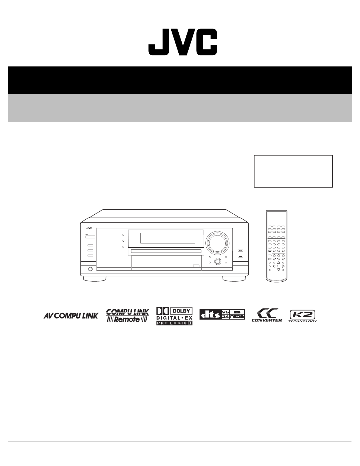
AUDIO/VIDEO CONTROL RECEIVER
2207120036
RX-8030VBK
Area suffix
J ----------------------------- U.S.A.
C -------------------------- Canada
A/V CONTROL RECEIVER
231
MENU
564
ENTER
7/P
89
+10
10/0
0
TABLE OF CONTENTS
1 Precautions . . . . . . . . . . . . . . . . . . . . . . . . . . . . . . . . . . . . . . . . . . . . . . . . . . . . . . . . . . . . . . . . . . . . . . . . . . 1-4
2 Disassembly method . . . . . . . . . . . . . . . . . . . . . . . . . . . . . . . . . . . . . . . . . . . . . . . . . . . . . . . . . . . . . . . . . . 1-6
3 Adjustment. . . . . . . . . . . . . . . . . . . . . . . . . . . . . . . . . . . . . . . . . . . . . . . . . . . . . . . . . . . . . . . . . . . . . . . . . . 1-14
4 Description of major ICs. . . . . . . . . . . . . . . . . . . . . . . . . . . . . . . . . . . . . . . . . . . . . . . . . . . . . . . . . . . . . . . 1-16
COPYRIGHT © 2003 VICTOR COMPANY OF JAPAN, LIMITED
No.22071
2003/6
Page 2
Amplifier Output Power
Audio Input Sensitivity/Impedance
(1 kHz)
Audio Input (DIGITAL IN)*
Audio Output Level PRE OUT : 1 V
Recording Output Level VCR 1 OUT, VCR 2 OUT, CDR OUT, TAPE/MD OUT : 200 mV
Digital output Optical : DIGITAL OUTPUT
Signal wave length 660 nm
Audio
Output level -21 dBm to -15 dBm
Signal-to-Noise Ratio ('66 IHF/'78 IHF)
PHONO IN 70 dB/78 dB (at REC OUT)
DVD IN, VCR 1 IN, VCR 2 IN, TV
SOUND/DBS IN, VIDEO
CD IN, CDR IN, TAPE/MD IN 87 dB/80 dB
Frequency Response (8Ω)
SPECIFICATION
130 W per channel, min. RMS, driven into
At Stereo operation Front ch
Front ch
Center ch
At Surround
operation
Surround ch
Surround Back ch
PHONO IN (MM) 2.5 mV/47 kΩ
DVD IN, VCR 1 IN, VCR 2 IN, TV
SOUND/DBS IN, VIDEO IN
CD IN, CDR IN, TAPE/MD IN 200 mV/47 kΩ
Coaxial DIGITAL 1 (DVD) : 0.5 V(p-p)/75 Ω
Optical
87 dB/80 dB
PHONO IN 20 Hz to 20 kHz (±1 dB)
DVD IN, VCR 1 IN, VCR 2 IN, TV
SOUND/DBS IN, VIDEO
CD IN, CDR IN, TAPE/MD IN 20 Hz to 100 kHz (+1 dB, -3 dB)
RIAA Phono Equalization ±1.0 dB (20 Hz to 20 kHz)
Equalization (5 bands) 63 Hz, 250 Hz, 1 kHz, 4 kHz, 16 kHz (±8 dB)
Bass boost +6 dB ±1.0 dB at 100 Hz
DIGITAL 2 (CD), DIGITAL 3 (TV), DIGITAL 4 (CDR) :
-21 dBm to -15 dBm (660 nm ±30 nm)
8Ω, 20 Hz to 20 kHz, with no more than
0.08% total harmonic distortion.
130 W per channel, min. RMS, driven into
8Ω at 1 kHz, with no more than 0.8% total
harmonic distortion.
130 W, min. RMS, driven into 8Ω at 1 kHz,
with no more than 0.8% total harmonic
distortion.
130 W per channel, min. RMS, driven into
8Ω at 1 kHz, with no more than 0.8% total
harmonic distortion.
130 W, min. RMS, driven into 8Ω at 1 kHz,
with no more than 0.8% total harmonic
distortion.
200 mV/47 kΩ
20 Hz to 100 kHz (+1 dB, -3 dB)
1-2 (No.22071)
Page 3
Composite video
Video Input Sensitivity/Impedance
Video
Video Output Level
Tuning Range 87.5 MHz to 108.0 MHz
FM tuner
(IHF)
AM tuner Tuning Range 530 kHz to 1 710 kHz
General
* Corresponding to Linear PCM, Dolby Digital, and DTS Digital Surround (with sampling frequency - 32 kHz, 44.1 kHz, 48 kHz).
Designs & specifications are subject to change without notice
Usable Sensitivity Monaural 12.8 dBf (1.2 µV/75 Ω)
50 dB Quieting Sensitivity Monaural 16.0 dBf (1.7 µV/75 Ω)
Stereo 37.5 dBf (20.5 µV/75 Ω)
Stereo Separation at REC OUT 35 dB at 1 kHz
Power Requirements AC 120V~, 60 Hz
Power Consumption 320 W/440 VA (at operation) 2 W (in standby mode)
Dimensions (W × H × D) 435 mm × 157 mm × 425 mm (17 3/16 in. × 6 3/16 in. × 16 3/4 in.)
Mass 12.2 kg (27.0 lbs)
S-video
Component video
Composite video
S-video
Component video MONITOR OUT
Synchronization Negative
Signal-to-Noise Ratio 45 dB
DVD IN, VCR 1 IN, VCR 2 IN, TV
SOUND/DBS IN, VIDEO
(Y: luminance): 1 V(p-p)/75 Ω
(C: chrominance,
burst):
(Y: luminance): 1 V(p-p)/75 Ω
(PB/PR): 0.7 V(p-p)/75 Ω
VCR 1 OUT, VCR 2 OUT, MONITOR
OUT
VCR 1 OUT, VCR
2 OUT,
MONITOR OUT
(Y: luminance) 1 V(p-p)/75 Ω
(C: chrominance,
burst)
(Y: luminance) 1 V(p-p)/75 Ω
(PB/PR) 0.7 V(p-p)/75 Ω
1 V(p-p)/75 Ω
0.286 V(p-p)/75 Ω
1 V(p-p)/75 Ω
0.286 V(p-p)/75 Ω
(No.22071)1-3
Page 4
SECTION 1
Good earth ground
d
AC VOLTMETER
Precautions
1.1 Safety Precautions
(1) This design of this product contain s special hardware and
many circuits and components specially for safety purposes. For continued protection, no changes should be made
to the original design unless authorized in writing by the
manufacturer. Replacement parts must be identical to
those used in the original circuits. Services should be performed by qualified personnel only.
(2) Alterations o f the design or circuitry of the product sh ould
not be made. Any design alterations of the product should
not be made. Any design alterations or additions will void
the manufacturers warranty and will further relieve the
manufacture of responsibility for personal injury or property
damage resulting therefrom.
(3) Many electrical and mechanical parts in the products have
special safety-related characteristics. These characteristics are often not evident from visual inspection nor can the
protection afforded by them necessarily be obtained by using replacement components rated for higher voltage, wattage, etc. Replacement parts which have these special
safety characteristics are identified in the Parts List of Service Manual. Electrical components having such features
are identified by shading on the schematics and by ( ) on
the Parts List in the Service Manual. The use of a substitute
replacement which does not have the same safety characteristics as the recommended replacement parts shown in
the Parts List of Service Manual may create shock, fire, or
other hazards.
(4) The leads in the products are routed and dressed with ties,
clamps, tubings, barriers and the like to be separated from
live parts, high temperature parts, moving parts and/or
sharp edges for the prevention of electric shock and fire
hazard. When service is required, the origin al lead routing
and dress should be observed, and it should be confirmed
that they have been returned to normal, after reassembling.
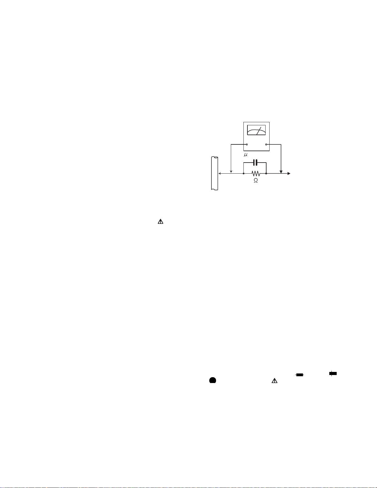
(5) Leakage shock hazard testing
After reassembling the product, always perform an isolation check on the exposed metal parts of the product (antenna terminals, knobs, metal cabinet, screw heads,
headphone jack, control shafts, etc.) to be sure the product
is safe to operate without danger of electrical shock.Do not
use a line isolation transformer during this check.
• Plug the AC line cord directly into the AC outlet. Using a
"Leakage Current Tester", measure the leakage current
from each exposed metal parts of the cabinet, particularly any exposed metal part having a return path to the
chassis, to a known good earth ground. Any leakage current must not exceed 0.5mA AC (r.m.s.).
• Alternate check method
Plug the AC line cord directly into the AC outlet. Use an
AC voltmeter having, 1,000Ω per volt or more sensitivity
in the following manner. Connect a 1,500Ω 10W resistor
paralleled by a 0.15µF AC-type capacitor between an exposed metal part and a known good earth ground.
Measure the AC voltage across the resistor with the AC
1-4 (No.22071)
voltmeter.
Move the resistor connection to each exposed metal
part, particularly any exposed metal part having a return
path to the chassis, and measure the AC voltage across
the resistor. Now, reverse the plug in the AC outlet and
repeat each measurement. Voltage measured any must
not exceed 0.75 V AC (r.m.s.). This corresponds to 0.5µ
mA AC (r.m.s.).
(Having 1000
ohms/volts,
or more sensitivity)
0.15 F AC TYPE
Place this
probe on
1500 10W
1.2 Warning
(1) This equipment has been designed and manufactured to
meet international safety standards.
(2) It is the legal respo nsibility of the repairer to ensure that
these safety standards are maintained.
(3) Repairs must be made in accordance with the relevant
safety standards.
(4) It is e ssential that safety critical components ar e replaced
by approved parts.
(5) If mains voltage selector is provided, check setting for local
voltage.
1.3 Caution Burrs formed during molding may be left over on some parts
of the chassis.
Therefore, pay attention to such burrs in the case of preforming repair of this system.
1.4 Critical parts for safety
In regard with component parts appearing on the silk-screen
printed side (parts side) of the PWB diagrams, the parts that are
printed over with black such as the resistor ( ), diode ( )
and ICP ( ) or identified by the " " mark nearby are critical
for safety. When replacing them, be sure to use the parts of the
same type and rating as specified by the manufacturer.
(This regulation dose not Except the J and C version)
each expose
metal part.
Page 5
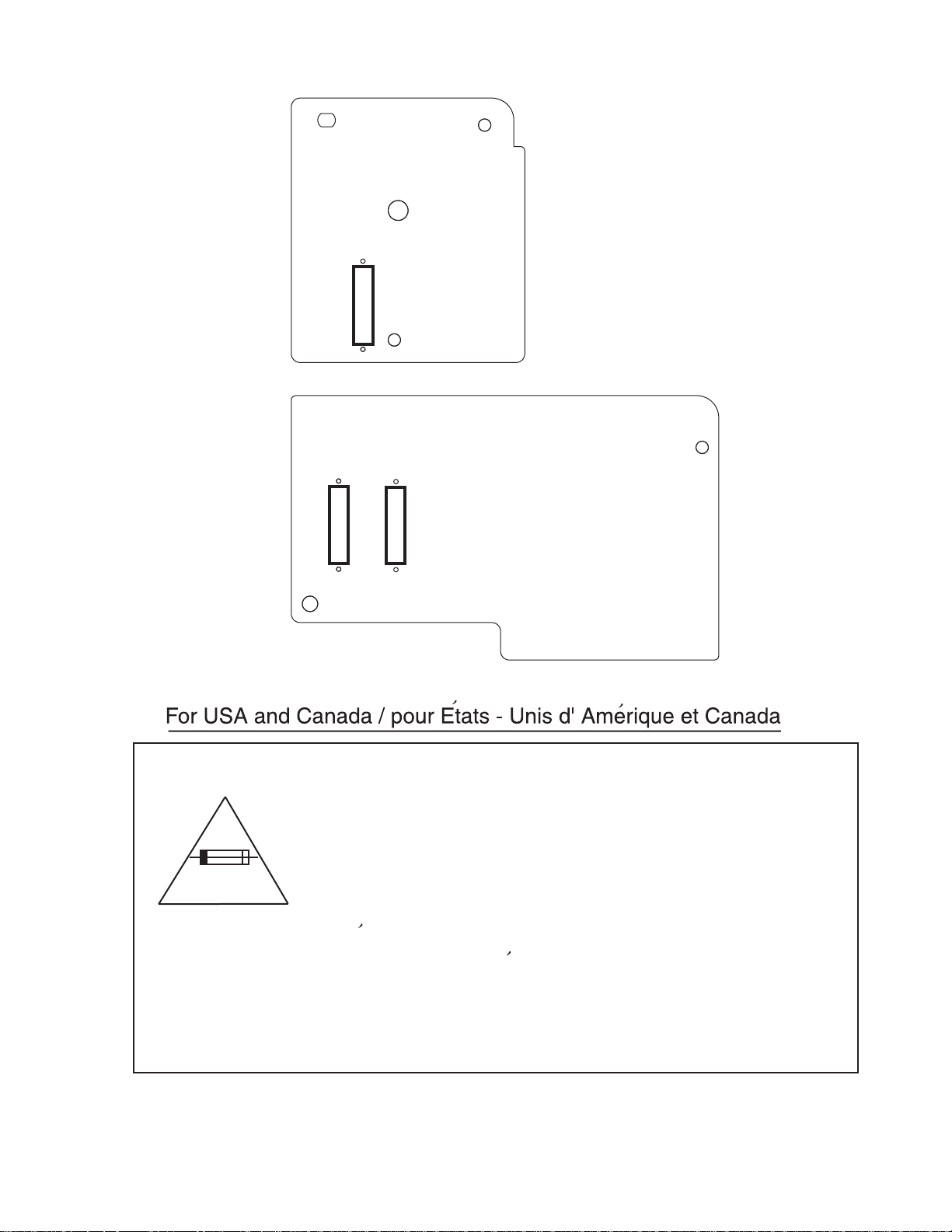
1.5 Importance administering poin on the safety
Primary part
F 1
6.3A-125V
Secondary parts
F 62
F 61
2A-125V
2A-125V
Caution: For continued protection against risk of
fire, replace only with same type 6.3A/125V for
F1, 2A/125V for F61 and F62.
This symbol specifies type of fast operating fuse.
Precaution: Pour eviter risques de feux, remplacez
le fusible de surete de F1 comme le meme type
que 6.3A/125V, et 2A/125V pour F61 et F62.
Ce sont des fusibles suretes qui functionnes rapide.
^
(No.22071)1-5
Page 6
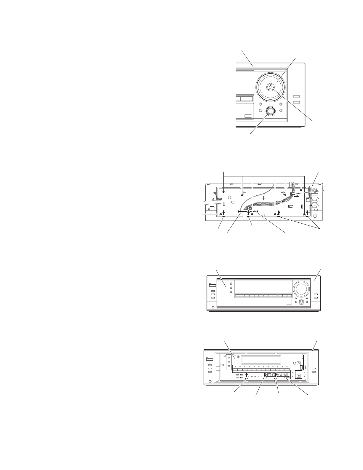
SECTION 2
f
1
Disassembly method
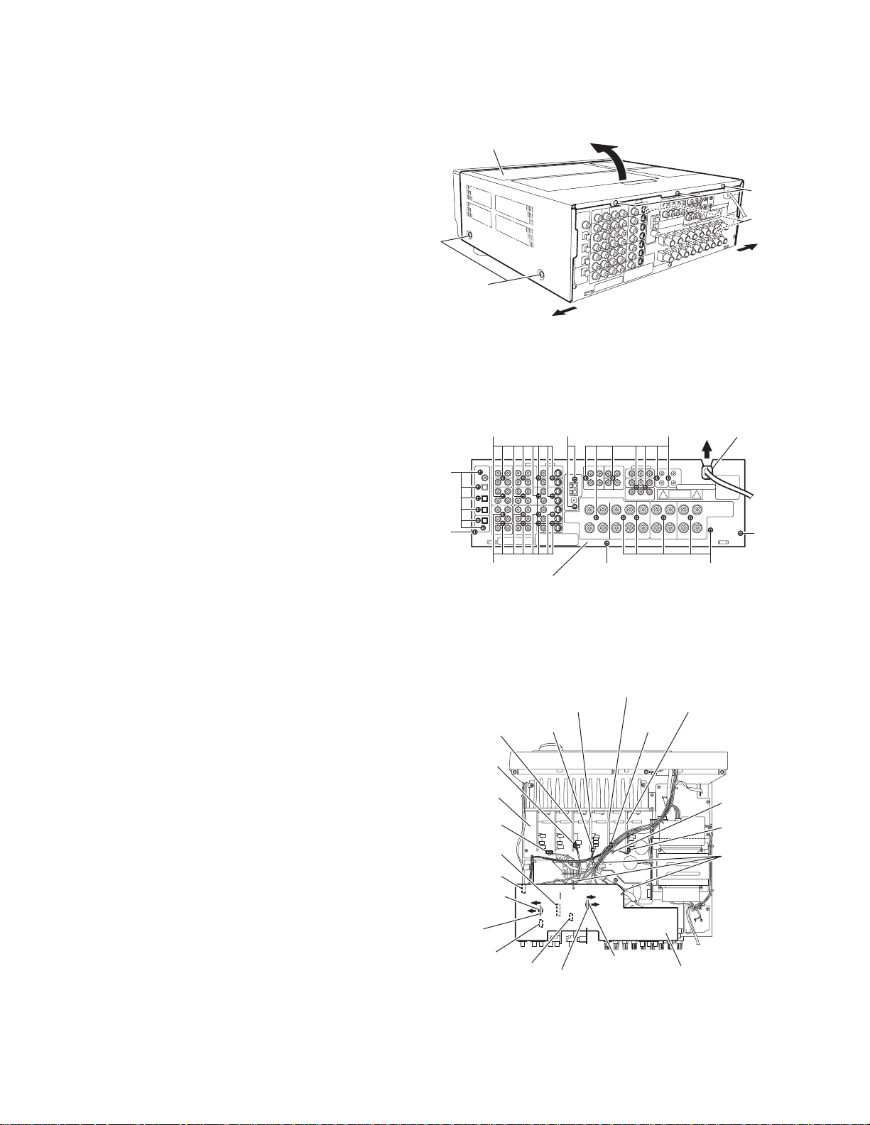
2.1 Removing the top cover (See Fig.1)
(1) From the right and left sides of th e main body, remove the
four screws A attaching the top cover.
(2) From the back side of the main body, remove the three
screws B attaching the top cover.
(3) Remov e the to p cover in the di recti on of th e arrow 2 w hile
extending the lower sections of the top cover in the direction of the arrow 1.
2.2 Removing the rear panel (See Fig.2)
• Prior to performing the following procedures, remove the top
cover.
(1) From the back side of the main body, remove the strain re-
lief from the rear panel in the direction of the arrow.
(2) Remove the thirty-four screws C, two screws D and three
screws E attaching the rear panel.
Top cover
C
E
A
C
2
B
A
1
1
Fig.1
D
C
Strain relie
E
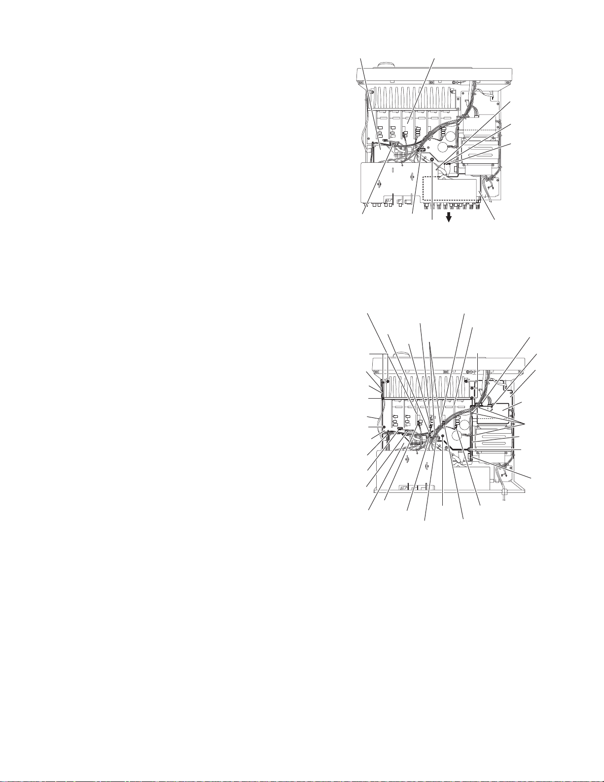
2.3 Removing the I/O board (See Fig.3)
• Prior to performing the following procedures, remove the top
cover and rear panel.
(1) From the top side of the main body, remove the two plastic
rivets in the direction of the arrow 1.and remove the stopper boards in the direction of the arrow 2.
(2) Remove the tie bands bundling the wires.
(3) Disconnect the wire from the connector CN722 on the cen-
ter board.
(4) Disconnect the wire from the connector CN714 on the front
board (L).
(5) Disconnect the wire from the connector CN717 on the sur-
round back board.
(6) Disconnect the wire from the connector CN719 on the front
board (R).
Disconnect the wire from the connector CN723 on the main
board.
(7) Disconnect the connectors (CN205, CN361, CN381,
CN501) on the I/O board in an upward direction.
Front board(R)
CN719
Main board
CN723
CN381
CN501
Plastic rivet
Stopper board
CN361
CN205
Rear panel
Surround board
CN717 CN714
2
2
1
1
Stopper board
EC
Fig.2
Front board(L)
2
2
1
1
Plastic rivet
Fig.3
C
Center board
Tie band
CN722
Tie bands
I/O board
1-6 (No.22071)
Page 7
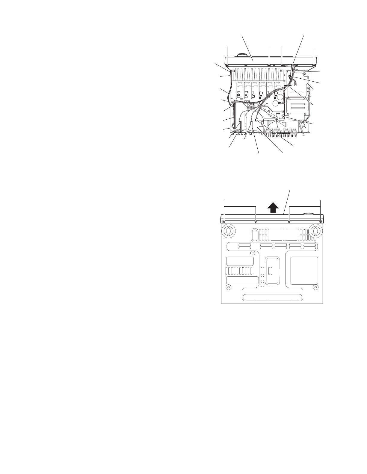
2.4 Removing the front panel assembly (See Fig.4 and Fig.5)
• Prior to performing the following procedures, remove the top
cover, rear panel and I/O board.
(1) From the top side of the main bod y, remove the tie bands
bundling the wires. (See Fig.4)
(2) Disconnect the wire from the connector CN599 on the DSP
board. (See Fig.4)
(3) Disconnect the wire from the connector CN415 on the
Audio2 board. (See Fig.4)
(4) Disconnect the wire from the connector CN206 on the Vid-
eo board. (See Fig.4)
(5) Disconnect th e wire from the connector CN244 on the S-
Video board. (See Fig.4)
(6) Disconnect the card wire from connector CN402 on the
power supply board. (See Fig.4)
(7) Disconnect the card wire from connector CN400 on the mi-
con board. (See Fig.4)
(8) Remove the tie band and wire protection board fixing the
card wire. (See Fig.4)
(9) Remove the three screws F and screw G attaching the front
panel assembly. (See Fig.4)
REFERENCE :
When attaching the screw G, attach the earth wire with it.
(10) From the bottom side of the main body, remove the four
screws H attaching the front panel assembly. (See Fig.5)
(11) Remove the front panel assembly in the direction of the ar-
row. (See Fig.5)
Wire
protection
board
Tie band
Card wire
Tie band
CN400
DSP board
CN599
CN415
Audio2 board
Front panel assembly
F
CN206
Video board
FFG
Fig.4
Front panel assembly
Card wire
Tie band
CN402
Power supply
board
Tie band
Micon board
CN244
S-Video board
HH
Fig.5
(No.22071)1-7
Page 8
2.5 Removing the tuner, DSP board, Audio board, Audio2 board, Video board and S-Video board (See Fig.6)
• Prior to performing the following procedures, remove the top
cover, rear panel and I/O board.
(1) From the top side of the main body, remove the tie band
bundling the wire.
(2) Disconnect the card wire from connector CN314 on the Au-
dio board, and take out the tuner.
(3) Disconnect the wire from the connector CN599 on the DSP
board.
(4) Disconnect the DSP board from the connector CN601 on
the micon board.
(5) Disconnect the wire from the connector CN415 on the
Audio2 board.
(6) Disconnect the Audio2 board from the connector CN301 on
the micon board.
(7) Disconnect the Audio board from the connectors (CN101,
CN303) on the micon board.
(8) Disconnect the wire from the connector CN206 on the Vid-
eo board.
(9) Disconnect the Video board from the connector CN201 on
the micon board.
(10) Di sconnect the wire from the connector CN244 on the S-
Video board.
(11) Di sconnect the S-Video board from the connector CN241
on the micon board.
CN314
Tie band
CN303
CN101
CN415
DSP board
CN601
CN599
CN301
Audio2 board
Card wire
Video board
Audio board
CN206
S-video board
Fig.6
CN201
CN244
Tuner
Micon board
CN241
2.6 Removing the micon board (See Fig.7)
• Prior to performing the following procedures, remove the top
cover, rear panel, I/O board, tuner, DSP board, Audio board,
Audio2 board, Video board and S-Video board.
(1) From the top sid e of the main body, disconnect the card
wire from the connector CN400 on the micon board.
(2) Disconne ct the relay board from the connector CN81 on
the micon board.
(3) Disconne ct the parallel wire from the connectors CN931
and CN932 on the micon board.
(4) Disconne ct the paral lel wire from the conn ector CN83 1 on
the main board.
(5) Remove the two screws J and screw J' attaching the micon
board.
REFERENCE :
When attaching the screw J', attach the earth wire with it.
(6) Remove the three screws K attaching the transistors
(Q921, Q931, Q941) to the chassis base.
(7) Loosen the screw L attaching the micon board.
Card wire
J
CN400
J
Micon board
Transistors
(Q921,Q931,Q941)
K
CN831
CN931
J
Fig.7
Main board
Relay board
L
Chassis base
CN81
CN932
1-8 (No.22071)
Page 9
2.7 Removing the speaker board
r
(See Fig.8)
• Prior to performing the following procedures, remove the top
cover, rear panel.
(1) From the top side of the main body, remove the tie band
bundling the wires.
(2) Disconnect the wires from the connectors (CN813, CN814)
on the main board.
(3) Disconnect the parallel wire fro m the connectors (CN931,
CN932) on the micon board.
(4) Remove the screw J' attaching the micon board.
(5) Take out the speaker board in the direction of the arrow.
Micon board
Main board
Tie band
CN931
CN932
2.8 Removing the main board (See Fig.9)
• Prior to performing the following procedures, remove the top
cover.
(1) From the top side of the main bod y, remove the tie bands
bundling the card wire and wires.
(2) Remove the tie band and wire protection board bundling
the card wire.
(3) Disconnect the wire from the connector CN811 on the pow-
er transformer board 1.
(4) Disconnect the relay board from the connector (CN71,
CN81) on the power supply board and micon board.
(5) Disconnect the parallel wire fro m the connectors (CN831,
CN881) on the main board.
(6) Disconnect the wire from the connectors (CN72 3, CN813,
CN814) on the main board.
(7) Disconnect the wire from the connector CN722 on the cen-
ter board.
(8) Disconnect the wire from the connector CN714 on the front
board (L).
(9) Disconnect the wire from the connector CN717 on the sur-
round back board.
(10) Disconnect the wire from the connector CN719 on the front
board (R).
(11) Remove the screw L, six screws M and two screws N at-
taching the main board.
(12) Take out the main board.
CN814
Front board(R)
M
Tie band
Wire
protection
board
M
Card wire
N
Main board
Tie band
CN723
CN814
Micon board
CN813
Surround board
CN881
CN717
CN719
CN831
CN813
J
Fig.8
Front board(L)
Tie band
N
CN714
Fig.9
Speaker board
Center board
M
CN722
CN71
CN811
Power
supply
board
Power
transforme
board 1
Tie bands
Relay board
L
CN81
(No.22071)1-9
Page 10
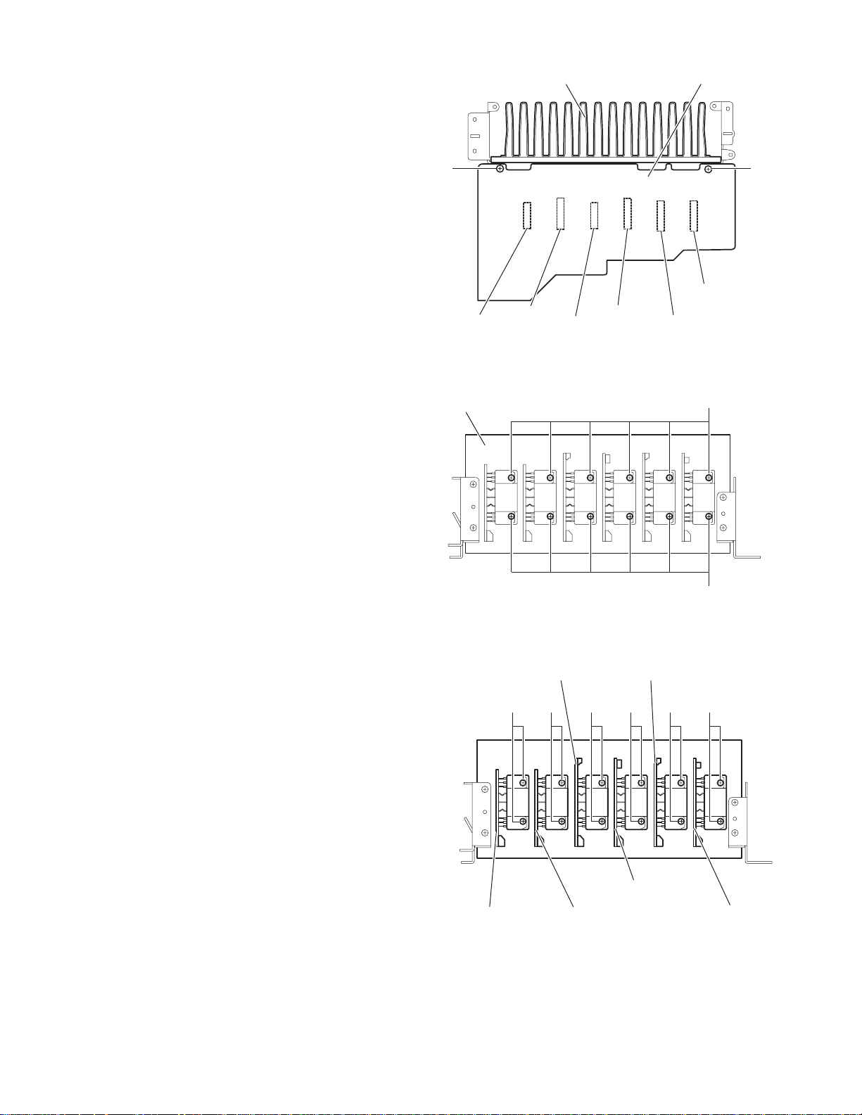
2.9 Removing the heat sink (See Fig.10 and 11)
• Prior to performing the following procedures, remove the top
cover and main board.
(1) From the reverse side of the main board , remove the two
screws P attaching the main board to the heat sink. (See
Fig.10)
(2) Disconnect the connector (CN701-CN706) on the main
board, remove the main board. (See Fig.10)
(3) Remove the twelve screws Q attaching the heat sink. (See
Fig.11)
2.10 Removing the center board, front boards (L/R), surround boards (L/R) and surround back board (See Fig.10 and Fig.12)
• Prior to performing the following procedures, remove the top
cover and main board.
(1) From the reverse side of the main board , remove the two
screws P attaching the main board to the heat sink. (See
Fig.10)
(2) Disconnect the connectors (CN701-CN706) on the main
board, remove the main board. (See Fig.10)
(3) Remove the two screws Q attaching the center board. (See
Fig.12)
(4) Remove the two screws Q attaching the front board (L).
(See Fig.12)
(5) emove the two screws Q attaching the surround back
board. (See Fig.12)
(6) Remov e the two screws Q attaching the front board (R).
(See Fig.12)
(7) Remov e the two screws Q attaching the surround board
(L). (See Fig.12)
(8) Remov e the two screws Q attaching the surround board
(R). (See Fig.12)
P
CN703
Heat sink
Heat sink
CN701
CN704
CN702
Fig.10
Fig.11
Main board
P
CN706
CN705
Q
Q
Front board(R)
Q Q Q Q Q Q
Surround board(R)
Front board(L)
Surround back board
Surround board(L)
Fig.12
Center board
1-10 (No.22071)
Page 11
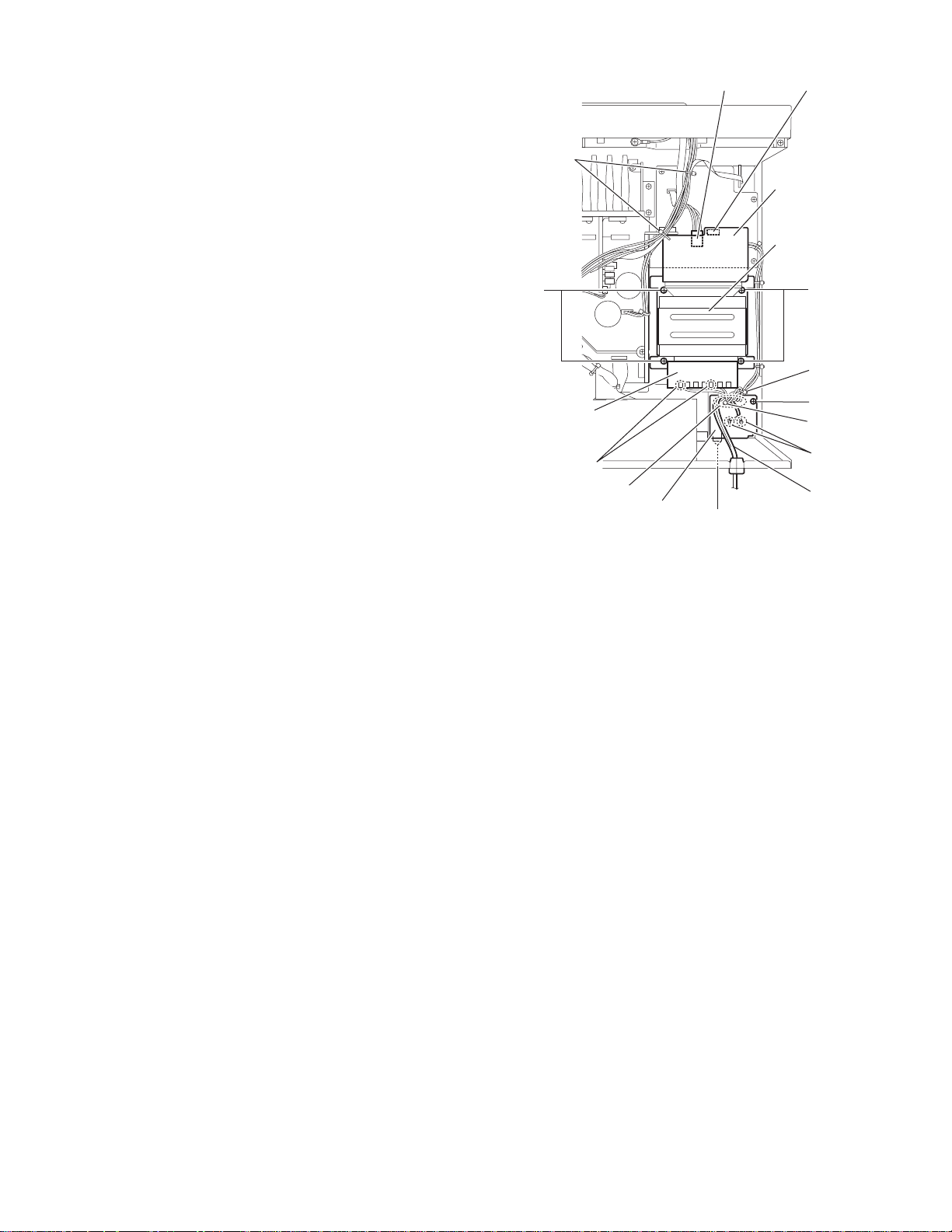
2.11 Removing the power transformer
r
r
(See Fig.13)
• Prior to performing the following procedures, remove the top
cover.
(1) From the top side of the main body, remove the tie band
bundling the wires.
(2) Disconnect the wire from the connectors (CN5 5, CN811)
on the power transformer board 1.
(3) Remove the solders from the solder ed sections a on the
power transformer board 2.
(4) Remove the four screws R attaching the powe r tra nsfor m-
er.
2.12 Removing the power/fuse board
(See Fig.13)
• Prior to performing the following procedures, remove the top
cover.
(1) From the back side and top side of the main body, remove
the tie band from the bundling the wires and the power
cord.
(2) Remove the screws S and scre w T attaching the power/
fuse board.
(3) Remove the solders from the soldered sections b attaching
the power cord.
(4) From the reverse side of the power/fuse board, remove the
solders from the soldered sections c attaching the wires.
Tie band
Power transformer
board 2
Soldered
sections a
Soldered
sections c
Power/fuse
board
Fig.13
CN811
S
CN55
Power transforme
board 1
Power transforme
RR
Tie band
T
Tie band
Soldered
sections b
Power cord
(No.22071)1-11
Page 12
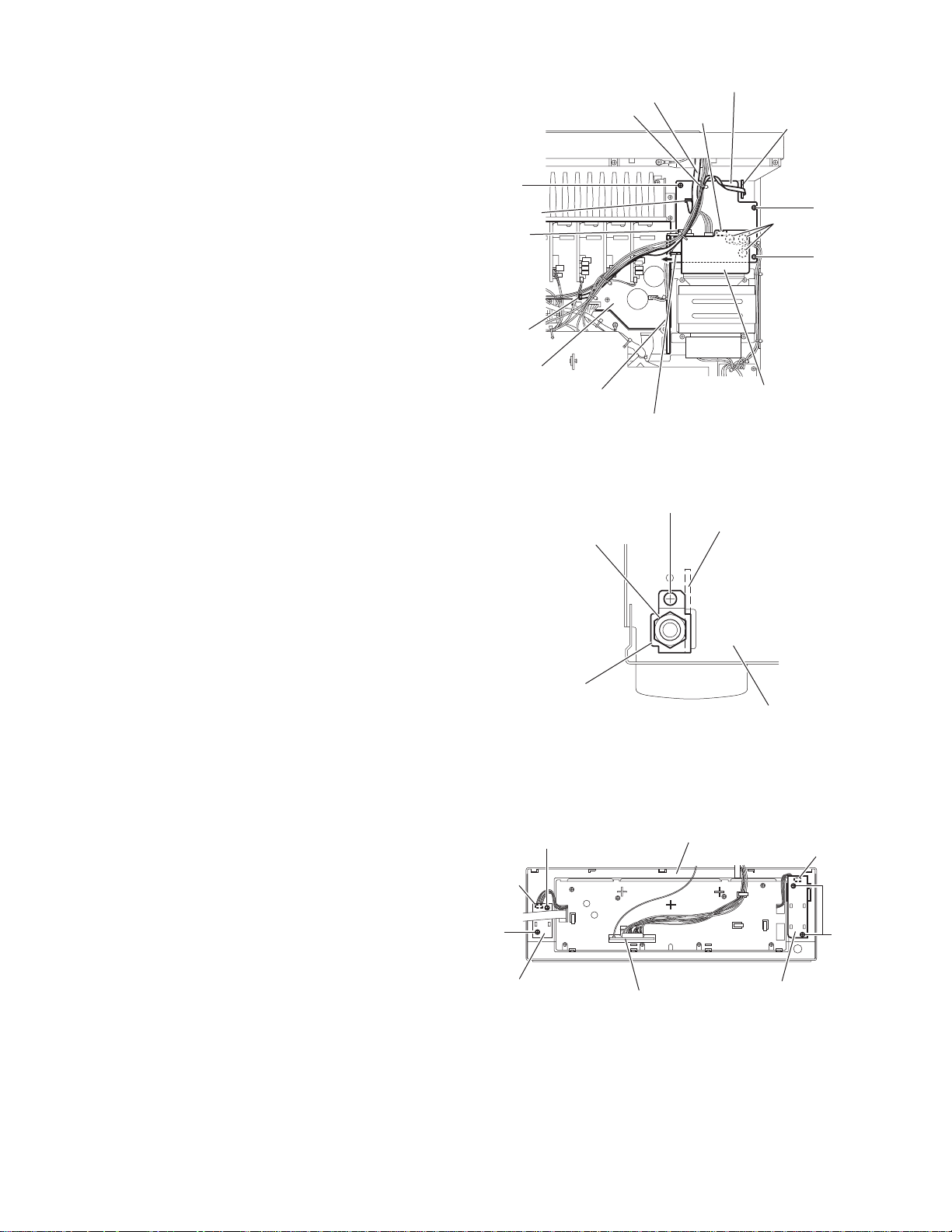
2.13 Removing the power surly board
r
(See Fig.14)
• Prior to performing the following procedures, remove the top
cover.
(1) From the top side of the main body, disconnect the parallel
wire from the connector CN55 on the power transformer
board 1.
(2) Disconnect the card wire from the connector CN402 on the
power supply board.
(3) Disconne ct the relay board from the connector CN71 on
the power supply board.
(4) Remove the three screws U attaching the power supply
board.
(5) Remo ve the power supply board from the hook d of the
chassis base bracket in the direction of the arrow, and take
out the power supply board.
(6) Turn over the power supply board, and remove the solders
from the soldered sections e attaching the wire.
2.14 Removing the headphone jack board
(See Fig.14 and Fig.15)
• Prior to performing the following procedures, remove the top
cover, rear panel, I/O board and front panel assembly.
(1) From the top side of the main body, disconnect the parallel
wire from the connector CN881 on the main board. (See
Fig.14)
(2) From the fro nt side of the main body, remove the nut and
screw V attaching the headphone bracket to the front
bracket. (See Fig.15)
(3) Remove the three screws U attaching the power supply
board. (See Fig.14)
(4) Take out the headphone jack board from the inside of the
chassis base while lifting the power supply board.
U
CN402
CN71
CN881
Main board
Main board
Tie band
Relay board
Hook (d) of the chassis
base bracket
Nut
Card wire
Fig.14
V
Power supply board
CN55
Headphone jack board
Headphone
jack board
Soldered
sections e
Power transforme
board 1
U
U
2.15 Removing the switch board
(See Fig.16)
• Prior to performing the following procedures, remove the top
cover, rear panel, I/O board and front panel assembly.
(1) From the back side of the front panel assembly, remove the
two screws W attaching the switch board.
(2) Take out the switch board, disco nnect the wire from the
connector CN432 on the switch board.
2.16 Removing the power switch board
(See Fig.16)
• Prior to performing the following procedures, remove the top
cover, rear panel, I/O board and front panel assembly.
(1) From the back side of the front panel assembly, remove the
two screws X attaching the power switch board.
(2) Take out the power switch board, disconnect the wire from
the connector CN430 on the power switch board.
Headphone bracket
W
CN432
W
Switch board
Fig.15
Front panel assembly
Front video board
Fig.16
Front bracket
CN430
X
Power switch board
1-12 (No.22071)
Page 13
2.17 Removing the front key & system control board, front video board
Y
(See Fig.17 to Fig.20)
• Prior to performing the following procedures, remove the top
cover, rear panel, I/O board, front panel assembly, switch
board and power switch board.
(1) From the front side of the front panel assembly, pull out the
volume and jog knobs, and remove the nut attaching the
front key & system control board. (See Fig.117)
(2) From the back side of the front panel assembly, remove the
eight screws Y attaching the sub panel assembly. (See
Fig.18)
(3) Remove th e wires of the front video board from the ho ok f
of the front panel assembly in the direction of the arrow 1.
(See Fig.18)
(4) Remove the sub panel assembly while releasing the claws
g in the direction of the arrow 2. (See Fig.18 and Fig.19)
(5) From the front side of the front panel assembly, disconnect
the wire from the connector CN412 on the front key & system control board, and take out the front video board. (See
Fig.20)
(6) Remove the claws h attaching the front key & system con-
trol board in the direction of the arrow and take out the front
key & system control board. (See Fig.20)
Front panel assembly
Jog knob
Y
Volume knob
Nut
Fig.17
Front panel assembly
1
2
2
Claws g Claws g Claws g
Front video board
Sub panel assembly
Front key & System control board
2
Sub panel assembly
Fig.18
Fig.19
Front panel assembly
2
Front panel assembly
Hook f
CN412
Claws hClaws h
Fig.20
Front video board
(No.22071)1-13
Page 14
SECTION 3
Adjustment
3.1 Adjustment method Tuner section
1. Tuner range
FM 87.5MHz to 108.0MHz
AM 530kHz to 1710kHz
Power amplifier section
Adjustment of idling current
Measurement location B2204-B2205 (Lch), B2213-B2214 (Rch)
Adjustment part VR787 (Lch), VR788 (Rch)
Attention:
This adjustment does not obtain a correct adju stment value i mmediately after the amplifier is used (state that an in ternal temperature has risen). Please adjust immediately after using the amplifier after turning off the power supply of
the amplifier and falling an internal temperature.
<Adjustment method>
(1) Set the vo lume control to minimum during this adjustment. (No signal & No load)
(2) Set the surround mode OFF.
(3) Turn VR787 and VR788 fully counterclockwise to warm up before adjustment.
If the heat sink is already warm from previous use the correct adjustment can not be made.
(4) For L-ch, connect a DC voltmeter between B2204 and B2205 (Lch) and, connect it between B2213 and B2214 (Rch).
(5) 30 minutes later after power on, adjust VR787 for Lch, or VR788 for Rch so that the DC voltmeter value has 1mV to 10mV.
• It is not abnormal though the idling current might not b ecome 0mA even if it is fin ished to turn variable re sistance (VR787,
VR788) in the direction of counterclockwise.
Front board (L)
VR787
B2204
B2205
Front board (R)
VR788
B2213
B2214
VR787 (Lch)
B2204, B2205 (Lch)
VR788 (Rch)
B2213, B2214 (Rch)
1-14 (No.22071)
Page 15

3.2 Self-diagnose function
This model incorporates the following self-diagnostic functions.
1. PROTECTOR
• The PROTECTOR IN port detects errors such as speaker overcurrent and DC voltage output errors (Active: L). Immediately after
detection, all relays are switched off and the alarm display as shown below (blinking at intervals of 0.5 sec. ON and 0.5 sec. OFF)
is displayed in the lower part of the FL matrix.
During the alarm display, all other FL and LED segments are turned off.
OVERLOAD
• The overload status can be canceled by switching the power off. When the power is switched on again, the unit is turned on in
the same abnormal status as before. Lower the volume level for 10 steps for protection. (If the previous volume level was between 0 and 9, lower it to 0).
• The detection by the protector is not performed for 4 seconds after power on.
2. Supply voltage error detection
• When the power is switched on, the supply voltage at the A/D input port (pins 2 to 5 and 7) is monitored and, when an error is
detected continuously for 1 second, the unit immediately enters the standby mode.
• When the power is switched on again, the unit is turned on in the same abnormal status as before.
• The supply voltage error detection is not performed for 4 seconds after power on.
• The following table shows the error detection thresholds.
At abnormal state (Low voltage) At normal state At abnormal state (High voltage)
Pin 2
Pin 3
Pin 4
Pin 5
Pin 7
Analog value : 0 - 2.2
Digital value : 000 - 1C0
Analog value : 0 - 2.2
Digital value : 000 - 1C0
Analog value : 0 - 2.2
Digital value : 000 - 1C0
Analog value : 0 - 2.2
Digital value : 000 - 1C0
Analog value : 0 - 2.2
Digital value : 000 - 1C0
Analog value : 2.2 - 2.8
Digital value : 1C1 - 240
Analog value : 2.2 - 2.8
Digital value : 1C1 - 240
Analog value : 2.2 - 2.8
Digital value : 1C1 - 240
Analog value : 2.2 - 2.8
Digital value : 1C1 - 240
Analog value : 2.2 - 2.8
Digital value : 1C1 - 240
Analog value : 2.8 - 5.0
Digital value : 241 - 3FF
Analog value : 2.8 - 5.0
Digital value : 241 - 3FF
Analog value : 2.8 - 5.0
Digital value : 241 - 3FF
Analog value : 2.8 - 5.0
Digital value : 241 - 3FF
Analog value : 2.8 - 5.0
Digital value : 241 - 3FF
(No.22071)1-15
Page 16

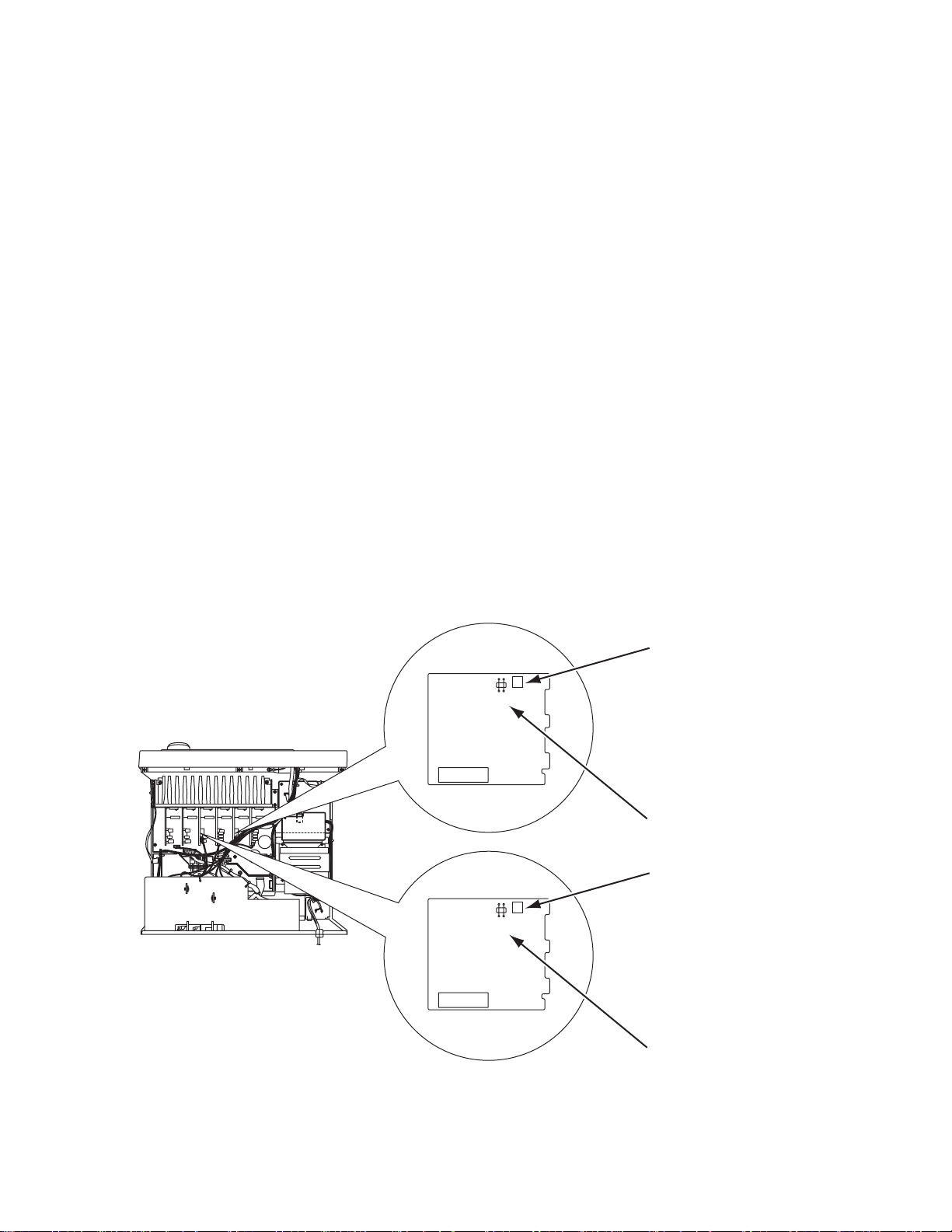
Description of major ICs
4.1 AK4112BVF-X (IC551) : Digital audio receiver
• Pin layout
SECTION 4
DVDD
DVSS
TVDD
V/TX
XTI
XTO
PDN
AVDD
AVSS
RX1
RX2/DIF0
RX3/DIF1
RX4/DIF2
1
2
3
4
5
6
7
8
R
9
10
11
12
13
14
CM0/CDTO
28
CM1/CDT1
27
OCKS1/CCLK
26
OCKS0/CSN
25
MCKO1
24
MCKO2
23
DAUX
22
BICK
21
SDTO
20
LRCK
19
ERF
18
FS96
17
P/SN
16
AUTO
15
• Pin function
Pin No. Symbol I/O Function
1 DVDD - Digital Power Supply Pin 3.3V
2 DVSS - Digital Ground Pin
3 TVDD - Input Buffer Power Supply Pin 3.3V
or 5V
4 V O Validity Flag Output Pin in Parallel
Mode
TX O Transmit channel (through data) Out-
put Pin in Serial Mode
5 XTI I X 'tal Input Pin
6 XTO O X'tal Output Pin
7 PDN I Power-Down Mode Pin
When "L" the AK4112B is powered-
down and reset
8 R - External Resistor Pin
18kohm +/-1% resistor to AVSS ex-
ternally.
9 AVDD - Analog Power Supply Pin
10 AVSS - Analog Ground Pin
11 RX1 I Receiver Channel 1
This channel is selected in Parallel
Mode or default of Serial Mode.
12 RX2 I Receiver Channel 2 in Serial Mode
12 DIF0 I Audio Data Interface Format 0 Pin in
Parallel Mode
13 RX3 I Receiver Channel 3 in Serial Mode
13 DIF1 I Audio Data Interface Format 1 Pin in
Parallel Mode
14 RX4 I Receiver Channel 4 in Serial Mode
14 DIF2 I Audio Data Interface Format 2 Pin in
Parallel Mode
15 AUTO O Non-PCM Detect Pin
"L": No detect "H": Detect
16 P/S I Parallel/Serial Select Pin
"L": Serial Mode "H": Parallel Mode
Pin No. Symbol I/O Function
17 FS96 O 96kHz Sampling Detect Pin (RX
Mode)
"H": fs=88.2kHz or more "L":
fs=54kHz or less.
(X'tal Mode) "H": XFS96=1 "L":
XFS96=0.
18 ERF O Unlock & Parity Error Output Pin
"L": No Error "H": Error
19 LRCK I/O Output Channel Clock Pin
20 SDTO O Audio Serial Data Output Pin
21 BICK I/O Audio Serial Data Clock Pin
22 DAUX I Auxiliary Audio Data Input Pin
23 MCK02 O Master Clock #2 Output Pin
24 MCK01 O Master Clock #1 Output Pin
25 OCKS0I O utput Clock Select 0 Pin in Parallel
Mode
CSN I Chip Select Pin in Serial Mode
26 OCKS1I O utput Clock Select 1 Pin in Parallel
Mode
CCLK I Control Data Clock Pin in Serial
Mode
27 CM1 I Master Clock Operation Mode Pin0 in
Parallel Mode
CDTI I Control Data Input Pin in Serial Mode
28 CM0 I Master Clock Operation Mode Pin1 in
Parallel Mode
CDTO O Control Data Output Pin in Serial
Mode
NOTE:
All input pins except internal pull-down pins should not be
left floating.
1-16 (No.22071)
Page 17

• Block diagram
AVSS
AVDD R MCKO1 MCKO2 XTI XTO
RX1
RX2
RX3
RX4
V/TX
DVDD
DVSS
PDN
Input
Selector
System
Control
Clock
Recovery
DAIF
Decoder
AC-3/MPEG
Detect
AUTO ERF P/S="L"
Clock
Generator
DEM
Error
Detect
X'tal
Oscillator
Serial Control Mode
96kHz
Detect
Audio
I/F
p I/F
FS96
DAUX
LRCK
BICK
SDTO
TVDD
CSN
CCLK
CDTO
CDTI
RX1
V
DVDD
DVSS
OCKS0
OCKS1
CM0
CM1
PDN
System
Control
AVSS
AVDD R MCKO1 MCKO2 XTI XTO
Clock
Recovery
DAIF
Decoder
AC-3/MPEG
Detect
AUTO ERF P/S="H"
Clock
Generator
DEM
Error
Detect
Parallel Control Mode
X'tal
Oscillator
4
96kHz
Detect
Audio
I/F
FS96
DAUX
LRCK
BICK
SDTO
DIF0
DIF1
DIF2
TVDD
OCKS0
OCKS1
CM0
CM1
(No.22071)1-17
Page 18

4.2 AK4527BVQP (IC571): A/D, D/A converter
• Pin layout
4443424140393837363534
1
2
3
4
5
6
7
8
9
10
11
1213141516171819202122
Top View
• Pin function
No. Symbol I/O Function
1 SDOS I SDTO Source Select Pin (Note 1)
"L" : Internal ADC output "H" : DAUX input
2 OSKS I Control Mode Select Pin
"L" : 3-wire Serial "H" : I2C Bus
3 MIS - Soft Mute Pin (Note 1) Connect to GND
When this pin goes to "H" soft mute cycle is initialized.
When returning to "L" the output mute releases.
4 BICK I Audio Serial Data Clock Pin
5 LRCK I/O Input Channel Clock Pin
6 SDTI1 I DAC1 Audio Serial Data Input Pin
7 SDTI2 I DAC2 Audio Serial Data Input Pin
8 SDTI3 I DAC3 Audio Serial Data Input Pin
9 SDTO O Audio Serial Data Output Pin
10 D,AUX - Sub Audio Serial Data Input Pin Connect to GND
11 DFS - Double Speed Sampling Mode Pin (Note 1)
"L" : Normal Speed "H" : Double Speed
12 DEMI - Connect to GND
No internal bonding.
13 DEMO - Zero Input Detect Enable Pin Connect to GND
"L" : mode 7 (disable) at parallel mode
- zero detect mode is selectable by DZFM2-0 bits at serial mode.
- H : mode 0 (DZF is AND of all six channels)
14 MCKO - Output Buffer Power supply Pin 2.7V~5.5V
15 DVDD I Digital Power Supply Pin 4.5V~5.5V
16 DVSS - De-emphasis Pin 0V
17 PD
I Power-Down & Reset Pin
When "L" the AK4527B is powered-down and the control registers are reset to default state.
If the state of P/S or CAD0-1 changes then the AK4527B must be reset by PDN.
18 XTS - Test Pin Connect to GND
This pin should be connected to DVSS.
19 ICKS - Connect to GND No internal bonding.
20 ADIF - Analog Input Format Select Pin Digital Power Supply
H : Full-differential input "L" : Single-ended input
21 CAD1 - Chip Address 1 Pin Connect to GND
33
32
31
30
29
28
27
26
25
24
23
1-18 (No.22071)
Page 19

No. Symbol I/O Function
22 CAD0 O Chip Address 0 Pin Connect to GND
23 LOUT3 O DAC3 Lch Analog Output Pin
24 ROUT3 O DAC3 Rch Analog Output Pin
25 LOUT2 O DAC2 Lch Analog Output Pin
26 ROUT2 O DAC2 Rch Analog Output Pin
27 LOUT1 O DAC1 Lch Analog Output Pin
28 ROUT1 O DAC1 Rch Analog Output Pin
29 LIN- I Lch Analog Negative Input Pin
30 LIN+ I Lch Analog Positive Input Pin
31 RIN- I Rch Analog Negative Input Pin
32 RIN+ I Rch Analog Positive Input Pin
33 VREFL - Zero Input Detect 2 Pin (Note 2) Non Connect
When the input data of the group 1 follow total 8192LRCK cycles with "0" input data this pin
goes to "H".
OVF O Analog Input Overflow Detect Pin (Note 3)
This pin goes to "H" if the analog input of Lch or Rch is overflows.
34 VCOM O Common Voltage Output PinAVDD/2
Large external capacitor around 2.2uF is used to reduce power-supply noise.
35 VREFH - Po sitive Voltage Reference Input PinAVDD
36 AVDD - Analog Power Supply Pin4.5V~5.5V
37 AVSS - Analog Ground Pin0V
38 XTI - Zero Input Detect 1 Pin (Note 2) Non connect
When the input data of the group 1 follow total 8192 LRCK cycles with "0" input data this pin
goes to "H".
39 XTO I Master Clock Input Pin
40 P1S - Parallel / Serial Select Pin
"L" : Serial control mode "H" : Parallel control mode
41 CS
CSN I Chip select pin in 3-wire serial control mode
42 DIF1 I Audio Data Interface Format 1 Pin in parallel mode
SCL/CCLK I Control Data Clock Pin in serial control mode
43 LOOP0 I Loopback Mode 0 Pin in parallel control mode
SAD/CDTI I/O Control Data Input Pin in serial control mode
44 CDTD I Loopback Mode 1 Pin (Note 1)
Note:
(1) SDOS, SMUTE, DFS, and LOOP1 pins are ORed with regi ster data if P/S = "L".
(2) The gr oup 1 and 2 can be selected by DZFM2-0 bit if P/S = "L" and DZFME = "L".
(3) This pin becomes OVF pin if OVFE bit is set to "1" at serial control mode.
(4) All inp ut pins should not be left floating.
I Audio Data Interface Format 0 Pin in parallel mode
This pin should be connected to DVDD at I2C bus control mode
I2C = "L" : CCLK(3-wire Serial) I2C = "H" : SCL(I2CBus)
Enables digital loop-back from ADC to 3 DACs.
I2C = "L" : CDTI(3-wire Serial) I2C = "H" : SDA(I2CBus)
Enable all 3 DAC channels to be input from SDTII.
(No.22071)1-19
Page 20

4.3 39VF0207CWHR01 (IC511) : EEPROM
• Pin layout
• Block diagram
Memory Address
A11
A9
A8
A13
A14
A17
WE#
VDD
NC
A16
A15
A12
A7
A6
A5
A4
CE#
OE#
WE#
1
2
3
4
5
6
7
8
9
10
11
12
13
14
15
16
X-Decoder
Address Buffer & Latches
Control Logic
32
31
30
29
28
27
26
25
24
23
22
21
20
19
18
17
OE#
A10
CE#
DQ7
DQ6
DQ5
DQ4
DQ3
Vss
DQ2
DQ1
DQ0
A0
A1
A2
A3
EEPROM
Cell Array
Y-Decoder
I/O Buffers & Data Latches
DQ7~DQ0
• Pin function
Symbol Pin name Function
AMS- A0 Address Inputs To provide memory address. During Sector-Erase AMS-A12 address lines will select the
sector.
DQ7- DQ0 Data Input/Output To output data during read cycles and receive input data during write cycles. Data is in-
ternally latched during a write cycle. The outputs are in tri-state when OE# or CE# is
high.
CE# Chip Enable To active the device when CE# is low.
OE# Output Enable To gate the data output buffers.
WE# Write Enable To control the write operations.
VDD Power Supply To provide power supply voltage: 3.0-3.6V for SST39LF512/010/020/040
2.7-3.6V for SST39VF512/010/010/040
Vss Ground
NC No Connection Unconnected Pins
1-20 (No.22071)
Page 21

4.4 BA7625 (IC201/IC242) : Video selector
• Block diagram • Truth table
MONITOR OUT
GND
1
2
16
IN1
15
CTL A
A B E MONOTOR OUT
LL* IN1
HL* IN2
LH* IN3
IN5
GND
IN4
CTL E
IN3
CTL D
13
12
11
10
9
VOUT 1
CC
V
IN2
CTL B
VOUT 2
CTL C
3
4
5
6
7
8
logic
logic
HHL IN4
HHH IN5
CDE VOUT1
LL* -HL* IN2
LH* IN3
HHL IN4
HHH IN5
14
CDE VOUT2
LL* IN1
HL* -LH* IN3
HHL IN4
HHH IN5
4.5 BA7626 (IC241) : Video selector
• Block diagram • Truth table
MONITOR OUT
GND
1
2
16
IN1
15
CTL A
A B E MONOTOR OUT
LL* IN1
HL* IN2
LH* IN3
IN5
GND
IN4
CTL E
IN3
CTL D
13
12
11
10
9
VOUT 1
V
CC
IN2
CTL B
VOUT 2
CTL C
3
4
5
6
7
8
logic
logic
HHL IN4
HHH IN5
CDE VOUT1
LL* --
HL* IN2
LH* IN3
HHL IN4
HHH IN5
14
CDE VOUT2
LL* IN1
HL* --
LH* IN3
HHL IN4
HHH IN5
(No.22071)1-21
Page 22

4.6 DSPD56367PV150 (IC501) : DSP
• Pin layout
108 73
109 72
144 37
136
• Block diagram
1
TRIPLE
TIMER
2
DAX
(SPDIF Tx.)
INTER-FA
CE
ADDRESS
GENERATION
UNIT
SIX CHANNELS
DMA UNIT
INTERNAL
DATA
BUS
HOST
INTER-
FACE
16
8
ESAI
INTER-
FACE
ESAI_1
PERIPHERAL
EXPANSION AREA
PIO_EB
DSP56300
4
24-BIT
Core
6
SHI
INTER-
FACE
5
MEMORY EXPANSION AREA
PROGRAM
RAM
/INTERFACE
3K x 24
PROGRAM
ROM
40K x 24
Bootstrap
DDB
YDB
XDB
PDB
GDB
PM_EB
YAB
XAB
PAB
DAB
X MEMORY
RAM
13K x 24
ROM
32K x 24
XM_EB
Y MEMORY
RAM
7K x 24
ROM
8K x 24
YM_EB
EXTERNAL
ADDRESS
SRAM BUS
INTERFACE
I-CACHE
EXTERNAL
DATA BUS
BUS
SWITCH
DRAM &
&
SWITCH
18
ADDRESS
10
CONTROL
24
DATA
1-22 (No.22071)
PLL
CLOCK
GENERAT
EXTAL
RESET
PINIT/NMI
PROGRAM
INTERRUPT
CONTROLLER
PROGRAM
DECODE
CONTROLLER
MODA/IRQA
MODB/IRQB
MODC/IRQC
MODD/IRQD
PROGRAM
ADDRESS
GENERATOR
DATA ALU
+->
24X24 56 56-BIT MAC
TWO 56-BIT ACCUMULATORS
BARREL SHIFTER
24 BITS BUS
POWER
MNGMNT
JTAG
™
OnCE
4
Page 23

• Pin function
Pin No. Symbol I/O Function
1 SCK I/O SPI Serial Clock
2 SS I SPI Slave Select
3 HREQ I/O Host Request
4 SDO0 O Serial Data Output 0
5 SDO1 O Serial Data Output 1
6 SDO2 O Serial Data Output 2
6 SDI3 I Serial Data Input 3
7 SDO3 O Serial Data Output 3
7 SDI2 I Serial Data Input 2
8 VCCS - SHIESAIESAI_1DAX and Timer Power
9 GNDS - SHIESAIESAI_1DAX and Timer Ground
10 SDO4 O Serial Data Output 4
10 SDI1 I Serial Data Input 1
11 SDO5 O Serial Data Output 5
11 SDI0 I Serial Data Input 0
12 FST I/O Frame Sync for Transmitter
13 FSR I/O Frame Sync for Receiver
14 SCKT I/O Transmitter Serial Clock
15 SCKR I/O Receiver Serial Clock
16 HCKT I/O High Frequency Clock for Transmitter
17 HCKR I/O Hig h Frequency Clock for Receiver
18 VCCQL - Quiet Core (Low) po wer
19 GNDQ - Quiet Ground
20 VCCQH - Quiet External (High) Power
21 HDS I Host Data Strobe
21 HWR I Host Write Data
22 HRW I Host Read/Write
22 HRD I Host Read Data
23 HACK I Host Acknowledge
23 HRRQ O Receive Host Request
24 HOREQ O Host Request
24 HTRQ O Transmit Host Request
25 VCCS - SHIESAIESAI_1DAX and Timer Power
26 GNDS - SHIESAIESAI_1DAX and Timer Ground
27 ADO O Digital Audio Data Output
28 ACI I Audio Clock Input
29 TIO0 I/O Timer 0 Schmitt-Trigger Input/Output
30 HCS I Host Chip Select
31 HA2 I host Address In put 2
31 HA9 I Host Address 9
32 HA1 I Host Address Input 1
32 HA8 I Host Address 8
33 HA0 I Host Address Input 0
33 HAS I Host Address Strobe
34 to 37 HAD7 to HAD4 I/O Host Address/Data
(No.22071)1-23
Page 24

Pin No. Symbol I/O Function
38 VCCH - Host Power
39 GNDH - Host Ground
40 to 43 HAD3 to HAD0 I/O Host Address/Data
44 RESET I Reset
45 VCCP - PLL Power
46 PCAP I PLL Capacitor
47 GNDP - PLL Ground
48 SDO5_1 O Serial Data Output 5_1
48 SDI2_1 I Serial Data Input 2
49 VCCQH - Quiet External (High) Power
50 FST_1 I/O Frame Sync for Transmitter_1
51 AA2 O Address Attribute
51 RAS2 O Row Address Strobe
52 CAS O Column Address Strobe
53 SCKT_1 I/O Transmitter Serial Clock_1
54 GNDQ - Quiet Ground
55 EXTAL I External Clock Input
56 VCCQL - Quiet Core (Low) Power
57 VCCC - Bus Control Power
58 GNDC - Bus Control Ground
59 CLKOUT O Not connect
60 NC - Not connect
61 FSR_1 I/O Frame Sync for Rece iver_1
62 SCKR_1 I/O Receiver Serial Clock_1
63 BR O Bus Request
64 BB I/O Bus Busy
65 VCCC - Bus Control Power
66 GNDC - Bus Control Ground
67 WR O Write Enable
68 RD O Read Enable
69 AA1 O Address Attribute
69 RAS1 O Row Address Strobe
70 AA0 O Address Attribute
70 RAS0 O Row Address Strobe
71 BG I Bus Grant
72,73 A0,A1 O Address Bus
74 VCCA - Address Bus Power
75 GNDA - Address Bus Ground
76 to 79 A2 to A5 O Address Bus
80 VCCA - Address Bus Power
81 GNDA - Address Bus Ground
82 to 85 A6 to A9 O Address Bus
86 VCCA - Address Bus Power
87 GNDA - Address Bus Ground
88,89 A10,A11 O Address Bus
90 GNDQ - Quiet Ground
1-24 (No.22071)
Page 25

Pin No. Symbol I/O Function
91 VCCQL - Quiet Core (Low) Powe r
92 to 94 A12 to A14 O Address Bus
9 VCCQH - Quiet External (High) Power
96 GNDA - Address Bus Ground
97 to 99 A15 to A17 O Address Bus
100 to 102 D0 to D2 I/O Data Bus
103 VCCD - Data Bus Power
104 GNDD - Data Bus Ground
105 to 110 D3 to D8 I/O Data Bus
111 VCCD - Data Bus Power
112 GNDD - Data Bus Ground
113 to 118 D9 to D14 I/O Data Bus
119 VCCD - Data Bus Power
120 GNDD - Data Bus Ground
121 to 125 D15 to D19 I/O Data Bus
126 VCCQL - Quiet Core (Low) Power
127 GNDQ - Quiet Ground
128 D20 I/O Data Bus
129 VCCD - Data Bus Power
130 GNDD - Data Bus Ground
131 to 133 D21 to D23 I/O Data Bus
134 MODD I Mode Select D
134 IRQD I External Interrupt Request D
135 MODC I Mode Select C
135 IRQC I External Interrupt Request C
136 MODB I Mode Select B
136 IRQB I External Interrupt Request B
137 MODA I Mode Select A
137 IRQA I External Interrupt Request A
138 SDO4_1 O Serial Data Output 4_1
138 SDI1_1 I Serial Data Input 1_1
139 TDO O Test Data Output
140 TDI I Test Data Input
141 TCK I Test Clock
142 TMS I Test Mode Select
143 MOSI I/O SPI Master-Out-Slave-In
143 HA0 I IIC Slave Address 0
144 MISO I/O SPI Master-In-Slave-Out
144 SDA I/O IIC Data and Acknowledge
(No.22071)1-25
Page 26

4.7 GP1UM281X (IC404) : Dual operation amplifier
R
L
Amp
B.P.FLimiter
Demodulator
Integrator
Comparator
GND Vcc Vout
4.8 HA17558AF-X (IC303,IC304,IC386,IC396 to IC399,IC520 to IC526,IC528 to IC530) : Ope. amp.
• Pin layout & Block diagram
1
2
3
4
GND
Vcc
8
7
6
5
1-26 (No.22071)
Page 27

4.9 IC63LV102410K-X (IC512,IC513,IC514) : CMOS SRAM
•Pin layout
A16
A0
A1
A2
A3
CE
I/O0
I/O1
Vcc
GND
I/O2
I/O3
WE
A4
A5
A6
A7
1
2
3
4
5
6
7
8
9
10
11
12
13
14
15
16
32
31
30
29
28
27
26
25
24
23
22
21
20
19
18
17
A15
A14
A13
OE
I/O7
I/O6
GND
Vcc
I/O5
I/O4
A12
A11
A10
A9
A8
• Block diagram
• Pin function
Symbol Function
A0-A16 Address Input
CE Chip Enable Input
OE Output Enable Input
WE Write Enable Input
I/O1-I/O7 Bidirectional Ports
Vcc Power
GND Ground
A0-A16
VCC
GND
I/O0-I/O7
CE
OE
WE
DECODER
I/O
DATA
CIRCUIT
CONTROL
CIRCUIT
128K X 8
MEMORY ARRAY
COLUMN I/O
(No.22071)1-27
Page 28

4.10 IC-PST9139-T (IC903) : Regulator
• Terminal layout
123
• Block diagram
CO1
VCC
2
OUT
1
OP1
3
GND
1-28 (No.22071)
Page 29

4.11 JCV8009-W (IC541) : DSP for digital audio systems & Compression compensative
• Pin Layout
LRCK
BCK
DIN
CAD1
CAD0
VDD
VSS
RESET
MODE
MCK/IW2N
MDT/IW1N
MLEN/IOF
1
2
3
4
5
6
7
8
9
10
11
12
24
23
22
21
20
19
18
17
16
15
14
13
WCKO1
BCKO1
DOUT1
WCKO2
BCKO2
DOUT2
VSS
CLK
CKSLN
WSA
DFR1
PDN
• Pin function
Pin No. Symbol I/O Function
1 LRCK I Left/Right clock input
2 BCK I Bit clock input
3 DIN I Serial audio data input
4 CAD1 I Chip address 1
5 CAD0 I Chip address 0
6 VDD - Power supply
7 VSS - Ground
8 RESET I System reset
9 MODE I System control mode select input
10 MCK I Control clock input
IW2N I Select input audio data word length input 2
11 MDT I Control data input
IW1N I Select input audio data word length input 1
12 MLEN I Control data latch input
IOF I Select input and output audio data format input
13 PDN I Power down control input
14 DFR1 I Select DF over sampling rata control 1 input for FS-UP and output 2
15 WSA I Select FS-UP waveform compensation function control
for 16fd to 2fd input
16 CKSLN I System clock select input
17 CLK I Master clock input
18 VSS - Ground
19 DOUT2 O Serial audio data output 2
20 BCKO2 O Bit clock output 2
21 WCKO2 O L/R clock output 2
22 DOUT1 O Serial audio data output 1
23 BCKO1 O Bit clock output 1
24 WCKO1 O L/R clock output 1
(No.22071)1-29
Page 30

4.12 MM1563DF-X (IC506, IC583) : Regulator
• Pin layout
756
(TOP VIEW)
1
234
• Block diagram
V
IN
7
Bias
Cont
5
Thermal
shutdown
GND
3
• Pin function
Pin No. Symbol Function
1 Vo Output pin
2 NC Not connect
3 GND Ground
4 Cn Noise decrease pin
5 CONT Control pin
Driver
Current
limiter
Cn
Vo
1
Reference
4
CONT
H
L
Output
ON
OFF
6 Sub Substrate pin, The 6pin must be connected to GND.
7 VIN Input pin
4.13 MM74HC4053SJ-X (IC389) : Multiplexer
• Pin layout
1Y
0Y
Z-COM
0Z
INH
V
GND
EE
1
2
IZ
3
4
5
6
7
8
16
15
14
13
12
11
10
9
Vcc
Y-COM
X-COM
1X
0X
A
B
C
• Pin function
CONTROL INPUTS
INHIBIT C B A
LLLK
LLLH
LLHK
LLHH
LHLK
LHLH
LHHK
LHHH
HXXX
X: Don't Care.
1-30 (No.22071)
Page 31

4.14 MN101C35DMF (IC400) : System control & FL driver
•Pin layout
100 76
1
75
25
51
26 50
• Pin function
Pin No. Symbol I/O Function
1 TXD / SBO0 / P00 I MULTI JOG IN1
2 RXD / SBI0 / P01 I MULTI JOG IN2
3 SBT0 / P02 O LED1
4 SBO1 / P03 O LED2 (STANDBY)
5 SBI1 / P04 O BU2092 CLK
6 SBT1 / P05 O BU2092 DATA
7 BUZZER / P06 O BU2092 STB
8VDD-+5V
9 OSC2 - 8MHz oscillation terminal
10 OSC1 - 8MHz oscillation terminal
11 VSS - Ground
12 XI - Connect to ground
13 XO - Not connect
14 MMOD - Connect to ground
15 VREF- - Ground
16 AN0 / PA0 I Key input 1 (7 key)
17 AN1 / PA1 I Key input 2 (7 key)
18 AN2 / PA2 I Key input 3 (7 key)
19 AN3 / PA3 I Key input 4 (7 key)
20 AN4 / PA4 I Key input 5 (7 key)
21 AN5 / PA5 I Key input 6 (7 key)
22 AN6 / PA6 I Chip select 1
23 AN7 / PA7 I Chip select 2
24 VREF+ - +5V
25 P07 O LED3 (CC CNV/BASS B)
26 /RST / P27 I Reset input
27
RMOUT / TM0IO / P10
28 TM1IO / P11 O LED5
29 TM2IO / P12 O LED6
30 TM3IO / P13 O DCS output
31 TM4IO / P14 O AV link VCR output
32 P15 I/O Micom transmit BUSY
33 IRQ0 / P20 I Micom transmit CS
34
35 IRQ2 / P22 I Volume JOG input1
36 IRQ3 / P23 I Volume JOG input2
37 IRQ4 / P24 I DCS input
38 P25 I AV link VCR input
39 SBO2 / P30 O Micom transmit STATUS
40 SBI2 / P31 I Micom transmit
41 SBT2 / P32 I Micom transmit CLK
42 to 46 P50 to P54 O LED7 to LED11
47 DGT17 / P67 O GRID17
48 DGT16 / P66 O GRID16
49 DGT15 / P65 O GRID15
50 DGT14 / P64 O GRID14
51 DGT13 / P63 O GRID13
SENS / IRQ1 / P21
O LED4 (DIRECT)
I Remocon input
output
COMMAND input
Pin No. Symbol I/O Function
52 DGT12 / P62 O GRID12
53 DGT11 / P61 O GRID11
54 DGT10 / P60 O GRID10
55 DGT9 / P41 O GRID9
56 DGT8 / P40 O GRID8
57
58
59
60
61
62
63
64
65 SEG8 / P87 O SEGMENT2
66 SEG9 / P86 O SEGMENT3
67 SEG10 / P85 O SEGMENT4
68 SEG11 / P84 O SEGMENT5
69 SEG12 / P83 O SEGMENT6
70 SEG13 / P82 O SEGMENT7
71 SEG14 / P81 O SEGMENT8
72 SEG15 / P80 O SEGMENT9
73 SEG16 / P97 O SEGMENT10
74 SEG17 / P96 O SEGMENT11
75 SEG18 / P95 O SEGMENT12
76 SEG19 / P94 O SEGMENT13
77 SEG20 / P93 O SEGMENT14
78 SEG21 / P92 O SEGMENT15
79 SEG22 / P91 O SEGMENT16
80 SEG23 / P90 O SEGMENT17
81 SEG24 / PC2 O SEGMENT18
82 SEG25 / PC1 O SEGMENT19
83 SEG26 / PC0 O SEGMENT20
84 SEG27 / PB7 O SEGMENT21
85 SEG28 / PB6 O SEGMENT22
86 SEG29 / PB5 O SEGMENT23
87 SEG30 / PB4 O SEGMENT24
88 SEG31 / PB3 O SEGMENT25
89 SEG32 / PB2 O SEGMENT26
90 SEG33 / PB1 O SEGMENT27
91 SEG34 / PB0 O SEGMENT28
92 SEG35 / PD7 O SEGMENT29
93 SEG36 / PD6 O SEGMENT30
94 SEG37 / PD5 O SEGMENT31
95 SEG38 / PD4 O SEGMENT32
96 SEG39 / PD3 O SEGMENT33
97 SEG40 / PD2 O SEGMENT34
98 SEG41 / PD1 O SEGMENT35
99 SEG42 / PD0 O SEGMENT36
100 VPP - VPP
SEG0 / DGT7 / P77
SEG1 / DGT6 / P76
SEG2 / DGT5 / P75
SEG3 / DGT4 / P74
SEG4 / DGT3 / P73
SEG5 / DGT2 / P72
SEG6 / DGT1 / P71
SEG7 / DGT0 / P70
O GRID7
O GRID6
O GRID5
O GRID4
O GRID3
O GRID2
O GRID1
O SEGMENT1
(No.22071)1-31
Page 32

4.15 MM101C49GMG (IC901) : System control
• Pin layout
100 76
1
75
25
51
26 50
• Pin function
Pin No. Symbol I/O Function
1 VREF- - GND
2 AN0/PA0 I Micom 5V unusual det.
3 AN1/PA1 I DSP A5V unusual det.
4 AN2/PA2 I DSP D5V unusual det.
5 AN3/PA3 I Analog 15V unusual det.
6 AN4/PA4 I Ground
7 AN5/PA5 I TU 9V unusual detect
8 AN6/PA6 I Ground
9 AN7/PA7 I Ground
10 VREF+ - +5V
11 VDD - +5V
12 OSC2 - 8MHz
13 OSC1 - 8MHz
14 VSS - Ground
15 XI - Ground
16 XO - Open
17 MMOD I Ground
18 SBO0/P00 I Ground
19 SBI0/P01 I Ground
20 SBT0/P02 I Ground
21 SBO2/P03 O Display micom command
22 SBI2/P04 I Display micom status
23 SBT2/P05 O Display micom clock
24
NDK/BUZZER/P06
25 SYSLK/P07 O Display micom CS
26 P20/IRQ0 I Display micom BUSY
27 P21/IRQ1/SENS I Ground
28 P22/IRQ2 I Ground
29 P23/IRQ3 I RDS DAVN
30 P24/IRQ4 I INH
31 P25/IRQ5 I Protector
32 P26 I VDD2(FLASH)
33 P27/NRST I Reset input
34 P10/TM0IO O Tuner data out
35 P11/TM1IO I Tuner data in
36 P12/TM2IO O Tuner CLK
37 P13/TM3IO O Tuner CE
38 P14/TM7IO O RDS SDA input/output
39 P15 O RDS SCL output
40 P16/TM4IO O Tuner mute
41 P17 I VPP(+5V:FLASH)
42 P30/TXD1/SBO1 I Multi detect input
43 P31/RXD1/SBI1 O Multi voltage switching
44 P32/SBT1 O DSP micom reset
45 P33/NBR/SBO3 O DSP micom command
46 P34/NBT/SBI3 I DSP micom status
47 P35/SCL/SBT3 O DSP micom clock
48 P36 O DSP micom READY
49 P37 O SUBWFR MUTE
50 P40/KEY0 O SOURCE MUTE
O Display micom reset
Pin No. Symbol I/O Function
51 P41/KEY1 O VIDEO SWITCH 1
52 P42/KEY2 O VIDEO SWITCH 2
53 P43/KEY3 O VIDEO SWITCH 3
54 P44/KEY4 O VIDEO SWITCH 4
55 P45/KEY5 O TC9459 STB
56 P46/KEY6 O TC9459 CLK
57 P47/KEY7 O TC9459 DAT
58 P50/NWE O TC916X STB
59 P51/NRE O TC916X CLK
60 P52/NCS O TC916X DAT
61 P53/A16 O SURRBACK 1SPK
62 P54/PA17 I Ground
63 P60/A0 I Ground
64 P61/A1 I Ground
65 P62/A2 I Ground
66 P63/A3 I Ground
67 P64/A4 I Ground
68 P65/A5 I Ground
69 P66/A6 I Ground
70 P67/A7 I Ground
71 P70/A8 O HEADPHONE relay
72 P71/A9 O FRONT 1 relay
73 P72/A10 O FRONT 2 relay
74 P73/A11 O CENTER relay
75 P74/A12 O SURR relay
76 P75/A13 O SURRBACK relay
77 P76/A14 I VIDEO S/C input
78 P77/A15 I DBS S/C input
79 P80/D0/LED0 I VCR2 S/C input
80 P81/D1/LED1 I VCR1 S/C input
81 P82/D2/LED2 I DVD S/C input
82 P83/D3/LED3 O POWER ON
83 P84/D4/LED4 I Ground
84 P85/D5/LED5 I Ground
85 P86/D6/LED6 I Ground
86 P87/D7/LED7 I Ground
87 PD0/SDO0 I Ground
88 PD1/SDO1 I Ground
89 PD2/SDO2 I Ground
90 PD3/SDO3 I Ground
91 PD4/SDO4 I Ground
92 PD5/SDO5 I Ground
93 PD6/SDO6 I Ground
94 PD7/SDO7 I Ground
95 DAVSS - Ground
96 PC0/DA0 I Ground
97 PC1/DA1 I Ground
98 PC2/DA2 I Ground
99 PC3/DA3 I Ground
100 DAVDD - Ground
1-32 (No.22071)
Page 33

4.16 MN35505-X (IC561) : DAC
• Terminal layout
28 15~
114~
• Pin function
Pin No. Symbol I/O Function
1 M5 I Control signal for DAC
2 DIN I Digital data input
3 LRCK I L and R clock for DAC
4 BCK I Bit clock for DAC
5 M3 I Control signal for DAC
6 DVDD2 - Power supply
7 CKO - Non connect
8 DVSS2 - Connect to ground
9 M2 I Control signal for DAC
10 M1 I Control signal for DAC
11 OUT1C O Analog output 1
12 AVDD1 - Power supply
13 OUT1D O Analog output 1
14 AVSS1 - Connect to GND
15 AVSS2 - Connect to GND
16 OUT2D O Analog output 2
17 AVDD2 - Power supply
18 OUT2C O Analog output 2
19 M9 I Control signal for DAC
20 DVSS2 - Connect to GND
21 XOUT - Non connect
22 XIN - Non connect
23 VCOF I VCO Frequency
24 DVDD1 - Power supply D+5V
25 M7 - Connect to GND
26 M8 - Connect to GND
27 M4 I Control signal for DAC
28 M6 I Clock for control signal
(No.22071)1-33
Page 34

4.17 NC7S04P5-X (IC503) : CMOS invereter
• Pin layout & Block diagram • Truth table
Vcc Y
54
1
23
NC A GND
4.18 NC7ST32P5-X (IC582) : 2-Input OR Gate
• Pin layout & Block diagram • Truth table
Vcc Y
54
1
23
A B GND
INPUT OUTPUT
AY
LH
HL
H : HIGH logic level
L : LOW logic level
INPUTS OUTPUT
ABY
LLL
LHH
HLH
HHH
H : HIGH logic level
L : LOW logic level
4.19 NC7SU04P5-X (IC502) : CMOS invereter
• Pin layout & Block diagram • Truth table
Vcc Y
54
1
23
NC A GND
4.20 NC7SZ74K8-X (IC573) : Clock buffer
• Pin layout
CK
1
D
2
8
7
Vcc
PR
INPUT OUTPUT
AY
LH
HL
H : HIGH logic level
L : LOW logic level
• Pin function
PR
CK
D
Q
GND
3
4
CLR
6
Q
5
CLR
(Top View)
(7)
(1)
(2)
(6)
S
C
D
R
(5)
(3)QQ
1-34 (No.22071)
Page 35

4.21 NC7WZ125K8-X (IC572) : Dual buffer with 3-state outputs
• Pin layout & Block diagram
OE
A
Y
GND
1
1
2
1
3
2
4
V
8
CC
7
OE
6
Y
1
5
A
2
4.22 NC7WZ241K8-X (IC552) : Dual bus buffer
• Pin layout & Block diagram
VCC8G7Y16A2
5
1234
G A1 Y2 GND
4.23 NJM2121M-X (IC527) : Op amp.
• Block diagram
2
SW. CONTROL
A +INPUT
A -INPUT
V-
1
2
3
4
- + - +
8
V+
7
B +INPUT
6
B -INPUT
5
OUTPUT
(No.22071)1-35
Page 36

4.24 NJM2580M-X (IC390) : Video amp.
A
• Block diagram
VIN1
GND1
VIN2
GND2
VIN3
GND3
PowerSave
4.25 NJM4580D-D (IC301) : Dual ope amp.
14
13
12
11
10
9
8
V+1
VOUT1
V+2
VOUT2
V+3
VOUT3
VSAG
1
BIAS
2
3
BIAS
4
5
CLAMP
6
7
6dB
AMP
6dB
AMP
6dB
AMP
75
Driver
75
Driver
75
Driver
BIAS
OUT 1
A -IN 2
8 V+
7 B OUT
AB
A +IN 3
V- 4
6 B -IN
5 B +IN
1-36 (No.22071)
Page 37

4.26 PQ070XZ1HZ-X (IC505) : Regulator
•Pin layout
• Pin function
Vin
Vc
1423 5
4.27 PQ20VZ11-X (IC507) : Regulator
• Pin layout • Block diagram
Vin 1
Vc 2
51
• Pin function
Pin No. Function
1 DC input (Vin)
2 ON/OFF control (Vc)
3 DC output (Vo)
4 Output voltage adjustment (Vadj)
5GND
1
Vo
3
Specific IC
Vadj
2
5
GND
4
3 Vo
IC
4 Vadj
5
GND
(No.22071)1-37
Page 38

4.28 TC9162AF-X (IC380) : Analog switch
• Pin Layout
28272625242322212019181716
12345
• Block Diagram
L-S1
L-S2
L-COM1
L-S3
L-S4
L-COM2
15
678
2
3
4
5
6
7
9
1011121314
VSS
1
GND VDD
14
28
27
26
25
24
23
22
R-S1
R-S2
R-COM1
R-S3
R-S4
R-COM2
L-S5
L-S6
L-COM3
L-S7
L-COM4
ST
10
11
12
13
21
20
19
18
17
16
15
R-S5
R-S6
R-COM3
R-S7
R-COM4
DATA
CK
8
LEVEL SHIFTER
LATCH CIRCUIT
LATCH CIRCUIT
LEVEL SHIFTER
9
SHIFT REGISTER
1-38 (No.22071)
Page 39

4.29 TC9163AF-X (IC371) : Analog switch
•Pin layout
28272625242322212019181716
• Pin function
L-COM
123
L-S
1
L-S
2
L-S
3
1
L-S
4
L-S
5
4
2
3
4
5
6
7
567
8
910111213
15
14
VSS GND VDD
11428
27
26
25
24
23
22
R-S1
R-S2
R-S3
R-COM1
R-S4
R-S5
L-S
L-COM
L-S
L-S
L-COM
ST
8
6
9
2
10
7
11
8
12
3
LEVEL SHIFTER
LATCH CIRCUIT
LATCH CIRCUIT
LEVEL SHIFTER
13
SHIFT REGISTER
21
20
19
18
17
16
15
R-S6
R-COM2
R-S7
R-S8
R-COM3
DATA
CK
(No.22071)1-39
Page 40

4.30 TC9164AF-X (IC302) : Analog switch
• Pin Layout
L-COM1
L-COM2
L-COM3
• Block Diagram
VSS
L-S1
L-S2
L-S3
L-S4
L-S5
L-S6
L-S7
L-S8
ST
GND
L-S1
L-S2
1
2
3
4
5
6
7
8
9
10
11
12
13
14
VDD
28
R-S1
27
R-S2
26
R-S3
25
R-S4
24
R-COM1
23
R-S5
22
R-S6
21
R-COM2
20
R-S7
19
18
R-S8
17
R-COM3
16
DATA
15
CK
GND VDD
VSS
1
14
2
3
28
27
26
R-S1
R-S2
L-S3
L-S4
L-COM1
L-S5
L-S6
L-COM2
L-S7
L-S8
L-COM3
ST
10
11
12
13
25
24
23
22
21
20
19
18
17
16
15
R-S3
R-S4
R-COM1
R-S5
R-S6
R-COM2
R-S7
R-S8
R-COM3
DATA
CK
4
5
6
7
8
9
Latch circuit
Level shifter
Shift register
1-40 (No.22071)
Page 41

4.31 TC9459F-X (IC381 to IC384) : Electronic volume control
•Pin layout •Pin function
L-ch
VSS
L-OUT
NC
L-IN
L-LD1
L-LD2
L-A-GND
NC
CS1
NC
GND
CK
1
2
3
4
5
6
7
8
9
10
11
12
24
23
22
21
20
19
18
17
16
15
14
13
VDD
R-OUT
NC
R-IN
R-LD1
R-LD2
R-A-GND
NC
CS2
NC
STB
DATA
R-ch
L-OUT
NC
L-1N
L-LD1
L-LD2
L-A-GND
NC
CS1
NC
GND
CK
2
3
4
VR
5
6
7
8
9
10
11
12
• Pin function
Pin No. Symbol Function
1 VSS Negative power supply pin
2 L-OUT Volume output pin
3 NC No connection
4 NC No connection
5 L-LD1 Loudness tap output pin
6 L-LD2 Loudness tap output pin
7 L-A-GND Analog GND pin
8 NC No connection
9 CS1 Chip select input pin
10 NC No connection
11 NC No connection
12 CK Clock input pin
Pin No. Symbol Function
13 DATA Data input pin
14 STB Strobe input pin
15 NC No connection
16 CS2 Chip select input pin
17 NC No connection
18 R-A-GND Analog GND pin
19 R-LD2 Loudness tap output pin
20 R-LD1 Loudness tap output pin
21 R-IN Volume input pin
22 NC No connection
23 R-OUT Volume output pin
24 VDD Positive power supply pin
VSS
1
L-ch 7 to 91
decoder
L-ch data
latch circuit
Shift register (24BIT)
Level shift circuit
VDD
24
R-ch 7 to 91
decoder
R-ch data
latch circuit
Same as L-ch
Circuit
23
22
21
20
19
18
17
16
15
14
13
R-OUT
NC
R-IN
R-LD1
R-LD2
R-A-GND
NC
CS2
NC
STB
DATA
(No.22071)1-41
Page 42

4.32 UPD784215AGC196 (IC581) : CPU
• Pin layout
100
76
1
25
26
75
51
50
• Pin function
Pin No. Symbol I/O Function
1-Open
2-Open
3-Open
4-Open
5-Open
6-Open
7-Open
8-Open
9VDD-+3.0V
10 X2 - Main system clock input
11 X1 I Main system clock input
12 VSS - Ground
13 XT2 - Open
14 XT1 - Connect to ground
15 RESET I Reset INPUT
16 I 96/24 OPERATION input
17 ERF I ERROR input (UNLOCK detect)
18 - Connect to ground
19 - Connect to ground
20 - Connect to ground
21 - Connect to ground
22 - Connect to ground
23 AVDD - +3.0V
24 AV REF0 - Ground
25 7030/8030 I
26 CS1 I CHIP SELECT INPUT PORT (Pull down with 10kohm resistor)
27 CS2 I CHIP SELECT INPUT PORT (Pull down with 10kohm resistor)
28 CS3 I CHIP SELECT INPUT PORT (Pull down with 10kohm resistor)
29 CS4 I CHIP SELECT INPUT PORT (Pull down with 10kohm resistor)
30 - Connect to ground
31 - Connect to ground
32 - Connect to ground
33 AVSS - Ground
34 - Open
35 - Open
36 AV REF1 - +3.0V
37 RX O For flash memory writing terminal (Pull down with 10kohm resistor)
38 - Open
39 - Open
40 DSP_COM I HOST DATA IN (Serial 1)
41 DSP_STB O HOST DATA OUT (Serial1)
42 DSP_CLK I HOST CLOCK (Serial1)
43 DSP_RDY O HOST READY
44 - Open
1-42 (No.22071)
Page 43

Pin No. Symbol I/O Function
45 MIDIO_IN I DATA IN (Serial0)
46 MIDIO_OUT O DATA OUT (Serial0)
47 KICK O CLOCK (Serial0)
48 HREQ O HREQ
49 SS O Slave Select
50 - Open
51 - Open
52 DSP_RST O DSP RESET
53 96/24 O
54 D_CS O DIR CS
55 O Open
56 D_PD O DIR POWER DOWN
57 C_PD O CODEC POWER DOWN
58 192K/98K - Open
59 RST_DD O DAC RESET
60 PD_DD O DAC POWER DOWN
61 - Open
62 - Open
63 P_DIG_SEL O
64 CODEC_D-OUT O DIRCODEC DATA OUT
65 CODEC_D-IN I DIR DATA IN
66 CODEC_CLK O DIRCODEC CLOCK
67 CODEC_CS O CODEC CS
68 DEBUG1 O DEBUG OUT PORT
69 DEBUG2 O DEBUG OUT PORT
70 DEBUG3 O DEBUG OUT PORT
71 DEBUG4 O DEBUG OUT PORT
72 GND - Ground
73 - Open
74 - Open
75 - Open
76 EQ O Gain Control : Front
77 CTR_TONE O Gain Control : Center
78 3D O MIX 3D SIGNAL TO FRONT ch
79 3D O Gain Control : Surr
80 - Open
81 VDD - +3.0v
82 - Open
83 - Open
84 ANA/T. TONE O
85 - Open
86 - Open
87 - Open
88 S.MUTE O
89 LFE.MIX O
90 LFE_CONT O
91 - Open
92 - Open
93 - Open
94 TEST - Connect to VSS
95 - Open
96 - Open
97 - Open
98 - Open
99 - Open
100 - Open
(No.22071)1-43
Page 44

VICTOR COMPANY OF JAPAN, LIMITED
AV & MULTIMEDIA COMPANY AUDIO/VIDEO SYSTEMS CATEGORY 10-1,1chome,Ohwatari-machi,Maebashi-city,371-8543,Japan
(No.22071)
Printed in Japan
WPC
 Loading...