

Page 1
SERVICE MANUAL
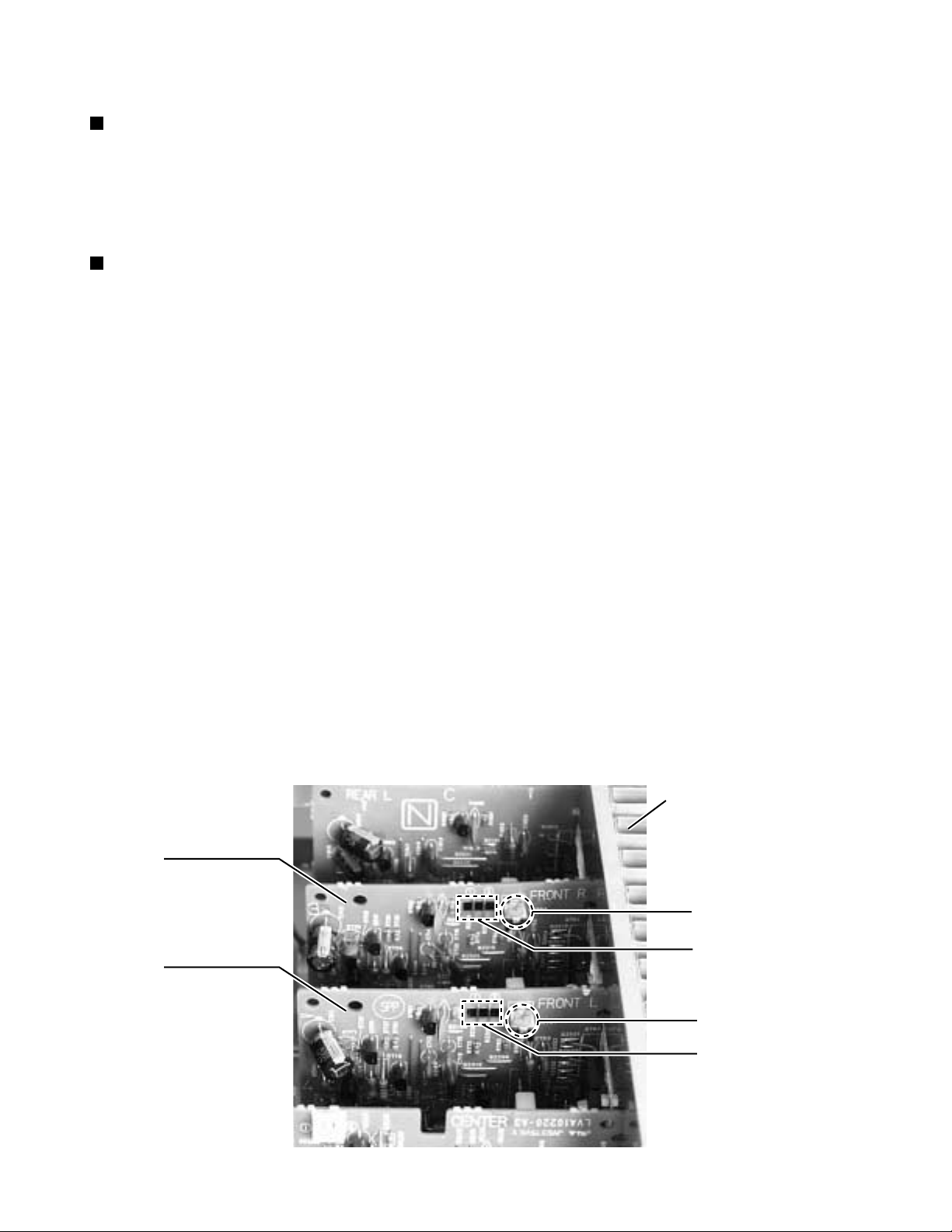
AUDIO/VIDEO CONTROL RECEIVER
RX-8020VBK
Area suffix
RX-8020VBK
A/V CONTROL RECEIVER
CATV/DBS VCR1 TV AUDIO
DVD MULTIDVD
CD
CDR
TV/DBS VIDEO PHONO
TAPE/MD
VCR1 VCR 2
SURR/DSP
ANALOG/DIGITAL
DSP
SURROUND
OFF
ANALOG
BASS
DIRECT
BOOST FRONT•L
231
MENU
SOUND
TEST CENTER SUBWFR
564
ENTER
SURR•L SURR•R
DIMMER
7/P
89
SBACK•L SBACK•R
DIGITAL EQ
MUTING
0
10
RETURN FM MODE 100
CATV/DBS
CONTROL
CH/
LEVEL
TV VOL
TV/VIDEO
TEXT
PLAY
MENU
DISPLAY
REC
/REW
PAUSE
PAUSE
SET
DOWN – TUNING – UP
SLEEP
CONTROL
STOP
RM-SRX8020J
REMOTE CONTROL
FM/AM
USB
INPUT
FRONT•R
+10
+
VOLUME
EXIT
FF/
SPEAKERS ON/OFF
SUBWOOFER OUT ON/OFF
PHONES
STANDBY
STANDBY/ON
1
2
FM/AM TUNING FM/AM PRESET FM MODE
SURROUND
Contents
USB AUDIO
PUSH OPEN
DSP
S-VIDEO VIDEO
MEMORY
SURROUND/DSP
OFF
VIDEO
L—AUDIO—R
INPUT
ANALOG/DIGITAL
INPUT ATT
RX-8020V
AUDIO/VIDEO CONTROL RECEIVER
SOURCE NAME
TV SOUND/DBSVIDEOVCR 2VCR 1DVDDVD MULTI
SOUCE NAME
FM/AMUSB AUDIOTAPE/MDCDRCDPHONO
DIGITAL
EQ
EFFECT SETTING
CONTROL
DOWN UP
UJ ---------- U.S.Military
MASTER VOLUME
LEVEL
ADJUST
ANALOG DIRECT
BASS BOOST
Safety precautions --------------------------------------------------------1-2
Disassembly method -----------------------------------------------------1-3
Adjustment method -------------------------------------------------------1-9
Self-diagnose function-----------------------------------------------------1-10
Description of major ICs -------------------------------------------------1-12~31
COPYRIGHT 2002 VICTOR COMPANY OF JAPAN, LTD.
No.21161
Oct. 2002
Page 2
RX-8020VBK
1. This design of this product contains special hardware and many circuits and components specially for safety
purposes. For continued protection, no changes should be made to the original design unless authorized in
writing by the manufacturer. Replacement parts must be identical to those used in the original circuits. Services
should be performed by qualified personnel only.
2. Alterations of the design or circuitry of the product should not be made. Any design alterations of the product
should not be made. Any design alterations or additions will void the manufacturer`s warranty and will further
relieve the manufacture of responsibility for personal injury or property damage resulting therefrom.
3. Many electrical and mechanical parts in the products have special safety-related characteristics. These
characteristics are often not evident from visual inspection nor can the protection afforded by them necessarily
be obtained by using replacement components rated for higher voltage, wattage, etc. Replacement parts which
have these special safety characteristics are identified in the Parts List of Service Manual. Electrical
components having such features are identified by shading on the schematics and by ( ) on the Parts List in
the Service Manual. The use of a substitute replacement which does not have the same safety characteristics
as the recommended replacement parts shown in the Parts List of Service Manual may create shock, fire, or
other hazards.
4. The leads in the products are routed and dressed with ties, clamps, tubings, barriers and the like to be
separated from live parts, high temperature parts, moving parts and/or sharp edges for the prevention of
electric shock and fire hazard. When service is required, the original lead routing and dress should be
observed, and it should be confirmed that they have been returned to normal, after re-assembling.
5. Leakage currnet check (Electrical shock hazard testing)
After re-assembling the product, always perform an isolation check on the exposed metal parts of the product
(antenna terminals, knobs, metal cabinet, screw heads, headphone jack, control shafts, etc.) to be sure the
product is safe to operate without danger of electrical shock.
Do not use a line isolation transformer during this check.
Plug the AC line cord directly into the AC outlet. Using a "Leakage Current Tester", measure the leakage
current from each exposed metal parts of the cabinet, particularly any exposed metal part having a return
path to the chassis, to a known good earth ground. Any leakage current must not exceed 0.5mA AC (r.m.s.).
Alternate check method
Plug the AC line cord directly into the AC outlet. Use an AC voltmeter having, 1,000 ohms per volt or more
sensitivity in the following manner. Connect a 1,500 10W resistor paralleled by a 0.15 F AC-type capacitor
between an exposed metal part and a known good earth ground.
Measure the AC voltage across the resistor with the AC
voltmeter.
Move the resistor connection to each exposed metal part,
particularly any exposed metal part having a return path to
the chassis, and meausre the AC voltage across the resistor.
Now, reverse the plug in the AC outlet and repeat each
measurement. Voltage measured any must not exceed 0.75 V
AC (r.m.s.). This corresponds to 0.5 mA AC (r.m.s.).
0.15 F AC TYPE
1500 10W
Good earth ground
AC VOLTMETER
(Having 1000
ohms/volts,
or more sensitivity)
Place this
probe on
each exposed
metal part.
!
1. This equipment has been designed and manufactured to meet international safety standards.
2. It is the legal responsibility of the repairer to ensure that these safety standards are maintained.
3. Repairs m ust be made in accordance with the relevant safety standards.
4. It is essential that safety critical components are replaced by approved parts.
5. If mains voltage selector is provided, check setting for local voltage.
Burrs formed during molding may
be left over on some parts of the
chassis. Therefore, pay attention to
such burrs in the case of
preforming repair of this system.
In regard with component parts appearing on the silk-screen pr inted side (parts side) of the PWB diagrams, the
parts that are printed over with black such as the resistor ( ), diode ( ) and ICP ( ) or identified by the " "
mark nearby are critical for safety.
(This regulation does not correspond to J and C version.)
1-2
Page 3
RX-8020VBK
Disassembly method
Removing the top cover (See Fig.1)
1.
Remove the four screws A attaching the top cover
on both sides of the body.
2.
Remove the three screws B on the back of the body.
3.
Remove the top cover from behind in the direction of
the arrow while pulling both sides outward.
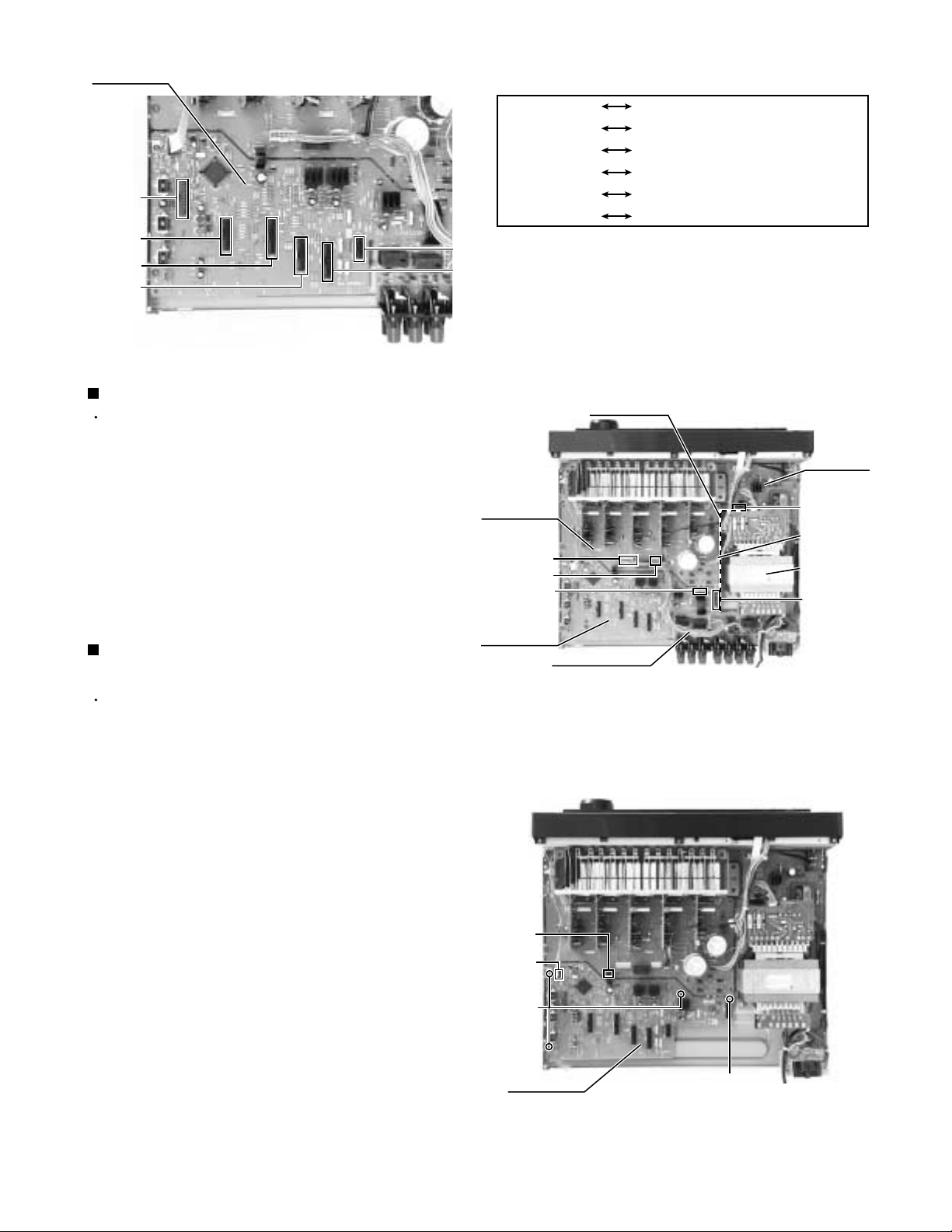
Removing the front panel assembly
(See Fig.2 and 3)
Prior to performing the following procedure, remove
the top cover.
1.
Cut off the tie bands.
2.
Disconnect the harness from the connector CN416
(on the video audio board), CN206 (on the video
board) and CN244 (on the S video board) (see fig.8).
3.
Disconnect the card wire from the connector CN400
on the audio board and CN402 on the power supply
board.
4.
Remove the three screws C fixing the upper surface
of the front panel, and four screws D fixing the
bottom.
Main
board
Audio
board
CN400
Top cover
C
A
(both sides)
B
Fig.1
Front panel assembly
C
Power
supply board
CN402
Tie band
Compu
link board
CN393
Fig.2
5.
Detach the front panel assembly toward the front.
6.
Remove the screw X attaching the earth wire (see fig.
19).
Removing the compulink board
(See Fig.2 and 4)
Prior to performing the following procedure, remove
the top cover.
1.
Disconnect the harness from the connector CN393
on the compu link board.
2.
Remove the three screws E attaching the compu link
board to the rear panel.
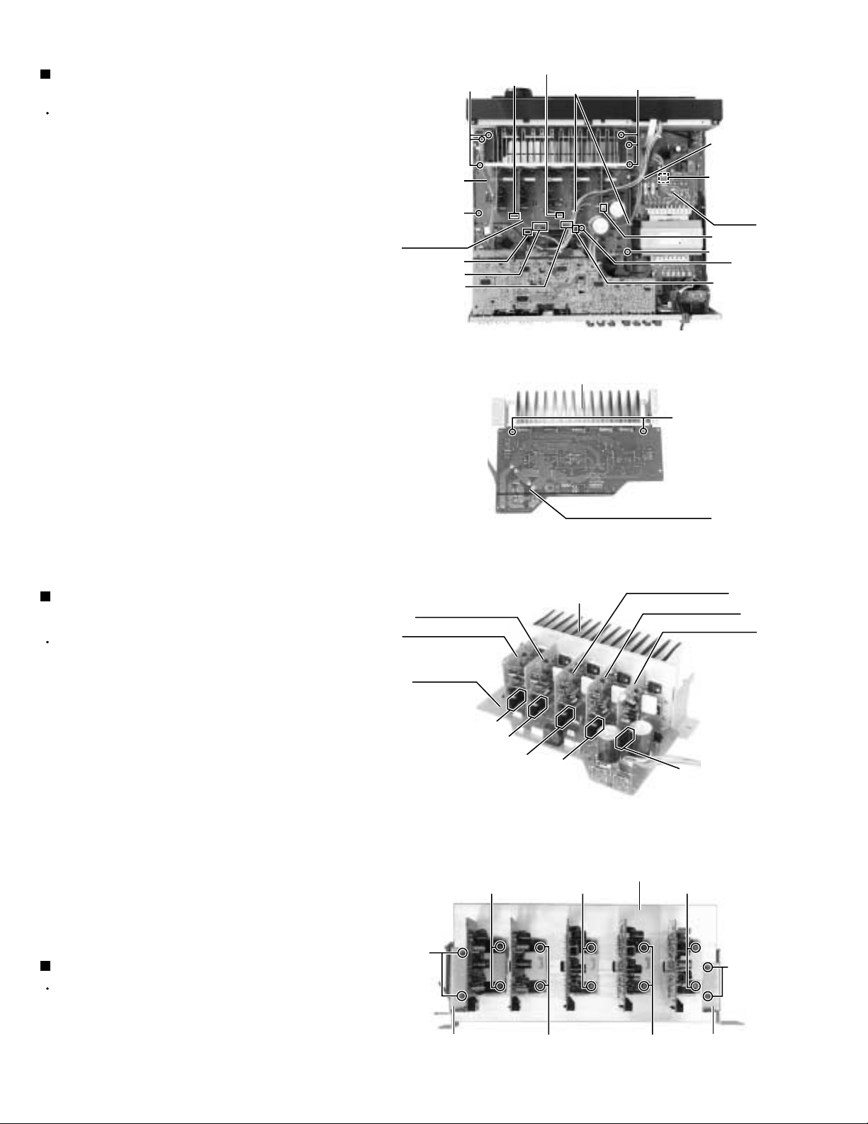
Removing the rear panel (See Fig.4)
Prior to performing the following procedure, remove
the top cover.
1.
Remove the power cord stopper from the rear panel
by moving it in the direction of the arrow.
D
Front panel assembly
Fig.3
Cord stopper
FFF FE G
2.
Remove the thirty seven screws E & F & G & H
attaching the each board to the rear panel.
3.
Remove the three screws I attaching the rear panel
on the back of the body.
Rear panel
FIIHI
Fig.4
1-3
Page 4
RX-8020VBK
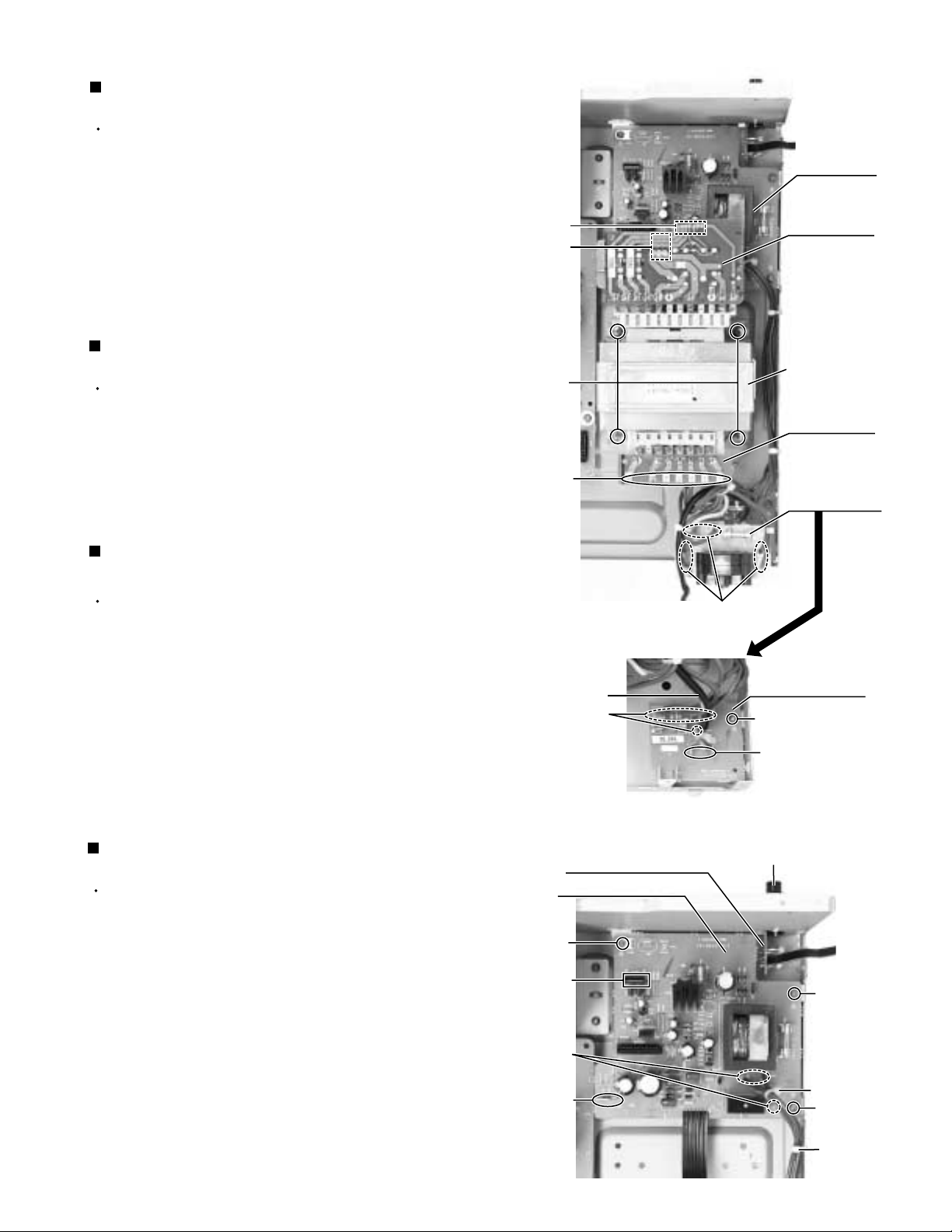
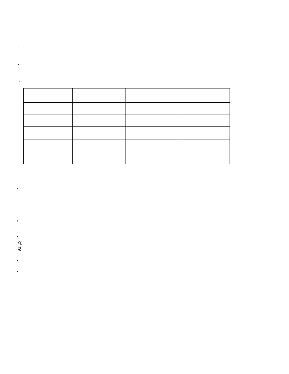
Removing the DVD board (See Fig.5 and 6)
Prior to performing the following procedure, remove
the top cover and rear panel.
1.
Cut off the tie bands.
2.
Disconnect the harness from the connector CN393
on the compu link board (see fig.2).
3.
Disconnect the harness from the connector CN721,
CN723 on the main board and CN722 on the Cch
amp. board.
4.
Remove the two fasteners fixing the small board to
the audio input board and video board.
5.
Draw out the DVD board upwards, disconnecting the
connector CN501, CN243, CN205, CN381 and
CN361 on the DVD board.
Removing the each board of the tuner, the
audio input, the video audio, the video, the
S video and the DSP (See Fig.7 to 10)
Main
board
CN721
CN723
CN361
CN381
CN205
Small board
Fastener
Video audio board
Audio input board
Audio input board
&
Video board
Video board
CN722
(on the Cch
amp. board)
Tie band
DVD board
CN501
CN243
Fig.5
DVD board
Fig.6
S Video board
DSP board
Prior to performing the following procedure, remove
the top cover, rear panel and DVD board.
1.
Remove the tuner board from the connector CN101
on the audio board.
2.
Remove the audio input board from the connector
CN301 on the audio board.
3.
Disconnect the harness from the connector CN416
and remove the video audio board from the
connector CN303 on the audio board.
4.
Disconnect the harness from the connector CN206
and remove the video board from the connector
CN201 on the audio board.
6.
Disconnect the harness from the connector CN244
and remove the S video board from the connector
CN241 on the audio board.
7.
Remove the DSP board from the connector CN601
on the audio board.
Tuner board
Fig.7
CN244
(on the S
video board)
1-4
CN206
(on the
video board)
CN416
(on the video audio board)
Fig.8
Page 5
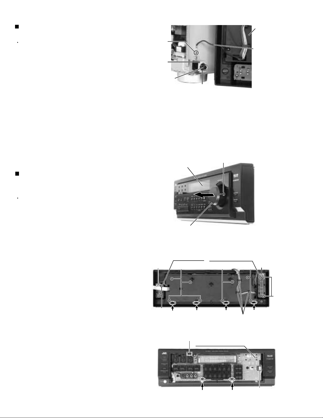
RX-8020VBK
Audio board
CN101
CN301
CN303
CN201
Fig.9
Removing the speaker board (See Fig.11)
Prior to performing the following procedure, remove
the top cover and rear panel.
Disconnect the harness from the connector CN931/
1.
CN932 on the audio board.
Disconnect the harness from the connector CN813
2.
and CN814 on the main board.
CN601
CN241
Main board
Connection between the audio board and each board
CN101
CN301
CN303
CN201
CN241
CN601
Tuner board (CN111)
Audio input board (CN311)
Vidoe audio board (CN313)
Video board (CN200)
S video board (CN240)
DSP board (CN587)
Fig.10
Relay board
Power
supply
board
CN71
Tie band
CN814
CN813
CN931
/CN932
Power
transformer
CN81
Removing the audio board
(See Fig.11 and 12)
Prior to performing the following procedure, remove
the top cover, rear panel, DVD board, tuner board,
audio input board, video audio board, video board, S
video board and DSP board.
Disconnect the harness and card wire from the
1.
connector CN931 /CN932 and CN400 on the audio
board.
Cut off the tie band, if needed.
2.
Disconnect the connector CN71(on the power supply
3.
board) and CN81(on the audio board) and remove the
relay board.
Disconnect the harness from the connector CN831 on
4.
the main board.
Remove the three screws J and screw K attaching the
5.
audio board.
Audio board
CN831
CN400
J
Audio board
Speaker board
Fig.11
K
Fig.12
1-5
Page 6
RX-8020VBK
Removing the main board
(See Fig.13 to 15)
Prior to performing the following procedure, remove
the top cover.
1.
Remove the card wire and cut off the tie bands.
2.
Disconnect the harness from the connector CN721,
CN723, CN813, CN814, CN831 and CN881 on the
main board.
3.
Disconnect the harness from the connector CN722
on the Cch amp. board (see fig.5).
4.
Disconnect the harness from the connector CN811
on the power trans1 board.
6.
Remove the screw K, after removing the relay board
if needed (see fig.11).
7.
Remove the two screws L and the six screws M
attaching the main board.
8.
Remove the two screws N attaching the heat sink to
the main board.
9.
Disconnect the connector of each amp. board.
Card wire
L
Main board
CN831
CN814
CN813
M
CN723
CN721
Tie band
Fig.13
Heat sink
Main board (reverse side)
Fig.14
M
N
Tie band
CN811
Power
trans1
board
CN722
K
L
CN881
Removing the each amp. board of Cch,
Lch, Rch, RLch and RRch (See Fig.16)
Prior to performing the following procedure, remove
the top cover and main board.
1.
Remove the two screws O attaching the Cch amp.
board and remove the Cch amp. board.
2.
Remove the two screws P attaching the Lch amp.
board and remove the Lch amp. board.
3.
Remove the two screws Q attaching the Rch amp.
board and remove the Rch amp. board.
4.
Remove the two screws R attaching the RLch amp.
board and remove the SLch amp. board.
5.
Remove the two screws S attaching the RRch amp.
board and remove the SRch amp. board.
Removing the Heat sink (See Fig.16)
Prior to performing the following procedure, remove
the top cover, main board and each amp. board.
RLch amp. board
RRch amp. board
Main board
CN706
CN705
CN702
S
T
(RRch)
Heat sink
CN701
Fig.15
Q
(Rch)
Rch amp. board
Lch amp. board
Cch amp. board
Heat sink
CN703
O
(Cch)
T
Remove the four screws T attaching the two
1.
brackets to the heat sink and remove the two
brackets.
1-6
Bracket
R
(RLch)
Fig.16
P
(Lch)
Bracket
Page 7
Removing the power transformer
(See Fig.17)
Prior to performing the following procedures, remove
the top cover.
1.
Disconnect the harness from the connector CN55
/CN56 and CN811 on the power trans1 board.
2.
Unsolder the seven solder parts on the power trans2
board.
3.
Remove the four screws U attaching the power
transformer.
Removing the voltage selector board
(See Fig.17)
Prior to performing the following procedure, remove
the top cover.
1.
Removed the two screws G attaching the voltage
selector board to the rear panel (see fig.4).
2.
Unsolder the six solder parts on the voltage selector
board.
CN55/CN56
CN811
U
Solder part
RX-8020VBK
Power
supply board
Power
trans1 board
Power
transformer
Power
trans2 board
Voltage
selector board
Removing the power/fuse board
(See Fig.17)
Prior to performing the following procedure, remove
the top cover.
1.
Removed the two screws G attaching the voltage
selector board to the rear panel (see fig.4).
2.
Remove the screw H attaching the power/fuse board
to the rear panel (see fig.4).
3.
Remove the screw V attaching the power/fuse board.
4.
Unsolder the eight solder parts on the power/fuse
board.
Removing the power supply board
(See Fig.18)
Prior to performing the following procedure, remove
the top cover and relay board.
1.
Cut off the tie band if needed.
2.
Disconnect the card wire from the connector CN402
on the power supply board.
Power cord
Solder part
(on the reverse side)
Headphone jack board
Power supply board
W
CN402
Solder part
(on the reverse side)
Fig.17
Under this board
Power/fuse board
V
Solder part
Headphone jack
W
3.
Disconnect the harness from the connector
CN55/CN56 on the power trans1 board (see fig.17).
4.
Remove the three screws W attaching the power
supply board and pull out the power supply board
removing the hook.
5.
Unsolder the three solder parts on the power supply
board.
Solder part
(on the
reverse side)
Hook
Fig.18
Tie band
W
Tie band
1-7
Page 8
RX-8020VBK
g
)
Removing the headphone jack board
(See Fig.18 and 19)
Prior to performing the following procedure, remove
the top cover, front panel assembly and power supply
board.
1.
Disconnect the harness form the connector CN881
on the main board (see fig.13).
2.
Remove the nut fixing the headphone jack.
3.
Drawn out the headphone jack board in the direction
of an inner side.
<Front panel assembly>
Removing the system control board,
power switch board and switch board
(See Fig.1 to 3)
Prior to performing the following procedure, remove
the top cover and front panel assembly.
X
Bracket
Headphone
jack
Operation switch panel
Front panel
assembly
(inner side)
Earth wire
Nut
Fig.19
Nut
1.
Pull out the volume knob on the front side of the front
panel assembly and remove the nut attaching the
system control board.
2.
Remove the two screws A attaching the power
switch board on the front panel assembly(inner side).
And disconnect the harness from the connector
CN430 on the power switch board.
3.
Remove the two screws B attaching the switch board
on the front panel assembly(inner side). And
disconnect the harness form the connector CN432
on the switch board.
4.
Remove the harness from the three hooks a.
5.
Remove the eight screws C attaching the operation
switch panel from the inner side of the front panel
assembly.
6.
Release the four joints on the front panel assembly
(inner side) by pushing the joint tabs inward.
Remove the operation switch panel toward the front.
7.
Release the two hooks b attaching the system
control board.
CN432
B
Volume knob
Switch board
C
Joint
CN412
Fig.1
Front panel assembly (inner side
Power switch board
C
Joint
System control board
Joint
Fig.2
Hook a
C
Joint
CN430
A
8.
Disconnect the card wire from the connector CN410
and CN412 on the system control board.
1-8
Hook b
Fi
.3
Hook b
CN410
Page 9
Adjustment method
Tuner section
1.Tuner range
FM 87.5MHz~108.0MHz
AM(MW) 531 kHz to 1 602 kHz (at 9 kHz intervals)
530 kHz to 1 600 kHz (at 10 kHz intervals)
Power amplifier section
Adjustment of idling current
Measurement location B2204-B2205(Lch) , B2213-2214(Rch)
Adjustment part VR787(Lch) , VR788(Rch)
Attention
This adjustment does not obtain a correct adjustment value immediately after the amplifier is
used (state that an internal temperature has risen).
Please adjust, after you turn off amplifier and internal temperature falls.
RX-8020VBK
<Adjustment method>
1.Set the volume control to minimum during this adjustment.(No signal & No load)
2.Set the surround mode OFF.
2.Turn VR787 and VR788 fully counterclockwise to warm up before adjustment.
If the heat sink is already warm from previous use the correct adjustment can not be made.
3.For L-ch,connect a DC voltmeter between B2204 and B2205 (Lch)
And,connect it between B2213 and B2214(Rch).
4.30 minutes later after power on, adjust VR787 for L-ch, or VR788 for R-ch so that the DC voltmeter
value has 1mV~10mV.
* It is not abnormal though the idling current might not become 0mA even if it is finished to turn variable
resistance (VR787,VR788) in the direction of counterclockwise.
Heat sink
Rch amp. board
VR788 (Rch)
Lch amp. board
B2213, B2214
VR787 (Lch)
B2204, B2205
1-9
Page 10
RX-8020VBK
Self-diagnose function
1. Detection of abnormal power supply and voltage
When the power is turned ON, if an abnormality is detected during the signal input at the A/D port (IC901,
pin 2-5, 7) for one second continuously, the status will become STANDBY mode immediately.
When the power is turned ON again, detection of abnormal power supply and voltage will not be carried out
during the first 4 seconds.
Given below is a list of threshold values at the detection of abnormalities.
Pin 2
Micro-computer+5V
Pin 3
Digital+5V
Pin 4
Analog+5V
Pin 5
+12V
Pin 7
Tuner+9V
At abnormal state
(Low voltage)
Analog value
0 - 2.2V
Analog value
0 - 2.2V
Analog value
0 - 2.2V
Analog value
0 - 2.2V
Analog value
0 - 2.2V
At normal state
Analog value
2.2 - 2.8V
Analog value
2.2 - 2.8V
Analog value
2.2 - 2.8V
Analog value
2.2 - 2.8V
Analog value
2.2 - 2.8V
At abnormal state
(High voltage)
Analog value
2.8 - 5.0V
Analog value
2.8 - 5.0V
Analog value
2.8 - 5.0V
Analog value
2.8 - 5.0V
Analog value
2.8 - 5.0V
2. Initial setting on ship
To gain the initial setting on ship, put the power plug in the socket while pressing "DOWN" key and "UP" key
together simultaneously, then turn the power ON.
3. Test mode
To enter the test mode, put the power plug in the socket while pressing "EFFECT" key and "UP" key together
simultaneously, then turn the power ON.
Workings of test mode:
All FLs are turned ON for 3 seconds. (the FLs, which are divided in two groups, are turned ON alternatively)
A Faster volume UP/DOWN operation can be achieved with the remote controller.
When the power is turned OFF, the test mode will be released.
The FL display returns to normal after the three seconds. Then the STANDBY LED is turned ON (flashing
ON and OFF for each one second) to show the present status being a test mode.
1-10
Page 11

RX-8020VBK
4. Self-diagnose
To enter the self-diagnose mode, put the power plug in the socket while pressing "SETTING" key and "UP" key
together simultaneously, then turn the power ON.
While the working status is being displayed, the each item can be switched with the UP/DOWN key
operation.
When the power is turned OFF, the self-diagnose mode will be released.
During the self-diagnose mode, the STANDBY LED is turned ON (flashing ON for one second then OFF for
three seconds).
FL transient display will be carried out as follows. When the transient display is not carried out,
normal display/workings are carried out.
S0001
200202209
V
D1
D2
D3
D4
D5
D6
D7
e
r
0
2
/
0
D
S
P
R
A
N
A
D
D
D
D
D
D
U
F
F
F
F
N
G
U
N
P
C
A
C
A
C
D
D
D
A
A
M
P
N
G
U
N
1
2
2
2
3
2
3
2
3
N
G
L
I
G
I
I
G
I
I
G
I
I
G
I
I
G
I
I
G
I
N
L
O
s
3
s
4
s
4
s
9
D
L
O
M
3
3
T
T
T
S
S
S
-
C
E
G
D
L
O
/
0
.
/
0
.
/
0
.
/
0
.
/
0
.
/
1
.
/
1
.
/
2
.
/
2
.
D
Information on VERSION of system microcomputer (IC901)
Example : 2002/2/20 9th ROM
1
.
0
Display the local version (IC581)
0
Example : Ver_1.00
2
/
1
Display the local creation date
0
Example : 2002/2/10
e
v
4
Display the DSP version (IC511)
1
Example : DSP Rev41
O
G
x
T
A
L
T
A
L
T
A
L
T
A
L
T
A
L
T
A
L
C
2
4
8
6
A
C
E
E
E
A
C
0
0
0
0
0
0
0
0
0
A
K
H
k
H
k
H
k
H
k
T
A
K
X
S
S
A
T
K
L
D
T
A
Display the input sources
x
1
However, since it is the source of DIR processing, actual source may be
2
3
contradicted.
4
Example : ANALOG08
5
Display the input Fs
z
Example : Fs48kHz
z
z
z
Display the input format
Example : PCM
M
D
Display the input channel
Example : 2/0.0
t
M
1-11
Page 12

RX-8020VBK
Description of major ICs
XCC56367PV150 (IC501) : DSP
1. Pin layout
MISO/SDA
144
HREQ#
VCCS
GNDS
FST
FSR
SCKT
SCKR
HCKT
HCKR
VCCQL
GNDQ
VCCQH
VCCS
GNDS
ADO
ACI
TIO0
HAD7
HAD6
HAD5
1
2
3
4
5
6
7
8
9
10
11
12
13
14
15
16
17
18
19
20
21
22
23
24
25
26
27
28
29
30
31
32
33
34
35
36
37
HAD4
2. Block diagram
SCK/SCL
SS#/HA2
SDO0/SDO0_1
SDO2/SDI3/SDO2_1/SDI3_1
SDO3/SDI2/SDO3_1/SDI2_1
SDO1/SDO1_1
SDO4/SDI1
SDO5/SDI0
HDS/HWR
HRW/HRD
HACK/HRRQ
HOREQ/HTRQ
HCS/HA10
HA9/HA2
HA8/HA1
HAS/HA0
MOSI/HA0
TMS
TCK
143
142
141
38
39
40
HAD3
VCCH
GNDH
TDI
TDO
SDO4_1/SDI1_1
MODA/IRQA#
140
139
138
137
41
42
43
44
HAD2
HAD1
HAD0
RESET#
MODB/IRQB#
MODCIRQC#
MODD/IRQD#
D23
D22
136
135
134
133
132
45
46
47
48
49
PCAP
VCCP
GNDP
VCCQH
SDO5_1/SDI0_1
D21
GNDD
131
130
50
51
AA2
FST_1
VCCD
D20
129
128
52
53
CAS#
SCKT_1
GNDQ
VCCQL
127
126
54
55
GNDQ
EXTAL
D19
D18
125
124
56
57
VCCC
VCCQL
D17
D16
123
122
58
59
GNDC
FSR_1
D15
GNDD
121
120
60
61
SCKR_1
PINT/NMI#
VCCD
D14
119
118
62
63
TA#
BR#
D13
117
64
BB#
D12
D11
116
115
65
66
VCCC
GNDC
D10D9GNDD
VCCDD8D7
114
113
112
111
67
68
69
70
AA1
AA0
RD#
WR#
110
71
BG#
109
108
107
106
105
104
103
102
101
100
99
98
97
96
95
94
93
92
91
90
89
88
87
86
85
84
83
82
81
80
79
78
77
76
75
74
73
72
A0
D6
D5
D4
D3
GNDD
VCCD
D2
D1
D0
A17
A16
A15
GNDA
VCCQH
A14
A13
A12
VCCQL
GNDQ
A11
A10
GNDA
VCCA
A9
A8
A7
A6
GNDA
VCCA
A5
A4
A3
A2
GNDA
VCCA
A1
1-12
1 2 16 8 4 6
TRIPLE
TIMER
DAX
(SPDIF Tx.)
INTERFACE
HOST
INTERFACE
ESAI
INTERFACE
ESAI_1
ADDRESS
PIO_EB
GENERATION
UNIT
SIX CHANNELS
DMA UNIT
24-BIT
DSP56300
Core
INTERNAL
DATA
BUS
PLL
CLOCK
GENARAT
EXTAL
RESET
PINIT/NMI
PROGRAM
INTERRUPT
CONTROLLER
PROGRAM
DECODE
CONTROLLE
MODA/IRQA
MODB/IRQB
MODC/IRQC
MODD/IRQD
5
SHI
INTERFACE
PERIPHERAL
EXPANSION AREA
PROGRAM
ADDRESS
GENERATOR
MENORY EXPANTION AREA
PROGRAM
RAM
/INSTR.
CACHE
3Kx24
PROGRAM
ROM
40K x 24
Bootstrap
PM_EB
X MEMORY
RAM
13K x 24
ROM
32K x 24
XM_EB YM_EB
YAB
XAB
PAB
DAB
DDB
YDB
XDB
PDB
GDB
DATA ALU
24 x 24 + 56->56-BIT MAC
TWO 56-BIT ACCUMULATORS
BARREL SHIFTER
24BITS BUS
Y MEMORY
RAM
7K x 24
ROM
8K x 24
EXTERNAL
ADDRESS
SRAM BUS
INTERFACE
EXTERNAL
DATA BUS
BUS
SWITCH
DRAM &
&
I-CACHE
SWITCH
POWER
MNGMNT
JTAG
OnCE
18
ADDRESS
10
CONTROL
24
DATA
4
Page 13

3. Signal groupings
RX-8020VBK
PORT A ADDRESS BUS
A0-A17
VCCA(3)
GNDA(4)
PORT A DATA BUS
D0-D23
VCCD(4)
GNDD(4)
PORT A BUS CONTROL
AA0-AA2/RAS0-RAS2
CAS
RD
WR
TA
BR
BG
BB
VCCC(2)
GNDC(2)
INTERRUPT AND
MODEL CONTROL
MODA/IRQA
MODB/IRQB
MODC/IRQC
MODD/IRQD
RESET
PLL AND CLOCK
EXTAL
PINIT/NMI
PCAP
VCCP
GNDP
QUIET POWER
VCCQH(3)
VCCQL(4)
GNDQ(4)
SPDIF TRANSMITTER(DAX)
ADO[PD1]
ACI[PD0]
TIMER 0
TIO0[TIO0]
Port D
Port B
Port C
Port E
OnCE ON-CHIP EMULATION/JTAG PORT
TDI
TCK
TDO
TMS
PARALLEL HOST PORT(HD108)
HAD(7:0)[PB0-PB7]
HAS/HA0[PB8]
HA8/HA1[PB9]
HA9/HA2[PB10]
HRW/HRD[PB11]
HDS/HWR[PB12]
HCS/HA10[PB13]
HOREQ/HTRQ[PB14]
HACK/HRRQ[PB15]
VCGH
GNDH
SERIAL AUDIO INTERFACE (ESAI)
SCKT[PC3]
FST[PC4]
HCKT[PC5]
SCKR[PC0]
FSR[PC1]
HCKR[PC2]
SDO0[PC11]/SDO0_1[PE11]
SDO1[PC10]/SDO1_1[PE10]
SDO2/SDI3]PC9]/SDO2_1/SDI3_1[PE9]
SDO3/SDI2[PC8]/SDO3_1/SDI2_1[PE8]
SDO4/SDI1[PC7]
SDO5/SDI0[PC6]
SERIAL AUDIO INTERFACE (ESAI_1)
SCKT_1[PE3]
FST_1[PE4]
SCKR_1[PE0]
FSR_1[PE1]
SDO4_1/SDI1_1[PE7]
SDO5_1/SDI0_1[PE6]
VCCS(2)
GNDS(2)
SERIAL HOST INTERFACE (SHI)
MOSI/HA0
SS/HA2
MISO/SDA
SCK/SCL
HREQ
1-13
Page 14

RX-8020VBK
AK4586VQ (IC571) : DIR & CODEC
1. Pin layout
44 - 34
2. Pin function
Pin No.
1
2
3
4
5
6
7
8
9
10
11
12
13
14
15
16
17
18
19
20
21
22
23
24
25
26
27
28
29
30
31
32
33
34
35
36
37
38
39
40
41
42
43
44
1-14
11 - 1
12 - 22
Symbol
XTO
XTI
EXTCLK
TVDD
VDSS
DVDD
TX
MCKO
LRCK
BICK
SDTO
SDTI1
SDTI2
SDTI3
INT0
INT2
CDTO
CAD1
CDTI
SDA
CCLK
SCL
CSN
CAD0
DZF2
OVF
AVSS
AVDD
VREFH
VCOM
DZF1
LOUT3
ROUT3
LOUT2
ROUT2
LOUT1
ROUT1
LIN
RIN
PCDD
R
PVSS
RX4
SLAVE
RX3
TST
RX2
I2C
RX1
PDN
23 - 33
I/O
O
I
I
-
-
O
O
I/O
I/O
O
I
I
I
O
O
O
I
I
I/O
I
I
I
I
O
O
-
-
I
O
O
O
O
O
O
O
O
I
I
-
-
-
I
I
I
I
I
I
I
I
Function
X'tal output pin
X'tal input pin
External master clock input pin
Output buffer power supply pin, 2.7V~5.5V
Digital Ground pin, 0V
Digital power supply pin, 4.5V~5.5V
Transmit channel (through data) output pin
Master clock output pin
Input/Output channel clock pin
Audio serial data clock pin
Audio serial data output pin
DAC1 audio serial data input pin
DAC2 audio serial data input pin
DAC3 audio serial data input pin
Interrupt 0 pin
Interrupt 1 pin
Control data output pin in 4-wire serial control mode
Chip address 1 pin in I2C bus control mode
Control data input pin in 4-wire serial control mode
Control data input/output pin in I2C bus control mode
Control data clock pin in 4-wire serial control mode
Control data clock pin in I2C bus control mode
Chip select pin in 4-wire serial control mode
Chip address 0 pin in I2C bus control mode
Zero input detect 2 pin
Analog input overflow detect pin
Analog ground pin, 0V
Analog power supply pin, 4.5V~5.5V
Positive voltage reference input pin, AVDD
Common voltage output pin, AVDD/2
Zero input detect 1 pin
DAC3 Lch analog output pin
DAC3 Rch analog output pin
DAC2 Lch analog output
DAC2 Rch analog output pin
DAC1 Lch analog output pin
DAC1 Rch analog output pin
Lch analog input pin
Rch analog input pin
PLL power supply pin, 4.5V~5.5V
External resistor pin
Pll ground pin, 0V
Receiver channel 4 pin (internal biased pin)
Slave mode pin
Receiver channel 3 pin (internal biased pin)
Test pin
Receiver channel 2 pin (internal biased pin)
Control mode select pin
Receiver channel 1 pin internal biased pin)
Power-Down & Reset pin
Page 15

3. Block diagram
CSN
CCLK
CDTI
RX-8020VBK
CDTO
LIN
RIN
LOUT1
ROUT1
LOUT2
ROUT2
LOUT3
ROUT3
ADC HPF
ADC HPF
DAC DA TTLPF
DAC DA TTLPF
DAC DA TTLPF
DAC DA TTLPF
DAC DA TTLPF
DAC DA TTLPF
Audio
I/F
MCLK
SDOUT
BICK
LRCK
SDIN1
SDIN2
SDIN3
uP I/F
Clock
Recovery
DAIF
Decoder
DEM
X'tal
Oscillator
Clock
Generator
Input
Selector
XTI
XTO
MCKO
TX
RX1
RX2
RX3
RX4
SDOUT
BICK
LRCK
SDIN1
SDIN2
SDIN3
IS63LV102410K-X (IC512, IC513, IC514) : CMOS SRAM
1. Pin layout 2. Pin function
1
A0
A1
A2
A3
CE
I/O0
I/O1
Vcc
GND
I/O2
I/O3
WE
A4
A5
A6
A7
2
3
4
5
6
7
8
9
10
11
12
13
14
15
16
32
31
30
29
28
27
26
25
24
23
22
21
20
19
18
17
A16
A15
A14
A13
OE
I/O7
I/O6
GND
Vcc
I/O5
I/O4
A12
A11
A10
A9
A8
Symbol
A0-A16
CE
OE
WE
I/O1-I/O7
Vcc
GND
Function
Address Input
Chip Enacble Input
Output Enable Input
Write Enable Input
Bidirectional Ports
Power
Ground
3. Block diagram
A0-A16
VCC
GND
I/O0-I/O7
CE
OE
WE
DECODER
I/O
DATA
CIRCUIT
CONTROL
CIRCUIT
128K X 8
MEMORY ARRAY
COLUMN I/O
1-15
Page 16

RX-8020VBK
MB90088 (IC203) : Display controller
1.Pin layout
YIN
VIN
CIN
AVcc
IOUT
VOC
Vcc
EXS
XS
HSYNC
VSYNC
EXHSYN
EXVSYN
Vss
2.Block diagram
SIN
SCLK
CS
EXHSYN
EXVSYN
1
2
3
4
5
6
7
8
9
10
11
12
13
14
28
AVss
27
YOUT
26
VOUT
25
COUT
24
CS
23
SIN
22
SCLK
21
TEST
20
BOUT
19
ROUT
18
GOUT
17
VOB
16
XD
15
EXD
Serial Input
Control
H/V Separate
Each Control, Data
VIN
YIN
CIN
HSYNC
VSYNC
XS
EXS
XD
EXD
NTSC/PAL
Signal OSC
Display Memory
Control
VRAM
4FSC CLK
OSC
Dot CLK
OSC
Each Block
Each Block
Analog SW
Video Signal
OSC
Output
Control
CGROM
VOUT
YOUT
COUT
BOUT
ROUT
GOUT
IOUT
VOC
VOB
1-16
Page 17

3.Functions
RX-8020VBK
pin
Symbol I/O
no
YIN
1
VIN
2
CIN
3
4
AVcc
5
IOUT
6
VOC
7
Vcc
8
EXS
9
XS
10
HSYNC
11
VSYNC
12
EXHSYN
13
EXVSYN
14
Vss
EXD
15
16
XD
17
VOB
18
GOUT
19
ROUT
20
BOUT
21
TEST
22
SCLK
23
SIN
24
CS
25
COUT
26
VOUT
27
YOUT
28
AVss
Function
I
Lux signal Input terminal for Superinpause indication
I
Composite video signal input terminal for Superinpause indication
Contrast signal input terminal for Superinpause indication
I
-
Analog power supply terminal
O
Color (Lux) signal output terminal
Character output terminal
O
Power supply terminal
Clock generator outside circuit terminal for color burst
I
O
O
Horizontal signal output terminal
O
Vertical signal output terminal
EXT horizontal signal input terminal
I
EXT vertical signal input terminal
I
GND
Dot clock generator outside circuit signal terminal for indication
I
O
Character & background signal output terminal
O
Color signal (Green, Red, Blue)
O
I
Test signal input terminal
Shift clock input terminal for serial transmission
I
Serial data input terminal
I
Chip select terminal
I
Contrast signal output terminal
O
Composite video signal output terminal
O
O
Lux signal output terminal
Analog GND terminal
-
NJM2285V-W (IC202) : 2-input 3-channel video switch
IN1A GND1 IN2B V CTL2 IN2A GND3 IN3B
16 15 14 13 12 11 10 9
BIAS TYPE
L
H
1 2 3 4 5 6 7 8
IN1B CTL1 OUT1 GND2 OUT2 OUT3 CTL3 IN3A
+
CLAMP TYPE
H
L
CLAMP TYPE
H
L
1-17
Page 18

RX-8020VBK
LA1838(IC102) : FM AM IF AMP&detector, FM MPX decoder
1. Block Diagram
30
ALC
BUFF
FM
S-METER
FM IF
1
2. Pin Function
Pin
Symbol
No.
FM IN
1
AM MIX
2
3
FM IF
AM IF
4
GND
5
6
TUNED
STEREO
7
8
VCC
9
FM DET
10
AM SD
FM VSM
11
AM VSM
12
13
MUTE
14
FM/AM
MONO/ST O
15
29
28
AM
OSC
SD
COMP
S-CLRVE
PM
DET
2
I/O
I
This is an input terminal of FM IF
REG
AM
MIX
AM/FM
IF-BUFF
3
27
FM
RF.AMP
AM IF
4
26
AGC
AM
S-METER
GND
Function
DET
5
signal.
This is an out put terminal for AM
O
mixer.
I
Bypass of FM IF
Input of AM IF Signal.
I
I
This is the device ground terminal.
When the set is tuning, this terminal
O
becomes "L".
O
Stereo indicator output. Stereo "L",
Mono: "H"
III
This is the power supply terminal.
I
FM detect transformer.
I
This is a terminal of AM ceramic filter.
O
Adjust FM SD sensitivity.
O
Adjust AM SD sensitivity.
I/O
When the signal of IF REQ of IC121(
LC72131) appear, the signal of FM/AM
IF output. //Muting control input.
Change over the FM/AM input.
I
"H" :FM, "L" : AM
Stereo : "H", Mono: "L"
25
TUNING
DRIVE
6
24
STEREO
DRIVE
7
22
23
P-DET
VCC
89
Pin
Symbol
No.
16
L OUT
17
R OUT
18
19
20
21
22
23
24
25
26
27
28
29
30
L IN
R IN
RO
LO
IF IN
FM OUT
AM DET
AM AGC
AFC
AM RF
REG
AM OSC
OSC BUFFER
21
DECODER
ANIT-BIRDIE
VCO
384KHz
10
20
STEREO
5N
SW
FF
38k
11
I/O
O
Left channel signal output.
O
Right channel signal output.
Input terminal of the left channel post
I
18
19
MUTE
FF
/
19k
2
12 13
FF
19k
/
LS
Function
17 16
PILOT
DET
14
AMP.
Input terminal of the right channel
I
post AMP.
Mpx Right channel signal output.
O
O
Mpx Left channel signal output.
I
Mpx input terminal
FM detection output.
O
AM detection output.
O
This is an AGC voltage input terminal
I
for AM
I
This is an output terminal of voltage
for FM-AFC.
AM RF signal input.
I
Register value between pin 26 and pin28
O
desides the frequency width of the
input signal.
I
This is a terminal of AM Local
oscillation circuit.
AM Local oscillation Signal output.
O
15
1-18
Page 19

LC72136N (IC121) : PLL frequency synthesizer
1. Pin layout
FM/ST/VCO
2. Block diagram
XT
FM/AM
CE
CLOCK
DO
AM/FM
SDIN
DI
1
2
3
4
5
6
7
8
9
10
11
22
21
20
19
18
17
16
15
14
13
12
XT
GND
LPFOUT
LPFIN
PD
VCC
FMIN
AMIN
IFCONT
IFIN
RX-8020VBK
1
22
16
15
3
4
5
6
17
21
3. Pin function
Pin
Symbol
No.
1
2
3
4
5
6
7
8
9
10
11
XT
FM/AM
CE
DI
CLOCK
DO
FM/ST/VCO
AM/FM
LW
MW
SDIN
Reference
Driver
Swallow Counter
1/2
2B
C
I/F
Power
on
Reset
Function
I/O
X'tal oscillator connect (75kHz)
I
LOW:FM mode
O
When data output/input for 4pin(input) and
I
Swallow Counter
1/16,1/17 4bit
1/16,1/17 4bit
12bit
Programmable
DriverS
Data Shift Register & Latch
7821113
6pin(output): H
Input for receive the serial data from
I
controller
Sync signal input use
I
Data output for Controller
O
Output port
"Low": MW mode
O
Open state after the power on reset
O
Input/output port
I/O
Input/output port
I/O
Data input/output
I/O
Phase
Detector
Charge Pump
Unlock
Detector
Universal
Counter
Pin
No.
12
IFCONT
13
14
15
16
17
18
19
LPFOUT
20
21
22
Symbol
IFIN
AMIN
FMIN
VCC
PD
LPFIN
GND
XT
18
19
20
12
I/O
Function
IF counter signal input
I
IF signal output
O
Not use
-
AM Local OSC signal output
I
FM Local OSC signal input
I
Power suplly(VDD=4.5-5.5V)
When power ON:Reset circuit move
PLL charge pump output(H: Local OSC
O
frequency Height than Reference frequency.
L: Low Agreement: Height impedance)
Input for active lowpassfilter of PLL
I
Output for active lowpassfilter of PLL
O
Connected to GND
X'tal oscillator(75KHz)
I
1-19
Page 20

RX-8020VBK
PCM2702ED-X (IC410) : USB D/A converter
1.Pin layout
XTI
1
V
DD
C
2
DGNDC
3
DD
V
4
DGND
5
D+
6
D-
7
V
BUS
8
DGND
9
PLYBCK
10
SSPND
11
ZERO
12
TEST3
13
TEST2
14
3.Pin function
XTO
VccP
AGNDP
VccL
AGNDL
OUT
V
Vcc
COM
V
AGND
V
OUT
AGNDR
VccR
TEST0
TEST1
2. Block diagram
PLYBCK
28
27
26
25
24
23
L
22
21
20
19
R
18
17
16
15
D+
D-
VBUS
DGNDU
VDDC
DGNDC
SSPDN
USB I/F
MCLK
USB clock
generator
Crystal OSC
XTI
XTO
USB packet
data
WRCLK
FIFO
SPACT
audio
data
RDCLK
ZERO
8x
Oversampling
Digital Filter
System Clock
Audio clock
generator
DGNDP
VDDP
Multi-level
Delta-Sigma
Modulator
VccL
AGNDL
VccR
AGNDR
DAC
DAC
Power supply
VCC AGND VDD DGND
Low-pass
Filter
Low-pass
Filter
VOUTL
VCOM
VOUTR
Pin No.
1
2
3
4
5
6
7
8
9
10
11
12
13
14
15
16
17
18
19
20
21
22
23
24
25
26
27
28
Symbol
XTI
DD
C
V
DGNDC
DD
V
DGND
D+
D-
BUS
V
DGNDU
PLYBCK
SSPND
ZERO
TEST3
TEST2
TEST1
TEST0
VccR
AGNDR
OUT
R
V
AGND
COM
V
Vcc
V
OUT
L
AGNDL
VccL
AGNDP
VccP
XTO
I/O
IN
-
-
-
I/O
I/O
IN
-
OUT
OUT
OUT
IN
IN
IN
IN
-
-
OUT
-
-
-
OUT
-
-
-
-
OUT
Function
Crystal Oscillator Input.
Digital Power Supply for Clock Generator, +3.3V.
Digital Ground for Clock Generator.
Digital Power Supply, +3.3V.
Digital Ground.
USB Differential Input/Output Plus.
USB Differential Input/Output Minus.
USB Bus Power (This pin NEVER consumes the USB bus power).
Digital Ground for USB Transceiver.
Playback flag, active LOW. (LOW: playback, HIGH: idle).
Suspend flag, active LOW. (LOW: suspend, HIGH: operational).
Zero flag, (LOW: Normal, HIGH: ZERO).
Test pin 3. Connect to digital ground.
Test pin 2. Connect to digital ground.
Test pin 1. Connect to digital ground.
Test pin 0. Connect to digital ground.
Analog Supply for R-channel, +5V.
Analog Ground for R-channel.
Analog Output for R-channel.
Analog Ground.
Common for DAC.
Analog Supply, +5V.
Analog output for L-channel.
Analog Ground for L-channel.
Analog Supply for L-channel, +5V.
Analog Ground for PLL.
Analog Supply for PLL, +5V.
Crystal Oscillator Output.
(1)
(2)
(2)
(2)
(2)
(2)
1-20
Note:
(1) 3.3V tolerant.
(2) Schmitt trigger input with internal pull-down, 5V tolerant.
Page 21

39VF0207CWHP02 (IC511) : EEPROM
1. Pin layout
RX-8020VBK
A11
A9
A8
A13
A14
A17
WE#
VDD
NC
A16
A15
A12
A7
A6
A5
A4
1
2
3
4
5
6
7
8
9
10
11
12
13
14
15
16
2. Block diagram
Memory Address
CE#
OE#
WE#
X-Decoder
Address Buffer & Latches
Control Logic
32
31
30
29
28
27
26
25
24
23
22
21
20
19
18
17
OE#
A10
CE#
DQ7
DQ6
DQ5
DQ4
DQ3
Vss
DQ2
DQ1
DQ0
A0
A1
A2
A3
EEPROM
Cell Array
Y-Decoder
I/O Buffers & Data Latches
DQ7~DQ0
3. Pin function
Symbol FunctionPin name
AMS- A0
DQ7- DQ0
CE#
OE#
WE#
VDD
Vss
NC
Address Inputs
Data Input/Output
Chip Enable
Output Enable
Write Enable
Power Supply
Ground
No Connection
To provide memory address. During Sector-Erase AMS-A12 address
lines will select the sector.
To output data during read cycles and receive input data during write
cycles. Data is internally latched during a write cycle. The outputs
are in tri-state when OE# or CE# is high.
To active the device when CE# is low.
To gate the data output buffers.
To control the write operations.
To provide power supply voltage: 3.0-3.6V for SST39LF512/010/020/040
2.7-3.6V for SST39VF512/010/010/040
Unconnected Pins
1-21
Page 22

RX-8020VBK
TC9162AF (IC380) : Analog switch
1.Pin layout
VSS
L-S1
L-S2
L-COM1
L-S3
L-S4
L-COM2
L-S5
L-S6
L-COM3
L-S7
L-COM4
GND
ST
1
2
3
4
5
6
7
8
9
10
11
12
13
14
2.Block diagram
2
L-S1
28
27
26
25
24
23
22
21
20
19
18
17
16
15
VDD
R-S1
R-S2
R-COM1
R-S3
R-S4
R-COM2
R-S5
R-S6
R-COM3
R-S7
R-COM4
DATA
CK
VSS
GND
1
14
VDD
28
27
R-S1
L-S2
L-COM1
L-S3
L-S4
L-COM2
L-S5
L-S6
L-COM3
L-S7
L-COM4
ST
10
11
12
13
26
25
24
23
22
21
20
19
18
17
16
R-S2
R-COM1
R-S3
R-S4
R-COM2
R-S5
R-S6
R-COM3
R-S7
R-COM4
DA TA
3
4
5
6
7
8
LEVEL SHIFTER
9
LATCH CIRCUIT
LATCH CIRCUIT
LEVEL SHIFTER
1-22
SHIFT REGISTER
15
CK
Page 23

TC9163AF-X (IC371) : Analog switch
1.Pin layout
RX-8020VBK
VSS
L-S1
L-S2
L-S3
L-COM1
L-S4
L-S5
L-S6
L-COM2
L-S7
L-S8
L-COM3
GND
ST
1
2
3
4
5
6
7
8
9
10
11
12
13
14
2.Block diagram
2
L-S1
28
27
26
25
24
23
22
21
20
19
18
17
16
15
VDD
R-S1
R-S2
R-S3
R-COM1
R-S4
R-S5
R-S6
R-COM2
R-S7
R-S8
R-COM3
DATA
CK
VSS
GND
1
14
VDD
28
27
R-S1
L-S2
L-S3
L-COM1
L-S4
L-S5
L-S6
L-COM2
L-S7
L-S8
L-COM3
ST
10
11
12
13
3
4
5
6
7
8
9
LEVEL SHIFTER
LATCH CIRCUIT
LATCH CIRCUIT
LEVEL SHIFTER
26
25
24
23
22
21
20
19
18
17
16
R-S2
R-S3
R-COM1
R-S4
R-S5
R-S6
R-COM2
R-S7
R-S8
R-COM3
DA TA
SHIFT REGISTER
15
CK
1-23
Page 24

RX-8020VBK
TC9164AF-X (IC302) : Analog switch
1.Pin layout
VSS
L-S1
L-S2
L-S3
L-S4
L-COM1
L-S5
L-S6
L-COM2
L-S7
L-S8
L-COM3
ST
GND
1
2
3
4
5
6
7
8
9
10
11
12
13
14
28
27
26
25
24
23
22
21
20
19
18
17
16
15
VDD
R-S1
R-S2
R-S3
R-S4
R-COM1
R-S5
R-S6
R-COM2
R-S7
R-S8
R-COM3
DATA
CK
2.Block diagram
2
L-S1
3
L-S2
4
L-S3
5
L-S4
L-S5
L-S6
L-S7
L-S8
6
7
8
9
10
11
L-COM1
L-COM2
VSS
LEVEL SHIFTER
GND
1
14
LATCH CIRCUIT
VDD
28
LATCH CIRCUIT
LEVEL SHIFTER
27
26
25
24
23
22
21
20
19
18
R-S1
R-S2
R-S3
R-S4
R-COM1
R-S5
R-S6
R-COM2
R-S7
R-S8
1-24
L-COM3
ST
12
13
SHIFT REGISTER
17
16
15
R-COM3
DA TA
CK
Page 25

TC9459F (IC381, IC382, IC383, IC384) : Electronic volume control
RX-8020VBK
1.Pin layout
VSS
L-OUT
NC
L-ch
L-IN
L-LD1
L-LD2
L-A-GND
NC
CS1
NC
GND
CK
2. Block diagram
VSS
1
1
2
3
4
5
6
7
8
9
10
11
12
24
23
22
21
20
19
18
17
16
15
14
13
VDD
R-OUT
NC
R-IN
R-LD1
R-LD2
R-A-GND
NC
CS2
NC
STB
DATA
R-ch
L-OUT
NC
L-1N
L-LD1
L-LD2
L-A-GND
NC
CS1
NC
GND
CK
9
10
11
12
2
3
4
5
6
7
8
50k /
915TEP
VR
L-ch 7 to 91
decoder
L-ch data
latch circuit
Shift register (24BIT)
Level shift circuit
VDD
24
Same as L-ch
Circuit
R-ch 7 to 91
decoder
R-ch data
latch circuit
23
22
21
20
19
18
17
16
15
14
13
R-OUT
NC
R-IN
R-LD1
R-LD2
R-A-GND
NC
CS2
NC
STB
DATA
3.Pin function
Pin No.
1
2
3
4
5
6
7
8
9
10
11
12
Symbol
VSS
L-OUT
NC
NC
L-LD1
L-LD2
L-A-GND
NC
CS1
NC
NC
CK
Function
Negative power supply pin
Volume output pin
No connection
No connection
Loudness tap output pin
Loudness tap output pin
Analog GND pin
No connection
Chip select input pin
No connection
No connection
Clock input pin
Pin No.
13
14
15
16
17
18
19
20
21
22
23
24
Symbol
DA TA
STB
NC
CS2
NC
R-A-GND
R-LD2
R-LD1
R-IN
NC
R-OUT
VDD
Function
Data input pin
Strobe input pin
No connection
Chip select input pin
No connection
Analog GND pin
Loudness tap output pin
Loudness tap output pin
Volume input pin
No connection
Volume output pin
Positive power supply pin
1-25
Page 26

RX-8020VBK
BA15218F (IC303, IC304, IC372, IC386, IC396, IC397, IC398, IC399, IC521, IC522, IC523,
IC524, IC525, IC526, IC528, IC529, IC530) : Op amp.
1OUT1
2-IN1
-
8
7
V
CC
OUT2
1
3+IN1
+
6
-
-IN2
2
5V
EE
4
+
+IN2
BA7625 (IC201, IC242) : Video selector
1. Block diagram 2. Truth table
MONITOR OUT
GND
IN5
GND
IN4
CTL E
IN3
CTL D
1
2
3
4
5
6
7
8
logic
logic
16
15
14
13
12
11
10
11
IN1
CTL A
VOUT 1
CC
V
IN2
CTL B
VOUT 2
CTL C
A B E MONITOR OUT
LL
HL
LH
H H L IN4
HHH
C D E VOUT1
LL
HL
LH
H H L IN4
HHH
C D E VOUT2
LL
HL
LH
H H L IN4
H H H IN5
*
*
*
*
*
*
*
*
*
IN1
IN2
IN3
IN5
-IN2
IN3
IN5
IN1
-IN3
BA7626 (IC241) : Video selector
1. Block diagram
MONITOR OUT
1-26
GND
IN5
GND
IN4
CTL E
IN3
CTL D
1
2
3
4
5
6
7
8
logic
logic
16
15
14
13
12
11
10
11
IN1
CTL A
VOUT 1
V
CC
IN2
CTL B
VOUT 2
CTL C
2. Truth table
A B E MONITOR OUT
LL
HL
LH
H H L IN4
HHH
C D E VOUT1
LL
HL
LH
H H L IN4
HHH
C D E VOUT2
LL
HL
LH
H H L IN4
H H H IN5
*
*
*
*
*
*
*
*
*
IN1
IN2
IN3
IN5
-IN2
IN3
IN5
IN1
-IN3
Page 27

BU2092 (IC402) : Port expander
1.Pin layout
RX-8020VBK
1
Vss
DATA
CLOCK
LCK
Q0
Q1
Q2
Q3
Q4
2
3
4
5
6
7
8
9
2.Pin function
CONTROL
CIRCUIT
12BIT SHIFT RESISTER
12BIT STRAGE RESISTER
OUTPUT BUFFER(OPEN DRAIN)
17
16
15
14
13
12
11
10
18
Vdd
OE
Q11
Q10
Q9
Q8
Q7
Q6
Q5
Pin No.
1
2
3
4
5~16
17
18
Symbol
Vss
DATA
CLOCK
LCK
Q0~Q11
OE
Vdd
I/O
I
I
I
O
I
-
NJM2121M-X (IC527) : Op amp.
1. Block diagram
SW. CONTROL
1
8
Function
Connect to GND
Serial Data input
Shift Clock of Data
Latch Clock of Data
Parallel Data Output
Latch Data L H
OUTPUT ON OFF
Output Enable
Power Supply
V+
A +INPUT
A -INPUT
V-
2
3
4
7
- +
- +
B +INPUT
6
B -INPUT
5
OUTPUT
1-27
Page 28

RX-8020VBK
NJM4580DD (IC301) : LPF, Mic and headphone amp.
1.Pin layout
2.Block diagram
+
V
INPUT
+
A OUT
A -IN
A +IN
V
1
2
A
3
-
4
(TOP VIEW)
B
8
7
6
5
+
V
B OUT
B -IN
B +IN
OUTPUT
-
V
NJU7241F33 (IC411) : Voltage regulator
PIN FUNCTION
1
2
3
5
4
1. GND
2. V
IN
3. VOUT
4. +NC
5. STB
TC7SET32FU (IC582) : 2 input or gate
IN B
1
2
IN A
54VCC
1-28
GND
3
OUT Y
Page 29

UPD784215AGC188 (IC581) : CPU
1.
Pin
layout
75 ~ 51
RX-8020VBK
76
~
100
1 ~ 25
50
~
26
2. Pin function
Pin No. Symbol Function
1~8
9
10
11
12
13
14
15, 16
17
18
19
20~22
23
24
25
26
27
28
29
30~32
33
34, 35
36
37
38
39
40
41
42
43
44
45
46
47
48
49
VDD
X2
X1
VSS
XT2
XT1
INT0
INT1
DZF
AVDD
AV REF0
CS1
CS2
CS3
CS4
AVSS
AV REF1
RX
TX
DSP COM
DSP STS
DSP CLK
DSP RDY
MISO
MOSI
SCK
HREQ
SS
I/O Pin No. Symbol FunctionI/O
-
O
+3.0V
Main system clock input
Main system clock input
I
GND
OPEN
Connect to VSS
I
I
Error input1 (ditect UNLOCK)
I
Error input2 (ditect Non Audio)
I
GND
I
I
The same potential as VDD
The same potential as VSS
I
Chip select input port
I
Chip select input port
O
Chip select input port
I
Chip select input port
I
I
The same potential as VSS
O
The same potential as VDD
For flash write
O
For flash write
O
O
Command (serial 1)
I
Status (Serial 1)
O
Clock (Serial 1)
I
Ready
I
O
Data in (Serial 0)
I
Data out (Serial 0)
O
Clock (Serial 0)
O
HREQ
I
System slave select
O
50,51
52
53
54
55
56
57
58~63
64
65
66
67
68
69
70
71
72
73~75
76
77
78
79, 80
81
82, 83
84
85
86
87
88
89~93
94
95~100
DSP_RST
DA_CS
PD_DA
PD
CSTI
CDTO
CCLK
C_CS
DEBUG1
DEBUG2
DEBUG3
GEBUG4
GND
EQ
CTR_TONE
3D
VDD
ANA_TT
LFE_MIX
LFE_CONT
S_MUTE
TEST
O
DSP RESET
O
O
Chip select output
O
O
Power down output (RESET)
O
Power down output (RESET)
O
O
Data out
O
Data in
I
Clock
O
Chip select output
O
Debug out port
O
Debug out port
O
Debug out port
O
O
Debug out port
GND
O
O
EQ
O
Center tone
O
3D-Phonic
O
+3.0V
O
O
ANALOG./T.TONE
O
LFE MIX CONTROL
O
LFE OUT CONTROL
O
O
S.MUTE
O
Usual "VSS"
O
1-29
Page 30

RX-8020VBK
AK4382AVT-X (IC572) : D/A converter
1
2
3
4
5
6
7
8
3. Pin function
Pin No.
1
2
3
4
5
6
7
8
9
10
11
12
13
14
15
16
16
15
14
13
12
11
10
9
Symbol
MCLK
BICK
SDTI
LRCK
PDN
CSN
CCLK
CDTI
AOUTR-
AOUTR+
AOUTL-
AOUTL+
VSS
VDD
DZFR
DZFL
2. Block diagram1. Pin layout
CSN
CCLK
CDTI
LRCK
BICK
SDTI
I/O
O
O
O
O
O
O
MCLK
VDD
VSS
DZFL
uP
Interface
De-empahsis
Control
Clock
Divider
DZFR
AOUTL+
AOUTL-
Audio
8X
Interpolator
Modulator
SCF
Data
Interface
8X
Interpolator
Modulator
SCF
AOUTR+
AOUTR-
PDN
Function
I
I
I
I
I
I
I
I
Master Clock Input Pin
Audio Serial Data Clock Pin
Audio Serial Data Input Pin
L/R Clock Pin
Power-Down Mode Pin
Chip Select Pin
Control Data Input Pin
Control Data Input Pin
Rch Negative Analog Output Pin
Rch Positive Analog Output Pin
Lch Negative Analog Output Pin
Lch Positive Analog Output Pin
-
-
Ground Pin
Power Supply Pin
Rch Data Zero Input Detect Pin
Lch Data Zero Input Detect Pin
TC7S04FU (IC502, IC503) : CMOS Inverter
1-30
NC
IN A
GND
1
2
3
5
4
VCC
OUT Y
Page 31

NJM2580M-X (IC390) : Video amp.
1. Block diagram
RX-8020VBK
VIN1
GND1
VIN2
GND2
VIN3
GND3
PowerSave
14
13
12
11
10
9
8
V+1
VOUT1
V+2
VOUT2
V+3
VOUT3
VSAG
1
BIAS
2
3
BIAS
4
5
CLAMP
6
7
6dB
AMP
6dB
AMP
6dB
AMP
75
Driver
75
Driver
75
Driver
BIAS
TC74HC4053AF (IC388, IC389) : Multiplexe
1. Pin layout 2. Truth table
1Y
0Y
Z-COM
0Z
INH
V
GND
EE
1
2
IZ
3
4
5
6
7
8
16
15
14
13
12
11
10
9
Vcc
Y-COM
X-COM
1X
0X
A
B
C
CONTROL INPUTS
INHIBIT
L
L
L
L
L
L
L
L
H
X: Don't Care.
C
B
L
L
L
L
H
H
H
H
X
A
L
K
L
H
H
K
H
H
L
K
L
H
H
K
H
H
X
X
1-31
Page 32

RX-8020VBK
VICTOR COMPANY OF JAPAN, LIMITED
AUDIO & COMMUNICATION BUSINESS DIVISION
PERSONAL & MOBILE NETWORK BUSINESS UNIT. 10-1,1chome,Ohwatari-machi,Maebashi-city,371-8543,Japan
(No.21161)
Printed in Japan
200210
 Loading...