

Page 1
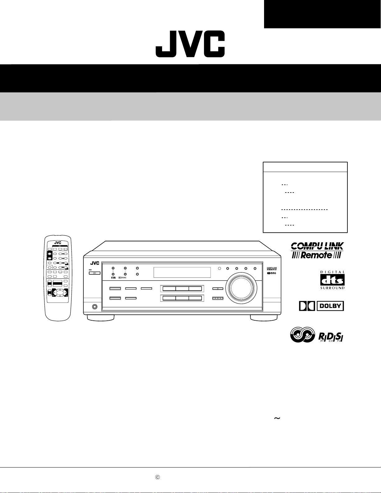
RX-6010RBK/RX-6012RSL
SERVICE MANUAL
AUDIO/VIDEO CONTROL RECEIVER
RX-6010RBK
TV
SLEEP
VCR
SURROUND
– SUBWOOFER +TEST
1
SURROUND
EFFECT
– CENTER +
MODE
54
5
– REAR•L + – VCR CH +
SOUND
7/P
TV/VIDEO CD-DISC
– REAR•R +
10
DVD
TV SOUND
VCR
CD
TAPE/CDR
+
+
TV VOL
VOLUME
–
–
£
PTY SEARCH
1
+
TV CH
–
7
DISPLAY
PTY –
RM-SRX6010R
REMOTE CONTROL
A/V CONTROL RECEIVER
AUDIO
5
5
ANALOG/DIGITAL
FM/AM
MUTING
RX-6012RSL
Area Suffix
RX-6010RBK
E
EN
Continental Europe
Northern Europe
RX-6010RSL
B
E
EN
32
6
5
98
MENU
+10
ENTER
8
1
+ PTY
PHONES
STANDBY
STANDBY/ON
FM/AM TUNING
DIGITAL
SURROUND
SURROUND ON/OFF
DSP MODE
FM/AM PRESET FM MODE
DIGITAL
INPUT ATT
SPEAKERS ON/OFF
MEMORY
INPUT DIGITALINPUT ANALOG
AUDIO/VIDEO CONTROL RECEIVER
DVD VCR TV SOUND
CD TAPE/CDR
SOURCE NAME
FM/AM
ADJUST
DOWN UP
CONTROL
EON
PTY SEARCH TA/NEWS/INFO
DISPLAY MODE
MASTER VOLUME
SETTING
Continental Europe
Northern Europe
DIGITAL
U.K.
As for RX-6012RSL the body is silver color
Contents
Safety precautions --------------------------------------------------------1-2
Disassembly method -----------------------------------------------------1-3
Adjustment method -------------------------------------------------------1-8
Description of major ICs -------------------------------------------------1-9 19
COPYRIGHT 2001 VICTOR COMPANY OF JAPAN, LTD.
No.20932
Apr. 2001
Page 2
RX-6010RBK/RX-6012RSL
1. This design of this product contains special hardware and many circuits and components specially for safety
purposes. For continued protection, no changes should be made to the original design unless authorized in
writing by the manufacturer. Replacement parts must be identical to those used in the original circuits. Services
should be performed by qualified personnel only.
2. Alterations of the design or circuitry of the product should not be made. Any design alterations of the product
should not be made. Any design alterations or additions will void the manufacturer`s warranty and will further
relieve the manufacture of responsibility for personal injury or property damage resulting therefrom.
3. Many electrical and mechanical parts in the products have special safety-related characteristics. These
characteristics are often not evident from visual inspection nor can the protection afforded by them necessarily
be obtained by using replacement components rated for higher voltage, wattage, etc. Replacement parts which
have these special safety characteristics are identified in the Parts List of Service Manual. Electrical
components having such features are identified by shading on the schematics and by ( ) on the Parts List in
the Service Manual. The use of a substitute replacement which does not have the same safety characteristics
as the recommended replacement parts shown in the Parts List of Service Manual may create shock, fire, or
other hazards.
4. The leads in the products are routed and dressed with ties, clamps, tubings, barriers and the like to be
separated from live parts, high temperature parts, moving parts and/or sharp edges for the prevention of
electric shock and fire hazard. When service is required, the original lead routing and dress should be
observed, and it should be confirmed that they have been returned to normal, after re-assembling.
5. Leakage currnet check (Electrical shock hazard testing)
After re-assembling the product, always perform an isolation check on the exposed metal parts of the product
(antenna terminals, knobs, metal cabinet, screw heads, headphone jack, control shafts, etc.) to be sure the
product is safe to operate without danger of electrical shock.
Do not use a line isolation transformer during this check.
Plug the AC line cord directly into the AC outlet. Using a "Leakage Current Tester", measure the leakage
current from each exposed metal parts of the cabinet, particularly any exposed metal part having a return
path to the chassis, to a known good earth ground. Any leakage current must not exceed 0.5mA AC (r.m.s.).
Alternate check method
Plug the AC line cord directly into the AC outlet. Use an AC voltmeter having, 1,000 ohms per volt or more
sensitivity in the following manner. Connect a 1,500 10W resistor paralleled by a 0.15 F AC-type capacitor
between an exposed metal part and a known good earth ground.
Measure the AC voltage across the resistor with the AC
voltmeter.
Move the resistor connection to eachexposed metal part,
particularly any exposed metal part having a return path to
the chassis, and meausre the AC voltage across the resistor.
Now, reverse the plug in the AC outlet and repeat each
measurement. voltage measured Any must not exceed 0.75 V
AC (r.m.s.). This corresponds to 0.5 mA AC (r.m.s.).
0.15 F AC TYPE
1500 10W
Good earth ground
AC VOLTMETER
(Having 1000
ohms/volts,
or more sensitivity)
Place this
probe on
each exposed
metal part.
!
1. This equipment has been designed and manufactured to meet international safety standards.
2. It is the legal responsibility of the repairer to ensure that these safety standards are maintained.
3. Repairs must be made in accordance with the relevant safety standards.
4. It is essential that safety critical components are replaced by approved parts.
5. If mains voltage selector is provided, check setting for local voltage.
Burrs formed during molding may
be left over on some parts of the
chassis. Therefore, pay attention to
such burrs in the case of
preforming repair of this system.
In regard with component parts appearing on the silk-screen printed side (parts side) of the PWB diagrams, the
parts that are printed over with black such as the resistor ( ), diode ( ) and ICP ( ) or identified by the " "
mark nearby are critical for safety.
When replacing them, be sure to use the parts of the same type and rating as specified by the manufacturer.
(Except the JC version)
1-2
Page 3
RX-6010RBK/RX-6012RSL
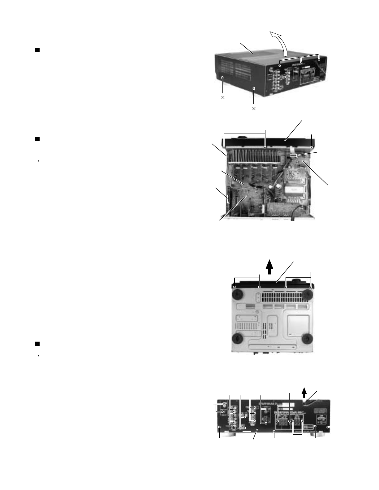
Disassembly method
Removing the top cover (See Fig.1)
1.
Remove the four screws A attaching the top cover
on both sides of the body.
2.
Remove the three screws B on the back of the body.
3.
Remove the top cover from behind in the direction of
the arrow while pulling both sides outward.
Removing the front panel assembly
(See Fig.2 and 3)
Prior to performing the following procedure, remove
the top cover.
1.
Disconnect the card wire from connector CN402 on
the audio board and CN201 on the power supply
board in the front panel assembly.
2.
Cut off the tie band fixing the harness.
Tie band
Main
board
CN402
Top cover
A
2
A
B
2
C
Fig.1
Front panel assembly
C
CN201
Power supply
board
3.
Remove the three screws C attaching the front
panel assembly.
4.
Remove the four screws D attaching the front panel
assembly on the bottom of the body. Detach the front
panel assembly toward the front.
Removing the rear panel (See Fig.4)
Prior to performing the following procedure, remove
the top cover.
1.
Remove the power cord stopper from the rear panel
by moving it in the direction of the arrow.
2.
Remove the seventeen screws E attaching the each
boards to the rear panel on the back of the body.
Audio board
E
E
E
E
D
E
Fig.2
Front panel assembly
Fig.3
E
D
Cord stopper
3.
Remove the four screws F attaching the rear panel
on the back of the body.
F
Rear panel
Fig.4
F
E
F
F
1-3
Page 4
RX-6010RBK/RX-6012RSL
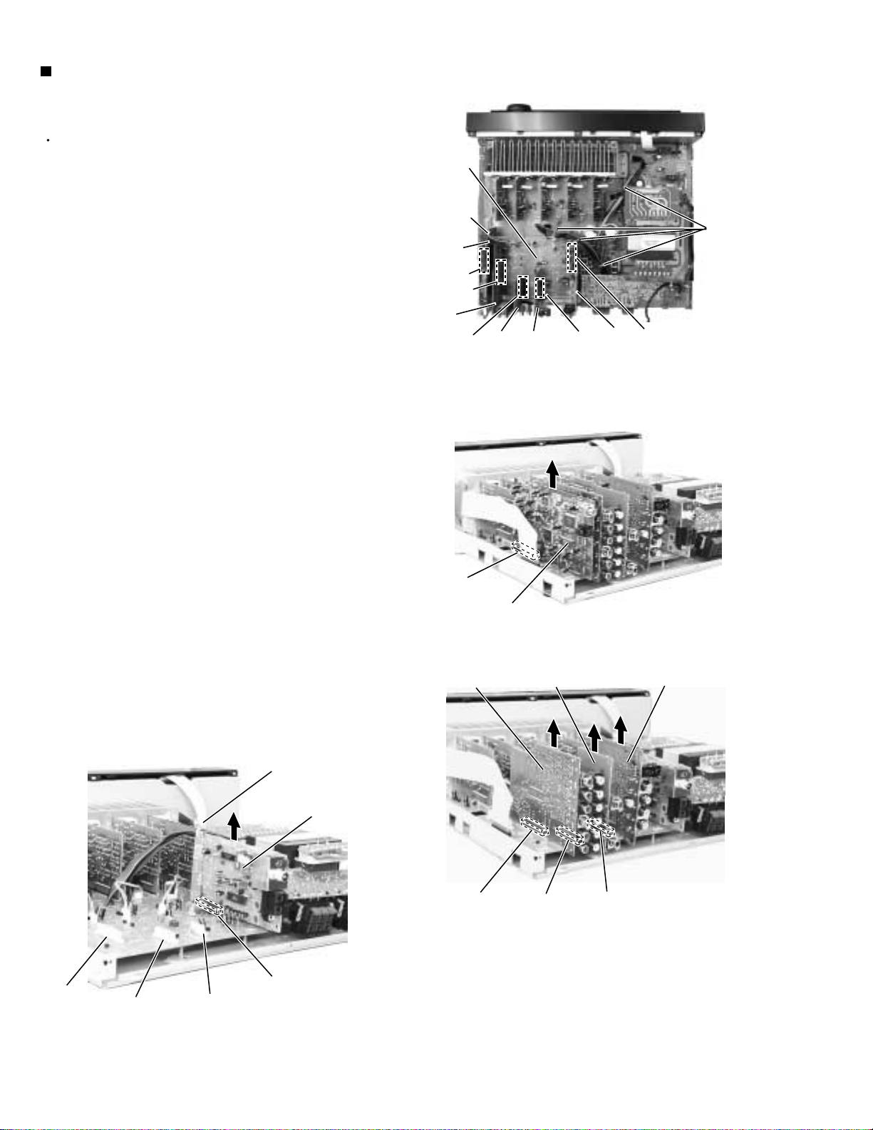
Removing each board connected to the
rear side of the audio board
(See Fig.5 to 8)
Prior to performing the following procedure, remove
the top cover and the rear panel.
1.
Cut off the tie band fixing the harness.
2.
Disconnect the DSP board from connector CN481 on
the audio board.
3.
Disconnect the audio input board. DVD board and
the video board from connector CN421, CN431 and
CN441 on the audio board.
4.
Disconnect the tuner board from connector CN411
and CN412 on the audio board.
Audio
board
Tie band
DSP
board
CN481
CN421
Audio
input
board
CN431
DVD
board
Video
board
CN441
Fig.5
Tuner
board
Tie band
CN411
CN412
CN421
CN431
CN441
Tie band
CN411
CN412
Tuner
board
CN481
DSP board
Audio
input
board
CN421
DVD
board
CN431
Fig.6
Video
board
CN441
Fig.7
1-4
Fig.8
Page 5

RX-6010RBK/RX-6012RSL
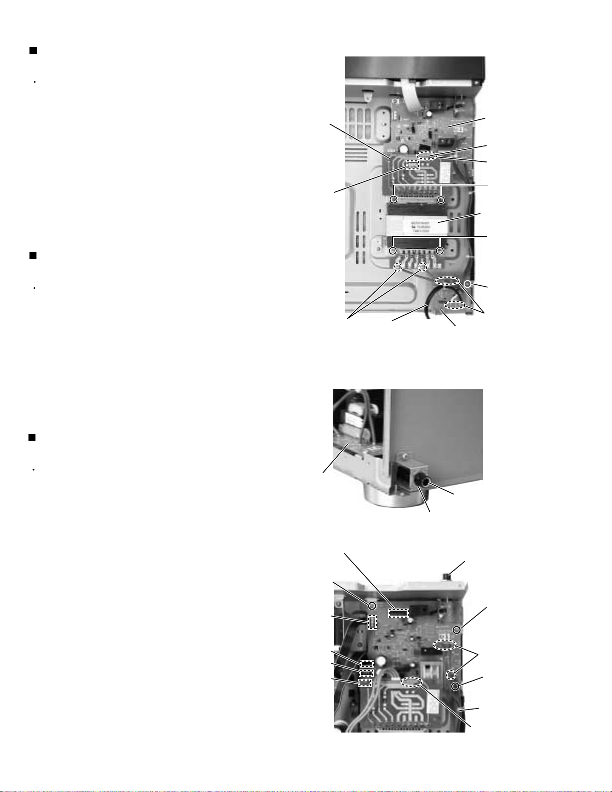
Removing the audio board
(See Fig.9)
Prior to performing the following procedure, remove
the top cover and the rear panel.
1.
Disconnect the card wire from connector CN402 on
the audio board.
2.
Disconnect the relay board from the audio board and
the power supply board. (CN291,CN491)
3.
Disconnect the harness from connector CN473,
CN471, CN472, CN403 and CN385.
4.
Remove the three screws G attaching the audio
board assembly.
5.
Remove the screw H attaching the audio board
assembly.
Removing the main board.
(See Fig.10)
Prior to performing the following procedure, remove
the top cover, the rear panel and audio board.
CN473
G
CN402
G
Audio board
CN471
I
J
I
CN472
CN403
CN385
G
Fig.9
I
Relay board
CN491
CN241
Power / Fuse
H
power
supply
board
CN291
Power
transformer
board
J
CN203
I
1.
Disconnect the harness from connector CN241 and
CN203 on the power supply board respectively.
2.
Remove the four screws I and the two screws J
attaching the main board.
Removing the Heat sink
(See Fig.11 to 12)
1.
Remove the ten screws K and four screws L
attaching the heat sink.
2.
Remove the two screws L' attaching the heat sink
from the rear side of main board.
Main
board
Heat sink
L
L'
K
Fig.10
Fig.11
K
K
L
L'
Main board
rear side
Fig.12
1-5
Page 6
RX-6010RBK/RX-6012RSL
Removing the power transformer
(See Fig.13)
Prior to performing the following procedures, remove
the top cover.
1.
Unsolder the two harnesses connected to the power
transformer.
2.
Disconnect the harness from connector CN251 and
unsolder the harnesses connected to FW201 on the
power transformer board.
3.
Remove the four screws M attaching the power
transformer.
Removing the power / fuse board
(See Fig.13)
Prior to performing the following procedure, remove
the top cover and the rear panel.
1.
Remove the screw N attaching the power / fuse
board.
Power
transformer
board
CN251
Solder
Power cord
Power
supply
board
FW201
Solder
M
Power
transformer
M
N
Solder
Power / fuse board
2.
Unsolder the power cord and other harnesses
connected to the power / fuse board.
Removing the power supply board
(See Fig.14 and 15)
Prior to performing the following procedure, remove
the top cover and the front panel.
1.
Remove the one nut attaching the headphone jack of
the power supply board on the front side of the body.
2.
Disconnect the harness connected to connector
CN241,CN201,CN203 and CN291 on the power
transformer board (If necessary, cut off the band
fixing the harness on the side of the base chassis).
3.
Remove the three screws O attaching the power
supply board and pull out the power supply board
from the front bracket backward.
Power
supply
board
CN201
O
CN241
Fig.13
Headphone jack
Nut
Fig.14
Headphone jack
O
4.
Unsolder the three harnesses connected to the
power supply board.
1-6
CN203
CN291
Hook
Solder
O
Tie band
Solder
Fig.15
Page 7

RX-6010RBK/RX-6012RSL
Removing the system control board /
power switch board (See Fig.16 to 18)
Prior to performing the following procedure, remove
the top cover and the front panel assembly.
1.
Pull out the volume knob on the front side of the front
panel and remove the nut attaching the system
control board.
2.
Remove the two screws P attaching the power
switch board.
3.
Disconnect the harness from connector CN714 on
the power switch board.
4.
Remove the six screws Q attaching the system
control board on the back of the front panel.
5.
On the back of the front panel, release the eight
joints by pushing the joint tabs inward.
Remove the operation switch panel toward the front.
6.
Release the two hook attaching the system control
board.
Operation switch panel
Fig.16
Q
Joint
Joint
Q
Nut
Joint
Front panel assembly
Volume knob
Power switch
board
Joint
P
Joint
Joint
Hook
Joint
Fig.17
System control board
Fig.18
Hook
Joint
CN714
1-7
Page 8

RX-6010RBK/RX-6012RSL
Adjustment method
Tuner section
1.Tuner range
FM 87.5MHz~108.0MHz
AM (MW) 522kHz~1629kHz
(LW) 144kHz~ 288kHz
Power amplifier section
Adjustment of idling current
Measurement location TP301(Lch) , TP302(Rch)
Adjustment part VR301(Lch) , VR302(Rch)
Attention
This adjustment does not obtain a correct adjustment value immediately after the amplifier is
used (state that an internal temperature has risen).
Please adjust immediately after using the amplifier after turning off the power supply of the
amplifier and falling an internal temperature.
<Adjustment method>
1.Set the volume control to minimum during this adjustment.(No signal & No load)
2.Set the surround mode OFF.
2.Turn VR301 and VR302 fully counterclockwise to warm up before adjustment.
If the heat sink is already warm from previous use the correct adjustment can not be made.
3.For L-ch,connect a DC voltmeter between TP301's B216 and B217 (Lch)
And,connect it between TP302's B218 and B219(Rch).
4.30 minutes later after power on, adjust VR301 for L-ch, or VR302 for R-ch so that the DC voltmeter
value has 1mV~10mV.
* It is not abnormal though the idling current might not become 0mA even if it is finished to turn variable
resistance (VR301,VR302) in the direction of counterclockwise.
TP302(Rch)
VR302 (Rch)
1-8
VR301 (Lch)
TP301(Lch)
Heat sink
Page 9

Description of major ICs
SAA6588 (IC191) : RDS detector
RX-6010RBK/RX-6012RSL
1.Terminal Layout
NC
SDA
SCL
1
2
3
4
5
6
7
8
9
10
MRO
GND
OSCO
OSCI
VSSD
VDDD
DAVN
20
19
18
17
16
15
14
13
12
11
NC
CIN
SCOUT
Vref
MPX
VSSA
VDDA
NC
GND
NC
2.Pin Function
Pin
No.
1
2
3
4
5
6
7
8
9
10
11
12
13
14
15
16
17
18
19
20
MRO
NC
GND
OSCO
OSCI
VSSD
VDDD
DAVN
SDA
SCL
NC
GND
NC
VDDA
VSSA
MPX
Vref
SCOUT
CIN
NC
FunctionI/OSymbol
O
Multi-path rectifier output
-
Non connect
I
Test control input pin
O
Oscillator output
I
Oscillator input
-
Digital ground (0V)
-
Digital power supply (5V)
O
Data available output (active LOW)
I/O
IC-bus serial data I/O
I
IC-bus serial clock input
-
Non connect
-
Connect to ground
-
Non connect
-
Analog power supply (5V)
Connect to ground
-
Multiplex input signal
I
Reference voltage output
O
Band-pass filter output
O
Comparator output
O
Level input
I
3.Block Diagram
16
MPX
13
AFIN
LVIN
20
VDDA
14
8th ORDER
BAND-PASS
DETECTOR
AND RESET
VSSA
SCOUT
57 kHz
PAUSE
POWER
SUPPLY
15
18
17
Vref
19
CLOCK
COMPARATOR
MULTI-PATH
DETECTOR
TEST
CONTROL
3
TCON
RDS/RDBS
DEMODULATOR
SIGNAL QUALITY
DETECTOR
OSCILLATOR
AND CLOCK
1
MRO
OSCI OSCO
VDDDCIN
7
DAVN
12
MAD
11
10
8
2
9
PSWN
MPTH
SDA
SCL
RDS/RDBS
DECODER
INTERFACE
REGISTER
IC-BUS SLAVE
TRANSCEIVER
5
4
6
VSSD
1-9
Page 10

RX-6010RBK/RX-6012RSL
AK4527B (IC601) : A/D,D/A converter
1.Pin layout
LOOP1
LOOP0/SDA/CDTI
DIF1/SCL/CCLK
DIF0/CSN
P/S
MCLK
DZF1
AVSS
AVDD
VREFH
VCOM
SDOS
I2C
SMUTE
BICK
LRCK
SDTI1
SDTI2
SDTI3
SDTO
DAUX
DFS
2. Pin function (1/2)
No.
1
2
3
4
5
6
7
8
9
10
11
12
13
14
15
16
17
18
Pin name
SDOS
I2C
SMUTE
BICK
LRCK
SDTI1
SDTI2
SDTI3
SDTO
DAUX
DFS
NC
DZEF
TVDD
DVDD
DVSS
PDN
TST
4443424140393837363534
1
2
3
4
5
6
7
8
9
10
11
I/O
I
SDTO Source Select Pin (Note 1)
AK4527BVQ
Top View
1213141516171819202122
NC
DZFE
TVDD
DVDD
DVSS
PDN
TSTNCADIF
Function
CAD1
CAD0
33
32
31
30
29
28
27
26
25
24
23
DZF2/OVF
RIN+
RINLIN+
LINROUT1
LOUT1
ROUT2
LOUT2
ROUT3
LOUT3
"L" : Internal ADC output, "H" : DAUX input
I
Control Mode Select Pin
"L" : 3-wire Serial, "H" : I
I
Soft Mute Pin (Note 1)
2
C Bus
When this pin goes to "H", soft mute cycle is initialized.
When returning to "L", the output mute releases.
I
Audio Serial Data Clock Pin
I/O
Input Channel Clock Pin
I
DAC1 Audio Serial Data Input Pin
I
DAC2 Audio Serial Data Input Pin
I
DAC3 Audio Serial Data Input Pin
O
Audio Serial Data Output Pin
I
Sub Audio Serial Data Input Pin
I
Double Speed Sampling Mode Pin (Note 1)
"L" : Normal Speed, "H" : Double Speed
-
No Connect
No internal bonding.
I
Zero Input Detect Enable Pin
"L" : mode 7 (disable) at parallel mode,
zero detect mode is selectable by DZFM2-0 bits at serial mode.
"H" : mode 0 (DZF is AND of all six channels)
-
Output Buffer Power supply Pin, 2.7V~5.5V
-
Digital Power Supply Pin, 4.5V~5.5V
-
De-emphasis Pin, 0V
I
Power-Down & Reset Pin
When "L", the AK4527B is powered-down and the control registers are reset to default
state. If the state of P/S or CAD0-1 changes, then the AK4527B must be reset by PDN.
I
Test Pin
This pin should be connected to DVSS.
AK4527(1/2)
1-10
Page 11

RX-6010RBK/RX-6012RSL
Pin function (2/2)
Pin name
No.
NC
19
ADIF
20
CAD1
21
CAD0
22
LOUT3
23
ROUT3
24
LOUT2
25
ROUT2
26
LOUT1
27
ROUT1
28
LIN-
29
LIN+
30
RIN-
31
RIN+
32
DZF2
33
OVF
VCOM
34
VREFH
35
AVDD
36
AVSS
37
DZF1
38
MCLK
39
P/S
40
DIF0
41
CSN
DIF1
42
SCL/CCLK
LOOP0
43
SAD/CDTI
LOOP1
44
No Connect
I/O
No internal bonding.
Analog Input Format Select Pin
"H" : Full-differential input, "L" : Single-ended input
I
Chip Address 1 Pin
Chip Address 0 Pin
I
DAC3 Lch Analog Output Pin
I
DAC3 Rch Analog Output Pin
O
DAC2 Lch Analog Output Pin
O
DAC2 Rch Analog Output Pin
O
DAC1 Lch Analog Output Pin
O
DAC1 Rch Analog Output Pin
O
Lch Analog Negative Input Pin
O
Lch Analog Positive Input Pin
I
Rch Analog Negative Input Pin
I
Rch Analog Positive Input Pin
I
Zero Input Detect 2 Pin (Note 2)
I
When the input data of the group 1 follow total 8192LRCK cycles with "0" input data,
O
this pin goes to "H".
Analog Input Overflow Detect Pin (Note 3)
This pin goes to "H" if the analog input of Lch or Rch is overflows.
O
Common Voltage Output Pin,AVDD/2
Large external capacitor around 2.2uF is used to reduce power-supply noise.
O
Positive Voltage Reference Input Pin,AVDD
Analog Power Supply Pin,4.5V~5.5V
I
Analog Ground Pin,0V
Zero Input Detect 1 Pin (Note 2)
When the input data of the group 1 follow total 8192 LRCK cycles with "0" input data,
O
this pin goes to "H".
Master Clock Input Pin
Parallel / Serial Select Pin
I
"L" : Serial control mode, "H" : Parallel control mode
I
Audio Data Interface Format 0 Pin in parallel mode
Chip select pin in 3-wire serial control mode
I
This pin should be connected to DVDD at I2C bus control mode
I
Audio Data Interface Format 1 Pin in parallel mode
Control Data Clock Pin in serial control mode
I
I2C = "L" : CCLK(3-wire Serial), I2C = "H" : SCL(I2CBus)
I
Loopback Mode 0 Pin in parallel control mode
Enables digital loop-back from ADC to 3 DACs.
I
Control Data Input Pin in serial control mode
I2C = "L" : CDTI(3-wire Serial), I2C = "H" : SDA(I2CBus)
I/O
Loopback Mode 1 Pin (Note 1)
Enable all 3 DAC channels to be input from SDTII.
I
Function
AK4527(1/2)
Notes : 1. SDOS, SMUTE, DFS, and LOOP1 pins are ORed with register data if P/S = "L".
2. The group 1 and 2 can be selected by DZFM2-0 bit if P/S = "L" and DZFME = "L".
3. This pin becomes OVF pin if OVFE bit is set to "1" at serial control mode.
4. All input pins should not be left floating.
1-11
Page 12

RX-6010RBK/RX-6012RSL
TC9164AN (IC402) : Analog switch
1.Function
Switch to On/Off of S1 to S8 by control of LSI.
2.Terminal Lay out & Block Diagram
TC9164AN
VSS
L-S1
S-2
S-3
S-4
COM-1
S-5
S-6
COM-2
S-7
S-8
COM3
ST
GND
1
2
3
4
SHIFT
5
RESISTOR
6
7
8
9
10
11
12
13
14
&
LATCH
SHIFT RESISTOR
SHIFT
RESISTOR
&
LATCH
28
27
26
25
24
23
22
21
20
19
18
17
16
15
VDD
R-S1
S-2
S-3
S-4
COM-1
S-5
S-6
COM-2
S-7
S-8
COM3
DATA
CK
NJM2246D (IC501) : Video switch
GND
8
Vout
7
V+
6
Vin3
5
1
Vin1
6dB
AMP.
2
CTL1
3
Vin2
BIAS
4
CTL2
Control input - output signal
CTL 1
L
H
L/H
CTL 2
L
L
H
Output
VIN 1
VIN 2
VIN 3
1-12
Page 13

W24L010AJ-12 (IC641) : CMOS SRAM
RX-6010RBK/RX-6012RSL
Block diagram
A16
A14
A12
A4
A3
A2
A7
A6
A5
A9
I/O 1
I/O8
WE
CS1
CS2
R
O
W
D
E
C
O
D
E
R
DATA
CNTRL.
CLK
GEN.
PRECHARGE CKT.CLK GEN.
CORE CELL ARRAY
7024 ROWS
728x8 COLUMN5
I/O CKT
COLUMN DECODER
A15 A13 A8 A1 A0 A11 A10
Pin layout
NC
A16
A14
A12
A7
A6
A5
A4
A3
A2
A1
A0
I/O1
I/O2
I/O3
Vss
1
2
3
4
5
6
7
8
9
10
11
12
13
14
15
16
32
31
30
29
28
27
26
25
24
23
22
21
20
19
18
17
VDD
A15
CS2
WE
A13
A8
A9
A11
OE
A10
CS2
I/O8
I/O7
I/O6
I/O5
I/O4
OE
PQ3DZ53 (IC681) : Regulator IC
DC INPUT(Vin)
1
CUSTOM IC
5
GND
RN5RZ33BA (IC683) : Voltage regurator
2
VDD
-
+
3
DC OUTPUT(Vo)
ON/OFF CONTROL(Vc)
2
VOUT
3
CE
Vref
GND
Current Limit
5
1
1-13
Page 14

RX-6010RBK/RX-6012RSL
M62446FP (IC428) : 6CH master volume
1.Block Diagram
OUT4
OUT3
OUT2
OUT1
AVDD
SWIN
GNDS
SRin
SLin
GNDC
Cin
GNDR
Rin
GNDL
Lin
BYPASSR
BYPASSL
LTRE
LBASS3
LBASS2
LBASS1
10
11
12
13
14
15
16
17
18
19
20
21
1
2
3
4
5
6
7
8
9
OUTPUT
PORT
tone
volume
volume
volume
volume
volume
volume
MCU
I/F
tone
42
41
40
39
38
37
36
35
34
33
32
31
30
29
28
27
26
25
24
23
22
DVDD
CLK
D ATA
LATCH
DGND
AGND
SWout
SRout
SLout
Cout
Rout
Lout
AVSS
CL1
CL2
CR1
CR2
RTRE
RBASS3
RBASS2
RBASS1
1-14
Page 15

2.Pin Function
RX-6010RBK/RX-6012RSL
Pin No.
1
2
3
4
5
6
7
8
9
10
11
12
13
14
15
16,17
18
19~21
22
23,24
25
26
27
28
29
30
31
32
33
34
35
36
37
38
39
40
41
42
Symbol I/O Descriptions
SURROUND
BASS BOOST
INPUT-ATT
MUTING
AVDD
SWIN
A.GND
RR IN
RL IN
A.GND
C IN
A.GND
R IN
A.GND
L IN
BYPASSR,L
LTRE
LBASS3~1
CR2
RBASS2,4
RTRE
RBASS1
CR1
CL2
CL1
AVSS
L OUT
R OUT
C OUT
RL OUT
RR OUT
SW OUT
A.GND
D.GND
VOL STB
VOL DATA
VOL CLK
DVDD
O
O
O
O
I
I
I
I
I
I
-
-
-
O
-
-
I
O
I
O
O
O
O
O
O
-
-
I
I
I
-
SURROUND control terminal
BASS BOOST control terminal
Input attenuator control terminal
MUTING control terminal
Analog positive power supply terminal
SUB Woofer volume signal input terminal
Analog ground terminal
R ch volume signal input terminal for rear speaker
L ch volume signal input terminal for rear speaker
Analog ground terminal
Center volume signal input terminal
Analog ground terminal
R ch volume signal input terminal
Analog ground terminal
L ch volume signal input terminal
Non connect
Frequency adjustment terminal tone/treble
Frequency adjustment terminal tone/bass
Tone output terminal
Frequency adjustment terminal tone/bass
Frequency adjustment terminal tone/treble
Frequency adjustment terminal tone/bass
L/R volume input terminal
Tone output terminal
L/R volume input terminal
Analog negative power supply terminal
L ch output
R ch output
Center volume signal output terminal
L ch volume signal output terminal for rear speaker
R ch volume signal output terminal for rear speaker
SUB Woofer volume signal output terminal
Analog ground terminal
Digital ground terminal
Latch input terminal
Volume data input terminal
Clock input terminal for data transfer
Digital power supply terminal
1-15
Page 16

RX-6010RBK/RX-6012RSL
MN101C35DHK1 (IC701) : System controller
100 76
1
75
Pin function (1/2)
Pin No.
1
2
TXD/SB00/P00
RXD/SBI0/P01
3
4
5
6
7
BUZZER/P06
8
9,10
11
12
13
14
15
16
17
18
19
20
21
22
23
24
25
26
27
RNOUT/TM0I0/P10
28
29
30
31
32
33
34
SENS/IRQ1/P21
35
36
37
38
39
40
25
Symbol
SBT0/P02
SB01/P03
SBI1/P04
SBT1/P05
VDD
OSC1,2
VSS
XI
X0
MMOD
VREFAN0/PA0
AN1/PA1
AN2/PA2
AN3/PA3
AN4/PA4
AN5/PA5
AN5/PA5
AN5/PA5
VREF+
P07
RST /P27
TM1I0/P11
TM2I0/P12
TM3I0/P13
TM4I0/P14
P15
IRQ0/P20
IRQ2/P22
IRQ3/P23
IRQ4/P24
P25
SB02/P30
SBI2/P31
26 50
51
I/O
I
I
I/O
O
O
I
I
-
I/O
I
O
I
I
I
I
I
I
I
I
I
I
I
O
I
O
I
O
I/O
I
I
I
I
I
I
O
I
Function
VOL.JOG IN_1
VOL.JOG IN_2
DATA (PLL)
CLK (PLL)
CE (PLL)
VIDEO S/C DVD
VIDEO S/C VCR
Power supply +5V
OSC (8MHz)
GND
GND
OPEN
GND
GND
KEY INPUT 1 (7KEY)
KEY INPUT 2 (7KEY)
KEY INPUT 3 (7KEY)
KEY INPUT 4 (7KEY)
KEY INPUT 5 (7KEY)
INH IN
CHIP SELECT 1
CHIP SELECT 2
Power supply +5V
VIDEO S/C DBS
RESET INPUT
RDS CLK OUT (RDS)
DCS INPUT
DCS OUTPUT
AVLINK VCR IN
AVLINK VCR OUT
RDS DATA (RDS)
PROTECTOR IN
REMOCON INPUT
TUNED IN (TUNER)
STEREO IN (TUNER)
RDS DAVN (RDS)
SELF CHECK INPUT
COMMAND (DSP)
STATUS (DSP)
1-16
Page 17

Pin function (2/2)
RX-6010RBK/RX-6012RSL
Pin No.
41
42
43
44
45
46
47
48
49 64
65 80
81
82
83
84
85
86
87
88
89
90
91
92
93
94
95
96
97
98
99
100
Symbol
SBT2/P32
P50
P51
P52
P53
P54
DGT17/P67
DGT16/P66
G16 G1
P87 P90
SEG24/PC2
SEG25/PC1
SEG26/PC0
SEG27/PB7
SEG28/PB6
SEG29/PB5
SEG30/PB4
SEG31/PB3
SEG32/PB2
SEG33/PB1
SEG34/PB0
SEG35/PD7
SEG36/PD6
SEG37/PD5
SEG38/PD4
SEG39/PD3
SEG40/PD2
SEG41/PD1
SEG42/PD0
VPP
I/O
O
O
O
O
O
O
O
O
O
O
-
-
-
-
-
-
-
O
O
O
O
O
O
O
O
O
O
O
O
Function
CLK (DSP)
READY (DSP)
RESET (DSP)
RELAY S
RELAY C
RELAY L/R 1
RELAY L/R 2
RELAY HEADPHONE
FL GRID SIGNAL CONTROL OUT
FL SEGMENT SIGNAL CONTROL OUT
No Connect
No Connect
No Connect
No Connect
No Connect
No Connect
No Connect
No Connect
SOUSE MUTE
SUBWOOFER MUTE
TUNER MUTE
POWER ON (STANDBY)
SURROUND
DATA (A.SW)
CLK (A.SW)
STB (A.SW)
LATCH (VOL)
DATA (VOL)
CLK (VOL)
VPP
1-17
Page 18

RX-6010RBK/RX-6012RSL
TC9446F-014 (IC631) : Digital signal processor for dolby digital (AC-3)
/ MPEG2 audio decode
Pin No. Symbol I/O Function
1
2
3
4
5
6
7
8~11
12
13
14
15
16~18
19
20
21
22
23
24
25
26
27,28
29~31
32,33
34
35
36
37
38,39
40
41
42
43
44
45
46
47
48
49
50
51
52
53
54~61
62
63~70
71
72~80
81
82~89
90
91
92,93
94
95
96
97
98,99
100
RST
MIMD
MICS
MILP
MIDIO
MICK
MIACK
FI0~3
IRQ
VSS
LRCKA
BCKA
SDO0~2
SD03
LRCKB
BCKB
SDT0
SDT1
VDD
LRCKOA
BCKOA
TEST0,1
LRCKOB,BCKOB,TXO
TEST2,3
RX
VSS
TSTSUB0
FCONT
TSTSUB1,TSTSUB2
PDO
VDDA
PLON
AMPI
AMPO
CKI
VSSA
CKO
LOCK
VSS
WR
OE
CE
VDD
IO7~0
VSS
AD0~7
VDD
AD8~16
VSS
PO0~7
VDDDL
LPFO
DLON,DLCKS
SCKO
VSSDL
SCKI
VSSX
XO,XI
VDDX
Reset signal input terminal (L:reset H:Operation usually)
I
Microcomputer interface mode selection input terminal (L:serial H:IC bus)
I
Microcomputer interface chip select input terminal
I
Microcomputer interface latch pulse input
I
Microcomputer interface data I/O terminal
I/O
Microcomputer interface clock input terminal
I
Microcomputer interface acknowledge output terminal
O
Flag input terminal 0~3
I
Interrupt input terminal
I
Digital ground terminal
Audio interface LR clock input terminal A
I
Audio interface bit clock input terminal A
I
Audio interface data output terminal 0
O
Non connect
Audio interface LR clock input terminal B
I
Audio interface bit clock input terminal B
I
Audio interface data input terminal 0
I
Audio interface data input terminal 1
I
Power supply for digital circuit
Audio interface LR clock output terminal A
O
Audio interface bit clock output terminal A
O
Test input terminal 0/1 (L:test H:operation usually)
I
Non connect
Test input terminal (L:test H:operation usually)
I
SPDIF input terminal
I
Ground terminal for digital circuit
Test sub input terminal 0 (L:test H:operation usually)
I
VCO Frequency control output terminal
O
Test sub input terminal 1,2 (L:test H:operation usually)
I
Phase error signal output terminal
O
Power supply for analog circuit
Clock selection input terminal (L:external clock H:VCO clock)
I
AMP.input terminal for LPF
I
AMP.output terminal for LPF
O
External clock input terminal
I
Ground terminal for analog circuit
DIR Clock output terminal
O
VCO Lock detection output terminal
O
Ground terminal for digital circuit
External SRAM writing signal output terminal
O
External SRAM output enable signal output terminal
O
External SRAM chip enable signal output terminal
O
Power supply terminal for digital circuit
External SRAM data I/O terminal 7~0
I/O
Ground terminal for digital circuit
External SRAM address output terminal 0~7
O
Power supply terminal for digital circuit
External SRAM address output terminal 8~16
O
Ground terminal for digital circuit
General purpose output terminal 0~7
O
Power supply terminal for DLL
LPF output terminal for DLL
O
Refer to the undermentioned table
I
Non connect
Ground terminal for DLL
External system clock input terminal
I
Ground termonal for oscillation circuit
Oscillation I/O terminal
I/O
Power supply terminal for oscillation circuit
-
1-18
DLCKS terminal
L
L
H
H
DLONterminal
L
H
L
H
DLL clock setting
SCKI input (DLL circuit OFF)
Four times XI clock
Three times XI clock
Six times XI clock
Page 19

UPD784215AGC103 (IC671) : UNIT CPU
1.Pin layout
75 ~ 51
76
~
50
~
RX-6010RBK/RX-6012RSL
100
1 ~ 25
26
2.Pin function
Pin No. Symbol I/O Function
1~8
9
10
11
12
13
14
15
16
17
18
19
20
21
22
23
24
25~32
33
34,35
36
37,38
39
40
41
42
43
44
45,46
47
48
49
50
51,52
53
54~63
64,65
66
67
68
69,70
71
72
73~80
81
82
83
84
85
86
87
88
89
90~93
94
95~100
VDD
X2
X1
VSS
XT2
XT1
RESET
AUTODATA
LOCK
DIGITAL0
FORMAT
CHANNEL
ERR
RSTDET
AVDD
AVREF0
AVSS
AV REF1
RX,TX
DSPCOM
DSPSTS
DSPCLK
DSPRDY
MIDIO_IN/OUT
MICK
MICS
MILP
MIACK
DSPRST
CDTI/CDTO
CCLK
CS
XTS
PD
GND
VDD
3D-ON
3D-ON
ANA/T-TONE
REF-MIX
D.MUTE
S.MUTE
ASW1~4
TEST
Non connect
Power supply terminal
Connecting the crystal oscillator for system main clock
O
Connecting the crystal oscillator for system main clock
I
Connect to GND
Connecting the crystal oscillator for system sub clock
O
Connecting the crystal oscillator for system sub clock
I
System reset signal input
I
Output of DSP to general-purpose port
I
Output of DSP to general-purpose port
I
Output of DSP to general-purpose port
I
Output of DSP to general-purpose port
I
Output of DSP to general-purpose port
I
Output of DSP to general-purpose port
I
Reset signal input
I
Power supply terminal
Connect to GND
Connect to GND
Connect to GND
Non connect
Power supply terminal
Not use
Non connect
Communication port from IC701
I
Status communication port to IC701
O
Clock input from IC701
I
Ready signal input from IC701
I
Non connect
Interface I/O terminal with microcomputer
I/O
Interface I/O terminal with microcomputer of clock signal
O
Interface I/O terminal with microcomputer of chip select
O
Interface I/O termonal with microcomputer
O
Interface I/O termonal with microcomputer
O
Non connect
Reset signal output of DSP
O
Non connect
Interface I/O terminal with microcomputer
I/O
Interface I/O terminal with microcomputer of clock signal
O
Interface I/O terminal with microcomputer of chip select
O
OSC Select
O
Non connect
Reset signal output
O
Connect to GND
Non connect
Power supply
Non connect
Switch at output destination of surround channel
O
Test tone control
O
Control at output destination of LFE channel
O
Non connect
Mute of the digital out terminal is controlled
O
Mute of the audio signal is controlled
O
Non connect
Selection of digital input selector
O
Test terminal
Non connect
-
1-19
Page 20

RX-6010RBK/RX-6012RSL
VICTOR COMPANY OF JAPAN, LIMITED
AUDIO & COMMUNICATION BUSINESS DIVISION
PERSONAL & MOBILE NETWORK BUSINESS UNIT. 10-1,1chome,Ohwatari-machi,Maebashi-city,371-8543,Japan
(No.20932)
Printed in Japan
200104(V)
 Loading...