

Page 1
SERVICE MANUAL
AUDIO/VIDEO CONTROL RECEIVER
2203820034
RX-5032VSL
MASTER VOLUME
DIMMER
INPUT ATT
TA/NEWS/INFO
DISPLAY MODE
RXÐ6030V
STANDBY
STANDBY/ON
PHONES
DIGITAL
PRO LOGIC
AUDIO/VIDEO CONTROL RECEIVER
INPUT DIGITAL
INPUT ANALOG
Area Suffix
E ----- Continental Europe
EN ----- Northern Europe
TABLE OF CONTENTS
1 Important Safety Precautions . . . . . . . . . . . . . . . . . . . . . . . . . . . . . . . . . . . . . . . . . . . . . . . . . . . . . . . . . . . 1-2
2 Disassembly method . . . . . . . . . . . . . . . . . . . . . . . . . . . . . . . . . . . . . . . . . . . . . . . . . . . . . . . . . . . . . . . . . . 1-3
3 Adjustment. . . . . . . . . . . . . . . . . . . . . . . . . . . . . . . . . . . . . . . . . . . . . . . . . . . . . . . . . . . . . . . . . . . . . . . . . . 1-10
4 Description of major ICs. . . . . . . . . . . . . . . . . . . . . . . . . . . . . . . . . . . . . . . . . . . . . . . . . . . . . . . . . . . . . . . 1-11
COPYRIGHT © 2003 VICTOR COMPANY OF JAPAN, LTD.
No.22038
2003/4
Page 2

SECTION 1
Important Safety Precautions
1.1 Safety Precautions
(1) This d esign of this product co ntains special hardware and
many circuits and components specially for safety purposes.
For continued protection, no changes should be made to the
original design unless authorized in writing by the manufacturer. Replacement parts must be identical to those
used in the original circuits. Services should be performed by qualified personnel only.
(2) Alterations o f the design or circuitry of the p roduct should
not be made. Any design alterations of the product should
not be made. Any design alterations or additions will void
the manufacturers warranty and will further relieve the
manufacture of responsibility for personal injury or property
damage resulting therefrom.
(3) Many electrical and mechanical parts in the products have
special safety-related characteristics. These characteristics are often not evident from visual inspection nor can the
protection afforded by them necessarily be obtained by using replacement components rated for higher voltage, watt age, etc. Replacement parts which have these special safety
characteristics are identified in the Parts List of Service Manual. Electrical components having such feat ures are id en tified by shading on the schematics and by ( ) on the
Parts List in the Service Manual. The use of a substitute replacement which does not have the same safety characteristics as the recommended replacement parts shown in the
Parts List of Service Manual may create shock, fire, or other hazards.
(4) The leads in the products are routed and dressed with ties,
clamps, tubings, barriers and the like to be separated from
live parts, high temperature parts, moving parts and/or
sharp edges for the prevention of electric shock and fire
hazard. When service is required, the origin al lead routing
and dress should be observed, and it should be confirmed
that they have been returned to normal, after reassembling.
(5) Leakage shock hazard testing)
After reassembling the product, always perform an isolation
check on the exposed metal parts of the product (antenna
terminals, knobs, metal cabinet, screw heads, headphone
jack, control shafts, etc.) to be sure the product is safe to
operate without danger of electrical shock.
Do not use a line isolation transformer during this check.
• Plug the AC line cord directly into the AC outlet. Using a
"Leakage Current Tester", measure the leakage current
from each exposed metal parts of the cabinet, particularly any exposed metal part having a return path to the
chassis, to a known good earth ground. Any leakage current must not exceed 0.5mA AC (r.m.s.).
• Alternate check method
Plug the AC line cord directly into the AC outlet. Use an AC
voltmeter having, 1,000 ohms per volt or more sensitivity in
the following manner. Connect a 1,500 ohm 10W resistor
paralleled by a 0.15 µF AC-type capacitor between an
exposed metal part and a known good earth ground.
Measure the AC voltage across the resistor with the AC
voltmeter.
Move the resistor connection to each exposed metal part,
particularly any exposed metal part having a return path to
the chassis, and measure the AC voltage across the resistor.
Now, reverse the plug in the AC outlet and repeat each
measurement. Voltage measured any must not exceed 0.75
V AC (r.m.s.). This corresponds to 0.5 mA AC (r.m.s.).
1.2 Warning
(1) This equipment has been designed and manufactured to
meet international safety standards.
(2) It is the leg al responsibility of the repairer to ensure that
these safety standards are maintained.
(3) Repairs must be made in accordance with the relevant
safety standards.
(4) It is essential that safety critical components a re replaced
by approved parts.
(5) If mains voltage selector is provided, check setting for local
voltage.
1.3 Caution Burrs formed during molding may be left over on some parts
of the chassis.
Therefore, pay attention to such burrs in the case of preforming repair of this system.
1.4 Critical parts for safety
In regard with component parts appearing on the silk-screen
printed side (parts side) of the PWB diagrams, the parts that are
printed over with black such as the resistor ( ), diode ( )
and ICP ( ) or identified by the " " mark nearby are critical
for safety.
When replacing them, be sure to use the parts o f the same type
and rating as specified by the manufacturer. (Except the JC version)
1-2 (No.22038)
Page 3
SECTION 2
y
Disassembly method
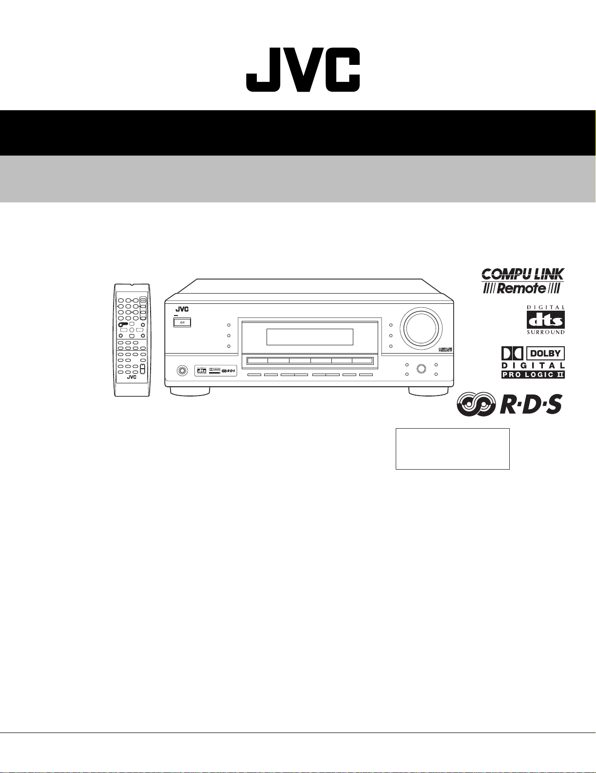
2.1 Removing the top cover
(See Fig.1)
(1) From the righ t and left sid es of the main body, remove the
four screws A attaching the top cover.
(2) From the back side of the main body, remove the three
screws B attaching the top cover.
(3) Remove th e top cover in the direction of the arrow 2 whi le
extending the lower sections of the top cover in the direction of the arrow 1.
Top cover
2
B
1
2.2 Removing the front panel assembly
(See Figs.2 and 3)
• Prior to performing the following procedure, re move the top
cover.
(1) Disconnect the card wire from the connector CN402 on the
audio board. (See Fig.2)
(2) Disconnect the card wire from the connector CN201 on the
power supply board. (See Fig.2)
(3) Remove the tie band and wire protection board fixing the
card wire. (See Fig.2)
(4) Remove the tie band fixing the parallel wires, disconnect
the parallel wire from the connector CN403 on the audio
board. (See Fig.2)
(5) Remove the three screws C attaching the front panel as-
sembly. (See Fig.2)
(6) From the b ottom side of the main body, remove the four
screws D attaching the front panel assembly. (See Fig.3)
(7) Remove the front panel assembly in the direction of the ar-
row. (See Fig.3)
1
A
A
Fig.1
Front panel assembly
C C C
Tie band
Wire protection
board
Card wire
CN402
Audio board
Card wire
CN201
Power suppl
board
Tie band
CN403
Fig.2
Front panel assembly
DD
Fig.3
(No.22038)1-3
Page 4
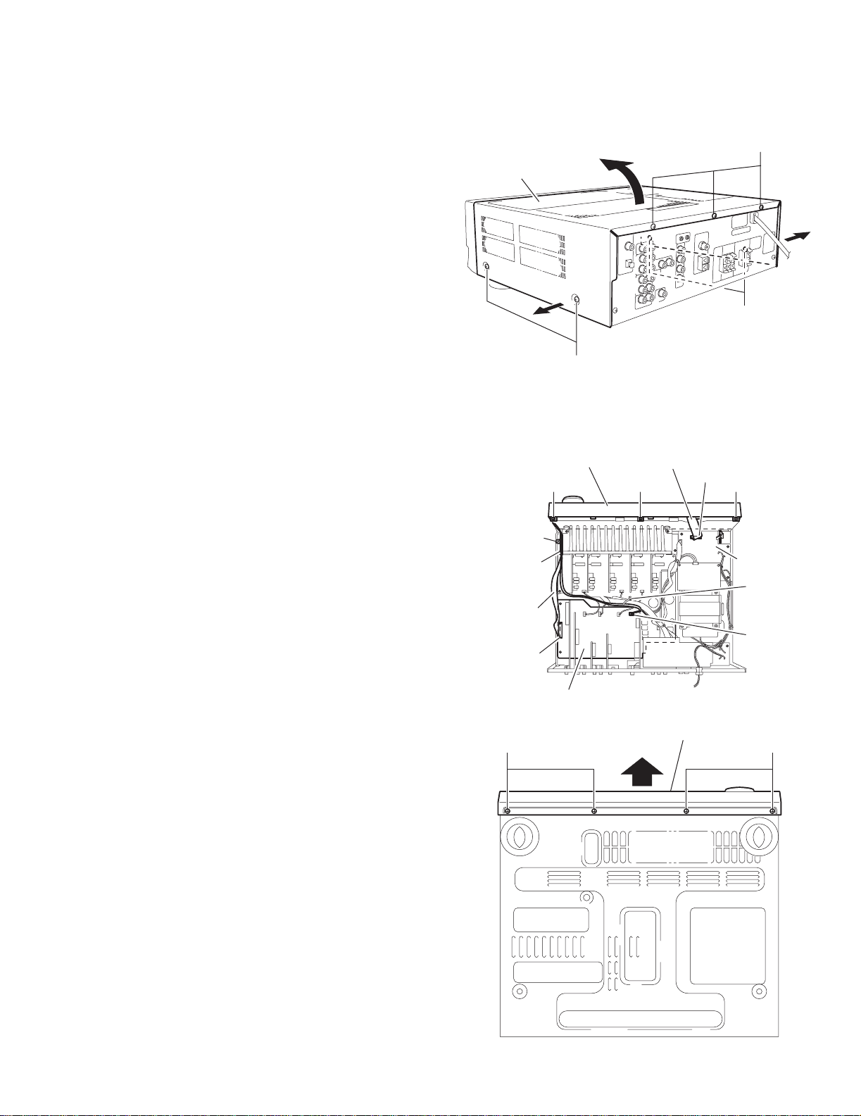
2.3 Removing the rear panel
A
A
(See Fig.4)
• Prior to performing the following procedure, remove the top
cover.
(1) From the back side of the main body, remove the strain re-
lief from the rear panel in the direction of the arrow.
(2) Remove the seventeen screws E and four screws F attach-
ing the rear panel.
E
F
E
Strain relief
F
Rear panel
2.4 Removing the DSP board, audio input board, DVD board and video board
(See Fig.5)
• Prior to performing the following procedure, remove the top
cover and rear panel.
(1) From the top side of the main body, disconnect the DSP
board from the connector CN481 on the audio board.
(2) Disconnect the audio input board from the connector
CN421 on the audio board.
(3) Disco nnect the DVD board from the connector CN431 on
the audio board.
(4) Disco nnect the video bo ard from the connector CN44 1 on
the audio board.
DVD board
CN481
DSP board
udio input board
CN421
Fig.4
Video board
CN441
CN431
Fig.5
EFF
Audio board
2.5 Removing the tuner board
(See Fig.6)
• Prior to performing the following procedure, remove the top
cover and rear panel.
(1) Disconnect the tuner board from the connectors CN411
and CN412 on the audio board.
1-4 (No.22038)
CN412
CN411
Tuner board
udio board
Fig.6
Page 5
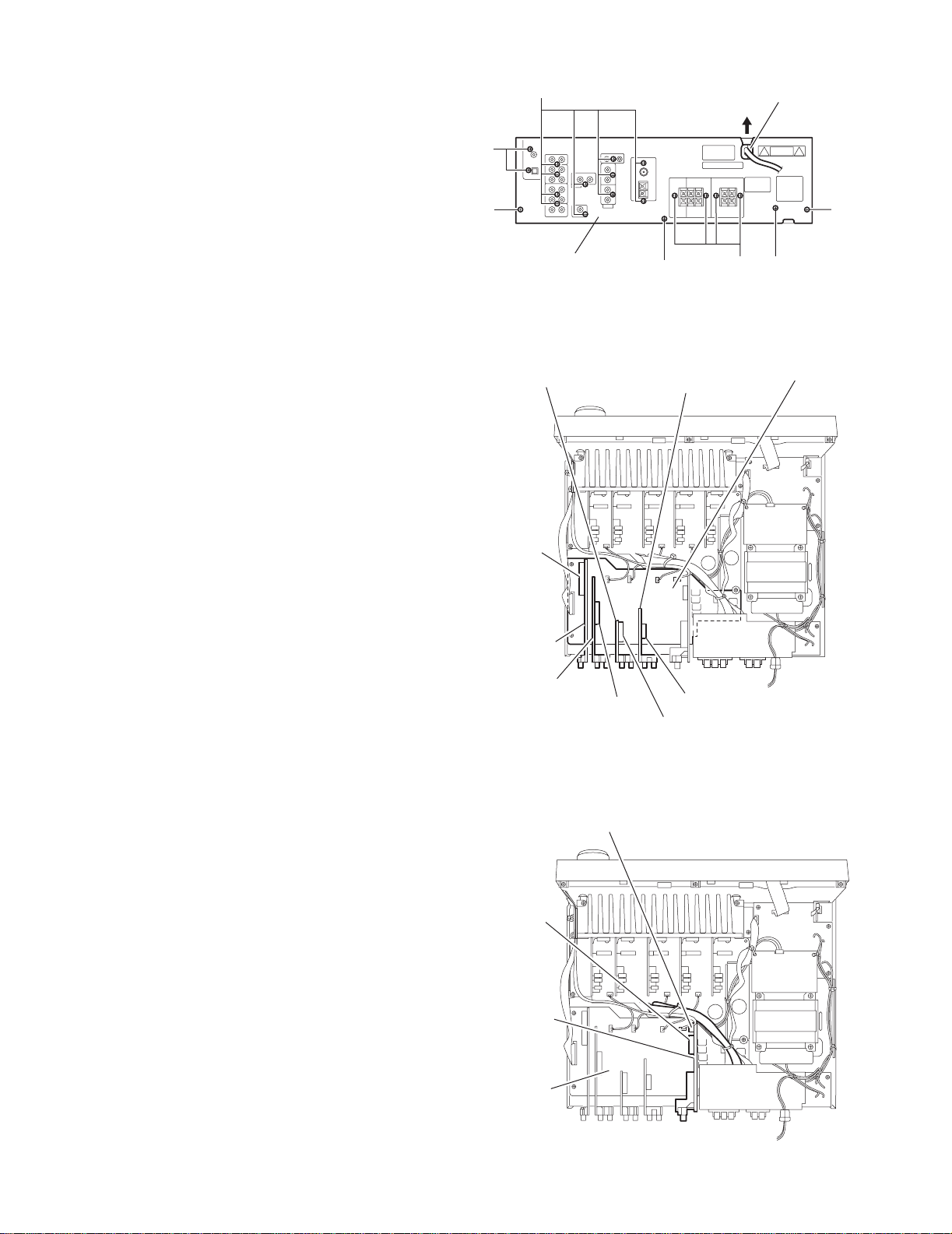
2.6 Removing the audio boar d
(See Fig.7)
• Prior to performing the following procedure, re move the top
cover, rear panel, DSP board, audio input board, DVD board,
video board and tuner board.
(1) From the top side of the main body, disconnect the card
wire from the connector CN402 on the audio board.
(2) Disconnect the parallel wire from the connector CN403.
(3) Disconn ect the relay board from the connector CN4 91 on
the power supply board and audio board.
(4) Disconn ect the wires from the con nectors CN471, CN472
and CN473 on the audio board.
(5) Remove the three screws G attaching the audio board.
(6) Loosen the screw H attaching the audio board.
CN471
CN473
rd wire
G
CN472
Relay board
CN403
2.7 Removing the speaker terminal board
(See Fig.8)
• Prior to performing the following procedure, re move the top
cover and rear panel.
(1) From th e top side of the main body, remove the solders
from the soldered sections a on the speaker terminal
board.
CN402
Audio board
Fig.7
Parallel wires
CN491
G
Soldered sections a
Fig.8
Speaker terminal board
(No.22038)1-5
Page 6
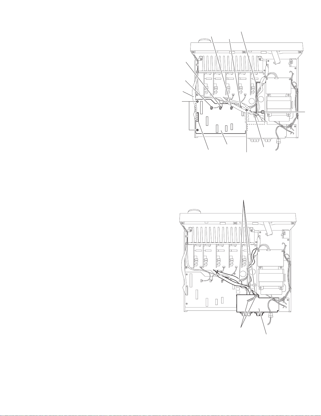
2.8 Removing the main board
r
(See Fig.9)
• Prior to performing the following procedure, remove the top cover.
(1) From the top side of the main body, remove the tie bands fixing the wires.
(2) Remo v e the tie band and wire protection board fixing the card wire.
(3) Remov e the solders from the soldered section b on the speaker terminal board attaching the parallel wires.
(4) Di sco nnect the relay board from the connectors (CN291, CN491) on the power supply board and audio board.
(5) Disco nnect the parallel wire from the connector CN241 on the power supply board.
(6) Disco nnect the wire from the connector CN251 on the power transformer board 1.
(7) Disconnect the wires from the connectors CN471, CN472 and CN473 on the audio board.
(8) Remove the screw H, two screws J and four screws K attaching the main board.
(9) Take out the main board.
Relay board
Power supply board
CN241
Tie band
CN251
Tie band
Wire protection
board
K
Main board
Tie bands
K
K
J
Card wire
CN473
Audio board
CN471
CN472
CN491
Soldered section b
Fig.9
CN291
Power transforme
board 1
H
Parallel wires
Speaker terminal board
1-6 (No.22038)
Page 7
2.9 Removing the heat sink
(See Figs.10 and 11)
• Prior to performing the following procedure, re move the top
cover and main board.
(1) Remove the ten screws L attaching the heat sink. (See
Fig.10)
(2) From the reverse side of the main board, re move the two
screws M attaching the heat sink. (See Fig.11)
2.10Removing the center amp. board, front amp. boards (L /
R) and rear amp. boards (L/R)
(See Figs.10 and 12)
• Prior to performing the following procedure, re move the top
cover and main board.
(1) Remove the ten screws L attaching the heat sink. (See
Fig.10)
(2) Remove the four screws N attachin g the heat sink. (See
Fig.12)
(3) Disconnect the center amp. board from the connector
CN321 on the main board. (See Fig.12)
(4) Disconnect the front amp. board (L) from the connector
CN311 on the main board. (See Fig.12)
(5) Disconn ect the front amp. board (R) from the connector
CN312 on the main board. (See Fig.12)
(6) Disconnect the rear amp. board (L) from the connector
CN331 on the main board. (See Fig.12)
(7) Disconnect the rear amp. board (R) from the connector
CN332 on the main board. (See Fig.12)
Heat sink
Main board
M
L
L
Fig.10
Heat sink
M
Rear amp. board (L)
Rear amp. board (R)
Heat sink
N
CN332 CN331 CN312 CN311 CN321
Main board
Fig.11
Front amp. board (R)
Front amp. board (L)
Center amp. board
N
Main board
Fig.12
(No.22038)1-7
Page 8
2.11Removing the power transformer
r
(See Fig.13)
• Prior to performing the following procedure, remove the top
cover.
(1) From the top side of the main b ody, remove the tie bands
fixing the wires.
(2) Remove the solders from the soldered section c on the
power transformer board 1.
(3) Remove the solders from the soldered sections d on the
power transformer board 2.
(4) Disconnect the wire from the connector CN251 on the pow-
er transformer board 1.
(5) Remov e the four screws P attaching th e power transform-
er.
2.12Removing the power/fuse board
(See Fig.13)
• Prior to performing the following procedure, remove the top
cover.
(1) From the back and top sides of the main body, remove the
screw Q and screw R attaching the power/fuse board.
(2) Remove the solders from the soldered sections e attaching
the power cord.
(3) From the reverse side of the power/fuse board, remove the
solders from the soldered sections f attaching the wires.
2.13Removing the power supply board
(See Fig.14)
• Prior to performing the following procedure, remove the top
cover.
(1) From the top side of the main body, disconnect the parallel
wires from the connectors CN203 and CN241 on the power
supply board.
(2) Disconnect the card wire from the connector CN201 on the
power supply board.
(3) Disco nnect the relay board from the connector CN291 on
the power supply board.
(4) Disco nnect the paral lel wire from the connecto r CN10 1 on
the headphone jack board and remove the tie band.
(5) Remove the solders from the soldered section c on the
power transformer board 1.
(6) Remove the three screws S attaching the power supply
board.
(7) Remo ve the power supply board from the hook g of the
chassis base bracket in the direction of the arrow, take out
the power supply board.
(8) Turn over the power supply board, remove the solders from
the soldered sections h attaching the wires.
2.14Removing the headphone jack board
(See Figs.14 and 15)
• Prior to performing the following procedure, remove the top
cover and front panel assembly.
(1) From the top side of the main body, disconnect the parallel
wire from the connector CN101 on the headphone jack
board. (See Fig.14)
(2) From th e front side of the main body, remove the nut and
screw T attaching the Bracket(phones) to the chassis base.
(See Fig.15)
Power transformer board 1
Tie band
P
P
Soldered sections d
Power cord
CN241
Parallel wires
CN203
CN291
Relay board
Hook g of the
chassis base bracket
Nut
S
T
CN251
Soldered section c
Tie band
P
Power transformer
P
Power transforme
board 2
R
Soldered sections f
Power / Fuse board
Soldered sections e
Q
Fig.13
Card wire
Fig.14
Headphone jack board
Power supply board
CN201
Power transformer board 1
Parallel wire
CN101
Headphone jack
board
Soldered section h
Soldered section c
Bracket(phones)
S
S
1-8 (No.22038)
Chassis base
Fig.15
Page 9
2.15Removing the system control board and power switch board
(See Figs.16 and 17)
• Prior to performing the following procedure, re move the top
cover and front panel assembly.
(1) Pull out the volume and jog knobs from the front side of the
front panel assembly, remove the nut attaching the system
control board. (See Fig.16)
(2) From the back side of the front panel assembly, remove the
nine screws U attaching the system control board. (See
Fig.17)
Reference:
Remove the solders of the soldered section I as required.
(3) Remove the solders of the soldered section i on the system
control board and disconnect the parallel wire. (See Fig.17)
(4) Remove the two screws V attaching the power switch
board. (See Fig.17)
Front panel assembly
U
System control board
Nut
Volume knob
Jog knob
Fig.16
Front panel assembly
Parallel wire
U
Soldered section i
Fig.17
V
U
Power switch board
(No.22038)1-9
Page 10

SECTION 3
Adjustment
3.1 Adjustment method
Tuner section
1. Tuner range
FM 87.5MHz to 108.0MHz
AM 522kHz to 1629kHz
Power amplifier section
Adjustment of idling current
Measurement location TP301 (Lch) , TP302 (Rch)
Adjustment part VR301 (Lch) , VR302 (Rch)
Attention
This adjustment does not obtain a correct adjustment value immediately after the amplifier is
used (state that an internal temperature has risen).
Please adjust immediately after using the amplifier after turning off the power supply of the
amplifier and falling an internal temperature.
<Adjustment method>
1. Set the volume control to minimum during this adjustment. (No signal & No load)
2. Set the surround mode OFF.
3. Turn VR301 and VR302 fully counterclockwise to warm up before adjustment.
If the heat sink is already warm from previous use the correct adjustment can not be made.
4. For L-ch, connect a DC voltmeter between TP301's B216 and B217 (Lch)
and, connect it between TP302's B218 and B219 (Rch).
5. Adjust the VR301 (Lch) and VR302 (Rch) so that the DC voltmeter indicates 2.0mV
immediately after turning the power on.
* It is not abnormal though the idling current might not become 0mA even if it is finished to turn variable
resistance (VR301, VR302) in the direction of counterclockwise.
VR301 (Lch)
Front amp. board (L)
TP301
VR301
CN301
TP301 (Lch)
VR302 (Rch)
Front amp. board (R)
TP302
VR302
CN302
TP302 (Rch)
1-10 (No.22038)
Page 11

SECTION 4
8
Description of major ICs
4.1 LP61L1024S-12-X (IC641) : SRAM
• Pin layout • Block diagram
DD
NC
A16
A14
A12
I/O1
I/O2
I/O3
Vss
1
2
3
4
5
A7
6
A6
7
A5
8
A4
9
A3
10
A2
11
A1
12
A0
13
14
15
16
32
31
30
29
28
27
26
25
24
23
22
21
20
19
18
17
V
A15
CS2
WE
A13
A8
A9
A11
OE
A10
CS1
I/O8
I/O7
I/O6
I/O5
I/O4
DD
• Pin function
I/O1 - I/O8 Data Input/Output
CS1
V
Vss
A0
A16
CS2
CS1
OE
WE
SYMBOL DESCRIPTION
A0 - A16 Address Input
, CS2 Chip Select Inputs
WE
OE
VDD Power Supply
Vss Ground
NC No Connection
DECODER
CONTROL
Write Enable Input
Output Enable Input
CORE
ARRAY
DATA I/O
I/O1
I/O
(No.22038)1-11
Page 12

4.2 AK4527BVQP (IC601): A/D, D/A converter
• Pin layout
4443424140393837363534
1
2
3
4
5
6
7
8
9
10
11
1213141516171819202122
Top View
• Pin function
No. Symbol I/O Function
1 SDOS I SDTO Source Select Pin (Note 1)
"L" : Internal ADC output "H" : DAUX input
2 OSKS I Control Mode Select Pin
"L" : 3-wire Serial "H" : I2C Bus
3 MIS - Soft Mute Pin (Note 1) Connect to GND
When this pin goes to "H" soft mute cycle is initialized.
When returning to "L" the output mute releases.
4 BICK I Audio Serial Data Clock Pin
5 LRCK I/O Input Channel Clock Pin
6 SDTI1 I DAC1 Audio Serial Data Input Pin
7 SDTI2 I DAC2 Audio Serial Data Input Pin
8 SDTI3 I DAC3 Audio Serial Data Input Pin
9 SDTO O Audio Serial Data Output Pin
10 D,AUX - Sub Audio Serial Data Input Pin Connect to GND
11 DFS - Double Speed Sampling Mode Pin (Note 1)
"L" : Normal Speed "H" : Double Speed
12 DEMI - Connect to GND
No internal bonding.
13 DEMO - Zero Input Detect Enable Pin Connect to GND
"L" : mode 7 (disable) at parallel mode
- zero detect mode is selectable by DZFM2-0 bits at serial mode.
- H : mode 0 (DZF is AND of all six channels)
14 MCKO - Output Buffer Power supply Pin 2.7V~5.5V
15 DVDD I Digital Power Supply Pin 4.5V~5.5V
16 DVSS - De-emphasis Pin 0V
17 PD
I Power-Down & Reset Pin
When "L" the AK4527B is powered-down and the control registers are reset to default state.
If the state of P/S or CAD0-1 changes then the AK4527B must be reset by PDN.
18 XTS - Test Pin Connect to GND
This pin should be connected to DVSS.
19 ICKS - Connect to GND No internal bonding.
20 ADIF - Analog Input Format Select Pin Digital Power Supply
H : Full-differential input "L" : Single-ended input
21 CAD1 - Chip Address 1 Pin Connect to GND
33
32
31
30
29
28
27
26
25
24
23
1-12 (No.22038)
Page 13

No. Symbol I/O Function
22 CAD0 O Chip Address 0 Pin Connect to GND
23 LOUT3 O DAC3 Lch Analog Output Pin
24 ROUT3 O DAC3 Rch Analog Output Pin
25 LOUT2 O DAC2 Lch Analog Output Pin
26 ROUT2 O DAC2 Rch Analog Output Pin
27 LOUT1 O DAC1 Lch Analog Output Pin
28 ROUT1 O DAC1 Rch Analog Output Pin
29 LIN- I Lch Analog Negative Input Pin
30 LIN+ I Lch Analog Positive Input Pin
31 RIN- I Rch Analog Negative Input Pin
32 RIN+ I Rch Analog Positive Input Pin
33 VREFL - Zero Input Detect 2 Pin (Note 2) Non Connect
When the input data of the group 1 follow total 8192LRCK cycles with "0" input data this pin
goes to "H".
OVF O Analog Input Overflow Detect Pin (Note 3)
This pin goes to "H" if the analog input of Lch or Rch is overflows.
34 VCOM O Common Voltage Output PinAVDD/2
Large external capacitor around 2.2uF is used to reduce power-supply noise.
35 VREFH - Positive Voltage Reference Input PinAVDD
36 AVDD - Analog Power Supply Pin4.5V~5.5V
37 AVSS - Analog Ground Pin0V
38 XTI - Zero Input Detect 1 Pin (Note 2) Non connect
When the input data of the group 1 follow total 8192 LRCK cycles with "0" input data this pin
goes to "H".
39 XTO I Master Clock Input Pin
40 P1S - Parallel / Serial Select Pin
"L" : Serial control mode "H" : Parallel control mode
41 CS
CSN I Chip select pin in 3-wire serial control mode
42 DIF1 I Audio Data Interface Format 1 Pin in parallel mode
SCL/CCLK I Control Data Clock Pin in serial control mode
43 LOOP0 I Loopback Mode 0 Pin in parallel control mode
SAD/CDTI I/O Control Data Input Pin in serial control mode
44 CDTD I Loopback Mode 1 Pin (Note 1)
Note:
(1) SDOS, SMUTE, DF S, and LOOP1 pins are ORed with register data if P/S = "L".
(2) The group 1 and 2 can be selected by DZFM2-0 bit if P/S = "L" and DZFME = "L".
(3) Thi s pin become s OVF pin if OVFE bit is set to "1" at serial control mode.
(4) All input pins should not be left floating.
I Audio Data Interface Format 0 Pin in parallel mode
This pin should be connected to DVDD at I2C bus control mode
I2C = "L" : CCLK(3-wire Serial) I2C = "H" : SCL(I2CBus)
Enables digital loop-back from ADC to 3 DACs.
I2C = "L" : CDTI(3-wire Serial) I2C = "H" : SDA(I2CBus)
Enable all 3 DAC channels to be input from SDTII.
(No.22038)1-13
Page 14

4.3 BA15218F-XE (IC427,IC609,IC610,IC650,IC651,IC661,IC690,IC691) : Dual operation amplifier
• Pin layout
OUT1 1
-IN1 2
+IN1 3
VEE 4
• Block diagram
Vcc
-IN
+IN
1
2
R1
Q5
Q1
Q2
D1
Q3 Q4
8 Vcc
7 OUT2
6 -IN2
5 +IN2
C2
R5
Q6
Q9
Q8
Q10
Q7
R7
Q11
R6
Q12
R8
Q18Q13
OTHER
CH
Q19
Q17Q16
C1
VEE
4.4 BA15218N (IC403) : Dual Ope. Amp.
• Pin layout / Block diaglam
+
1
-
1 2 3 4 5 6 7 8
OUT1 +IN1 +IN1
GND
+
-
+IN2 -IN2 OUT2
R3R2
R4
Q14 Q15Q114
R9
OUTPUT
2
Vcc
1-14 (No.22038)
Page 15

4.5 GP1UM281X (IC703) : Dual operation amplifier
GND Vcc Vout
R
L
Amp
4.6 IC-PST9139-T(IC403) : Regulator
• Terminal layout
123
B.P.FLimiter
Demodulator
Integrator
Comparator
• Block diagram
4.7 IMX9-W (IC652, IC662, IC682): Driver
• Pin layout & Block diagram
C
1
B
2
E
3
6
5
4
CO1
E
B
C
VCC
2
OUT
1
OP1
GND
3
(No.22038)1-15
Page 16

4.8 LA1838 (IC102) : FM AM IF AMP&detector, FM MPX Decoder
• Block Diagram
30
ALC
BUFF
FM
S-METER
FM IF
1
29
AM
OSC
S-CLRVE
PM
DET
2
28
REG
AM
MIX
SD
COMP
AM/FM
IF-BUFF
3
27
FM
RF.AMP
AM IF
4
26
AGC
AM
S-METER
GND
25
24
DET
TUNING
DRIVE
5
6
STEREO
DRIVE
7
22
23
P-DET
VCC
89
VCO
384KHz
21
DECODER
ANIT-BIRDIE
10
20
STEREO
5N
SW
FF
38k
11
18
19
MUTE
FF
/
19k
2
12 13
FF
19k
17 16
/LS
14
PILOT
DET
15
• Pin Function
Pin No. Symbol I/O Function
1 FM IN I This is an input terminal of FM IF signal.
2 AM MIX O This is an out put terminal for AM mixer.
3 FM IF I Bypass of FM IF
4 AM IF I Input of AM IF Signal.
5 GND - This is the device ground terminal.
6
7
TUNED
STEREO
O When the set is tunning,this terminal becomes "L".
O Stereo indicator output. Stereo "L", Mono: "H"
8 VCC - This is the power supply terminal.
9 FM DET - FM detect transformer.
10 AM SD - This is a terminal of AM ceramic filter.
11 FM VSM O Adjust FM SD sensitivity.
12 AM VSM O Adjust AM SD sensitivity.
13 MUTE I/O When the signal of IF REQ of IC121(LC72131) appear, the signal of FM/AM IF output. //Muting
control input.
14
15
FM/AM
MONO
/ST
I Change over the FM/AM input. "H" :FM, "L" : AM
O Stereo : "H", Mono: "L"
16 L OUT O Left channel signal output.
17 R OUT O Right channel signal output.
18 L IN I Input terminal of the Left channel post AMP.
19 R IN I Input terminal of the Right channel post AMP.
20 RO O Mpx Right channel signal output.
21 LO O Mpx Left channel signal output.
22 MPX IN I Mpx input terminal
23 FM OUT O FM detection output.
24 AM DET O AM detection output.
25 AM AGC I This is an AGC voltage input terminal for AM
26 AFC - This is an output terminal of voltage for FM-AFC.
27 AM RF I AM RF signal input.
28 REG O Register value between pin 26 and pin28 besides the frequency width of the input signal.
29 AM OSC - This is a terminal of AM Local oscillation circuit.
30 OSC BUFFER O AM Local oscillation Signal output.
1-16 (No.22038)
Page 17

4.9 LC72136N (IC121) : PLL frequency synthesizer
•Pin layout
1
XT
FM/AM
CE
DI
CLOCK
DO
FM/ST/VCO
AM/FM
SDIN
2
3
4
5
6
7
8
9
10
11
22
21
20
19
18
17
16
15
14
13
12
XT
GND
LPFOUT
LPFIN
PD
VCC
FMIN
AMIN
IFCONT
IFIN
• Block diagram
1
22
16
15
3
4
5
6
17
21
1/2
C
I/F
2B
Power
on
Reset
Data Shift Register & Latch
7821113
• Pin function
Pin
Symbol I/O Function
No.
1 XT I X'tal oscillator connect (75kHz)
2FM
/AM O LOW:FM mode
3 CE I When data output/input for 4pin(input)
and 6pin(output): H
4 DI I Input for receive the serial d ata from
controller
5 CLOCK I Sync signal input use
6 DO O Data output for Controller Output port
7 FM/ST/VCO O Low: MW mode
8AM
/FM O Open state after the power on reset
9 LW I/O Input/output port
10 MW I/O Input/output port
11 SDIN I/O Data input/output
12 IFIN I IF counter signal input
Reference
Driver
Swallow Counter
Swallow Counter
1/16,1/17 4bit
1/16,1/17 4bit
12bit
Programmable
DriverS
Phase
Detector
Charge Pump
Unlock
Detector
Universal
Counter
Pin
Symbol I/O Function
No.
18
19
20
12
13 IFCONT O IF signal output
14 - Not use
15 AMIN I AM Local OSC signal output
16 FMIN I FM Local OSC signal input
17 VCC - Power suplly(VDD=4.5-5.5V)
When power ON:Reset circuit move
18 PD O PLL charge pump output (H: Local
OSC frequency Height than Reference frequency.L: Low Agreement:
Height impedance)
19 LPFIN I Input for active lowpassfilter of PLL
20 LPFOUT O Output for active lowpassfilter of PLL
21 GND - Connected to GND
22 XT
I X'tal oscillator(75KHz)
(No.22038)1-17
Page 18

4.10 M62446AFP-X (IC428): 6 channel electronic volume
• Pin layout & Block diagram
OUT4
OUT3
OUT2
OUT1
AVD D
SWin
GNDS
SRin
SLin
GNDC
Cin
GNDR
Rin
GNDL
Lin
BYPASSR
BYPASSL
LTR E
LBASS3
LBASS2
LBASS1
10
11
12
13
14
15
16
17
18
19
20
21
1
2
3
4
5
6
7
8
9
OUTPUT
PORT
tone
volume
volume
volume
volume
volume
volume
MCU
I/F
tone
42
41
40
39
38
37
36
35
34
33
32
31
30
29
28
27
26
25
24
23
22
DVDD
CLK
DATA
LATCH
DGND
AGND
SWout
SRout
SLout
Cout
Rout
Lout
AVS S
CL1
CL2
CR1
CR2
RTRE
RBASS3
RBASS2
RBASS1
1-18 (No.22038)
Page 19

• Pin function
Pin No. Symbol I/O Function
1 OUT4 O PORT output 4
2 OUT3 O PORT output 3
3 OUT2 O PORT output 2
4 OUT1 O PORT output 1
5 AVDD - Analog positive power supply terminal
6 SWin I Volume input
7 GNDS - Ground terminal
8 SRin I Volume input
9 SLin I Volume inp ut
10 GNDC - Ground termin al
11 Cin I Volume input
12 GNDR - Ground termin al
13 Rin I Tone input
14 GNDL - Ground terminal
15 Lin I Tone input
16 BYPASSR I R channel volume input
17 BYPASSL I L channel volume input
18 LTRE I Tone treble frequency adjusting terminal
19 LBASS3 I Tone bass frequency adjusting terminal
20 LBASS2 I Tone bass frequency adjusting terminal
21 LBASS1 I Tone bass frequency adjusting terminal
22 RBASS1 I Tone bass frequency adjusting terminal
23 RBASS2 I Tone bass frequency adjusting terminal
24 RBASS3 I Tone bass frequency adjusting terminal
25 RTRE I Tone treble frequency adjusting terminal
26 CR2 O Tone output terminal
27 CR1 I R channel volume input
28 CL2 O Tone output terminal
29 CL1 I L channel volume input
30 AVSS - Analog negative power supply terminal
31 Lout O L channel output
32 Rout O R channel output
33 Cout O Volume output
34 SLout O Volume output
35 SRout O Volume output
36 SWout O Volume output
37 AGND - Analog ground termi n al
38 DGND - Digital ground terminal
39 LATCH I Latch input terminal
40 DATA I Data input terminal
41 CLK I Data transfer clock input terminal
42 DVDD - Digital power supply terminal
(No.22038)1-19
Page 20

4.11 MM1563DF-X (IC681) : Regulator
• Pin layout
756
(TOP VIEW)
1
234
• Block diagram
V
IN
7
Bias
Cont
5
Thermal
shutdown
GND
3
• Pin function
Pin No. Symbol Function
1 Vo Output pin
2 NC Not connect
3 GND Ground
4 Cn Noise decrease pin
5 CON T Control pin
Driver
Current
limiter
4
Cn
Reference
Vo
1
CONT
H
L
Output
ON
OFF
6 Sub Substrate pin, The 6pin must be connected to GND.
7 VIN Input pin
1-20 (No.22038)
Page 21

4.12 MM1613DN-X (IC683) : Regulator
• Pin layout • Block diagram
Vin
5
54
(TOP VIEW)
1
23
Cont
GND
1
2
Bias
Reference
3
Cn
Driver
Thermal
shutdown
• Pin function
Pin No. Symbol Function
1 Cont ON/OFF Control pin
Cont
H
L
Vo
ON
OFF
Cont pin must be connected with VIN pin, if it is not used.
2 GND Ground
3 Cn Noise decrease pin, Connecting 0.01uF capacitor can decrease output noise.
4 Vout If the noise decrease capacitor is not connected, the pin may be influenced by outside noise.
Output pin, The capacitor must be connected with output pin more than 1uF.
5 V in In put pin
The capacitor is required to connect with input pin more than 1uF.
Current
limiter
Vout
4
4.13 MM74HC08SJ-X (IC611) : Quad. 2-input AND gates
• Pin layout & Block diagram
Vcc
A1
B1
Y1
A2
B2
Y2
GND
1
2
3
4
5
6
7
14
13
12
11
10
9
8
B4
A4
Y4
B3
A3
Y3
(No.22038)1-21
Page 22

4.14 MM74HCU04SJ-X (IC621) : Inverter
• Pin Layout
11A
21Y
32A
14
13
12
VCC
6A
6Y
4.15 NC7ST32P5-X (IC672) : 2-Input OR Gate
• Pin layout & Block diagram • Truth table
Vcc Y
54
INPUTS OUTPUT
ABY
LLL
LHH
1
23
A B GND
HLH
HHH
H : HIGH logic level
L : LOW logic level
4.16 NJM2246D (IC501) : Video switch
• Pin layout & Block diaglam
GND
8
6dB
AMP.
Vout
7
V+
6
Vin3
5
Control input - output signal
CTL 1 CTL 2 Output
LLVIN 1
HLVIN 2
L/H H VIN 3
42Y
53A
63Y
7
11
10
9
8GND
5A
5Y
4A
4Y
1
Vin1
1-22 (No.22038)
2
CTL1
3
Vin2
BIAS
4
CTL2
Page 23

4.17 MN101C35DME (IC701) : System control & FL driver
•Pin layout
100 76
1
75
25
51
26 50
• Pin function
Pin No. Symbol I/O Function
1 TXD / SBO0 / P00 I VOL. JOG IN_1
2 RXD / SBI0 / P01 I VOL. JOG IN_2
3 SBT0 / P02 I/O DATA (PLL)
4 SBO1 / P03 O CLK (PLL)
5 SBI1 / P04 O CE (PLL)
6 SBT1 / P05 I VIDEO S/C DVD
7 BUZZER / P06 I VIDEO S/C VCR
8VDD-+5V
9 OSC2 O 8MHz oscillation te rmi na l
10 OSC1 I 8MHz oscillation terminal
11 VSS - Ground
12 XI I Connect to ground
13 XO O Not connect
14 MMOD I Connect to ground
15 VREF- - Ground
16 AN0 / PA0 I Key input 1 (7 key)
17 AN1 / PA1 I Key input 2 (7 key)
18 AN2 / PA2 I Key input 3 (7 key)
19 AN3 / PA3 I Key input 4 (7 key)
20 AN4 / PA4 I Key input 5 (7 key)
21 AN5 / PA5 I INH IN
22 AN6 / PA6 I Chip select 1
23 AN7 / PA7 I Chip select 2
24 VREF+ - +5V
25 P07 I VIDEO S/C DBS
26 /RST / P27 I Reset input
27 RMOUT / TM0IO / P10 O RDS CLK OUT (RDS)
28 TM1IO / P11 I DCS input
29 TM2IO / P12 O DCS output
30 TM3IO / P13 I AV link VCR input
31 TM4IO / P14 O AV link VCR output
32 P15 I/O RDS DATA (RDS)
33 IRQ0 / P20 I PROTECTOR IN
34 SENS / IRQ1 / P21 I Remocon input
35 IRQ2 / P22 I TUNED IN (TUNER)
36 IRQ3 / P23 I STEREO IN (TUNER)
37 IRQ4 / P24 I RDS DAVN (RDS)
38 P25 I Self check input
39 SBO2 / P30 O COMMAND (DSP)
40 SBI2 / P31 I STATUS (DSP)
41 SBT2 / P32 O CLK (DSP)
42 P50 I MULTI. JOG_1
43 P51 I MULTI. JOG_2
44 P52 O RELAY S
45 P53 O RELAY C
46 P54 O RELAY L/R 1
47 DGT17 / P67 O RELAY L/R 2
48 DGT16 / P66 O RELAY HEADPHONE
49 DGT15 / P65 O GRID 16
50 DGT14 / P64 O GRID 15
Pin No. Symbol I/O Function
51 DGT13 / P63 O GRID14
52 DGT12 / P62 O GRID13
53 DGT11 / P61 O GRID12
54 DGT10 / P60 O GRID11
55 DGT9 / P41 O GRID10
56 DGT8 / P40 O GRID9
57 SEG0 / DGT7 / P77 O GRID8
58 SEG1 / DGT6 / P76 O GRID7
59 SEG2 / DGT5 / P75 O GRID6
60 SEG3 / DGT4 / P74 O GRID5
61 SEG4 / DGT3 / P73 O GRID4
62 SEG5 / DGT2 / P72 O GRID3
63 SEG6 / DGT1 / P71 O GRID2
64 SEG7 / DGT0 / P70 O GRID1
65 SEG8 / P87 O SEGMENT1
66 SEG9 / P86 O SEGMENT2
67 SEG10 / P85 O SEGMENT3
68 SEG11 / P84 O SEGMENT4
69 SEG12 / P83 O SEGMENT5
70 SEG13 / P82 O SEGMENT6
71 SEG14 / P81 O SEGMENT7
72 SEG15 / P80 O SEGMENT8
73 SEG16 / P97 O SEGMENT9
74 SEG17 / P96 O SEGMENT10
75 SEG18 / P95 O SEGMENT11
76 SEG19 / P94 O SEGMENT12
77 SEG20 / P93 O SEGMENT13
78 SEG21 / P92 O SEGMENT14
79 SEG22 / P91 O SEGMENT15
80 SEG23 / P90 O SEGMENT16
81 SEG24 / PC2 O
82 SEG25 / PC1 O
83 SEG26 / PC0 O
84 SEG27 / PB7 O
85 SEG28 / PB6 O
86 SEG29 / PB5 O RESET (DSP)
87 SEG30 / PB4 O READY (DSP)
88 SEG31 / PB3 O POWER ON
89 SEG32 / PB2 O SOURCE MUTE
90 SEG33 / PB1 O SUBWOOFER MUTE
91 SEG34 / PB0 O TUNER MUTE
92 SEG35 / PD7 O STANDBY LED
93 SEG36 / PD6 O SURROUND
94 SEG37 / PD5 O DATA (A.SW)
95 SEG38 / PD4 O CLK (A.SW)
96 SEG39 / PD3 O STB (A.SW)
97 SEG40 / PD2 O LATCH (VOL)
98 SEG41 / PD1 O DATA (VOL)
99 SEG42 / PD0 O CLK (VOL)
100 VPP - VPP
(No.22038)1-23
Page 24

4.18 SAA6588 (IC191) : RDS Detector
• Terminal Layout • Pin Function
Pin
Symbol I/O Function
MRO
NC
GND
OSCO
OSCI
1
2
3
4
5
20
19
18
17
16
NC
CIN
SCOUT
Vref
MPX
No.
1 MRO O Multi-path rectifier output
2 NC - Non connect
3 GND I Test control input pin
4 OSCO O Oscillator output
5 OSCI I Oscillator input
6 VSSD - Digital ground (0V)
VSSD
VDDD
DAVN
SDA
SCL
6
7
8
9
10
15
14
13
12
11
VSSA
VDDA
NC
GND
NC
7 VDDD - Digital power supply (5V)
8 DAVN O Data available output (active LOW)
9 SDA I/O IC-bus serial data I/O
10 SCL I IC-bus serial clock input
11 NC - Non connect
12 GND - Connect to ground
13 NC - Non connect
14 VDDA - Analog power supply (5V)
15 VSSA - Connect to ground
16 MPX I Multiplex input signal
17 Vref O Reference voltag e output
18 SCOUT O Band-pass filter output
19 CIN O Comparator output
20 NC I Level input
• Block Diagram
MPX
AFIN
LVIN
VDDA
16
13
20
14
VSSA
SCOUT
57 kHz
8th ORDER
BAND-PASS
PAUSE
DETECTOR
POWER
SUPPLY
AND RESET
15
18
17
Vref
19
CLOCK
COMPARATOR
MULTI-PATH
DETECTOR
TEST
CONTROL
3
TCON
RDS/RDBS
DEMODULATOR
SIGNAL QUALITY
DETECTOR
OSCILLATOR
AND CLOCK
1
MRO
OSCI OSCO
VDDDCIN
7
DAVN
12
MAD
11
10
8
2
9
PSWN
MPTH
SDA
SCL
RDS/RDBS
DECODER
INTERFACE
REGISTER
IC-BUS SLAVE
TRANSCEIVER
5
4
6
VSSD
1-24 (No.22038)
Page 25

4.19 TC74HC4072AF-X (IC612) : OR gate
• Block diagram
1Y
1
1A
2
1B
3
1C
4
1D
5
NC
6
GND
7
4.20 TC9164AN (IC402) : Analog switch
• Pin layout & Block Diagram
R-S1
S-2
VDD
S-3
27
26
252824
S-4
&
SHIFT
RESISTOR
COM-1
23
LATCH
S-5
22
S-6
21
COM-2
20
14
13
12
11
10
9
8
S-7
19
Vcc
2Y
2D
2C
2B
2A
NC
S-8
18
• Truth table
ABCDY
HXXXH
XHXXH
XXHXH
XXXHH
LLLLL
X : Don't care
COM316DATA15CK
17
VSS
2
L-S1
3
S-2
415
S-3
&
SHIFT
RESISTOR
S-4
LATCH
6
OM-1
7
S-5
8
S-6
9
OM-2
10
S-7
11
S-8
SHIFT RESISTOR
12
13ST14
COM3
GND
(No.22038)1-25
Page 26

4.21 TC9162AF-X (IC423) : Analog switch
• Pin Layout
28272625242322212019181716
123
• Block Diagram
L-S1
L-S2
L-COM1
L-S3
L-S4
L-COM2
15
4
5
6
789
2
3
4
5
6
7
1011121314
VSS
1
GND VDD
14
28
27
26
25
24
23
22
R-S1
R-S2
R-COM1
R-S3
R-S4
R-COM2
L-S5
L-S6
L-COM3
L-S7
L-COM4
ST
8
9
10
11
12
13
LEVEL SHIFTER
LATCH CIRCUIT
SHIFT REGISTER
LATCH CIRCUIT
LEVEL SHIFTER
21
20
19
18
17
16
15
R-S5
R-S6
R-COM3
R-S7
R-COM4
DATA
CK
1-26 (No.22038)
Page 27

4.22 TC9446F-025 (IC631): Digital signal processor for dolby digital (AC-3) / DTS audio decode
• Pin Function
Pin No. Symbol I/O Function
1 RST I Reset signal input terminal (L:reset H: normal operation)
2 MIMD I Microcomputer interface mode selection input terminal (L:serial H:IC bus)
3 MICS I Microcomputer interface chip select input terminal
4 MILP I Microcomputer interface latch pulse input
5 MIDIO I/O Microcomputer interface data I/O terminal
6 MICK I Microcomputer interface clock input terminal
7 MIACK O Microcomputer interface acknowledge output terminal
8~11 FI0~3 I Flag input terminal 0~3
12 IRQ I Interrupt input terminal
13 VSS - Digital ground terminal
14 LRCKA I Audio interface LR clock input terminal A
15 BCKA I Audio interface bit clock input terminal A
16~18 SDO0~2 O Audio interface data output terminal 0
19 SD03 - Non connect
20 LRCKB I Audio interface LR clock input terminal B
21 BCKB I Audio interface bit clock input terminal B
22 SDT0 I Audio interface data input terminal 0
23 SDT1 I Audio interface data input terminal 1
24 VDD - Power supply for digital circuit
25 LRCKOA O Audio interface LR clock output terminal A
26 BCKOA O Audio interface bit clock output terminal A
27, 28 TEST0,1 I Test input terminal 0/1 (L:test H: normal operation)
29~30 LRCKOBBCKOB - Non connect
31 TXO O SPDIF Output
32, 33 TEST2,3 I Test input terminal (L:test H: normal operation)
34 RX I SPDIF input terminal
35 VSS - Ground terminal for digital circuit
36 TSTSUB0 I Test sub input terminal 0 (L:test H: normal operation)
37 FCONT O VCO Frequency control output terminal
38, 39 TSTSUB1TSTSUB2 I Test sub input terminal 12 (L:test H: normal operation)
40 PDO O Phase detect signal output terminal
41 VDDA - Power supply for analog circuit
42 PLON I Clock selection input terminal (L:external clock H:VCO clock)
43 AMPI I amplifier input terminal for LPF
44 AMPO O amplifier output terminal for LPF
45 CKI I External clock input terminal
46 VSSA - Ground terminal for analog circuit
47 CKO O DIR Clock output terminal
48 LOCK O VCO Lock output terminal
49 VSS - Ground terminal for digital circuit
50 WR O External SRAM writing signal output terminal
51 OE O External SRAM output enable signal output terminal
52 CE O External SRAM chip enable signal output terminal
53 VDD - Power supply terminal for digital circuit
54~61 IO7~0 I/O External SRAM data I/O terminal 7~0
62 VSS - Ground terminal for digital circuit
63~70 AD0~7 O External SRAM address output terminal 0~7
71 VDD - Power supply terminal for digital circuit
72~80 AD8~16 O External SRAM address output terminal 8~16
81 VSS - round terminal for digital circuit
82~89 PO0~7 O General purpose output terminal 0~7
90 VDDDL - Power supply terminal for DLL
91 LPFO O LPF output terminal for DLL
92, 93 DLON,DLCKS I Refer to the undermentioned table
94 SCKO - Non connect
95 VSSDL - Ground terminal for DLL
96 SCKI I External system clock input terminal
97 VSSX - Ground terminal for oscillation circuit
98, 99 XO,XI I/O Oscillation I/O terminal
100 VDDX - Power supply terminal for oscillation circuit
DLCKS terminal DLON terminal DLL clock setting
L L SCKI input (DLL circuit OFF)
L H Four times XI clock
H L Three times XI clock
H H Six times XI clock
(No.22038)1-27
Page 28

4.23 UPD784215AGC167 (IC671): Digital signal controller
• Pin layout
~
100 76
1
~
25
~
26 50
• Pin function
Pin No. Symbol I/O Function
1~8 - Non connect
9 VDD - Power supply terminal
10 X2 O Connecting the crystal oscillator for system main clock
11 X1 I Connecting the crystal oscillator for system main clock
12 VSS - Connect to GND
13 XT2 O Connecting the crystal oscillator for system sub clock
14 XT1 I Connecting the crystal oscillator for system sub clock
15 RESET I System reset signal input
16 AUT ODATA I Output of DSP to general-purpose port
17 LOCK I Output of DSP to general-purpose port
18 DIGITAL0 I Output of DSP to general-purpose port
19 FORMAT I Output of DSP to general-purpose port
20 CHANNEL I Ou tput of DSP to general-purpose port
21 ERR I Output of DSP to general-purpose port
22 REST IN I Reset signa l input
23 AVDD - Power supply terminal
24 AVREF0 - Connect to GND
25 - Connect to GND
26 - Connect to GND
27 - Connect to GND
28 - Connect to GND
29 - Connect to GND
30 - Connect to GND
31 - Connect to GND
32 - Connect to GND
33 AVSS - Connect to GND
34,35 - Non connect
36 AV REF1 - Power supply terminal
37 RX - Not use
38 TX - Not use
39 - Non connect
40 DSPCOM I Communication port from IC701
41 DSPSTS O Status communication port to IC701
42 DSPCLK I Clock input from IC701
43 DSPRDY I Ready signal input from IC701
44 - Non connect
75
~
51
1-28 (No.22038)
Page 29

Pin No. Symbol I/O Function
45 MIDIO IN I/O Interface I/O terminal with microcomputer
46 MIDIO OUT I/O Interface I/O terminal with microcomputer
47 MICK O Interface I/O terminal with microcomputer of clock signal
48 MICS O Interface I/O terminal with microcomputer of chip select
49 MILP O Interface I/O terminal with microcomputer
50 MIACK O Interface I/O terminal with microcomputer
51 - Non connect
52 - Non connect
53 DSPRST O Reset signal output of DSP
54~63 - Non connect
64 CODEC OUT I/O Interface I/O terminal with microcomputer
65 CODEC IN I/O Interface I/O terminal with microcomputer
66 CODEC CLK O Interface I/O terminal with microcomputer of clock signal
67 CODEC CS O Interface I/O terminal with microcomputer of chip select
68 CODEC XTS - Non connect
69 - Non connect
70 - Non connect
71 PD O Reset signal output
72 GND - Connect to GND
73 - Non connect
74 - Non connect
75 - Non connect
76 - Non connect
77 - Non connect
78 - Non connect
79 - Non connect
80 - Non connect
81 VDD - Power supply
82 - Non connect
83 - Non connect
84 ANA/T-TONE O Test tone control
85 LEF-MIX O Control at output destination of LFE channel
86 - Non connect
87 D.MUTE O Mute of the digital out terminal is controlled
88 S.MUTE O Mute of the audio signal is controlled
89 O Non connect
90 ASW1 O Selection of digital input selector
91 ASW2 - Selection of digital input selector
92 ASW3 - Selection of digital input selector
93 ASW4 - Selection of digital input selector
94 TEST - Test terminal
95 - Non connect
96 - Non connect
97 - Non connect
98 - Non connect
99 - Non connect
100 - Non connect
(No.22038)1-29
Page 30

VICTOR COMPANY OF JAPAN, LIMITED
AV & MULTIMEDIA COMPANY AUDIO/VIDEO SYSTEMS CATEGORY 10-1,1chome,Ohwatari-machi,Maebashi-city,371-8543,Japan
(No.22038)
Printed in Japan
WPC
 Loading...