

Page 1
SERVICE MANUAL
AUDIO/VIDEO CONTROL RECEIVER
RX-5000VBK
RX-5001VGD
UF
US
RX-5000VBK
RX-5001VGD
Area Suffix
China
Singapore
POWER
TV
CD
VCR
AUDIO
TAPE/MD
SURROUND
TESTDELAY
5
321
EFFECT
FM/AM
– CENTER +
5
54
6
5
VCR
– REAR•L +
5
98
7/P
MENU
SOUND
DVD
CONTROL
– REAR•R +
+10
10
ENT
DVD MULTI
CD-DISC
TV VOL.
+
PHONO
ONE TOUCH
OPERATION
VOLUME
MUTING
SLEEP
8
4
1
RM-SR558U REMOTE CONTROL
–
TV CH–TV/VIDEO
+
+
+
VCR CH
–
–
£
4
1
7
RX-5000V AUDIO/VIDEO CONTROL RECEIVER
STANDBY
POWER
SPEAKERS
PHONES
12
DVD MULTICDDVD
PHONO
OFF_ ON
Contents
Safety precautions ---------------- 1-2
Disassembly method ------------- 1-3
Adjustment method --------------- 1-5
MASTER VOLUME
– +
ADJUSTBASS BOOST
SETTING
VCR
FM
SURROUND MULTI CURSOR
ONE TOUCH OPERATION
AM
TAPE/MD
SOURCE NAME
INPUT ATT.
MEMORY
Description of major ICs --------- 1-6
Internal connections for
FL display tube ----- 1-15
COPYRIGHT 2000 VICTOR COMPANY OF JAPAN, LTD.
No.20883
Nov. 2000
Page 2
RX-5000VBK/RX-5001VGD
Safety Precautions
1. This design of this product contains special hardware and many circuits and components specially
for safety purposes. For continued protection, no changes should be made to the original design
unless authorized in writing by the manufacturer. Replacement parts must be identical to those
used in the original circuits. Services should be performed by qualified personnel only.
2. Alterations of the design or circuitry of the product should not be made. Any design alterations of
the product should not be made. Any design alterations or additions will void the manufacturer`s
warranty and will further relieve the manufacture of responsibility for personal injury or proper ty
damage resulting therefrom.
3. Many electrical and mechanical par ts in the products have special safety-related characteristics.
These characteristics are often not evident from visual inspection nor can the protection afforded
by them necessarily be obtained by using replacement components rated for higher voltage,
wattage, etc. Replacement parts which have these special safety characteristics are identified in
the Parts List of Service Manual. Electrical components having such features are identified by
shading on the schematics and by ( ) on the Parts List in the Service Manual. The use of a
substitute replacement which does not have the same safety characteristics as the recommended
replacement parts shown in the Parts List of Service Manual may create shock, fire, or other
hazards.
4. The leads in the products are routed and dressed with ties, clamps, tubings, barriers and the
like to be separated from live parts, high temperature parts, moving parts and/or sharp edges
for the prevention of electric shock and fire hazard. When service is required, the or iginal lead
routing and dress should be observed, and it should be confirmed that they have been returned
to normal, after re-assembling.
5. Leakage currnet check (Electrical shock hazard testing)
After re-assembling the product, always perform an isolation check on the exposed metal parts
of the product (antenna terminals, knobs, metal cabinet, screw heads, headphone jack, control
shafts, etc.) to be sure the product is safe to operate without danger of electrical shock.
Do not use a line isolation transformer during this check.
Plug the AC line cord directly into the AC outlet. Using a "Leakage Current Tester", measure
the leakage current from each exposed metal parts of the cabinet , particularly any exposed
metal part having a return path to the chassis, to a known good earth ground. Any leakage
current must not exceed 0.5mA AC (r.m.s.)
Alternate check method
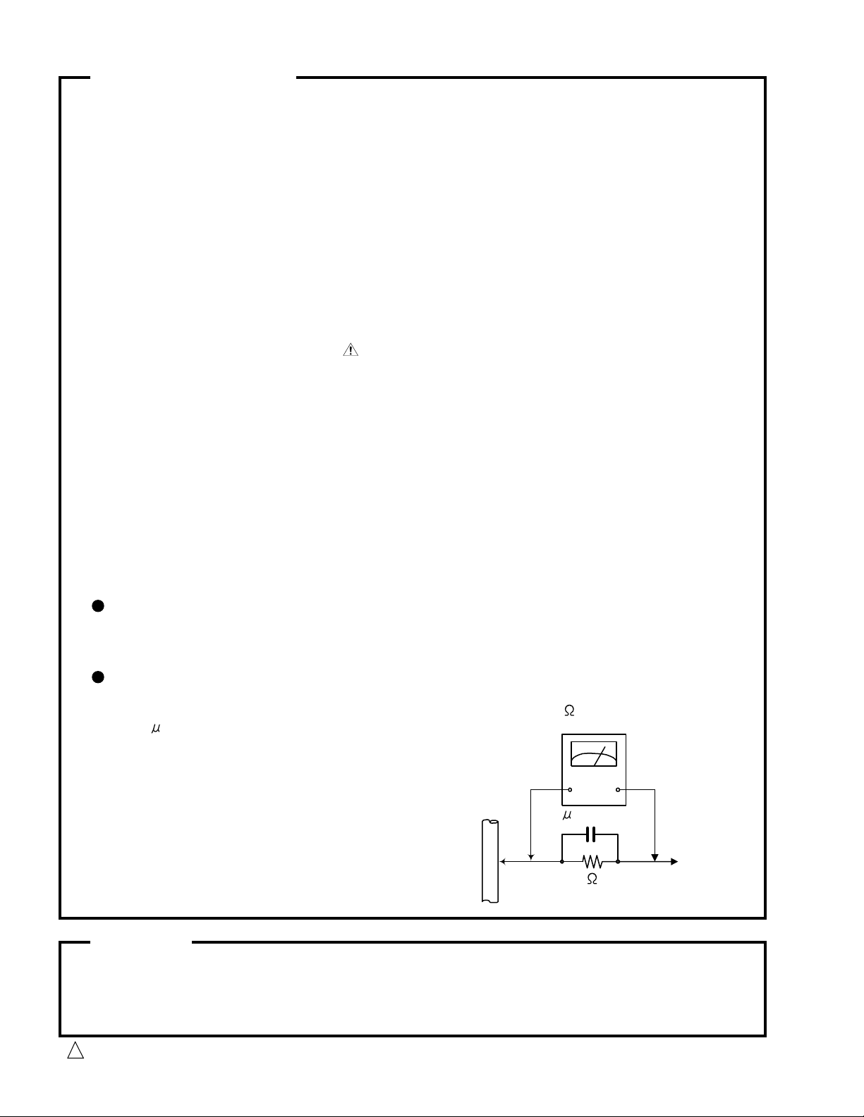
Plug the AC line cord directly into the AC outlet. Use an AC voltmeter having, 1,000 ohms
per volt or more sensitivity in the following manner. Connect a 1,500 10W resistor paralleled by
a 0.15 F AC-type capacitor between an exposed
metal part and a known good earth ground.
Measure the AC voltage across the resistor with the
AC voltmeter.
Move the resistor connection to eachexposed metal
part, par ticularly any exposed metal part having a
return path to the chassis, and meausre the AC
voltage across the resistor. Now, reverse the plug in
the AC outlet and repeat each measurement. voltage
measured Any must not exceed 0.75 V AC (r.m.s.).
This corresponds to 0.5 mA AC (r.m.s.).
0.15 F AC TYPE
1500 10W
Good earth ground
AC VOLTMETER
(Having 1000
ohms/volts,
or more sensitivity)
Place this
probe on
each exposed
metal part.
Warning
1. This equipment has been designed and manufactured to meet international safety standards.
2. It is the legal responsibility of the repairer to ensure that these safety standards are maintained.
3. Repairs must be made in accordance with the relevant safety standards.
4. It is essential that safety critical components are replaced by approved parts.
5. If mains voltage selector is provided, check setting for local voltage.
Burrs formed during molding may be left over on some parts of the chassis. Therefore,
pay attention to such burrs in the case of preforming repair of this system.
1-2
CAUTION
!
Page 3
RX-5000VBK/RX-5001VGD
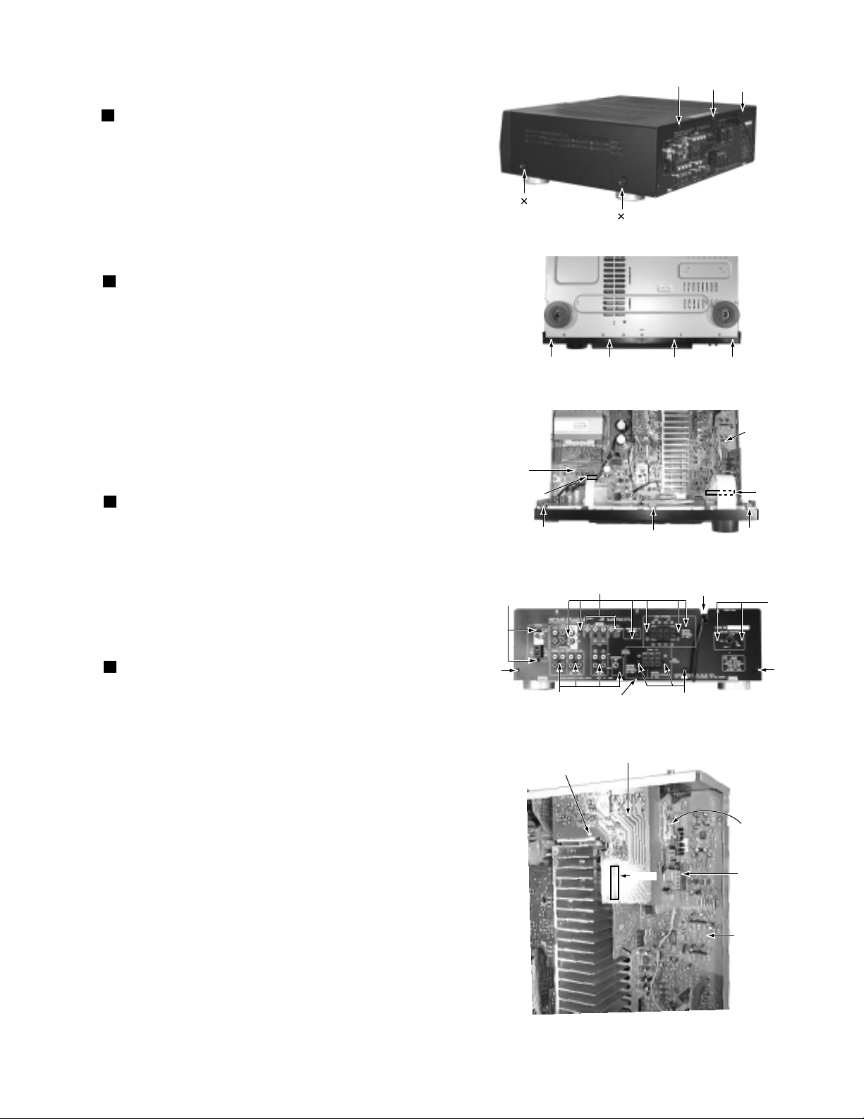
Disassembly method
Removing the top cover (See Fig.1)
1. Remove 4 screws "A" on both sides of the top cover
and 3 screws "B" on the rear side.
2. Lift the back of the top cover spreading both sides
to remove.
Removing the front panel assembly (See Fig.2,3)
1. Remove the top cover.
2. Remove 4 screws "C" on the bottom side and 3 screws
"D" on the top side.
3. Disconnect the wire CN811 on the main board.
4. Disconnect the wire CN314 on the audio & source
selector board.
5. Remove the front panel assembly.
Removing the rear panel (See Fig.4)
1. Remove the top cover.
2. Remove 21 screws "E" on the rear panel.
3. Remove 3 screws "F" on the rear panel.
4. Remove the power cord stopper up side.
5. Remove the rear panel.
Removing the tuner board and
video board (See Fig.5)
1. Remove the rear panel.
2. Remove 1 screw "G" on the video board
3. Disconnect the connector CN311 on the
video board
4. Disconnect the connector CN111 on the
audio & source selector board.
A 2
A 2
B
B
B
Fig.1
C C
C
C
Fig.2
BOTTOM COVER
Fig.4
Power cord
Stopper
E
CN311
G
VIDEO board
Fig.5
Audio &
source
selector
board
Tuner
board
CN111
D
D
D
Fig.3
CN811
CN314
Main
board
Audio &
source
selector
board
F
F
F
E
E
E
E
1-3
Page 4
RX-5000VBK/RX-5001VGD
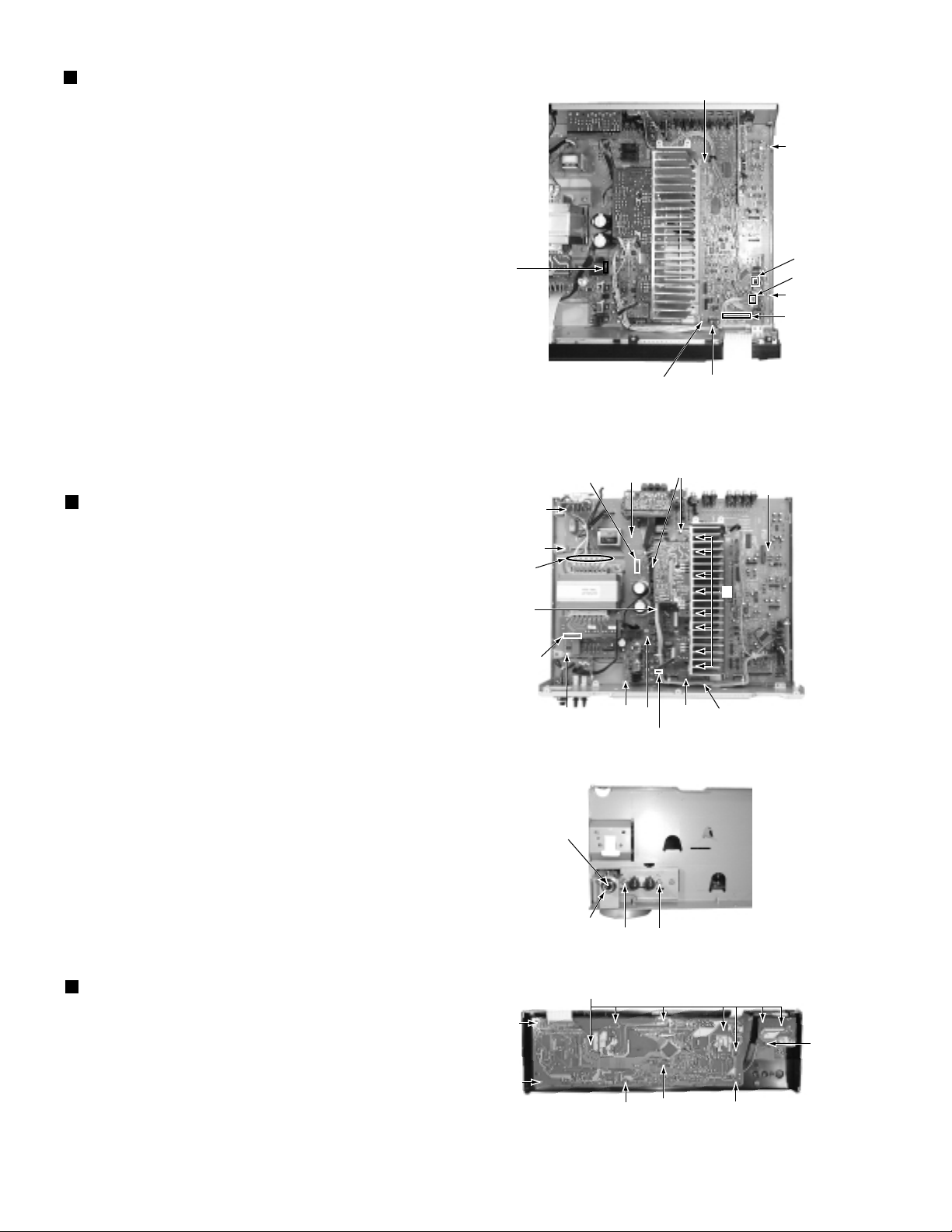
Removing the audio & source selector
board (See Fig.6)
1. Remove the rear panel.
2. Remove the video board and Tuner board.
3. Disconnect the connector CN512 and CN619 on the
audio & source selector board.
4. Disconnect to the card wire CN314 on the audio &
source selector board.
5. Disconnect the connector CN712 on the AMP board.
6. Each tie band is cut out.
7. Pullout the connection board.
8. Remove 4 screws "H" on the audio & source
selector board.
9. Remove the audio & source selector board.
Removing the main board (See Fig.6 to 8)
CN712
H
H
Audio & source
Audio & source
selector board
selector board
CN619
CN512
H
CN314
Connection board
H
Fig.6
Main
CN511
I
PCB
(Standing substrate)
I
Audio & source
selector board
1. Remove the rear panel and front panel assembly.
2. Pull out the pre AMP board and connection board.
3. Remove 8 screws "I" on the main board.
4. Remove 8 screws "J" on the power transistor.
5. Disconnect the connector CN511 and wire
CN831 on the main board.
6. Each tie band is cut out.
7. Remove 2 screws "K" on push switch of the front side.
8. Remove nut on terminal of the headphone.
9. The solder of the wire connected with the
transformer is removed.
10. Remove the main board.
Removing the front board (See Fig.9)
Solder
Pre AMP board
(Standing substrate)
Solder
Headphone jack
I
J
I
Fig.7
NUT
I
KK
L
I
CN831
I
Connection
board
Fig.8
1. Remove the top cover.
2. Remove the Front panel assembly.
3. Remove the master volume knob and nut.
4. Remove the 13 screws "L" on the Front board.
1-4
L
L
L
L
L
L
Fig.9
Page 5
Adjustment method
TUNER SECTION
1.Tuner range
FM 87.5MHz~108.0MHz
AM(MW) 530kHz~1710kHz
POWER AMPLIFIER SECTION
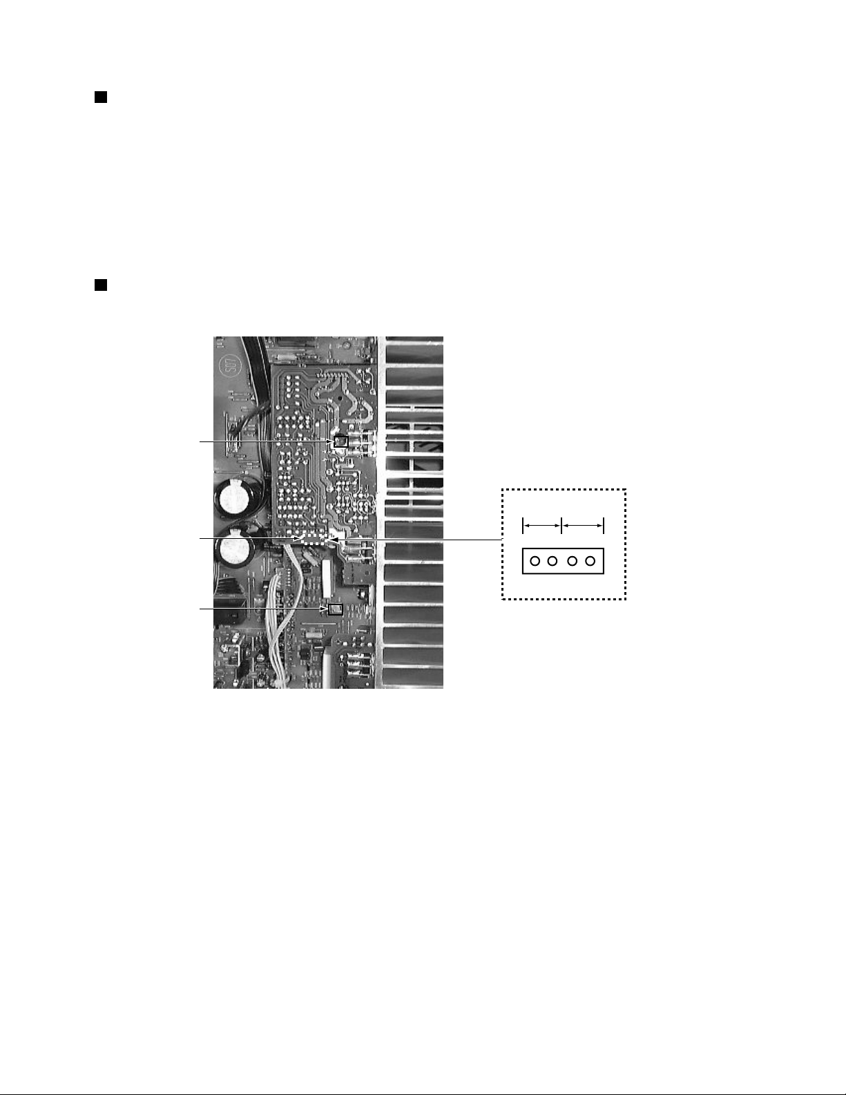
RX-5000VBK/RX-5001VGD
VR742
Rch
Lch
TP001
VR741
IDLING CURRENT
1.Set the volume control to minimum during this adjustment.
2.Set the surround mode OFF.
2.Turn VR741 and VR742 fully counterclockwise to warm up before adjustment.
If the heat sink is already warm from previous use the correct adjustment can not be made.
3.For L-ch,connect a DC voltmeter between TP001's pin1 and pin2 (Lch)
And,connect it between pin3 and pin4(Rch).
4.30 minutes later after power on, adjust VR741 for L-ch, or VR742 for R-ch so that the DC voltmeter
value has 1mV~10mV.
4 3 2 1
TP001
1-5
Page 6
RX-5000VBK/RX-5001VGD
Description of major ICs
M62446FP(IC341) : 6CH Master volume
1.Block Diagram
OUT4
OUT3
OUT2
OUT1
AVDD
SWIN
GNDS
SRin
SLin
GNDC
Cin
GNDR
Rin
GNDL
Lin
BYPASSR
BYPASSL
LTRE
LBASS3
LBASS2
LBASS1
10
11
12
13
14
15
16
17
18
19
20
21
1
2
3
4
5
6
7
8
9
OUTPUT
PORT
tone
volume
volume
volume
volume
volume
volume
MCU
I/F
tone
42
41
40
39
38
37
36
35
34
33
32
31
30
29
28
27
26
25
24
23
22
DVDD
CLK
DATA
LATCH
DGND
AGND
SWout
SRout
SLout
Cout
Rout
Lout
AVSS
CL1
CL2
CR1
CR2
RTRE
RBASS3
RBASS2
RBASS1
1-6
Page 7

2.Pin Function
RX-5000VBK/RX-5001VGD
Pin No.
1
2
3
4
5
6
7
8
9
10
11
12
13
14
15
16,17
18
19~21
22
23,24
25
26
27
28
29
30
31
32
33
34
35
36
37
38
39
40
41
42
Symbol I/O Descriptions
SURROUND
BASS BOOST
INPUT-ATT
MUTING
AVDD
SWIN
A.GND
RR IN
RL IN
A.GND
C IN
A.GND
R IN
A.GND
L IN
AVSS
L OUT
R OUT
C OUT
RL OUT
RR OUT
SW OUT
A.GND
D.GND
VOL STB
VOL DATA
VOL CLK
DVDD
O
O
O
O
I
I
I
I
I
I
-
-
-
O
-
-
I
O
I
O
O
O
O
O
O
-
-
I
I
I
-
SURROUND control terminal
BASS BOOST control terminal
Input attenuator control terminal
MUTING control terminal
Analog positive power supply terminal
SUB Woofer volume signal input terminal
Analog ground terminal
R ch volume signal input terminal for rear speaker
L ch volume signal input terminal for rear speaker
Analog ground terminal
Center volume signal input terminal
Analog ground terminal
R ch volume signal input terminal
Analog ground terminal
L ch volume signal input terminal
Non connect
Frequency adjustment terminal tone/treble
Frequency adjustment terminal tone/bass
Tone output terminal
Frequency adjustment terminal tone/bass
Frequency adjustment terminal tone/treble
Frequency adjustment terminal tone/bass
L/R volume input terminal
Tone output terminal
L/R volume input terminal
Analog negative power supply terminal
L ch output
R ch output
Center volume signal output terminal
L ch volume signal output terminal for rear speaker
R ch volume signal output terminal for rear speaker
SUB Woofer volume signal output terminal
Analog ground terminal
Digital ground terminal
Latch input terminal
Volume data input terminal
Clock input terminal for data transfer
Digital power supply terminal
1-7
Page 8

RX-5000VBK/RX-5001VGD
LA1838(IC102): FM AM IF AMP&detector, FM MPX Decoder
1. Block Diagram
30
ALC
BUFF
FM
S-METER
FM IF
1
2. Pin Function
Pin
Symbol
No.
FM IN
1
AM MIX
2
3
FM IF
AM IF
4
GND
5
6
TUNED
STEREO
7
8
VCC
9
FM DET
10
AM SD
FM VSM
11
AM VSM
12
13
MUTE
14
FM/AM
MONO/ST O
15
29
28
AM
OSC
SD
COMP
S-CLRVE
PM
DET
2
I/O
I
This is an input terminal of FM IF
REG
AM
MIX
AM/FM
IF-BUFF
3
27
FM
RF.AMP
AM IF
4
26
AGC
AM
S-METER
GND
Function
DET
5
signal.
This is an out put terminal for AM
O
mixer.
I
Bypass of FM IF
Input of AM IF Signal.
I
I
This is the device ground terminal.
When the set is tunning,this terminal
O
becomes "L".
O
Stereo indicator output. Stereo "L",
Mono: "H"
III
This is the power supply terminal.
I
FM detect transformer.
I
This is a terminal of AM ceramic filter.
O
Adjust FM SD sensitivity.
O
Adjust AM SD sensitivity.
I/O
When the signal of IF REQ of IC121(
LC72131) appear, the signal of FM/AM
IF output. //Muting control input.
Change over the FM/AM input.
I
"H" :FM, "L" : AM
Stereo : "H", Mono: "L"
25
TUNING
DRIVE
6
24
STEREO
DRIVE
7
22
23
P-DET
VCC
89
Pin
Symbol
No.
16
R OUT
17
L OUT
18
19
20
21
22
23
24
25
26
27
28
29
30
R IN
L IN
RO
LO
IF IN
FM OUT
AM DET
AM AGC
AFC
AM RF
REG
AM OSC
OSC BUFFER
21
DECODER
ANIT-BIRDIE
VCO
384KHz
10
20
STEREO
5N
SW
FF
38k
11
I/O
O
Right channel signal output.
O
Left channel signal output.
Input terminal of the Right channel post
I
18
19
MUTE
FF
/
19k
2
12 13
FF
19k
/LS
Function
17 16
PILOT
DET
14
AMP.
Input terminal of the Left channel
I
post AMP.
Mpx Right channel signal output.
O
O
Mpx Left channel signal output.
I
Mpx input terminal
FM detection output.
O
AM detection output.
O
This is an AGC voltage input terminal
I
for AM
I
This is an output terminal of voltage
for FM-AFC.
AM RF signal input.
I
Register value between pin 26 and pin28
O
besides the frequency width of the
input signal.
I
This is a terminal of AM Local
oscillation circuit.
AM Local oscillation Signal output.
O
15
1-8
Page 9

1. Pin layout
1
2
3
4
5
6
7
8
9
10
11
22
21
20
19
18
17
16
15
14
13
12
XT
FM/AM
CE
DI
CLOCK
DO
FM/ST/VCO
AM/FM
SDIN
XT
GND
LPFOUT
LPFIN
PD
VCC
FMIN
AMIN
IFCONT
IFIN
Pin
No.
1
2
3
4
5
6
7
8
9
10
11
Pin
No.
12
13
14
15
16
17
18
19
20
21
22
Symbol
XT
FM/AM
CE
DI
CLOCK
DO
FM/ST/VCO
AM/FM
LW
MW
SDIN
Symbol
IFIN
IFCONT
AMIN
FMIN
VCC
PD
LPFIN
LPFOUT
GND
XT
Function
X'tal oscillator connect (75kHz)
LOW:FM mode
When data output/input for 4pin(input) and
6pin(output): H
Input for receive the serial data from
controller
Sync signal input use
Data output for Controller
Output port
"Low": MW mode
Open state after the power on reset
Input/output port
Input/output port
Data input/output
Function
IF counter signal input
IF signal output
Not use
AM Local OSC signal output
FM Local OSC signal input
Power suplly(VDD=4.5-5.5V)
When power ON:Reset circuit move
PLL charge pump output(H: Local OSC
frequency Height than Reference frequency.
L: Low Agreement: Height impedance)
Input for active lowpassfilter of PLL
Output for active lowpassfilter of PLL
Connected to GND
X'tal oscillator(75KHz)
I/O
I
O
I
I
I
O
O
O
I/O
I/O
I/O
I/O
I
O
-
I
I
-
O
I
O
I
Reference
Driver
Phase
Detector
Charge Pump
Unlock
Detector
Universal
Counter
Swallow Counter
1/16,1/17 4bit
12bit
Programmable
DriverS
Swallow Counter
1/16,1/17 4bit
Data Shift Register & Latch
Power
on
Reset
C
2B
I/F
1/2
7821113
21
17
6
5
4
3
15
16
22
1
18
19
20
12
2. Block diagram
3. Pin function
LC72136N (IC121) : PLL Frequency Synthesizer
RX-5000VBK/RX-5001VGD
1-9
Page 10

RX-5000VBK/RX-5001VGD
MN173222BA(IC401) : System controller
1.Key Matrix
KEY OUT 0
KEY IN 0
KEY IN 1
KEY IN 2
KEY IN 3
2.Pin Function (1/2)
Pin No. Symbol
1,2
3,4
5
6
7~10
11
12~21
22
23
24~39
40
41
42
43
44
45
46
47
48
49
50
51
52
53
54
55
56
57
58
59
60
61
62
63
64
IN1,2
VIDEO1,2
PROTECT
POWER
KI0~3
VCR /S/C
G11~G2
G1/KO7
VPP
S1~16
B.BOOST LED
CLK.D
DATAIN.D
DATAOUT.D
INH
RDS CLK
RDS DATA
SW DATA
REMOCON IN
RDS D.ST
STEREO
TUNED
CE.PLL
CK.PLL
SW.CLK
DO.PLL
DCS IN
DCS OUT
ERR.DSP
IFOK.DSP
ACK.DSP
CD.DSP
RELAY Sch
T.MUTE
SUBWFMUTE
POWER
ADJUST
SETTING
MEMORY
KEY OUT1
SURROUND
ONE TOUCH
OPERATION
INPUT ATT
KEY OUT 2
DVD MULTI
DVD
VCR
FM
KEY OUT 3 KEY OUT 4
I/O Function
Volume jog signal input
I
Video signal switch output
O
Protect signal input of speaker
I
Power ON output
O
Key matrix signal input
I
Not used
FL grid signal output
O
FL grid signal output / Key matrix signal output
O
Power supply
FL segment control signal output
O
Bass boost indicator control
O
Clock signal output to DSP
O
Data signal input from DSP
I
Data signal output to DSP
O
Inhibit detection signal input
I
Clock signal input from RDS
I
Data input from RDS
I
Function switch data signal output
O
Remote control signal input
I
Data start signal for block data to output serial data
I
Stereo indicator output. Stereo "L" Mono "H"
I
When the set is tuning, this terminal becomes "L"
I
Chip enable output to IC121
O
Clock signal for IC121
I/O
Function switch clock signal output
O
Tuner PLL data
I/O
Compulink signal input
I
Compulink signal output
O
DSP control data input
I
DSP control data input
I
DSP control data input
I
DSP control data output
O
Rear ch relay control signal output
O
TUNER mute signal output
O
Sub woofer mute signal output
O
CD
PHONE
TAPE/MD
AM
1-10
Page 11
65
66
67
68
69
70
71
72
73
74
75
76
77
78
79
80
81
82
83
84
TV OUT
VCR OUT
VCR IN
RESET IN
X1
X2
VSS
OSC2
OSC1
VDD
RELAY Cch
RELAY L/R
SURROUND
INPUT ATT LED
ONE T. LED
STANDBY LED
STB-SW
VOLUME DATA
VOLUME CLK
VOLUMESTB
Pin No. Symbol
I/O Function
Connect to GND
Connect to GND
Reset signal input
Connect to GND
Non connect
Connect to GND
Oscillation terminal
Oscillation terminal
Power supply
Center ch relay control signal output
Front ch relay control signal output
Surround ON/OFF control
INPUT ATT. Indicator control
ONE TOUCH OPERATION indicator control
STANDBY indicator control
Strobe signal output of function switch
Data output to IC341
Clock signal output to IC341
Strobe signal output to IC341
-
-
I
-
-
-
-
-
-
O
O
O
O
O
O
O
O
O
O
2.Pin Function (2/2)
CTL 1
L
H
L/H
CTL 2
L
L
H
Output
VIN 1
VIN 2
VIN 3
Control input - output signal
GND
8
Vout
7
V+
6
Vin3
5
1
Vin1
2
CTL1
3
Vin2
4
CTL2
6dB
AMP.
BIAS
NJM2246D(IC201):Video Switch
RX-5000VBK/RX-5001VGD
1-11
Page 12

RX-5000VBK/RX-5001VGD
TC9471F(IC601) : Dolby prologic
1.Block Diagram
FBUS
STABUS
Timing Gen.
DBUS
OFP
CP
DLA Gen.
DFRAM
64w 16b
CRAM
320w 16b
DLRAM
DLRO DLRI
FBUS
4kw 16b
MAC Block
DBUS
SI0 register
SI1 register
SO0 register
SO2 register
SO1 register
PC Block
CRP Gen.
Lin Log Adj.
DP Gen.
CROM
256w 16b
DRAM
256w 24b
PROM
1kw 32b
FBUS
DBUS
(LDA)
IR
(JMP)
LC
(LDB)
IDEC
Self
Boot
MCU-I/F
ADC(L)
ADC(R)
DF Block
(digital Filter)
DAC(L)
DAC(R)
DAC(C)
DAC(S)
1-12
Page 13

2.Pin Function (1/2)
RX-5000VBK/RX-5001VGD
Pin No.
1
2
3
4
5
6
7
8
9
10
11
12
13
14
15
16
17
18
19
20
21
22
23
24
25~29
30
31
32
33~43
44
45.46
47
48~53
54
55
56
57
Symbol
ECKO
ECKI
A.GND
A.GND
LchOUT
V-REF1
A.5V
A.5V
V-REF2
RchOUT
A.GND
A.GND
N.C
CchOUT
V-REF3
A.5V
VRO
VRI
A.5V
V-REF4
SchOUT
NC
A.GND
D.GND
NC
D.5V
D.5V
D.GND
NC
D.GND
NC
D.5V
NC
RESET
I/O
Non connect
Amplifier input terminal for external clock input.
I
Ground terminal.(For crystal oscillator circuit)
Ground terminal.(For DAC L channel)
DAC analog signal output terminal.(L channel)
O
Reference voltage terminal.(For DAC L channel)
Power supply terminal.(For DAC L channel)
Power supply terminal.(For DAC R channel)
Reference voltage terminal.(For DAC R channel)
DAC analog signal output terminal.(R channel)
O
Ground terminal.(For DAC R channel)
Ground terminal.(For DAC C channel)
DAC analog signal output terminal.(C channel)
O
DAC analog signal output terminal with attenuator.(For C channel)
O
Reference voltage terminal.(For DAC C channel)
Power supply terminal.(For DAC C channel)
Reference voltage terminal for attenuator.(Output buffer)
O
Reference voltage terminal for attenuator.(Input buffer)
I
Power supply terminal.(For DAC S channel)
Reference voltage terminal.(For DAC S channel)
DAC analog signal output terminal with attenuator.(For S channel)
O
Non connect.
Ground terminal.(For DAC S channel)
Ground terminal.
Non connect.
Power supply terminal.
Power supply terminal.(For DLRAM)
Ground terminal.(For DLRAM)
Non connect.
Ground terminal.
Non connect.
Power supply terminal.
Non connect.
Ground terminal.
Power supply.
Ground terminal.
Power supply.
I
Function
1-13
Page 14

RX-5000VBK/RX-5001VGD
2.Pin Function (2/2)
Pin No.
58
59~71
72
73
74
75
76
77
78
79
80
81,82
83
84~87
88
89
90
91
92,93
94
95
96,97
98
99
100
Symbol
D.5V
DSP-CS
DSP-CLK
DATA-IN
DATA-OUT
DSP-IFOK
DSP-ACK
DSP-ERR
I2CS
BOOT
D.5V
D.GND
A.GND
LchIN
V-REF5
A.5V
V-REF6
RchIN
A.GND
XI
XO
A.5V
I/O
Power supply terminal
Non connect.
Chip select signal input terminal.(MCU interface)
I
Data sift clock input terminal.(MCU interface)
I
Data input terminal.(MCU interface)
I/O
At the IC bus mode,data input /output terminal.
Data output terminal.(MCU interface)
O
At the IC bus mode,normally open.
Operation flag output terminal.(MCU interface)
O
Acknowledge signal output terminal.(MCU interface)
O
Error flag output terminal.(MCU interface)
O
IC bus mode select terminal.
I
Self-boot control terminal.
I
Non connect.
Power supply terminal.
Ground terminal.
Digital ground terminal.(For ADC L channel)
Analog ground terminal.(For ADC L channel)
ADC analog signal input terminal.(L channel)
I
Reference voltage terminal.(For ADC L channel)
Analog power supply terminal.
Reference voltage terminal.(For ADC R channel)
ADC analog signal input terminal.(R channel)
Analog ground terminal.(For ADC R channel)
Crystal oscillator connection terminal.(input)
I
Crystal oscillator connection terminal.(output)
O
Power supply terminal.(For crystal oscillator circuit)
-
Function
1-14
Page 15
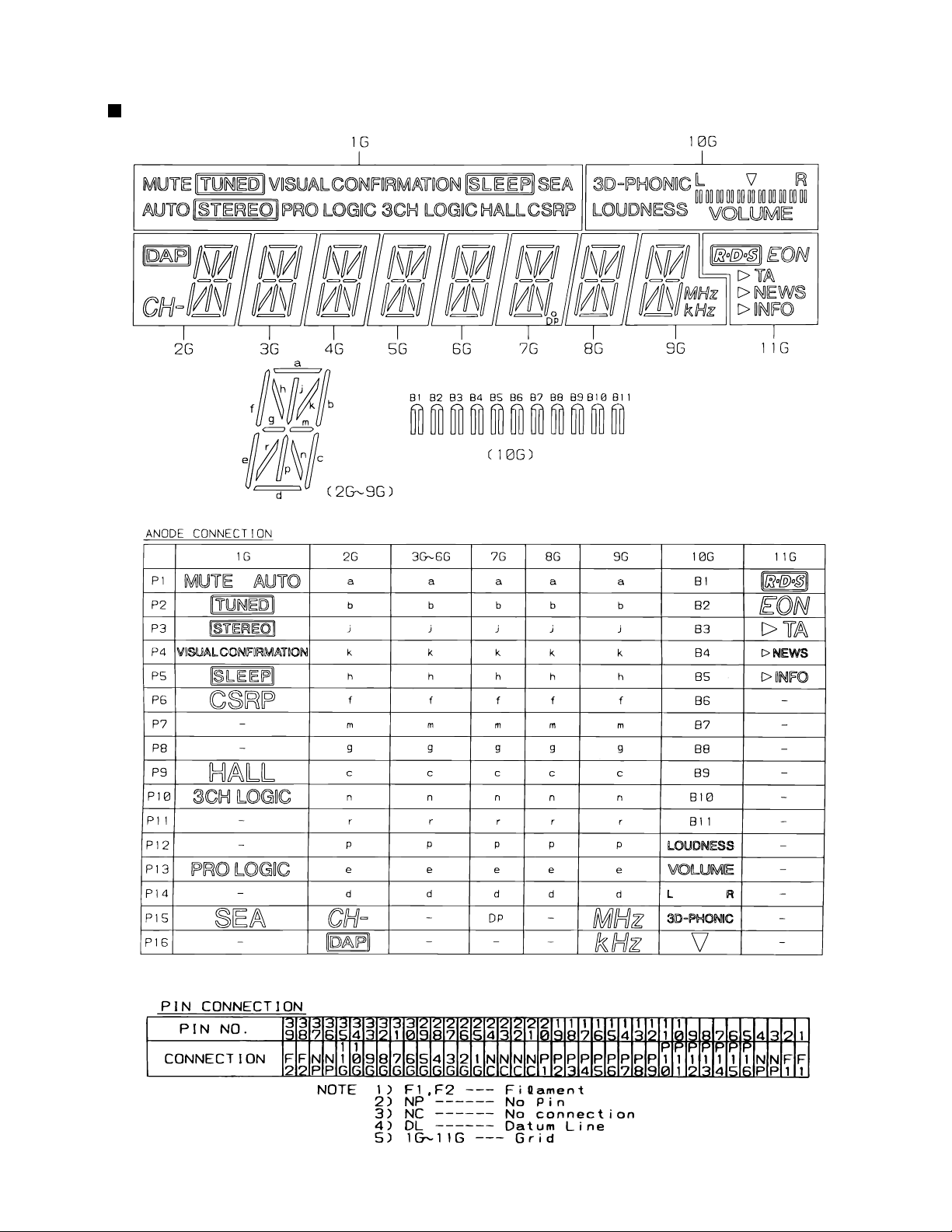
Internal connections for FL display tube
QLF0002-001(DI401):FL DISPLAY TUBE
RX-5000VBK/RX-5001VGD
1-15
Page 16

RX-5000VBK
RX-5001VGD
VICTOR COMPANY OF JAPAN, LIMITED
AUDIO & COMMUNICATION BUSINESS DIVISION
PERSONAL & MOBILE NETWORK BUSINESS UNIT. 10-1,1Chome,Ohwatari-machi,maebashi-city,371-8543,Japan
No.20883
Printed in Japan
200011(V)
 Loading...