

Page 1
YA350200511
SERVICE MANUAL
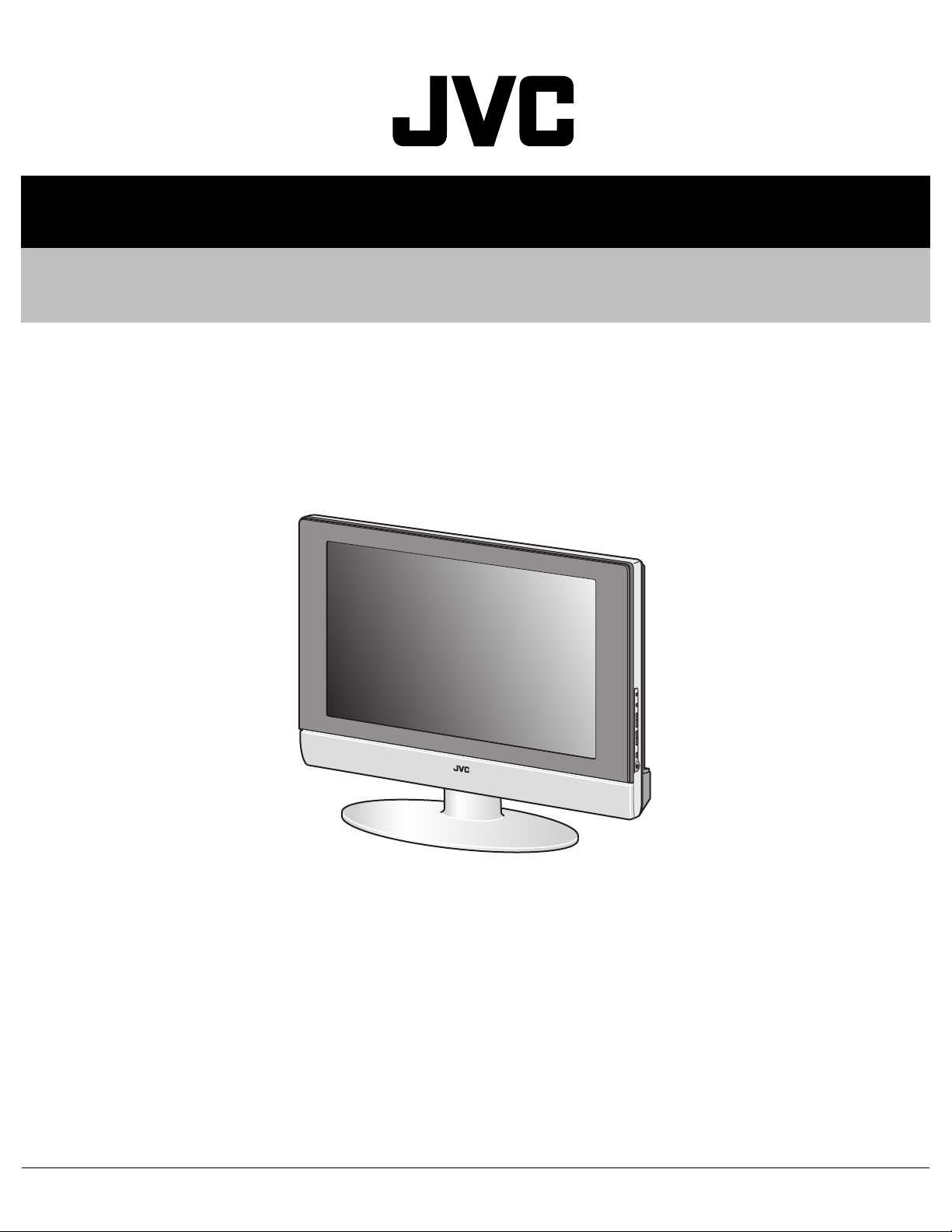
LCD FLAT TELEVISION
LT-20A5,
LT-20A5
/S
TABLE OF CONTENTS
1 PRECAUTION. . . . . . . . . . . . . . . . . . . . . . . . . . . . . . . . . . . . . . . . . . . . . . . . . . . . . . . . . . . . . . . . . . . . . . . . . 1-3
2 SPECIFIC SERVICE INSTRUCTIONS . . . . . . . . . . . . . . . . . . . . . . . . . . . . . . . . . . . . . . . . . . . . . . . . . . . . . . 1-5
3 DISASSEMBLY . . . . . . . . . . . . . . . . . . . . . . . . . . . . . . . . . . . . . . . . . . . . . . . . . . . . . . . . . . . . . . . . . . . . . . . 1-6
4 ADJUSTMENT . . . . . . . . . . . . . . . . . . . . . . . . . . . . . . . . . . . . . . . . . . . . . . . . . . . . . . . . . . . . . . . . . . . . . . . 1-19
5 TROUBLESHOOTING . . . . . . . . . . . . . . . . . . . . . . . . . . . . . . . . . . . . . . . . . . . . . . . . . . . . . . . . . . . . . . . . . 1-20
COPYRIGHT © 2005 Victor Company of Japan, Limited
No.YA350
2005/11
Page 2
SPECIFICATION
Item Contents
Dimensions (W × H × D) 54.1cm × 41.6cm × 9.2cm (TV only)
54.1cm × 47.7cm × 12.6cm (Included Stand)
Mass 9.0kg (TV only)
10.2kg (Included Stand)
TV RF System CCIR B/G, I, D/K, L
Color System PAL / SECAM / NTSC3.58 / NTSC4.43
Sound System A2 (B/G, D/K), NICAM (B/G, I, D/K), NTSC-M
Teletext System FLOF (Fastext), WST (World Standard System)
TV Receiving
Channels
Power Input TV
Power Consumption 60W (Stand-by : 1W)
LCD Panel 20.1V wide aspect (15 : 9)
Screen Size Diagonal : 51.0cm (H : 40.8cm × V : 30.6cm)
Display Pixels Horizontal : 640 pixels x Vertical : 480 pixels (VGA)
Audio Power Output 3W + 3W
Speaker 5.4cm round type × 2
Antenna Terminal 75Ω unbalanced, coaxial
Video/Audio Input [VIDEO-1]
Headphone 3.5mm mini jack × 1
Remote Control Unit RM-C1861 (AA/R6/UM-3 battery × 2)
AC Adapter DA-E061370334
VHF Low
VHF High
UHF
CATV
AC Adapter
S-Video
Video
Audio
[VIDEO-2]
Component
Video
Audio
48.25MHz ~ 158MHz
160MHz ~ 442MHz
442MHz ~ 863.25MHz
Mid : X ~ Z+2, S1 ~ S10
Super : S11 ~ S20
Hyper : S21 ~ S41
DC 12V
AC 110V ~ AC 240V, 50Hz / 60Hz
Mini-DIN 4pin × 1
Y : 1V(p-p), positive (negative sync), 75Ω
C : 0.286V(p-p), (Burst signal), 75Ω
1V(p-p), positive (negative sync), 75Ω, RCA pin jack × 1
500mV(rms), high inpedance, RCA pin jack × 2
RCA pin jack × 3
Y : 1V(p-p), positive (negative sync), 75Ω
Pb/Pr : 0.7V(p-p), 75Ω
500mV(rms), high inpedance, RCA pin jack × 2
NOTE : Design & specifications are subject to change without notice.
1-2 (No.YA350)
Page 3

SECTION 1
PRECAUTION
1.1 SAFETY PRECAUTIONS
(1) The design of this product contains special hardware,
many circuits and components specially for safety
purposes. For continued protection, no changes should be
made to the original design unless authorized in writing by
the manufacturer. Replacement parts must be identical to
those used in the original circuits. Service should be
performed by qualified personnel only.
(2) Alterations of the design or circuitry of the products should
not be made. Any design alterations or additions will void
the manufacturer's warranty and will further relieve the
manufacturer of responsibility for personal injury or
property damage resulting therefrom.
(3) Many electrical and mechanical parts in the products have
special safety-related characteristics. These characteristics
are often not evident from visual inspection nor can the
protection afforded by them necessarily be obtained by
using replacement components rated for higher voltage,
wattage, etc. Replacement parts which have these special
safety characteristics are identified in the parts list of
Service manual. Electrical components having such
features are identified by shading on the schematics
and by ( ) on the parts list in Service manual. The use
of a substitute replacement which does not have the same
safety characteristics as the recommended replacement
part shown in the parts list of Service manual may cause
shock, fire, or other hazards.
(4) Don't short between the LIVE side ground and
ISOLATED (NEUTRAL) side ground or EARTH side
ground when repairing.
Some model's power circuit is partly different in the GND.
The difference of the GND is shown by the LIVE : ( ) side
GND, the ISOLATED (NEUTRAL) : ( ) side GND and
EARTH : ( ) side GND.
Don't short between the LIVE side GND and ISOLATED
(NEUTRAL) side GND or EARTH side GND and never
measure the LIVE side GND and ISOLATED (NEUTRAL)
side GND or EARTH side GND at the same time with a
measuring apparatus (oscilloscope etc.). If above note will
not be kept, a fuse or any parts will be broken.
(5) If any repair has been made to the chassis, it is
recommended that the B1 setting should be checked or
adjusted (See ADJUSTMENT OF B1 POWER SUPPLY).
(6) The high voltage applied to the picture tube must conform
with that specified in Service manual. Excessive high
voltage can cause an increase in X-Ray emission, arcing
and possible component damage, therefore operation under
excessive high voltage conditions should be kept to a
minimum, or should be prevented. If severe arcing occurs,
remove the AC power immediately and determine the cause
by visual inspection (incorrect installation, cracked or melted
high voltage harness, poor soldering, etc.). To maintain the
proper minimum level of soft X-Ray emission, components
in the high voltage circuitry including the picture tube must
be the exact replacements or alternatives approved by the
manufacturer of the complete product.
(7) Do not check high voltage by drawing an arc. Use a high
voltage meter or a high voltage probe with a VTVM.
Discharge the picture tube before attempting meter
connection, by connecting a clip lead to the ground frame
and connecting the other end of the lead through a 10kΩ
2W resistor to the anode button.
(8) When service is required, observe the original lead dress.
Extra precaution should be given to assure correct lead
dress in the high voltage circuit area. Where a short circuit
has occurred, those components that indicate evidence of
overheating should be replaced. Always use the manufacturer's replacement components.
(9) Isolation Check (Safety for Electrical Shock Hazard)
After re-assembling the product, always perform an
isolation check on the exposed metal parts of the cabinet
(antenna terminals, video/audio input and output terminals,
Control knobs, metal cabinet, screw heads, earphone jack,
control shafts, etc.) to be sure the product is safe to operate
without danger of electrical shock.
a) Dielectric Strength Test
The isolation between the AC primary circuit and all metal
parts exposed to the user, particularly any exposed metal
part having a return path to the chassis should withstand a
voltage of 3000V AC (r.m.s.) for a period of one second. (.
. . . Withstand a voltage of 1100V AC (r.m.s.) to an
appliance rated up to 120V, and 3000V AC (r.m.s.) to an
appliance rated 200V or more, for a period of one second.)
This method of test requires a test equipment not generally
found in the service trade.
b) Leakage Current Check
Plug the AC line cord directly into the AC outlet (do not use
a line isolation transformer during this check.). Using a
"Leakage Current Tester", measure the leakage current
from each exposed metal part of the cabinet, particularly
any exposed metal part having a return path to the chassis,
to a known good earth ground (water pipe, etc.). Any
leakage current must not exceed 0.5mA AC (r.m.s.).
However, in tropical area, this must not exceed 0.2mA AC
(r.m.s.).
Alternate Check Method
Plug the AC line cord directly into the AC outlet (do not
use a line isolation transformer during this check.). Use
an AC voltmeter having 1000Ω per volt or more
sensitivity in the following manner. Connect a 1500Ω
10W resistor paralleled by a 0.15µF AC-type capacitor
between an exposed metal part and a known good earth
ground (water pipe, etc.). Measure the AC voltage
across the resistor with the AC voltmeter. Move the
resistor connection to each exposed metal part,
particularly any exposed metal part having a return path
to the chassis, and measure the AC voltage across the
resistor. Now, reverse the plug in the AC outlet and
repeat each measurement. Any voltage measured must
not exceed 0.75V AC (r.m.s.). This corresponds to
0.5mA AC (r.m.s.).
However, in tropical area, this must not exceed 0.3V AC
(r.m.s.). This corresponds to 0.2mA AC (r.m.s.).
AC VOLTMETER
(HAVING 1000 /V,
OR MORE SENSITIVITY)
0.15 F AC-TYPE
PLACE THIS PROBE
1500 10W
GOOD EARTH GROUND
ON EACH EXPOSED
ME TAL PAR T
(No.YA350)1-3
Page 4
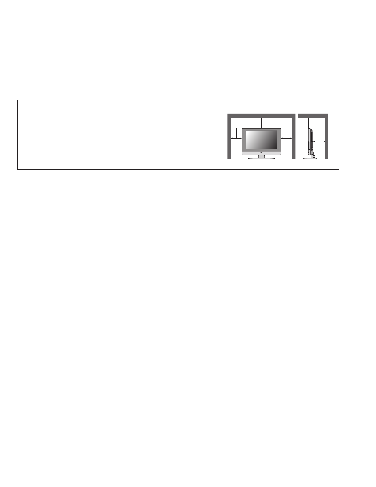
1.2 INSTALLATION
1.2.1 HEAT DISSIPATION
If the heat dissipation vent behind this unit is blocked, cooling efficiency may deteriorate and temperature inside the unit will rise.
Therefore, please make sure pay attention not to block the heat dissipation vent as well as the ventilation outlet behind the unit and
ensure that there is room for ventilation around it.
1.2.2 INSTALLATION REQUIREMENTS
Ensure that the minimal distance is maintained, as specified below, between the unit with and the surrounding walls.
Install the unit on stable flooring or stands.
Take precautionary measures to prevent the unit from tipping in order to protect against accidents and earthquakes.
Distance recommendations
Avoid improper installation and never position the unit where good ventilation
is impossible.
When installing this TV, distance recommendations must be maintained
between the set and the wall, as well as inside a tightly enclosed area or
150 mm
200 mm 200 mm
150 mm
50 mm
piece of furniture.
Keep to the minimum distance guidelines shown for safe operation.
1.3 PRECAUTIONS
(1) The picture brightness may become uneven on the entire screen according to the environmental temperature. Be sure to use
your monitor set in a specified temperature range for proper display presentation.
(2) Avoid disturbing the heat dissipation from the vent holes provided in the rear, on the top and at the sides. Failure to do so may
result in damaged electronics inside due to the accumulated heat within the unit.
(3) Be sure to install the unit in a well-ventilated place. Also make sure that the ambient temperature is kept in the range of 0 to 35°C.
(4) Avoid operation or storage in high temperature and humidity that exceed the specified limit. Otherwise, the display presentation
may be deteriorated.
(5) This monitor may display a blurred picture when exposed to an extreme environmental conditions. This phenomenon is due to
an intrinsic characteristic of the Liquid Crystal Display (LCD). This is not the failure.
(6) This monitor display uses a Cold Cathode Tube as a backlighting device. The brilliance of this tube (and the monitor display)
may be degraded by time.
1.4 CAUTIONS FOR TRANSPORTATION
The goods may be damaged during transportation caused by poor handling such as throwing, toppling, dropping, etc, giving an excess
force against the LCD device. This may happen even if the packing is rigid and secured. To avoid such adverse situations, give a
proper instruction to the freighter for secured handling. The LCD panel uses a glass plate, which is very fragile against an external
force. Take utmost care to avoid vibration or shock to the panel.
1-4 (No.YA350)
Page 5

SECTION 2
SPECIFIC SERVICE INSTRUCTIONS
2.1 ABOUT LIQUID CRYSTAL DISPLAY
2.1.1 STRUCTURE OF LIQUID CRYSTAL PANEL
The Liquid Crystal Display used for this unit is of a TFT (Thin Film Transistor) type panel. The structure of this panel is that a TFT
array-formed substrate and the stripe pixel matrix type color filter substrate are pressed together with a liquid crystal filled in between
these materials.
2.1.2 LONG-TERM AFTERIMAGE ON THE LCD
A minute amount of ionic material could be mingled into a liquid crystal substrate in the manufacturing process. By applying the
electricity to the panel the ionic material may be migrated towards one part of the electrodes, causing a long-term afterimage to be
displayed. In practice, when a still image is displayed for a long time, the afterimage may be developed and persisted. To cure this
problem, turn off the unit and then turn on again and arrange displaying an appropriate still image on the portion where the afterimage
is being superimposed.
2.1.3 RESPONSE SPEED OF THE LCD
The LCD is slower than the CRT in terms of the display refresh rate, causing a fast moving picture may be displayed blurred. This is
not fault but caused by an intrinsic characteristic of the LCD.
2.1.4 VIEWING ANGLE OF THE LCD
This LCD uses a wide-angle liquid crystal panel, featuring a low rate of the brightness inversion. When viewed from a far outer angle,
the screen may be displayed with hue variation. Again, this is not fault but caused by an intrinsic characteristic of the LCD.
2.1.5 PIXEL DEFICIENCY OF THE LCD
The liquid crystal panel is manufactured with precise engineering procedure. However, there is a possibility of yielding a little amount
of defective pixels in part on the panel. This is unavoidable feature even if the latest technology is being used for manufacturing the
LCD module.
2.2 IMPORTANT NOTICE WHEN REPLACING COMPONENT PARTS
2.2.1 REPLACING THE LCD MODULE
(1) The LCD panel is fragile against the static charge. Be sure to take an appropriate grounding using a grounding-strap etc. when
to replace the LCD panel.
(2) The LCD is made of glass, which is fragile against the mechanical shock. Use utmost care when handling the LCD panel.
(3) When replacing the panel, first place the panel on the base chassis and then make sure that there is no gap in between the panel
and the chassis. Fix the panel with fixing screws. Turn the unit on with an all-black signal being put in and check if the brightness
is even on the entire screen. If the brightness is not even in some part, slacken the fixing screw nearby until the brightness
becomes even with other parts.
(4) A tightening torque for the fixing screws must be set to 0.294Nm or the less. Applying the torque larger than this limit may result
in the damage on the LCD panel.
(5) Connecting or disconnecting the plugs with the set is being powered may cause the malfunction of the set. Makes sure that the
AC power plug is disconnected from the power source when attempting the replacement work.
2.2.2 REPLACING THE FUSE
Be sure to use the rated fuse. After replacing the fuse, confirm that the insulator is stuck on the shielding surface for secure insulation.
(No.YA350)1-5
Page 6
SECTION 3
DISASSEMBLY
3.1 DISASSEMBLY PROCEDURE
CAUTION:
• Prior to disassembly, unplug the power cord and AC
adapter from the AC outlet without fail. (Turn the power
"off".)
• When exchanging parts etc. with the front side (LCD
side) facing down, please place a protection sheet
below before starting, so as to prevent scratches on the
front side.
A x4
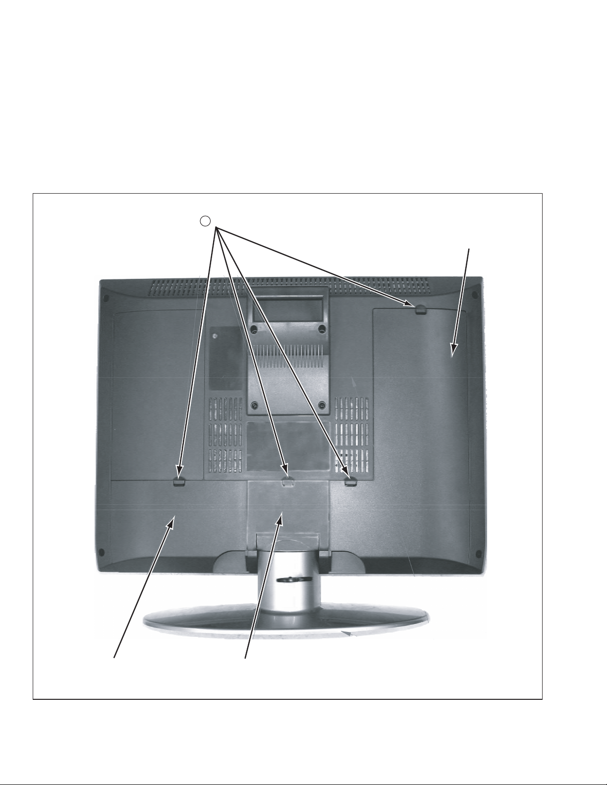
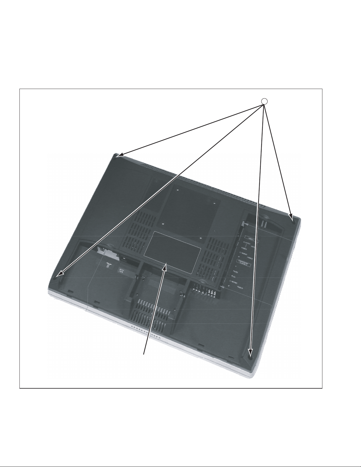
3.1.1 REMOVING THE CABLE COVER (L/R) AND NECK
COVER (Fig.1)
(1) Remove the 4 claws [A].
(2) Remove the CABLE COVER (L), CABLE COVER (R) and
NECK COVER.
CABLE COVER (L)
CABLE COVER (R) NECK COVER
1-6 (No.YA350)
Fig.1
Page 7

3.1.2 REMOVING THE STAND ASS'Y (Fig.2)
• Remove the NECK COVER.
(1) Remove the 4 screws [B] and remove the STAND ASS’Y.
3.1.3 REMOVING THE TUNER MODULE (Fig.2)
• Remove the CABLE COVER (R).
(1) Remove the DUMMY COVER by pulling the claw [C].
(2) Remove the 1 claw [C] and remove the TUNER COVER.
(3) Remove the TUNER MODULE by pulling carefully.
3.1.4 REMOVING THE AV JACK MODULE (Fig.2)
• Remove the CABLE COVER (L).
(1) Loosen the 2 screws [D].
(2) Remove the AV JACK MODULE by pulling carefully.
Dx2
DUMMY COVER
C
TUNER COVER
Bx4
TUNER
MODULE
STAND ASS'Y
AV JACK MODULE
Fig.2
(No.YA350)1-7
Page 8
3.1.5 REMOVING THE REAR COVER (Fig.3)
• Remove the CABLE COVER (L/R) and NECK COVER.
• Remove the STAND ASS’Y.
• Remove the TUNER MODULE.
• Remove the AV JACK MODULE.
(1) Remove the 4 screws [E] and remove the REAR COVER.
CAUTION:
• For the REAR COVER is attached tightly, it is easy to
open from the corner of the REAR COVER.
Ex4
1-8 (No.YA350)
REAR COVER
Fig.3
Page 9
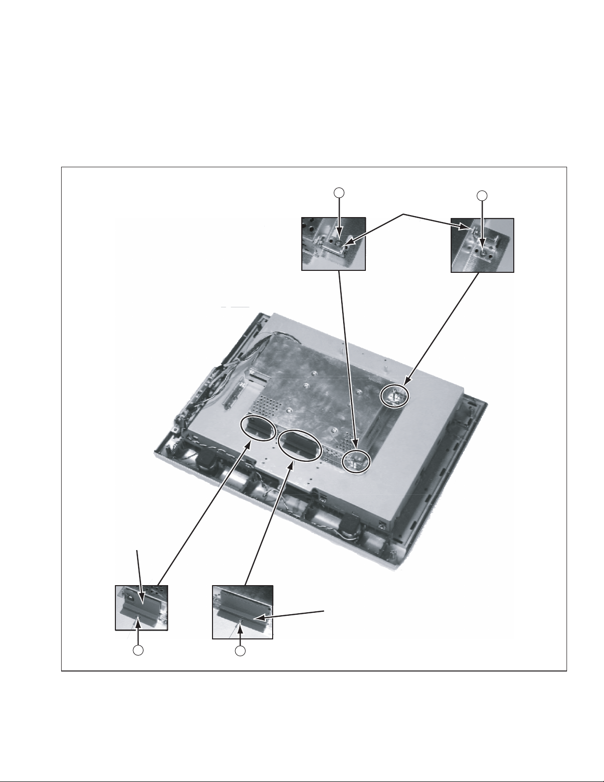
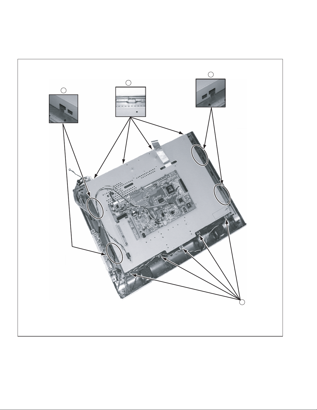
3.1.6 REMOVING THE MAIN PWB SHIELD (Fig.4, 5)
• Remove the REAR COVER.
(1) Remove the 1 screw [F] and remove the D-SUB COVER.
(Fig.4)
(2) Remove the 1 screw [G] and remove the AUDIO COVER.
(Fig.4)
(3) Remove the 2 screws [H] and remove the MODULE
BRACKETS. (Fig.4)
(4) Remove the 4 screws [I]. (Fig.5)
(5) Remove the MAIN PWB SHIELD by sliding to downside.
(Fig.5)
H
MODULE
H
BRACKET
D-SUB
COVER
F
AUDIO COVER
G
Fig.4
(No.YA350)1-9
Page 10
Ix2
MAIN PWB
SHIEELD
1-10 (No.YA350)
Ix2
Fig.5
Page 11
3.1.7 REMOVING THE MAIN PWB (Fig.6)
• Remove the REAR COVER.
• Remove the MAIN PWB SHIELD.
(1) Remove the 1 screw [J].
(2) Disconnect the connectors [P004] / [P006] / [P009] / [P017]
from the MAIN PWB.
(3) Disconnect the connector [P613] from the FRONT
CONTROL PWB.
(4) Remove the 6 screws [K] and remove the MAIN PWB.
NOTE:
• EIt is advisable to take note of the connecting location
(connector number) of the removed connectors.
[P004]
[P006]
[P009]
[P017]
J
MAIN PWB
FRONT
CONTROL
PWB
Kx6
[P613]
Fig.6
(No.YA350)1-11
Page 12
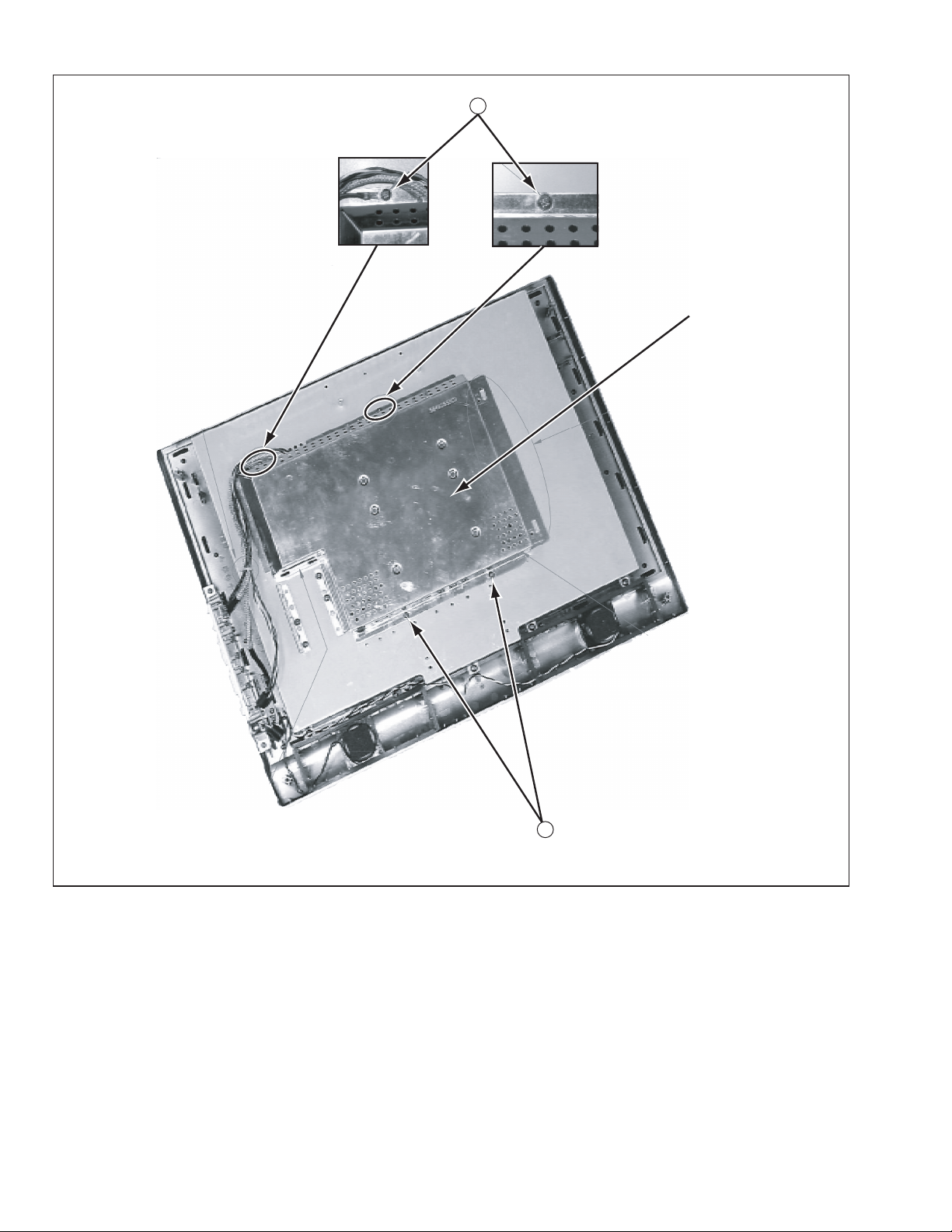
3.1.8 REMOVING THE LCD PANEL UNIT (Fig.7, 8)
• Remove the REAR COVER.
• Remove the MAIN PWB SHIELD.
• Remove the MAIN PWB.
M x2
(1) Remove the 5 screws [L]. (Fig.7)
(2) Remove the 2 claws [M], 4 claws [N] and 2 claws [O] and
remove the LCD PANEL UNIT and LCD BRACKET. (Fig.7)
(3) Remove the 4 screws [P] and remove LCD BRACKET.
(Fig.8)
Ox2
Nx4
1-12 (No.YA350)
Lx5
Fig.7
Page 13
x2
P
LCD BRACKET
Px2
Fig.8
(No.YA350)1-13
Page 14
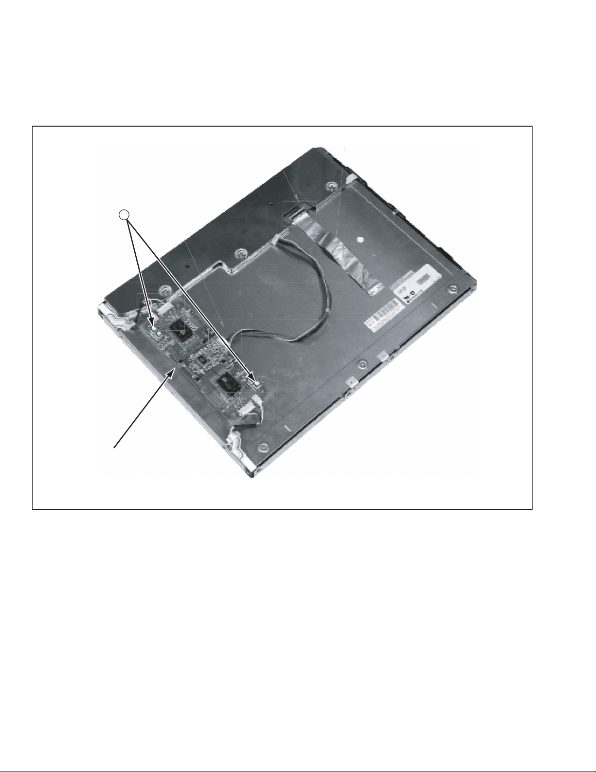
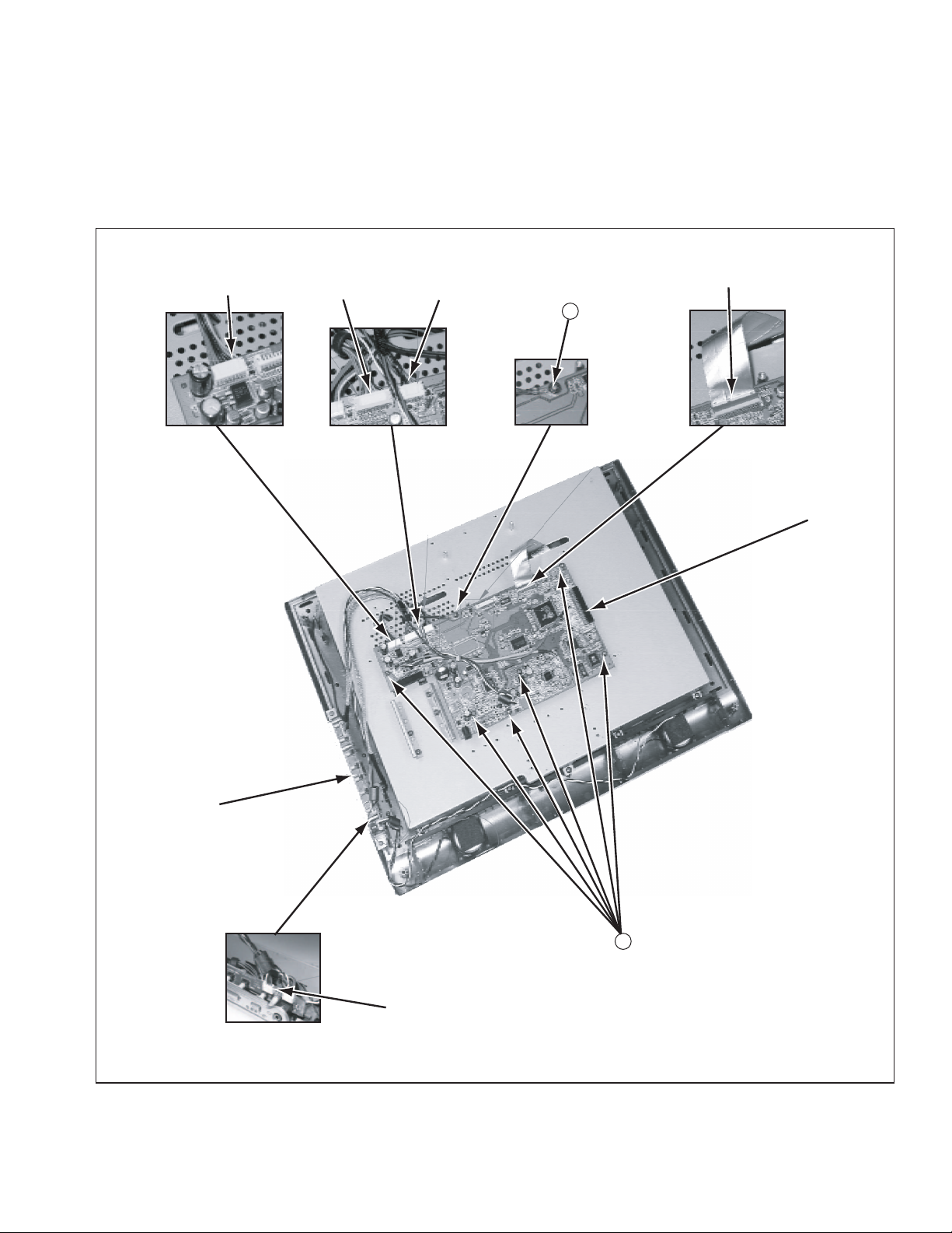
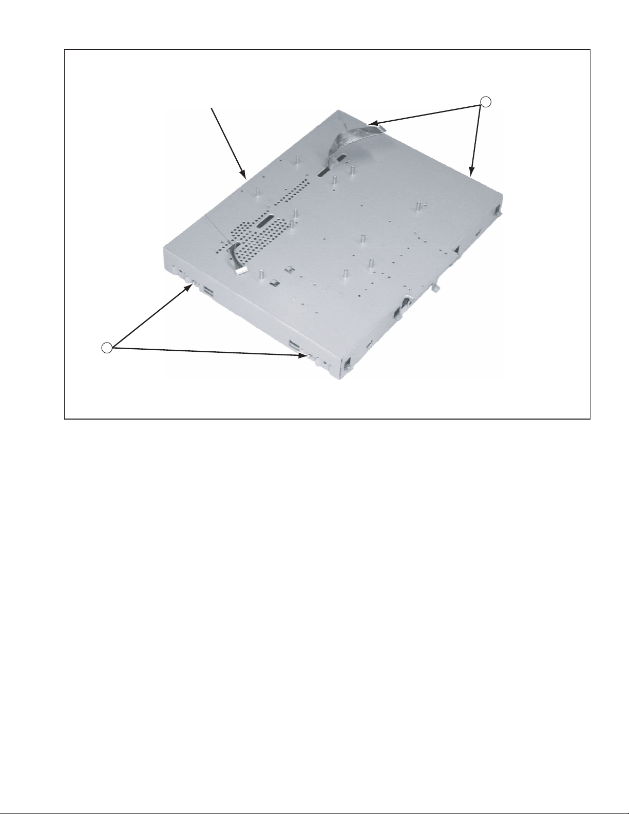
3.1.9 REMOVING THE INVERTER PWB (Fig.9)
• Remove the REAR COVER.
• Remove the MAIN PWB SHIELD.
• Remove the MAIN PWB.
• Remove the LCD BRACKET.
Qx4
(1) Remove the 2 screws [Q].
(2) Disconnect the connectors from the INVERTER PWB and
remove the INVERTER PWB.
NOTE:
• It is advisable to take note of the connecting location
(connector number) of the removed connectors.
INVERTER PWB
Fig.9
1-14 (No.YA350)
Page 15
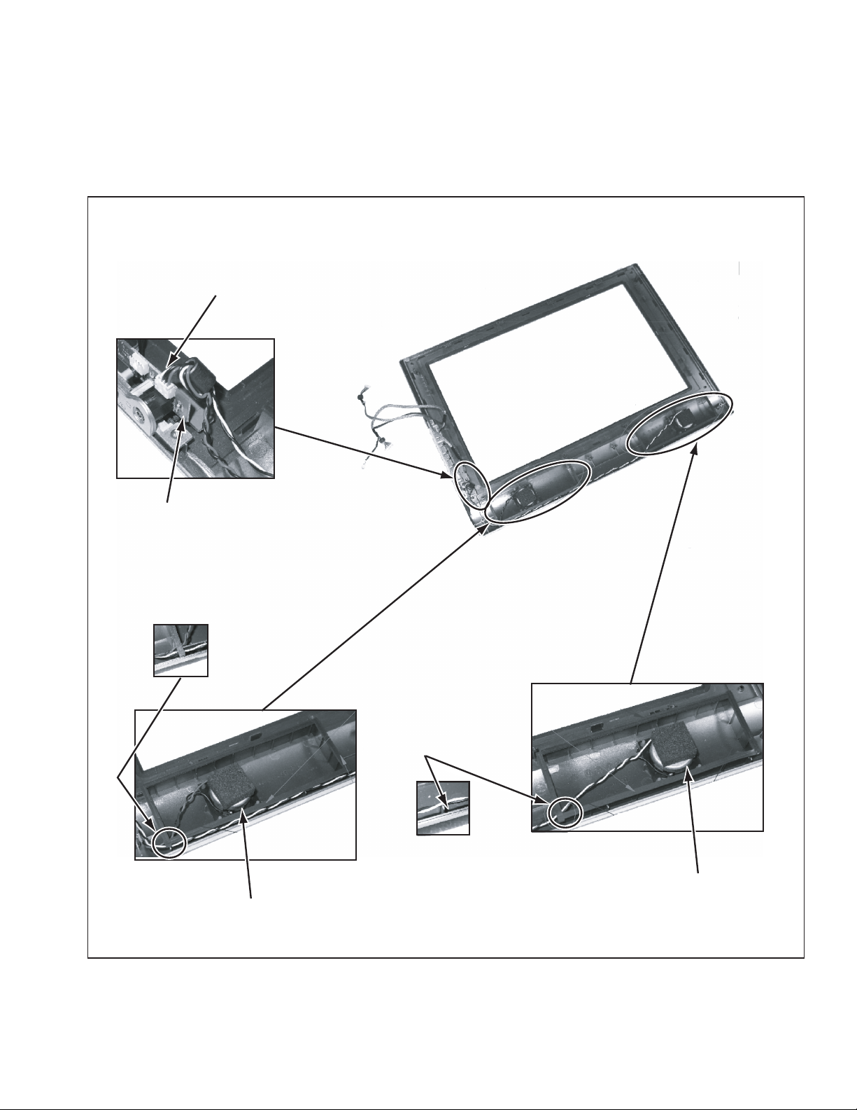
3.1.10 REMOVING THE SPEAKERS (Fig.10)
• Remove the REAR COVER.
(1) Disconnect the connector [P612] from the FRONT
CONTROL PWB.
(2) Strip off the sponges and remove the SPEAKERS.
NOTE:
• It is advisable to take note of the connecting location
(connector number) of the removed connectors.
[P612]
FRONT CONTROL PWB
SPONGE
SPEAKER
SPONGE
SPEAKER
Fig.10
(No.YA350)1-15
Page 16

3.1.11 REMOVING THE FRONT CONTROL PWB (Fig.11)
• Remove the REAR COVER.
(1) Disconnect the connector [P611] from the FRONT
CONTROL PWB.
(2) Remove the 2 screws [R].
(3) Remove the 3 screws [S] and remove the FRONT CON-
TROL PWB.
NOTE:
• EIt is advisable to take note of the connecting location
(connector number) of the removed connectors.
Rx2
3.1.12 REMOVING THE IR SENSOR PWB (Fig.11)
• Remove the REAR COVER.
(1) Remove the 1 screw [T].
(2) Disconnect the connector [P005] from the IR SENSOR
PWB.
NOTE:
• It is advisable to take note of the connecting location
(connector number) of the removed connectors.
Sx3
[P611]
T
FRONT CONTROL PWB
[P005]
IR SENSOR PWB
Fig.11
1-16 (No.YA350)
Page 17

3.2 FIRMWARE VERSION CHECK
3.2.1 PROCEDURE FOR FIRMWARE VERSION CHECK
(1) Press the [MUTING] key and the [DISPLAY] key
simultaneously, and the FACTORY MODE screen Fig.1
will be displayed.
(2) The FIRMWARE VERSION is displayed in the upperleft on
the FACTORY MODE screen.
(3) Press the [POWER] key or the [BACK] key to exit the
FACTORY MODE.
CAUTION:
• Do not change setting values of FACTORY MODE
screen.
3.2.2 SERVICE CONTROL KEY LAYOUT ON THE REMOTE CONTROL UNIT
FACTORY MODE SCREEN
FIRMWARE Ver.
Build Date:Fab 16 2005 Time:20:52:58
V23JLBJ F/W Ver. 3.83
Factory Mode
PICTURE
ADC
TCD3
Scalar
Display
Color Process
: SELECT
OK : OPERATE
NUTING
POWER
DISPLAY BACK
(No.YA350)1-17
Page 18

3.3 REPLACEMENT OF CHIP COMPONENT
3.3.1 CAUTIONS
(1) Avoid heating for more than 3 seconds.
(2) Do not rub the electrodes and the resist parts of the pattern.
(3) When removing a chip part, melt the solder adequately.
(4) Do not reuse a chip part after removing it.
3.3.2 SOLDERING IRON
(1) Use a high insulation soldering iron with a thin pointed end of it.
(2) A 30w soldering iron is recommended for easily removing parts.
3.3.3 REPLACEMENT STEPS
1. How to remove Chip parts
2. How to install Chip parts
[Resistors, capacitors, etc.]
(1) As shown in the figure, push the part with tweezers and
alternately melt the solder at each end.
(2) Shift with the tweezers and remove the chip part.
[Transistors, diodes, variable resistors, etc.]
(1) Apply extra solder to each lead.
SOLDER
SOLDER
[Resistors, capacitors, etc.]
(1) Apply solder to the pattern as indicated in the figure.
(2) Grasp the chip part with tweezers and place it on the
solder. Then heat and melt the solder at both ends of the
chip part.
[Transistors, diodes, variable resistors, etc.]
(1) Apply solder to the pattern as indicated in the figure.
(2) Grasp the chip part with tweezers and place it on the
solder.
(3) First solder lead A as indicated in the figure.
(2) As shown in the figure, push the part with tweezers and
alternately melt the solder at each lead. Shift and remove
the chip part.
NOTE :
After removing the part, remove remaining solder from the
pattern.
1-18 (No.YA350)
A
B
C
(4) Then solder leads B and C.
A
B
C
Page 19

SECTION 4
ADJUSTMENT
This service manual does not describe ADJUSTMENT.
(No.YA350)1-19
Page 20

SECTION 5
TROUBLESHOOTING
Picture
shows
MCU(I016)
hangs
End
Next
Reset the MCU(I016)
by pushing the power
key or replugging the
power cord
Replace I016
End
Still no
picture
No picture appear
Does the LED
light up
No
LED light to
amber
No
Is it entering into
power saving mode
Restart PC signal
to ensure H. V. sync
are not absens
End
Yes
Yes
Yes
No
The voltage of
L021, L022 is 12V
The voltage of
I007 1pin is 12V
The voltage of
I007 2pin is 5V
The voltage of
I016 27pin, 62pin
and 80pin is 5V
Yes
Yes
Yes
Yes
Replace I016
No
No
No
No
Check I016 socket is
Replace F001
Replace
L021 & L022
Replace
I007 & D002
loosened
Next
Yes
Yes
Yes
Yes
Yes
No
No
No
No
No
No
Replace I025
Replace I009
Replace I028
Replace I001
Replace I004
Replace I003
The voltage of
I025 2pin is 3.3V
The voltage of
I009 2pin is 3.3V
The voltage of
I028 2pin is 2.5V
The voltage of
I001 2pin is 5V
The voltage of
I004 2pin is 1.8V
The voltage of
I003 2pin is 1.8V
The H. or V. sync
does not hold
Are the output of
I037(CLK, H, V, DE)
is normal
No
Are the input
waveforms of I037
is normal
Yes
Replace I037
Yes Yes
Are flex cable
attached firmly
at P014
No
Tighten two flex
cables at P014
End
Are flex cable
attached firmly at
the LCD panel
connectors
Yes
Replace LCD panel
End
No
Tighten flex cable
at P014
End
Yes
The voltage of
I019 2pin is 3.3V
Yes
Replace I037
End
No
Replace I019
1-20 (No.YA350)
End
Page 21

(No.YA350)1-21
Page 22

Victor Company of Japan, Limited
AV & MULTIMEDIA COMPANY DISPLAY CATEGORY 12, 3-chome, Moriya-cho, Kanagawa-ku, Yokohama-city, Kanagawa-prefecture, 221-8528, Japan
(No.YA350)
Printed in Japan
VPT
Page 23

PARTS LIST
CAUTION
J The parts identified by the symbol are important for the safety . Whenever replacing these parts, be sure to use specified ones to secure the
safety.
J The parts not indicated in this Parts List and those which are filled with lines --- in the Parts No. columns will not be supplied.
J P.W. BOARD Ass'y will not be supplied, but those which are filled with the Parts No. in the Parts No. columns will be supplied.
ABBREVIATIONS OF RESISTORS, CAPACITORS AND TOLERANCES
RESISTORS CAPACITORS
CR Carbon Resistor C CAP. Ceramic Capacitor
FR Fusible Resistor E CAP. Electrolytic Capacitor
PR Plate Resistor M CAP. Mylar Capacitor
VR Variable Resistor CH CAP. Chip Capacitor
HV R High Voltage Resistor HV CAP. High Voltage Capacitor
MF R Metal Film Resistor MF CAP. Metalized Film Capacitor
MG R Metal Glazed Resistor MM CAP. Metalized Mylar Capacitor
MP R Metal Plate Resistor MP CAP. Metalized Polystyrol Capacitor
OM R Metal Oxide Film Resistor PP CAP. Polypropylene Capacitor
CMF R Coating Metal Film Resistor PS CAP. Polystyrol Capacitor
UNF R Non-Flammable Resistor TF CAP. Thin Film Capacitor
CH V R Chip Variable Resistor MPP CAP. Metalized Polypropylene Capacitor
CH MG R Chip Metal Glazed Resistor TAN. CAP. Tantalum Capacitor
COMP. R Composition Resistor CH C CAP. Chip Ceramic Capacitor
LPTC R Linear Positive Temperature Coefficient Resistor BP E CAP. Bi-Polar Electrolytic Capacitor
CH AL E CAP. Chip Aluminum Electrolytic Capacitor
CH AL BP CAP. Chip Aluminum Bi-Polar Capacitor
CH TAN. E CAP. Chip Tantalum Electrolytic Capacitor
CH AL BP E CAP. Chip Tantalum Bi-Polar Electrolytic Capacitor
RESISTORS
FGJ KMNRHZ P
±1% ±2% ±5% ±10% ±20% ±30%
+30%
-10%
+50%
-10%
+80%
-20%
+100%
-0%
(No.YA350)3-1
Page 24

CONTENTS
USING P.W. BOARD & REMOTE CONTROL UNIT ................................................................................................... 3-2
EXPLODED VIEW PARTS LIST ................................................................................................................................. 3-3
EXPLODED VIEW ....................................................................................................................................................... 3-4
PRINTED WIRING BOARD PARTS LIST ................................................................................................................... 3-5
MAIN P.W. BOARD ASS'Y DA-5098801027 (PWB-0915-PART A-01) ............................................................. 3-5
IR SENSOR P.W. BOARD ASS'Y DA-5098801028 (PWB-0915-PART B-01) .................................................. 3-8
AV JACK P.W. BOARD ASS'Y DA-098801029 (PWB-0916-PART B-01) ......................................................... 3-8
FRONT CONTROL P.W. BOARD ASS'Y DA-5098801032 (PWB-0916-PART B-01) ....................................... 3-9
TUNER P.W. BOARD ASS'Y DA-5098801030 (PWB-0916-PART C-01) ......................................................... 3-9
PACKING ................................................................................................................................................................... 3-10
PACKING PARTS LIST ............................................................................................................................................. 3-10
USING P.W. BOARD & REMOTE CONTROL UNIT
P.W.B ASS'Y LT-20A5 LT-20A5/S
MAIN P.W.B DA-5098801027 (PWB-0915-PART A-01) ←
IR SENSOR P.W.B DA-5098801028 (PWB-0915-PART B-01) ←
AV JACK P.W.B DA-5098801029 (PWB-0916-PART A-01) ←
FRONT CONTROL P.W.B DA-5098801032 (PWB-0916-PART B-01) ←
TUNER P.W.B DA-5098801030 (PWB-0916-PART C-01) ←
INVERTER P.W.B DA-E053910013 ←
REMOTE CONTROL UNIT DA-E052731049 ←
3-2(No.YA350)
Page 25

EXPLODED VIEW PARTS LIST
Ref.No. Part No. Part Name Description Local
1 DA-E642204400 FRONT COVER
2 DA-E642204302 FRONT COVER MASK
3 DA-E642440500 JVC MARK
4 DA-5642026411 SP SPONGE (x2)
5 DA-E642025603 HIGH DENSITY SPONGE (x2)
6 DA-E642026500 SPEAKER RUBBER (x8)
7 DA-E055125200 SPEAKER SP01, SP02(x2)
8 DA-E640331800 LED LENS
9 DA-E640331900 IR LENS
10 DA-E642850600 KEY
11 DA-E642319500 KEY COVER
12 DA-E051253679 LCD PANEL UNIT
13 DA-E053910013 INVERTER PWB
14 DA-E648745900 LCD BRACKET
15 DA-E646255501 MAIN PWB SHIELD
16 DA-E648742300 MODULE BRACKET (x2)
17 DA-E648742200 TUNER BRACKET (x2)
18 DA-E642318710 TUNER COVER
19 DA-E642318810 D-SUB COVER
20 DA-E642435300 D-SUB DUMMY COVER
21 DA-E642318910 AUDIO COVER
22 DA-E642438600 AUDIO DUMMY COVER
23 DA-E648731701 VISA BRACKET
24 DA-E642204500 REAR COVER
25 DA-E642901116 HANDLE
26 DA-E642323100 CABLE COVER (L)
27 DA-E642323000 CABLE COVER (R)
28 DA-E641415112 NECK COVER
29 DA-E642655800 AV JACK PWB SHIELD
30 DA-E642679610 AV JACK PWB COVER
31 DA-5095854608 STAND ASS'Y Inc. No.32 - No.34
32 DA-E642025401 RUBBER FOOT (x5)
33 DA-E642679300 CABLE HOLDER
34 DA-E641414901 HINGE COVER
35 DA-E642425400 TUNER LABEL
36 DA-E642435000 DC IN LABEL
37 DA-E642438700 AUDIO LABEL
38 DA-E642429400 I/O LABEL
39 DA-E030571128 RATING LABEL LT-20A5
39 DA-E030571129 RATING LABEL LT-20A5/S
S1 DA-G190562305 SCREW M3 x 5mm(x4)
S2 DA-G000311032 SCREW M3 x 6mm(x9)
S3 DA-G136160652 SCREW M3 x 6mm(x10)
S4 DA-G136160652 SCREW M3 x 6mm(x2)
S5 DA-G134161182 SCREW M3 x 8mm(x6)
S6 DA-G134251482 SCREW M4 x 10mm(x5)
S7 DA-G134251682 SCREW M4 x 12mm(x4)
S8 DA-G190540084 SCREW M4 x 16mm(x4)
S9 DA-E640228300 SCREW (x2)
S10 DA-G134251456 SCREW M4 x 10mm(x4)
50 DA-5098801027 MAIN PWB
51 DA-5098801028 IR SENSOR PWB
52 DA-5098801029 AV JACK PWB
53 DA-5098801032 FRONT CONTROL PWB
54 DA-5098801030 TUNER PWB
(No.YA350)3-3
Page 26

EXPLODED VIEW
27
38
S9
S7
S10
39
S5
25
30
29
24
28
26
52
37
36
S4
S8
35
16
S3
15
34
23
33
S3
21
22
S3
32
31
18
54
19
20
S2
50
17
S6
14
13
S2
3-4(No.YA350)
S1
12
7
11
S5
51
10
S5
53
5
6
4
1
2
8
3
9
Page 27

PRINTED WIRING BOARD PARTS LIST
MAIN P.W. BOARD ASS'Y
DA-5098801027 (PWB-0915-PART A-01)
Ref No. Part No. Part Name Description Local
I001 DA-F640031025 IC AP1084KA-ADJ
I002 DA-F626110018 IC SI4435BDY
I003 DA-F640031025 IC AP1084KA-ADJ
I004 DA-F640031014 IC LT1117S18
I005 DA-F640000355 IC LM3485
I006 DA-F626110018 IC SI4435BDY
I009 DA-F640010150 IC LT1117S33
I010 DA-F626110018 IC SI4435BDY
I013 DA-F647026154 IC
I015 DA-F647310702 IC W24257AJ-8N
I016 DA-F647073054 IC M30620SPGP
I021 DA-F626110018 IC SI4435BDY
I023 DA-F647026450 IC BR24L64F-W
I024 DA-F640000958 IC HT7044A
I025 DA-F640010150 IC LT1117S33
I027 DA-F644051155 IC TPA1517DWP
I028 DA-F640010159 IC LT1117S25
I031 DA-F644001350 IC THC63LVDF84A-G
I032 DA-F647014558 IC K4D263238F
I033 DA-F646036751 IC MSP3450G
I034 DA-F640000655 IC PJ78M09
I035 DA-F626090068 IC NDC7002N
I036 DA-F626090068 IC NDC7002N
I037 DA-F647003352 IC SVP-EX52-L
Q001 DA-F622010011 TRANSISTOR MMBT3904
Q002 DA-F622010011 TRANSISTOR MMBT3904
Q003 DA-F622010011 TRANSISTOR MMBT3904
Q004 DA-F622010011 TRANSISTOR MMBT3904
Q005 DA-F622010011 TRANSISTOR MMBT3904
Q006 DA-F623010011 TRANSISTOR MMBT3906
Q007 DA-F623010011 TRANSISTOR MMBT3906
Q009 DA-F622010011 TRANSISTOR MMBT3904
Q010 DA-F623010011 TRANSISTOR MMBT3906
Q011 DA-F623010011 TRANSISTOR MMBT3906
Q013 DA-F622010011 TRANSISTOR MMBT3904
Q015 DA-F623010011 TRANSISTOR MMBT3906
Q042 DA-F622010011 TRANSISTOR MMBT3904
D005 DA-F611020036 DIODE B340
D018 DA-F613020019 DIODE LL4148
D022 DA-F613020019 DIODE LL4148
D024 DA-F613020019 DIODE LL4148
D025 DA-F613020019 DIODE LL4148
D026 DA-F613020019 DIODE LL4148
D028 DA-F613020019 DIODE LL4148
ZD15 DA-F615010091 Z DIODE BZT52C3V6
C001 DA-E230003391 CAPACITOR 0.1uF 25V Z
C003 DA-E216029302 CAPACITOR 330uF 35V
C004 DA-E230003391 CAPACITOR 0.1uF 25V Z
C005 DA-E218027093 CAPACITOR 100uF 16V M
C007 DA-E218027093 CAPACITOR 100uF 16V M
C008 DA-E230003391 CAPACITOR 0.1uF 25V Z
C009 DA-E218027093 CAPACITOR 100uF 16V M
C010 DA-E230003391 CAPACITOR 0.1uF 25V Z
C011 DA-E230003391 CAPACITOR 0.1uF 25V Z
C012 DA-E218027093 CAPACITOR 100uF 16V M
C013 DA-E240610191 CAPACITOR 100pF 50V J
C014 DA-E240610191 CAPACITOR 100pF 50V J
C015 DA-E240610191 CAPACITOR 100pF 50V J
C016 DA-E240610191 CAPACITOR 100pF 50V J
C017 DA-E240610191 CAPACITOR 100pF 50V J
C020 DA-E240610191 CAPACITOR 100pF 50V J
C022 DA-E240610191 CAPACITOR 100pF 50V J
C024 DA-E218027093 CAPACITOR 100uF 16V M
C025 DA-E230003391 CAPACITOR 0.1uF 25V Z
C027 DA-E218027093 CAPACITOR 100uF 16V M
C028 DA-E230003391 CAPACITOR 0.1uF 25V Z
C029 DA-E218027093 CAPACITOR 100uF 16V M
C030 DA-E240610191 CAPACITOR 100pF 50V J
C031 DA-E230003391 CAPACITOR 0.1uF 25V Z
C032 DA-E230003391 CAPACITOR 0.1uF 25V Z
C034 DA-E230003391 CAPACITOR 0.1uF 25V Z
C035 DA-E216029302 CAPACITOR 330uF 35V
C037 DA-E218027093 CAPACITOR 100uF 16V M
C039 DA-E230003391 CAPACITOR 0.1uF 25V Z
C043 DA-E250810591 CAPACITOR 1uF 25V Z
C044 DA-E230003391 CAPACITOR 0.1uF 25V Z
C045 DA-E218027093 CAPACITOR 100uF 16V M
SST39SF040-70-4C-NHM
Ref No. Part No. Part Name Description Local
C046 DA-E216028903 CAPACITOR 470uF 25V M
C048 DA-E216028903 CAPACITOR 470uF 25V M
C054 DA-E218007993 CAPACITOR 100uF 16V M
C106 DA-E230003391 CAPACITOR 0.1uF 25V Z
C110 DA-E218007993 CAPACITOR 100uF 16V M
C111 DA-E240647091 CAPACITOR 47pF 50V J
C112 DA-E218008893 CAPACITOR 22uF 16V M
C113 DA-E230003391 CAPACITOR 0.1uF 25V Z
C115 DA-E230003391 CAPACITOR 0.1uF 25V Z
C116 DA-E216028903 CAPACITOR 470uF 25V M
C119 DA-E240647091 CAPACITOR 47pF 50V J
C120 DA-E230003391 CAPACITOR 0.1uF 25V Z
C121 DA-E230019191 CAPACITOR 0.15uF DC 16V Z
C122 DA-E218007993 CAPACITOR 100uF 16V M
C124 DA-E230003391 CAPACITOR 0.1uF 25V Z
C126 DA-E216028903 CAPACITOR 470uF 25V M
C127 DA-E230014191 CAPACITOR 2.2uF DC 16V M
C132 DA-E218007893 CAPACITOR 10uF 16V M
C133 DA-E218008893 CAPACITOR 22uF 16V M
C134 DA-E230003391 CAPACITOR 0.1uF 25V Z
C136 DA-E218007893 CAPACITOR 10uF 16V M
C137 DA-E218007893 CAPACITOR 10uF 16V M
C138 DA-E230003391 CAPACITOR 0.1uF 25V Z
C140 DA-E240615091 CAPACITOR 15pF 50V J
C141 DA-E240615091 CAPACITOR 15pF 50V J
C142 DA-E230610291 CAPACITOR 1000pF 50V K
C143 DA-E218007893 CAPACITOR 10uF 16V M
C144 DA-E218007893 CAPACITOR 10uF 16V M
C145 DA-E230003391 CAPACITOR 0.1uF 25V Z
C146 DA-E218007993 CAPACITOR 100uF 16V M
C147 DA-E230019191 CAPACITOR 0.15uF DC 16V Z
C149 DA-E216028903 CAPACITOR 470uF 25V M
C150 DA-E230003391 CAPACITOR 0.1uF 25V Z
C151 DA-E230003391 CAPACITOR 0.1uF 25V Z
C152 DA-E230003391 CAPACITOR 0.1uF 25V Z
C153 DA-E230610391 CAPACITOR 10uF 50V K
C161 DA-E230003391 CAPACITOR 0.1uF 25V Z
C162 DA-E218007993 CAPACITOR 100uF 16V M
C163 DA-E218007993 CAPACITOR 100uF 16V M
C168 DA-E230003391 CAPACITOR 0.1uF 25V Z
C169 DA-E218007993 CAPACITOR 100uF 16V M
C169 DA-E218006393 CAPACITOR 220uF 16V M
C171 DA-E218007893 CAPACITOR 10uF 16V M
C172 DA-E230003391 CAPACITOR 0.1uF 25V Z
C175 DA-E230003391 CAPACITOR 0.1uF 25V Z
C180 DA-E230003391 CAPACITOR 0.1uF 25V Z
C182 DA-E230003391 CAPACITOR 0.1uF 25V Z
C183 DA-E240610191 CAPACITOR 100pF 50V J
C184 DA-E218007893 CAPACITOR 10uF 16V M
C187 DA-E216027903 CAPACITOR 100uF 25V M
C188 DA-E230610291 CAPACITOR 1000pF 50V K
C189 DA-E230610391 CAPACITOR 10uF 50V K
C190 DA-E240647191 CAPACITOR 470pF 50V J
C193 DA-E250810591 CAPACITOR 1uF 25V Z
C194 DA-E218007893 CAPACITOR 10uF 16V M
C195 DA-E230610291 CAPACITOR 1000pF 50V K
C196 DA-E240633991 CAPACITOR 3.3pF DC 50V
C197 DA-E230610291 CAPACITOR 1000pF 50V K
C198 DA-E250810591 CAPACITOR 1uF 25V Z
C200 DA-E218008893 CAPACITOR 22uF 16V M
C201 DA-E240633991 CAPACITOR 3.3pF DC 50V
C202 DA-E218007893 CAPACITOR 10uF 16V M
C203 DA-E240656091 CAPACITOR 56pF DC 50V J
C204 DA-E218007893 CAPACITOR 10uF 16V M
C205 DA-E230003391 CAPACITOR 0.1uF 25V Z
C206 DA-E230003391 CAPACITOR 0.1uF 25V Z
C207 DA-E230003391 CAPACITOR 0.1uF 25V Z
C209 DA-E230003391 CAPACITOR 0.1uF 25V Z
C210 DA-E230003391 CAPACITOR 0.1uF 25V Z
C211 DA-E230003391 CAPACITOR 0.1uF 25V Z
C212 DA-E230003391 CAPACITOR 0.1uF 25V Z
C213 DA-E240656091 CAPACITOR 56pF DC 50V J
C214 DA-E230003391 CAPACITOR 0.1uF 25V Z
C215 DA-E230003391 CAPACITOR 0.1uF 25V Z
C216 DA-E230003391 CAPACITOR 0.1uF 25V Z
C217 DA-E230003391 CAPACITOR 0.1uF 25V Z
C218 DA-E230610291 CAPACITOR 1000pF 50V K
C219 DA-E230003391 CAPACITOR 0.1uF 25V Z
C220 DA-E230610291 CAPACITOR 1000pF 50V K
C221 DA-E218007893 CAPACITOR 10uF 16V M
C222 DA-E250810591 CAPACITOR 1uF 25V Z
C223 DA-E230003391 CAPACITOR 0.1uF 25V Z
C224 DA-E230003391 CAPACITOR 0.1uF 25V Z
C225 DA-E230003391 CAPACITOR 0.1uF 25V Z
(No.YA350)3-5
Page 28

Ref No. Part No. Part Name Description Local
Ref No. Part No. Part Name Description Local
C226 DA-E218007893 CAPACITOR 10uF 16V M
C227 DA-E230003391 CAPACITOR 0.1uF 25V Z
C231 DA-E230003391 CAPACITOR 0.1uF 25V Z
C233 DA-E250810591 CAPACITOR 1uF 25V Z
C234 DA-E134600009 CAPACITOR 0Ω 1/10W J
C235 DA-E134600009 CAPACITOR 0Ω 1/10W J
C236 DA-E134600009 CAPACITOR 0Ω 1/10W J
C237 DA-E134600009 CAPACITOR 0Ω 1/10W J
C238 DA-E230003391 CAPACITOR 0.1uF 25V Z
C239 DA-E218027493 CAPACITOR 4.7uF 50V M
C240 DA-E218006393 CAPACITOR 220uF 16V M
C241 DA-E230003391 CAPACITOR 0.1uF 25V Z
C242 DA-E218007893 CAPACITOR 10uF 16V M
C243 DA-E218008893 CAPACITOR 22uF 16V M
C244 DA-E230003391 CAPACITOR 0.1uF 25V Z
C245 DA-E230003391 CAPACITOR 0.1uF 25V Z
C246 DA-E134600009 CAPACITOR 0Ω 1/10W J
C247 DA-E134600009 CAPACITOR 0Ω 1/10W J
C248 DA-E134600009 CAPACITOR 0Ω 1/10W J
C249 DA-E230003391 CAPACITOR 0.1uF 25V Z
C250 DA-E230003391 CAPACITOR 0.1uF 25V Z
C251 DA-E134600009 CAPACITOR 0Ω 1/10W J
C252 DA-E230003391 CAPACITOR 0.1uF 25V Z
C254 DA-E230003391 CAPACITOR 0.1uF 25V Z
C255 DA-E230003391 CAPACITOR 0.1uF 25V Z
C257 DA-E230003391 CAPACITOR 0.1uF 25V Z
C258 DA-E230003391 CAPACITOR 0.1uF 25V Z
C259 DA-E230003391 CAPACITOR 0.1uF 25V Z
C262 DA-E230003391 CAPACITOR 0.1uF 25V Z
C263 DA-E216027903 CAPACITOR 100uF 25V M
C265 DA-E230003391 CAPACITOR 0.1uF 25V Z
C266 DA-E240622091 CAPACITOR 22pF DC 50V J
C267 DA-E240622091 CAPACITOR 22pF DC 50V J
C269 DA-E230003391 CAPACITOR 0.1uF 25V Z
C271 DA-E230003391 CAPACITOR 0.1uF 25V Z
C274 DA-E230003391 CAPACITOR 0.1uF 25V Z
C276 DA-E240668091 CAPACITOR 68pF DC 50V J
C277 DA-E230003391 CAPACITOR 0.1uF 25V Z
C278 DA-E230003391 CAPACITOR 0.1uF 25V Z
C279 DA-E230003391 CAPACITOR 0.1uF 25V Z
C284 DA-E230003391 CAPACITOR 0.1uF 25V Z
C285 DA-E240668091 CAPACITOR 68pF DC 50V J
C286 DA-E240622091 CAPACITOR 22pF DC 50V J
C288 DA-E218007993 CAPACITOR 100uF 16V M
C289 DA-E230003391 CAPACITOR 0.1uF 25V Z
C294 DA-E230610391 CAPACITOR 10uF 50V K
C296 DA-E240622091 CAPACITOR 22pF DC 50V J
C297 DA-E230003391 CAPACITOR 0.1uF 25V Z
C299 DA-E230003391 CAPACITOR 0.1uF 25V Z
C301 DA-E230003391 CAPACITOR 0.1uF 25V Z
C303 DA-E230003391 CAPACITOR 0.1uF 25V Z
C304 DA-E230003391 CAPACITOR 0.1uF 25V Z
C305 DA-E230003391 CAPACITOR 0.1uF 25V Z
C307 DA-E230003391 CAPACITOR 0.1uF 25V Z
C308 DA-E218008893 CAPACITOR 22uF 16V M
C309 DA-E230003391 CAPACITOR 0.1uF 25V Z
C311 DA-E230003391 CAPACITOR 0.1uF 25V Z
C312 DA-E230003391 CAPACITOR 0.1uF 25V Z
C313 DA-E230003391 CAPACITOR 0.1uF 25V Z
C314 DA-E230003391 CAPACITOR 0.1uF 25V Z
C318 DA-E230003391 CAPACITOR 0.1uF 25V Z
C319 DA-E230003391 CAPACITOR 0.1uF 25V Z
C320 DA-E218008893 CAPACITOR 22uF 16V M
C325 DA-E230003391 CAPACITOR 0.1uF 25V Z
C326 DA-E230003391 CAPACITOR 0.1uF 25V Z
C327 DA-E230003391 CAPACITOR 0.1uF 25V Z
C328 DA-E230003391 CAPACITOR 0.1uF 25V Z
C330 DA-E230003391 CAPACITOR 0.1uF 25V Z
C331 DA-E230003391 CAPACITOR 0.1uF 25V Z
C333 DA-E230003391 CAPACITOR 0.1uF 25V Z
C335 DA-E240622091 CAPACITOR 22pF DC 50V J
C339 DA-E230003391 CAPACITOR 0.1uF 25V Z
C341 DA-E218008893 CAPACITOR 22uF 16V M
C342 DA-E240622091 CAPACITOR 22pF DC 50V J
C343 DA-E218008893 CAPACITOR 22uF 16V M
C345 DA-E230003391 CAPACITOR 0.1uF 25V Z
C346 DA-E240627291 CAPACITOR 2700pF 50V J
C353 DA-E230003391 CAPACITOR 0.1uF 25V Z
C354 DA-E218008893 CAPACITOR 22uF 16V M
C356 DA-E218008893 CAPACITOR 22uF 16V M
C357 DA-E230003391 CAPACITOR 0.1uF 25V Z
C364 DA-E240627291 CAPACITOR 2700pF 50V J
C373 DA-E240622091 CAPACITOR 22pF DC 50V J
C377 DA-E218008893 CAPACITOR 22uF 16V M
C378 DA-E230003391 CAPACITOR 0.1uF 25V Z
C380 DA-E230003391 CAPACITOR 0.1uF 25V Z
C381 DA-E218008893 CAPACITOR 22uF 16V M
C382 DA-E240622091 CAPACITOR 22pF DC 50V J
C383 DA-E240622091 CAPACITOR 22pF DC 50V J
C390 DA-E240622091 CAPACITOR 22pF DC 50V J
C396 DA-E218008893 CAPACITOR 22uF 16V M
C397 DA-E230003391 CAPACITOR 0.1uF 25V Z
C402 DA-E240622091 CAPACITOR 22pF DC 50V J
C403 DA-E240622091 CAPACITOR 22pF DC 50V J
C404 DA-E240622091 CAPACITOR 22pF DC 50V J
C405 DA-E240622091 CAPACITOR 22pF DC 50V J
C406 DA-E240622091 CAPACITOR 22pF DC 50V J
C407 DA-E240622091 CAPACITOR 22pF DC 50V J
C408 DA-E240622091 CAPACITOR 22pF DC 50V J
C409 DA-E240622091 CAPACITOR 22pF DC 50V J
C410 DA-E240622091 CAPACITOR 22pF DC 50V J
C411 DA-E240622091 CAPACITOR 22pF DC 50V J
C412 DA-E240622091 CAPACITOR 22pF DC 50V J
C413 DA-E240622091 CAPACITOR 22pF DC 50V J
C414 DA-E240622091 CAPACITOR 22pF DC 50V J
C415 DA-E240622091 CAPACITOR 22pF DC 50V J
C416 DA-E240622091 CAPACITOR 22pF DC 50V J
C417 DA-E240622091 CAPACITOR 22pF DC 50V J
C418 DA-E240622091 CAPACITOR 22pF DC 50V J
C419 DA-E240622091 CAPACITOR 22pF DC 50V J
C420 DA-E240622091 CAPACITOR 22pF DC 50V J
C421 DA-E240622091 CAPACITOR 22pF DC 50V J
C428 DA-E230003391 CAPACITOR 0.1uF 25V Z
C429 DA-E230003391 CAPACITOR 0.1uF 25V Z
C430 DA-E216028903 CAPACITOR 470uF 25V M
C434 DA-E230610291 CAPACITOR 1000pF 50V K
C435 DA-E216029302 CAPACITOR 330uF 35V
C436 DA-E240622191 CAPACITOR 220pF 50V J
C437 DA-E240622191 CAPACITOR 220pF 50V J
C439 DA-E218027093 CAPACITOR 100uF 16V M
C441 DA-E218007993 CAPACITOR 100uF 16V M
C443 DA-E218007893 CAPACITOR 10uF 16V M
C444 DA-E230003391 CAPACITOR 0.1uF 25V Z
C445 DA-E218007993 CAPACITOR 100uF 16V M
C446 DA-E230647291 CAPACITOR 4700pF 50V K
C447 DA-E230610391 CAPACITOR 10uF 50V K
C448 DA-E230610391 CAPACITOR 10uF 50V K
C449 DA-E230610391 CAPACITOR 10uF 50V K
C450 DA-E230003391 CAPACITOR 0.1uF 25V Z
C451 DA-E230610391 CAPACITOR 10uF 50V K
C452 DA-E230003391 CAPACITOR 0.1uF 25V Z
C453 DA-E218007893 CAPACITOR 10uF 16V M
C454 DA-E218007993 CAPACITOR 100uF 16V M
C455 DA-E230610391 CAPACITOR 10uF 50V K
C456 DA-E230003391 CAPACITOR 0.1uF 25V Z
C457 DA-E230003391 CAPACITOR 0.1uF 25V Z
C458 DA-E230647291 CAPACITOR 4700pF 50V K
C459 DA-E230610391 CAPACITOR 10uF 50V K
C460 DA-E230610391 CAPACITOR 10uF 50V K
C461 DA-E230003391 CAPACITOR 0.1uF 25V Z
R001 DA-E134600009 RESISTOR 0Ω 1/10W J
R002 DA-E134600009 RESISTOR 0
R003 DA-E134600009 RESISTOR 0Ω 1/10W J
R004 DA-E134600009 RESISTOR 0
R005 DA-E134639109 RESISTOR 390
R006 DA-E134624109 RESISTOR 240Ω 1/10W J
R007 DA-E134610309 RESISTOR 10kΩ 1/10W J
R008 DA-E134610409 RESISTOR 100kΩ 1/10W J
R009 DA-E134647209 RESISTOR 4.7kΩ 1/10W J
R010 DA-E134610309 RESISTOR 10k
R011 DA-E134610409 RESISTOR 100k
R012 DA-E134647209 RESISTOR 4.7k
R014 DA-E134610309 RESISTOR 10k
R015 DA-E134647209 RESISTOR 4.7k
R016 DA-E134610309 RESISTOR 10k
R017 DA-E134647209 RESISTOR 4.7k
R018 DA-E134615209 RESISTOR 1.5k
R019 DA-E134610209 RESISTOR 1kΩ 1/10W J
R020 DA-E134647209 RESISTOR 4.7k
R024 DA-E134600009 RESISTOR 0
R026 DA-E134600009 RESISTOR 0Ω 1/10W J
R028 DA-E134600009 RESISTOR 0
R029 DA-E134600009 RESISTOR 0Ω 1/10W J
R030 DA-E134633009 RESISTOR 33
R031 DA-E134600009 RESISTOR 0Ω 1/10W J
R032 DA-E134633009 RESISTOR 33
R035 DA-E134633009 RESISTOR 33Ω 1/10W J
R036 DA-E134615009 RESISTOR 15
R038 DA-E134600009 RESISTOR 0
R039 DA-E134600009 RESISTOR 0Ω 1/10W J
R042 DA-E134600009 RESISTOR 0Ω 1/10W J
R043 DA-E134647209 RESISTOR 4.7k
R044 DA-E134600009 RESISTOR 0
Ω
1/10W J
Ω
1/10W J
Ω
1/10W J
Ω
1/10W J
Ω
1/10W J
Ω
1/10W J
Ω
1/10W J
Ω
1/10W J
Ω
1/10W J
Ω
1/10W J
Ω
1/10W J
Ω
1/10W J
Ω
1/10W J
Ω
1/10W J
Ω
1/10W J
Ω
1/10W J
Ω
1/10W J
Ω
1/10W J
Ω
1/10W J
Ω
1/10W J
3-6(No.YA350)
Page 29

Ref No. Part No. Part Name Description Local
Ref No. Part No. Part Name Description Local
R045 DA-E134647209 RESISTOR 4.7kΩ 1/10W J
R046 DA-E134633009 RESISTOR 33Ω 1/10W J
R051 DA-E134647209 RESISTOR 4.7kΩ 1/10W J
R052 DA-E134647209 RESISTOR 4.7kΩ 1/10W J
R054 DA-E134610209 RESISTOR 1kΩ 1/10W J
R058 DA-E134610209 RESISTOR 1kΩ 1/10W J
R061 DA-E134210009 RESISTOR 100Ω 1/10W F
R062 DA-E134210009 RESISTOR 100Ω 1/10W F
R064 DA-E134600009 RESISTOR 0Ω 1/10W J
R065 DA-E134647209 RESISTOR 4.7kΩ 1/10W J
R066 DA-E134647209 RESISTOR 4.7kΩ 1/10W J
R067 DA-E134600009 RESISTOR 0Ω 1/10W J
R069 DA-E134610309 RESISTOR 10kΩ 1/10W J
R071 DA-E134210009 RESISTOR 100Ω 1/10W F
R074 DA-E134600009 RESISTOR 0Ω 1/10W J
R076 DA-E134275099 RESISTOR 75Ω 1/10W F
R077 DA-E134647209 RESISTOR 4.7kΩ 1/10W J
R078 DA-E134210009 RESISTOR 100Ω 1/10W F
R081 DA-E134622009 RESISTOR 22Ω 1/10W J
R082 DA-E134622009 RESISTOR 22Ω 1/10W J
R085 DA-E134600009 RESISTOR 0Ω 1/10W J
R087 DA-E134600009 RESISTOR 0Ω 1/10W J
R089 DA-E134600009 RESISTOR 0Ω 1/10W J
R090 DA-E134647209 RESISTOR 4.7kΩ 1/10W J
R096 DA-E134210009 RESISTOR 100Ω 1/10W F
R099 DA-E134610309 RESISTOR 10k
R102 DA-E134210009 RESISTOR 100
R104 DA-E134210009 RESISTOR 100Ω 1/10W F
R105 DA-E134610309 RESISTOR 10kΩ 1/10W J
R106 DA-E134275099 RESISTOR 75Ω 1/10W F
R108 DA-E134647209 RESISTOR 4.7kΩ 1/10W J
R109 DA-E134612209 RESISTOR 1.2kΩ 1/10W 1J
R110 DA-E134610309 RESISTOR 10kΩ 1/10W J
R112 DA-E134600009 RESISTOR 0Ω 1/10W J
R113 DA-E134600009 RESISTOR 0Ω 1/10W J
R114 DA-E134610309 RESISTOR 10kΩ 1/10W J
R115 DA-E134610309 RESISTOR 10kΩ 1/10W J
R116 DA-E134610309 RESISTOR 10kΩ 1/10W J
R124 DA-E134610309 RESISTOR 10kΩ 1/10W J
R128 DA-E134610409 RESISTOR 100kΩ 1/10W J
R138 DA-E134682209 RESISTOR 8.2kΩ 1/10W J
R139 DA-E134610409 RESISTOR 100kΩ 1/10W J
R148 DA-E134622909 RESISTOR 2.2Ω 1/10W J
R151 DA-E134600009 RESISTOR 0Ω 1/10W J
R164 DA-E134622909 RESISTOR 2.2Ω 1/10W J
R166 DA-E134600009 RESISTOR 0Ω 1/10W J
R175 DA-E134610309 RESISTOR 10kΩ 1/10W J
R178 DA-E134647209 RESISTOR 4.7kΩ 1/10W J
R183 DA-E134210009 RESISTOR 100Ω 1/10W F
R185 DA-E134622009 RESISTOR 22Ω 1/10W J
R186 DA-E134633309 RESISTOR 33kΩ 1/10W J
R187 DA-E134622009 RESISTOR 22Ω 1/10W J
R188 DA-E134647209 RESISTOR 4.7kΩ 1/10W J
R189 DA-E134612209 RESISTOR 1.2kΩ 1/10W 1J
R190 DA-E134622109 RESISTOR 220Ω 1/10W J
R193 DA-E134615309 RESISTOR 15k
R196 DA-E134600009 RESISTOR 0Ω 1/10W J
R197 DA-E134622009 RESISTOR 22
R204 DA-E134600009 RESISTOR 0
R206 DA-E134610309 RESISTOR 10kΩ 1/10W J
R210 DA-E134275099 RESISTOR 75Ω 1/10W F
R215 DA-E134275099 RESISTOR 75Ω 1/10W F
R220 DA-E134610309 RESISTOR 10kΩ 1/10W J
R223 DA-E134600009 RESISTOR 0
R224 DA-E134600009 RESISTOR 0
R226 DA-E134600009 RESISTOR 0
R228 DA-E134600009 RESISTOR 0
R229 DA-E134624209 RESISTOR 2.4k
R230 DA-E134624209 RESISTOR 2.4k
R231 DA-E134624209 RESISTOR 2.4k
R232 DA-E134624209 RESISTOR 2.4k
R233 DA-E134600009 RESISTOR 0Ω 1/10W J
R234 DA-E134610309 RESISTOR 10k
R235 DA-E134600009 RESISTOR 0
R236 DA-E134600009 RESISTOR 0Ω 1/10W J
R237 DA-E134622109 RESISTOR 220
R238 DA-E134668009 RESISTOR 68Ω 1/10W J
R240 DA-E134668009 RESISTOR 68
R241 DA-E134610209 RESISTOR 1kΩ 1/10W J
R256 DA-E134622009 RESISTOR 22
R257 DA-E134656209 RESISTOR 5.6kΩ 1/10W J
R258 DA-E134647209 RESISTOR 4.7k
R260 DA-E134210009 RESISTOR 100
R261 DA-E134210009 RESISTOR 100Ω 1/10W F
R268 DA-E134600009 RESISTOR 0Ω 1/10W J
R275 DA-E134610309 RESISTOR 10k
R282 DA-E134210009 RESISTOR 100
Ω
1/10W J
Ω
1/10W F
Ω
1/10W J
Ω
1/10W J
Ω
1/10W J
Ω
1/10W J
Ω
1/10W J
Ω
1/10W J
Ω
1/10W J
Ω
1/10W J
Ω
1/10W J
Ω
1/10W J
Ω
1/10W J
Ω
1/10W J
Ω
1/10W J
Ω
1/10W J
Ω
1/10W J
Ω
1/10W J
Ω
1/10W J
Ω
1/10W F
Ω
1/10W J
Ω
1/10W F
R283 DA-E134210009 RESISTOR 100Ω 1/10W F
R285 DA-E134622009 RESISTOR 22Ω 1/10W J
R286 DA-E134600009 RESISTOR 0Ω 1/10W J
R292 DA-E134600009 RESISTOR 0Ω 1/10W J
R293 DA-E134610309 RESISTOR 10kΩ 1/10W J
R294 DA-E134210009 RESISTOR 100Ω 1/10W F
R304 DA-E134600009 RESISTOR 0Ω 1/10W J
R305 DA-E134210009 RESISTOR 100Ω 1/10W F
R306 DA-E134600009 RESISTOR 0Ω 1/10W J
R308 DA-E134600009 RESISTOR 0Ω 1/10W J
R316 DA-E134600009 RESISTOR 0Ω 1/10W J
R318 DA-E134600009 RESISTOR 0Ω 1/10W J
R319 DA-E134600009 RESISTOR 0Ω 1/10W J
R321 DA-E134600009 RESISTOR 0Ω 1/10W J
R322 DA-E134622009 RESISTOR 22Ω 1/10W J
R323 DA-E134600009 RESISTOR 0Ω 1/10W J
R324 DA-E134600009 RESISTOR 0Ω 1/10W J
R325 DA-E134600009 RESISTOR 0Ω 1/10W J
R327 DA-E134600009 RESISTOR 0Ω 1/10W J
R328 DA-E134600009 RESISTOR 0Ω 1/10W J
R331 DA-E134600009 RESISTOR 0Ω 1/10W J
R332 DA-E134600009 RESISTOR 0Ω 1/10W J
R333 DA-E134210009 RESISTOR 100Ω 1/10W F
R334 DA-E134210009 RESISTOR 100Ω 1/10W F
R335 DA-E134210009 RESISTOR 100Ω 1/10W F
R336 DA-E134210009 RESISTOR 100
R339 DA-E134210009 RESISTOR 100
R340 DA-E134600009 RESISTOR 0Ω 1/10W J
R341 DA-E134600009 RESISTOR 0Ω 1/10W J
R343 DA-E134600009 RESISTOR 0Ω 1/10W J
R350 DA-E134600009 RESISTOR 0Ω 1/10W J
R351 DA-E134222009 RESISTOR 220Ω 1/10W F
R353 DA-E134210009 RESISTOR 100Ω 1/10W F
R354 DA-E134615009 RESISTOR 15Ω 1/10W J
R360 DA-E134600009 RESISTOR 0Ω 1/10W J
R361 DA-E134610209 RESISTOR 1kΩ 1/10W J
R362 DA-E134610309 RESISTOR 10kΩ 1/10W J
R363 DA-E134600009 RESISTOR 0Ω 1/10W J
R366 DA-E134610409 RESISTOR 100kΩ 1/10W J
R367 DA-E134651009 RESISTOR 51Ω 1/10W J
R368 DA-E134651009 RESISTOR 51Ω 1/10W J
R375 DA-E134622009 RESISTOR 22Ω 1/10W J
R376 DA-E134622009 RESISTOR 22Ω 1/10W J
R377 DA-E134622009 RESISTOR 22Ω 1/10W J
R378 DA-E134622009 RESISTOR 22Ω 1/10W J
R379 DA-E134600009 RESISTOR 0Ω 1/10W J
R380 DA-E134600009 RESISTOR 0Ω 1/10W J
R381 DA-E134622009 RESISTOR 22Ω 1/10W J
R382 DA-E134610209 RESISTOR 1kΩ 1/10W J
R383 DA-E134600009 RESISTOR 0Ω 1/10W J
R386 DA-E134600009 RESISTOR 0Ω 1/10W J
R387 DA-E134600009 RESISTOR 0Ω 1/10W J
R388 DA-E134600009 RESISTOR 0Ω 1/10W J
R389 DA-E134600009 RESISTOR 0Ω 1/10W J
R390 DA-E134600009 RESISTOR 0Ω 1/10W J
R391 DA-E134600009 RESISTOR 0
R392 DA-E134600009 RESISTOR 0Ω 1/10W J
R393 DA-E134600009 RESISTOR 0
R394 DA-E134600009 RESISTOR 0
R395 DA-E134600009 RESISTOR 0Ω 1/10W J
R396 DA-E134600009 RESISTOR 0Ω 1/10W J
R398 DA-E134624309 RESISTOR 24kΩ 1/10W J
R399 DA-E134246429 RESISTOR 46.4kΩ 1/10W F
R400 DA-E134615309 RESISTOR 15k
R403 DA-E134600009 RESISTOR 0
R411 DA-E134600009 RESISTOR 0
R412 DA-E134600009 RESISTOR 0
R414 DA-E134610209 RESISTOR 1k
R416 DA-E134610209 RESISTOR 1k
R417 DA-E134610209 RESISTOR 1k
R418 DA-E134610209 RESISTOR 1k
R419 DA-E134610209 RESISTOR 1kΩ 1/10W J
R420 DA-E134610209 RESISTOR 1k
R421 DA-E134610209 RESISTOR 1k
R422 DA-E134610209 RESISTOR 1kΩ 1/10W J
RP01 DA-E160310101 NET RESISTOR 33
RP04 DA-E160310101 NET RESISTOR 33Ω J x4
RP11 DA-E160310101 NET RESISTOR 33
RP12 DA-E160310101 NET RESISTOR 33Ω J x4
RP13 DA-E160310101 NET RESISTOR 33
RP14 DA-E160310101 NET RESISTOR 33Ω J x4
RP19 DA-E160310166 NET RESISTOR 560
RP20 DA-E160310166 NET RESISTOR 560
RP21 DA-E160310108 NET RESISTOR 22Ω J x4
RP22 DA-E160310108 NET RESISTOR 22Ω J x4
RP23 DA-E160310108 NET RESISTOR 22
RP24 DA-E160310108 NET RESISTOR 22
Ω
1/10W F
Ω
1/10W F
Ω
1/10W J
Ω
1/10W J
Ω
1/10W J
Ω
1/10W J
Ω
1/10W J
Ω
1/10W J
Ω
1/10W J
Ω
1/10W J
Ω
1/10W J
Ω
1/10W J
Ω
1/10W J
Ω
1/10W J
Ω
1/10W J
Ω
J x4
Ω
J x4
Ω
J x4
Ω
J x4
Ω
J x4
Ω
J x4
Ω
J x4
(No.YA350)3-7
Page 30

Ref No. Part No. Part Name Description Local
Ref No. Part No. Part Name Description Local
RP25 DA-E160310108 NET RESISTOR 22Ω J x4
RP27 DA-E160310101 NET RESISTOR 33Ω J x4
RP29 DA-E160310101 NET RESISTOR 33Ω J x4
RP30 DA-E160310138 NET RESISTOR 15Ω J x4
RP31 DA-E160310138 NET RESISTOR 15Ω J x4
RP32 DA-E160310138 NET RESISTOR 15Ω J x4
RP33 DA-E160310138 NET RESISTOR 15Ω J x4
RP34 DA-E160310138 NET RESISTOR 15Ω J x4
RP35 DA-E160310138 NET RESISTOR 15Ω J x4
RP36 DA-E160310138 NET RESISTOR 15Ω J x4
RP37 DA-E160310138 NET RESISTOR 15Ω J x4
RP38 DA-E160310126 NET RESISTOR 100Ω J x4
RP39 DA-E160310126 NET RESISTOR 100Ω J x4
L001 DA-E062132343 FERRITE BEADS
L002 DA-E062132343 FERRITE BEADS
L003 DA-E062132317 FERRITE BEADS
L004 DA-E062132343 FERRITE BEADS
L005 DA-E062132343 FERRITE BEADS
L006 DA-E062133008 FERRITE BEADS
L007 DA-E062133008 FERRITE BEADS
L008 DA-E062133008 FERRITE BEADS
L009 DA-E062133008 FERRITE BEADS
L010 DA-E062133008 FERRITE BEADS
L011 DA-E062133008 FERRITE BEADS
L012 DA-E062133008 FERRITE BEADS
L013 DA-E062133008 FERRITE BEADS
L015 DA-E062133008 FERRITE BEADS
L016 DA-E062132343 FERRITE BEADS
L018 DA-E062132317 FERRITE BEADS
L019 DA-E062133008 FERRITE BEADS
L021 DA-E062132343 FERRITE BEADS
L022 DA-E062132343 FERRITE BEADS
L024 DA-E062143500 COIL
L029 DA-E062132343 FERRITE BEADS
L040 DA-E062132343 FERRITE BEADS
L045 DA-E062132419 FERRITE BEADS
L046 DA-E062133008 FERRITE BEADS
L047 DA-E062133008 FERRITE BEADS
L048 DA-E062133008 FERRITE BEADS
L051 DA-E062133008 FERRITE BEADS
L052 DA-E062132343 FERRITE BEADS
L055 DA-E062133008 FERRITE BEADS
L056 DA-E062133008 FERRITE BEADS
L057 DA-E062133008 FERRITE BEADS
L060 DA-E062133008 FERRITE BEADS
L062 DA-E062133008 FERRITE BEADS
L064 DA-E062133008 FERRITE BEADS
L065 DA-E062133008 FERRITE BEADS
L066 DA-E062133008 FERRITE BEADS
L068 DA-E062133008 FERRITE BEADS
L069 DA-E062133008 FERRITE BEADS
L072 DA-E062133008 FERRITE BEADS
L076 DA-E062133008 FERRITE BEADS
L078 DA-E062133008 FERRITE BEADS
L080 DA-E062133008 FERRITE BEADS
L081 DA-E062133008 FERRITE BEADS
L082 DA-E062133008 FERRITE BEADS
L085 DA-E062133008 FERRITE BEADS
L086 DA-E062133008 FERRITE BEADS
L087 DA-E062132317 FERRITE BEADS
L088 DA-E062132317 FERRITE BEADS
L089 DA-E062132317 FERRITE BEADS
L090 DA-E062132317 FERRITE BEADS
L091 DA-E062132317 FERRITE BEADS
L094 DA-E062132317 FERRITE BEADS
L095 DA-E062132317 FERRITE BEADS
L096 DA-E062132317 FERRITE BEADS
L097 DA-E062132317 FERRITE BEADS
L098 DA-E062133008 FERRITE BEADS
L099 DA-E062133008 FERRITE BEADS
L100 DA-E062132317 FERRITE BEADS
L101 DA-E062132317 FERRITE BEADS
L102 DA-E062133008 FERRITE BEADS
L104 DA-E062133008 FERRITE BEADS
L105 DA-E062132343 FERRITE BEADS
F001 DA-E054470091 FUSE 125V 7A
X001 DA-F699122903 CRYSTAL 10MHz
X002 DA-F699153630 CRYSTAL 18.432MHz
X003 DA-F699106034 CRYSTAL 14.318MHz
P001 DA-E782511015 CONNECTOR
P002 DA-E782511014 CONNECTOR
P003 DA-E782522001 CONNECTOR
P004 DA-E782510014 CONNECTOR
P006 DA-E782510013 CONNECTOR
P007 DA-E782406001 CONNECTOR DC JACK
MLB-451616-0060P-N1P
MLB-451616-0060P-N1P
MLB-160808-0030A-N2
MLB-451616-0060P-N1P
MLB-451616-0060P-N1P
MLB-201209-0150A-N1
MLB-201209-0150A-N1
MLB-201209-0150A-N1
MLB-201209-0150A-N1
MLB-201209-0150A-N1
MLB-201209-0150A-N1
MLB-201209-0150A-N1
MLB-201209-0150A-N1
MLB-201209-0150A-N1
MLB-451616-0060P-N1P
MLB-160808-0030A-N2
MLB-201209-0150A-N1
MLB-451616-0060P-N1P
MLB-451616-0060P-N1P
CHK-435 55uH
MLB-451616-0060P-N1P
MLB-451616-0060P-N1P
MLI-321611-150
MLB-201209-0150A-N1
MLB-201209-0150A-N1
MLB-201209-0150A-N1
MLB-201209-0150A-N1
MLB-451616-0060P-N1P
MLB-201209-0150A-N1
MLB-201209-0150A-N1
MLB-201209-0150A-N1
MLB-201209-0150A-N1
MLB-201209-0150A-N1
MLB-201209-0150A-N1
MLB-201209-0150A-N1
MLB-201209-0150A-N1
MLB-201209-0150A-N1
MLB-201209-0150A-N1
MLB-201209-0150A-N1
MLB-201209-0150A-N1
MLB-201209-0150A-N1
MLB-201209-0150A-N1
MLB-201209-0150A-N1
MLB-201209-0150A-N1
MLB-201209-0150A-N1
MLB-201209-0150A-N1
MLB-160808-0030A-N2
MLB-160808-0030A-N2
MLB-160808-0030A-N2
MLB-160808-0030A-N2
MLB-160808-0030A-N2
MLB-160808-0030A-N2
MLB-160808-0030A-N2
MLB-160808-0030A-N2
MLB-160808-0030A-N2
MLB-201209-0150A-N1
MLB-201209-0150A-N1
MLB-160808-0030A-N2
MLB-160808-0030A-N2
MLB-201209-0150A-N1
MLB-201209-0150A-N1
MLB-451616-0060P-N1P
P009 DA-E782510011 CONNECTOR
P012 DA-E782511016 CONNECTOR
P017 DA-E782971500 CONNECTOR
P018 DA-E782511014 CONNECTOR
P019 DA-E782511015 CONNECTOR
P020 DA-E782522000 CONNECTOR
P026 DA-E782510012 CONNECTOR
P028 DA-E782511016 CONNECTOR
IR SENSOR P.W. BOARD ASS'Y
DA-5098801028 (PWB-0915-PART B-01)
Ref No. Part No. Part Name Description Local
IR01 DA-F642003904 IC TSOP48
D001 DA-F618018175 LED POWER
C021 DA-E218007993 CAPACITOR 100uF 16V M
C026 DA-E230021691 CAPACITOR 4.7uF DC 16V Z
R075 DA-E134210009 RESISTOR 100Ω 1/10W F
P005 DA-E782510011 CONNECTOR
AV JACK P.W. BOARD ASS'Y
DA-098801029 (PWB-0916-PART B-01)
Ref No. Part No. Part Name Description Local
Z601 DA-F615002361 Z DIODE MMSZ5231B
Z602 DA-F615002361 Z DIODE MMSZ5231B
Z603 DA-F615002361 Z DIODE MMSZ5231B
Z604 DA-F615002361 Z DIODE MMSZ5231B
Z605 DA-F615002361 Z DIODE MMSZ5231B
Z606 DA-F615002361 Z DIODE MMSZ5231B
Z607 DA-F615002361 Z DIODE MMSZ5231B
Z608 DA-F615002361 Z DIODE MMSZ5231B
Z609 DA-F615002361 Z DIODE MMSZ5231B
Z610 DA-F615002361 Z DIODE MMSZ5231B
Z611 DA-F615002361 Z DIODE MMSZ5231B
Z612 DA-F615002361 Z DIODE MMSZ5231B
Z613 DA-F615002361 Z DIODE MMSZ5231B
Z614 DA-F615002361 Z DIODE MMSZ5231B
Z615 DA-F615002361 Z DIODE MMSZ5231B
Z617 DA-F615002361 Z DIODE MMSZ5231B
Z619 DA-F615002361 Z DIODE MMSZ5231B
Z621 DA-F615002361 Z DIODE MMSZ5231B
Z622 DA-F615002361 Z DIODE MMSZ5231B
Z623 DA-F615002361 Z DIODE MMSZ5231B
Z624 DA-F615002361 Z DIODE MMSZ5231B
Z625 DA-F615002361 Z DIODE MMSZ5231B
C601 DA-E230016791 CAPACITOR 10uF 10V
C602 DA-E230016791 CAPACITOR 10uF 10V
C603 DA-E240633091 CAPACITOR 33pF 50V
C604 DA-E240633091 CAPACITOR 33pF 50V
C605 DA-E230016791 CAPACITOR 10uF 10V
C606 DA-E230016791 CAPACITOR 10uF 10V
C607 DA-E240633091 CAPACITOR 33pF 50V
C608 DA-E240633091 CAPACITOR 33pF 50V
C609 DA-E230016791 CAPACITOR 10uF 10V
C610 DA-E240633091 CAPACITOR 33pF 50V
C611 DA-E230016791 CAPACITOR 10uF 10V
C612 DA-E230016791 CAPACITOR 10uF 10V
C613 DA-E240633091 CAPACITOR 33pF 50V
C614 DA-E240633091 CAPACITOR 33pF 50V
C617 DA-E240633091 CAPACITOR 33pF 50V
C618 DA-E240633091 CAPACITOR 33pF 50V
C622 DA-E230016791 CAPACITOR 10uF 10V
C624 DA-E240633091 CAPACITOR 33pF 50V
C627 DA-E230016791 CAPACITOR 10uF 10V
C631 DA-E240633091 CAPACITOR 33pF 50V
C634 DA-E230016791 CAPACITOR 10uF 10V
C635 DA-E240633091 CAPACITOR 33pF 50V
Ω
R604 DA-E134275099 RESISTOR 75
R605 DA-E134275099 RESISTOR 75
R606 DA-E134622209 RESISTOR 2.2k
F
Ω
F
Ω
3-8(No.YA350)
Page 31

Ref No. Part No. Part Name Description Local
R607 DA-E134275099 RESISTOR 75Ω F
R612 DA-E134275099 RESISTOR 75Ω F
R613 DA-E134275099 RESISTOR 75Ω F
R617 DA-E134275099 RESISTOR 75Ω F
L601 DA-E062132317 FERRITE BEADS
L602 DA-E062132317 FERRITE BEADS
L603 DA-E062132317 FERRITE BEADS
L604 DA-E062132317 FERRITE BEADS
L605 DA-E062132317 FERRITE BEADS
L606 DA-E062132317 FERRITE BEADS
L607 DA-E062132317 FERRITE BEADS
L610 DA-E062132317 FERRITE BEADS
L612 DA-E062132317 FERRITE BEADS
L617 DA-E062132317 FERRITE BEADS
L619 DA-E062132317 FERRITE BEADS
P601 DA-E782502000 CONNECTOR
P602 DA-E782402000 S JACK VIDEO1 S-IN
P603 DA-E782404005 AV JACK VIDEO1 V IN
P604 DA-E782404006 AV JACK VIDEO1 L IN
P605 DA-E782404003 AV JACK VIDEO1 R IN
P606 DA-E782404007 AV JACK VIDEO2 COMP-Y IN
P607 DA-E782404009 AV JACK
P608 DA-E782404008 AV JACK VIDEO2 COMP-Pr IN
P609 DA-E782404006 AV JACK VIDEO2 L IN
P610 DA-E782404003 AV JACK VIDEO2 R IN
MLB-160808-0030A-N2
MLB-160808-0030A-N2
MLB-160808-0030A-N2
MLB-160808-0030A-N2
MLB-160808-0030A-N2
MLB-160808-0030A-N2
MLB-160808-0030A-N2
MLB-160808-0030A-N2
MLB-160808-0030A-N2
MLB-160808-0030A-N2
MLB-160808-0030A-N2
VIDEO2 COMP-Pb IN
FRONT CONTROL P.W. BOARD ASS'Y
DA-5098801032 (PWB-0916-PART B-01)
Ref No. Part No. Part Name Description Local
R602 DA-E142127195 RESISTOR 270Ω 1/6W
R603 DA-E142127195 RESISTOR 270Ω 1/6W
S601 DA-E054513070 TACT SWITCH CHS602 DA-E054513070 TACT SWITCH CH+
S603 DA-E054513070 TACT SWITCH VOLS604 DA-E054513070 TACT SWITCH VOL+
S605 DA-E054513070 TACT SWITCH MENU
S606 DA-E054513070 TACT SWITCH INPUT
S607 DA-E054513070 TACT SWITCH POWER
P611 DA-E782510014 CONNECTOR
P612 DA-E782510012 CONNECTOR
P613 DA-E782510012 CONNECTOR
P614 DA-E782405000 3.5 JACK HEADPHONE
TUNER P.W. BOARD ASS'Y
DA-5098801030 (PWB-0916-PART C-01)
Ref No. Part No. Part Name Description Local
C615 DA-E218007993 CAPACITOR 100uF 16V
C616 DA-E230622391 CAPACITOR 22nF
C619 DA-E230622391 CAPACITOR 22nF
C620 DA-E218007893 CAPACITOR 10uF 16V
C621 DA-E218007993 CAPACITOR 100uF 16V
R608 DA-E134600009 RESISTOR 0
R609 DA-E134610409 RESISTOR 100k
R610 DA-E134600009 RESISTOR 0
R614 DA-E134600009 RESISTOR 0
R615 DA-E134600009 RESISTOR 0
L609 DA-E062132343 FERRITE BEADS HH-1H4516-600
U601 DA-E052110022 TUNER TUNER
P615 DA-E782502001 CONNECTOR
P616 DA-E782400016 CONNECTOR PAL JACK
Ω
Ω
Ω
Ω
Ω
(No.YA350)3-9
Page 32

PACKING
7
2
4
6
3
10 11 13
12
14
9
8
5
1
PACKING PARTS LIST
Ref.No. Part No. Part Name Description Local
1 DA-I513530356 CARTON BOX LT-20A5
1 DA-I513530456 CARTON BOX LT-20A5/S
2 DA-I523530156 CUSHION (L)
3 DA-I523530256 CUSHION (R)
4 DA-I533399956 POLY BAG For SET(x2)
5 DA-I533399856 POLY BAG For SET
6 DA-E061370349 AC ADAPTER
7 DA-E056706170 POWER CORD LT-20A5
7 DA-E056706169 POWER CORD LT-20A5/S
8 DA-I533389756 POLY BAG For ACCESSORIS
9 DA-E052731049 REMOCON UNIT RM-C1861
10 DA-E030057177 INST BOOK
11 ------------ BATTERY (x2)
12 ------------ POLY BAG For WARRANTY CARD
13 DA-E056513200 PLUG ADAPTER
14 ------------ WARRANTY CARD
3-10(No.YA350)
Page 33

SCHEMATIC DIAGRAMS
LCD FLAT TELEVISION
LT-20A5,
LT-20A5
CD-ROM No. SML200511
/S
COPYRIGHT © 2005 Victor Company of Japan, Limited
No.YA350
2005/11
Page 34

LT-20A5, LT-20A5/S
STANDARD CIRCUIT DIAGRAM
CONTENTS
USING P.W. BOARD ........................................................................................................................2-1
SEMICONDUCTOR SHAPES ......................................................................................................... 2-1
BLOCK DIAGRAM ........................................................................................................................... 2-2
CIRCUIT DIAGRAMS....................................................................................................................... 2-3
MAIN PWB CIRCUIT DIAGRAM ...................................................................................................................................... 2-3
IR SENSOR PWB CIRCUIT DIAGRAM ............................................................................................................................ 2-9
AV JACK PWB CIRCUIT DIAGRAM ............................................................................................................................. 2-25
FRONT CONTROL PWB CIRCUIT DIAGRAM ............................................................................................................... 2-26
TUNER PWB CIRCUIT DIAGRAM ................................................................................................................................. 2-26
PATTERN DIAGRAMS ................................................................................................................... 2-27
MAIN PWB PATTERN .................................................................................................................................................. 2-27
IR SENSOR PWB PATTERN ........................................................................................................................................ 2-27
AV JACK PWB PATTERN ............................................................................................................................................ 2-29
FRONT CONTROL PWB PATTERN .............................................................................................................................. 2-29
TUNER PWB PATTERN ................................................................................................................................................ 2-29
USING P.W. BOARD
P.W .B. ASS'Y LT-20 A5 LT-20 A5 /S
MAIN P.W. BOARD DA-5098801027 (PWB-0915-PARTA-02)
IR SENSOR PW. BOARD DA-5098801028 (PWB-0915-PARTB02)
AV JACK P.W. BOARD DA-5098801029 (PWB-0916-PARTA-02)
FRONT CONTROL P.W. BOARD DA-5098801032 (PWB-0916-PARTB-02)
TUNER P.W. BOARD DA-5098801030 (PWB-0916-PARTC-02)
←
←
←
←
←
SEMICONDUCTOR SHAPES
TRANSISTOR
BOTTOM VIEW FRONT VIEW TOP VIEW
CHIP TR
E
C
B
ECB
IC
BOTTOM VIEW FRONT VIEW TOP VIEW
OUT
E
IN
IN OUTE
CHIP IC
N
1
B
(G)E(S)C(D)
TOP VIEW
1 N
1
N
ECB
ECB
1
1 N
C
BE
N
(No.YA350)2-1
Page 35

BLOCK DIAGRAM
SPEAKER(L)
L
P612
FRONT CONTROL PWB
P613 P611
SPEAKER(R)
R
L/R
P12 P006 P017
AMP
I027
P614
KPD KPD
HEADPHONE
TXOUT0+/-
TXOUT1+/-
I037
YC SEP./
LVDS FORMAT
VIDEO SELECT/
RGB PROCESS/
LCD
UNIT
PANEL
TXOUT2+/-
TXOUT3+/-
CONVERSION
I032
&&4#/
ADDRESS
DATA
KPD
INVERTER PWB
MEMORY
I013,I015
I016
MAIN CPU
I033
AUDIO
CV_L/CV_R
P003
P615
2IF/MPX 2IF/MPX
TUNER_OUT AV_L/AV_R MTS_L/MTS_R
U/V
U601
FRONTEND
TUNER PWB MAIN PWB
CONTROL
COMP
TUNER_OUT
S_LUM S_CHR
COMP
S_LUM/S_CHR
AV JACK PWB
V
P603
P602
S-VIDEO
P020
P601
AV_L/AV_R
L/R
P604,P605
Y/CB/CR
Y/CB/CR
P608
Y/Pb/Pr
P606,P607,
CV_L/CV_R
L/R
P609,P610
REMOTE
LED1/LED2
P009
P005
IR01
RECIEVER
REMOCON
D001
IR SENSOR PWB
2-2(No.YA350)
VIDEO-1
VIDEO-2
Page 36

CIRCUIT DIAGRAMS
MAIN PWB CIRCUIT DIAGRAM (1/11) SHEET1
DC12V
!
!
OPEN
SHEET 7
SHEET 7
SHEET 7,8
LCD PANEL
UNIT
OPEN
MAIN PWB ASS'Y (1/11)
PWB-0915-02
2-4(No.YA350)(No.YA350)2-3
Page 37

MAIN PWB CIRCUIT DIAGRAM (2/11) SHEET 2
(No.YA350)2-5 2-6(No.YA350)
MAIN PWB ASS'Y (2/11)
PWB-0915-02
Page 38

MAIN PWB CIRCUIT DIAGRAM (3/11) SHEET 3
AV JACK PWB ASS'Y
P601
SHEET 12
SHEET 3
SHEET 7
SHEET 3 SHEET 3
SHEET 10
SHEET 3
SHEET 10
SHEET 3
SHEET 10
SHEET 7
SHEET 3
SHEET 3
SHEET 8
SHEET 8
SHEET 8
SHEET 3
SHEET 8
SHEET 3
SHEET 8
SHEET 3
SHEET 8
SHEET 3
SHEET 3
SHEET 10
SHEET 3 SHEET 3
OPEN
2-8(No.YA350)(No.YA350)2-7
SHEET 3
OPEN
MAIN PWB ASS'Y (3/11)
PWB-0915-02
Page 39

MAIN PWB CIRCUIT DIAGRAM (4/11) SHEET 4
TUNER PWB
ASS'Y
P615
SHEET 12
MAIN PWB ASS'Y (10/11)
P018
SHEET 10
MAIN PWB ASS'Y (8/11)
P019
SHEET 8
FRONT CONTROL
PWB ASS'Y
P611
SHEET 12
SHEET 4
SHEET 6, 7, 10
SHEET 7
SHEET 7
SHEET 7
IR SENSOR
PWB ASS'Y
P005
SHEET 4
MAIN PWB
ASS'Y (4/11)
P009
SHEET 4
(No.YA350)2-9 2-10(No.YA350)
POWER LED
ON: GREEN
STAND-BY: RED
IR SENSOR PWB ASS'Y
REMOCON
RECIEVER
MAIN PWB ASS'Y (4/11)
PWB-0915-02
Page 40

MAIN PWB CIRCUIT DIAGRAM (5/11) SHEET 5
OPEN
SHEET 8
SHEET 7
SHEET 8
!
LCD
PAN EL
UNIT
SHEET 5
SHEET 5
SHEET 5
MAIN PWB ASS'Y (5/11)
PWB-0915-02
2-12(No.YA350)(No.YA350)2-11
Page 41

MAIN PWB CIRCUIT DIAGRAM (6/11) SHEET 6
OPEN
SHEET 7
SHEET 6
SHEET 7,8
SHEET 7
A-D CONVERT
SHEET 8
SHEET 8
SHEET 6
SHEET 6
SHEET 6
SHEET 6
SHEET 6,7
SHEET 8
SHEET 8
SHEET 6
SHEET 6
SHEET 6,7
SHEET 6
SHEET 6
PC VGA IN
OPEN
SHEET 4,7,10
MAIN PWB ASS'Y (6/11)
(No.YA350)2-13 2-14(No.YA350)
PWB-0915-02
Page 42

MAIN PWB CIRCUIT DIAGRAM (7/11) SHEET 7
SHEET 7, 8
SHEET 7
SHEET 8
SHEET 7
SHEET 7, 8
SHEET 4, 6, 7, 10
SHEET 6
SHEET 4
SHEET 3
SHEET 5
SHEET 4
SHEET 7, 8
OPEN
SHEET 7, 8
MAIN CPU
SHEET 7
SHEET 7
SHEET 8
SHEET 7, 8
SHEET 7, 8
SHEET 7
SHEET 8
SHEET 7
SHEET 8
SHEET 8
SHEET 6, 8
SHEET 6
SHEET 1, 8
SHEET 8
SHEET 1
OPEN
SHEET 7
SHEET 7
SHEET 4
SHEET 8
SHEET 6
SHEET 11
SHEET
4, 6, 7, 10
SHEET 7
SHEET 6
SHEET 6
OPEN
SHEET
4, 6, 7, 10
2-16(No.YA350)(No.YA350)2-15
SHEET 7
MAIN PWB ASS'Y (7/11)
PWB-0915-02
Page 43

MAIN PWB CIRCUIT DIAGRAM (8/11) SHEET 8
SHEET 9
SHEET 9
SHEET 9
SHEET 9
MCLK0
SHEET 9
SHEET 7
SHEET 9
SHEET 9
SHEET 9
SHEET 9
SHEET 8
SHEET 9
CLKE
SHEET 8
SHEET 7
MCLK0#
SHEET 7
SHEET 8
SHEET 8
SHEET 7
SHEET 8
SHEET 7
SHEET 7
SHEET 6, 7
SHEET 8
SHEET 7
SHEET 6
SHEET 8
SHEET 8
SHEET 5
SHEET 6
SHEET 8
SHEET 8
SHEET 8
SHEET 8
SHEET 8
SHEET 8
SHEET 8
SHEET 8
SHEET 8
SHEET 7
SHEET 8
SHEET 8
SHEET 8
SHEET 8
SHEET 8
SHEET 8
SHEET 8
SHEET 8
SHEET 8
SHEET 8
SHEET 8
SHEET 8
SHEET 8
SHEET 8
(No.YA350)2-17 2-18(No.YA350)
SHEET 8
SHEET 8
SHEET 8
SHEET 6
SHEET 8
SHEET 8
SHEET 8
MAIN PWB ASS'Y
(4/11)
P001
SHEET 4
MAIN PWB ASS'Y (8/11)
SHEET 3
SHEET 8
PWB-0915-02
Page 44

MAIN PWB CIRCUIT DIAGRAM (9/11) SHEET 9
SHEET 8
SHEET 8
SHEET 8
SHEET 9
SHEET 8
DDR RAM
SHEET 8
SHEET 8
SHEET 8
SHEET 9
SHEET 9
SHEET 8
MAIN PWB ASS'Y (9/11)
PWB-0915-02
2-20(No.YA350)(No.YA350)2-19
Page 45

MAIN PWB CIRCUIT DIAGRAM (10/11) SHEET 10
MAIN PWB ASS'Y(4/11)
P002
SHEET 4
SHEET 3
PC AUDIO IN
OPEN
AUDIO
CONTROL
SHEET 4,6,7
SHEET 11
SHEET 10
SHEET 11
SHEET 10
MAIN PWB ASS'Y (10/11)
(No.YA350)2-21 2-22(No.YA350)
PWB-0915-02
Page 46

MAIN PWB CIRCUIT DIAGRAM (11/11) SHEET 11
SHEET 10
SHEET 10
SHEET 7
FRONT CONTROL
PWB ASS'Y
P613
SHEET 12
MAIN PWB ASS'Y (11/11)
PWB-0915-02
2-24(No.YA350)(No.YA350)2-23
Page 47

A
V JACK PWB, FRONT CONTROL PWB ,TUNER PWB CIRCUIT DIAGRAM SHEET 12
MAIN
PWB
ASS'Y
(3/11)
P020
SHEET 3
SHEET 12
SHEET 12
SHEET 12
L
SHEET 12
Y
Pb
Pr
TUNER PWB ASS'Y
U/V FRONT END
MAIN PWB
ASS'Y(4/11)
P003
SHEET 4
L
SHEET 12
SHEET 12
SHEET 12
R
V
VIDEO-1
S-VIDEO
VIDEO-1
AV JACK PWB ASS'Y
SHEET 12
R
VIDEO-2
COMPONENT
VIDEO
MAIN PWB ASS'Y
P006 SHEET 4
(4/11)
TO SPEAKER
MAIN PWB ASS'Y
(11/11)
P012 SHEET 11
HEADPHONE
FRONT
CONTROL
PWB ASS'Y
(No.YA350)2-25 2-26(No.YA350)
PWB-0916-02
Page 48

PATTERN DIAGRAMS
MAIN PWB AND IR SENSOR PWB PATTERN
TOP
TOP
( )
()
2-28(No.YA350)(No.YA350)2-27
Page 49

A
V JACK PWB, FRONT CONTROL PWB, TUNER PWB PATTERN
TOP
FRONT
()
TOP
( )
( )
(No.YA350)2-29 2-30(No.YA350)
TOP
Page 50

Victor Company of Japan, Limited
AV & MULTIMEDIA COMPANY DISPLAY CATEGORY 12, 3-chome, Moriya-cho, Kanagawa-ku, Yokohama-city, Kanagawa-prefecture, 221-8528, Japan
(No.YA350)
Printed in Japan
VPT
 Loading...