

Page 1
SERVICE MANUAL
INTEGRATED DIGITAL TERRESTRIAL LCD TELEVISION
YA683<Rev.001>20093SERVICE MANUAL
LT-19DA1BJ/AK, LT-19DA1BU/AK
COPYRIGHT © 2009 Victor Company of Japan, Limited
TABLE OF CONTENTS
1 PRECAUTION. . . . . . . . . . . . . . . . . . . . . . . . . . . . . . . . . . . . . . . . . . . . . . . . . . . . . . . . . . . . . . . . . . . . . . . . . 1-3
2 SPECIFIC SERVICE INSTRUCTIONS . . . . . . . . . . . . . . . . . . . . . . . . . . . . . . . . . . . . . . . . . . . . . . . . . . . . . . 1-6
3 DISASSEMBLY . . . . . . . . . . . . . . . . . . . . . . . . . . . . . . . . . . . . . . . . . . . . . . . . . . . . . . . . . . . . . . . . . . . . . . 1-10
4 ADJUSTMENT . . . . . . . . . . . . . . . . . . . . . . . . . . . . . . . . . . . . . . . . . . . . . . . . . . . . . . . . . . . . . . . . . . . . . . . 1-13
5 TROUBLESHOOTING . . . . . . . . . . . . . . . . . . . . . . . . . . . . . . . . . . . . . . . . . . . . . . . . . . . . . . . . . . . . . . . . . 1-16
COPYRIGHT © 2009 Victor Company of Japan, Limited
No.YA683<Rev.001>
2009/3
Page 2
SPECIFICATION
Items
Dimensions ( W × H × D ) 38.46 cm × 47.5 cm × 19.0 cm (With stand)]
34.53 cm × 47.5 cm × 9.45 cm (Without stand)]
Mass 4.4 kg (With stand)
4.1 kg (Without stand)
Power Input AC220V - AC240 V, 50 Hz
Power Consumption 68 W
TV RF System Analog CCIR (I) CCIR (B/G, I, D/K, L)
Digital DVB-T
Colour System PAL, SECAM, NTSC 3.58/4.43 [EXT only]
Stereo System NICAM (I) NICAM (B/G, I, D/K, L), A2 (B/G, D/K)
Receiving
Frequency
Intermediate
Frequency
Colour Sub
Carrier
Frequency
Teletext
System
LCD panel 19-inch wide aspect (16 : 10)
Screen Size Diagonal : 48.0 cm (H: 40.8 cm × V: 25.5 cm)
Display Pixels Horizontal : 1440 dots × Vertical : 900 dots
Audio Power Output 1 W + 1 W
Speaker 3.0 cm × 11.0 cm, oval type × 2
Aerial terminal (VHF/UHF) 75 Ω unbalanced, coaxial × 1
EXT-1
(Input)
EXT-2 (Input/Output) 21-pin Euro connector (SCART socket ) × 1
EXT-3
(Input)
EXT-4
(Digital Input)
EXT-5
(PC Input)
Headphone 3.5 mm stereo mini jack × 1
Remote Control Unit RM-C1893B (AA/R6 dry cell battery × 2)
Design & specifications are subject to change without notice.
Component Video
625p / 525p / 625i / 525i
Analog UHF: 470 MHz - 855.25 MHz VHF: 46.25 MHz - 470MHz
Digital UHF:474 MHz - 858 MHz
VIF 38.9MHz 38.9MHz (B/G, I, D/K, L)
SIF 32.9MHz (6.0MHz) 33.4MHz (5.5MHz:B/G)
PAL 4.43MHz
SECAM - 4.40625MHz / 4.25MHz
NTSC 3.58MHz / 4.43MHz
Analog FLOF (Fastext), TOP
Digital MHEG 5 UK profile EBU TEXT
S-Video Mini-DIN 4 pin × 1
Y: 1 V (p-p), Positive (Negative sync provided), 75 Ω
C: 0.286 V (p-p) (Burst signal), 75 Ω
Video 1V (p-p), Positive (Negative sync provided), 75 Ω, RCA pin jack × 1
Audio 500 mV (rms), High impedance, RCA pin jack × 2
RCA pin jack × 3
750p / 1125i
Video / Audio HDMI 2-row 19pin connector × 1
Y: 1 V (p-p) (Sync signal: ±0.35V(p-p), 3-value sync.), 75Ω / Pb/Pr: ±0.35V(p-p), 75 Ω
Y: 1 V (p-p), Positive (Negative sync.), 75 Ω / Cb/Cr: 0.7V(p-p), 75 Ω
Audio 500 mV(rms) (-4dBs), high impedance, RCA pin jack × 2
(Digital-input terminal is not compatible with picture signals of personal computer)
576i(625i),576p(625p),480i(525i),480p(525p),720p(750p),1080i(1125i) signals are available.
Video D-sub 15 pin × 1
R/G/B : 0.7 V (p-p), 75Ω
HD / VD : 1 V (p-p) to 5 V (p-p), high impedance
< Available signal >
VGA : 640 pixels × 480 pixels (Horizontal : 31.5 kHz / Vertical : 60 Hz)
SVGA : 800 pixels × 600 pixels (Horizontal : 37.9 kHz / Vertical : 60 Hz)
XGA : 1024 pixels × 768 pixels (Horizontal : 48.4 kHz / Vertical : 60 Hz)
WXGA : 1360 pixels × 768 pixels (Horizontal : 47.8 kHz / Vertical : 60 Hz)
LT-19DA1BJ LT-19DA1BU
Contents
UHF: 470 MHz - 855.25 MHz
CATV: 116MHz - 172MHz / 220MHz - 469MHz
32.9MHz (6.0MHz:I)
32.4MHz (6.5MHz:D/K)
1-2 (No.YA683<Rev.001>)
Page 3
SECTION 1
PRECAUTION
1.1 SAFETY PRECAUTIONS [EXCEPT FOR UK]
(1) The design of this product contains special hardware,
many circuits and components specially for safety
purposes. For continued protection, no changes should be
made to the original design unless authorized in writing by
the manufacturer. Replacement parts must be identical to
those used in the original circuits. Service should be
performed by qualified personnel only.
(2) Alterations of the design or circuitry of the products should
not be made. Any design alterations or additions will void
the manufacturer's warranty and will further relieve the
manufacturer of responsibility for personal injury or
property damage resulting therefrom.
(3) Many electrical and mechanical parts in the products have
special safety-related characteristics. These
characteristics are often not evident from visual inspection
nor can the protection afforded by them necessarily be
obtained by using replacement components rated for
higher voltage, wattage, etc. Replacement parts which
have these special safety characteristics are identified in
the parts list of Service manual. Electrical components
having such features are identified by shading on the
schematics and by ( ) on the parts list in Service
manual. The use of a substitute replacement which does
not have the same safety characteristics as the
recommended replacement part shown in the parts list of
Service manual may cause shock, fire, or other hazards.
(4) Don't short between the LIVE side ground and
ISOLATED (NEUTRAL) side ground or EARTH side
ground when repairing.
Some model's power circuit is partly different in the GND.
The difference of the GND is shown by the LIVE : ( ) side
GND, the ISOLATED (NEUTRAL) : ( ) side GND and
EARTH : ( ) side GND.
Don't short between the LIVE side GND and ISOLATED
(NEUTRAL) side GND or EARTH side GND and never
measure the LIVE side GND and ISOLATED (NEUTRAL)
side GND or EARTH side GND at the same time with a
measuring apparatus (oscilloscope etc.). If above note will
not be kept, a fuse or any parts will be broken.
(5) When service is required, observe the original lead dress.
Extra precaution should be given to assure correct lead
dress in the high voltage circuit area. Where a short circuit
has occurred, those components that indicate evidence of
overheating should be replaced. Always use the
manufacturer's replacement components.
(6) Isolation Check (Safety for Electrical Shock Hazard)
After re-assembling the product, always perform an isolation check on the exposed metal parts of the cabinet (antenna terminals, video/audio input and output terminals,
Control knobs, metal cabinet, screw heads, earphone jack,
control shafts, etc.) to be sure the product is safe to operate
without danger of electrical shock.
a) Dielectric Strength Test
The isolation between the AC primary circuit and all metal
parts exposed to the user, particularly any exposed metal
part having a return path to the chassis should withstand a
voltage of 3000V AC (r.m.s.) for a period of one second. (.
. . . Withstand a voltage of 1100V AC (r.m.s.) to an appliance rated up to 120V, and 3000V AC (r.m.s.) to an appliance rated 200V or more, for a period of one second.)
This method of test requires a test equipment not generally
found in the service trade.
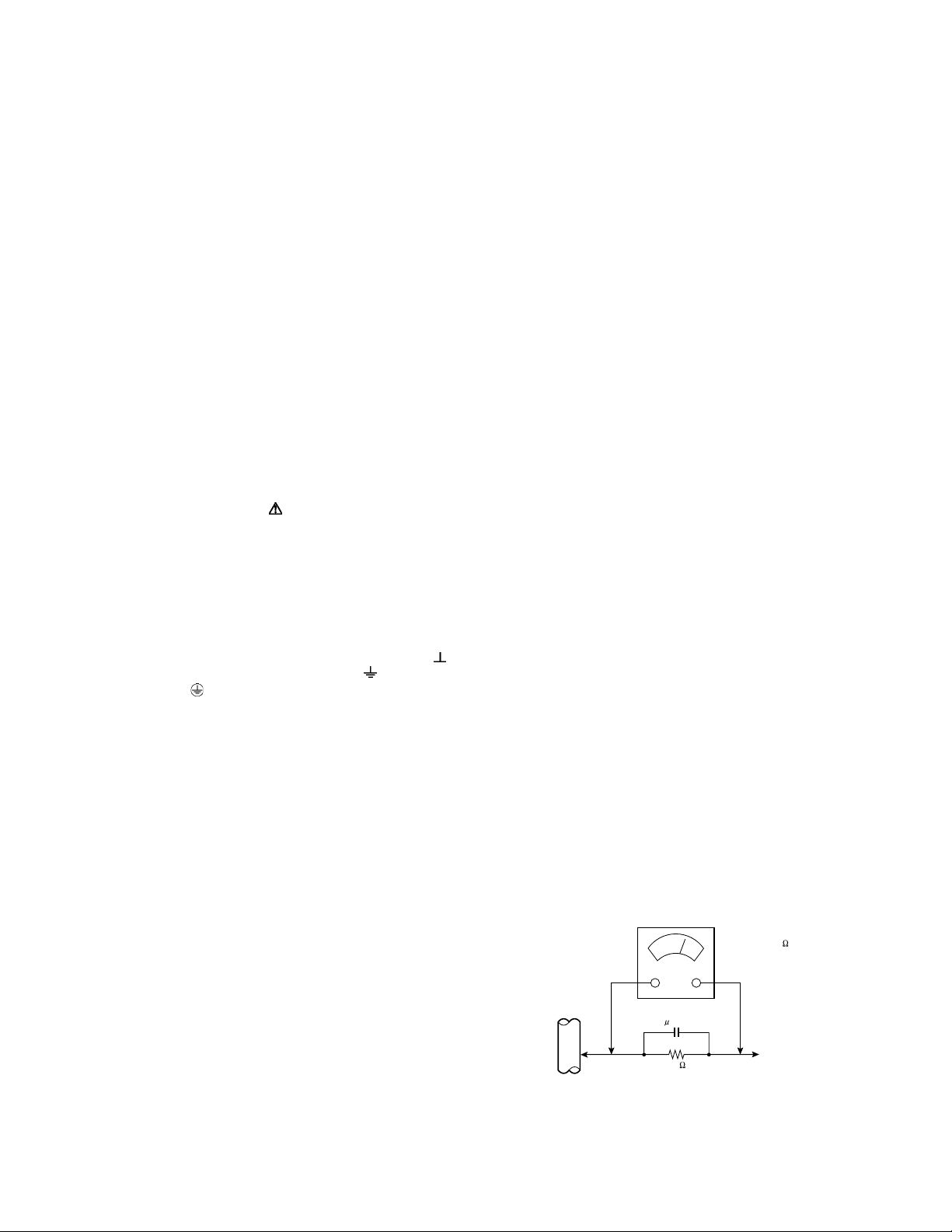
b) Leakage Current Check
Plug the AC line cord directly into the AC outlet (do not use
a line isolation transformer during this check.). Using a
"Leakage Current Tester", measure the leakage current
from each exposed metal part of the cabinet, particularly
any exposed metal part having a return path to the chassis,
to a known good earth ground (water pipe, etc.). Any leakage current must not exceed 0.5mA AC (r.m.s.).
However, in tropical area, this must not exceed 0.2mA AC
(r.m.s.).
Alternate Check Method
Plug the AC line cord directly into the AC outlet (do not
use a line isolation transformer during this check.). Use
an AC voltmeter having 1000Ω per volt or more
sensitivity in the following manner. Connect a 1500Ω
10W resistor paralleled by a 0.15µF AC-type capacitor
between an exposed metal part and a known good earth
ground (water pipe, etc.). Measure the AC voltage
across the resistor with the AC voltmeter. Move the
resistor connection to each exposed metal part,
particularly any exposed metal part having a return path
to the chassis, and measure the AC voltage across the
resistor. Now, reverse the plug in the AC outlet and
repeat each measurement. Any voltage measured must
not exceed 0.75V AC (r.m.s.). This corresponds to
0.7mA AC (r.m.s.).
However, in tropical area, this must not exceed 0.35V
AC (r.m.s.). This corresponds to 0.3mA AC (r.m.s.).
AC VOLTMETER
(HAVING 1000 /V,
OR MORE SENSITIVITY)
0.15 F AC-TYPE
GOOD EARTH GROUND
1500 10W
PLACE THIS PROBE
ON EACH EXPOSED
ME TAL PAR T
(No.YA683<Rev.001>)1-3
Page 4
1.2 SAFETY PRECAUTIONS [FOR UK]
(1) The design of this product contains special hardware and many circuits and components specially for safety purposes. For
continued protection, no changes should be made to the original design unless authorized in writing by the manufacturer.
Replacement parts must be identical to those used in the original circuits. Service should be performed by qualified personnel
only.
(2) Alterations of the design or circuitry of the product should not be made. Any design alterations or additions will void the
manufacturer's warranty and will further relieve the manufacturer of responsibility for personal injury or property damage
resulting therefrom.
(3) Many electrical and mechanical parts in the product have special safety-related characteristics. These characteristics are often
not evident from visual inspection nor can the protection afforded by them necessary be obtained by using replacement
components rated for higher voltage, wattage, etc. Replacement parts which have these special safety characteristics are
identified in the Parts List of Service Manual. Electrical components having such features are identified by shading on the
schematics and by ( ) on the Parts List in the Service Manual. The use of a substitute replacement which does not have the
same safety characteristics as the recommended replacement part shown in the Parts List of Service Manual may cause shock,
fire, or other hazards.
(4) The leads in the products are routed and dressed with ties, clamps, tubing’s, barriers and the like to be separated from live parts,
high temperature parts, moving parts and / or sharp edges for the prevention of electric shock and fire hazard. When service is
required, the original lead routing and dress should be observed, and it should be confirmed that they have been returned to
normal, after re-assembling.
WARNING
(1) The equipment has been designed and manufactured to meet international safety standards.
(2) It is the legal responsibility of the repairer to ensure that these safety standards are maintained.
(3) Repairs must be made in accordance with the relevant safety standards.
(4) It is essential that safety critical components are replaced by approved parts.
(5) If mains voltage selector is provided, check setting for local voltage.
1.3 INSTALLATION
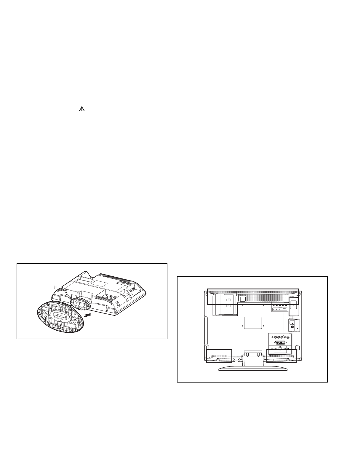
1.3.1 ATTACH THE STAND TO THE TV
When installing the unit on the floor, it is required to attach the
supplied stand.
To attach the stand to the TV, follow the procedure below.
(1) Spread a thick and soft cloth over a table. Place the main
unit face down onto it.
(2) Insert the stand to the main unit slowly.
1.3.2 HEAT DISSIPATION
If the heat dissipation vent behind this unit is blocked, cooling
efficiency may deteriorate and temperature inside the unit will
rise. The temperature sensor that protects the unit will be
activated when internal temperature exceeds the pre-determined
level and power will be turned off automatically.Therefore,
please make sure pay attention not to block the heat dissipation
vent as well as the ventilation outlet behind the unit and ensure
that there is room for ventilation around it.
Ventilation hole
*The drawing may differ from the actual appearance.
1-4 (No.YA683<Rev.001>)
Page 5
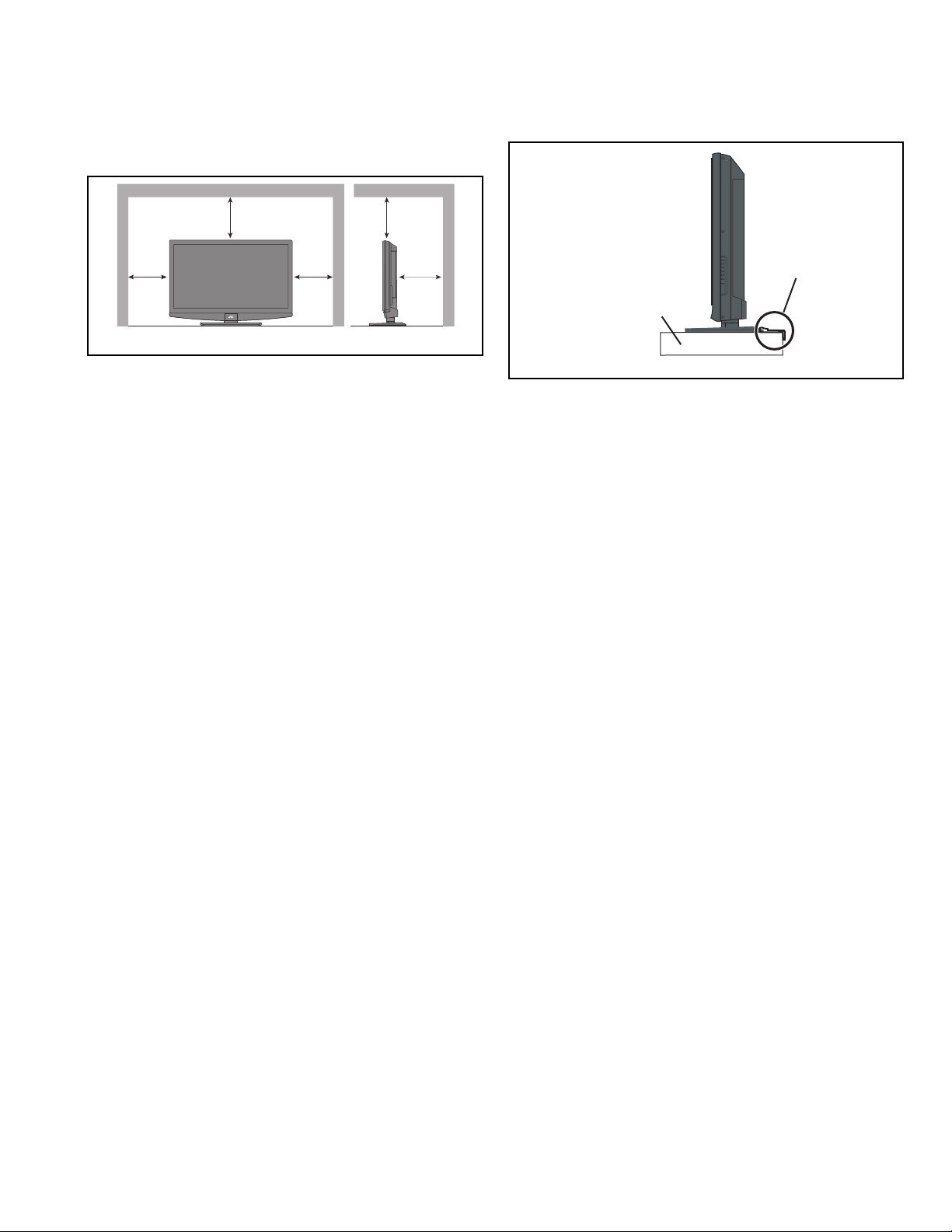
1.3.3 INSTALLATION REQUIREMENTS
Ensure that the minimal distance is maintained, as specified
below, between the unit with and the surrounding walls, as well
as the floor etc.Install the unit on stable flooring or stands.Take
precautionary measures to prevent the unit from tipping in order
to protect against accidents and earthquakes.
1.3.4 INSTALLATION REQUIREMENTS
To ensure safety in an emergency such as an earthquake, and
to prevent accidents, ensure that measures are taken to prevent
the TV dropping or falling over.
200 mm
150 mm
*The drawing may differ from the actual appearance.
150 mm
200 mm
50 mm
1.4 HANDLING LCD PANEL
1.4.1 PRECAUTIONS FOR TRANSPORTATION
When transporting the unit, pressure exerted on the internal LCD
panel due to improper handling (such as tossing and dropping)
may cause damages even when the unit is carefully packed. To
prevent accidents from occurring during transportation, pay
careful attention before delivery, such as through explaining the
handling instructions to transporters.
Ensure that the following requirements are met during
transportation, as the LCD panel of this unit is made of glass and
therefore fragile:
(1) USE A SPECIAL PACKING CASE FOR THE LCD PANEL
When transporting the LCD panel of the unit, use a special
packing case (packing materials). A special packing case
is used when a LCD panel is supplied as a service spare
part.
(2) ATTACH PROTECTION SHEET TO THE FRONT
Since the front (display part) of the panel is vulnerable,
attach the protection sheet to the front of the LCD panel
before transportation. Protection sheet is used when a LCD
panel is supplied as a service spare part.
(3) AVOID VIBRATIONS AND IMPACTS
The unit may be broken if it is toppled sideways even when
properly packed. Continuous vibration may shift the gap of
the panel, and the unit may not be able to display images
properly. Ensure that the unit is carried by at least 2
persons and pay careful attention not to exert any vibration
or impact on it.
(4) DO NOT PLACE EQUIPMENT HORIZONTALLY
Ensure that it is placed upright and not horizontally during
transportation and storage as the LCD panel is very
vulnerable to lateral impacts and may break. During
transportation, ensure that the unit is loaded along the
traveling direction of the vehicle, and avoid stacking them
on one another. For storage, ensure that they are stacked
in 2 layers or less even when placed upright.
It fixes in a band.
TV STAND
*The drawing may differ from the actual appearance.
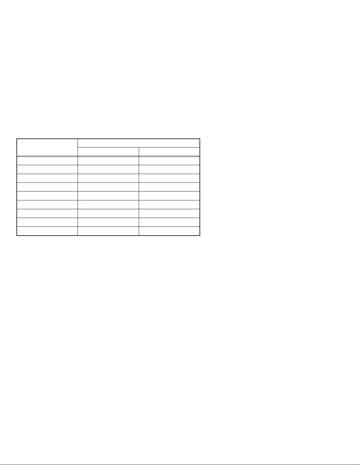
1.3.5 NOTES ON HANDLING
When taking the unit out of a packing case, do not grasp the
upper part of the unit. If you take the unit out while grasping the
upper part, the LCD PANEL may be damaged because of a
pressure. Instead of grasping the upper part, put your hands on
the lower backside or sides of the unit.
1.4.2 OPTICAL FILTER (ON THE FRONT OF THE LCD PANEL)
(1) Avoid placing the unit under direct sunlight over a
prolonged period of time. This may cause the optical filter
to deteriorate in quality and color.
(2) Clean the filter surface by wiping it softly and lightly with a
soft and lightly fuzz cloth (such as outing flannel).
(3) Do not use solvents such as benzene or thinner to wipe the
filter surface. This may cause the filter to deteriorate in
quality or the coating on the surface to come off. When
cleaning the filter, usually use the neutral detergent diluted
with water. When cleaning the dirty filter, use water-diluted
ethanol.
(4) Since the filter surface is fragile, do not scratch or hit it with
hard materials. Be careful enough not to touch the front
surface, especially when taking the unit out of the packing
case or during transportation.
1.4.3 PRECAUTIONS FOR REPLACEMENT OF EXTERIOR
PARTS
Take note of the following when replacing exterior parts (REAR
COVER, FRONT PANEL, etc.):
(1) Do not exert pressure on the front of the LCD panel (filter
surface). It may cause irregular color.
(2) Pay careful attention not to scratch or stain the front of the
LCD panel (filter surface) with hands.
(3) When replacing exterior parts, the front (LCD panel) should
be placed facing downward. Place a mat, etc. underneath
to avoid causing scratches to the front (filter surface).
(No.YA683<Rev.001>)1-5
Page 6
SECTION 2
SPECIFIC SERVICE INSTRUCTIONS
2.1 FEATURES
DIGITAL TUNER
This TV can receive both DVB-T (Digital terrestrial broadcasting),
DVB-S(Digital satellite broadcasting: DB9 only) and Analogue
terrestrial broadcasting.
HDMI INPUT
By connecting a HDMI compatible device, high definition
pictures can be displayed on your TV in their digital form.
2.2 MAIN DIFFERENCE LIST
PICTURE MODE
This function can adjust the picture settings automatically.
There are Standard, Dynamic, Movie and News in the
PICTURE MODE.
ZOOM
This function can change the screen size according to the
picture aspect ratio.
Items
Teletext System (Digital) MHEG 5 UK profile EBU TEXT
POWER CORD UK TYPE (3-pins) EU TYPE (2-pins)
MAIN PWB FU-1ESA19688-1 FU-1ESA19148-1
FUNCTION PWB FU-1ESA19688-2 FU-1ESA19148-2
IR SENSOR PWB FU-1ESA19688-1 FU-1ESA19148-3
JACK PWB FU-1ESA19688-4 FU-1ESA19148-4
INVERTER PWB FU-1ESA19502-1 FU-1ESA19502-1
JUNCTION PWB FU-1ESA19502-2 FU-1ESA19502-2
DIGITAL MAIN UNIT FU-1ESA19709 FU-1ESA19153
LT-19DA9BJ LT-19DA9BU
Contents
1-6 (No.YA683<Rev.001>)
Page 7
2.3 STANDARD NOTES FOR SERVICING
2.3.1 CIRCUIT BOARD INDICATIONS
(1) The output pin of the 3 pin Regulator ICs is indicated as
shown.
Top View
Bottom View
Input
Out
(2) For other ICs, pin 1 and every fifth pin are indicated as
shown.
In
5
Pin 1
10
(3) The 1st pin of every male connector is indicated as shown.
Pin 1
2.3.2 INSTRUCTIONS FOR CONNECTORS
(1) When you connect or disconnect the FFC (Flexible Foil
Connector) cable, be sure to first disconnect the AC cord.
(2) FFC (Flexible Foil Connector) cable should be inserted
parallel into the connector, not at an angle.
FFC Cable
Connector
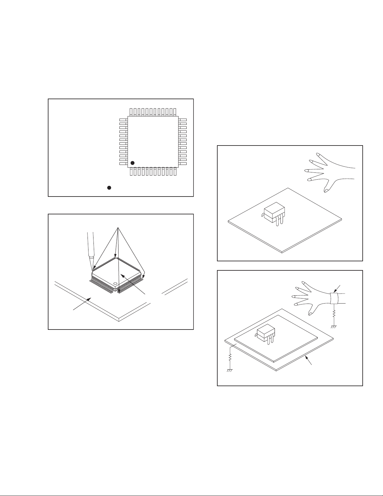
2.3.4 HOW TO REMOVE / INSTALL FLAT PACK-IC
2.3.4.1 REMOVAL
WITH HOT-AIR FLAT PACK-IC DESOLDERING MACHINE:
(1) Prepare the hot-air flat pack-IC desoldering machine,
then apply hot air to the Flat Pack-IC (about 5 to 6
seconds). (Fig.2-1)
Fig.2-1
(2) Remove the flat pack-IC with tweezers while applying
the hot air.
(3) Bottom of the flat pack-IC is fixed with glue to the PWB;
when removing entire flat pack-IC, first apply soldering
iron to center of the flat pack-IC and heat up. Then
remove (glue will be melted). (Fig.2-6)
(4) Release the flat pack-IC from the PWB using tweezers.
(Fig.2-6)
CAUTION:
(1) The Flat Pack-IC shape may differ by models. Use an
appropriate hot-air flat pack-IC desoldering machine,
whose shape matches that of the Flat Pack-IC.
(2) Do not supply hot air to the chip parts around the flat
pack-IC for over 6 seconds because damage to the
chip parts may occur. Put masking tape around the flat
pack-IC to protect other parts from damage. (Fig.2-2)
(3) The flat pack-IC on the PWB is affixed with glue, so be
careful not to break or damage the foil of each pin or
the solder lands under the IC when removing it.
CBA
* Be careful to avoid a short circuit.
2.3.3 PB (LEAD) FREE SOLDER
Pb free mark will be found on PCBs which use Pb free
solder. (Refer to figure.) For PCBs with Pb free mark, be sure
to use Pb free solder. For PCBs without Pb free mark, use
standard solder.
Pb free mark
CBA
Masking
Tape
Tweezers
Hot-air
Flat Pack-IC
Desoldering
Machine
Flat Pack-IC
Fig.2-2
(No.YA683<Rev.001>)1-7
Page 8
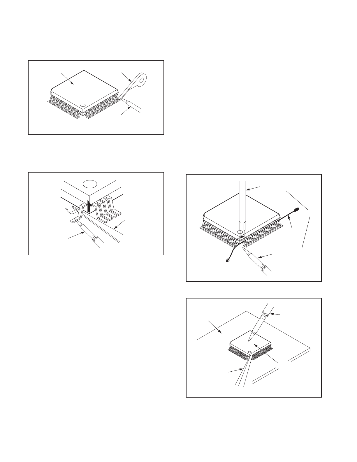
WITH SOLDERING IRON:
(1) Using desoldering braid, remove the solder from all pins
of the flat pack-IC. When you use solder flux which is
applied to all pins of the flat pack-IC, you can remove it
easily. (Fig.2-3)
Flat Pack-IC
Desoldering Braid
Soldering Iron
Fig.2-3
(2) Lift each lead of the flat pack-IC upward one by one,
using a sharp pin or wire to which solder will not adhere
(iron wire). When heating the pins, use a fine tip
soldering iron or a hot air desoldering machine. (Fig.2-4)
WITH IRON WIRE:
(1) Using desoldering braid, remove the solder from all pins
of the flat pack-IC. When you use solder flux which is
applied to all pins of the flat pack-IC, you can remove it
easily. (Fig.2-3)
(2) Affix the wire to a workbench or solid mounting point, as
shown in Fig.2-5.
(3) While heating the pins using a fine tip soldering iron or
hot air blower, pull up the wire as the solder melts so as
to lift the IC leads from the PWB contact pads as shown
in Fig.2-5.
(4) Bottom of the flat pack-IC is fixed with glue to the PWB;
when removing entire flat pack-IC, first apply soldering
iron to center of the flat pack-IC and heat up. Then
remove (glue will be melted). (Fig.2-6)
(5) Release the flat pack-IC from the PWB using tweezers.
(Fig.2-6)
NOTE:
When using a soldering iron, care must be taken to ensure
that the flat pack-IC is not being held by glue. When the flat
pack-IC is removed from the PWB, handle it gently because
it may be damaged if force is applied.
Hot Air Blower
Sharp
Pin
Fine Tip
Soldering Iron
Fig.2-4
(3) Bottom of the flat pack-IC is fixed with glue to the PWB;
when removing entire flat pack-IC, first apply soldering
iron to center of the flat pack-IC and heat up. Then
remove (glue will be melted). (Fig.2-6)
(4) Release the flat pack-IC from the PWB using tweezers.
(Fig.2-6)
To Solid
Mounting Point
CBA
Tweezers
or
Iron Wire
Soldering Iron
Fig.2-5
Fine Tip
Soldering Iron
Flat Pack-IC
1-8 (No.YA683<Rev.001>)
Fig.2-6
Page 9
2.3.4.2 INSTALLATION
(1) Using desoldering braid, remove the solder from the foil of
each pin of the flat pack-IC on the PWB so you can install
a replacement flat pack-IC more easily.
(2) The z mark on the flat pack-IC indicates pin 1. (See Fig.2-
7.) Be sure this mark matches the 1 on the PCB when
positioning for installation. Then presolder the four corners
of the flat pack-IC. (See Fig.2-8.)
(3) Solder all pins of the flat pack-IC. Be sure that none of the
pins have solder bridges.
Example :
Pin 1 of the Flat Pack-IC
is indicated by a " " mark.
Fig.2-7
2.3.5 INSTRUCTIONS FOR HANDLING SEMICONDUCTORS
Electrostatic breakdown of the semi-conductors may occur due
to a potential difference caused by electrostatic charge during
unpacking or repair work.
2.3.5.1 GROUND FOR HUMAN BODY
Be sure to wear a grounding band (1MΩ) that is properly
grounded to remove any static electricity that may be charged on
the body.
2.3.5.2 GROUND FOR WORKBENCH
Be sure to place a conductive sheet or copper plate with proper
grounding (1MΩ) on the workbench or other surface, where the
semi-conductors are to be placed. Because the static electricity
charge on clothing will not escape through the body grounding
band, be careful to avoid contacting semi-conductors with your
clothing.
<I
ncorrec
t
>
CBA
Presolder
Fig.2-8
Flat Pack-IC
<
C
orrec
1M
CBA
t
>
Grounding Band
1M
CBA
Conductive Sheet or
Copper Plate
(No.YA683<Rev.001>)1-9
Page 10
SECTION 3
DISASSEMBLY
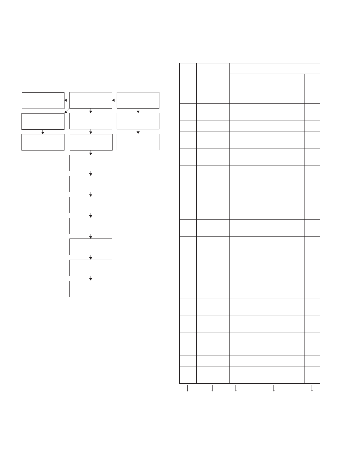
3.1 DISASSEMBLY FLOWCHART
This flowchart indicates the disassembly steps for the cabinet
parts, and the CBA in order to gain access to item(s) to be serviced. When reassembling, follow the steps in reverse order.
Bend, route and dress the cables as they were.
[15] Speaker(s)
[12] IR Sensor PWB
[13] Function PWB
[4] Rear Cabinet
[5] Jack PWB
[6] Shield Box
[1] Stand Cover
[2] Stand Neck
[3] Stand Hinge
Removal
Step/
Loc.
No.
Part
Remove/*Unhook/
Fig.
No.
Unlock/Release/
Unplug/Unclamp/
Desolder
[1]
Stand
Cover
D1 2(S-1) ---
[2] Stand Neck D1 2(S-2) ---
Stand
[3]
Hinge
D1 --------------- ---
Note
[7] Digital Main
Unit
[8] Shield(T)
[9] Main PWB
[10] Junction PWB
[11] Inverter PWB
[14] LCD Module
Assembly
[16] Front Cabinet
3.2 DISASSEMBLY METHOD
Note:
(1) Order of steps in procedure. When reassembling, follow
the steps in reverse order. These numbers are also used
as the Identification (location) No. of parts in figures.
(2) Parts to be removed or installed.
(3) Fig. No. showing procedure of part location
(4) Identification of parts to be removed, unhooked,
unlocked, released, unplugged, unclamped, or
desoldered.
P = Spring, L = Locking Tab, S = Screw, CN = Connector
* = Unhook, Unlock, Release, Unplug, or Desolder
e.g. 2(S-2) = two Screws (S-2), 2(L-2) = two Locking
Tabs (L-2)
(5) Refer to the following "Reference Notes in the Table."
Rear
[4]
Cabinet
[5] Jack PWB
2(S-3), 7(S-4),
D1
*7(L-1)
D2
2(S-5), *CN107 ---
D3
---
2(S-6), (S-7), 5(S-8),
6(S-9), *CN101A,
[6] Shield Box
D2
*CN102A, *CN103A,
D3
*CN104A, *CN4501,
---
*CN4502, FFC Shield
Digital Main
[7]
Unit
D2D32(S-10), Connector IC
Card OSU
---
[8] Shield(T) D2 (S-11a), 2(S-11b) ---
[9] Main PWB
Junction
[10]
PWB
Inverter
[11]
PWB
IR Sensor
[12]
PWB
Function
[13]
PWB
D2D36(S-12), *CN106,
*CN105A, *CN802
D2
*CN403A ---
D3
D2D34(S-13), *CN401,
*CN402, *CN451
D2
*CN301 ---
D3
D2
--------------- ---
D3
---
---
LCD
[14]
Module
D2 --------------- ---
Assembly
[15] Speaker(s) D2 4(S-14) ---
Front
[16]
Cabinet
D2 --------------- ---
(1) (2) (3) (4) (5)
1-10 (No.YA683<Rev.001>)
Page 11
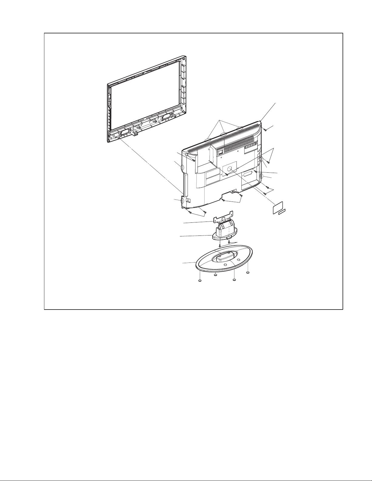
(S-4)
(L-1)
(L-1)
(L-1)
(S-1)
[4] Rear Cabinet
(S-4)
(S-3)
(L-1)
(S-4)
(L-1)
(S-4)
[3] Stand Hinge
[2] Stand Neck
[1] Stand Cover
(S-4)
(S-2)
Fig. D1
(No.YA683<Rev.001>)1-11
Page 12
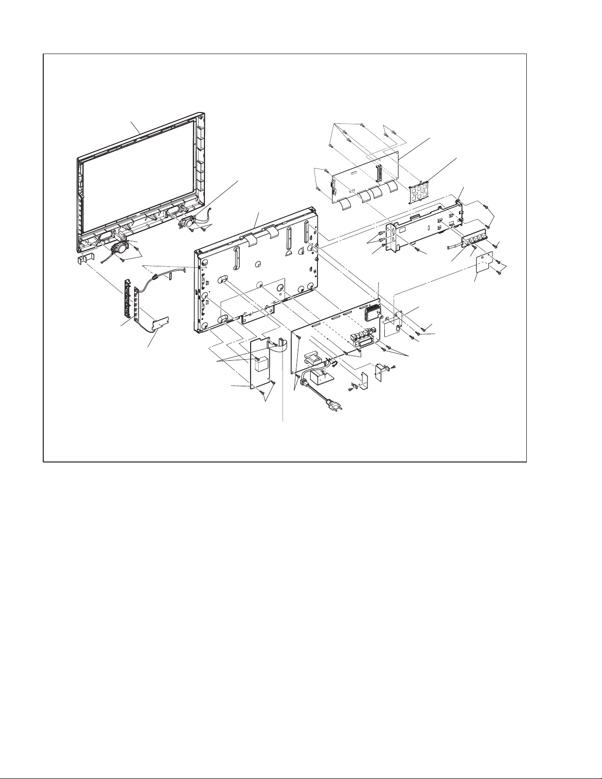
[16] Front Cabinet
[13] Function
PWB
[12] IR Sensor
PWB
[15] Speaker
(S-14)
(S-13)
[15] Speaker
[14] LCD Module
Assembly
(S-14)
(S-9)
(S-9)
(S-10)
(S-6)
(S-7)
[5] Jack PWB
[9] Main PWB
(S-12)
[7] Digital Main
Unit
Connector IC
Card OSU
[6] Shield Box
(S-8)
(S-5)
FFC Shield
[8] Shield(T)
(S-11b)
(S-11a)
(S-11b)
(S-12)
(S-8)
(S-5)
(S-8)
[11] Inverter PWB
(S-12)
(S-13)
[10] Junction PWB
Fig. D2
1-12 (No.YA683<Rev.001>)
Page 13
SECTION 4
ADJUSTMENT
4.1 GENERAL NOTE: “PWB” IS ABBREVIATION FOR
“CIRCUIT BOARD ASSEMBLY.”
NOTE:
Electrical adjustments are required after replacing circuit
components and certain mechanical parts. It is important to
perform these adjustments only after all repairs and
replacements have been completed. Also, do not attempt
these adjustments unless the proper equipment is available.
4.2 TEST EQUIPMENT REQUIRED
(1) Pattern Generator
(2) Color Analyzer
4.3 HOW TO ENTER THE SERVICE MODE
(1) Turn the power on.
(2) While pressing [MUTE] button, press [i] button on the
remote control unit.
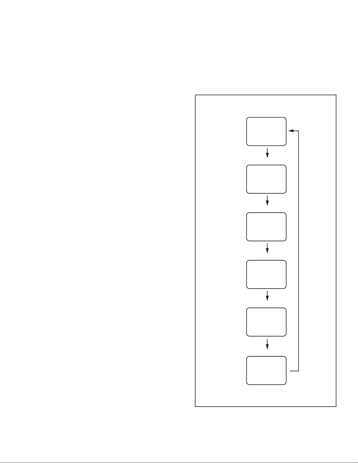
4.4 PURITY CHECK MODE
This mode cycles through full-screen displays of red, green, blue,
and white to check for non-active pixels.
(1) Enter the Service mode.
(2) Each time pressing [7] key on the service remote control
unit, the display changes as follows.
Purity Check Mode
White mode
[7] button
[7] button
Black mode
[7] button
Red mode
[7] button
Green mode
[7] button
Blue mode
[7] button
White 25% mode
Note:
When entering this mode, the default setting is White mode.
(No.YA683<Rev.001>)1-13
Page 14
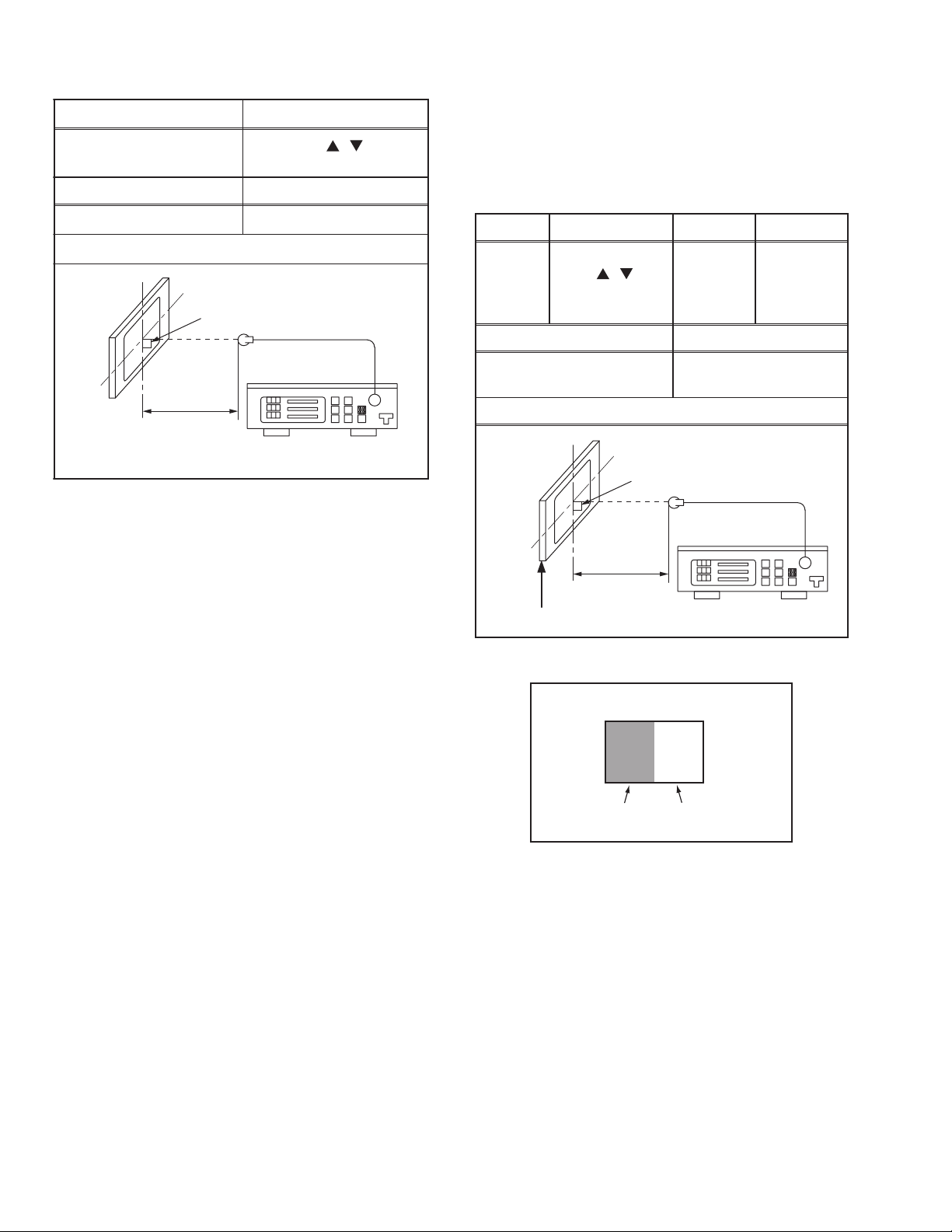
4.5 VCOM ADJUSTMENT.
Test Point
Screen
M. EQ. Spec.
Color analyzer
It carries out in a darkroom.
Perpendicularity
Figure
Adj. Point
[P ]
/
buttons
See below
4.6 WHITE BALANCE ADJUSTMENT
The following adjustment normally are not attempted in the field.
Only when replacing the LCD Panel then adjust as a preparation.
PURPOSE:
To mix red, green and blue beams correctly for pure white.
SYMPTOM OF MISADJUSTMENT:
White becomes bluish or reddish.
Test Point
Adj. Point Mode Input
White Raster
Screen
[P ]
/
buttons
[VIDEO]
C/D
(APL 70%)
or
(APL 30%)
M. EQ. Spec.
L = 3 cm
Color Analyzer
(1) Operate the unit for more than 20 minutes.
(2) Set the color analyzer and bring the optical receptor to the
center on the LCD-Panel surface after zero point calibration as shown above.
NOTE:
The optical receptor must be set perpendicularly to the
LCD Panel surface.
(3) Enter the Service mode.
(4) [VCOM1]
Press [2] key on the service remote control unit.
[VCOM2]
Press [3] key on the service remote control unit.
(5) Press [P / ] bkey on the service remote control unit so
that the color analyzer value becomes minimum.
Pattern Generator,
Color analyzer
x= 0.272 ± 0.005
y= 0.278 ± 0.005
Figure
It carries out in a darkroom.
Perpendicularity
L = 3 cm
INPUT: WHITE 70%, 30%
(1) Operate the unit for more than 20 minutes.
(2) Input the White Raster(70%=70IRE, 25%=25IRE).
INPUT SIGNAL
30%=30IRE
Color Analyzer
70%=70IRE
1-14 (No.YA683<Rev.001>)
(3) Set the color analyzer to the CHROMA mode and bring the
optical receptor to the center on the LCD-Panel surface after zero point calibration as shown above.
NOTE:
The optical receptor must be set perpendicularly to the
LCD Panel surface.
(4) Enter the Service mode. Press [VOLUME -] button on the
service remote control unit and select “C/D” mode.
(5) [CUTOFF]
Press [3] key to select “COB” for Blue Cutoff adjustment.
Press [1] key to select “COR” for Red Cutoff adjustment.
[DRIVE]
Press [6] key to select “DB” for Blue Drive adjustment.
Press [4] key to select “DR” for Red Drive adjustment.
(6) In each color mode, press [P / ] buttons to adjust the
values of color.
(7) Adjust Cutoff and Drive so that the color temperature be-
comes 12000°K (x= 0.272 / y= 0.278 ±0.005).
Page 15
4.7 HOW TO VERIFY THE PROTECT MODE
The Sub CPU always surveys the power supply circuit. If the abnormal voltage is detected on the power supply circuit, a voltage
is not supplied.
Perform the following procedures for confirmation.
(1) Enter the service mode.
The following screen appears.
(2)
"*" differs depending on the models.
Code :
Boot :
System :
SubCPU :
Pic Code :
Picture :
Panel :
Other :
Safety :
HDMI1 Block0 :
Block1 :
HDMI2 Block1 :
**********-***
**** * ***
**** * ***
****
**-***-**-****-***
****
***
**
Safety_Non
**
**
**
SPAIN
Display protection mode
Indication of Safety
INDICATION DESCRIPTION
Safety_Non The power supply circuit is normal.
Safety1 The power supply circuit is abnormal.
(Protect1)
Safety2 The reduced voltage detection circuit is
abnormal. (Protect2)
Safety3 The inverter circuit is abnormal. (Protect3)
4.8 HOW TO INITIALIZE THE LCD TELEVISION
(1) Turn the power on.
(2) To enter the service mode.
• To cancel the service mode, press [POWER] key on the
remote control unit.
(3) Press [AV] key on the service remote control unit to initial-
ize the LCD television.
(4) "INITIALIZED" will appear in the upper right of the screen.
"INITIALIZED" color will change to green from red when
initializing is complete.
(No.YA683<Rev.001>)1-15
Page 16
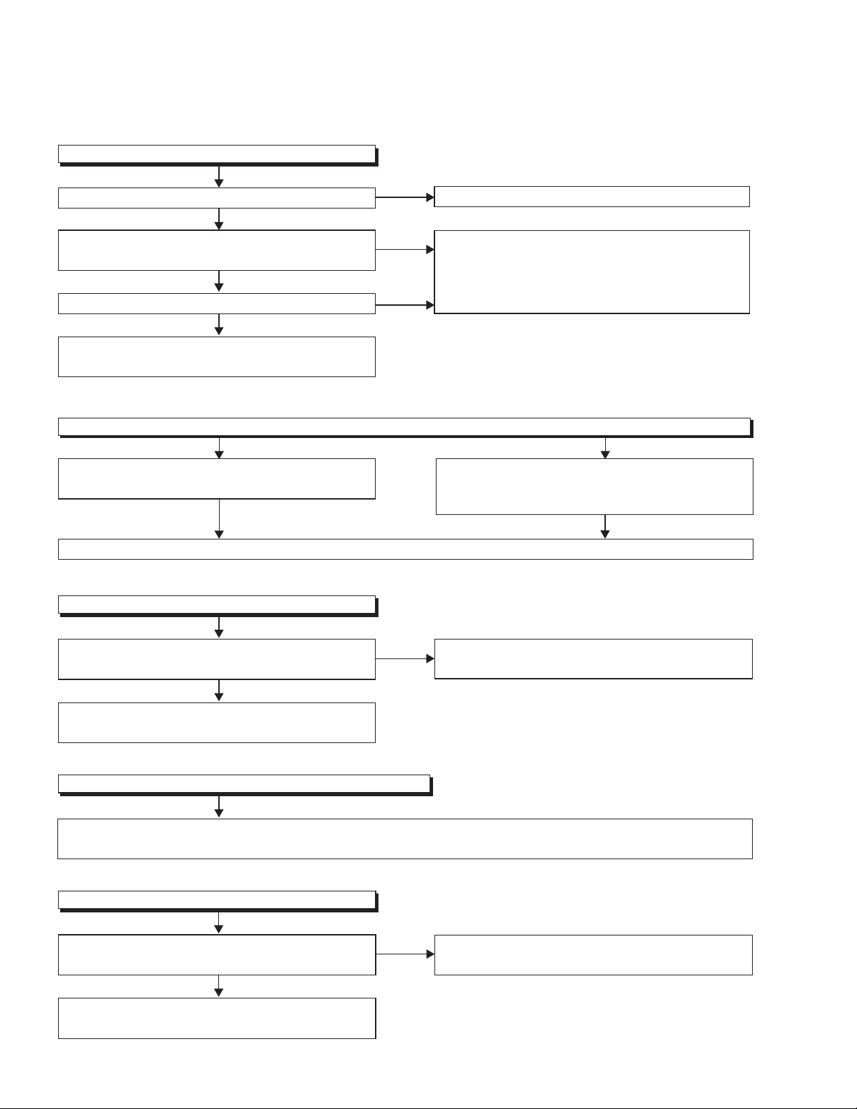
FLOW CHART NO.1
The power cannot be turned on.
SECTION 5
TROUBLESHOOTING
Is the fuse (F601) normal?
Ye s
Is normal state restored when once unplugged power
cord is plugged again several seconds?
Ye s
Is the AL +12V line voltage normal?
Ye s
Check each rectifying circuit of the secondar
and service it if defective.
FLOW CHART NO.2
The fuse blows out.
Check the prese
leaking or shorted and service it if defective.
After ser
FLOW CHART NO.3
When the output voltage fluctuates.
vicing, replace the fus
nce that the primary component is
e (F601).
y circuit
No
No
No
See FLOW CHART No.2 <The fuse blows out.>
Check if there is any leak or short-circuiting on the
primary circuit component, and service it if defective.
(IC601, Q600, Q601, D611, D613, D614, D616,
T601, R610)
Check the prese
is shorted in each rectifying circuit of secondary side,
and service it if de
nce that the rectifying diode or circuit
fective.
Does the photocoupler circuit on the secondar
operate normally?
Ye s
Check IC601, D610, D615 and their pe
service it if defective.
FLOW CHART NO.4
When buzz sound can be heard in the vicinity of power circuit.
Check if there is any short-circuit on the rec
service it if defective. (IC900, IC902, D900, D903, D904, D905, D906, D924, D990, Q901, Q902, Q906, Q908, Q911, Q922, Q936)
FLOW CHART NO.5
+35V is not output.
Is appro
of D903?
Check if there is any leak or short-circuit on the loaded
circuit, and service it if defective.
ximately 35V voltage supplied to the cathode
Ye s
y side
riphery, and
tifying diode and the circuit in each rectifying circuit of the secondary side, and
No
No
Check IC601, Q900, D913 and their periphery, and
service it if defective.
Check D903, D908, C903 and their periphery circuit,
and service it defective.
1-16 (No.YA683<Rev.001>)
Page 17
FLOW CHART NO.6
INV+22V is not output.
Is approximately 22V voltage supplied to the cathode
of D990?
Ye s
Check if there is any leak or short-circuit on the loaded
circuit, and service it if defective.
FLOW CHART NO.7
AL+3.3V is not output.
Is approximately 8V voltage supplied to the cathode
of D924?
Ye s
Check Q901, D916 and their periphery circuit, and
service it if defective.
FLOW CHART NO.8
P-ON+5V is not output.
Is appro
ximately 8V voltage supplied to the collector
of Q936?
Ye s
Is approximately 6V voltage supplied to the base of
Q936?
Ye s
No
No
No
No
Check D990, C902 and their periphery circuit, and
service it defective.
Check D924, C917 and their periphery circuit, and
service it if defective.
See FLO
W CHART No.7
See FLOW CHART No.9
Replace Q936.
FLOW CHART NO.9
LCD+24.5V is not output.
Is approximately 38V voltage supplied to the cathode
of D903?
Ye s
Is approximately 38V voltage supplied to the collector
of Q911?
No
Is the voltage of base on Q911 lower than the voltage
of emitter on Q911 when turning the power on?
Ye s
Replace Q911.
No
Ye s
No
Check D903, D908, C903 and their periphery circuit,
and service it if de
Check D923 and
fective.
their periphery circuit, and service it
if defective.
Check Q912 and
P-ON-H1 line, and service it if
defective.
(No.YA683<Rev.001>)1-17
Page 18
FLOW CHART NO.10
LCD+13V is not output.
Is approximately 23V voltage supplied to the cathode
of D990?
Ye s
Is approximately 18V voltage supplied to the collector
of Q922?
Ye s
Is approximately 13V voltage supplied to the base of Q922?
Ye s
Replace Q922.
FLOW CHART NO.11
LCD-6.8V is not output.
Is approximately
-12V voltage supp
lied to the anode of
D905?
Ye s
Is approximately -
11V voltage supplied to the base of
Q908?
Ye s
Replace Q908.
No
No
No
No
No
Check D990, C902 and their periphery circuit, and
service it if defective.
Check R953, R954, R955 and their periphery circuit,
and service it if def
ective.
See FLOW CHART No.9
Check D905, C
vice it if defective.
ser
905 and their periphery circuit, and
Check R945 and their periphery circuit, and service it
if defective.
FLOW CHART NO.12
LCD+3.3V is not output.
Is approximately 8V v
oltage supplied to the cathode of
D924?
Is approximately 7
V voltage supplied to the collector
of Q902?
Is approximately 4V voltage suppli
Replace Q902.
Ye s
Ye s
ed to the base of Q902?
Ye s
No
No
No
Check D924, C917 and their periphery circuit, and
vice it if defective.
ser
Check D974, D975 and their periphery circuit, and
service it if defective.
Check D920, R930 and their periphery circuit, and
service it if defective.
1-18 (No.YA683<Rev.001>)
Page 19
FLOW CHART NO.13
+3.5V is not output.
Is approximately 3.5V voltage supplied to the cathode
of D906?
Ye s
Check if there is any leak or short-circuit on the
loaded circuit, and service it if defective.
FLOW CHART NO.14
P-ON+3.3V is not output.
Is approximately 5V voltage supp
lied to the Pi
n(1) of
IC902?
Ye s
Replace IC902.
FLOW CHART NO.15
P-ON+9V is not output.
Is approximately 14V voltage supplied to the
collector of Q906?
Ye s
Is approximately 10V voltage supplied to the
base of Q906?
Ye s
Replace Q906.
No
No
No
No
Check D906, C907 and their periphery circuit, and
service it if defective.
Check D900, C900 and their periphery circuit, and
service it if defective.
r
Check D904, C904 and their pe
iphery circuit, and
service it if defective.
See FLO
W CHART No.9
FLOW CHART NO.16
The key operation is not functioning.
Are the contact point and installation
state of the key
switches (SW201, SW202, SW203, SW204,
SW205, SW206, SW207) normal?
Ye s
When pre
SW203, SW
voltage of P
ssing each switches (SW201, S
204, SW205, SW20
in(1) on CN
104A increase?
6, SW207) do the
Ye s
Replace Digital Main PWB Unit.
W202,
No
No
Re-install the switches (SW201, SW202, SW203,
SW204, SW205, SW206, SW207) correctly or
replace the poor switch.
Check the switches (SW201, SW202, SW203,
SW204, SW205, SW206, SW207) and their
periphery, and service it if defective.
(No.YA683<Rev.001>)1-19
Page 20

FLOW CHART NO.17
No operation is possible from the remote control unit.
Operation is possible from the unit.
Is 3.3V voltage supplied to Pin(2) of RS301 (remote
control receiver)?
No
Check AL+3.3V line and service it if defective.
Ye s
Is the "L" pulse sent out Pin(1) of RS301 (remote control
receiver) when the infrared remote control is activated?
No
Replace the RS301 (remote control receiver) or
remote control unit.
Ye s
Is the "L" pulse supplied to the P
Ye s
in(4) of CN104A?
No
Check the line between Pin(1) of RS301 (remote
control receiver) and Pin(4) of CN104A, and service
it if defective.
Replace Digital Main PWB Unit.
FLOW CHART NO.18
Picture does not appear normally. (Video input/S-Video input/Y/Pb/Pr input/RGB input)
Are the video signals outputted to the specific
terminal?
Are the luminance signals outputted to the Pin(23) of
CN101A?
Are the chrominance signals outputted to the Pin(25)
of CN101A?
Are the component video(Y/Pb/Pr) signals outputted
to the Pin(18, 20, 21) of CN101A?
Are the RGB video signals outputted to the Pin(3, 4, 5)
of CN102A?
Are the composite video signals outputted to the Pin(1)
No
No
No
No
No
Check the line between each pin of CN101A and
CN102A and input terminal and service it if defective.
Check the luminance signal line, and service it if
defective.
Check the chrominance signal line, and service it if
defective.
Check the component video(Y/Pb/Pr) signal line,
and service it if defective.
Check the RGB video signal line, and service it if
defective.
of CN102A?
Ye s
Replace Digital Main PWB Unit or LCD Module
Assembly.
Ye s
(RCA JACK input)
Are the composite video signals inputted to the Pin(2)
of IC851?
(SCART JACK input)
Are the composite video signals inputted to the Pin(1)
of IC851?
Ye s
Are the composite video signals outputted to the
Pin(15) of IC851?
Ye s
Check the line between Pin(15) of IC851 and Pin(1) of
CN102A, and service it if defective.
1-20 (No.YA683<Rev.001>)
No
No
No
Check the line between Pin(2) of IC851 and JK722,
and service it if defective.
Check the line between Pin(1) of IC851 and JK751,
and service it if defective.
Is approximately 9V voltage supplied to the Pin(16) of
IC851?
Ye s
No
Replace IC851. Check P-ON+9V line,
and service it if defective.
Page 21

FLOW CHART NO.19
Picture does not appear normally.
Are the DIF signals outputted to the Pin(20, 22) of CN103A?
Ye s
Replace Digital Main PWB Unit or LCD Module
Assembly.
FLOW CHART NO.20
Audio is not outputted normally. (Tuner input (Digital))
Are the DIF signals outputted to the Pin(20, 22) of
No
CN103A?
Ye s
Are the audio data signal outputted to the Pin(13) of
No
CN101A?
Ye s
Are the audio(L/R) signals outputted to the Pin(14,15)
No
of IC802?
Ye s
Are the audio(L/R) signals outputted to the Pin(11,14)
No
of IC801?
Ye s
No
Check the line between Pin(20, 22) of CN103A and
Pin(16, 17) of TU501, and TU501(Tuner Unit),
and service it if defective.
Check the line between Pin(20, 22) of CN103A and
Pin(16, 17) of TU501, and TU501(Tuner Unit), and
service it if defective.
Replace Digital Main Unit.
Check IC802 and the periphery circuit, and service it
if defective.
Check IC801 and the periphery circuit, and service it
if defective.
Check SP451,SP802, JK801 and their periphery
circuit, and service it if defective.
FLOW CHART NO.21
Audio is not outputted normally. (Audio input terminals)
Are the audio (L/R) signals outputted to the
Pin(3, 4) of CN103A?
Ye s
Are the audio data signal outputted to the Pin(13) of
CN101A?
Ye s
Are the audio(L/R) signals outputted to the Pin(14,15)
of IC802?
Ye s
Are the audio(L/R) signals outputted to the Pin(11,14)
of IC801?
Ye s
Check SP451,SP802, JK801 and their periphery
circuit, and service it if defective.
No
No
No
No
Check the line between Pin(3, 4) of CN103A and
each Audio input terminal(JK14, JK15, JK723, JK724,
JK725, JK751) and IC850, and service it if defective.
Replace Digital Main PWB Unit.
Check IC802 and the periphery circuit, and service
it if defective.
Check IC801 and the periphery circuit, and service
it if defective.
(No.YA683<Rev.001>)1-21
Page 22

Victor Company of Japan, Limited
Display Division 12, 3-chome, Moriya-cho, Kanagawa-ku, Yokohama-city, Kanagawa-prefecture, 221-8528, Japan
(No.YA683<Rev.001>)
Printed in Japan
VPT
Page 23

PARTS LIST
CAUTION
J The parts identified by the symbol are important for the safety . Whenever replacing these parts, be sure to use specified ones to secure the
safety.
J The parts not indicated in this Parts List and those which are filled with lines --- in the Parts No. columns will not be supplied.
J P.W. BOARD Ass'y will not be supplied, but those which are filled with the Parts No. in the Parts No. columns will be supplied.
ABBREVIATIONS OF RESISTORS, CAPACITORS AND TOLERANCES
RESISTORS CAPACITORS
CR Carbon Resistor C CAP. Ceramic Capacitor
FR Fusible Resistor E CAP. Electrolytic Capacitor
PR Plate Resistor M CAP. Mylar Capacitor
VR Variable Resistor CH CAP. Chip Capacitor
HV R High Voltage Resistor HV CAP. High Voltage Capacitor
MF R Metal Film Resistor MF CAP. Metalized Film Capacitor
MG R Metal Glazed Resistor MM CAP. Metalized Mylar Capacitor
MP R Metal Plate Resistor MP CAP. Metalized Polystyrol Capacitor
OM R Metal Oxide Film Resistor PP CAP. Polypropylene Capacitor
CMF R Coating Metal Film Resistor PS CAP. Polystyrol Capacitor
UNF R Non-Flammable Resistor TF CAP. Thin Film Capacitor
CH V R Chip Variable Resistor MPP CAP. Metalized Polypropylene Capacitor
CH MG R Chip Metal Glazed Resistor TAN. CAP. Tantalum Capacitor
COMP. R Composition Resistor CH C CAP. Chip Ceramic Capacitor
LPTC R Linear Positive Temperature Coefficient Resistor BP E CAP. Bi-Polar Electrolytic Capacitor
CH AL E CAP. Chip Aluminum Electrolytic Capacitor
CH AL BP CAP. Chip Aluminum Bi-Polar Capacitor
CH TAN. E CAP. Chip Tantalum Electrolytic Capacitor
CH AL BP E CAP. Chip Tantalum Bi-Polar Electrolytic Capacitor
RESISTORS
FGJ KMNRHZP
±1% ±2% ±5% ±10% ±20% ±30%
+30%
-10%
+50%
-10%
+80%
-20%
+100%
-0%
(No.YA683<Rev.001>)3-1
Page 24

CONTENTS
USING P.W. BOARD ................................................................................................................................................... 3-2
EXPLODED VIEW PARTS LIST ................................................................................................................................. 3-3
EXPLODED VIEW ....................................................................................................................................................... 3-4
PRINTED WIRING BOARD PARTS LIST [LT-19DA1BJ/AK] .................................................................................... 3-6
MAIN P.W. BOARD ASS'Y (FU-1ESA19688-1) ................................................................................................ 3-6
FUNCTION P.W. BOARD ASS'Y (FU-1ESA19688-2) ....................................................................................... 3-8
IR SENSOR P.W. BOARD ASS'Y (FU-1ESA19688-3) ...................................................................................... 3-8
JACK P.W. BOARD ASS'Y (FU-1ESA19688-4) ................................................................................................ 3-8
INVERTER P.W. BOARD ASS'Y (FU-1ESA19502-1) ....................................................................................... 3-9
JUNCTION P.W. BOARD ASS'Y (FU-1ESA19502-2) ....................................................................................... 3-9
PRINTED WIRING BOARD PARTS LIST [LT-19DA1BU/AK] ................................................................................. 3-10
MAIN P.W. BOARD ASS'Y (FU-1ESA19148-1) .............................................................................................. 3-10
FUNCTION P.W. BOARD ASS'Y (FU-1ESA19148-2) .....................................................................................3-12
IR SENSOR P.W. BOARD ASS'Y (FU-1ESA19148-3) ....................................................................................3-12
JACK P.W. BOARD ASS'Y (FU-1ESA19148-4) .............................................................................................. 3-12
INVERTER P.W. BOARD ASS'Y (FU-1ESA19502-1) .....................................................................................3-13
JUNCTION P.W. BOARD ASS'Y (FU-1ESA19502-2) .....................................................................................3-13
PACKING ................................................................................................................................................................... 3-14
PACKING PARTS LIST ............................................................................................................................................. 3-15
USING P.W. BOARD
P.W.B ASS'Y name
LT-19DA1BJ/AK LT-19DA1BU/AK
MAIN P.W.B FU-1ESA19688-1 FU-1ESA19148-1
FUNCTION P.W.B FU-1ESA19688-2 FU-1ESA19148-2
IR SENSOR P.W.B FU-1ESA19688-3 FU-1ESA19148-3
JACK P.W.B FU-1ESA19688-4 FU-1ESA19148-4
INVERTER P.W.B FU-1ESA19502-1
JUNCTION P.W.B FU-1ESA19502-2
DIGITAL MAIN P.W.B FU-1ESA19709 FU-1ESA19153
P.W.B ASS'Y No.
←
←
3-2(No.YA683<Rev.001>)
Page 25

EXPLODED VIEW PARTS LIST
Ref.No. Part No. Part Name Description Local
1 FU-1EM023085 REAR CABINET
2 FU-1EM023353 FRONT CABINET
3 FU-UG190EB LCD PANEL UNIT
4 FU-1EM222223A DECORATION PLATE
5 FU-DSD0806XQ001 SPEAKER
6 FU-DSD0806XQ001 SPEAKER
7 FU-WAB0182K5002 POWER CORD LT-19DA1BJAK
7 FU-WAE0172LW006 POWER CORD LT-19DA1BUAK
10 FU-1EM427137 REAR COVER
11 FU-1EM323959 SENSOR LED LENS
12 FU-1EM426377 STAND RUBBER FOOT (x4)
13 FU-1EM022467 STAND COVER
16 FU-1EM325277 STAND NECK
22 FU-1EM222143A FUNCTION KNOB
25 FU-1EM323797 WALL MOUNT BRACKET (x4)
26 FU-1EM122473 SHIELD BOX
27 FU-1EM325219 SHIELD (T)
28 FU-1EM427320 FFC SHIELD
29 FU-1EM323940 STAND HINGE
30 FU-0EM404486 CLOTH
31 FU-1EM424258 CLOTH
32 FU-1EM425861 GASKET (x2)
33 FU-0EM400076 CLOTH(B) (x4)
35 FU-GBJS3060 SCREW M3x6(x25)
36 FU-0EM408146A DOUBLE SEMS SCREW M4x9(x2)
37 FU-1EM422042 HEX SCREW (x2)
38 FU-FPJ32100 DOUBLE SEMS SCREW M2x10(x2)
39 FU-GBJP3100 SCREW M3x10(x8)
40 FU-FPJ32060 DOUBLE SEMS SCREW M2x6(x2)
41 FU-GBHP3100 SCREW M3x10(x7)
42 FU-GBHP4180 SCREW M4x18(x2)
43 FU-GBHS3060 SCREW M3x6(x2)
44 FU-GBHS3040 SCREW M3x4(x2)
50 FU-WX1A8CN0-012 WIRE ASSEMBLY 7pin CL107
51 FU-WX1A8CN0-013 WIRE ASSEMBLY 2pin CL451
52 FU-WX1A8CN0-013 WIRE ASSEMBLY 2pin CL802
53 FU-WX1A8CN0-006 WIRE ASSEMBLY 25pin CL3601
54 FU-WX1A8CN0-006 WIRE ASSEMBLY 25pin CL3701
55 FU-WX1A8CN0-005 WIRE ASSEMBLY 23pin CL3704
56 FU-WX1A8A70-101 FFC WIRE 55pin CL4501
57 FU-WX1A8A70-101 FFC WIRE 55pin CL4502
58 FU-WX1A8CN0-006 WIRE ASSEMBLY 25pin CL4503
59 FU-J6Q568CTK002 IC CARD CONNECTOR
101 FU-1ESA19688-1 MAIN PWB Please note that the TUNER is not included in MAIN PWB LT-19DA1BJAK
101 FU-1ESA19148-1 MAIN PWB Please note that the TUNER is not included in MAIN PWB LT-19DA1BUAK
102 FU-1ESA19688-2 FUNCTION PWB LT-19DA1BJAK
102 FU-1ESA19148-2 FUNCTION PWB LT-19DA1BUAK
103 FU-1ESA19688-3 IR SENSOR PWB LT-19DA1BJAK
103 FU-1ESA19148-3 IR SENSOR PWB LT-19DA1BUAK
104 FU-1ESA19688-4 JACK PWB LT-19DA1BJAK
104 FU-1ESA19148-4 JACK PWB LT-19DA1BUAK
105 FU-1ESA19502-1 INVERTER PWB
106 FU-1ESA19502-2 JUNCTION PWB
107 FU-1ESA19709 DIGITAL MAIN PWB LT-19DA1BJAK
107 FU-1ESA19153 DIGITAL MAIN PWB LT-19DA1BUAK
TU1 FU-UTUNPSGAL013 TUNER UNIT TU501
(No.YA683<Rev.001>)3-3
Page 26

EXPLODED VIEW
5
22
3333
44
3333
3333
5252
5656
5757
3535
3838
3535
33
3232
5454
5353
1111
3333
2222
5151
66
102102
3939
103103
55
3939
101101
3535
3535
3535
105105
3535
3535
106106
77
3737
353
3-4(No.YA683<Rev.001>)
Page 27

4040
5858
5555
107107
5959
3535
3939
2525
11
3535
2525
3939
4141
2525
4141
1010
4343
77
3535
2626
5050
3535
3535
104104
2828
TU1TU1
2727
4444
3030
3535
4141
4040
3535
4242
2929
SERIAL
4141
1616
NO.LABEL
RATING LABEL
1313
3636
1212
3636
3131
(No.YA683<Rev.001>)3-5
Page 28

PRINTED WIRING BOARD PARTS LIST [LT-19DA1BJ/AK]
MAIN P.W. BOARD ASS'Y (FU-1ESA19688-1)
Ref No. Part No. Part Name Description Local
IC601 FU-QPEL561L11AV PHOTO COUPLER
IC801 FU-QSZBA0SMS017 IC
IC802 FU-NSZBA0TTY192 IC AUDIO D/A
IC850 FU-QSZBA0TTS162 IC SWITCHING
IC851 FU-QSZBA0TTS163 IC SWITCH
IC900 FU-NSZBA0SJY041 IC REG 5V
IC902 FU-NSZBA0SJY062 IC REG
Q505 FU-NQS4KTC3199P TRANSISTOR
Q600 FU-QFWZ02SK3566 FET
Q601 FU-QQS02SC2120F TRANSISTOR
Q726 FU-NQS1KTA1267P TRANSISTOR
Q727 FU-NQS1KTA1267P TRANSISTOR
Q731 FU-NQS4KTC3199P TRANSISTOR
Q734 FU-NQS1KTA1267P TRANSISTOR
Q744 FU-NQS4KTC3199P TRANSISTOR
Q802 FU-NQS4KTC3199P TRANSISTOR
Q805 FU-NQS4KTC3199P TRANSISTOR
Q900 FU-NQS4KTC3199P TRANSISTOR
Q901 FU-QQS02SC2120F TRANSISTOR
Q902 FU-QQS02SC2120F TRANSISTOR
Q903 FU-NQS4KTC3199P TRANSISTOR
Q904 FU-NQS4KTC3199P TRANSISTOR
Q906 FU-QQS02SC2120F TRANSISTOR
Q907 FU-NQS1KTA1267P TRANSISTOR
Q908 FU-NQS4KTC3199P TRANSISTOR
Q911 FU-NQS1KTA1267P TRANSISTOR
Q912 FU-NQS4KTC3199P TRANSISTOR
Q920 FU-NQS4KTC3199P TRANSISTOR
Q922 FU-NQE0KTD2059P TRANSISTOR
Q936 FU-QQWZ2SC4881F POW TRANSISTOR
D501 FU-QDTZ001SS133 SI DIODE
D610 FU-QDTB00MTZJ22 ZENER DIODE
D611 FU-NDLZ001N5399 SI DIODE
D612 FU-QDTB0MTZJ5R6 ZENER DIODE
D613 FU-NDLZ001N5399 SI DIODE
D614 FU-NDLZ001N5399 SI DIODE
D615 FU-QDTZ001SS133 SI DIODE
D616 FU-NDLZ001N5399 SI DIODE
D621 FU-QDTZ001SS133 SI DIODE
D622 FU-QDTZ001SS133 SI DIODE
D624 FU-QDLZ001ZC18Q ZENER DIODE
D629 FU-QDTB00MTZJ33 ZENER DIODE
D701 FU-QDTB00MTZJ13 ZENER DIODE
D702 FU-QDTB00MTZJ13 ZENER DIODE
D755 FU-QDTB0MTZJ3R9 ZENER DIODE
D758 FU-QDTB00MTZJ13 ZENER DIODE
D802 FU-QDTZ001SS133 SI DIODE
D803 FU-QDTB0MTZJ4R7 ZENER DIODE
D900 FU-NDQZ000SB360 SB DIODE
D901 FU-NDL1000FR104 FR DIODE
D903 FU-NDL1000FR104 FR DIODE
D904 FU-NDLZ000FR154 DIODE
D905 FU-NDL1000FR104 FR DIODE
D906 FU-NDQZ000SB340 SB DIODE
D908 FU-QDLZ001ZC43Q DIODE
D909 FU-NDQZ001N4005 SI DIODE
D910 FU-QDTZ001SS133 SI DIODE
D911 FU-QDTZ001SS133 SI DIODE
D912 FU-QDTZ001SS133 SI DIODE
D913 FU-QDTB0MTZJ5R6 ZENER DIODE
D915 FU-QDTB00MTZJ33 ZENER DIODE
D916 FU-NSZBA0TJY036 IC REGULATOR
D918 FU-QDTB00MTZJ12 ZENER DIODE
D919 FU-QDTZ001SS133 SI DIODE
D920 FU-NSZBA0TJY036 IC REGULATOR
D922 FU-QDTZ001SS133 SI DIODE
D923 FU-QDTB00MTZJ24 ZENER DIODE
D924 FU-NDWZ000SB270 SB DIODE
D925 FU-QDTZ001SS133 SI DIODE
D926 FU-QDTB00MTZJ10 ZENER DIODE
D927 FU-QDTZ001SS133 SI DIODE
D928 FU-QDTB0MTZJ6R8 ZENER DIODE
D929 FU-QDTZ001SS133 SI DIODE
D930 FU-QDTZ001SS133 SI DIODE
D931 FU-QDTZ001SS133 SI DIODE
D935 FU-QDTZ001SS133 SI DIODE
D936 FU-NSZBA0TJY036 IC REGULATOR
D942 FU-QDTZ001SS133 SI DIODE
D944 FU-QDTZ001SS133 SI DIODE
D947 FU-QDTZ001SS133 SI DIODE
D948 FU-QDTZ001SS133 SI DIODE
D951 FU-QDTB00MTZJ15 ZENER DIODE
Ref No. Part No. Part Name Description Local
D953 FU-QDTZ001SS133 SI DIODE
D954 FU-QDTZ001SS133 SI DIODE
D955 FU-QDTB00MTZJ39 ZENER DIODE
D956 FU-QDTZ001SS133 SI DIODE
D966 FU-QDTZ001SS133 SI DIODE
D967 FU-QDTZ001SS133 SI DIODE
D970 FU-QDTZ001SS133 SI DIODE
D973 FU-QDTZ001SS133 SI DIODE
D974 FU-NDQZ001N4005 SI DIODE
D975 FU-NDQZ001N4005 SI DIODE
D985 FU-NSZBA0TJY036 IC REGULATOR
D986 FU-QDTZ001SS133 SI DIODE
D987 FU-QDTZ001SS133 SI DIODE
D988 FU-QDTZ001SS133 SI DIODE
D989 FU-QDTZ001SS133 SI DIODE
D990 FU-QDLZ030PHA20 SB DIODE
C102 FU-CHD1JJ3CH102 C CAPACITOR 1000pF 50V J
C103 FU-CHD1JJ3CH102 C CAPACITOR 1000pF 50V J
C104 FU-CHD1JZ30F104 C CAPACITOR 0.1uF 50V
C105 FU-CHD1JZ30F104 C CAPACITOR 0.1uF 50V
C508 FU-CHD1JK30B103 C CAPACITOR 0.01uF 50V K
C510 FU-CE1AMASDL101 E CAPACITOR 100uF 10V M
C512 FU-CHD1JJ3CH470 C CAPACITOR 47pF 50V J
C516 FU-CHD1JJ3CH101 C CAPACITOR 100pF 50V J
C517 FU-CHD1JJ3CH101 C CAPACITOR 100pF 50V J
C518 FU-CE1AMASDL102 E CAPACITOR 1000uF 10V M
C519 FU-CHD1JZ30F104 C CAPACITOR 0.1uF 50V
C520 FU-CHD1JJ3CH470 C CAPACITOR 47pF 50V J
C524 FU-CE1CMAVSL330 E CAPACITOR 33uF 16V M
C525 FU-CHD1JZ30F104 C CAPACITOR 0.1uF 50V
C526 FU-CHD1JJ3CH101 C CAPACITOR 100pF 50V J
C600 FU-CT2E224MS037 CAPACITOR 0.22uF 250V
C601 FU-CT2E104DC017 CAPACITOR 0.1uF 250V
C615 FU-CA2H181DYG10 E CAPACITOR 180uF 400V M
C621 FU-CA3D471PAN04 C CAPACITOR 470pF 2kV
C623 FU-CA2A103DT018 CAPACITOR 0.01uF 100V J
C624 FU-CA2A152DT018 CAPACITOR 0.0015uF 100V J
C625 FU-CA2A473DT018 CAPACITOR 0.047uF 100V J
C642 FU-CA2E332MR101 CAPACITOR 3300pF 250V K
C702 FU-CHD1JJ3CH101 C CAPACITOR 100pF 50V J
C703 FU-CE1CMAVSL470 E CAPACITOR 47uF 16V M
C707 FU-CHD1JJ3CH102 C CAPACITOR 1000pF 50V J
C710 FU-CHD1JJ3CH101 C CAPACITOR 100pF 50V J
C711 FU-CE1CMAVSL470 E CAPACITOR 47uF 16V M
C712 FU-CHD1JK30B562 C CAPACITOR 5600pF 50V K
C714 FU-CHD1JK30B562 C CAPACITOR 5600pF 50V K
C716 FU-CHD1JK30B562 C CAPACITOR 5600pF 50V K
C718 FU-CHD1JK30B562 C CAPACITOR 5600pF 50V K
C720 FU-CHD1AK30B105 C CAPACITOR 1uF 10V K
C721 FU-CHD1AK30B105 C CAPACITOR 1uF 10V K
C722 FU-CHD1AK30B105 C CAPACITOR 1uF 10V K
C723 FU-CHD1AK30B105 C CAPACITOR 1uF 10V K
C731 FU-CHD1JK30B562 C CAPACITOR 5600pF 50V K
C732 FU-CHD1JK30B562 C CAPACITOR 5600pF 50V K
C733 FU-CHD1AK30B105 C CAPACITOR 1uF 10V K
C734 FU-CHD1AK30B105 C CAPACITOR 1uF 10V K
C741 FU-CHD1JK30B222 C CAPACITOR 2200pF 50V K
C742 FU-CE1CMAVSL470 E CAPACITOR 47uF 16V M
C744 FU-CHD1JK30B222 C CAPACITOR 2200pF 50V K
C745 FU-CE1CMAVSL470 E CAPACITOR 47uF 16V M
C747 FU-CHD1AK30B105 C CAPACITOR 1uF 10V K
C751 FU-CE1CMAVSL470 E CAPACITOR 47uF 16V M
C753 FU-CE1CMAVSL470 E CAPACITOR 47uF 16V M
C756 FU-CE1CMAVSL470 E CAPACITOR 47uF 16V M
C758 FU-CE1CMAVSL470 E CAPACITOR 47uF 16V M
C788 FU-CE1CMASDL101 E CAPACITOR 100uF 16V M
C789 FU-CE0KMAVSL331 E CAPACITOR 330uF 6.3V M
C791 FU-CHD1AK30B105 C CAPACITOR 1uF 10V K
C792 FU-CHD1JJ3CH101 C CAPACITOR 100pF 50V J
C793 FU-CHD1JJ3CH101 C CAPACITOR 100pF 50V J
C794 FU-CHD1JJ3CH101 C CAPACITOR 100pF 50V J
C795 FU-CHD1JJ3CH101 C CAPACITOR 100pF 50V J
C796 FU-CHD1JJ3CH101 C CAPACITOR 100pF 50V J
C797 FU-CHD1JJ3CH101 C CAPACITOR 100pF 50V J
C801 FU-CE1CMASDL471 E CAPACITOR 470uF 16V M
C802 FU-CE1CMASDL471 E CAPACITOR 470uF 16V M
C806 FU-CE1EMASDL470 E CAPACITOR 47uF 25V M
C808 FU-CE1AMASDL101 E CAPACITOR 100uF 10V M
C809 FU-CHD1JZ30F104 C CAPACITOR 0.1uF 50V
C810 FU-CHD1AK30B105 C CAPACITOR 1uF 10V K
C811 FU-CE1EMASDL470 E CAPACITOR 47uF 25V M
C812 FU-CHD1AK30B105 C CAPACITOR 1uF 10V K
C816 FU-CE1JMASDL220 E CAPACITOR 22uF 50V M
C818 FU-CE1CMASDL471 E CAPACITOR 470uF 16V M
C819 FU-CHD1JK30B392 C CAPACITOR 3900pF 50V K
3-6(No.YA683<Rev.001>)
Page 29

Ref No. Part No. Part Name Description Local
Ref No. Part No. Part Name Description Local
C820 FU-CHD1JK30B392 C CAPACITOR 3900pF 50V K
C822 FU-CE1JMASDL100 E CAPACITOR 10uF 50V M
C823 FU-CHD1AK30B105 C CAPACITOR 1uF 10V K
C824 FU-CHD1AK30B105 C CAPACITOR 1uF 10V K
C825 FU-CHD1AK30B105 C CAPACITOR 1uF 10V K
C826 FU-CHD1AK30B105 C CAPACITOR 1uF 10V K
C827 FU-CHD1AK30B105 C CAPACITOR 1uF 10V K
C835 FU-CHD1JJ3CH102 C CAPACITOR 1000pF 50V J
C836 FU-CHD1JJ3CH102 C CAPACITOR 1000pF 50V J
C837 FU-CHD1JZ30F104 C CAPACITOR 0.1uF 50V
C883 FU-CHD1AK30B105 C CAPACITOR 1uF 10V K
C884 FU-CHD1AK30B105 C CAPACITOR 1uF 10V K
C892 FU-CHD1JJ3CH102 C CAPACITOR 1000pF 50V J
C894 FU-CHD1JJ3CH102 C CAPACITOR 1000pF 50V J
C895 FU-CHD1JJ3CH101 C CAPACITOR 100pF 50V J
C896 FU-CHD1JJ3CH101 C CAPACITOR 100pF 50V J
C900 FU-CE1AMZNDL332 E CAPACITOR 3300uF 10V
C901 FU-CE1JMASDL2R2 E CAPACITOR 2.2uF 50V M
C902 FU-CE1EMZPDL222 E CAPACITOR 2200uF 25V M
C903 FU-CE1JMASDL101 E CAPACITOR 100uF 50V M
C904 FU-CE1EMASDL331 E CAPACITOR 330uF 25V M
C905 FU-CE1EMASDL470 E CAPACITOR 47uF 25V M
C907 FU-CE0KMASDL222 E CAPACITOR 2200uF 6.3V M
C909 FU-CA2A272DT018 CAPACITOR 0.0027uF 100V J
C910 FU-CE1JMASDL220 E CAPACITOR 22uF 50V M
C911 FU-CE1CMASDL471 E CAPACITOR 470uF 16V M
C912 FU-CE1JMASDL1R0 E CAPACITOR 1uF 50V M
C914 FU-CHD1JZ30F104 C CAPACITOR 0.1uF 50V
C916 FU-CHD1JZ30F104 C CAPACITOR 0.1uF 50V
C917 FU-CE1CMASDL102 E CAPACITOR 1000uF 16V M
C920 FU-CE1JMASDL100 E CAPACITOR 10uF 50V M
C921 FU-CHD1JZ30F104 C CAPACITOR 0.1uF 50V
C922 FU-CE1JMASDL100 E CAPACITOR 10uF 50V M
C923 FU-CE1JMASDL100 E CAPACITOR 10uF 50V M
C924 FU-CE1CMASDL471 E CAPACITOR 470uF 16V M
C925 FU-CE1JMASDL100 E CAPACITOR 10uF 50V M
C926 FU-CHD1JZ30F104 C CAPACITOR 0.1uF 50V
C927 FU-CE1JMASDL100 E CAPACITOR 10uF 50V M
C940 FU-CHD1JZ30F104 C CAPACITOR 0.1uF 50V
C941 FU-CE1JMASDL100 E CAPACITOR 10uF 50V M
C951 FU-CE1CMASDL221 E CAPACITOR 220uF 16V M
C952 FU-CE1JMASDL100 E CAPACITOR 10uF 50V M
C953 FU-CE1AMASDL331 E CAPACITOR 330uF 10V M
C958 FU-CHD1JZ30F104 C CAPACITOR 0.1uF 50V
C999 FU-CHD1JZ30F104 C CAPACITOR 0.1uF 50V
Ω
R102 FU-RRXAJR5Z0100 MG RESISTOR 10
R103 FU-RRXAJR5Z0100 MG RESISTOR 10
R511 FU-RRXAJR5Z0101 MG RESISTOR 100
R512 FU-RRXAJR5Z0101 MG RESISTOR 100
R515 FU-RRXAJR5Z0102 MG RESISTOR 1k
R522 FU-RRXAJR5Z0221 MG RESISTOR 220
R525 FU-RRXAJR5Z0101 MG RESISTOR 100
R526 FU-RRXAJR5Z0470 MG RESISTOR 470
R600 FU-RXX2JZLZ0105 RESISTOR 1MΩ 1/2W J
R610 FU-RW051R2PG001 UNF.WW RESISTOR 1.2Ω 5W K
R620 FU-RCX4JATZ0824 C RESISTOR 820k
R621 FU-RCX4JATZ0824 C RESISTOR 820k
R622 FU-RCX4JATZ0824 C RESISTOR 820k
R623 FU-RCX4JATZ0824 C RESISTOR 820k
R624 FU-RCX4JATZ0394 C RESISTOR 390k
R632 FU-RCX4JATZ0391 C RESISTOR 390
R633 FU-RCX4JATZ0391 C RESISTOR 390
R634 FU-RCX4JATZ0331 C RESISTOR 330
R635 FU-RCX4JATZ0152 C RESISTOR 1.5k
R636 FU-RN02R68ZU001 O.M.F.RESISTOR 0.68Ω 2W J
R637 FU-RCX4JATZ0151 C RESISTOR 150
R638 FU-RCX4JATZ0562 C RESISTOR 5.6k
R639 FU-RCX4JATZ0271 C RESISTOR 270k
R701 FU-RRXAJR5Z0750 MG RESISTOR 75
R702 FU-RCX4JATZ0101 C RESISTOR 100
R704 FU-RCX4JATZ0471 C RESISTOR 470
R707 FU-RRXAJR5Z0750 MG RESISTOR 75
R708 FU-RRXAJR5Z0101 MG RESISTOR 100
R713 FU-RRXAJR5Z0750 MG RESISTOR 75
R714 FU-RCX4JATZ0101 C RESISTOR 100
R716 FU-RRXAJR5Z0473 MG RESISTOR 47k
R717 FU-RCX4JATZ0152 C RESISTOR 1.5k
R718 FU-RRXAJR5Z0183 MG RESISTOR 18k
R719 FU-RRXAJR5Z0473 MG RESISTOR 47k
R720 FU-RCX4JATZ0152 C RESISTOR 1.5k
R721 FU-RRXAJR5Z0183 MG RESISTOR 18k
R722 FU-RCX4JATZ0152 C RESISTOR 1.5k
R723 FU-RCX4JATZ0152 C RESISTOR 1.5k
R729 FU-RRXAJR5Z0102 MG RESISTOR 1k
R730 FU-RCX4JATZ0471 C RESISTOR 470
R732 FU-RRXAJR5Z0471 MG RESISTOR 470
R737 FU-RCX4JATZ0471 C RESISTOR 470
R738 FU-RRXAJR5Z0473 MG RESISTOR 47k
1/10W J
Ω
1/10W J
Ω
1/10W J
Ω
1/10W J
Ω
1/10W J
Ω
1/10W J
Ω
1/10W J
Ω
1/10W J
Ω
1/4W J
Ω
1/4W J
Ω
1/4W J
Ω
1/4W J
Ω
1/10W J
Ω
1/4W J
Ω
1/4W J
Ω
1/4W J
Ω
1/4W J
Ω
1/4W J
Ω
1/4W J
Ω
1/4W J
Ω
1/10W J
Ω
1/4W J
Ω
1/4W J
Ω
1/10W J
Ω
1/10W J
Ω
1/10W J
Ω
1/4W J
Ω
1/10W J
Ω
1/4W J
Ω
1/10W J
Ω
1/10W J
Ω
1/4W J
Ω
1/10W J
Ω
1/4W J
Ω
1/4W J
Ω
1/10W J
Ω
1/4W J
Ω
1/10W J
Ω
1/4W J
Ω
1/10W J
R739 FU-RRXAJR5Z0473 MG RESISTOR 47kΩ 1/10W J
R740 FU-RRXAJR5Z0470 MG RESISTOR 470
R741 FU-RCX4JATZ0561 C RESISTOR 560
R746 FU-RCX4JATZ0561 C RESISTOR 560
R751 FU-RRXAJR5Z0750 MG RESISTOR 75
R752 FU-RCX4JATZ0101 C RESISTOR 100
R756 FU-RCX4JATZ0153 C RESISTOR 15k
R757 FU-RRXAJR5Z0512 MG RESISTOR 5.1k
R758 FU-RRXAJR5Z0750 MG RESISTOR 75
R759 FU-RCX4JATZ0101 C RESISTOR 100
R761 FU-RCX4JATZ0471 C RESISTOR 470
R762 FU-RRXAJR5Z0101 MG RESISTOR 100
R763 FU-RRXAJR5Z0750 MG RESISTOR 75
R764 FU-RCX4JATZ0750 C RESISTOR 75
R765 FU-RRXAJR5Z0750 MG RESISTOR 75
R766 FU-RCX4JATZ0101 C RESISTOR 100
R767 FU-RRXAJR5Z0122 MG RESISTOR 1.2k
R768 FU-RCX4JATZ0471 C RESISTOR 470
R770 FU-RRXAJR5Z0750 MG RESISTOR 75
R771 FU-RCX4JATZ0101 C RESISTOR 100
R775 FU-RRXAJR5Z0103 MG RESISTOR 10k
R776 FU-RRXAJR5Z0103 MG RESISTOR 10k
R777 FU-RRXAJR5Z0183 MG RESISTOR 18k
R778 FU-RRXAJR5Z0183 MG RESISTOR 18k
R779 FU-RRXAJR5Z0473 MG RESISTOR 47k
R780 FU-RRXAJR5Z0473 MG RESISTOR 47k
R781 FU-RCX4JATZ0152 C RESISTOR 1.5k
R782 FU-RRXAJR5Z0102 MG RESISTOR 1k
R783 FU-RCX4JATZ0152 C RESISTOR 1.5k
R784 FU-RRXAJR5Z0103 MG RESISTOR 10k
R785 FU-RRXAJR5Z0104 MG RESISTOR 100k
R786 FU-RRXAJR5Z0103 MG RESISTOR 10k
R787 FU-RRXAJR5Z0183 MG RESISTOR 18k
R788 FU-RRXAJR5Z0183 MG RESISTOR 18k
R793 FU-RRXAJR5Z0393 MG RESISTOR 39k
R794 FU-RRXAJR5Z0102 MG RESISTOR 1k
R797 FU-RRXAJR5Z0102 MG RESISTOR 1k
R801 FU-RRXAJR5Z0563 MG RESISTOR 56k
R802 FU-RRXAJR5Z0273 MG RESISTOR 27k
R807 FU-RN024R7ZU001 O.M.F.RESISTOR 4.7Ω 2W J
R808 FU-RRXAJR5Z0103 MG RESISTOR 10k
R809 FU-RRXAJR5Z0103 MG RESISTOR 10k
R811 FU-RRXAJR5Z0473 MG RESISTOR 47k
R812 FU-RRXAJR5Z0222 MG RESISTOR 2.2kΩ 1/10W J
R813 FU-RCX4JATZ0103 C RESISTOR 10k
R814 FU-RRXAJR5Z0392 MG RESISTOR 3.9k
R816 FU-RRXAJR5Z0103 MG RESISTOR 10k
R817 FU-RRXAJR5Z0392 MG RESISTOR 3.9k
R818 FU-RRXAJR5Z0223 MG RESISTOR 22k
R822 FU-RRXAJR5Z0223 MG RESISTOR 22k
R824 FU-RRXAJR5Z0103 MG RESISTOR 10k
R825 FU-RCX4JATZ0103 C RESISTOR 10k
R829 FU-RCX4JATZ0121 C RESISTOR 120
R830 FU-RRXAJR5Z0104 MG RESISTOR 100k
R831 FU-RCX4JATZ0104 C RESISTOR 100k
R832 FU-RCX4JATZ0104 C RESISTOR 100k
R833 FU-RRXAJR5Z0330 MG RESISTOR 33
R834 FU-RRXAJR5Z0330 MG RESISTOR 33
R835 FU-RRXAJR5Z0330 MG RESISTOR 33
R836 FU-RRXAJR5Z0330 MG RESISTOR 33
R837 FU-RCX4JATZ0181 C RESISTOR 180
R838 FU-RCX4JATZ0181 C RESISTOR 180
R839 FU-RRXAJR5Z0473 MG RESISTOR 47k
R840 FU-RRXAZR5Z0000 MG RESISTOR 0
R842 FU-RRXAJR5Z0104 MG RESISTOR 100k
R843 FU-RCX4JATZ0104 C RESISTOR 100k
R844 FU-RCX4JATZ0104 C RESISTOR 100k
R845 FU-RRXAJR5Z0104 MG RESISTOR 100k
R846 FU-RRXAJR5Z0104 MG RESISTOR 100k
R847 FU-RCX4JATZ0104 C RESISTOR 100k
R848 FU-RRXAJR5Z0104 MG RESISTOR 100k
R849 FU-RRXAJR5Z0104 MG RESISTOR 100k
R850 FU-RRXAJR5Z0104 MG RESISTOR 100k
R852 FU-RRXAJR5Z0104 MG RESISTOR 100k
R854 FU-RRXAJR5Z0104 MG RESISTOR 100k
R855 FU-RRXAJR5Z0104 MG RESISTOR 100k
R856 FU-RCX4JATZ0104 C RESISTOR 100k
R857 FU-RRXAJR5Z0104 MG RESISTOR 100k
R858 FU-RCX4JATZ0104 C RESISTOR 100k
R859 FU-RCX4JATZ0104 C RESISTOR 100k
R890 FU-RRXAJR5Z0104 MG RESISTOR 100k
R891 FU-RRXAJR5Z0104 MG RESISTOR 100k
R892 FU-RCX4JATZ0104 C RESISTOR 100k
R893 FU-RCX4JATZ0104 C RESISTOR 100k
R894 FU-RRXAJR5Z0104 MG RESISTOR 100k
R895 FU-RCX4JATZ0104 C RESISTOR 100k
R896 FU-RRXAJR5Z0273 MG RESISTOR 27k
R897 FU-RRXAJR5Z0273 MG RESISTOR 27k
R900 FU-RCX4JATZ03R3 C RESISTOR 3.3
Ω
1/10W J
Ω
Ω
Ω
1/10W J
Ω
Ω
Ω
1/10W J
Ω
1/10W J
Ω
Ω
Ω
1/10W J
Ω
1/10W J
Ω
Ω
1/10W J
Ω
Ω
1/10W J
Ω
Ω
1/10W J
Ω
Ω
1/10W J
Ω
1/10W J
Ω
1/10W J
Ω
1/10W J
Ω
1/10W J
Ω
1/10W J
Ω
Ω
1/10W J
Ω
Ω
1/10W J
Ω
1/10W J
Ω
1/10W J
Ω
1/10W J
Ω
1/10W J
Ω
1/10W J
Ω
1/10W J
Ω
1/10W J
Ω
1/10W J
Ω
1/10W J
Ω
1/10W J
Ω
1/10W J
Ω
1/10W J
Ω
Ω
1/10W J
Ω
1/10W J
Ω
1/10W J
Ω
1/10W J
Ω
1/10W J
Ω
1/10W J
Ω
Ω
Ω
1/10W J
Ω
Ω
Ω
1/10W J
Ω
1/10W J
Ω
1/10W J
Ω
1/10W J
Ω
Ω
Ω
1/10W J
Ω
Ω
1/10W J
Ω
Ω
Ω
1/10W J
Ω
1/10W J
Ω
Ω
1/10W J
Ω
1/10W J
Ω
1/10W J
Ω
1/10W J
Ω
1/10W J
Ω
1/10W J
Ω
Ω
1/10W J
Ω
Ω
Ω
1/10W J
Ω
1/10W J
Ω
Ω
Ω
1/10W J
Ω
Ω
1/10W J
Ω
1/10W J
Ω
1/4W J
1/4W J
1/4W J
1/4W J
1/4W J
1/4W J
1/4W J
1/4W J
1/4W J
1/4W J
1/4W J
1/4W J
1/4W J
1/4W J
1/4W J
1/4W J
1/4W J
1/4W J
1/4W J
1/10W
1/4W J
1/4W J
1/4W J
1/4W J
1/4W J
1/4W J
1/4W J
1/4W J
1/4W J
1/4W J
(No.YA683<Rev.001>)3-7
Page 30

Ref No. Part No. Part Name Description Local
Ref No. Part No. Part Name Description Local
R904 FU-RCX4JATZ0123 C RESISTOR 12kΩ 1/4W J
R906 FU-RRXAFR5H4701 MG RESISTOR 4.7kΩ 1/10W F
R907 FU-RRXAFR5H4701 MG RESISTOR 4.7kΩ 1/10W F
R908 FU-RRXAFR5H3901 MG RESISTOR 3.9kΩ 1/10W F
R909 FU-RRXAFR5H3901 MG RESISTOR 3.9kΩ 1/10W F
R910 FU-RRXAFR5H8200 MG RESISTOR 820
R911 FU-RRXAFR5H5601 MG RESISTOR 5.6k
R912 FU-RRXAFR5H2400 MG RESISTOR 240Ω 1/10W F
R913 FU-RRXAFR5H2400 MG RESISTOR 240Ω 1/10W F
R914 FU-RRXAFR5H2400 MG RESISTOR 240Ω 1/10W F
R915 FU-RRXAFR5H2400 MG RESISTOR 240Ω 1/10W F
R916 FU-RRXAJR5Z0181 MG RESISTOR 180
R917 FU-RCX4JATZ0271 C RESISTOR 270k
R918 FU-RCX4JATZ0682 C RESISTOR 6.8k
R919 FU-RN01471ZU001 O.M.F.RESISTOR 470
R920 FU-RRXAJR5Z0103 MG RESISTOR 10k
R921 FU-RRXAJR5Z0683 MG RESISTOR 68k
R922 FU-RN02120ZU001 O.M.F.RESISTOR 120
R923 FU-RCX4JATZ0102 C RESISTOR 1k
R925 FU-RRXAFR5H3301 MG RESISTOR 3.3k
R926 FU-RRXAFR5H9101 MG RESISTOR 9.1k
R928 FU-RCX4JATZ0272 C RESISTOR 2.7k
R929 FU-RCX4JATZ0101 C RESISTOR 100
R930 FU-RRXAFR5H3001 MG RESISTOR 3k
R931 FU-RRXAFR5H9101 MG RESISTOR 9.1k
R936 FU-RRXAJR5Z0151 MG RESISTOR 150
R937 FU-RRXAJR5Z0272 MG RESISTOR 2.7k
R938 FU-RRXAJR5Z0103 MG RESISTOR 10k
R939 FU-RN02R82ZU001 RESISTOR 0.82
R942 FU-RRXAJR5Z0103 MG RESISTOR 10k
R943 FU-RRXAJR5Z0103 MG RESISTOR 10k
R944 FU-RCX4JATZ0272 C RESISTOR 2.7k
R945 FU-RRXAJR5Z0103 MG RESISTOR 10k
R947 FU-RCX4JATZ0473 C RESISTOR 47k
R948 FU-RN02R82ZU001 RESISTOR 0.82
R949 FU-RCX4JATZ0182 C RESISTOR 1.8k
R950 FU-RCX4JATZ0271 C RESISTOR 270k
R953 FU-RN02390ZU001 RESISTOR 390
R954 FU-RN02120ZU001 O.M.F.RESISTOR 120
R955 FU-RN02390ZU001 RESISTOR 390
R959 FU-RRXAFR5H1202 MG RESISTOR 12k
R960 FU-RRXAFR5H6200 MG RESISTOR 620
R961 FU-RRXAFR5H3001 MG RESISTOR 3k
R962 FU-RCX4JATZ0271 C RESISTOR 270k
R963 FU-RRXAJR5Z0682 MG RESISTOR 6.8k
R964 FU-RRXAJR5Z0103 MG RESISTOR 10k
R965 FU-RCX4JATZ0273 C RESISTOR 27k
R966 FU-RCX4JATZ0332 C RESISTOR 3.3k
R967 FU-RRXAJR5Z0103 MG RESISTOR 10k
R968 FU-RCX4JATZ0272 C RESISTOR 2.7k
R969 FU-RRXAJR5Z0332 MG RESISTOR 3.3k
R970 FU-RRXAJR5Z0332 MG RESISTOR 3.3k
R971 FU-RRXAFR5H8201 MG RESISTOR 8.2k
R972 FU-RRXAFR5H5101 MG RESISTOR 5.1k
R973 FU-RCX4JATZ0271 C RESISTOR 270k
R974 FU-RRXAJR5Z0101 MG RESISTOR 100
R975 FU-RCX4JATZ0271 C RESISTOR 270k
R976 FU-RRXAFR5H5601 MG RESISTOR 5.6k
R977 FU-RRXAJR5Z0272 MG RESISTOR 2.7k
R978 FU-RRXAJR5Z0822 MG RESISTOR 8.2k
R980 FU-RCX4JATZ0102 C RESISTOR 1k
R982 FU-RRXAFR5H5601 MG RESISTOR 5.6k
R983 FU-RRXAJR5Z0682 MG RESISTOR 6.8k
R985 FU-RCX4JATZ0272 C RESISTOR 2.7k
R986 FU-RRXAFR5H2400 MG RESISTOR 240Ω 1/10W F
R987 FU-RRXAJR5Z0101 MG RESISTOR 100
R994 FU-RRXAFR5H3301 MG RESISTOR 3.3k
R995 FU-RRXAFR5H0433 MG RESISTOR 43k
R997 FU-RN02R22ZU001 O.M.F.RESISTOR 0.22
L501 FU-LLARKBSTU100 INDUCTOR 10uH
L502 FU-LLARKBSTU100 INDUCTOR 10uH
L601 FU-LLEG0Z0XB008 LINE FILTER
L701 FU-LLAXJATTU2R2 INDUCTOR 2.2uH
L702 FU-LLAXJATTU2R2 INDUCTOR 2.2uH
L703 FU-LLAXJATTU2R2 INDUCTOR 2.2uH
L838 FU-LLAXJATTU2R2 INDUCTOR 2.2uH
L839 FU-LLAXJATTU2R2 INDUCTOR 2.2uH
L840 FU-LLAXJATTU2R2 INDUCTOR 2.2uH
T601 FU-LTT2PE0KT047 POWER TRANS
BC601 FU-LLBF00STU030 INDUCTOR
BC603 FU-LLBF00STU030 INDUCTOR
BC750 FU-LLBF00STU030 INDUCTOR
F601 FU-PBGZ20BAG021 FUSE 4A/250V
JK721 FU-JYEJ040YUQ03 S-JACK S-VIDEO IN
JK722 FU-JXRJ010YUQ05 PIN JACK VIDEO IN
JK723 FU-JXRJ010YUQ02 PIN JACK AUDIO(L) IN
JK724 FU-JYRJ010YUQ03 PIN JACK AUDIO(R) IN
Ω
1/10W F
Ω
1/10W F
Ω
1/10W J
Ω
1/4W J
Ω
1/4W J
Ω
Ω
1/10W J
Ω
1/10W J
Ω
Ω
1/4W J
Ω
1/10W F
Ω
1/10W F
Ω
1/4W J
Ω
1/4W J
Ω
1/10W F
Ω
1/10W F
Ω
1/10W J
Ω
1/10W J
Ω
1/10W J
Ω
Ω
1/10W J
Ω
1/10W J
Ω
1/4W J
Ω
1/10W J
Ω
1/4W J
Ω
Ω
1/4W J
Ω
1/4W J
Ω
Ω
Ω
Ω
1/10W F
Ω
1/10W F
Ω
1/10W F
Ω
1/4W J
Ω
1/10W J
Ω
1/10W J
Ω
1/4W J
Ω
1/4W J
Ω
1/10W J
Ω
1/4W J
Ω
1/10W J
Ω
1/10W J
Ω
1/10W F
Ω
1/10W F
Ω
1/4W J
Ω
1/10W J
Ω
1/4W J
Ω
1/10W F
Ω
1/10W J
Ω
1/10W J
Ω
1/4W J
Ω
1/10W F
Ω
1/10W J
Ω
1/4W J
Ω
1/10W J
Ω
1/10W F
Ω
1/10W F
Ω
1W J
2W J
2W J
2W J
2W J
2W J
2W J
2W J
JK725 FU-JXSJ020YUQ01 MINI JACK PC AUDIO IN
JK751 FU-JXGJ210LY001 21P CONNECTOR SCART
JK801 FU-JYSJ020LY002 HEADPHONE JACK HEADPHONE
SA601 FU-NVQZ10D471KB SURGE ABSORBER
FUNCTION P.W. BOARD ASS'Y (FU-1ESA19688-2)
Ref No. Part No. Part Name Description Local
D201 FU-QDTB0MTZJ5R6 ZENER DIODE
D202 FU-QDTB0MTZJ5R6 ZENER DIODE
D203 FU-QDTB0MTZJ5R6 ZENER DIODE
C201 FU-CHD1JZ30F104 C CAPACITOR 0.1uF 50V
C202 FU-CHD1JZ30F104 C CAPACITOR 0.1uF 50V
Ω
R201 FU-RCX4GATZ0103 C RESISTOR 10k
R202 FU-RCX4JATZ0221 C RESISTOR 220
R203 FU-RCX4GATZ0152 C RESISTOR 1.5k
R204 FU-RCX4GATZ0152 C RESISTOR 1.5k
R205 FU-RCX4GATZ0222 C RESISTOR 2.2k
R206 FU-RCX4GATZ0272 C RESISTOR 2.7k
R207 FU-RCX4GATZ0472 C RESISTOR 4.7k
R208 FU-RCX4GATZ0682 C RESISTOR 6.8k
CN201 FU-WX1A8CN0-008 WIRE ASSEMBLY 6pin 250mm
CN202 FU-WX1A8CN0-002 WIRE ASSEMBLY 5pin
SW201 FU-SST0101AL038 TACT SWITCH MENU
SW202 FU-SST0101AL038 TACT SWITCH VOL SW203 FU-SST0101AL038 TACT SWITCH VOL +
SW204 FU-SST0101AL038 TACT SWITCH PROG SW205 FU-SST0101AL038 TACT SWITCH PROG +
SW206 FU-SST0101AL038 TACT SWITCH INPUT SELECT
SW207 FU-SST0101AL038 TACT SWITCH POWER
1/4W G
Ω
1/4W J
Ω
1/4W G
Ω
1/4W G
Ω
1/4W G
Ω
1/4W G
Ω
1/4W G
Ω
1/4W G
IR SENSOR P.W. BOARD ASS'Y (FU-1ESA19688-3)
Ref No. Part No. Part Name Description Local
D301 FU-QDTB0MTZJ5R6 ZENER DIODE
D302 FU-NPWZ0LTL4234 LED POWER
D303 FU-NP4Z000L53HT LED STANDBY
C301 FU-CE1JMAVSL2R2 E CAPACITOR 2.2uF 50V M
Ω
R301 FU-RCX4JATZ0121 C RESISTOR 120
R302 FU-RRXAJR5Z0331 MG RESISTOR 330
R303 FU-RRXAJR5Z0331 MG RESISTOR 330
R304 FU-RRXAJR5Z0332 MG RESISTOR 3.3k
RS301 FU-USESJRSKK046 REMOTE SENSOR
1/4W J
Ω
1/10W J
Ω
1/10W J
Ω
1/10W J
JACK P.W. BOARD ASS'Y (FU-1ESA19688-4)
Ref No. Part No. Part Name Description Local
C14 FU-CHD1JK30B562 C CAPACITOR 5600pF 50V K
C15 FU-CHD1JK30B562 C CAPACITOR 5600pF 50V K
Ω
R14 FU-RRXAJR5Z0473 MG RESISTOR 47k
R15 FU-RRXAJR5Z0473 MG RESISTOR 47k
R19 FU-RCX4JATZ0152 C RESISTOR 1.5k
R20 FU-RCX4JATZ0152 C RESISTOR 1.5k
R21 FU-RRXAJR5Z0103 MG RESISTOR 10k
R22 FU-RRXAJR5Z0103 MG RESISTOR 10k
R23 FU-RRXAJR5Z0183 MG RESISTOR 18k
R24 FU-RRXAJR5Z0183 MG RESISTOR 18k
JK11 FU-JXRJ010YUQ03 PIN JACK COMP Y IN
JK12 FU-JXRJ010YUQ04 PIN JACK COMP Pb IN
JK13 FU-JXRJ010YUQ01 PIN JACK COMP Pr IN
JK14 FU-JXRJ010YUQ02 PIN JACK COMP AUDIO(L) IN
JK15 FU-JYRJ010YUQ03 PIN JACK COMP AUDIO(R) IN
1/10W J
Ω
1/10W J
Ω
1/4W J
Ω
1/4W J
Ω
1/10W J
Ω
1/10W J
Ω
1/10W J
Ω
1/10W J
3-8(No.YA683<Rev.001>)
Page 31

INVERTER P.W. BOARD ASS'Y (FU-1ESA19502-1)
Ref No. Part No. Part Name Description Local
Q401 FU-QQS002SA950F TRANSISTOR
Q402 FU-NQS4KTC3199P TRANSISTOR
Q403 FU-NQS4KTC3199P TRANSISTOR
Q404 FU-NQS1KTA1267P TRANSISTOR
Q405 FU-QQS02SC2120F TRANSISTOR
Q406 FU-QQWZ2SC4881F POW TRANSISTOR
Q408 FU-QF2ZHAT2215R MOS FET
Q410 FU-NQS4KTC3199P TRANSISTOR
Q411 FU-NQS1KTA1267P TRANSISTOR
Q412 FU-NQS4KTC3199P TRANSISTOR
D402 FU-QDTZ001SS133 SI DIODE
D403 FU-QDTZ001SS133 SI DIODE
D405 FU-QDTB00MTZJ15 ZENER DIODE
D408 FU-QDTZ001SS133 SI DIODE
D409 FU-QDTZ001SS133 SI DIODE
D410 FU-QDTZ001SS133 SI DIODE
D411 FU-QDTZ001SS133 SI DIODE
D412 FU-QDTZ001SS133 SI DIODE
D413 FU-QDTZ001SS133 SI DIODE
D414 FU-QDTZ001SS133 SI DIODE
D415 FU-QDTZ001SS133 SI DIODE
D416 FU-QDTZ001SS133 SI DIODE
D418 FU-QDTZ001SS133 SI DIODE
D419 FU-QDTZ001SS133 SI DIODE
D422 FU-QDTZ001SS133 SI DIODE
D428 FU-QDTB0MTZJ5R6 ZENER DIODE
C401 FU-CHD1JK30B472 C CAPACITOR 4700pF 50V K
C402 FU-CA2A104DT018 CAPACITOR 0.1uF 100V J
C404 FU-CE1CMASDL221 E CAPACITOR 220uF 16V M
C405 FU-CA2A104DT018 CAPACITOR 0.1uF 100V J
C406 FU-CA3F5R0MR060 C CAPACITOR 5pF 3.15KV J
C407 FU-CHD1JK30B472 C CAPACITOR 4700pF 50V K
C408 FU-CA3F5R0MR060 C CAPACITOR 5pF 3.15KV J
C411 FU-CE1JMASDL100 E CAPACITOR 10uF 50V M
C412 FU-CE1EMASDL470 E CAPACITOR 47uF 25V M
C413 FU-CE1EMZNDL102 E CAPACITOR 1000uF 25V M
C414 FU-CHD1JK30B103 C CAPACITOR 0.01uF 50V K
C415 FU-CT2E114DT065 CAPACITOR 0.11uF 250V H
C416 FU-CCD3FJPSL120 C CAPACITOR 12pF 3KV J
C417 FU-CCD3FJPSL120 C CAPACITOR 12pF 3KV J
C418 FU-CA2K332MR054 C CAPACITOR 3300pF 630V K
C419 FU-CHD1JK30B103 C CAPACITOR 0.01uF 50V K
C420 FU-CA2A104DT018 CAPACITOR 0.1uF 100V J
C450 FU-CHD1JK30B102 C CAPACITOR 1000pF 50V K
C451 FU-CHD1JK30B102 C CAPACITOR 1000pF 50V K
Ω
R401 FU-RRXAJR5Z0152 MG RESISTOR 1.5k
R402 FU-RCX4JATZ0273 C RESISTOR 27k
R404 FU-RRXAJR5Z0332 MG RESISTOR 3.3k
R405 FU-RRXAJR5Z0103 MG RESISTOR 10k
R406 FU-RCX4JATZ0101 C RESISTOR 100
R407 FU-RCX4JATZ0101 C RESISTOR 100
R408 FU-RCX4JATZ0101 C RESISTOR 100
R409 FU-RCX4JATZ0101 C RESISTOR 100
R412 FU-RRXAJR5Z0103 MG RESISTOR 10k
R413 FU-RCX4JATZ0122 C RESISTOR 1.2k
R414 FU-RRXAJR5Z0470 MG RESISTOR 470
R415 FU-RRXAJR5Z0103 MG RESISTOR 10k
R417 FU-RCX4JATZ0562 C RESISTOR 5.6k
R418 FU-RCX4JATZ0331 C RESISTOR 330
R419 FU-RRXAJR5Z0331 MG RESISTOR 330
R420 FU-RRXAJR5Z0822 MG RESISTOR 8.2k
R422 FU-RRXAJR5Z0824 MG RESISTOR 820k
R423 FU-RRXAJR5Z0223 MG RESISTOR 22k
R424 FU-RRXAJR5Z0912 MG RESISTOR 9.1k
R425 FU-RRXAJR5Z0560 MG RESISTOR 560
R426 FU-RRXAJR5Z0560 MG RESISTOR 560
R427 FU-RRXAJR5Z0564 MG RESISTOR 560k
R428 FU-RRXAJR5Z0564 MG RESISTOR 560k
R429 FU-RRXAJR5Z0824 MG RESISTOR 820k
R430 FU-RCX4JATZ03R3 C RESISTOR 3.3
R431 FU-RRXAJR5Z0183 MG RESISTOR 18k
R432 FU-RRXAJR5Z0821 MG RESISTOR 820
R435 FU-RRXAJR5Z0222 MG RESISTOR 2.2k
R437 FU-RCX4JATZ0472 C RESISTOR 4.7k
R438 FU-RRXAJR5Z0561 MG RESISTOR 560
R439 FU-RN02R68ZU001 O.M.F.RESISTOR 0.68
R440 FU-RRXAJR5Z0104 MG RESISTOR 100k
R441 FU-RRXAJR5Z0134 MG RESISTOR 130k
R442 FU-RRXAJR5Z0223 MG RESISTOR 22k
R454 FU-RN02R33ZU001 O.M.F.RESISTOR 0.33
R455 FU-RRXAJR5Z0223 MG RESISTOR 22k
R456 FU-RRXAZR5Z0000 MG RESISTOR 0
L403 FU-LLBD00PKV021 CHOKE COIL 22uH
1/10W J
Ω
1/4W J
Ω
1/10W J
Ω
1/10W J
Ω
1/4W J
Ω
1/4W J
Ω
1/4W J
Ω
1/4W J
Ω
1/10W J
Ω
1/4W J
Ω
1/10W J
Ω
1/10W J
Ω
1/4W J
Ω
1/4W J
Ω
1/10W J
Ω
1/10W J
Ω
1/10W J
Ω
1/10W J
Ω
1/10W J
Ω
1/10W J
Ω
1/10W J
Ω
1/10W J
Ω
1/10W J
Ω
1/10W J
Ω
1/4W J
Ω
1/10W J
Ω
1/10W J
Ω
1/10W J
Ω
1/4W J
Ω
1/10W J
Ω
Ω
1/10W J
Ω
1/10W J
Ω
1/10W J
Ω
Ω
1/10W J
Ω
1/10W
2W J
2W J
Ref No. Part No. Part Name Description Local
L401B FU-LLC471KSF009 POWER INDUCTER
T401 FU-LTZ3PC0MS003 TRANS
JUNCTION P.W. BOARD ASS'Y (FU-1ESA19502-2)
Ref No. Part No. Part Name Description Local
CN403A FU-WX1A8CN0-101 WIRE ASSEMBLY 12pin
(No.YA683<Rev.001>)3-9
Page 32

PRINTED WIRING BOARD PARTS LIST [LT-19DA1BU/AK]
MAIN P.W. BOARD ASS'Y (FU-1ESA19148-1)
Ref No. Part No. Part Name Description Local
IC601 FU-QPEL561L11AV PHOTO COUPLER
IC801 FU-QSZBA0SMS017 IC
IC802 FU-NSZBA0TTY192 IC AUDIO D/A
IC850 FU-QSZBA0TTS162 IC SWITCHING
IC851 FU-QSZBA0TTS163 IC SWITCH
IC900 FU-NSZBA0SJY041 IC REG 5V
IC902 FU-NSZBA0SJY062 IC REG
Q505 FU-NQS4KTC3199P TRANSISTOR
Q600 FU-QFWZ02SK3566 FET
Q601 FU-QQS02SC2120F TRANSISTOR
Q726 FU-NQS1KTA1267P TRANSISTOR
Q727 FU-NQS1KTA1267P TRANSISTOR
Q731 FU-NQS4KTC3199P TRANSISTOR
Q734 FU-NQS1KTA1267P TRANSISTOR
Q744 FU-NQS4KTC3199P TRANSISTOR
Q802 FU-NQS4KTC3199P TRANSISTOR
Q805 FU-NQS4KTC3199P TRANSISTOR
Q900 FU-NQS4KTC3199P TRANSISTOR
Q901 FU-QQS02SC2120F TRANSISTOR
Q902 FU-QQS02SC2120F TRANSISTOR
Q903 FU-NQS4KTC3199P TRANSISTOR
Q904 FU-NQS4KTC3199P TRANSISTOR
Q906 FU-QQS02SC2120F TRANSISTOR
Q907 FU-NQS1KTA1267P TRANSISTOR
Q908 FU-NQS4KTC3199P TRANSISTOR
Q911 FU-NQS1KTA1267P TRANSISTOR
Q912 FU-NQS4KTC3199P TRANSISTOR
Q920 FU-NQS4KTC3199P TRANSISTOR
Q922 FU-NQE0KTD2059P TRANSISTOR
Q936 FU-QQWZ2SC4881F POW TRANSISTOR
D501 FU-QDTZ001SS133 SI DIODE
D610 FU-QDTB00MTZJ22 ZENER DIODE
D611 FU-NDLZ001N5399 SI DIODE
D612 FU-QDTB0MTZJ5R6 ZENER DIODE
D613 FU-NDLZ001N5399 SI DIODE
D614 FU-NDLZ001N5399 SI DIODE
D615 FU-QDTZ001SS133 SI DIODE
D616 FU-NDLZ001N5399 SI DIODE
D621 FU-QDTZ001SS133 SI DIODE
D622 FU-QDTZ001SS133 SI DIODE
D624 FU-QDLZ001ZC18Q ZENER DIODE
D629 FU-QDTB00MTZJ33 ZENER DIODE
D701 FU-QDTB00MTZJ13 ZENER DIODE
D702 FU-QDTB00MTZJ13 ZENER DIODE
D755 FU-QDTB0MTZJ3R9 ZENER DIODE
D758 FU-QDTB00MTZJ13 ZENER DIODE
D802 FU-QDTZ001SS133 SI DIODE
D803 FU-QDTB0MTZJ4R7 ZENER DIODE
D900 FU-NDQZ000SB360 SB DIODE
D901 FU-NDL1000FR104 FR DIODE
D903 FU-NDL1000FR104 FR DIODE
D904 FU-NDLZ000FR154 DIODE
D905 FU-NDL1000FR104 FR DIODE
D906 FU-NDQZ000SB340 SB DIODE
D908 FU-QDLZ001ZC43Q DIODE
D909 FU-NDQZ001N4005 SI DIODE
D910 FU-QDTZ001SS133 SI DIODE
D911 FU-QDTZ001SS133 SI DIODE
D912 FU-QDTZ001SS133 SI DIODE
D913 FU-QDTB0MTZJ5R6 ZENER DIODE
D915 FU-QDTB00MTZJ33 ZENER DIODE
D916 FU-NSZBA0TJY036 IC REGULATOR
D918 FU-QDTB00MTZJ12 ZENER DIODE
D919 FU-QDTZ001SS133 SI DIODE
D920 FU-NSZBA0TJY036 IC REGULATOR
D922 FU-QDTZ001SS133 SI DIODE
D923 FU-QDTB00MTZJ24 ZENER DIODE
D924 FU-NDWZ000SB270 SB DIODE
D925 FU-QDTZ001SS133 SI DIODE
D926 FU-QDTB00MTZJ10 ZENER DIODE
D927 FU-QDTZ001SS133 SI DIODE
D928 FU-QDTB0MTZJ6R8 ZENER DIODE
D929 FU-QDTZ001SS133 SI DIODE
D930 FU-QDTZ001SS133 SI DIODE
D931 FU-QDTZ001SS133 SI DIODE
D935 FU-QDTZ001SS133 SI DIODE
D936 FU-NSZBA0TJY036 IC REGULATOR
D942 FU-QDTZ001SS133 SI DIODE
D944 FU-QDTZ001SS133 SI DIODE
D947 FU-QDTZ001SS133 SI DIODE
D948 FU-QDTZ001SS133 SI DIODE
D951 FU-QDTB00MTZJ15 ZENER DIODE
Ref No. Part No. Part Name Description Local
D953 FU-QDTZ001SS133 SI DIODE
D954 FU-QDTZ001SS133 SI DIODE
D955 FU-QDTB00MTZJ39 ZENER DIODE
D956 FU-QDTZ001SS133 SI DIODE
D966 FU-QDTZ001SS133 SI DIODE
D967 FU-QDTZ001SS133 SI DIODE
D970 FU-QDTZ001SS133 SI DIODE
D973 FU-QDTZ001SS133 SI DIODE
D974 FU-NDQZ001N4005 SI DIODE
D975 FU-NDQZ001N4005 SI DIODE
D985 FU-NSZBA0TJY036 IC REGULATOR
D986 FU-QDTZ001SS133 SI DIODE
D987 FU-QDTZ001SS133 SI DIODE
D988 FU-QDTZ001SS133 SI DIODE
D989 FU-QDTZ001SS133 SI DIODE
D990 FU-QDLZ030PHA20 SB DIODE
C102 FU-CHD1JJ3CH102 C CAPACITOR 1000pF 50V J
C103 FU-CHD1JJ3CH102 C CAPACITOR 1000pF 50V J
C104 FU-CHD1JZ30F104 C CAPACITOR 0.1uF 50V
C105 FU-CHD1JZ30F104 C CAPACITOR 0.1uF 50V
C508 FU-CHD1JK30B103 C CAPACITOR 0.01uF 50V K
C510 FU-CE1AMASDL101 E CAPACITOR 100uF 10V M
C512 FU-CHD1JJ3CH470 C CAPACITOR 47pF 50V J
C516 FU-CHD1JJ3CH101 C CAPACITOR 100pF 50V J
C517 FU-CHD1JJ3CH101 C CAPACITOR 100pF 50V J
C518 FU-CE1AMASDL102 E CAPACITOR 1000uF 10V M
C519 FU-CHD1JZ30F104 C CAPACITOR 0.1uF 50V
C520 FU-CHD1JJ3CH470 C CAPACITOR 47pF 50V J
C524 FU-CE1CMAVSL330 E CAPACITOR 33uF 16V M
C525 FU-CHD1JZ30F104 C CAPACITOR 0.1uF 50V
C526 FU-CHD1JJ3CH101 C CAPACITOR 100pF 50V J
C600 FU-CT2E224MS037 CAPACITOR 0.22uF 250V
C601 FU-CT2E104DC017 CAPACITOR 0.1uF 250V
C615 FU-CA2H181DYG10 E CAPACITOR 180uF 400V M
C621 FU-CA3D471PAN04 C CAPACITOR 470pF 2kV
C623 FU-CA2A103DT018 CAPACITOR 0.01uF 100V J
C624 FU-CA2A152DT018 CAPACITOR 0.0015uF 100V J
C625 FU-CA2A473DT018 CAPACITOR 0.047uF 100V J
C642 FU-CA2E332MR101 CAPACITOR 3300pF 250V K
C702 FU-CHD1JJ3CH101 C CAPACITOR 100pF 50V J
C703 FU-CE1CMAVSL470 E CAPACITOR 47uF 16V M
C707 FU-CHD1JJ3CH102 C CAPACITOR 1000pF 50V J
C710 FU-CHD1JJ3CH101 C CAPACITOR 100pF 50V J
C711 FU-CE1CMAVSL470 E CAPACITOR 47uF 16V M
C712 FU-CHD1JK30B562 C CAPACITOR 5600pF 50V K
C714 FU-CHD1JK30B562 C CAPACITOR 5600pF 50V K
C716 FU-CHD1JK30B562 C CAPACITOR 5600pF 50V K
C718 FU-CHD1JK30B562 C CAPACITOR 5600pF 50V K
C720 FU-CHD1AK30B105 C CAPACITOR 1uF 10V K
C721 FU-CHD1AK30B105 C CAPACITOR 1uF 10V K
C722 FU-CHD1AK30B105 C CAPACITOR 1uF 10V K
C723 FU-CHD1AK30B105 C CAPACITOR 1uF 10V K
C731 FU-CHD1JK30B562 C CAPACITOR 5600pF 50V K
C732 FU-CHD1JK30B562 C CAPACITOR 5600pF 50V K
C733 FU-CHD1AK30B105 C CAPACITOR 1uF 10V K
C734 FU-CHD1AK30B105 C CAPACITOR 1uF 10V K
C741 FU-CHD1JK30B222 C CAPACITOR 2200pF 50V K
C742 FU-CE1CMAVSL470 E CAPACITOR 47uF 16V M
C744 FU-CHD1JK30B222 C CAPACITOR 2200pF 50V K
C745 FU-CE1CMAVSL470 E CAPACITOR 47uF 16V M
C747 FU-CHD1AK30B105 C CAPACITOR 1uF 10V K
C751 FU-CE1CMAVSL470 E CAPACITOR 47uF 16V M
C753 FU-CE1CMAVSL470 E CAPACITOR 47uF 16V M
C756 FU-CE1CMAVSL470 E CAPACITOR 47uF 16V M
C758 FU-CE1CMAVSL470 E CAPACITOR 47uF 16V M
C788 FU-CE1CMASDL101 E CAPACITOR 100uF 16V M
C789 FU-CE0KMAVSL331 E CAPACITOR 330uF 6.3V M
C791 FU-CHD1AK30B105 C CAPACITOR 1uF 10V K
C792 FU-CHD1JJ3CH101 C CAPACITOR 100pF 50V J
C793 FU-CHD1JJ3CH101 C CAPACITOR 100pF 50V J
C794 FU-CHD1JJ3CH101 C CAPACITOR 100pF 50V J
C795 FU-CHD1JJ3CH101 C CAPACITOR 100pF 50V J
C796 FU-CHD1JJ3CH101 C CAPACITOR 100pF 50V J
C797 FU-CHD1JJ3CH101 C CAPACITOR 100pF 50V J
C801 FU-CE1CMASDL471 E CAPACITOR 470uF 16V M
C802 FU-CE1CMASDL471 E CAPACITOR 470uF 16V M
C806 FU-CE1EMASDL470 E CAPACITOR 47uF 25V M
C808 FU-CE1AMASDL101 E CAPACITOR 100uF 10V M
C809 FU-CHD1JZ30F104 C CAPACITOR 0.1uF 50V
C810 FU-CHD1AK30B105 C CAPACITOR 1uF 10V K
C811 FU-CE1EMASDL470 E CAPACITOR 47uF 25V M
C812 FU-CHD1AK30B105 C CAPACITOR 1uF 10V K
C816 FU-CE1JMASDL220 E CAPACITOR 22uF 50V M
C818 FU-CE1CMASDL471 E CAPACITOR 470uF 16V M
C819 FU-CHD1JK30B392 C CAPACITOR 3900pF 50V K
3-10(No.YA683<Rev.001>)
Page 33

Ref No. Part No. Part Name Description Local
Ref No. Part No. Part Name Description Local
C820 FU-CHD1JK30B392 C CAPACITOR 3900pF 50V K
C822 FU-CE1JMASDL100 E CAPACITOR 10uF 50V M
C823 FU-CHD1AK30B105 C CAPACITOR 1uF 10V K
C824 FU-CHD1AK30B105 C CAPACITOR 1uF 10V K
C825 FU-CHD1AK30B105 C CAPACITOR 1uF 10V K
C826 FU-CHD1AK30B105 C CAPACITOR 1uF 10V K
C827 FU-CHD1AK30B105 C CAPACITOR 1uF 10V K
C835 FU-CHD1JJ3CH102 C CAPACITOR 1000pF 50V J
C836 FU-CHD1JJ3CH102 C CAPACITOR 1000pF 50V J
C837 FU-CHD1JZ30F104 C CAPACITOR 0.1uF 50V
C883 FU-CHD1AK30B105 C CAPACITOR 1uF 10V K
C884 FU-CHD1AK30B105 C CAPACITOR 1uF 10V K
C892 FU-CHD1JJ3CH102 C CAPACITOR 1000pF 50V J
C894 FU-CHD1JJ3CH102 C CAPACITOR 1000pF 50V J
C895 FU-CHD1JJ3CH101 C CAPACITOR 100pF 50V J
C896 FU-CHD1JJ3CH101 C CAPACITOR 100pF 50V J
C900 FU-CE1AMZNDL332 E CAPACITOR 3300uF 10V
C901 FU-CE1JMASDL2R2 E CAPACITOR 2.2uF 50V M
C902 FU-CE1EMZPDL222 E CAPACITOR 2200uF 25V M
C903 FU-CE1JMASDL101 E CAPACITOR 100uF 50V M
C904 FU-CE1EMASDL331 E CAPACITOR 330uF 25V M
C905 FU-CE1EMASDL470 E CAPACITOR 47uF 25V M
C907 FU-CE0KMASDL222 E CAPACITOR 2200uF 6.3V M
C909 FU-CA2A272DT018 CAPACITOR 0.0027uF 100V J
C910 FU-CE1JMASDL220 E CAPACITOR 22uF 50V M
C911 FU-CE1CMASDL471 E CAPACITOR 470uF 16V M
C912 FU-CE1JMASDL1R0 E CAPACITOR 1uF 50V M
C914 FU-CHD1JZ30F104 C CAPACITOR 0.1uF 50V
C916 FU-CHD1JZ30F104 C CAPACITOR 0.1uF 50V
C917 FU-CE1CMASDL102 E CAPACITOR 1000uF 16V M
C920 FU-CE1JMASDL100 E CAPACITOR 10uF 50V M
C921 FU-CHD1JZ30F104 C CAPACITOR 0.1uF 50V
C922 FU-CE1JMASDL100 E CAPACITOR 10uF 50V M
C923 FU-CE1JMASDL100 E CAPACITOR 10uF 50V M
C924 FU-CE1CMASDL471 E CAPACITOR 470uF 16V M
C925 FU-CE1JMASDL100 E CAPACITOR 10uF 50V M
C926 FU-CHD1JZ30F104 C CAPACITOR 0.1uF 50V
C927 FU-CE1JMASDL100 E CAPACITOR 10uF 50V M
C940 FU-CHD1JZ30F104 C CAPACITOR 0.1uF 50V
C941 FU-CE1JMASDL100 E CAPACITOR 10uF 50V M
C951 FU-CE1CMASDL221 E CAPACITOR 220uF 16V M
C952 FU-CE1JMASDL100 E CAPACITOR 10uF 50V M
C953 FU-CE1AMASDL331 E CAPACITOR 330uF 10V M
C958 FU-CHD1JZ30F104 C CAPACITOR 0.1uF 50V
C999 FU-CHD1JZ30F104 C CAPACITOR 0.1uF 50V
Ω
R102 FU-RRXAJR5Z0100 MG RESISTOR 10
R103 FU-RRXAJR5Z0100 MG RESISTOR 10
R511 FU-RRXAJR5Z0101 MG RESISTOR 100
R512 FU-RRXAJR5Z0101 MG RESISTOR 100
R515 FU-RRXAJR5Z0102 MG RESISTOR 1k
R522 FU-RRXAJR5Z0221 MG RESISTOR 220
R525 FU-RRXAJR5Z0101 MG RESISTOR 100
R526 FU-RRXAJR5Z0470 MG RESISTOR 470
R600 FU-RXX2JZLZ0105 RESISTOR 1MΩ 1/2W J
R610 FU-RW051R2PG001 UNF.WW RESISTOR 1.2Ω 5W K
R620 FU-RCX4JATZ0824 C RESISTOR 820k
R621 FU-RCX4JATZ0824 C RESISTOR 820k
R622 FU-RCX4JATZ0824 C RESISTOR 820k
R623 FU-RCX4JATZ0824 C RESISTOR 820k
R624 FU-RCX4JATZ0394 C RESISTOR 390k
R632 FU-RCX4JATZ0391 C RESISTOR 390
R633 FU-RCX4JATZ0391 C RESISTOR 390
R634 FU-RCX4JATZ0331 C RESISTOR 330
R635 FU-RCX4JATZ0152 C RESISTOR 1.5k
R636 FU-RN02R68ZU001 O.M.F.RESISTOR 0.68Ω 2W J
R637 FU-RCX4JATZ0151 C RESISTOR 150
R638 FU-RCX4JATZ0562 C RESISTOR 5.6k
R639 FU-RCX4JATZ0271 C RESISTOR 270k
R701 FU-RRXAJR5Z0750 MG RESISTOR 75
R702 FU-RCX4JATZ0101 C RESISTOR 100
R704 FU-RCX4JATZ0471 C RESISTOR 470
R707 FU-RRXAJR5Z0750 MG RESISTOR 75
R708 FU-RRXAJR5Z0101 MG RESISTOR 100
R713 FU-RRXAJR5Z0750 MG RESISTOR 75
R714 FU-RCX4JATZ0101 C RESISTOR 100
R716 FU-RRXAJR5Z0473 MG RESISTOR 47k
R717 FU-RCX4JATZ0152 C RESISTOR 1.5k
R718 FU-RRXAJR5Z0183 MG RESISTOR 18k
R719 FU-RRXAJR5Z0473 MG RESISTOR 47k
R720 FU-RCX4JATZ0152 C RESISTOR 1.5k
R721 FU-RRXAJR5Z0183 MG RESISTOR 18k
R722 FU-RCX4JATZ0152 C RESISTOR 1.5k
R723 FU-RCX4JATZ0152 C RESISTOR 1.5k
R729 FU-RRXAJR5Z0102 MG RESISTOR 1k
R730 FU-RCX4JATZ0471 C RESISTOR 470
R732 FU-RRXAJR5Z0471 MG RESISTOR 470
R737 FU-RCX4JATZ0471 C RESISTOR 470
R738 FU-RRXAJR5Z0473 MG RESISTOR 47k
1/10W J
Ω
1/10W J
Ω
1/10W J
Ω
1/10W J
Ω
1/10W J
Ω
1/10W J
Ω
1/10W J
Ω
1/10W J
Ω
1/4W J
Ω
1/4W J
Ω
1/4W J
Ω
1/4W J
Ω
1/10W J
Ω
1/4W J
Ω
1/4W J
Ω
1/4W J
Ω
1/4W J
Ω
1/4W J
Ω
1/4W J
Ω
1/4W J
Ω
1/10W J
Ω
1/4W J
Ω
1/4W J
Ω
1/10W J
Ω
1/10W J
Ω
1/10W J
Ω
1/4W J
Ω
1/10W J
Ω
1/4W J
Ω
1/10W J
Ω
1/10W J
Ω
1/4W J
Ω
1/10W J
Ω
1/4W J
Ω
1/4W J
Ω
1/10W J
Ω
1/4W J
Ω
1/10W J
Ω
1/4W J
Ω
1/10W J
R739 FU-RRXAJR5Z0473 MG RESISTOR 47kΩ 1/10W J
R740 FU-RRXAJR5Z0470 MG RESISTOR 470
R741 FU-RCX4JATZ0561 C RESISTOR 560
R746 FU-RCX4JATZ0561 C RESISTOR 560
R751 FU-RRXAJR5Z0750 MG RESISTOR 75
R752 FU-RCX4JATZ0101 C RESISTOR 100
R756 FU-RCX4JATZ0153 C RESISTOR 15k
R757 FU-RRXAJR5Z0512 MG RESISTOR 5.1k
R758 FU-RRXAJR5Z0750 MG RESISTOR 75
R759 FU-RCX4JATZ0101 C RESISTOR 100
R761 FU-RCX4JATZ0471 C RESISTOR 470
R762 FU-RRXAJR5Z0101 MG RESISTOR 100
R763 FU-RRXAJR5Z0750 MG RESISTOR 75
R764 FU-RCX4JATZ0750 C RESISTOR 75
R765 FU-RRXAJR5Z0750 MG RESISTOR 75
R766 FU-RCX4JATZ0101 C RESISTOR 100
R767 FU-RRXAJR5Z0122 MG RESISTOR 1.2k
R768 FU-RCX4JATZ0471 C RESISTOR 470
R770 FU-RRXAJR5Z0750 MG RESISTOR 75
R771 FU-RCX4JATZ0101 C RESISTOR 100
R775 FU-RRXAJR5Z0103 MG RESISTOR 10k
R776 FU-RRXAJR5Z0103 MG RESISTOR 10k
R777 FU-RRXAJR5Z0183 MG RESISTOR 18k
R778 FU-RRXAJR5Z0183 MG RESISTOR 18k
R779 FU-RRXAJR5Z0473 MG RESISTOR 47k
R780 FU-RRXAJR5Z0473 MG RESISTOR 47k
R781 FU-RCX4JATZ0152 C RESISTOR 1.5k
R782 FU-RRXAJR5Z0102 MG RESISTOR 1k
R783 FU-RCX4JATZ0152 C RESISTOR 1.5k
R784 FU-RRXAJR5Z0103 MG RESISTOR 10k
R785 FU-RRXAJR5Z0104 MG RESISTOR 100k
R786 FU-RRXAJR5Z0103 MG RESISTOR 10k
R787 FU-RRXAJR5Z0183 MG RESISTOR 18k
R788 FU-RRXAJR5Z0183 MG RESISTOR 18k
R793 FU-RRXAJR5Z0393 MG RESISTOR 39k
R794 FU-RRXAJR5Z0102 MG RESISTOR 1k
R797 FU-RRXAJR5Z0102 MG RESISTOR 1k
R801 FU-RRXAJR5Z0563 MG RESISTOR 56k
R802 FU-RRXAJR5Z0273 MG RESISTOR 27k
R807 FU-RN024R7ZU001 O.M.F.RESISTOR 4.7Ω 2W J
R808 FU-RRXAJR5Z0103 MG RESISTOR 10k
R809 FU-RRXAJR5Z0103 MG RESISTOR 10k
R811 FU-RRXAJR5Z0473 MG RESISTOR 47k
R812 FU-RRXAJR5Z0222 MG RESISTOR 2.2kΩ 1/10W J
R813 FU-RCX4JATZ0103 C RESISTOR 10k
R814 FU-RRXAJR5Z0392 MG RESISTOR 3.9k
R816 FU-RRXAJR5Z0103 MG RESISTOR 10k
R817 FU-RRXAJR5Z0392 MG RESISTOR 3.9k
R818 FU-RRXAJR5Z0223 MG RESISTOR 22k
R822 FU-RRXAJR5Z0223 MG RESISTOR 22k
R824 FU-RRXAJR5Z0103 MG RESISTOR 10k
R825 FU-RCX4JATZ0103 C RESISTOR 10k
R829 FU-RCX4JATZ0121 C RESISTOR 120
R830 FU-RRXAJR5Z0104 MG RESISTOR 100k
R831 FU-RCX4JATZ0104 C RESISTOR 100k
R832 FU-RCX4JATZ0104 C RESISTOR 100k
R833 FU-RRXAJR5Z0330 MG RESISTOR 33
R834 FU-RRXAJR5Z0330 MG RESISTOR 33
R835 FU-RRXAJR5Z0330 MG RESISTOR 33
R836 FU-RRXAJR5Z0330 MG RESISTOR 33
R837 FU-RCX4JATZ0181 C RESISTOR 180
R838 FU-RCX4JATZ0181 C RESISTOR 180
R839 FU-RRXAJR5Z0473 MG RESISTOR 47k
R840 FU-RRXAZR5Z0000 MG RESISTOR 0
R842 FU-RRXAJR5Z0104 MG RESISTOR 100k
R843 FU-RCX4JATZ0104 C RESISTOR 100k
R844 FU-RCX4JATZ0104 C RESISTOR 100k
R845 FU-RRXAJR5Z0104 MG RESISTOR 100k
R846 FU-RRXAJR5Z0104 MG RESISTOR 100k
R847 FU-RCX4JATZ0104 C RESISTOR 100k
R848 FU-RRXAJR5Z0104 MG RESISTOR 100k
R849 FU-RRXAJR5Z0104 MG RESISTOR 100k
R850 FU-RRXAJR5Z0104 MG RESISTOR 100k
R852 FU-RRXAJR5Z0104 MG RESISTOR 100k
R854 FU-RRXAJR5Z0104 MG RESISTOR 100k
R855 FU-RRXAJR5Z0104 MG RESISTOR 100k
R856 FU-RCX4JATZ0104 C RESISTOR 100k
R857 FU-RRXAJR5Z0104 MG RESISTOR 100k
R858 FU-RCX4JATZ0104 C RESISTOR 100k
R859 FU-RCX4JATZ0104 C RESISTOR 100k
R890 FU-RRXAJR5Z0104 MG RESISTOR 100k
R891 FU-RRXAJR5Z0104 MG RESISTOR 100k
R892 FU-RCX4JATZ0104 C RESISTOR 100k
R893 FU-RCX4JATZ0104 C RESISTOR 100k
R894 FU-RRXAJR5Z0104 MG RESISTOR 100k
R895 FU-RCX4JATZ0104 C RESISTOR 100k
R896 FU-RRXAJR5Z0273 MG RESISTOR 27k
R897 FU-RRXAJR5Z0273 MG RESISTOR 27k
R900 FU-RCX4JATZ03R3 C RESISTOR 3.3
Ω
1/10W J
Ω
Ω
Ω
1/10W J
Ω
Ω
Ω
1/10W J
Ω
1/10W J
Ω
Ω
Ω
1/10W J
Ω
1/10W J
Ω
Ω
1/10W J
Ω
Ω
1/10W J
Ω
Ω
1/10W J
Ω
Ω
1/10W J
Ω
1/10W J
Ω
1/10W J
Ω
1/10W J
Ω
1/10W J
Ω
1/10W J
Ω
Ω
1/10W J
Ω
Ω
1/10W J
Ω
1/10W J
Ω
1/10W J
Ω
1/10W J
Ω
1/10W J
Ω
1/10W J
Ω
1/10W J
Ω
1/10W J
Ω
1/10W J
Ω
1/10W J
Ω
1/10W J
Ω
1/10W J
Ω
1/10W J
Ω
Ω
1/10W J
Ω
1/10W J
Ω
1/10W J
Ω
1/10W J
Ω
1/10W J
Ω
1/10W J
Ω
Ω
Ω
1/10W J
Ω
Ω
Ω
1/10W J
Ω
1/10W J
Ω
1/10W J
Ω
1/10W J
Ω
Ω
Ω
1/10W J
Ω
Ω
1/10W J
Ω
Ω
Ω
1/10W J
Ω
1/10W J
Ω
Ω
1/10W J
Ω
1/10W J
Ω
1/10W J
Ω
1/10W J
Ω
1/10W J
Ω
1/10W J
Ω
Ω
1/10W J
Ω
Ω
Ω
1/10W J
Ω
1/10W J
Ω
Ω
Ω
1/10W J
Ω
Ω
1/10W J
Ω
1/10W J
Ω
1/4W J
1/4W J
1/4W J
1/4W J
1/4W J
1/4W J
1/4W J
1/4W J
1/4W J
1/4W J
1/4W J
1/4W J
1/4W J
1/4W J
1/4W J
1/4W J
1/4W J
1/4W J
1/4W J
1/10W
1/4W J
1/4W J
1/4W J
1/4W J
1/4W J
1/4W J
1/4W J
1/4W J
1/4W J
1/4W J
(No.YA683<Rev.001>)3-11
Page 34

Ref No. Part No. Part Name Description Local
Ref No. Part No. Part Name Description Local
R904 FU-RCX4JATZ0123 C RESISTOR 12kΩ 1/4W J
R906 FU-RRXAFR5H4701 MG RESISTOR 4.7kΩ 1/10W F
R907 FU-RRXAFR5H4701 MG RESISTOR 4.7kΩ 1/10W F
R908 FU-RRXAFR5H3901 MG RESISTOR 3.9kΩ 1/10W F
R909 FU-RRXAFR5H3901 MG RESISTOR 3.9kΩ 1/10W F
R910 FU-RRXAFR5H8200 MG RESISTOR 820
R911 FU-RRXAFR5H5601 MG RESISTOR 5.6k
R912 FU-RRXAFR5H2400 MG RESISTOR 240Ω 1/10W F
R913 FU-RRXAFR5H2400 MG RESISTOR 240Ω 1/10W F
R914 FU-RRXAFR5H2400 MG RESISTOR 240Ω 1/10W F
R915 FU-RRXAFR5H2400 MG RESISTOR 240Ω 1/10W F
R916 FU-RRXAJR5Z0181 MG RESISTOR 180
R917 FU-RCX4JATZ0271 C RESISTOR 270k
R918 FU-RCX4JATZ0682 C RESISTOR 6.8k
R919 FU-RN01471ZU001 O.M.F.RESISTOR 470
R920 FU-RRXAJR5Z0103 MG RESISTOR 10k
R921 FU-RRXAJR5Z0683 MG RESISTOR 68k
R922 FU-RN02120ZU001 O.M.F.RESISTOR 120
R923 FU-RCX4JATZ0102 C RESISTOR 1k
R925 FU-RRXAFR5H3301 MG RESISTOR 3.3k
R926 FU-RRXAFR5H9101 MG RESISTOR 9.1k
R928 FU-RCX4JATZ0272 C RESISTOR 2.7k
R929 FU-RCX4JATZ0101 C RESISTOR 100
R930 FU-RRXAFR5H3001 MG RESISTOR 3k
R931 FU-RRXAFR5H9101 MG RESISTOR 9.1k
R936 FU-RRXAJR5Z0151 MG RESISTOR 150
R937 FU-RRXAJR5Z0272 MG RESISTOR 2.7k
R938 FU-RRXAJR5Z0103 MG RESISTOR 10k
R939 FU-RN02R82ZU001 RESISTOR 0.82
R942 FU-RRXAJR5Z0103 MG RESISTOR 10k
R943 FU-RRXAJR5Z0103 MG RESISTOR 10k
R944 FU-RCX4JATZ0272 C RESISTOR 2.7k
R945 FU-RRXAJR5Z0103 MG RESISTOR 10k
R947 FU-RCX4JATZ0473 C RESISTOR 47k
R948 FU-RN02R82ZU001 RESISTOR 0.82
R949 FU-RCX4JATZ0182 C RESISTOR 1.8k
R950 FU-RCX4JATZ0271 C RESISTOR 270k
R953 FU-RN02390ZU001 RESISTOR 390
R954 FU-RN02120ZU001 O.M.F.RESISTOR 120
R955 FU-RN02390ZU001 RESISTOR 390
R959 FU-RRXAFR5H1202 MG RESISTOR 12k
R960 FU-RRXAFR5H6200 MG RESISTOR 620
R961 FU-RRXAFR5H3001 MG RESISTOR 3k
R962 FU-RCX4JATZ0271 C RESISTOR 270k
R963 FU-RRXAJR5Z0682 MG RESISTOR 6.8k
R964 FU-RRXAJR5Z0103 MG RESISTOR 10k
R965 FU-RCX4JATZ0273 C RESISTOR 27k
R966 FU-RCX4JATZ0332 C RESISTOR 3.3k
R967 FU-RRXAJR5Z0103 MG RESISTOR 10k
R968 FU-RCX4JATZ0272 C RESISTOR 2.7k
R969 FU-RRXAJR5Z0332 MG RESISTOR 3.3k
R970 FU-RRXAJR5Z0332 MG RESISTOR 3.3k
R971 FU-RRXAFR5H8201 MG RESISTOR 8.2k
R972 FU-RRXAFR5H5101 MG RESISTOR 5.1k
R973 FU-RCX4JATZ0271 C RESISTOR 270k
R974 FU-RRXAJR5Z0101 MG RESISTOR 100
R975 FU-RCX4JATZ0271 C RESISTOR 270k
R976 FU-RRXAFR5H5601 MG RESISTOR 5.6k
R977 FU-RRXAJR5Z0272 MG RESISTOR 2.7k
R978 FU-RRXAJR5Z0822 MG RESISTOR 8.2k
R980 FU-RCX4JATZ0102 C RESISTOR 1k
R982 FU-RRXAFR5H5601 MG RESISTOR 5.6k
R983 FU-RRXAJR5Z0682 MG RESISTOR 6.8k
R985 FU-RCX4JATZ0272 C RESISTOR 2.7k
R986 FU-RRXAFR5H2400 MG RESISTOR 240Ω 1/10W F
R987 FU-RRXAJR5Z0101 MG RESISTOR 100
R994 FU-RRXAFR5H3301 MG RESISTOR 3.3k
R995 FU-RRXAFR5H0433 MG RESISTOR 43k
R997 FU-RN02R22ZU001 O.M.F.RESISTOR 0.22
L501 FU-LLARKBSTU100 INDUCTOR 10uH
L502 FU-LLARKBSTU100 INDUCTOR 10uH
L601 FU-LLEG0Z0XB008 LINE FILTER
L701 FU-LLAXJATTU2R2 INDUCTOR 2.2uH
L702 FU-LLAXJATTU2R2 INDUCTOR 2.2uH
L703 FU-LLAXJATTU2R2 INDUCTOR 2.2uH
L838 FU-LLAXJATTU2R2 INDUCTOR 2.2uH
L839 FU-LLAXJATTU2R2 INDUCTOR 2.2uH
L840 FU-LLAXJATTU2R2 INDUCTOR 2.2uH
T601 FU-LTT2PE0KT047 POWER TRANS
BC601 FU-LLBF00STU030 INDUCTOR
BC603 FU-LLBF00STU030 INDUCTOR
BC750 FU-LLBF00STU030 INDUCTOR
F601 FU-PBGZ20BAG021 FUSE 4A/250V
JK721 FU-JYEJ040YUQ03 S-JACK S-VIDEO IN
JK722 FU-JXRJ010YUQ05 PIN JACK VIDEO IN
JK723 FU-JXRJ010YUQ02 PIN JACK AUDIO(L) IN
JK724 FU-JYRJ010YUQ03 PIN JACK AUDIO(R) IN
Ω
1/10W F
Ω
1/10W F
Ω
1/10W J
Ω
1/4W J
Ω
1/4W J
Ω
Ω
1/10W J
Ω
1/10W J
Ω
Ω
1/4W J
Ω
1/10W F
Ω
1/10W F
Ω
1/4W J
Ω
1/4W J
Ω
1/10W F
Ω
1/10W F
Ω
1/10W J
Ω
1/10W J
Ω
1/10W J
Ω
Ω
1/10W J
Ω
1/10W J
Ω
1/4W J
Ω
1/10W J
Ω
1/4W J
Ω
Ω
1/4W J
Ω
1/4W J
Ω
Ω
Ω
Ω
1/10W F
Ω
1/10W F
Ω
1/10W F
Ω
1/4W J
Ω
1/10W J
Ω
1/10W J
Ω
1/4W J
Ω
1/4W J
Ω
1/10W J
Ω
1/4W J
Ω
1/10W J
Ω
1/10W J
Ω
1/10W F
Ω
1/10W F
Ω
1/4W J
Ω
1/10W J
Ω
1/4W J
Ω
1/10W F
Ω
1/10W J
Ω
1/10W J
Ω
1/4W J
Ω
1/10W F
Ω
1/10W J
Ω
1/4W J
Ω
1/10W J
Ω
1/10W F
Ω
1/10W F
Ω
1W J
2W J
2W J
2W J
2W J
2W J
2W J
2W J
JK725 FU-JXSJ020YUQ01 MINI JACK PC AUDIO IN
JK751 FU-JXGJ210LY001 21P CONNECTOR SCART
JK801 FU-JYSJ020LY002 HEADPHONE JACK HEADPHONE
SA601 FU-NVQZ10D471KB SURGE ABSORBER
FUNCTION P.W. BOARD ASS'Y (FU-1ESA19148-2)
Ref No. Part No. Part Name Description Local
D201 FU-QDTB0MTZJ5R6 ZENER DIODE
D202 FU-QDTB0MTZJ5R6 ZENER DIODE
D203 FU-QDTB0MTZJ5R6 ZENER DIODE
C201 FU-CHD1JZ30F104 C CAPACITOR 0.1uF 50V
C202 FU-CHD1JZ30F104 C CAPACITOR 0.1uF 50V
Ω
R201 FU-RCX4GATZ0103 C RESISTOR 10k
R202 FU-RCX4JATZ0221 C RESISTOR 220
R203 FU-RCX4GATZ0152 C RESISTOR 1.5k
R204 FU-RCX4GATZ0152 C RESISTOR 1.5k
R205 FU-RCX4GATZ0222 C RESISTOR 2.2k
R206 FU-RCX4GATZ0272 C RESISTOR 2.7k
R207 FU-RCX4GATZ0472 C RESISTOR 4.7k
R208 FU-RCX4GATZ0682 C RESISTOR 6.8k
CN201 FU-WX1A8CN0-008 WIRE ASSEMBLY 6pin 250mm
CN202 FU-WX1A8CN0-002 WIRE ASSEMBLY 5pin
SW201 FU-SST0101AL038 TACT SWITCH MENU
SW202 FU-SST0101AL038 TACT SWITCH VOL SW203 FU-SST0101AL038 TACT SWITCH VOL +
SW204 FU-SST0101AL038 TACT SWITCH PROG SW205 FU-SST0101AL038 TACT SWITCH PROG +
SW206 FU-SST0101AL038 TACT SWITCH INPUT SELECT
SW207 FU-SST0101AL038 TACT SWITCH POWER
1/4W G
Ω
1/4W J
Ω
1/4W G
Ω
1/4W G
Ω
1/4W G
Ω
1/4W G
Ω
1/4W G
Ω
1/4W G
IR SENSOR P.W. BOARD ASS'Y (FU-1ESA19148-3)
Ref No. Part No. Part Name Description Local
D301 FU-QDTB0MTZJ5R6 ZENER DIODE
D302 FU-NPWZ0LTL4234 LED POWER
D303 FU-NP4Z000L53HT LED STANDBY
C301 FU-CE1JMAVSL2R2 E CAPACITOR 2.2uF 50V M
Ω
R301 FU-RCX4JATZ0121 C RESISTOR 120
R302 FU-RRXAJR5Z0331 MG RESISTOR 330
R303 FU-RRXAJR5Z0331 MG RESISTOR 330
R304 FU-RRXAJR5Z0332 MG RESISTOR 3.3k
RS301 FU-USESJRSKK046 REMOTE SENSOR
1/4W J
Ω
1/10W J
Ω
1/10W J
Ω
1/10W J
JACK P.W. BOARD ASS'Y (FU-1ESA19148-4)
Ref No. Part No. Part Name Description Local
C14 FU-CHD1JK30B562 C CAPACITOR 5600pF 50V K
C15 FU-CHD1JK30B562 C CAPACITOR 5600pF 50V K
Ω
R14 FU-RRXAJR5Z0473 MG RESISTOR 47k
R15 FU-RRXAJR5Z0473 MG RESISTOR 47k
R19 FU-RCX4JATZ0152 C RESISTOR 1.5k
R20 FU-RCX4JATZ0152 C RESISTOR 1.5k
R21 FU-RRXAJR5Z0103 MG RESISTOR 10k
R22 FU-RRXAJR5Z0103 MG RESISTOR 10k
R23 FU-RRXAJR5Z0183 MG RESISTOR 18k
R24 FU-RRXAJR5Z0183 MG RESISTOR 18k
JK11 FU-JXRJ010YUQ03 PIN JACK COMP Y IN
JK12 FU-JXRJ010YUQ04 PIN JACK COMP Pb IN
JK13 FU-JXRJ010YUQ01 PIN JACK COMP Pr IN
JK14 FU-JXRJ010YUQ02 PIN JACK COMP AUDIO(L) IN
JK15 FU-JYRJ010YUQ03 PIN JACK COMP AUDIO(R) IN
1/10W J
Ω
1/10W J
Ω
1/4W J
Ω
1/4W J
Ω
1/10W J
Ω
1/10W J
Ω
1/10W J
Ω
1/10W J
3-12(No.YA683<Rev.001>)
Page 35

INVERTER P.W. BOARD ASS'Y (FU-1ESA19502-1)
REFER TO PARTS LIST IN PAGE 3-9 FOR THIS P.W. BOARD.
JUNCTION P.W. BOARD ASS'Y (FU-1ESA19502-2)
REFER TO PARTS LIST IN PAGE 3-9 FOR THIS P.W. BOARD.
(No.YA683<Rev.001>)3-13
Page 36

PACKING
e
66
1414
Packing Tape
Packing Tape
22
77
1313
1212
Packing Tape
Ta p
44
33
1010
FRONT
3-14(No.YA683<Rev.001>)
33
FRONT
SERIAL
NO.LABEL
Packing Tape
11
Page 37

PACKING PARTS LIST
Ref.No. Part No. Part Name Description Local
1 ------------ CARTON Not supply
2 ------------ TOP CUSHION Not supply
3 ------------ BOTTOM CUSHION Not supply
4 ------------ SET BAG Not supply
6 ------------ STAND BAG Not supply
7 ------------ WARRANTY CARD BT-54038-1L
10 ------------ POLY BAG Not supply 235mmx365mm
12 FU-1EMN24540 INST BOOK English LT-19DA1BJAK
12 FU-1EMN24539 INST BOOK English/French/German/Spanish/Czech LT-19DA1BUAK
13 RM-C1893B REMOTE CONTROL UNIT
14 ------------ BATTERY (x2)
(No.YA683<Rev.001>)3-15
Page 38

SCHEMATIC DIAGRAMS
INTEGRATED DIGITAL TERRESTRIAL LCD TELEVISION
LT-19DA1BJ/AK, LT-19DA1BU/AK
DVD-ROM No.SML2008Q4
COPYRIGHT © 2009 Victor Company of Japan, Limited.
No.YA683<Rev.001>
2009/3
Page 39

LT-19DA1BJ
/AK
,
LT-19DA1BU
/AK
,
STANDARD CIRCUIT DIAGRAM
NOTE ON USING CIRCUIT DIAGRAMS
1.SAFETY
The components identified by the symbol and shading are
critical for safety. For continued safety replace safety ciritical
components only with manufactures recommended parts.
2.SPECIFIED VOLTAGE AND WAVEFORM VALUES
The voltage and waveform values have been measured under the
following conditions.
(1)Input signal : Colour bar signal
(2)Setting positions of
each knob/button and
variable resistor
(3)Internal resistance of tester
(4)Oscilloscope sweeping time
(5)Voltage values
Since the voltage values of signal circuit vary to some extent
according to adjustments, use them as reference values.
: Original setting position
when shipped
: DC 20kΩ/V
: H
: V
: Othters
: All DC voltage values
20µs / div
5ms / div
Sweeping time is
specified
3.INDICATION OF PARTS SYMBOL [EXAMPLE]
In the PW board
: R1209
R209
Type
No indication
MM
PP
MPP
MF
TF
BP
TAN
(3)Coils
No unit
Others
(4)Power Supply
Respective voltage values are indicated
(5)Test point
: Test point
(6)Connecting method
: Ceramic capacitor
: Metalized mylar capacitor
: Polypropylene capacitor
: Metalized polypropylene capacitor
: Metalized film capacitor
: Thin film capacitor
: Bipolar electrolytic capacitor
: Tantalum capacitor
: [µH]
: As specified
: B1
: 9V
: Connector
: Receptacle
: Only test point display
: Wrapping or soldering
: B2 (12V
: 5V
)
4.INDICATIONS ON THE CIRCUIT DIAGRAM
(1)Resistors
Resistance value
No un i t : [Ω]
K
M
Rated allowable power
No indication : 1/16 [W]
Others : As specified
Type
No indication
OMR
MFR
MPR
UNFR
FR
Composition resistor 1/2 [W] is specified as 1/2S or Comp.
(2)Capacitors
Capacitance value
1 or higher : [pF]
less than 1
Withstand voltage
No indication : DC50[V]
Others : DC withstand voltage [V]
AC indicated
Electrolytic Capacitors
47/50[Example]: Capacitance value [µF]/withstand voltage[V]
: [kΩ]
: [MΩ]
: Carbon resistor
: Oxide metal film resistor
: Metal film resistor
: Metal plate resistor
: Uninflammable resistor
: Fusible resistor
: [µF]
: AC withstand voltage [V]
(7)Ground symbol
: LIVE side ground
: ISOLATED(NEUTRAL) side ground
: EARTH ground
: DIGITAL ground
5.NOTE FOR REPAIRING SERVICE
This model's power circuit is partly different in the GND. The
difference of the GND is shown by the LIVE : ( ) side GND and the
ISOLATED(NEUTRAL) : ( ) side GND. Therefore, care must be
taken for the following points.
(1)Do not touch the LIVE side GND or the LIVE side GND and the
ISOLATED(NEUTRAL) side GND simultaneously. if the above
caution is not respected, an electric shock may be caused.
Therefore, make sure that the power cord is surely removed from
the receptacle when, for example, the chassis is pulled out.
(2)Do not short between the LIVE side GND and ISOLATED(NEUTRAL
side GND or never measure with a measuring apparatus measure
with a measuring apparatus ( oscilloscope, etc.) the LIVE side GND
and ISOLATED(NEUTRAL) side GND at the same time.
If the above precaution is not respected, a fuse or any parts will be broken.
Since the circuit diagram is a standard one, the circuit and
circuit constants may be subject to change for improvement
without any notice.
NOTE
Due improvement in performance, some part numbers show
in the circuit diagram may not agree with those indicated in
the part list.
When ordering parts, please use the numbers that appear
in the Parts List.
)
(No.YA683<Rev.001>)2-1
Page 40

CONTENTS
WIRING DIAGRAM [TV CABLE] .................................................................2-4
WIRING DIAGRAM .......................................................................................2-5
SYSTEM CONTROL BLOCK DIAGRAM....................................................2-7
VIDEO BLOCK DIAGRAM ...........................................................................2-9
AUDIO-1 BLOCK DIAGRAM ..................................................................... 2-11
AUDIO-2 BLOCK DIAGRAM ..................................................................... 2-13
DIGITAL SIGNAL PROCESS BLOCK DIAGRAM................................... 2-15
INVERTER BLOCK DIAGRAM................................................................. 2-17
POWER SUPPLY BLOCK DIAGRAM ...................................................... 2-19
CIRCUIT DIAGRAMS ................................................................................ 2-21
MAIN PWB CIRCUIT DIAGRAM ............................................................................................................... 2-21
MAIN (2/3) AND JACK PWB CIRCUIT DIA GRAM..................................................................................... 2-23
INVERTER AND JUNCTION PWB CIRCUIT DIA GRAM ........................................................................... 2-27
FUNCTION PWB CIRCUIT DIAGRAM ...................................................................................................... 2-29
IR SENSOR PWB CIRCUIT DIAGRAM..................................................................................................... 2-31
DIGIT AL MAIN PWB CIRCUIT DIA GRAM ................................................................................................ 2-33
PATTERN DIAGRAMS .............................................................................. 2-45
MAIN PWB P ATTERN .............................................................................................................................. 2-45
INVERTER PWB PATTERN ..................................................................................................................... 2-47
FUNCTION PWB P A TTERN ..................................................................................................................... 2-47
IR SENSOR PWB P ATTERN.................................................................................................................... 2-47
JACK PWB PA TTERN .............................................................................................................................. 2-48
JUNCTION PWB P A TTERN...................................................................................................................... 2-48
WAVEFORMS ............................................................................................ 2-49
2-2(No.YA683<Rev.001>)
Page 41

USING P.W. BOARD
P.W.B ASS’Y name
MAIN P.W. BOARD
FUNCTION P.W. BOARD
IR SENSOR P.W. BOARD
JACK P.W. BOARD
INVERTER P.W. BOARD
JUNCTION P.W. BOARD
DIGITAL MAIN P.W. BOARD
LT-19DA1BJ/AK LT-19DA1BU/AK
FU-1ESA19688-1
FU-1ESA19688-2
FU-1ESA19688-3
FU-1ESA19688-4
FU-1ESA19502-1
FU-1ESA19502-2
FU-1ESA19709
FU-1ESA19148-1
FU-1ESA19148-2
FU-1ESA19148-3
FU-1ESA19148-4
FU-1ESA19153
SEMICONDUCTOR SHAPES
TRANSISTOR
BOTTOM VIEW FRONT VIEW TOP VIEW
CHIP TR
E
C
B
ECB
IC
BOTTOM VIEW FRONT VIEW TOP VIEW
B
(G)E(S)C(D)
ECB
ECB
C
BE
CHIP IC
N
OUT
E
IN
N
IN OUTE
1
1 N
1 N
N
TOP VIEW
N
1
N
1
N
(No.YA683<Rev.001>)2-3
Page 42

WIRING DIAGRAM [TV CABLE]
To LCD PANEL UNIT
INVERTER PWB
To Speaker
CN401
CN402
CN451
CN403B
JUNCTION PWB
CL403
CN403A
CN4501 CN4502
CN106
CN105A
JACK PWB
CN11
To LCD PANEL UNIT
DIGITAL MAIN PWB
CN3704CN4503CN3701CN3601
MAIN PWB
CN103ACN102ACN101ACN104A
CN107
FUNCTION
PWB
CN201
CN202
2-4(No.YA683<Rev.001>)
IR SENSOR PWB
CN301
CN802
To Speaker
Page 43

WIRING DIAGRAMS
!
AC601
AC CORD
SP802
SPEAKER
L-CH
IR SENSOR
PWB
CN301
132
GND
1
REMOTE
AL+3.3V
2
4
LED1
453
CN202
CN201
FUNCTION
PWB
JACK
PWB
CL802
PC-AUDIO-IN
5
P-ON-H1
GND
1
REMOTE
2
3
AL+3.3V
4
LED1
P-ON-H1
5
KEY-IN1
6
COMP-Y
1
2
COMP-Pb
GND
3
COMP-Pr
4
GND
5
COMP-AUDIO(L)
6
7
COMP-AUDIO(R)
!
TU501 TUNER UNIT
SP(L)
SP-GND
VIDEO-IN
AUDIO(L)
-IN
AUDIO(R)
-IN
HEADPHONE
JACK
S-VIDEO
-IN
SCART
JACK
COMPONENT
-Y-IN
COMPONENT
-Pb-IN
COMPONENT
-Pr-IN
COMPONENT-
AUDIO(L)-IN
COMPONENT-
AUDIO(R)-IN
CN802
1
2
CN106
1
2
3
4
5
6
CN107CN11
1
2
3
4
5
6
7
1
S-SW
GND
2
3
AUDIO(L)
AUDIO(R)
4
GND
5
INPUT2
6
7
INPUT1
INPUT0
8
SIF
9
GND
10
11
TU-CVBS
NU
12
GND
13
IF-AGC-MON(NU)
14
SCL
15
SDA
16
GND
17
IF-AGC
18
GND
19
DIF-OUT1
20
GND
21
22
DIF-OUT2
GND
23
KEY-IN1
BACKLIGHT-ADJ(NU)
3
BACKLIGHT-SW
REMOTE
4
5
LCD+13V
LCD+13V
6
LCD+13V
7
LCD+24.5V
8
9
GND
LCD-6.8V
10
GND
11
LCD+3.3V
12
13
P-ON-H2
GND
14
P-ON+3.3V
15
P-ON+3.3V
16
P-ON+3.3V
17
+3.0V
18
+3.0V
19
GND
20
GND
21
+3.5V
22
+3.5V
23
24
+3.5V
P-ON-H1
25
SP451
SPEAKER
R-CH
CN3701
P-ON+5V
25 1
P-ON+5V
24 2
AL+3.3V
23
GND
22
PROTECT1
CN3704CN103A
23
22
21
20
19
18
17
16
15
14
13
12
11
10
9
8
7
6
5
4
3
2
1
CN3601CN104A
251
242
23
22
21
20
19
18
17
16
15
14
13
12
11
10
9
8
7
6
5
4
3
2
1
21
PROTECT2
20
PROTECT3
19
LED1
18
RESET
17
GND
16
NU
15
ACLK
14
ADATA
13
BCLK
12
LRCLK
11
GND
10
AMP-MUTE
9
COMP-Y
8
GND
7
COMP-Pb
6
COMP-Pr
5
GND
4
S-VIDEO-Y
3
GND
2
S-VIDEO-C
1
CN4503
VIDEO
25 1
GND
24 2
VIDEO-R
23
VIDEO-G
22
VIDEO-B
21
GND
20
NU
19
NU
18
GND
17
TU-AUDIO(L)
16
TU-AUDIO(R)
15
GND
14
TU-VIDEO
13
P-ON+9V
12
GND
11
NU
10
NU
9
NU
8
GND
7
NU
6
GND
5
FBIN1
4
SLOW-SW1
3
NU
2
NU
1
CN101A
3
4
5
6
7
8
9
10
11
12
13
14
15
16
17
18
19
20
21
22
23
24
25
CN102A
3
4
5
6
7
8
9
10
11
12
13
14
15
16
17
18
19
20
21
22
23
24
25
DIGITAL MAIN PWB
CN451
MAIN PWB
CL451
SP-GND
SP(R)
2
1
INVERTER PWB
1
3
2
+35V
INV+22V
FEEDBACK
1
3
2
JUNCTION PWB
1
3
2
+35V
INV+22V
FEEDBACK
1
3
2
BACK
LIGHT
1
CN401
CN403B
4
5
6
INV+22V
GND77GND
GND
4
5
6
CN403A
CL403
4
6
INV+22V55GND77GND
GND
4
6
CN105A
2
8
9
PROTECT3
BACKLIGHT-SW
8
9
8
9
PROTECT3
BACKLIGHT-SW
8
9
10
NU
10
10
NU
10
BACK
LIGHT
2
1
CN402
1111
12
SP(R)
SP-GND
12
1212
11
SP-GND
SP(R)
11
D-SUB
CONNECTOR
HDMICONNECTOR-1
CI
CARD SLOT
STH-F
55
54
GND
53
FRSB2(+)
52
FRSB2(-)
51
FRSB1(+)
50
FRSB1(-)
49
FRSB0(+)
FRSB0(-)
48
47
FRSG2(+)
FRSG2(-)
46
45
FRSG1(+)
44
FRSG1(-)
43
FRSG0(+)
42
FRSG0(-)
GND
41
GMA14
40
GMA13
39
38
GMA12
37
GMA11
36
GMA10
35
GMA9
34
GMA8
33
VDDA
VDDA
32
31
GMA7
30
GMA6
29
GMA5
28
GMA4
GMA3
27
GMA2
26
GMA1
25
GND
24
FRSCLK(+)
23
22
FRSCLK(-)
21
GND
20
TP1
19
POL
18
FRSR2(+)
17
FRSR2(-)
FRSR1(+)
16
15
FRSR1(-)
14
FRSR0(+)
13
FRSR0(-)
12
GND
11
VDDD
10
VDDD
9
VCOM
8
VEEG
7
STV
CPV
6
5
OE1
4
XA0
3
GND
2
VGH
1
GND
BRSB2(+)
BRSB2(-)
BRSB1(+)
BRSB1(-)
BRSB0(+)
BRSB0(-)
BRSG2(+)
BRSG2(-)
BRSG1(+)
BRSG1(-)
BRSG0(+)
BRSG0(-)
GMA14
GMA13
GMA12
GMA11
GMA10
BRSCLK(+)
BRSCLK(-)
BRSR2(+)
BRSR2(-)
BRSR1(+)
BRSR1(-)
BRSR0(+)
BRSR0(-)
LCD PANEL
UNIT
GND
VEEG
GND
GND
GMA9
GMA8
VDDA
VDDA
GMA7
GMA6
GMA5
GMA4
GMA3
GMA2
GMA1
GND
GND
TP1
POL
STH-S
GND
VDDD
VDDD
VCOM
GND
STV
GND
GND
GND
GND
CN4501CN4502
55
54
53
52
51
50
49
48
47
46
45
44
43
42
41
40
39
38
37
36
35
34
33
32
31
30
29
28
27
26
25
24
23
22
21
20
19
18
17
16
15
14
13
12
11
10
9
8
7
6
5
4
3
2
1
2-6(No.YA683<Rev.001>)(No.YA683<Rev.001>)2-5
Page 44

SYSTEM CONTROL BLOCK DIAGRAM
TO VIDEO
BLOCK
DIAGRAM
TO AUDIO-1
BLOCK
DIAGRAM
SDA
SCL
SCL
SDA
NICAM-RESET
SCART-MUTE
INPUT0
INPUT1
INPUT2
Q3823
Q3822
Q3819
IC4513
(MAIN MICRO CONTROLLER)
SCL
AF12
AE12
SDA
B11
NICAM-RESET
B2
SCART-MUTE
A11
INPUT0
E12
INPUT1
D12
INPUT2
CN3701
CN104ACN3601
REMOTE22 4
P-ON-H1125
P-ON-H213 13
KEY-IN125 1
CN101A
LED118 8
P-ON-H1
P-ON-H2
CN106
TO POWER
SUPPLY
BLOCK
DIAGRAM
CN201
REMOTE22
P-ON-H155
LED144
KEY-IN166
KEY SWITCH
CN202
CN301
REMOTE22
P-ON-H155
LED144
D303
STANDBY
IR SENSOR PWBFUNCTION PWBMAIN PWB
RS301
REMOTE
SENSOR
+3.3V
D302
POWER
TO VIDEO
BLOCK
DIAGRAM
INPUT2
SLOW-SW1
FBIN1
S-SW
IC3706 (MEMORY)
SCK
SO
CS
IC4700
(SUB MICRO CONTROLLER)
X3101
6
LED1
D1
SLOW-SW1
E1
FBIN1
C12
S-SW
REMOTE
RESET-MAIN
AMP-MUTE-MAIN
SPI-CLK
6
SI
5
2
1
X3301
25MHz
OSC
Y25
Y24
W25
W24
U25
U26
SPI-DO
SPI-DI
SPI-CS
CLKOUT
CLKIN
TXD1
RXD1
R22
P22
N22
V24
AA2
12
KEY-IN1
24
P-ON-H2
13
P-ON-H1
14
REMOTE
11
RXD
15
16
TXD
RESET-MAIN
5
AMP-MUTE-SUB
18
AMP-MUTE
XOUT
XIN
SDA
SCL
VCOM-PWM
PROTECT1
PROTECT2
RESET
PROTECT3
TO AUDIO-2
BLOCK
DIAGRAM
8
20
19
21
22
23
3
4
4MHz
OSC
IC3102 (MEMORY)
SDA
5
6
SCL
VCOM-PWM
TO DIGITAL
SIGNAL
PROCESS
BLOCK
DIAGRAM
PROTECT1
21 5
PROTECT2
20 6
RESET
17 9
PROTECT3
19 7
MAIN PWB
CN101ACN3701
PROTECT1
PROTECT2
RESET
TO POWER
SUPPLY
BLOCK
DIAGRAM
DIGITAL MAIN PWB
BACKLIGHT-SW
A2
(No.YA683<Rev.001>)2-7 2-8(No.YA683<Rev.001>)
BACKLIGHT-SW
23
CN105A
CN104ACN3601
3
PROTECT3
8
BACKLIGHT-SW
9
TO
INVERTER
BLOCK
DIAGRAM
(CL403)
Page 45

VIDEO BLOCK DIAGRAM
!
TU501
(TUNER UNIT)
DIF-OUT1
DIF-OUT2
IF-AGC
VIDEO-OUT
VIDEO-IN
VIDEO-R
VIDEO-G
VIDEO-B
VIDEO-OUT
SLOW-SW
SCL
JK722
JK751
20VIDEO-IN
15
11
19
16RAPID-SW
17
16
15
7
8
VIDEO SIGNAL
CN103A CN3704
DIF-OUT1
20 4
DIF-OUT2
22 2
IF-AGC18 6
8
9SDA
6
Q505
BUFFER
Q726 Q744
BUFFER BUFFER
Q731
Q734
IC851
(INPUT SELECT)
2
1
SW CTL
109 11
WF7WF6WF5
CN102A CN4503
15
WF4
SCL15 9
SDA16 8
TU-CVBS11 13
VIDEO125
VIDEO-R323
VIDEO-G422
VIDEO-B521
TU-VIDEO13 13
SLOW-SW123 3
FBIN122 4
IC3824 (DEMODULATOR)
58
DEMODULATOR
57
IF-AGC
2
SCL
64
63
SDA
IC3823
(INPUT SELECT)
4
SW CTL
109 11
MPEG2-TS
INTERFACES
3
5
SCL
SDA
13
25
26
AUDIO SIGNAL
TS-DATA
SCL
SDA
VIDEO
VIDEO-R
VIDEO-G
VIDEO-B
TU-CVBS
DTV-CVBS
INPUT2
SLOW-SW1
FBIN1
S-SW
TO DIGITAL
SIGNAL
PROCESS
BLOCK
DIAGRAM
TO SYSTEM
CONTROL
BLOCK
DIAGRAM
TO DIGITAL
SIGNAL
PROCESS
BLOCK
DIAGRAM
TO SYSTEM
CONTROL
BLOCK
DIAGRAM
JK721
S-VIDEO-IN
COMPONENT
-Y-IN
COMPONENT
-Pb-IN
COMPONENT
-Pr-IN
CY
JACK PWB
JK11
JK12
JK13
CN107CN11
COMP-Y11
COMP-Pb22
COMP-Pr44
CN103A
INPUT2618
S-SW123
WF3WF2
CN101A CN3701
S-VIDEO-C25 1
S-VIDEO-Y23 3
COMP-Y18 8
COMP-Pb20 6
COMP-Pr21 5
CN3704
MAIN PWB DIGITAL MAIN PWB
2-10(No.YA683<Rev.001>)(No.YA683<Rev.001>)2-9
S-VIDEO-C
S-VIDEO-Y
COMP-Y
COMP-Pb
COMP-Pr
TO DIGITAL
SIGNAL
PROCESS
BLOCK
DIAGRAM
Page 46

AUDIO-1 BLOCK DIAGRAM
AUDIO SIGNAL
COMPONENT
AUDIO(L)-IN
COMPONENT
AUDIO(R)-IN
AUDIO(L)-IN
AUDIO(R)-IN
AUDIO(L)-IN
AUDIO(R)-IN
AUDIO(L)-OUT
AUDIO(R)-OUT
JK14
JK15
JACK PWB
JK723
JK724
JK751
6
2
3
1
CN107CN11
COMP-AUDIO(L)
66
COMP-AUDIO(R)
77
IC851
(INPUT SELECT)
5
3
(L-CH)
12
13
(R-CH)
SW CTL
109 11
4
14
IC850
(INPUT SELECT)
1
2
4
5
(L-CH)
12
15
11
14
(R-CH)
SW CTL
9 10
IC3825
(AUDIO A/D CONVERTER)
AUX-ADATA
Q3831
BUFFER
BCLK
LRCLK
ACLK
ADATA 1
INPUT0
INPUT1
INPUT2
TO
DIGITAL
SIGNAL
PROCESS
BLOCK
DIAGRAM
TO SYSTEM
CONTROL
BLOCK
DIAGRAM
AUDIO(L)321
CN3704CN103A
AUDIO(R)420
INPUT0816
INPUT1717
INPUT2618
3
13
CN4503CN102A
TU-AUDIO(L)10 16
TU-AUDIO(R)11 15
(L-CH)
1
2
15
14
A/D
(R-CH)
CONVERTER
IC3822
(AUDIO D/A CONVERTER)
(L-CH)
D/A
CONVERTER
(R-CH)
IC3823
(INPUT SELECT)
1
2
11
10
15
12
8
7
6
5
15
Q3833
PC-AUDIO
-IN
JK725
!
TU501
(TUNER UNIT)
SIF-OUT
13
MAIN PWB
IC3821 (SOUND PROCESSOR)
4
SIF915
CN3704CN103A
TO SYSTEM
CONTROL
BLOCK
DIAGRAM
SDA
SCL
NICAM-RESET
3
18
19
21
RESET
AUDIO SIGNAL
PROCESS
I2C BUS
I/F
(L-CH)
(R-CH)
24
22
12
SW CTL
14
Q3834
109 11
Q3832
BUFFER
SCART-MUTE
TO SYSTEM
CONTROL
BLOCK
DIAGRAM
DIGITAL MAIN PWB
(No.YA683<Rev.001>)2-11 2-12(No.YA683<Rev.001>)
Page 47

AUDIO-2 BLOCK DIAGRAM
AUDIO SIGNAL
TO
DIGITAL
SIGNAL
PROCESS
BLOCK
DIAGRAM
TO SYSTEM
CONTROL
BLOCK
DIAGRAM
LRCLK
BCLK
ADATA
ACLK
AMP-MUTE
CN101ACN3701
LRCLK11 15
BCLK12 14
ADATA13 13
ACLK14 12
AMP-MUTE
917
IC802
(AUDIO D/A CONVERTER)
8
7
6
5
D/A
CONVERTER
(L-CH)
(R-CH)
Q805
AMP MUTE
Q802
SWITCHING
15
14
IC801 (AUDIO AMP)
(L-CH)
6
(R-CH)
1
MUTE
/STANDBY
CONTROL
2
7
+9V
AMP
VOLUME
AMP
11
14
WF1
CN802 CL802
SP(L) 1
SP-GND
2
SP802
SPEAKER
L-CH
JK801
HEADPHONE
JACK
DIGITAL MAIN PWB
MAIN PWB
CL403
JUNCTION
PWB
CN403ACN105A
SP(R)11 11SP(R)11 11
CN403B
INVERTER PWB
CN451
SP(R) 1
SP-GND
2
CL451
SP451
SPEAKER
R-CH
2-14(No.YA683<Rev.001>)(No.YA683<Rev.001>)2-13
Page 48

DIGITAL SIGNAL PROCESS BLOCK DIAGRAM
D-SUB
RED
GREEN
BLUE
HSYNC
VSYNC
DATA
CLOCK
HDMI-IN1
CI
CARD
SLOT
JK3701
1
2
3
13
14
12
15
JK4001
TMDS-D0(+)
7
TMDS-D0(-)
9
TMDS-D1(+)
4
TMDS-D1(-)
6
TMDS-D2(+)
1
TMDS-D2(-)
3
TMDS-CLOCK(+)
10
TMDS-CLOCK(-)
12
SDA
16
SCL
15
A(0-13)
DIGITAL MAIN PWB
TO VIDEO
BLOCK
DIAGRAM
TO VIDEO
BLOCK
DIAGRAM
TO AUDIO-1
BLOCK
DIAGRAM
TO AUDIO-2
BLOCK
DIAGRAM
D(0-15)
A(8-13)
TU-CVBS
COMP-Y
COMP-Pb
COMP-Pr
VIDEO
S-VIDEO-Y
S-VIDEO-C
VIDEO-R
VIDEO-G
VIDEO-B
IC3701 (MEMORY)
SDA
5
6
SCL
TS-DATA
DTV-CVBS
ADATA1
AUX-ADATA
BCLK
LRCLK
ACLK
ADATA
BCLK
LRCLK
ACLK
BUFFER
IC3826
2,5,6,
9,12,15
LATCH
Q4002
BUFFER
Q4001
(LATCH)
3,4,7,8,
13,14,
17,18
IC4513 (DIGITAL SIGNAL PROCESS)
Y3
T4
U4
T3
V4
W3
U3
V3
Y2
Y1
AA1
T5
R4
R3
R5
K5
L5
AB25
AB12
AC17
AD15
AE15
AE16
AF15
AD16
A9
B9
C8
C9
B8
A8
B10
A10
E9
C10
SW
VGA-HSYNC
VGA-VSYNC
HDMI
I/F
A/D
CONVERTER
TS I/F
VIDEO
DECODER
Y22,Y23,AA21-23,
AB21-23,AF7-11,
AE9,AE10,AD10
AUDIO I/F
AUDIO
DECODER
D(0-7)
A(0-7)
V21,W21,Y21,
AA20,AC20,AC21
AE14,AF14
DIGITAL
SIGNAL
PROCESS
AF20
AE20
AD19
AD20
AE19
AF19
AF18
AE18
AE21
AF21
LVDS
TX
AD25
AD26
AE25
AF25
AF24
AE24
AD23
AD24
AF26
AE26
IC4202 (MEMORY)
SCL
SDA
A13-15,A18,
A21-23,B13-15,
B17,B19-23
C15,C17-19,
C23,C24,D14,
D15,D17-19,
D22,D23
6
5
B1,B9,C2,C8,
D1,D3,D7,D9,
F1,F9,G2,G8,
H1,H3,H7,H9
M2,M3,M7,M8,
N2,N3,N7,N8,
P2,P3,P7,P8,R2
IC4201(LCD DRIVE)
24
25
22
23
20
LVDS
RX
21
16
17
18
19
9
10
7
8
5
LVDS
RX
6
1
2
3
4
SCL
87
88
SDA
IC3201
DATA(0-15)
ADDESS(0-12)
DATA
MAPPING
(SDRAM)
VIDEO SIGNAL
TO SYSTEM
CONTROL
BLOCK
DIAGRAM
D-RSDS
OUTPUT
D-RSDS
OUTPUT
VCOM-PWM
AUDIO SIGNAL
75
74
73
72
71
70
66
65
64
63
62
61
60
59
58
57
56
55
69
68
90
77
78
81
52
51
50
49
48
47
44
43
41
40
39
38
37
36
35
34
33
32
46
145
80
82
84
IC4511,Q4511,
Q4512,Q4513
DRIVE
LCD PANEL UNIT
CN4501
BRSB2(+)52
BRSB2(-)51
BRSB1(+)50
BRSB1(-)49
BRSB0(+)48
BRSB0(-)47
BRSG2(+)46
BRSG2(-)45
BRSG1(+)44
BRSG1(-)43
BRSG0(+)42
BRSG0(-)41
BRSR2(+)17
BRSR2(-)16
BRSR1(+)15
BRSR1(-)14
BRSR0(+)13
BRSR0(-)12
BRSCLK(+)22
BRSCLK(-)21
STH-S11
TP119
POL18
STV5
VCOM7
CN4502
VCOM9
FRSB2(+)53
FRSB2(-)52
FRSB1(+)51
FRSB1(-)50
FRSB0(+)49
FRSB0(-)48
FRSG2(+)47
FRSG2(-)46
FRSG1(+)45
FRSG1(-)44
FRSG0(+)43
FRSG0(-)42
FRSR2(+)18
FRSR2(-)17
FRSR1(+)16
FRSR1(-)15
FRSR0(+)14
FRSR0(-)13
FRSCLK(+)23
FRSCLK(-)22
STH-F55
CPV6
OE15
TP120
POL19
STV7
(No.YA683<Rev.001>)2-15 2-16(No.YA683<Rev.001>)
Page 49

INVERTER BLOCK DIAGRAM
TO POWER
SUPPLY
BLOCK
DIAGRAM
(CN105A)
TO SYSTEM
CONTROL
BLOCK
DIAGRAM
(CN105A)
CL403 CN403A
FEEDBACK 2
INV+22V
+35V
BACKLIGHT-SW
PROTECT3
3,4
CL403 CN403A
JUNCTION
PWB
1
9
8
FEEDBACK2
INV+22V3,4
+35V1
BACKLIGHT-SW
9
PROTECT38
CN403B
2
3,4
1
CN403B
9
8
Q411
OVER CURRENT
PROTECTOR
Q401
Q402
Q406
SW+22V
INVERTER PWB
CURRENT
!
CONTROL
Q408
SWITCH
10
9
4
5
7
2
1
6
8
!
T401
14
13
11
CN401
1
2
BACK
LIGHT
Q403
Q405
Q404
3
12
Q412
OVER CURRENT
PROTECTOR
JS411
Q410
OVER V OLTA GE
PROTECTOR
CN402
1
2
BACK
LIGHT
LCD PANEL UNIT
2-18(No.YA683<Rev.001>)(No.YA683<Rev.001>)2-17
Page 50

POWER SUPPLY BLOCK DIAGRAM
!
AC601
AC CORD
CAUTION !
Fixed voltage (or Auto voltage selectable) power supply circuit is used in this unit.
If Main Fuse (F601) is blown , check to see that all components in the power supply
circuit are not defective before you connect the AC plug to the AC power supply.
Otherwise it may cause some components in the power supply circuit to fail.
HOT CIRCUIT. BE CAREFUL.
HOT COLD
!
!
F601
T4A H 250V
Q600
SWITCHING
!
L601
LINE
FILTER
!
D611,D613,
D614,D616
BRIDGE
RECTIFIER
!
Q601
SWITCHING
CONTROL
T601
5
3
7
8
!
19
18
13
12
17
14
16
15
11
IC900
+5V REG.
Q936,D985
+5V REG.
Q908
SW-6.8V
IC902
+3.3V REG.
1 2 4
CAUTION !
For continued protection against fire hazard,
replace only with the same type fuse.
Q911,Q912
SW+25V
Q902,D920
SW+3.3V
Q922,D936
SW+13V
Q901,D916
+3.3V REG.
Q906,D926
+9V REG.
NOTE:
The voltage for parts in hot circuit is measured using
hot GND as a common terminal.
CN105A
CN104A CN3601
CN101A CN3701
CN102A CN4503
+35V1
INV+22V3,4
FEEDBACK2
LCD+24.5V8 18
LCD-6.8V10
LCD+13V5-7
P-ON+3.3V
15-17
+3.5V
22-24
+3.0V
18,19
LCD+3.3V12
AL+3.3V3
P-ON+5V1,2
P-ON+9V14
TO
INVERTER
BLOCK
DIAGRAM
(CL403)
16
19-21
9-11
2-4
7,8
14
23
24,25
12
DIGITAL MAIN PWB
AL+3.3V
P-ON+9V
P-ON+5V
AL+12V
P-ON+3.3V
LCD+24.5V
LCD-6.8V
LCD+13V
P-ON+3.3V
+3.5V
+3.0V
LCD+3.3V
AL+3.3V
P-ON+5V
P-ON+9V
!
IC601
3 2
Q907
14
Q900
FEED
BACK
Q904
Q920
RESET
Q903
PROTECT-1
PROTECT-2
P-ON-H1
P-ON-H2
RESET
TO SYSTEM
CONTROL
BLOCK
DIAGRAM
MAIN PWB
(No.YA683<Rev.001>)2-19 2-20(No.YA683<Rev.001>)
Page 51

CIRCUIT DIAGRAMS
MAIN PWB CIRCUIT DIAGRAM (1/3)
MAIN PWB(3/3)
MAIN PWB ASS'Y(1/3)
FU-1ESA19688-1[LT-19DA1BJ/AK]
FU-1ESA19148-1[LT-19DA1BU/AK]
!
!
!
!
MAIN PWB(3/3)
DIGITAL MAIN PWB
(2/6)
CN3701
MAIN PWB(2/3)
DIGITAL MAIN PWB
(5/6)
CN3704
MAIN PWB(2/3)
!
MAIN PWB(3/3)
FUNCTION PWB
CN201
A8CN8SCM1_12/15_1/3_0.0
2-22(No.YA683<Rev.001>)(No.YA683<Rev.001>)2-21
Page 52

MAIN (2/3) AND JACK PWB CIRCUIT DIAGRAM
MAIN PWB(1/3)
MAIN PWB(3/3)
MAIN PWB(1/3)
DIGITAL MAIN PWB(2/6)
CN4503
MAIN PWB(1/3)
MAIN PWB ASS'Y(2/3)
FU-1ESA19688-1[LT-19DA1BJ/AK]
FU-1ESA19148-1[LT-19DA1BU/AK]
JACK PWB ASS'Y
FU-1ESA19688-4[LT-19DA1BJ/AK]
FU-1ESA19148-4[LT-19DA1BU/AK]
A8CN8SCM2_1215_2/3_0.0
(No.YA683<Rev.001>)2-23 2-24(No.YA683<Rev.001>)
Page 53

MAIN PWB CIRCUIT DIAGRAM (3/3)
MAIN PWB ASS'Y(3/3)
FU-1ESA19688-1[LT-19DA1BJ/AK]
CAUTION !
Fixed voltage (or Auto voltage selectable) power supply circuit is used in this unit.
If Main Fuse (F601) is blown , check to see that all components in the power supply
circuit are not defective before you connect the AC plug to the AC power supply.
Otherwise it may cause some components in the power supply circuit to fail.
!
!
!
!
!
! ! !
!
! !
!
!
!
FU-1ESA19148-1[LT-19DA1BU/AK]
CAUTION !
For continued protection against fire hazard,
replace only with the same type fuse.
!
!
!
!
!
!
!
NOTE:
The voltage for parts in hot circuit is measured using
hot GND as a common terminal.
MAIN PWB(1/3)
JUNCTION PWB
CL403
MAIN PWB(1/3)
!
!
!
!
!
!
!
DIGITAL MAIN PWB
(6/6)
CN3601
!
!
!
!
!
!
!
!
!
MAIN PWB(1/3)
MAIN PWB(2/3)
!
MAIN PWB(1/3)
A8CN8SCM3_1215_1/1_0.0
2-26(No.YA683<Rev.001>)(No.YA683<Rev.001>)2-25
Page 54

INVERTER AND JUNCTION PWB CIRCUIT DIAGRAM
INVERTER PWB ASS'Y
FU-1ESA19502-1
!
!
LCD
PANEL UNIT
MAIN PWB(3/3)
CN105A
JUNCTION PWB ASS'Y
FU-1ESA19502-2
A8CN8SCINV_1215_1/1_0.0
(No.YA683<Rev.001>)2-27 2-28(No.YA683<Rev.001>)
Page 55

FUNCTION PWB CIRCUIT DIAGRAM
MAIN PWB(1/3)
CN106
IR SENSOR PWB
CN301
FUNCTION PWB ASS'Y
FU-1ESA19688-2[LT-19DA1BJ/AK]
FU-1ESA19148-2[LT-19DA1BU/AK]
A8CN8SCF_1215_1/1_0.0
2-30(No.YA683<Rev.001>)(No.YA683<Rev.001>)2-29
Page 56

IR SENSOR PWB CIRCUIT DIAGRAM
IR SENSOR PWB ASS'Y
FU-1ESA19688-3[LT-19DA1BJ/AK]
FU-1ESA19148-3[LT-19DA1BU/AK]
FUNCTION PWB
CN202
A8CN8SCIR_1215_1/1_0.0
(No.YA683<Rev.001>)2-31 2-32(No.YA683<Rev.001>)
Page 57

DIGITAL MAIN PWB CIRCUIT DIAGRAM (1/6)
LCD PANEL UNIT
DIGITAL MAIN PWB ASS'Y(1/6)
FU-1ESA19709[LT-19DA1BJ/AK], FU-1ESA19153[LT-19DA1BU/AK]
This schematic is only for reference.
Avoid replacing individual parts.
Relpace the entire PWB ASS'Y only.
OPEN
DIGITAL MAIN PWB(6/6)
DIGITAL MAIN PWB(3/6)
1 NOTE:
The order of pins shown in this diagram is different from that of actual IC4513.
IC4513 is divided into five and shown as IC4513 (1/5) ~ IC4513 (5/5) in this Digital Main Schematic Diagram Section.
LCD PANEL UNIT
DIGITAL MAIN PWB(3/6)
DIGITAL MAIN PWB(6/6)
A8CN8SCD1_1215_1/6_0.0
2-34(No.YA683<Rev.001>)(No.YA683<Rev.001>)2-33
Page 58

DIGITAL MAIN PWB CIRCUIT DIAGRAM (2/6)
DIGITAL MAIN PWB(3/6)
This schematic is only for reference.
Avoid replacing individual parts.
Relpace the entire PWB ASS'Y only.
DIGITAL MAIN PWB(3/6)
MAIN PWB(1/3)
CN101A
MAIN PWB(2/3)
CN102A
DIGITAL MAIN PWB(5/6)
DIGITAL MAIN PWB(6/6)
DIGITAL MAIN PWB(5/6)
DIGITAL MAIN PWB ASS'Y(2/6)
FU-1ESA19709[LT-19DA1BJ/AK]
FU-1ESA19153[LT-19DA1BU/AK]
1 NOTE:
The order of pins shown in this diagram is different from that of actual IC4513.
IC4513 is divided into five and shown as IC4513 (1/5) ~ IC4513 (5/5) in this Digital Main Schematic Diagram Section.
(No.YA683<Rev.001>)2-35 2-36(No.YA683<Rev.001>)
A8CN8SCD2_1215_2/6_0.0
Page 59

DIGITAL MAIN PWB CIRCUIT DIAGRAM (3/6)
DIGITAL MAIN PWB(1/6)
DIGITAL MAIN PWB(2/6)
DIGITAL MAIN PWB(6/6)
This schematic is only for reference.
Avoid replacing individual parts.
Relpace the entire PWB ASS'Y only.
DIGITAL MAIN PWB(2/6)
DIGITAL MAIN PWB(6/6)
DIGITAL MAIN PWB(1/6)
DIGITAL MAIN PWB(5/6)
DIGITAL MAIN PWB(4/6)
DIGITAL MAIN PWB(2/6)
DIGITAL MAIN PWB(5/6)
DIGITAL MAIN PWB(6/6)
DIGITAL MAIN PWB(4/6)
OPEN
DIGITAL MAIN PWB ASS'Y(3/6)
FU-1ESA19709[LT-19DA1BJ/AK], FU-1ESA19153[LT-19DA1BU/AK]
1 NOTE:
The order of pins shown in this diagram is different from that of actual IC4513.
IC4513 is divided into five and shown as IC4513 (1/5) ~ IC4513 (5/5) in this Digital Main Schematic Diagram Section.
DIGITAL MAIN PWB(6/6)
A8CN8SCD3_1215_3/6_0.0
2-38(No.YA683<Rev.001>)(No.YA683<Rev.001>)2-37
Page 60

DIGITAL MAIN PWB CIRCUIT DIAGRAM (4/6)
DIGITAL MAIN PWB(3/6)
HDMI
CONNECTOR-1
This schematic is only for reference.
Avoid replacing individual parts.
Relpace the entire PWB ASS'Y only.
DIGITAL MAIN PWB(6/6)
DIGITAL MAIN PWB(6/6)
DIGITAL MAIN PWB(5/6)
DIGITAL MAIN PWB(3/6)
CI CARD SLOT
DIGITAL MAIN PWB ASS'Y(4/6)
FU-1ESA19709[LT-19DA1BJ/AK]
FU-1ESA19153[LT-19DA1BU/AK]
1 NOTE:
The order of pins shown in this diagram is different from that of actual IC4513.
IC4513 is divided into five and shown as IC4513 (1/5) ~ IC4513 (5/5) in this Digital Main Schematic Diagram Section.
(No.YA683<Rev.001>)2-39 2-40(No.YA683<Rev.001>)
A8CN8SCD4_1215_4/6_0.0
Page 61

DIGITAL MAIN PWB CIRCUIT DIAGRAM (5/6)
DIGITAL MAIN PWB(6/6)
DIGITAL MAIN PWB(2/6)
DIGITAL MAIN PWB(3/6)
DIGITAL MAIN PWB ASS'Y(5/6)
FU-1ESA19709[LT-19DA1BJ/AK], FU-1ESA19153[LT-19DA1BU/AK]
This schematic is only for reference.
Avoid replacing individual parts.
Relpace the entire PWB ASS'Y only.
DIGITAL MAIN PWB(2/6)
DIGITAL MAIN PWB(3/6)
MAIN PWB(1/3)
CN103A
DIGITAL MAIN PWB(3/6)
DIGITAL MAIN PWB(4/6)
A8CN8SCD5_1215_5/6_0.0
2-42(No.YA683<Rev.001>)(No.YA683<Rev.001>)2-41
Page 62

DIGITAL MAIN PWB CIRCUIT DIAGRAM (6/6)
DIGITAL MAIN PWB ASS'Y(6/6)
FU-1ESA19709[LT-19DA1BJ/AK], FU-1ESA19153[LT-19DA1BU/AK]
This schematic is only for reference.
Avoid replacing individual parts.
Relpace the entire PWB ASS'Y only.
DIGITAL MAIN PWB(4/6)
DIGITAL MAIN PWB(1/6)
DIGITAL MAIN PWB(3/6)
1 NOTE:
The order of pins shown in this diagram is different from that of actual IC4513.
IC4513 is divided into five and shown as IC4513 (1/5) ~ IC4513 (5/5) in this Digital Main Schematic Diagram Section.
(No.YA683<Rev.001>)2-43 2-44(No.YA683<Rev.001>)
MAIN PWB(3/3)
CN104A
DIGITAL MAIN PWB(2/6)
DIGITAL MAIN PWB(3/6)
DIGITAL MAIN PWB(4/6)
DIGITAL MAIN PWB(5/6)
A8CN8SCD6_1215_6/6_0.0
Page 63

PATTERN DIAGRAMS
MAIN PWB PATTERN
TOP
2-46(No.YA683<Rev.001>)(No.YA683<Rev.001>)2-45
Page 64

INVERTER PWB PATTERN
TOP
FUNCTION PWB PATTERN
IR SENSOR PWB PATTERN
JACK PWB PATTERN
FRONT
TOP
TOP
JUNCTION PWB PATTERN
TOP TOP
(No.YA683<Rev.001>)2-47 2-48(No.YA683<Rev.001>)
Page 65

AUDIO
0.1V
0.5ms
S-VIDEO-Y
0.2V
10
S-VIDEO-C
0.2V
20
0.5V
0.5V
20
VIDEO
0.2V
20
0.5V
10
VIDEO-B
0.5V
20
VIDEO-G
0.5V
20
VIDEO-R
0.5V
20
WAVEFORMS
WF1 ~ WF7 = Waveforms to be observed at
Input: PAL Color Bar Signal (with 1kHz Audio Signal)
WF1
Pin 14 of IC801
Waveform check points.
(Shown in Schematic Diagram.)
WF4
Pin 5 of CN102A
WF7
Pin 1 of CN102A
AUDIO
WF2
Pin 23 of CN101A
S-VIDEO-Y
WF3
Pin 25 of CN101A
0.1V
0.2V
0.5ms
10
µ
20
µ
VIDEO-B
B 0.5V
WF5
Pin 4 of CN102A
s
VIDEO-G
G 0.5V
WF6
Pin 3 of CN102A
0.5V
0.5V
5µs
20
20
s
µ
s
µ
s
VIDEO
0.2V
20
µ
s
S-VIDEO-C
20
µ
0.2V
20
µ
s
VIDEO-R
R 0.5V
0.5V
s
10
µ
s
(No.YA683<Rev.001>)2-49
Page 66

Victor Company of Japan, Limited
Display Division 12, 3-chome, Moriya-cho, Kanagawa-ku, Yokohama-city, Kanagawa-prefecture, 221-8528, Japan
(No.YA683<Rev.001>)
Printed in Japan
VPT
 Loading...