

Page 1
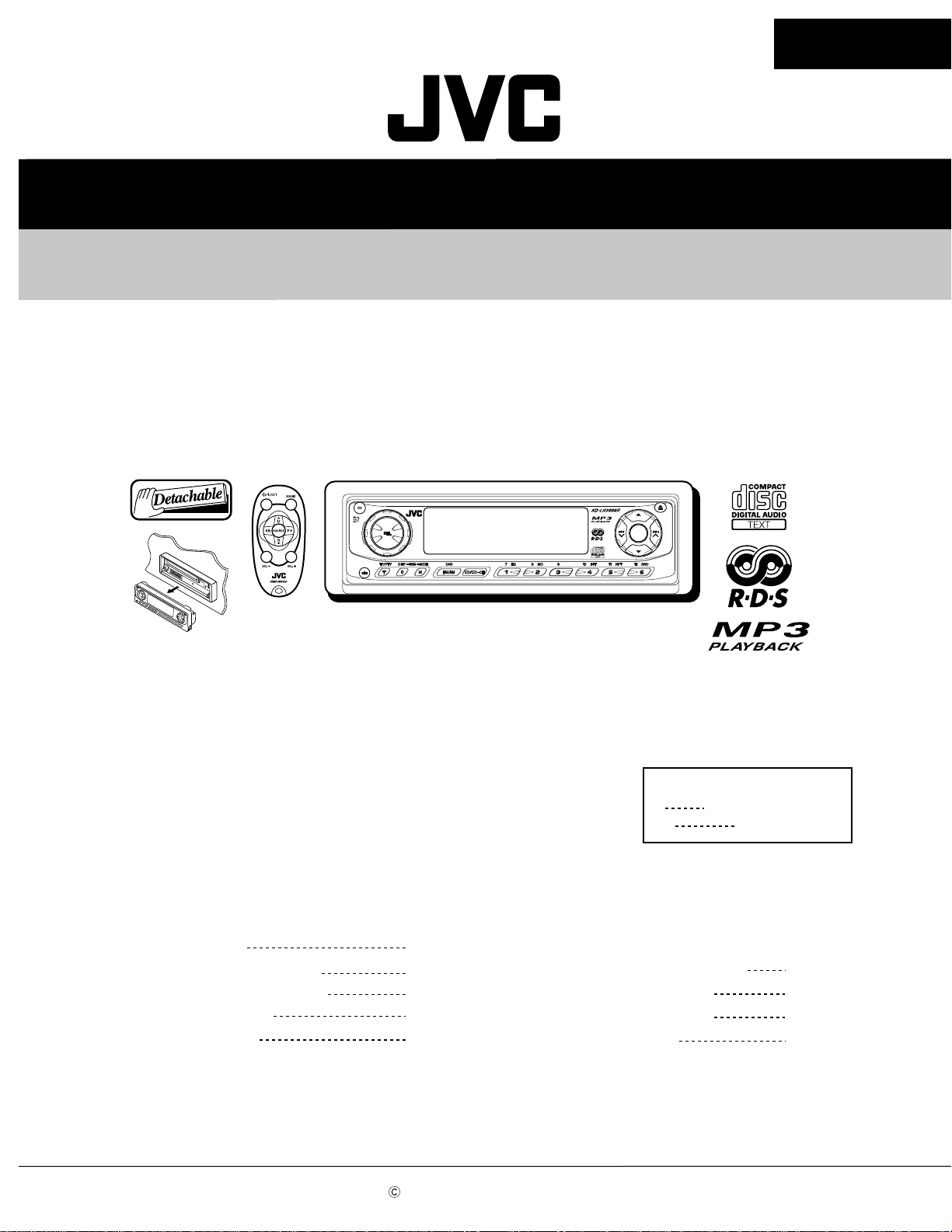
SERVICE MANUAL
CD RECEIVER
KD-LH2000R
KD-LH2000R
Contents
Safety precaution
Preventing static electricity
Important for laser products
Disassembly method
Adjustment method
1-2
1-3
1-4
1-5
1-20
COPYRIGHT 2002 VICTOR COMPANY OF JAPAN, LTD.
Flow of functional
operation unit TOC read
Maintenance of laser pickup
Replacement of laser pickup
Description of major ICs
E
EX
Area Suffix
Continental Europe
Central Europe
1-21
1-23
1-23
1-24~51
No.49753
Jun. 2002
Page 2
KD-LH2000R
Safety precaution
!
!
Burrs formed during molding may be left over on some parts of the chassis. Therefore,
pay attention to such burrs in the case of preforming repair of this system.
Please use enough caution not to see the beam directly or touch it in case of an
adjustment or operation check.
1-2
Page 3
KD-LH2000R
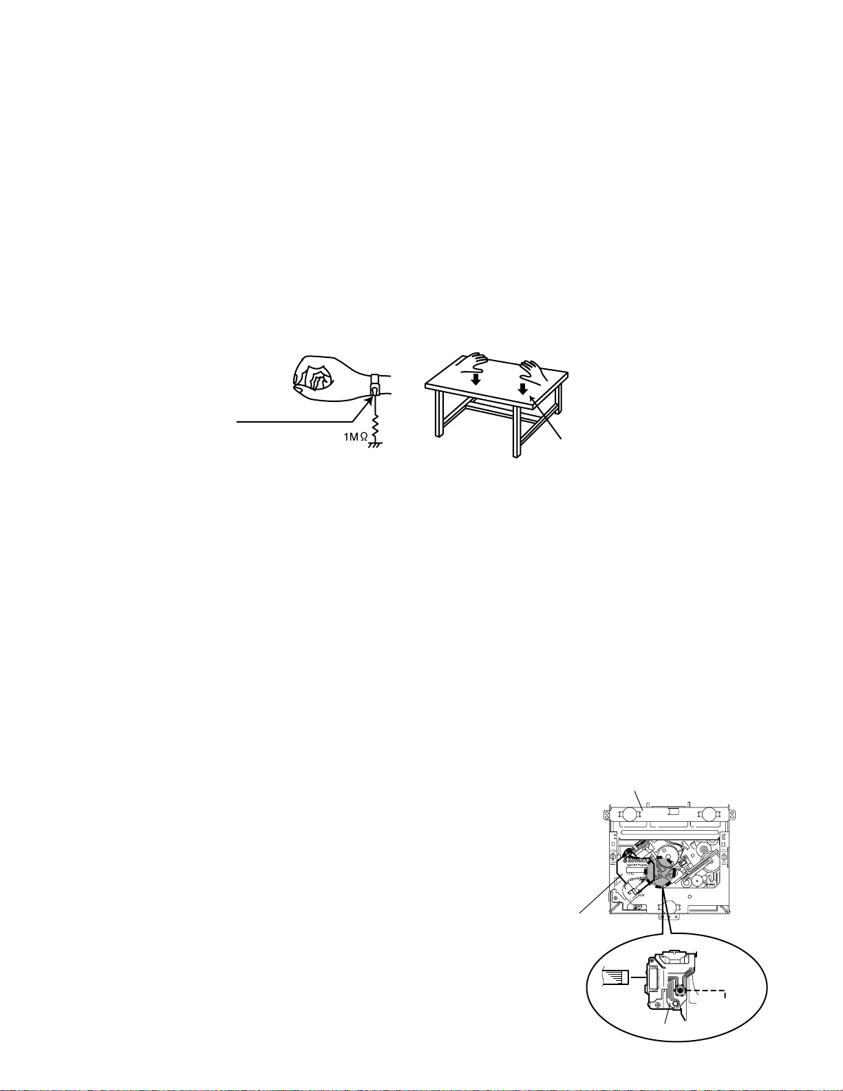
Preventing static electricity
1.Grounding to prevent damage by static electricity
Electrostatic discharge (ESD), which occurs when static electricity stored in the body, fabric, etc. is discharged,
can destroy the laser diode in the traverse unit (optical pickup). Take care to prev ent this when performing repairs.
2.About the earth processing for the destruction prevention by static electricity
Static electricity in the work area can destroy the optical pickup (laser diode) in devices such as CD players.
Be careful to use proper grounding in the area where repairs are being performed.
2-1 Ground the workbench
Ground the workbench by laying conductive material (such as a conductive sheet) or an iron plate over
it before placing the traverse unit (optical pickup) on it.
2-2 Ground yourself
Use an anti-static wrist strap to release any static electricity built up in your body.
(caption)
Anti-static wrist strap
Conductive material
(conductive sheet) or iron plate
3. Handling the optical pickup
1. In order to maintain quality during transport and before installation, both sides of the laser diode on the
replacement optical pickup are shorted. After replacement, return the shorted parts to their original condition.
(Refer to the text.)
2. Do not use a tester to check the condition of the laser diode in the optical pickup. The tester's internal power
source can easily destroy the laser diode.
4.Handling the traverse unit (optical pickup)
1. Do not subject the traverse unit (optical pickup) to strong shocks, as it is a sensitive, complex unit.
2. Cut off the shorted part of the flexible cable using nippers, etc. after replacing the optical pickup. For specific
details, refer to the replacement procedure in the text. Remove the anti-static pin when replacing the traverse
unit. Be careful not to take too long a time when attaching it to the connector.
3. Handle the flexible cable carefully as it may break when subjected to strong force.
4. It is not possible to adjust the semi-fixed resistor that adjusts the laser power. Do not turn it
CD mechanism ass’y
Attention when traverse unit is decomposed
*Please refer to "Disassembly method" in the text for pick-up and how to
detach the substrate.
1.Solder is put up before the card wire is removed from connector on
the CD substrate as shown in Figure.
(When the wire is removed without putting up solder, the CD pick-up
assembly might destroy.)
2.Please remove solder after connecting the card wire with
when you install picking up in the substrate.
CD mechanism
control board
Soldering
Pickup unit
1-3
Page 4
KD-LH2000R
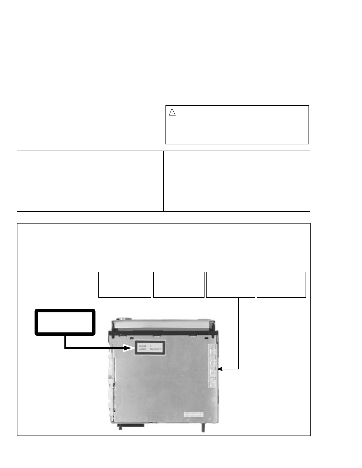
Important for laser products
1.CLASS 1 LASER PRODUCT
2.DANGER : Invisible laser radiation when open and inter
lock failed or defeated. Avoid direct exposure to beam.
3.CAUTION : There are no serviceable parts inside the
Laser Unit. Do not disassemble the Laser Unit. Replace
the complete Laser Unit if it malfunctions.
4.CAUTION : The compact disc player uses invisible
laserradiation and is equipped with safety switches
whichprevent emission of radiation when the drawer is
open and the safety interlocks have failed or are de
feated. It is dangerous to defeat the safety switches.
VARNING : Osynlig laserstrålning är denna del är öppnad
och spårren är urkopplad. Betrakta ej strålen.
VARO : Avattaessa ja suojalukitus ohitettaessa olet
alttiina näkymättömälle lasersäteilylle.Älä katso
säteeseen.
5.CAUTION : If safety switches malfunction, the laser is able
to function.
6.CAUTION : Use of controls, adjustments or performance of
procedures other than those specified herein may result in
hazardous radiation exposure.
CAUTION
!
Please use enough caution not to
see the beam directly or touch it
in case of an adjustment or operation
check.
ADVARSEL : Usynlig laserstråling ved åbning , når
sikkerhedsafbrydere er ude af funktion. Undgå
udsættelse for stråling.
ADVARSEL : Usynlig laserstråling ved åpning,når
sikkerhetsbryteren er avslott. unngå utsettelse
for stråling.
REPRODUCTION AND POSITION OF LABELS
WARNING LABEL
CLASS 1
LASER PRODUCT
DANGER : Invisibie laser radiation
when open and interlock or
defeated.
AVOID DIRECT EXPOSURE TO
BEAM (e)
VARO : Avattaessa ja suojalukitus
ohitettaessa olet alttiina
näkymättömälle lasersäteilylle.Älä
katso säteeseen. (d)
VARNING : Osynlig laserstrålning är
denna del är öppnad och spårren är
urkopplad. Betrakta ej strålen. (s)
ADVARSEL :Usynlig laserstråling
ved åbning , når
sikkerhedsafbrydere er ude af
funktion. Undgå udsættelse for
stråling. (f)
1-4
Page 5
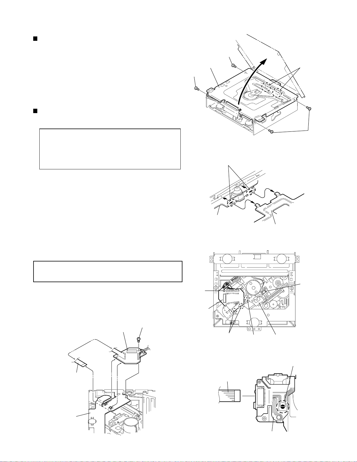
Disassembly method
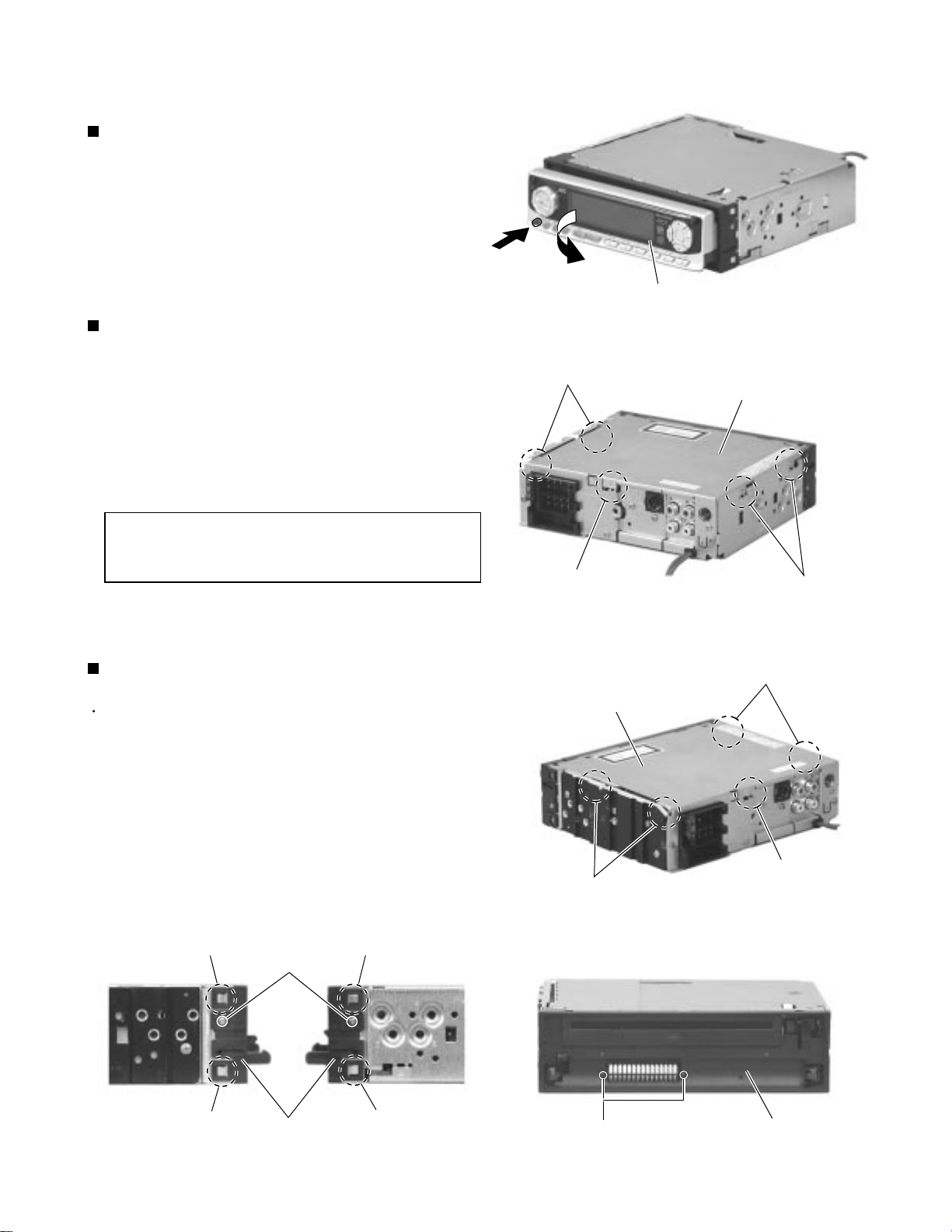
Removing the front panel unit
(See Fig.1)
1.
Press the release switch and remove the front panel
unit in the direction of the arrow.
KD-LH2000R
Front panel unit
Removing the bottom cover
(See Fig.2,3)
1.
Turn the body upside down.
2.
Insert a screwdriver to the two joints a and two joints
b on both sides of the body and the joint c on the
back of the body, then detach the bottom cover from
the body.
CAUTION:
When disengaging the joint c using a
screwdriver, do not damage or break the
board.
Removing the front chassis (See Fig.4,5)
Prior to performing the following procedure, remove
the bottom cover.
1.
Remove the two screws A attaching the front
chassis.
Joint a
Joint c
Bottom cover
Fig.1
Bottom cover
Joint b
Fig. 2
Joint b
2.
Remove the two screws B on each side of the body.
3.
Release the two joints d and the two joints e on the
sides. remove the front chassis toward the front.
Joint d
Joint e
B
Joint d
Front chassis
Fig. 5
Joint e
Joint a
A
Joint c
Fig. 3
Front chassis
Fig.4
1-5
Page 6
KD-LH2000R
Removing the heat sink (See Fig.6)
1.
Remove the four screws C attaching the heat sink
on the left side of the body, and remove the heat
sink.
Removing the rear panel (See Fig.7 )
C
C
Heat sink
Fig. 6
C
Prior to performing the following procedure, remove
the front chassis, the heat sink and bottom cover.
1.
Remove the six screws D attaching the rear panel
and one screw E attaching the pine jack on the back
of the body.
D
Rear panel
Removing the main amplifier board assembly
(See Fig.8)
Prior to performing the following procedure, remove
the front chassis, the heat sink, bottom cover and the
rear panel.
D
Fig. 7
E
D
D
1.
Remove the two screws F attaching the main
amplifier board assembly on the top cover.
2.
Disconnect connector CN601 on the main amplifier
board assembly from the cassette mechanism
assembly.
1-6
F
Main board assembly
F
CN601
Fig. 8
Page 7
KD-LH2000R
Removing the MP3 board
(See Fig.9)
Prior to performing the following procedure, remove
the top cover.
1.
Disconnect the wire from connector CN601on the
MP3 board.
2.
Remove the five screws G and the MP3 board,
releasing the joint f and g.
G
f
MP3 board
g
CN601
G
Fig.9
Removing the CD mechanism assembly
(See Fig.10)
Prior to performing the following procedure, remove
the front chassis, the heat sink, bottom cover and the
main amplifier board assembly.
1.
Remove the three screws H attaching the cassette
mechanism assembly from the top cover.
Top cover
H
H
H
CD mechanism assembly
Fig. 10
1-7
Page 8
KD-LH2000R
Removing the (LCD & key) control switch
board (See Fig.11
Prior to performing the following procedure, remove
the front panel assembly.
1.
Remove the four screws I attaching the rear cover
on the back of the front panel assembly.
2.
Unjoint the nine joints h with the front panel and the
rear cover.
3.
Remove the control switch board on the back of the
front panel.
~ 13)
I
I
Fig. 11
I
I
Front panel
Joint h
LCD & Key control board
Joint h
Rear cover
Joint h
Joint h
Fig. 12
1-8
Fig. 13
Page 9
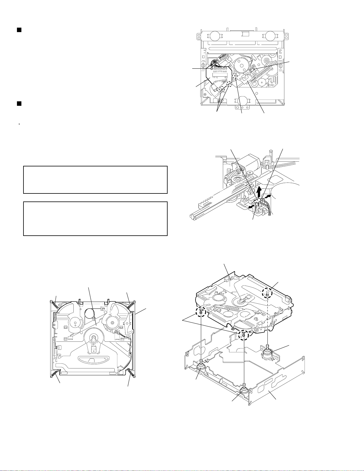
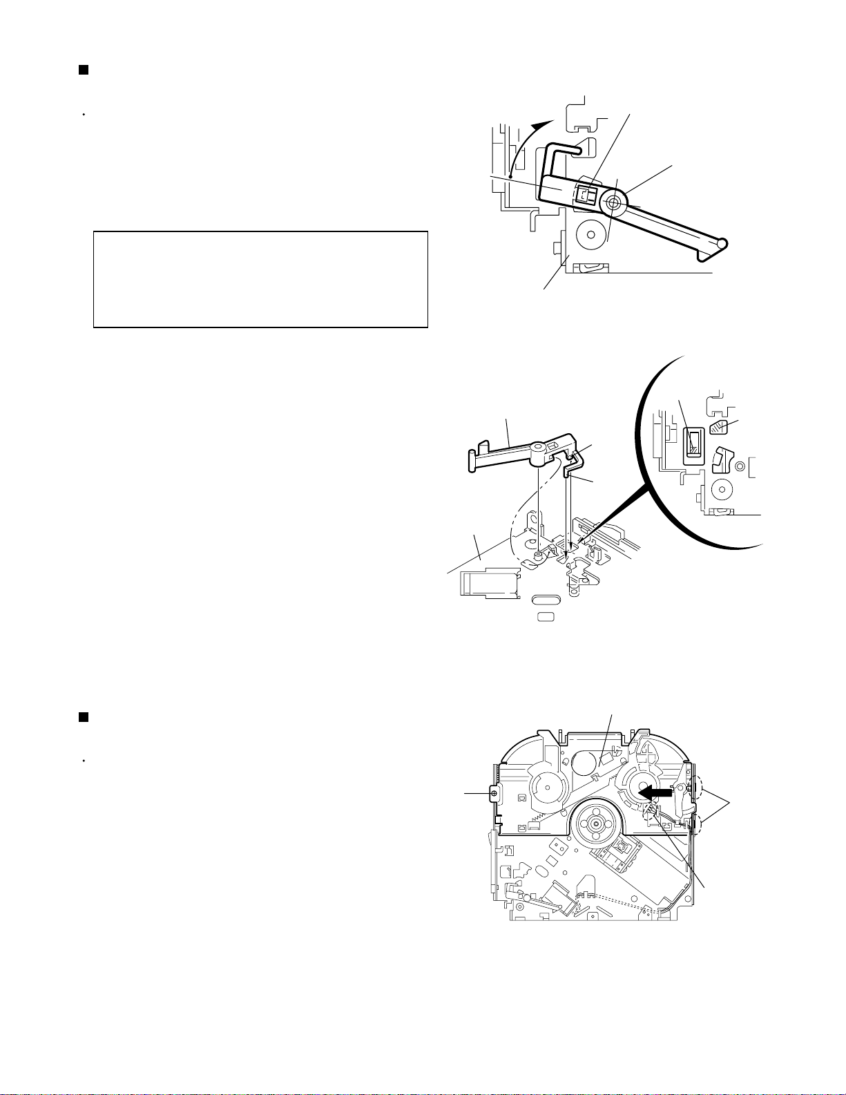
< CD mechanism section >
Removing the top cover
(See Fig.1 and 2)
1.
Remove the two screws A on each side of the body.
2.
Lift the front side of the top cover and move the
cover backward to release the two joints a.
Removing the connector board
(See Fig.3 to 5)
Top cover
A
KD-LH2000R
A
Joints a
CAUTION:
1.
Remove the screw B fixing the connector board.
2.
Solder the short-circuit point on the connector board.
Disconnect the flexible wire from the pickup.
3.
Move the connector board in the direction of the
arrow to release the two joints b.
4.
Unsolder the wire on the connector board if
necessary.
CAUTION:
Before disconnecting the flexible wire
from the pickup, solder the short-circuit
point on the pickup. No observance of
this instruction may cause damage of
the pickup.
Unsolder the short-circuit point after
reassembling.
A
Fig.1
Joints a
Top cover
Fig.2
DET switch
B
Flexible wire
Frame
Connector board
B
Connector board
Joints b
Flexible wire
Short-circuit
Fig.3
Fig.4Fig.5
Pickup
Short-circuit point
(Soldering)
Pickup
1-9
Page 10
KD-LH2000R
Removing the DET switch
(See Fig.3 and 6)
1.
Extend the two tabs c of the feed sw. holder and pull
out the switch.
2.
Unsolder the DET switch wire if necessary.
Removing the chassis unit
(See Fig.7 and 8)
Prior to performing the following procedure, remove
the top cover and the connector board.
B
Connector board
Joints b
Short-circuit
Fig.3
DET switch
Pickup
1.
Remove the two suspension springs (L) and (R)
attaching the chassis unit to the frame.
CAUTION:
The shape of the suspension spring (L)
and (R) are different. Handle them with
care.
CAUTION:
When reassembling, make sure that the
three shafts on the underside of the
chassis unit are inserted to the dampers
certainly.
Chassis unit
Suspension spring (R)
Suspension spring (L)
Frame
DET switch
Chassis unit
Tab c
Feed sw. holder
Tab c
Fig.6
Shaft
1-10
Suspension spring (R)
Suspension spring (L)
Shafts
Damper
Damper
Damper
Frame
Fig.8Fig.7
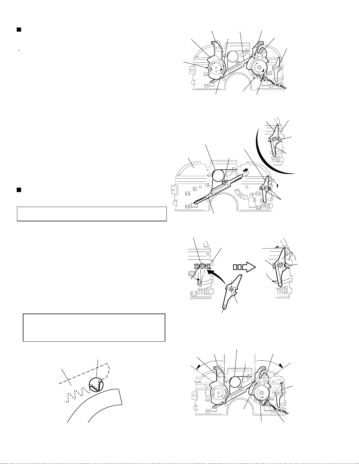
Page 11
Removing the clamper assembly
(See Fig.9 and 10)
KD-LH2000R
Prior to performing the following procedure, remove
the top cover.
1.
Remove the clamper arm spring.
2.
Move the clamper assembly in the direction of the
arrow to release the two joints d.
Removing the loading / feed motor
assembly (See Fig.11 and 12)
Prior to performing the following procedure, remove
the top cover, the connector board and the chassis
unit.
1.
Remove the screw C and move the loading / feed
motor assembly in the direction of the arrow to
remove it from the chassis rivet assembly.
Clamper arm
spring
Joint d
Joint d
Clamper assembly
Fig.9
Clamper arm spring
Chassis rivet
assembly
Joint d
Clamper assembly
Joint d
2.
Disconnect the wire from the loading / feed motor
assembly if necessary.
CAUTION:
When reassembling, connect the wire
from the loading / feed motor assembly
to the flame as shown in Fig.11.
Chassis rivet assembly
Fig.10
Loading / feed motor assembly
C
Loading / feed motor assembly
Fig.12Fig.11
1-11
Page 12
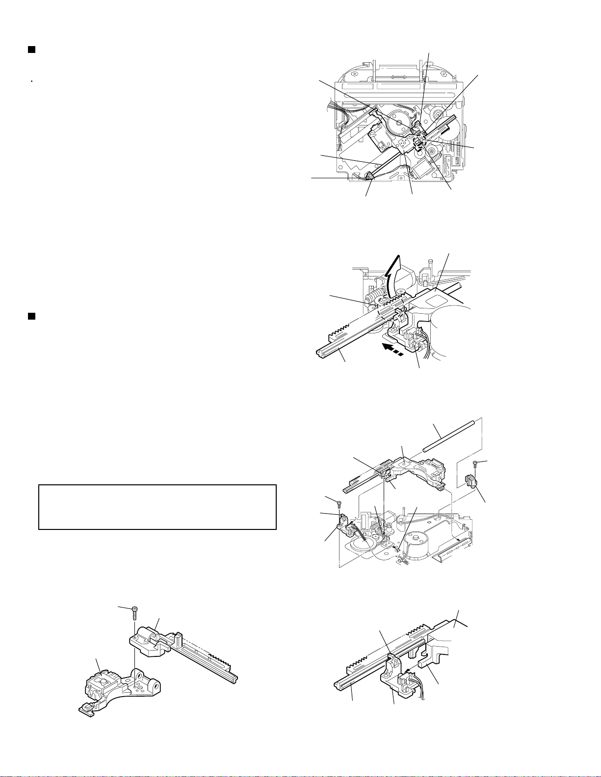
KD-LH2000R
Removing the pickup unit
(See Fig.13 to 17)
Prior to performing the following procedure, remove
the top cover, the connector board and the chassis
unit.
1.
Remove the screw D and pull out the pu. shaft
holder from the shaft.
2.
Remove the screw E attaching the feed sw. holder.
3.
Move the part e of the pickup unit upward with the
shaft and the feed sw. holder, then release the joint f
of the feed sw. holder in the direction of the arrow.
The joint g of the pickup unit and the feed rack is
released, and the feed sw. holder comes off.
4.
Remove the shaft from the pickup unit.
5.
Remove the screw F attaching the feed rack to the
pickup unit.
Reattaching the pickup unit
(See Fig.13 to 16)
Joint f
Shaft
D
Joint e
Pu. shaft holder
Feed sw. holder
Pickup unit
Fig.13
Pickup unit
E
Joint f
Joint e
1.
Reattach the feed rack to the pickup unit using the
screw F.
2.
Reattach the feed sw. holder to the feed rack while
setting the joint tab g to the slot of the feed rack and
setting the part f of the feed rack to the switch of the
feed sw. holder correctly.
3.
As the feed sw. holder is temporarily attached to the
pickup unit, set to the gear of the joint g and to the
bending part of the chassis (joint h) at a time.
CAUTION:
4.
Reattach the feed sw. holder using the screw E.
5.
Reattach the shaft to the pickup unit. Reattach the
pu. shaft holder to the shaft using the screw D.
Make sure that the part i on the underside
of the feed rack is certainly inserted to the
slot j of the change lock lever.
F
Feed rack
Feed rack
E
Joint g
Feed sw. holder
Part i
Pickup unit
Slot j
Joint g
Feed sw. holder
Fig.14
Shaft
Joint f
Joint h
Fig.15
D
Pu. shaft holder
Pickup unit
1-12
Pickup unit
Feed rack
Joint f
Feed sw. holder
Fig.17Fig.16
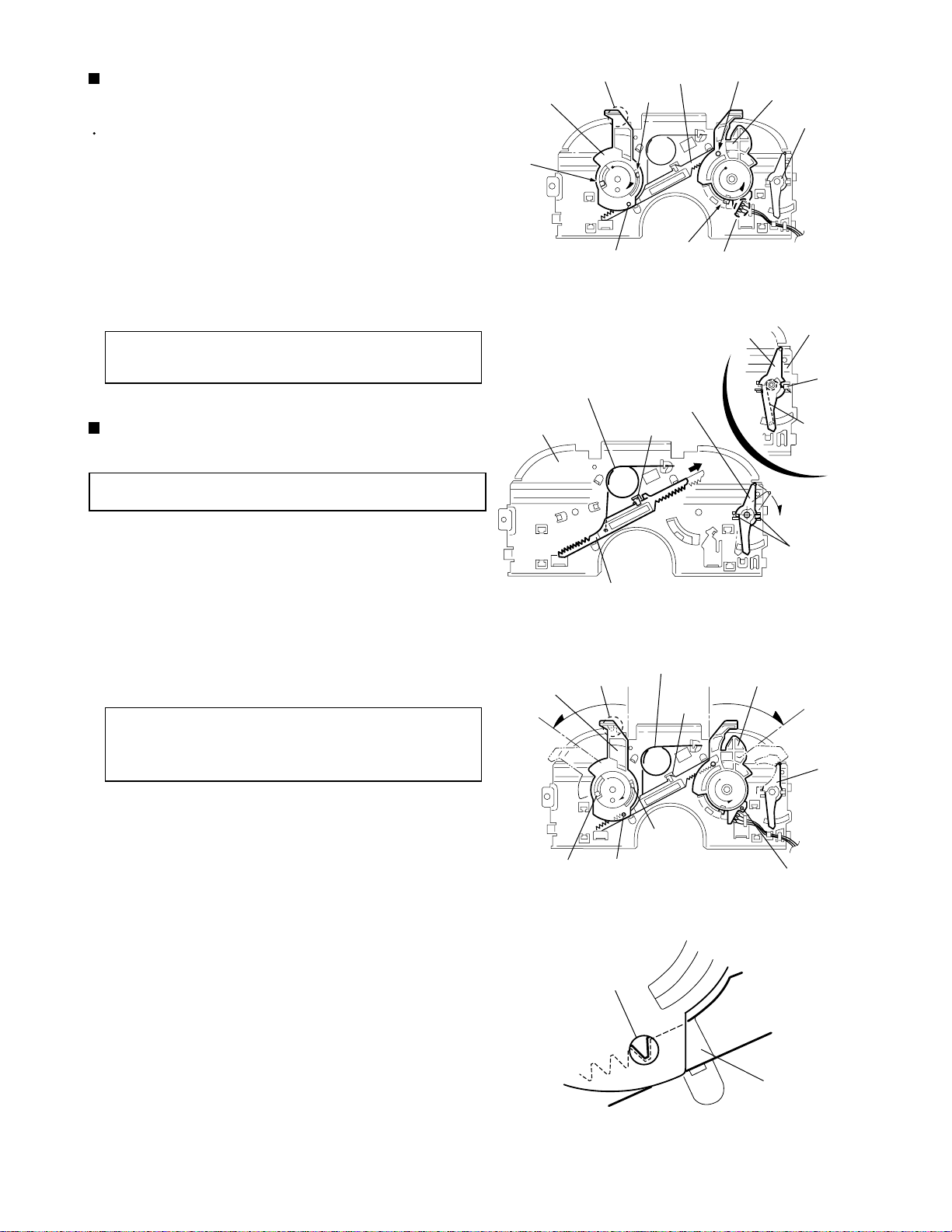
Page 13
Removing the trigger arm
(See Fig.18 and 19)
Prior to performing the following procedure, remove
the top cover, the connector board and the clamper
unit.
1.
Turn the trigger arm in the direction of the arrow to
release the joint k and pull out upward.
KD-LH2000R
Joint k
Trigger arm
CAUTION:
When reassembling, insert the part l and
m of the trigger arm into the part n and
o at the slot of the chassis rivet
assembly respectively and join the joint
k at a time.
Chassis rivet assembly
Chassis rivet assembly
Trigger arm
Fig.18
Part n
Part o
Part l
Part m
Fig.19
Removing the top plate assembly
(See Fig.20)
Prior to performing the following procedure, remove
the top cover, the connector board, the chassis unit,
and the clamper assembly.
1.
Remove the screw H.
2.
Move the top plate assembly in the direction of the
arrow to release the two joints p.
3.
Unsolder the wire marked q if necessary.
H
Top plate assembly
Joints p
q
Fig.20
1-13
Page 14
KD-LH2000R
Removing the select arm (L) / select lock
arm (See Fig.21 and 22)
Prior to performing the following procedure, remove
the top plate assembly.
1.
Bring up the select arm (L) to release from the link
plate (joint r) and turn in the direction of the arrow to
release the joint s.
2.
Unsolder the wire of the select arm (L) marked q if
necessary.
3.
Turn the select lock arm in the direction of the arrow
to release the two joints t.
The select lock arm spring comes off the select lock
arm at the same time.
Reassembling the select arm (L) / select
lock arm (See Fig.23 to 25)
Select arm (R)
Joint z
Link plate spring
Top plate
Joint a'
Joint y
Link plate
Joint z
Joint s
Fig.21
Select lock arm
Select lock arm
Joint b'
Joint r
Select arm (L)
Select lock arm
q
Top plate
Hook u
Select lock
arm spring
Joints t
REFERENCE:
1.
Reattach the select lock arm spring to the top plate
Reverse the above removing procedure.
and set the shorter end of the select lock arm spring
to the hook u on the top plate.
2.
Set the other longer end of the select lock arm spring
to the boss v on the underside of the select lock arm,
and join the select lock arm to the slots (joint t). Turn
the select lock arm as shown in the figure.
3.
Reattach the select arm (L) while setting the part r to
the first peak of the link plate gear, and join the joint
s.
CAUTION:
When reattaching the select arm (L),
check if the points w and x are correctly
fitted and if each part operates properly.
Joint r
Link plate
Link plate
Select lock arm spring
Boss v
Select arm (R)
Joint a'
Fig.22
Hook u
Joint t
Joint t
Select lock arm
Fig.23
Link plate spring
Select arm (L)
Joint b'
1-14
Joint r
Fig.25Fig.24
Joint s
Select
lock arm
Point x
Page 15
KD-LH2000R
Removing the select arm (R) / link plate
(See Fig.21 and 22)
Prior to performing the following procedure, remove
the top plate assembly.
1.
Bring up the select arm (R) to release from the link
plate (joint y) and turn as shown in the figure to
release the two joints z and joint a’.
2.
Move the link plate in the direction of the arrow to
release the joint b’. Remove the link plate spring at
the same time.
REFERENCE:
Before removing the link plate, remove
the select arm (L).
Reattaching the Select arm (R) / link
plate (See Fig.25 and 26)
REFERENCE:
Reverse the above removing procedure.
Select arm (R)
Joint z
Link plate spring
Top plate
Joint a'
Part y
Link plate
Joint z
Joint s
Fig.21
Select lock arm
Select lock arm
Joint b'
Joint r
Select arm (L)
Select lock arm
q
Top plate
Hook u
Select lock
arm spring
1.
Reattach the link plate spring.
2.
Reattach the link plate to the link plate spring while
joining them at joint b’.
3.
Reattach the part y of the select arm (R) to the first
peak of the link plate while joining the two joints z
with the slots. Then turn the select arm (R) as shown
in the figure. The top plate is joined to the joint a’.
CAUTION:
When reattaching the select arm (R),
check if the part c’ is correctly fitted and
if each part operates properly.
Select arm (R)
Joint z
Link plate
Link plate spring
Joint a'
Part y
Part y
Fig.22
Joint b'
Joint z
Fig.25
Joints t
Select arm (L)
Select
lock arm
Point x
Fig.26
Link plate
1-15
Page 16
KD-LH2000R
Removing the loading roller assembly
(See Fig.27 to 29)
Prior to performing the following procedure, remove
the clamper assembly and the top plate assembly.
1.
Push inward the loading roller assembly on the gear
side and detach it upward from the slot of the joint d’
of the lock arm rivet assembly.
Detach the loading roller assembly from the slot of
the joint e’ of the lock arm rivet assembly.
The roller guide comes off the gear section of the
loading roller assembly.
Remove the roller guide and the washer from the
shaft of the loading roller assembly.
2.
Remove the screw I attaching the lock arm rivet
assembly.
3.
Push the shaft at the joint f’ of the lock arm rivet
assembly inward to release the lock arm rivet
assembly from the slot of the slide plate. Extend the
lock arm rivet assembly outward and release the
joint g’ from the boss of the chassis rivet assembly.
The roller guide springs on both sides come off.
Roller guide
Washer
Loading roller assembly
Roller guide
Joint e'
Roller guide spring
Roller guide spring
Joint d'
Loading roller assembly
Roller guide spring
Lock arm rivet assembly
Fig.27
Loading roller assembly
Roller guide
spring
CAUTION:
When reassembling, reattach the left
and right roller guide springs to the lock
arm rivet assembly before reattaching
the lock arm rivet assembly to the
chassis rivet assembly. Make sure to fit
the part h’ of the roller guide spring (L)
inside of the roller guide (Refer to
Fig.30).
Roller guide
Washer
Roller shaft assembly
Joint h'
Loading roller assembly
Roller guide
spring
Fig.28-1
Fig.28-2
Chassis rivet assembly
Boss
Slide plate
Roller guide spring
I
1-16
Frame
Loading roller
Roller guide spring
Lock arm rivet assembly
Joint f'
Part g'
Fig.29Fig.30
Page 17

KD-LH2000R
Removing the loading gear (5), (6) and
(7) (See Fig.31 and 32)
Prior to performing the following procedure, remove
the top cover, the chassis unit and the top plate
assembly.
1.
Remove the screw J attaching the loading gear
bracket. The loading gear (6) and (7) come off the
loading gear bracket.
2.
Pull out the loading gear (5).
Loading gear bracket
J
Loading gear (6)
Loading gear (5)
Loading gear (3)
Fig.31
J
Loading gear bracket
Loading gear (5)
Loading gear (6)
Loading gear (7)
Fig.32
1-17
Page 18

KD-LH2000R
Removing the gears (See Fig.33 to 36)
Prior to performing the following procedure, remove
the top cover, the chassis unit, the top plate
assembly and the pickup unit.
1.
Pull out the feed gear.
Slot j'
Slide plate
2.
Move the loading plate assembly in the direction of
the arrow to release the slide plate from the two slots
j’ of the chassis rivet assembly.
3.
Detach the loading plate assembly upward from the
chassis rivet assembly while releasing the joint k’.
Remove the slide hook and the loading plate spring
from the loading plate assembly.
4.
Pull out the loading gear (2) and remove the change
lock lever.
5.
Remove the E-washer and the washer attaching the
changer gear (2).
6.
The changer gear (2), the changer gear spring and
the adjusting washer come off.
7.
Remove the loading gear (1).
8.
Move the hang plate rivet assembly in the direction
of the arrow to release from the three shafts of the
chassis rivet assembly upward.
9.
Detach the loading gear plate rivet assembly from
the shaft of the chassis rivet assembly upward while
releasing the joint l’.
Feed gear
Change plate
rivet assembly
Shafts
E-washer
Loading plate assembly
Joint k'
Slot j'
Fig.33
Joint l'
Loading gear (4)
Loading gear plate
rivet assembly
Loading gear (2)
Loading gear (1)
Change gear (2)
10.
Pull out the loading gear (4).
Loading plate assembly
Loading plate spring
Slot j'
Chassis rivet assembly
Joint k'
Slide hook
Slide plate
Slot j'
E-washer
Washer
Loading gear (2)
Loading plate spring
Adjusting washer
Change plate
rivet assembly
Chassis rivet assembly
Fig.34
Loading gear (1)
Loading gear (2)
Change lock lever
Loading gear (4)
Loading gear plate rivet assembly
Fig.36Fig.35
1-18
Page 19

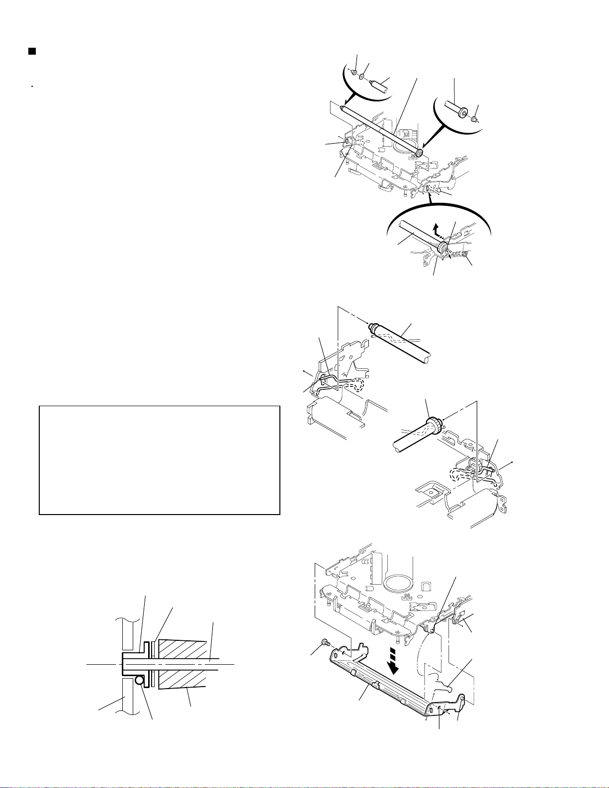
KD-LH2000R
Removing the turn table / spindle motor
(See Fig.37 and 38)
Prior to performing the following procedure, remove
the top cover, the connector assembly and the
chassis / clamper assembly.
1.
Remove the two screws K attaching the spindle
motor assembly through the slot of the turn table on
top of the body.
2.
Unsolder the wire on the connector board if
necessary.
K
Turn table
Fig.37
K
Turn table
Spindle motor
Fig.38
1-19
Page 20

KD-LH2000R
Adjustment method
Test instruments required for adjustment
1. Digital oscilloscope (100MHz)
2. AM Standard signal generator
3. FM Standard signal generator
4. Stereo modulator
5. Electric voltmeter
6. Digital tester
7. Tracking offset meter
8. Test Disc JVC :CTS-1000
9. Extension cable for check
EXTSH002-22P 1
Standard measuring conditions
Power supply voltage : DC14.4V(11V~16V allwance)
Load impedance : 4 (4 to 8 allowance)
Line-out Level / Impedance:
2.0V / 20 k load
How to connect the extension cable for adjusting
Standard volume position
Balance and Bass &Treble volume : lndication"0"
S.BASS : O
EQ : FLAT
Frequency Band
FM 87.5MHz ~ 108.0MHz
AM (MW) 522kHz ~ 1620 kHz
(LW) 144kHz ~ 279 kHz
Dummy load
Exclusive dummy load should be used for AM,and FM. For
FM dummy load,there is a loss of 6dB between SSG output
and antenna input.The loss of 6dB need not be considered
since direct reading of figures are applied in this working
standard.
Extension cables
EXTSH002-22P
CN601
Doing such as cardboard puts finishing
between the main body and mechanism.
fixes with rubber band.
1-20
Page 21

Flow of functional operation unit TOC read
Power ON
When the pickup correctly moves
v
to the inner area of the disc
Set Function CD
KD-LH2000R
When the laser diode correctly
emits
Microprocessor
commands
FMO
TC94A14FA" 40"
FEED MOTOR
+TERMINAL
IC681
REST SW
When correctly focused
FEO
TA2157" 15"
Focus Servo Loop ONo
$83
$82
$81
3.3V
Hi-Z
0V
6V
4V
2V
OFF
ON
Pickup feed to the inner area
2.2V
RF signal eye-patternn
remains closed
RF signal eye-pattern
opens
Disc inserted
YES
Laser emitted
Focus search
Disc rotates
Tracking loop closed
TOC read out
YES
Microprocessor
commands
SEL
TC94A14FA"38"
LD
CN601"8"
"No disc"
display
When the disc correctly rotates
Microprocessor
commands
DMO
TC94A14FA"41"
Spindle
motor(-)
IC681"7"
$84 $86 $ A200
Acceleration Servo CLV
Rough
Servo
0.5 Sec 0.5 Sec
$84
3.3V
0V
2V
0V
3.3V
2.2V
0V
6V
3.2
2V
Jump to the first track
Play
Tracking Servo Loop ON
RF signal
Rough Servo Modev
CLV Servo Mode
(Program Area)
CLV Servo Mode
(Lead-In Area;
Digital :0)
1-21
Page 22

KD-LH2000R
Feed section
Is the voltage output at
IC621 pin "40" 3.3V or 0V?
YES
Is 4V present at both
sides of the feed motor?
YES
NO YES NO
NO
Is the wiring for IC621
(56)~(64) correct?
NO
Is 6V or 2V present at
IC681 "4" and "5"?
NO
Is 3.3V present at IC681
pin "20"?
Check the vicinity of
IC621.
YES
Check the feed motor
connection wiring.
YES
Check CD 8V
and 5V.
Check the feed motor.
Focus section
When the lens is
moving:
4V
Does the S-search
waveform appear at
IC681 pins "10" and "11"?
Spindle section
Is the disk rotated?
YES
Does the RF signal
appear at TP1?
YES
Is the RF waveform at TP1
distorted?
YES
Proceed to the Tracking
section
Check IC681.
NO
YES
NO
NO
NO
Check the circuits in
the vicinity of IC681
pins "10","11"and"14".
Check the pickup and
its connections
Is 4V present at IC681
pins "6" and "7"?
Check the spindle motor
and its wiring
Check the circuits in the
vicinity of IC601 "19"~
"24" or the pickup
YES
YES
NO
Is 3.3V present at IC621
pins "41" ?
Check the vicinity of
IC681.
NO
YES
Check IC621 and
IC601.
Tracking section
1-22
When the disc is rotated
at first:
Approx. 1.2V
Is the tracking error signal
output at IC601 "11"?
YES
Check IC621.
YES YES
Check the circuit in the
vicinity of IC601 pins
"2"~"12".
Check the pickup and
its connections
Page 23

Maintenance of laser pickup
(1) Cleaning the pickup lens
Before you replace the pickup,please try to
clean the lens with a alcohol soaked cotton
swab.
(2) Life of the laser diode
When the life of the laser diode has expired.
the following symptoms will appear..
(1) The level of RF output (EFM output:amplitude
of eye patterrn) will be low.
KD-LH2000R
Is RF output
1.3 0.4Vp-p?
YES
O.K
(3) Semi-fixed resistor on the APC PC board
The semi-fixed resistor on the APC printed
circuit board which is attached to the pickup
is used to adjust the laser power.Since this.
adjustment should be performed to match the
characteristics of the whole optical block,
do not touch the semi-fixed resistor..
If the laser power is lower than the specified
value, the laser diode is almost worn out, and
the laser pickup should be replaced.
If the semi-fixed resistor is adjusted while
the pickup is functioning normally, the laser
pickup may be damaged due to excessive current.
NO
Replace it.
Replacement of laser pickup
Turn of the power switch and, disconnect the
power cord.
Replace the pickup with a normal one.(Refer
to "Pickup Removal" on the previous page)
Plug the power cord in, and turn the power on.
At this time, check that the laser emits for
about 3seconds and the objective lens moves
up and down.
Note: Do not observe the laser beam directly..
Play a disc.
Check the eye-pattern at TP1.
Finish.
1-23
Page 24

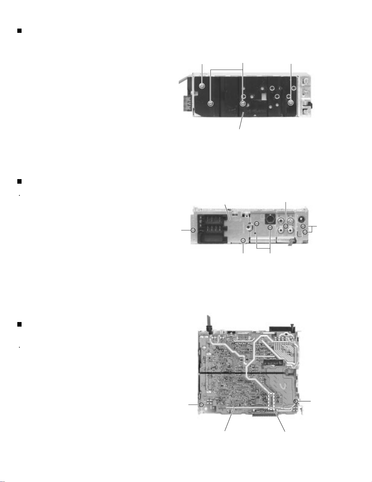
KD-LH2000R
Description of major ICs
UPD784215AGC179 (IC701) : CPU
1.
Pin
layout
75 ~ 51
76
~
100
1 ~ 25
50
~
26
2. Pin function
Pin NO. Symbol Function
1~7
8
9
10
11
12
13
14
15
16
17
18
19
20
21
22
23
24
25
26
27
28
29
30
31
32
33
34
35
36
37
38
39
40
41~43
44
45
46
47
48
49~52
53
NC
ANT CONT
VDD
X2
X1
VSS
XT2
XT1
RESET
NC
BUS-INT
PS2
CD-REQ
RDS-SCK
RDS DA
KEY DATA
AVDD
AVREF0
VOL1
VOL2
KEY1
KEY2
NC
MRC
SQ
SM
AVSS
NC
STAGE3
AVREF
BUS-SI
BUS-SO
BUS-SCK
BUS-I/O
NC
BUZZER
E2PROM-DI
E2PROM-DO
E2PROM-CLK
OPEN
NC
SD/ST
I/O
-
Antenna remote control
O
Maicon power supply
I
I
O
GND
I
I
O
SYSTEM RESET
I
-
J-BUS INT
I
Power save2, H means STOP mode
I
CD REQ INPUT
I
RDS clock input
I
RDS data input
I
KEY DATA
I
A/D converter power supply
I
A/D reference voltage
O
Volume encoder pulse input 1
I
Volume encoder pulse input 2
I
Handle remocon input 1
I
Handle remocon input 2
I
-
MRC input
I
S.Quality level input
I
S.METER input
I
GND
I
-
Feature selection H:2000 L:1000
I
I
J-BUS data input
I
J-BUS data output
O
J-BUS clock input / output
I/O
J-BUS I/O selection output:H, input:L
O
-
Buzzer output
O
I2C data input
I
I2C data output
O
I2C clock output
O
DOOR OPEN SW
I
-
Station detector or streo indica tor i nput ;
I
H means a station is there. L means the program is stereo.
1-24
Page 25

KD-LH2000R
Pin NO. Symbol Function
54~56
57
58
59
60
61
62
63
64
65
66
67
68
69
70
71
72
73
74
75
76
77
78
79
80
81
82
83
84
85
86
87
88
89
90
91~93
94
95~98
99
100
NC
DISP SCK
DISP DA
DISP CE
NC
DETACH
AFCK
SEEK/STOP
CF SEL
FM/AM
PLL-CE
PLL-DO
PLL-CLK
PLL-DI
TEL-MUTING
DIM-OUT
VSS
DIM-IN
PS1
POWER
NC
MUTING
CD MUTING
CD RESET
NC
VDD
NC
VOL-DA
VOL-CLK
NC
SUB MUTING
LPF 1
LPF 2
STAGE2
STAGE1
NC
TEST
NC
DISC SEL
NC
I/O
-
DISPLAY SCK
O
DISPLAY DATA
O
DISPLAY CE
O
-
Detach detect input ; H m eans detaching
I
AF check output
O
Auto seek and stop selecting output ; H mea ns seek i ng, L means receiving.
O
Wide & Narrow
O
FM, AM band selecti ng output ; H = FM,L= AM
O
CE output for PLL IC
O
Data output for PLL IC
O
Clock output for PLL IC
O
Data input from PLL IC
I
Telphone muting detection input ;
I
Active level can be selected H or L in PSM
Dimmer detector output
O
GND
I
Dimmer detector input L=dimmer on
I
POWER SAVE1 L= ACC off
I
POWER ON/OFF control output H=power on
O
-
Muting output L=muting on
O
CD MUTE INPUT L=MUTE ON
I
CD RESETCONTROL OUT H=RESET ON
O
-
Maicon power supply
I
-
Data output for e-vol IC
O
Clock output for e-vol IC
O
-
Muting control output for subwoofer
O
LPF CONTROL 1
O
LPF CONTROL 2
O
Feature selection H:R or Do L:J or U
I
Feature selection H:R or U L:J or Do
I
-
For rewriting flash memory
I/O
-
8cmCD SELECT L=NO USE H=USE
O
-
-
1-25
Page 26

KD-LH2000R
UPD784225GK-626 (IC501) : CPU
1.Pin layout
80 ~ 61
1 ~ 20
21 ~ 40
2.Pin function
Pin
Symbol
no.
1
TEMP
2
GND
3
GND
4
AVSS
5
ADCONT
6
NC
7
AVREF1
8
EPROMDI
9
EPROMDO
10
EPROMCK
11
LCDCE/SO
12
LCDDA/SI
13
LCDCK
14
/BUSIO
15
BUSIO
16
BUSSI
17
BUSSO
18
BUSSCK
19
BUSOUT
20
CDON
21
CDREQ
22
CDMUTE
23
NC
24
DSPRESET
25
CCE
26
BUCK
27
BUS3
28
BUS2
29
BUS1
30
BUS0
31
2XPLAY
32
RWSEL
33
VSS1
34
LOAD
35
LD/FE
36
MP3DI
37
MP3DO
38
MP3CK
39
MP3RESET
40
MPSSTB
60 ~ 41
I/O
Connect to TEMP detecter
I 41
Connect to GND
-
Connect to GND
-
Connect to GND
-
No use
-
No use
-
Analog reference voltage
-
Data input terminal from EEPROM
I
Data output terminal from EEPROM
O
Clock signal I/O terminal with EEPROM
I/O
No use
-
No use
-
No use
-
J-BUS data I/O terminal
I/O
J-BUS data I/O terminal
I/O
J-BUS data input
I
J-BUS data output
O
J-BUS clock I/O
I/O
No use
-
The CD power supply control signal output.At CD:H
O
CD request
I
CD Mute
O
No use
-
DSP reset
O
CE output for data communication with CDLSI
O
Clock output for data communication with CDLSI
O
Data communication input output port 3 with CDLSI
I/O
Data communication input output port 2 with CDLSI
I/O
Data communication input output port 1 with CDLSI
I/O
Data communication input output port 0 with CDLSI
I/O
No use
-
CD RW select
I
Connect to GND
-
Loading signal
O
LDFLE switching signal
O
MP3 data input
I
MP3 data output
O
MP3 data clock
O
MP3 data reset
O
MP3 data standby
I
Function Function
Pin
no.
42
43
44
45
46
47
48
49
50
51
52
53
54
55
TEST MODE
56
57
58
59
60
61
62
63
64
65
66
67
68
69
70
71
72
73
74
75
76
77
78
79
80
Symbol
NC
NC
NC
DACML
DACMC
DACMD
DACCS
NC
NC
NC
NC
DISCSEL
DACSEL
NC
MP3SEL
8VDET
REST
SW2
RESET
SW1
B.DET
P.DET
BUSINT
MP3REQ
NC
VSS0
VDD1
X2
X1
VPP
XT2
XT1
VDD0
AVDD
IOP
KEY0
KEY1
KEY2
KEY3
I/O
Non use
-
Non use
-
Non use
-
DAC mode control latch
O
DAC mode control clock
O
DAC mode control data
O
DA convertor chip select
I
No use
-
No use
-
No use
-
No use
-
Initial setting
O
DA convertor select
O
No use
-
Connect to GND
-
MP3/CD-DA switch SW L:CD H:MP3
O
8V detection
I
System reset signal input
I
Detection switch of CD mechanism
I
Reset detection terminal
Detection switch of CD mechanism
I
Panel switch detection
I
Power switch detection
I
J-BUS signal interrupt input
I
MP3 request
O
No use
-
Connect to ground
-
Reference voltage terminal
-
No use
-
Connect to X'tal osc.
I
Test terminal
I
Non use
-
Connect to ground
-
Connect to ground
-
Reference voltage terminal
-
Laser signal input output
I/O
Key control signal input 0
I
Key control signal input 0
I
Key control signal input 0
I
Key control signal input 0
I
1-26
Page 27

2.Pin functions (2/2)
KD-LH2000R
Pin No.
47
48~51
52
53
54
55
56
57
58
59
60
61
62
63
64
65
66
67
68
69
70
71
72
73
74
75
76
77
78
79
80
Symbol
DAC CS
-
DISC SEL
DAC SEL
-
TEST MODE
MP3 SEL
8V DET
REST
SW2
RESET
SW1
B.DET
P.DET
BUS INT
MP3 REQ
VSS0
VDD1
X2
X1
VPP
XT2
XT1
VDD0
AVDD
IOP
KEY0
KEY1
KEY2
KET3
I/O
O
I
I
I
I
I
I
I
I
I
I
I
I
I
-
-
-
O
I
-
O
I
-
I
I
I
I
I
Function
DAC chip select terminal
No use
8cm disc correspondence mode select terminal (respondance:L)
DAC select mode input terminal
LCD/AD key/Remocon invalid select mode input terminal L:invalid
MP3 select mode input terminal
CD mechanism power supply detection terminal (L:8V on)
CD mechanism rest switch input terminal
CD mechanism SW2 input terminal
Riset signal input terminal
CD mechanism SW1 input terminal
Backup power supply detection input terminal (H:Stop mode)
Main power off detection input terminal (H:HALT mode)
JVC BUS communication start squeeze input terminal
CD MP3 request signal input terminal
Connect to GND
Connect to 3.3V
Oscillator (6MHz)
Oscillator (6MHz)
Connect to GND
Open
Connect to GND
Connect to 3.3V
Connect to ADCONT
Pickup IOP measurement input terminal
Key input 0 (8bit A/D input) terminal
Key input 1 (8bit A/D input) terminal
Key input 2 (8bit A/D input) terminal
Key input 3 (8bit A/D input) terminal
1-27
Page 28

KD-LH2000R
BR24C01AFV-W (IC502) : EEPROM
1.Pin layout
2.Block diagram
1
A0
A1
2
Vcc WPIN SCL
SDA
A0 A1 A2 GND
1kbit EEPROM ARRAY
7bit
ADDRESS
DECODER
SLAVE/WORD
7bit
ADDRESS REGISTER
8bit
DATA
REGISTER
8
7
Vcc
WPIN
A2
3
GND
4
3.Pin function
Pin name I/O
Vcc
GND
A0,A1,A2
SCL
SDA
CONTROL LOGIC
HIGH VOLTAGE GEN.
-
IN
IN
IN / OUT
START
STOP
ACK
Vcc LEVEL DETECT
Function
Power supply
Ground (0v)
Slave address set
Serial clock input
Slave and word address,
serial data input, serial data output *1
SCL
6
SDA
5
1-28
WPIN
*1 An open drain output requires a pull-up resister.
IN
Write protect input
Page 29

HA13164A (IC901) : Regulator
1.Terminal layout
EXT
ANT
ACC
VDD
SW5V
ACC5V
ANT.CTRL
MEMORY
123456789101112131415
BATT.DET9VCTRL
CD8VAJILMI
KD-LH2000R
GND
2.Block diagram
ANT OUT
C3
0.1u
EXT OUT
C4
0.1u
ANT CTRL
CTRL
CD OUT
C5
0.1u
AUDIO OUT
C6
10u
11
12
10
BATT.DET OUT
9
COMPOUT
6
VDD OUT
4
SW5VOUT
5
14
UNIT R:
+B
ACC
ILMOUT
R1
C7
0.1u
C8
0.1u
C1
100u
VCC ACC
8
2
1
7
Surge Protector
BIAS TSD
15
3
TAB
note1) TAB (header of IC)
connected to GND
ILM AJGND GND
13
C2
0.1u
C:F
3.Pin function
Pin No. Symbol Function
1
2
EXT
ANT
Output voltage is VCC-1 V when M or H level applied to CTRL pin.
Output voltage is VCC-1 V when M or H level to CTRL pin and H level
to ANT-CTRL.
3
4
5
6
7
8
9
10
11
12
13
14
15
ACC
VDD
SW5V
COMP
ANT CTRL
MEMORY
BATT DET
9V
CTRL
CD8V
AJ
ILMI
GND
Connected to ACC.
Regular 5.7V.
Output voltage is 5V when M or H level applied to CTRL pin.
Output for ACC detector.
L:ANT output OFF , H:ANT output ON
Connected to VCC.
Low battery detect.
Output voltage is 9V when M or H level applied to CTRL pin.
L:BIAS OFF, M:BIAS ON, H:CD ON
Output voltage is 8V when H level applied to CTRL pin.
Adjustment pin for ILM output voltage.
Output voltage is 10V when M or H level applied to CTRL pin.
Connected to GND.
1-29
Page 30

KD-LH2000R
HD74HC126FP-X (IC781) : Buffer
1.Terminal layout
1C
1
1A
2
1Y
3
2C
4
2A
5
2Y
6
GND
7
2.Block diagram
Input
VU
14
4C
13
4A
12
4Y
11
3C
10
3A
9
3Y
8
Vcc Vcc
1A
2A
3A
4A
1C
2C
3C
See Function Table
4C
3.Pin function
Output
1Y
2Y
Output
2Y
Output
3Y
Output
4Y
Input
C
L
H
H
A
X
L
H
Output
Y
Z
H
L
Note) H:High level
L:Low level
X:Irrelevant
Z:Off(High-impedance)
State a 3-state input
1k
S1
CL
1k
Sample as Load Circuit 1
Sample as Load Circuit 1
Sample as Load Circuit 1
1-30
Note) CL includes probe and jig capacitance
Page 31

HD74HCT126T : (IC503) Buffer
KD-LH2000R
1.Terminal layout
Vcc
14
1
1C
2.Block diagram
4C
13
2
1A
3
1Y
1A
4A
12
4Y
11
4
2C
3C
10
5
2A
3A
9
6
2Y
3Y
8
7
GND
3.Pin function
INPUT
C
L
H
H
H : High level
L : Low level
X : Irrelevant
Off (Hhigh-impedance)state of a 3-stage
Z :
output
OUTPUT
A
X
L
H
Y
Z
H
L
1C
2A
2C
3A
3C
4A
1Y
2Y
3Y
4C
4Y
1-31
Page 32

KD-LH2000R
IC-PST9322U-X (IC803) : Regulator
1. Pin layout
2. Block diagram
NC 1
GND 2
3. Pin function
Pin No.
1
2
3
4
Symbol
GND
VOUT
Vcc
4 Vcc
3 VOUT
Function
NC
Non connect
GND terminal
Reset signal output terminal
Vcc terminal/Voltage detect terminal
Vcc 4
NC 1
3 VOUT
2 GND
IC-PST9333U-X (IC702) : Regulator
1. Pin layout
NC 1
GND 2
3. Pin function
Pin No.
1
2
3
4
Symbol
GND
VOUT
Vcc
4 Vcc
3 VOUT
Function
NC
Non connect
GND terminal
Reset signal output terminal
Vcc terminal/Voltage detect terminal
Vcc 4
NC 1
2. Block diagram
3 VOUT
2 GND
1-32
Page 33

M61508FP-X (IC111) : E. volume
1. Pin layout & Block diagram
VCC
(Analog)
2. Pin function
Pin No.
1
2
3
DEFP IN1
DEFN IN1
4
5
6
7
8
9
DEFN OUT1
SEL OUT1
10
11
12
13
14
15
TONE OUT1
FADER IN1
REAR OUT1
FRONT OUT1
NonFader OUT1
16
17
18
19
VDDOUT1
VDDOUT2
20
21
22
NonFader OUT2
23
24
25
26
FRONT OUT2
REAR OUT2
FADER IN2
TONE OUT2
27
28
29
SEL OUT2
DEFN OUT2
30
31
32
33
34
35
DEFN IN2
DEFP IN2
36
REF
Symbol Function
REF
Grand for IC signal
Differential motion amp. Positive terminal
Differential motion amp. Negative terminal
INA1
INB1
INC1
IND1
Input terminal of input selector switch channel 1
Input terminal of input selector switch channel 1
Input terminal of input selector switch channel 1
Input terminal of input selector switch channel 1
Differential output terminal (-)
Input selector output terminal
VOL IN1
Volume 1 input terminal
Tone output terminal
Volume 2 input terminal
Fader volume control (Rear) output terminal
Fader volume control (Front) output terminal
Non fader volume output terminal
GND
DATA
GND terminal
Control data input terminal
Test terminal
Test terminal
CLOCK
VDD
Clock input terminal for serial data transport
Power supply terminal for digital
Non fader volume control output terminal
Fader volume (Front) output terminal
Fader volume (Rear) output terminal
Volume 2 input terminal
Tone output terminal
VOL IN2
Volume 1 input terminal
Input selector output terminal
IND2
INC2
INB2
INA2
VCC
Input terminal of input selector switch channel 2
Input terminal of input selector switch channel 2
Input terminal of input selector switch channel 2
Input terminal of input selector switch channel 2
Power supply terminal
50K
27282930313233343536
LOUDNESS
+
3BAND TONE CONTROL
(BASS/MID/TREBLE)
ZERO CROSS
DETECTOR
ZERO CROSS
DETECTOR
LOUDNESS
+
3BAND TONE CONTROL
(BASS/MID/TREBLE)
A
B
B
A
2526
Zero detect
Select SW
121110987654321
24 23 22 21 20 19
VDO
(Digital)
Soft select
12dB
I/F
12dB
TIMER
DETECTOR
GND
13 14 15 16 17
KD-LH2000R
18
1-33
Page 34

KD-LH2000R
LA6579H-X (IC681) : 4-Channel bridge driver
1. Pin layout & Block diagram
VIN1-A
VIN1+A
VCCP1
1
+
2
3
VIN1_SW
[H]: OP-AMP_A
[L]: OP-AMP_B
[H]
[L]
28
VIN1
27
VIN1-B
-
+
26
VIN1+B
VO1+
VO1-
VO2+
VO2-
GND
VO3+
VO3-
VO4+
4
5
6
7
FR
8
9
10
Power system
GND
Level shift
33k
11k
-
Signal system
power supply
25
S-GND
+
24
VIN1-SW
Level shift
+
Level shift
Level shift
All outputs ON/OFF
H : ON
L : OFF
3.3VREG
(External:PTP Tr)
MUTE
Power system GND
Signal system
power supply
23
MUTE
22
VREFIN
FR
21
20
GND
VCCS
3.3VREG
+
-
19
REGIN
1-34
VO4-
VCCP2
VIN4
VIN4G
11
12
13
14
11k
33k
+
33k
33k
18
VIN2G
11k
-
17
VIN2
+
16
VIN3G
11k
-
15
VIN3
+
Page 35

3.Pin function
Pin No. Symbol Function
1
2
3
4
5
6
7
8
9
10
11
12
13
14
15
16
17
18
19
20
21
22
23
24
25
26
27
28
VIN1-A
VIN1+A
VCCP1
VO1+
VO1VO2+
VO2VO3+
VO3VO4+
VO4VCCP2
VIN4
VIN4G
VIN3
VIN3G
VIN2
VIN2G
REGIN
3.3VREG
VCCS
VREFIN
MUTE
VIN1_SW
S_GND
VIN1+B
VIN1-B
VIN1
CH1 input AMP_inverted input
CH1 input AMP_non-inverted input
CH1 and CH2 power stage power supply
Output pin(+)for channel 1
CH1 output pin (-) for channel 1
Output pin(+)for channel 2
Output pin(-)for channel 2
Output pin(+)for channel 3
Output pin(-)for channel 3
Output pin(+)for channel 4
Output pin(-)for channel 4
CH3 and CH4 power stage powr supply
Input pin for channel 4
Input pin for channel 4(for gain adjustment)
Input pin for channel 3
Input pin for channel 3(for gain adjustment)
Input pin for channel 2
Input pin for channel 2(for gain adjustment)
External PNP transistor, base connection
3.3VREG output pin, external PNP transistor,collector connection
Signal system GND
Reference voltage application pin
Output ON/OFF pin
CH1 input OP AMP_changeover pin
Signal system GND
CH1 AMP_B non-inverted input pin
CH1 AMP_B inverted input pin
CH1 input pin, input OP_AMP output pin
KD-LH2000R
NJU7241F33-X (IC804,IC504) : Voltage regulator
PIN FUNCTION
1
5
2
3
4
1. GND
IN
2. V
3. V
OUT
4. +NC
5. STB
1-35
Page 36

KD-LH2000R
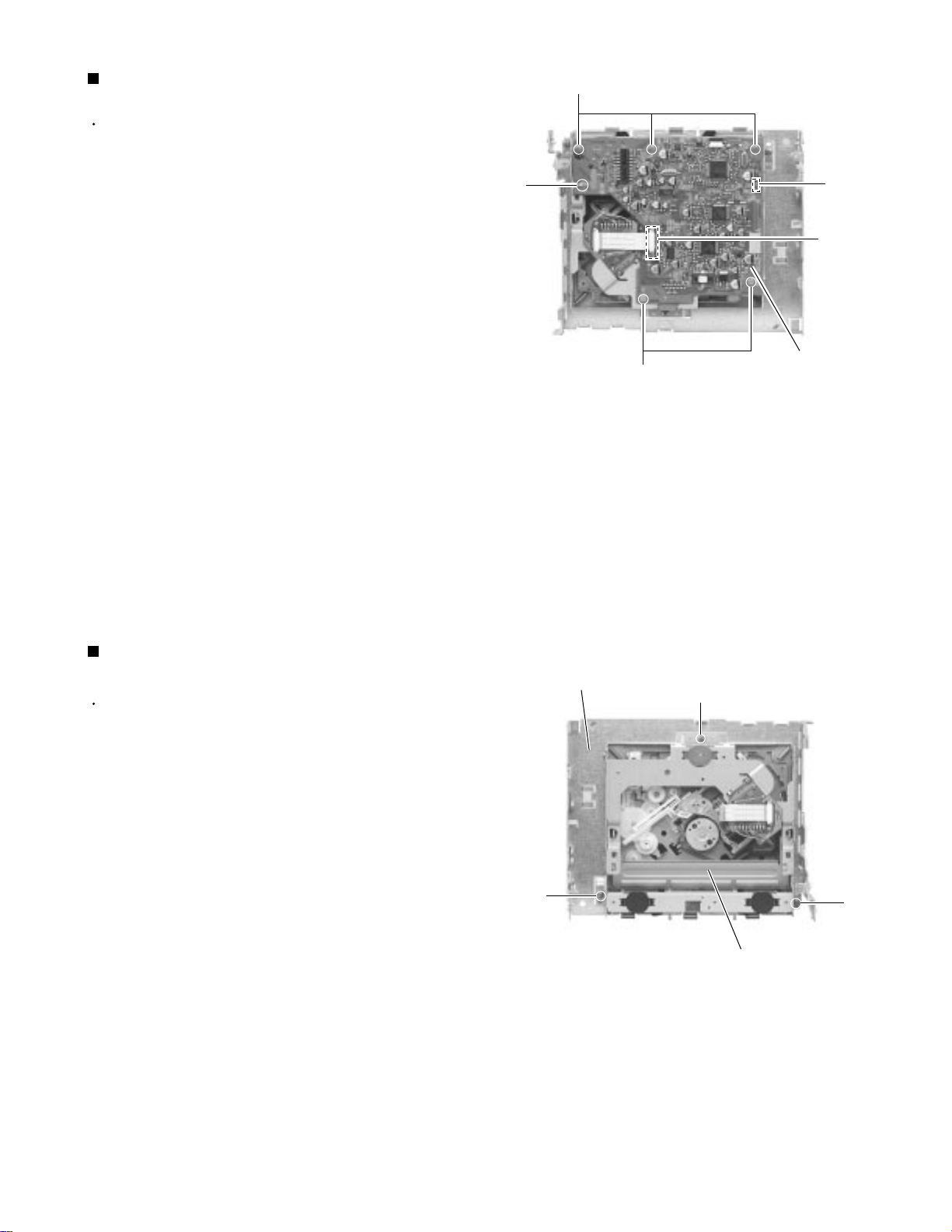
MN102H60KCC (IC801) : CPU
1.
Pin
layout
75 ~ 51
76
~
100
1 ~ 25
50
~
26
2. Pin function
Pin NO. Name Function
1
2
3
4
5
6
7
8
9
10
11
12
13~16
17
18
19
20
21
22
23
24
25
26~33
34
35~42
43
44
45
46
47
48
49
50
51
52
53
54
55
56
57
58
59
60
RES
RE
NC
NC
NC
CS0
SWLED7
SWLED4
SWLED5
SWLED6
NC
/WORD
A0~A3
VDD
NC
VSS
XI
XO
VDD
OSCI
OSCO
MODE
A4~A11
AVDD
A12~A19
AGND
ANA
Thermal
STOP
WDOUT
PON
RD
LCDCLK
WR
COLOR1
COLOR2
AVDD
RS
CS
COLOR3
VOL1
VOL2
SWLED3
I/O
LED reset input terminal
O
Redoinabl output terminal for enhancing memory
O
No connected
O
No connected
O
No connected
O
Chip selection 0 output terminal for enhancing memory
O
Output for SW_LED Flushing 7 (LED for cross key cover )
O
Output for SW_LED Flushing 4 (LED for [PRESET4-6] key)
O
Output for SW_LED Flushing 5 (LED for [SEEKUP]+[SEEKDOWN] key)
O
Output for SW_LED Flushing 6 (LED for [DISKUP]+[DISKDOWN] key)
O
No connected
O
Setting of width of bus of enhancing memory (H : 8bit)
I
Enhancing memory output terminal 0~3
O
Power supply terminal
Base clock output terminal
O
GND
Connects with GND
I
Opening
O
Power supply terminal
Crystal connection terminal (12.5MHz)
I
Crystal connection terminal (12.5MHz)
O
Mode set input terminal, pull-up (H : Memory extension mode)
I
Enhancing memory output terminal 4~11
O
Analog power supply terminal
Enhancing memory output terminal 12~19
O
Analog, standard power supply terminal, connects with GND
Audio level input for speana
I
Temperature fuse input
I
Stop state output terminal (At stop "H")
O
Watch dock timer overflow output terminal (At overflow "H")
O
Power supply on output terminal
O
LCD redostororb output terminal
O
LCD clock output for driver (180MHz)
O
LCD raitostororb output terminal
O
PWM output for color LED 1
O
PWM output for color LED 2
O
Analog, standard power supply terminal, connects with GND
LCD resist selection output terminal
O
LCD chip selection output terminal
O
PWM output for color LED 3
O
Rotary encoder input 1
I
Rotary encoder input 2
I
Output for SW_LED Flushing 3 (LED for [PRESET1-3] key)
O
1-36
Page 37

KD-LH2000R
Pin NO. Name Function
61
62
63
64
65
66
67
68
69
70
71
72
73
74
75
76
77
78
79
80
81
82
83
84~91
92
93~100
AGND
KEYO
KEY1
KEY2
KEY3
VDD
SWLED0
SWLED1
SWLED2
DISPCLK
DISPDATA
KEYDATA
SIFDA
SIFCK
GND
DISPCE
GND
PSAVE2
REMOTE
KEY_IN
ADSEP
RST
VDD
D0~D7
VSS
LCDDB0~LCDDB7
I/O
Analog terminal GND
KEY0 input AD terminal
I
KEY1 input AD terminal
I
KEY2 input AD terminal
I
KEY3 input AD terminal
I
Output for SW_LED Flushing 0 (LED for [VOL] key)
O
Output for SW_LED Flushing 1 (LED for [MODE]+[DISP]+[EQ] key)
O
Output for SW_LED Flushing 2 (LED for [CD / CD-CH]+[FM / AM] key)
O
Clock input for serial communications
I
Display data input (Cereal)
I
Key code data output (Cereal)
O
Onboard cereal writing data I/O terminal, Pull-up
I/O
Onboard cereal writing clock input terminal, Pull-up
I
I
Tippinabl input for serial communications
I
O
POWER SAVE 2 (Memory power supply OFF) detection input
I
Remote control input by codes terminal
I
Key interrupt input
I
Address data separation / common mode set terminal (H : Separation mode)
I
Reset input terminal ("L" resets by the input)
I
Power supply terminal
Enhancing memory input terminal 0~7
I
GND
LCD data bus I/O terminal 0~7
I/O
BU4066BCFV (IC131) : Quad analog switch
1.Pin layout & Block diagram
VDD CONT1 CONT4 IN4 IN3OUT4 OUT3
14 13 12 11 810 9
1234 756
IN1 OUT1 OUT2 IN2 VssCONT2 CONT3
1-37
Page 38

KD-LH2000R
TA2157FN-X(IC601):RF amp
1.Terminal layout
2.Block diagram
24 ~ 13
1 ~ 12
13
14
15
16
17
18
19
20
21
10pF
20k
20k
40k30k
20k 20k
15k
50 A
12k
12k
BOTTOM
PEAK
20k
20k
20k
PEAK
1.3V
40k
40k
240k
15pF
240k
15pF
50k
2k
20k
50k
14k
K
1
15k
x0.5
x2
x0.5
x2
1k
2k
1.75k
10pF
12
11
10
9
8
7
6
5
4
1-38
22
23
24
PIN SEL
VCTRLPIN
VCC
HiZ
GND
3k
3k
(APC SW)
APC ON
APC ON
APC OFF
(LDO=H)
180k
40pF
TEB
(TE BAL)
-50%
0%
+50%
180k
40pF
60k
60k
94k
22k
94k
22k
RFGC
(AGC Gian)
+12dB
+6dB
0dB
3
2
1
TEB
(TE BAL)
Normal mode
(0dB)
Normal mode
(0dB)
CD-RW mode
(+12dB)
Page 39

3.Pin function
Pin No. Symbol I/O Function
1
VCC
2
FNI
3
FPI
4
TPI
5
TNI
6
MDI
7
LDO
8
SEL
-
3.3V power supply pin
I
Main-beam amp input pin
I
Main-beam amp input pin
I
Sub-beam amp input pin
I
Sub-beam amp input pin
I
Monitor photo diode amp input pin
O
Laser diode amp output pin
I
APC circuit ON/OFF control signal, laser diode (LDO) control signal input
or bottom/peak detection frequency change pin.
KD-LH2000R
TA2175FN-X
9
10
11
12
13
TEB
TEN
TEO
RFDC
GVSW
SEL
GND
Hiz
VCC
I
Tracking error balance adjustment signal input pin
Adjusts TE signal balance by eliminating carrier component from PWM
signal (3-state output,PWM carrier = 88.2kHz) output from TC94A14F/FA
TEBC pin using RC-LPF and inputting DC.
TEBC input voltage:GND~VCC
I
Tracking error signal generation amp negative-phase input pin
O
Tracking error signal generation amp output pin.
Combining TEO signal RFRP signal with TC94A14F/FA configures tracking
search system.
O
RF signal peak detection output pin
I
AGC/FE/TE amp gain change pin
GVSW Mode
GND
Hiz
VCC
APC
circuit
OFF Connected VCC through 1k resistor
ON
ON
Control signal output
Control signal output
CD-RW
Normal
LDO
14
15
16
17
18
19
20
21
22
23
24
VRO
FEO
FEN
RFRP
REIS
RFGO
RFGC
AGCIN
RFO
RFI
GND
O
Reference voltage (VRO) output pin
VRO=1/2VCC When VCC=3.3V
O
Focus error signal generation amp output pin
I
Focus error signal generation amp negative-phase input pin
O
Signal amp output pin for track count
Combining RFRP signal and TEO signal with TC94A14F/FA configures
tracking search system.
I
O
RF signal amplitude adjustment amp output pin
I
RF amplitude adjustment control signal input pin
Adjusts RF signal amplitude by eliminating carrier component from PWM
signal (3-state output,PWM carrier=88.2kHz)output fromTC94A14F/14FA
RFGC pin using RC-LPF and inputting DC.
RFGC input voltage:GND~VCC
I
RF signal amplitude adjustment amp input pin
O
RF signal generation amp output pin
I
RF signal generation amp input pin
-
GND pin
1-39
Page 40

KD-LH2000R
TA8273H(IC951):Power AMP
1.Block diagram
INRF
0.22 F
AC CONT1
INRR
0.22 F
+
Vcc 1/2 Vcc 3/4
2200 F 0.022 F
6 20
+
11
-
+
+
-
9
7
OUT RF+
OUT RF-
1
Protective
circuit
+
-
+
12
+
-
GND
8
OUTRR+
5
OUTRR-
3
GND
2
ST BY
REF
47 F
INLF
AC CONT2
PRE GND
INLR
+5V
ST ON
+
0.22 F
+
0.22 F
4
Stand by
Switch
Mute
10
+
Ripple
Filter
Mute
22
circuit
3.3 F
+
15
-
+
-
17
19
10K
+
OUTLF+
OUTLF-
Low Level
Mute ON
25
18
21
23
GND
OUTLR+
OUT LR-
13
14
Protective
circuit
-
+
+
-
1-40
ON TIME
22 F
Muting &
16
+
ON Time Control
Circuit
GND
24
Page 41

2.Terminal layout
GND
GND
OUT1-
STBY
OUT1+
VP1
OUT2-
GND
OUT2+
SVRR
IN2
IN1
SGND
IN4
IN3
AC-GND
OUT3+
GND
OUT3-
VP2
OUT4+
MUTE
OUT4-
GND
KD-LH2000R
HSO
3.Pin function
1
2
3
4
5
6
7
8
9
10
11
12
13
14
15
16
17
18
19
20
21
22
23
24
25
SymbolPin No. Function
GND
GND
OUT1STBY
OUT1+
VP1
OUT2GND
OUT2+
SVRR
IN2
IN1
SGND
IN4
IN3
AUX
OUT3+
GND
OUT3VP2
OUT4+
MUTE
OUT4GND
HSO
Header of IC
Power GND
Outpur(-) for Rear Rch
Stand by input
Output (+) for Rear Rch
Power input
Output (-) for Front Rch
Power GND
Output (+) for Front Rch
Ripple filter
Front Rch input
Rear Rch input
Signal GND
Rear Lch input
Front Lch input
Power on time control
Output (+) for Front Lch
Power GND
Output (-) for Front Lch
Power input
Output (+) for Rear Lch
Muting control input
Output (-) for Rear Lch
Power GND
Header of IC
TA8273H
1-41
Page 42

KD-LH2000R
TC94A14FA (IC621) : D.SURVO & DSP
1.Terminal layout & block diagram
49
50
51
52
53
54
55
56
57
58
59
60
61
62
63
48 47 46 45 44 43 42 41 40 39
Clock
generator
Micro-
controller
interface
1-bit
DAC
Audio out
circuit
Address
circuit
circuit
Correction
Digital
output
16 k
RAM
PWM
Servo
control
ROM
RAM
CLV servo
Synchronous
guarantee
EFM
decoder
Sub code
decoder
38 37 36 35 34 33
D/A
A/D
Digital equalizer
automatic
adjustment circuit
Data
slicer
VCO
PLL
TMAX
32
31
30
29
28
27
26
25
24
23
22
21
20
19
18
64
2.Pin function
Pin
Symbol I/O Description
No
1
BCK
2
LRCK
O
Bit clock output pin.32fs,48fs,or 64fs selectable by command.
O
L/R channel clock output pin."L" for L channel and "H" for R channel. Output polarity
can be inverted by command.
3
AOUT
4
DOUT
5
IPF
O
Audio data output pin. MSB-first or LSB-first selectable by command.
O
Digital data output pin.Outputs up to double-speed playback.
O
Correction flag output pin. When set to "H", AOUT output cannot be corrected by C2
correction processing.
6
7
8
9
10
11
12
13
14
15
V
DD3
V
SS3
SBOK
CLCK
DATA
SFSY
SBSY
HSO
UHSO
PV
DD3
-
Digital 3.3V power supply voltage pin.
-
Digital GND pin.
O
Sub code Q data CRCC result output pin. "H" level when result is OK.
O
Sub code P-W data read I/O pin. I/O polarity selectable by command.
O
Sub code P-W data output pin.
O
Playback frame sync signal output pin.
O
Sub code block sync signal output pin. "H" level at S1 when sub code sync is detected.
I/O
General-purpose input / output pins.
Input port at reset.
-
PLL-only 3.3V power supply voltage pin.
17
161514131211101 2 3 4 5 6 7 8 9
1-42
Page 43

Pin
Symbol I/O Description
No
16
17
PDO
TMAX
EFM and PLCK phase difference signal output pin.
O
TMAX detection result output pin.
O
KD-LH2000R
TC94A14FA
18
19
20
21
22
23
24
25
26
27
28
29
30
31
32
33
34
35
36
37
38
39
40
41
42
43
44
45
46
47
48
49
50
51
52
53
54
55
56
57
58
59
60
61
62
63
64
LPFN
LPFO
PVREF
VCOF
AVSS3
SLCO
RFI
AVDD3
RFCT
RFZI
RFRP
FEI
SBAD
TEI
TEZI
FOO
TRO
VREF
RFGC
TEBC
SEL
AVDD3
FMO
DMO
VSS3
VDD3
TESIN
XVSS3
XI
XO
XVDD3
DVSS3R
RO
DVDD3
DVR
LO
DVSS3L
ZDET
VSS5
BUS0
BUS1
BUS2
BUS3
BUCK
/CCE
/RST
VDD5
TMAX Detection Result
Longer than fixed period
Within fixed period
Shorter than fixed period
Inverted input pin for PLL LPF amp.
I
Output pin for PLL LPF amp.
O
PLL-only VREF pin.
VCO filter pin.
O
Analog GND pin.
DAC output pin for data slice level generation.
O
RF signal input pin. Zin selectable by command.
I
Analog 3.3V power supply voltage pin.
RFRP signal center level input pin.
I
RFRP signal zero-cross input pin.
I
RF ripple signal input pin.
I
Focus error signal input pin.
I
Sub-beam adder signal input pin.
I
Tracking error input pin. Inputs when tracking servo is on.
I
Tracking error signal zero-cross input pin.
I
Focus equalizer output pin.
O
Tracking equalizer output pin.
O
Analog reference power supply voltage pin.
RF amplitude adjustment control signal output pin.
O
Tracking balance control signal output pin.
O
APC circuit ON/OFF signal output pin. At laser on, high impedance with UHS="L",
O
TMAX Output
DD3
"PV
"
"HiZ"
"AV
SS3
"
H output with UHS="H".
Analog 3.3V power supply voltage pin.
Feed equalizer output pin.
O
Disc equalizer output pin.
O
Digital GND pin.
Digital 3.3V power supply voltage pin.
Test input pin. Normally, fixed to "L".
I
System clock oscillator GND pin.
System clock oscillator input pin.
I
System clock oscillator output pin.
O
System clock oscillator 3.3V power supply voltage pin.
DA converter GND pin.
R-channel data forward output pin.
O
DA converter 3.3V power supply pin.
Reference voltage pin.
L-channel data forward output pin.
O
DA converter GND pin.
1 bit DA converter zero detection flag output pin.
O
Microcontroller interface GND pin.
Microcontroller interface data I/O pins.
I/O
Microcontroller interface clock input pin.
I
Microcontroller interface chip enable signal input pin.At "L", BUS0 to BUS3 are active.
I
Reset signal input pin. At reset, "L".
I
Microcontroller interface 5V power supply pin.
-
1-43
Page 44

KD-LH2000R
TC94A02F-005 (IC652) : MP3 DEC
AD11
AD12
32
31
33
AD10
CKS
30
TESTP
29
VSSR
28
VRAR
27
RO
26
VDAR
25
24
VDAL
LO
23
VRAL
22
VSSL
21
VSS
20
STANDBY
19
VDD
18
/OE
17
16
/CE
AD9
VDDT
AD8
AD7
AD6
REQ
VSS
AD13
DAC
34
Bus
register
C-Pointer
register
Y-Pointer
register
X-Pointer
Switch
register
35
36
37
General
Output Port
38
39
40
41
Flag
2sets
Address Calc.
ERAM
2k word
*3
CROM
4k word
DAC
AY
AX
MX MY MZ
X0 X1 X2
Y0 Y1 Y2
MAC ALU
A3
A2
A0 A1
round & limit
round & limit
Audio.I/F
15
AD5
14
LRCKI
13
BCKI
12
SDI
AD4
11
AD3
10
9
SDo
87
VDDT
AD14
/WR
AD16
AD15
IO0
IO1
VSS
VSSX
AD2
6
/MICK
543
MIDIo
AD1
AD0
MIMD
2
/RESET
1
42
YRAM
4k word
43
Timer
44
4546
47
48
Interrupt
Control
SRAM I/F
49
IO2
I-Bus
Generator
50
IO3
Timing
51
IO4
XRAM
4k word
52
VDD
53
IO5
X-Bus
Start
Prog.
54
IO6
Y-Bus
DIT
55
IO7
56
VSSP
PRAM
256word
57
PDO
Control
Program
PROM
4k*2+2k
VC0
58
VCOI
=10kword
59
VDDP
40bit
Decoder
Instruction
General Input Port
60
61
CK0
VDDX
Microcom.I/F
62
63
XI
64
XO
1-44
Page 45

KD-LH2000R
3.Pin function(1/2)
Pin No. Symbol
1
/RESET
2
3
4
5
6
7
8
9
10
11
12
13
14
15
16
17
18
19
20
21
22
23
24
25
26
27
28
29
30
31
32
33
34
35
36
37
38
39
40
41
42
43
44
45
46
47
48
49
50
MIMD
AD0
AD1
MIDIO
/MICK
AD2
VDDT
SDO
AD3
AD4
SDI
BCKI
LRCKI
AD5
CE
OE
VDD
STANBY
VSS
VSSL
VRAL
LO
VDAL
VDAR
RO
VRAR
VSSR
TESTP
CKS
AD12
AD11
AD10
AD9
VDDT
AD8
AD7
AD6
REQ
VSS
AD13
AD14
WR
AD16
AD15
IO0
IO1
VSS
IO2
IO3
I/O
O
O
I/O
O
O
O
O
O
O
O
O
O
O
O
O
O
O
O
O
O
O
O
O
O
O
I/O
I/O
I/O
I/O
Function
Hard reset input terminal(H:Normal operation L: Reset)
I
Micon I/F mode select input terminal
I
External SRAM address output 0 terminal
External SRAM address output 1 terminal
Micon I/F data input/output terminal
Micon I/F clock input terminal
I
External SRAM address output 2 terminal
Digital power supply (3.3V)
Data output terminal
External SRAM address output 3 terminal
External SRAM address output 4 terminal
Data input terminal 0
I
Bit clock input terminal A
I
LR clock input terminal A
I
External SRAM address output 5 terminal
External SRAM chip enable terminal
External SRAM output enable terminal
Digital power supply (2.5V)
Standby mode control terminal
I
Digital GND
DAC Lch GND
DAC Lch reference voltage terminal
DAC Lch output terminal
DAC Rch power supply terminal(2.5V)
DAC Lch power supply terminal(2.5V)
DAC Rch output terminal
DAC Rch reference voltage terminal
DAC Rch GND
Test terminal
I
VCO select terminal
I
External SRAM address output 12 terminal
External SRAM address output 11 terminal
External SRAM address output 10 terminal
External SRAM address output 9 terminal
Digital power supply terminal (3.3V)
External SRAM address output 8 terminal
External SRAM address output 7 terminal
External SRAM address output 6 terminal
Squeeze request terminal to host
Digital GND
External SRAM address output 13 terminal
External SRAM address output 14 terminal
External SRAM write signal
External SRAM address output 16 terminal
External SRAM address output 15 terminal
External SRAM data input/output 0 terminal
External SRAM data input/output 1 terminal
Digital GND
External SRAM data input/output 2 terminal
External SRAM data input/output 3 terminal
TC94A02F-005
1-45
Page 46

KD-LH2000R
3.Pin function(2/2)
Pin No. Symbol
51
52
53
54
55
56
57
58
59
60
61
62
63
64
IO4
VDD
IO5
IO6
IO7
VSSP
PDO
VCOI
VDDP
CKO
VDDX
XI
XO
VSSX
I/O
I/O
I/O
I/O
I/O
O
O
O
Function
External SRAM data input/output 4 terminal
Digital power supply (2.5V) terminal
External SRAM data input/output 5 terminal
External SRAM data input/output 6 terminal
External SRAM data input/output 7 terminal
VCO GND
PLL phase error detection signal output terminal
VCO control voltage input terminal
I
VCO power supply
-
16.934 MHz clock output terminal
Power supply (2.5V) terminal for oscillator
Connection terminal for oscillator(input)
I
Connection terminal for oscillator(output)
GND for oscillator
-
TC94A02F-005
LP61L1024S-12-X (IC653) : SRAM
1. Pin layout
V
NC
A16
A14
A12
I/O1
I/O2
I/O3
Vss
1
2
3
4
5
A7
6
A6
7
A5
8
A4
9
A3
10
A2
11
A1
12
A0
13
14
15
16
32
31
30
29
28
27
26
25
24
23
22
21
20
19
18
17
DD
A15
CS2
WE
A13
A8
A9
A11
OE
A10
CS1
I/O8
I/O7
I/O6
I/O5
I/O4
2. Block diagram
V
DD
Vss
A0
DECODER
A16
CS2
CS1
CONTROL
OE
WE
3. Pin function
SYMBOL
A0 - A16
I/O1 - I/O8
CS1, CS2
WE
OE
V
DD
Vss
NC
CORE
ARRAY
DATA I/O
I/O1
I/O8
DESCRIPTION
Address Input
Data Input/Output
Chip Select Inputs
Write Enable Input
Output Enable Input
Power Supply
Ground
No Connection
1-46
Page 47

MX23L8103-90 (IC802) : ROM
1.
Pin
layout
48
A15
A14
A13
A12
A11
A10
WE
RESET
RY/BY
A18
A17
NC
NC
NC
NC
1
2
3
4
5
6
7
A9
8
A8
9
10
11
12
13
14
15
16
17
18
A7
19
A6
20
A5
21
A4
22
A3
23
A2
24
A1
A16
47
BYTE
46
GND
45
Q15/A-1
44
Q7
43
Q14
42
Q6
41
Q13
40
Q5
39
Q12
38
Q4
37
VCC
36
Q11
35
Q3
34
Q10
33
Q2
32
Q9
31
Q1
30
Q8
29
Q0
28
OE
27
GND
26
CE
A0
25
2. Block diagram
CE
OE
WE
RESET
A0-A18
CONTROL
INPUT
LOGIC
ADDRESS
LATCH
AND
BUFFER
PROGRAM/ERASE
HIGH VOLTAGE
X-DECODER
MX29LV800T/B
FLASH
ARRAY
Y-DECODER
Y-PASS GATE
SENSE
AMPLIFIER
SOURCE
PGM
DATA
HV
ARRAY
HV
KD-LH2000R
WRITE
STATE
MACHINE
(WSM)
STATE
REGISTER
COMMAND
DATA
DECODER
COMMAND
DATA LATCH
3. Pin function
Pin NO. Name Function
1~8
9, 10
13, 14
16, 17
18~25
11
12
15
26
27
28
29
30
31
32
33
A15~A8
NC
WE
RESET
NC
RY / BY
A18, A17
A7~A0
CE
GND
OE
Q0
Q8
Q1
Q9
Q2
Address input
Write enable input
Hardware reset pin
Ready / busy output
Address input
Address input
Chip enable input
Ground pin
Output enable input
Data input / output
Data input / output
Data input / output
Data input / output
Data input / output
PROGRAM
DATA LATCH
Q0-Q15/A-1
I/O BUFFER
Pin NO. Name Function
34
35
36
37
38
39
40
41
42
43
44
45
46
47
48
Q10
Q3
Q11
VCC
Q4
Q12
Q5
Q13
Q6
Q14
Q7
Q15 / A-1
GND
BYTE
A16
Data input / output
Data input / output
Data input / output
Data input / output
Data input / output
Data input / output
Data input / output
Data input / output
Data input / output
Data input / output
Data input / output
Q15 (Word mode) /
LSB addr (Byte mode)
Ground pin
Word / byte selction input
Address input
1-47
Page 48

KD-LH2000R
PCM1716E (IC571) : D/A converter
1. Pin layout
2. Block diagram
BCK
LBCK
DATA
ML/llS
MC/DM1
MD/DM0
CS/WO
MODE
MUTE
RST
3. Pin function
Pin
Symbol Function
No.
1
LRCK
2
DATA
3
BCK
4
CLKO
5
6
7
8
9
10
11
12
13
14
15
16
17
18
19
20
21
22
23
24
25
26
27
28
XTI
XTO
DGND
VDD
VDD2R
AGND2R
EXTR
NC
VOUTR
AGND1
Vcc1
VOUTL
NC
EXTL
AGND2L
Vcc2L
ZERO
RST
CS/IWO
MODE
MUTE
MD/DM0
MC/DM1
ML/IIS
28 15
114
Serial
Input
I/F
Mode
Control
I/F
Mult-level
8X Oversampling
Digital Filter
with
Function Controller
SCK
BPZ-Cont
Crystal OSC
XTI XTO CLKO Vcc1 VccAGND1 DGND
Delta-Sigma
Modulator
Power Supply
Vcc2L
DAC
DAC
AGND2L
Vcc2R
AGND2R
Open drain
Low-pass
Filter
Low-pass
Filter
I/O
I
LRCK clock input
I
Serial audio data input
I
Bit clock input for serial audio data
O
Buffered output of system clock
I
Oscillator input / External clock input
O
Oscillator output
-
Digital ground
-
Digital power +5V
-
Analog power +5V
-
Analog ground
O
Rch common pin of analog output amp
-
Non connection
O
Rch analog voltage output of audio signal
-
Analog ground
-
Analog power +5V
O
Lch analog voltage output of audio signal
-
Non connection
O
Lch common pin of analog output amp
-
Analog ground
-
Analog power +5V
O
Zero data flag
I
Reset
I
Chip select / Input format selection
I
Mode control select
I
Mute control
I
Mode control, Data / De-emphasis selection 1
I
Mode control, BCK / De-emphasis selection 2
I
Mode control, WDCK / Input format selection
VoutL
EXTL
VoutR
EXTR
ZERO
1-48
Page 49

NJM2360M (IC921) : DC-DC convertor
1.
Pin
layout
2. Block diagram
KD-LH2000R
1. Cs
1
2
3
4
8
7
6
5
2. Es
T
3. C
4. GND
5. INV
6. Vcc
7. S
I
8. C
D
IN
HN58X2432FPI (IC703) : EEPROM
1.Terminal layout
Switch
collector
Switch
emitter
Timing
capacitor
GND
2.Pin function
1
Q
1
QS
Q
2
R
2
Ipk
COSC
T
3
COMP
V
REF
4
1.25V
+
-
Driver
8
collector
Ipk sense
7
+
6
V
Comparator
5
reversal input
A0
A1
A2
GND
1
2
3
4
3.Block diagram
A0, A1, A2
V
CC
V
SS
WP
SCL
SDA
8
VDD
7
WPIN
6
SCL
SDA
5
Control
logic
Pin name
A0 to A2
SCL Serial clock
SDA Serial data
WPIN
VDD
CND
Address generator
Device address
Write protect
Power supply
Ground
High voltage generator
X decoderY decoder
Y-serect & Sense amp.
Function
input
input/output
Memory array
Serial-parallel converter
1-49
Page 50

KD-LH2000R
SAA6579T-X(IC51):RDS detecter
1.Pin layout
QUAL
SCOUT
2.Block diagram
DATA
Vref
MUX
GND
CIN
1
2
3
4
dd
V
5
6
7
8
16
15
14
13
12
11
10
CLK
T57
OSCO
OSCI
V
dd
GND
TEST
MODE
9
121413
3.Pin function
4
8
7
CLOCKED
COMPARATOR
5
3
REFERENCE
VOLT AGE
Pin No.
1
2
3
4
ANTIALIASING
FILTER
6 11
Symbol
VP1
QUAL
DATA
Vref
MUX
57 kHz
BAND PASS
(8th ORDER)
COSTAS LOOP
VARIABLE AND
FIXED DIVIDER
CLOCK
REGERATION
AND SYNC
RECONSTRUCTION
FILTER
TEST LOGIC AND OUTPUT
SELECTOR SWITCH
OSCILLATOR
AND
DIVIDER
BIPHASE
SYMBOL
DECODER
910
Description
Quality indication output
RDS data output
Reference voltage output (0.5VDDA)
Multiolex signal input
QUALITY BIT
GENERATOR
DIFFERENTIAL
DECODER
1
2
15
15
1-50
5
6
7
8
9
10
11
12
13
14
15
16
Vdd
GND
CIN
SCOUT
MODE
TEST
GND
Vdd
OSCI
OSCO
T57
CLK
+5V supply voltage for analog part
Ground for analog part (0V)
Sub carrier input to comparator
Sub carrier output of reconstruction filter
Oscillator mode / test control input
Test enable input
Ground for digital part (0V)
+5V supply voltage for digital part
Oscillator input
Oscillator output
57 kHz clock signal output
RDS clock output
Page 51

RPM6938-SV4 (IC805) : Remote sensor
1.Block diagram
KD-LH2000R
AGC
AMP
I/V
conversion
PD
magnetic shield
BPF
fo
trimming
circuit
Detector
NJU7241F25 (IC651) : Regulator
1.Pin layout 2.Block diagram
GND 1
VIN 2
5 STB
VIN 2
Vcc
Comp
Vcc
22k
Rout
GND
Short protect
3 VOUT
VOUT 3
4 NC
STB 5
GND 1
NJM4565V (IC132,IC151,IC251,IC572) : Dual ope amp
1.Terminal layout & Pin function
1
1
8
A
2
+
-
7
B
3
+
-
4
6
5
AOUTPUT
2
A-INPUT
3
A+INPUT
4
V
5
B+INPUT
6
B-INPUT
7
B OUTPUT
8
V
Vref
1 GND
1-51
Page 52

KD-LH2000R
VICTOR COMPANY OF JAPAN, LIMITED
MOBILE ELECTRONICS DIVISION
PERSONAL & MOBILE NETWORK BUSINESS UNIT. 10-1,1Chome,Ohwatari-machi,Maebashi-city,371-8543,Japan
(No.49753)
200206
 Loading...