

Page 1
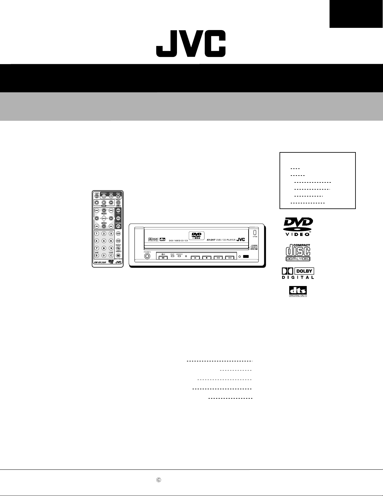
SERVICE MANUAL
DVD/CD PLAYER
KV-DV7
KV-DV7
E
J
UF
UT
US
A
Area Suffix
Continental Europe
Northern America
China
Taiwan
Singapore
Australia
Contents
Safety precaution
Important for laser products
Disassembly method
Adjustment method
Description of major ICs
COPYRIGHT 2001 VICTOR COMPANY OF JAPAN, LTD.
1-2
1-3
1-4
1-11
1-12~17
No.49630
Apr. 2001
Page 2
KV-DV7
Safety precaution
!
!
Burrs formed during molding may be left over on some parts of the chassis. Therefore,
pay attention to such burrs in the case of preforming repair of this system.
Please use enough caution not to see the beam directly or touch it in case of an
adjustment or operation check.
1-2
Page 3
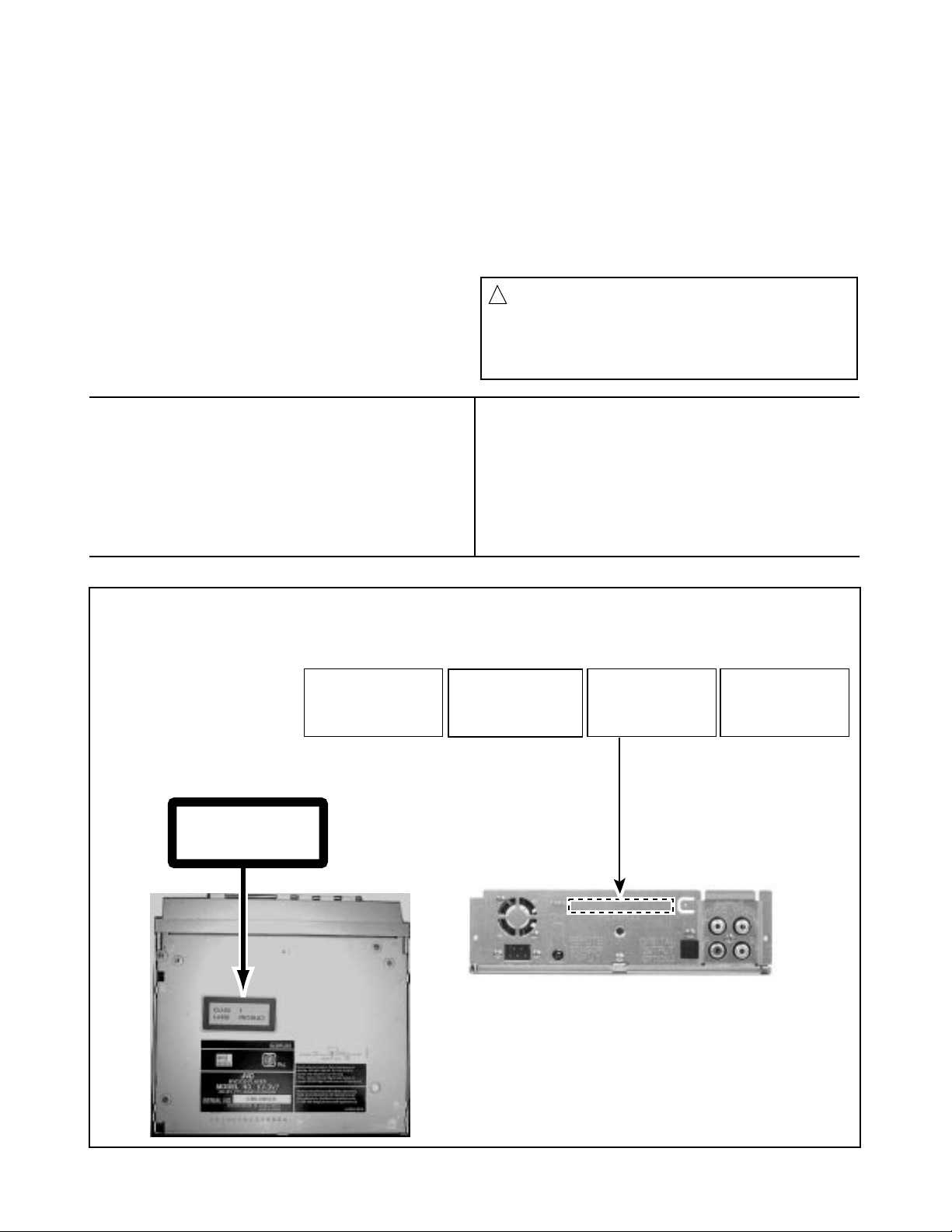
Important for laser products
KV-DV7
1.CLASS 1 LASER PRODUCT
2.DANGER : Invisible laser radiation when open and inter
lock failed or defeated. Avoid direct exposure to beam.
3.CAUTION : There are no serviceable parts inside the
Laser Unit. Do not disassemble the Laser Unit. Replace
the complete Laser Unit if it malfunctions.
4.CAUTION : The compact disc player uses invisible
laserradiation and is equipped with safety switches
whichprevent emission of radiation when the drawer is
open and the safety interlocks have failed or are de
feated. It is dangerous to defeat the safety switches.
VARNING : Osynlig laserstrålning är denna del är öppnad
och spårren är urkopplad. Betrakta ej strålen.
VARO : Avattaessa ja suojalukitus ohitettaessa olet
alttiina näkymättömälle lasersäteilylle.Älä katso
säteeseen.
5.CAUTION : If safety switches malfunction, the laser is able
to function.
6.CAUTION : Use of controls, adjustments or performance of
procedures other than those specified herein may result in
hazardous radiation exposure.
CAUTION
!
Please use enough caution not to
see the beam directly or touch it
in case of an adjustment or operation
check.
ADVARSEL : Usynlig laserstråling ved åbning , når
sikkerhedsafbrydere er ude af funktion. Undgå
udsættelse for stråling.
ADVARSEL : Usynlig laserstråling ved åpning,når
sikkerhetsbryteren er avslott. unngå utsettelse
for stråling.
REPRODUCTION AND POSITION OF LABELS
WARNING LABEL
CLASS 1
LASER PRODUCT
DANGER : Invisibie laser radiation
when open and interlock or
defeated.
AVOID DIRECT EXPOSURE TO
BEAM (e)
VARO : Avattaessa ja suojalukitus
ohitettaessa olet alttiina
näkymättömälle lasersäteilylle.Älä
katso säteeseen. (d)
VARNING : Osynlig laserstrålning är
denna del är öppnad och spårren är
urkopplad. Betrakta ej strålen. (s)
ADVARSEL :Usynlig laserstråling
ved åbning , når
sikkerhedsafbrydere er ude af
funktion. Undgå udsættelse for
stråling. (f)
1-3
Page 4
KV-DV7
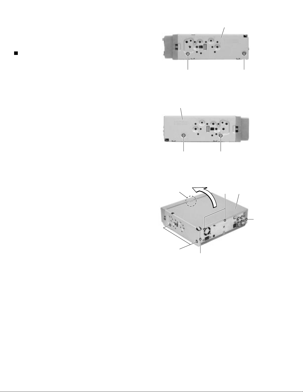
Disassembly method
< Main Body>
Removing the top cover (See Fig.1 to 3)
1.
Remove the seven screws A on both sides and
back of the body.
2.
Detach the rear part of the top cover upward and
release the joint a on the top side.
Top cover
AA
Fig.1
Top cover
AA
Fig.2
Joint a
A
A
Fig.3
A
Top cover
A
1-4
Page 5
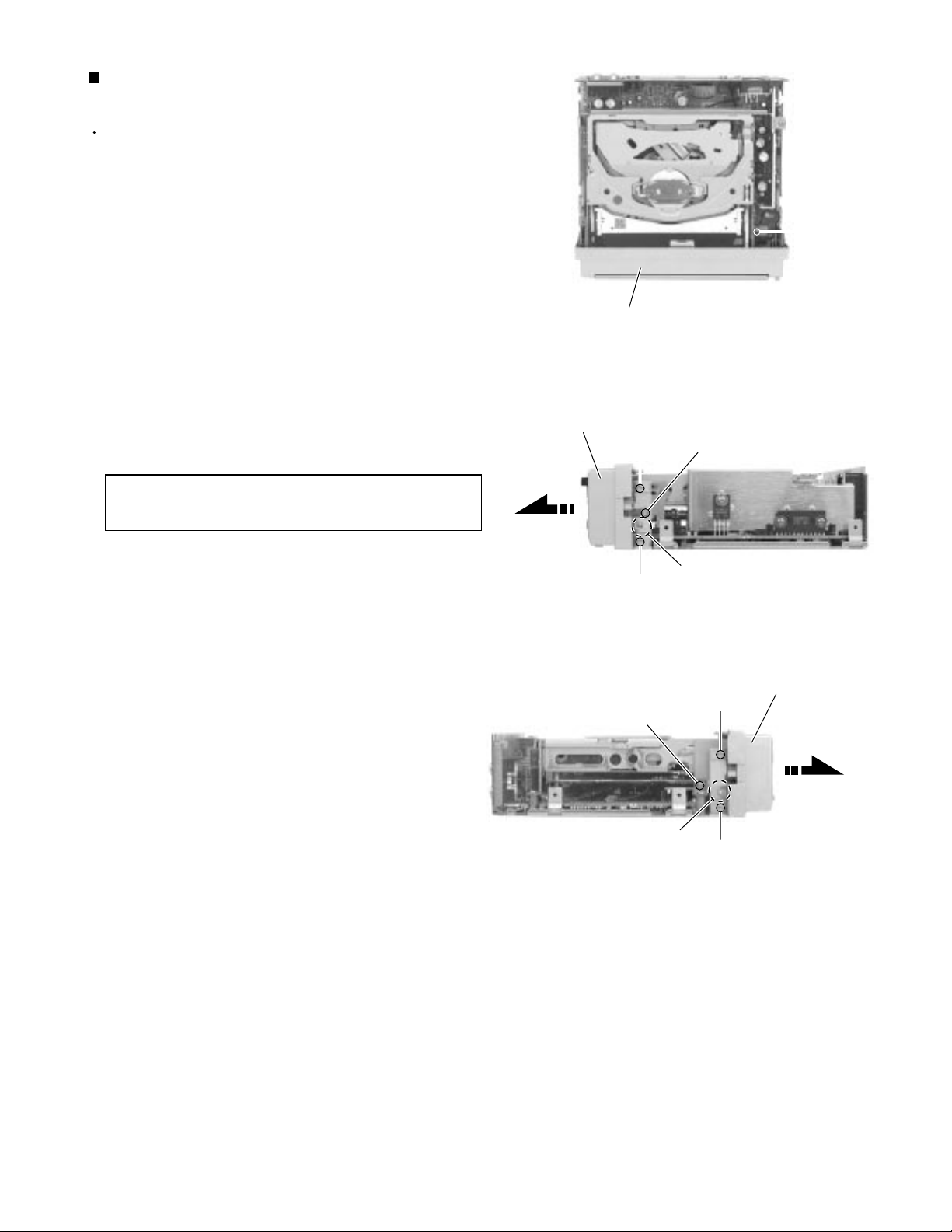
Removing the front panel assembly
(See Fig.4 to 6)
Prior to performing the following procedure, remove
the top cover.
1.
Remove the screw B attaching the ground on the
top of the body.
KV-DV7
2.
Remove the four screws C and two screws C'
attaching the front panel assembly on both sides of
the body.
3.
Release the two joints b of the front panel assembly
and the bottom chassis on both sides of the body
and remove the front panel assembly toward the
front.
The connector CN801 on the control switch board in
the front panel assembly will be disconnected from
the main board.
CAUTION:
When reassembling, attach the four
screws C and then the two screws C'.
Front panel assembly
Front panel assembly
C
C
C'
B
Fig.4
C'
Joint b
Fig.5
Front panel assembly
C
Joint b
Fig.6
C
1-5
Page 6
KV-DV7
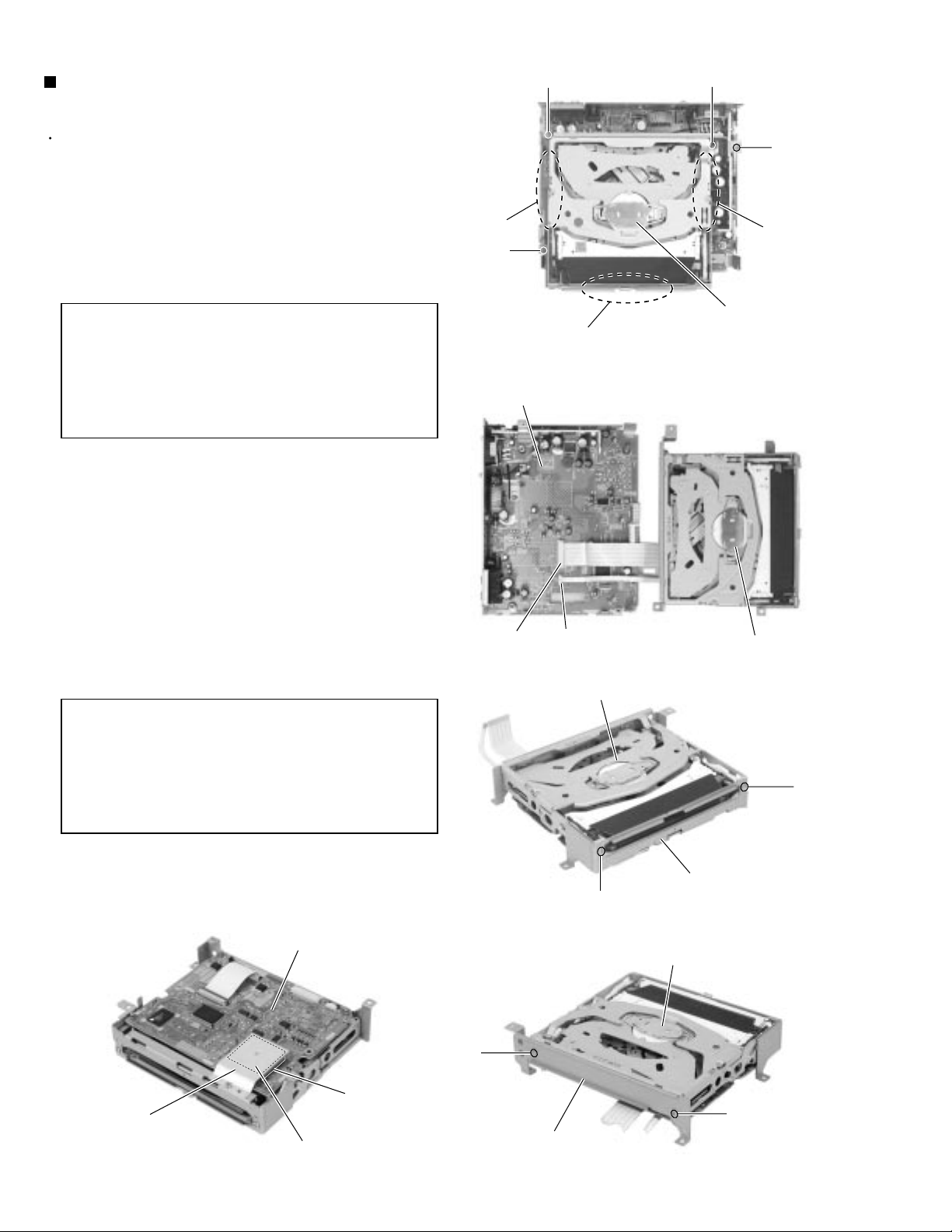
Removing the DVD mechanism
assembly (See Fig.7 to 11)
Prior to performing the following procedure, remove
the top cover and the front panel assembly.
1.
Remove the four screws D attaching the DVD
mechanism assembly on the top of the body.
2.
Remove the DVD mechanism assembly while
holding the part c on each side of the assembly.
CAUTION:
3.
Disconnect the card wire from connector CN721 and
CN701 on the main board andremove the DVD
mechanism assembly from the body.
To protect accuracy of the mechanism
bracket on the front of DVD mechanism
assembly, make sure to hold the part c
on each side of the DVD mechanism
assembly when removing or
reassembling.
Joint c
D
Do not hold the mechanism bracket.
Fig.7
Main board
DD
D
Joint c
DVD mechanism assembly
4.
Remove the two screws E attaching the DVD
mechanism bracket (1) on the front sideof the DVD
mechanism assembly.
5.
Remove the two screws F attaching the DVD
mechanism bracket (2) on the rear sideof the DVD
mechanism assembly.
CAUTION:
When reassembling the DVD
mechanism assembly, attach the cooling
rubber and the heat sink to the DVD
mechanism board as shown in Fig.11 to
make sure radiation of IC15 on the DVD
mechanism board (Fig.11).
DVD mechanism board
CN701
DVD mechanism assembly
CN721
E
DVD mechanism assembly
Fig.8
E
DVD mechanism bracket (1)
Fig.9
DVD mechanism assembly
1-6
Heat sink
IC15
Cooling rubber
F
F
DVD mechanism bracket (2)
Fig.10Fig.11
Page 7

KV-DV7
Removing the main board
(See Fig.12 to 15)
Prior to performing the following procedure, remove
the top cover, the front panel assembly and the DVD
mechanism assembly.
1.
Disconnect the wire from connector CN781 on the
main board.
2.
Remove the three screws G on the top of the body.
3.
Remove the screw H on the back of the body.
4.
Disengage the joint d in the lower right part of the
rear panel and remove the rear panel with the main
board (The fan assembly will be detached with the
rear panel).
CAUTION:
When reattaching, engage the joint c to
place the rear panel on the back of the
bottom chassis.
Main board
G
Rear panel
CN781
Bottom chassis
Fig.12
Rear panel
5.
Remove the two screws I and J attaching the main
board to the rear panel.
Rear panel
IJ
Fig.15
H
Fig.13
Main board
Rear panel
Joints d
Fig.14
1-7
Page 8

KV-DV7
Removing the fan assembly
(See Fig.16 and 17)
Prior to performing the following procedure, remove
the top cover, the front panel assembly and the DVD
mechanism assembly.
REFERENCE:
1.
Disconnect the wire from connector CN781 on the
main board.
2.
Remove the two screws K on the back of the body.
It is not unnecessary to remove the main
board and the rear panel.
Rear panel
K
Fan assembly
Fan assembly
CN781
Fig.16
Rear panel
Fig.17
Removing the control switch board
(See Fig.18)
Prior to performing the following procedure, remove
the top cover and the front panel assembly.
1.
Remove the three screws L attaching the control
switch board on the back of the front panel
assembly.
2.
Disengage the three joints e of the front panel and
the control switch board.
Joint d
L
Joint e
Front panel assembly
L
Control switch board
Fig.18
Joint e
L
1-8
Page 9

KV-DV7
Replacing the DVD door flame
(See Fig.19 to 24)
Prior to performing the following procedure, remove
the front panel assembly and the control switch
board.
1.
Remove each button on the back of the front panel.
2.
Press the OPEN button on the front side of the front
panel to open the DVD door.
3.
Remove the six screws M attaching the DVD door
flame on the back of the front panel.
4.
Disengage the three joints f on the top of the DVD
door flame using a screwdriver (-) to pull out the
three bosses of the front panel. Peel off the two
adhesive tapes at the same time.
5.
Detach the bottom of the DVD door flame. Press the
lock lever on the front side of the front panel and
remove the DVD door flame from the gear.
CAUTION:
When reassembling, reattach the DVD
door flame to the front panel with the
two adhesive tapes while engaging the
three joints f.
Eject button
M
Reset button
Front panel
DVD door flame
MM
Control button
Power button
Fig.19
OPEN button
DVD door
Fig.20
M
Detach the lock lever from the front side, then from the gear.
DVD door flame (remove from bottom)
DVD door flame
Fig.22
Front panel
Bosses
Joint f
Insert a screwdriver.
Joint f
Adhesive tapes
Fig.21
Lock lever
Joint f
DVD door flame
Adhesive tapes
DVD door flame
DVD door
Fig.23Fig.24
1-9
Page 10

KV-DV7
Removing the DVD door
(See Fig.25 to 29)
Prior to performing the following procedure, remove
the front panel assembly, the control switch board
and the DVD door flame.
1.
Remove the screw N attaching the gear assembly
on the back of the front panel.
2.
Pull out the DVD door shaft from the joint g of the
DVD door and the front panel.
3.
Remove the DVD door with the gear assembly.
4.
Remove the spring through the notch h of the gear
assembly bracket and remove the DVD door from
the gear assembly.
CAUTION:
CAUTION:
Do not lose the spring.
Reattaching the DVD door, reattach the
spring through the notch h and hole i of
the gear assembly bracket, then
reassemble the DVD door and the gear
assembly. Reattach them to the front
panel.
Gear assembly
N
DVD door (Shaft)
Gear assembly
Joint g
DVD door
Fig.25
Fig.26
DVD door
1-10
DVD door
Spring
Hole i
Shaft
Bracket
Gear assembly
Bracket
M
Fig.27
DVD door
Spring
Notch h
Fig.28Fig.29
Page 11

Adjustment method
This model dose not have adjustment.
If you change printed circuit board or mechanism assembly, please
check as folow as next.
Test instruments required for checking
(1) Digital oscilloscope (100MHz)
(2) AM standard signal generator
(3) FM standard signal generator
(4) Stereo modulator
(5) Electric voltmeter
(6) Digital tester
(7) Monitor
(8) Test disc : VT-501 for DVD section
: CTS-1000 for CD section
Checking items
KV-DV7
(1) DVD section: Playback the test disc VT-501.
It should not have some noise on the audio signal or video signal.
(2) CD section : Playbcak the test disc CTS-1000.
It should not heve some noise on the audio signal.
1-11
Page 12

KV-DV7
Description of major ICs
UPD780058GC-250 (IC701) : Micon
1. Pin layput
2. Pin function (1/2)
Pin No.
1
2
3
4
5
6
7
8
9
10
11
12
13
14
15
16
17
18
19
20
21
22
23
24
25
26
27
28
29
30
31
32
33
34
35
36
EEPROM_CONT
37
38
39
40
61 ~ 80
Symbol
TEMP
AVSS
LCDCONT
D_OUT_MUTE
AVREF1
LCDDI/RXDO
LCDDO/TXDO
LCDCL/ASCK
JBUS_SI
JBUS_SO
JBUS_SCK
JBUS_CTRL+B
ANT_FM
D_HOST
D_FM
SCK
RDY_FM
/HOST_RST
NTSC/PAL
E.VOL_SCK
E.VOL_DO
E.VOL_STB
V_MUTE
A_MUTE
D_MUTE
LED_DISCIN
LED_DSP
LED_CD/DVD
LED_DVD
EEPROM_DO
VSS1
EEPROM_DI
EEPROM_CLK
FANCONT
LCDCE
60 ~ 41
1 ~ 20
I/O
I
-
-
-
-
I
I
-
O
-
I
O
O
I
O
I
-
O
I
O
I
O
O
O
O
O
O
O
O
I
O
O
O
O
-
-
-
-
-
O
-
-
-
40 ~ 21
Function
Templature sensor
Non connect
Non connect
Audio ground
LCD control
DIgital out mute
Anarog reference voltage
Communication for JIG LCD or PC
Communication for JIG LCD or PC
Communication for JIG LCD or PC
J-BUS serial input
J-BUS serial output
J-BUS serial clock input
Power supply for J-BUS control
Communication for DVD mechanism
Communication for DVD mechanism
Communication for DVD mechanism
Communication for DVD mechanism
Communication for DVD mechanism
Communication for DVD mechanism
NTSC/PAL control (H:PAL L:NTSC)
E. volume serial clock output
E. volume data output
E. volume strobe output
Video mute output
Audio mute output
Audio mute input
LED output for slot
LED output for Real sonic or Remocon
LED output for CD/DVD
LED output for DVD
Non connect
Ground1
Non connect
Non connect
Non connect
Fan control
Non connect
Non connect
LCD chip select
1-12
Page 13

2. Pin function (2/2)
KV-DV7
Pin No.
41
42
43
44
45
46
47
48
49
50
51
52
53
54
55
56
57
58
59
60
61
62
63
64
65
66
67
68
69
70
71
72
73
74
75
76
77
78
79
80
Symbol
LCDRST
JBUS_I/O
S1_CONT
SIDE_BRAKE
HEADPHONE
REMOCON_SEL
SB_SEL_V
SB_SEL_OP
LCD/PC_SEL
ADDRESS_SEL
NTSC/PAL_SEL
VSYNC
POWER_CONT
+7V_CONT
+5V_CONT
LED_CONT
PLAY_REMOTE
LINE_IN
CD_DET
RESET
J-INT
P.SAVE2(BATT)
P.SAVE1(ACC)
FM_INT
REMOCON
KEY_INT
VSS0
VDD1
X2
X1
IC
XT2
XT1
VDD0
AVREF0
ANI0
ANI1
ANI2
ANI3
ANI4
I/O
-
I/O
I
I
I
I
I
I
I
I
O
O
O
O
O
I
I
O
I
I
I
I
I
I
-
O
O
I
I
I
I
I
Function
Non connect
J-BUS I/O
S1 control
Side brake detection
Headphone detection
Remocon code select
Side brake select
Side brake select
Communication select
Address select on J-BUS
NTSC/PAL select
Power supply control
Mechanism power supply +7V control
Mechanism power supply +5V control
Power supply control od LED & Remocon
Play remote output
LINE IN control
Non connect
Reset
J-BUS initialize
Battery detection
ACC detection
DVD mechanism communication
Remocon input
KEY_INT
Setting to input for common use
Power supply1
Connect to X'tal
Connect to X'tal
Non connect
Power supply
Power supply 0
Referencew voltage
Key input 0
Key input 1
Key input 2
Key input 3
Key input 4
1-13
Page 14

KV-DV7
BA4901A-V3 (IC911) : Regulator
1. Pin layout
2.Pin Function
123456789
9V
VCC-B
VCC-C
ACC5V
ACC.IN
CDBV
VDD5V
CTRL
MEMORY.IN
101112
AJ
10V
GND
Pin No. Symbol Descriptions
1
2
3
4
5
VCC-C
VCC-B
ACC5V
ACC.IN
VDD5V
To be connected with the collector of PNP.
To be connected with the base of PNP.
A voltage supply for ACC block.
Control of the COMP output by inputting voltage.
Output voltage level is 5.7V, and max output current is 100mA.
This voltage supply is for microcomputer. Whenever backup voltage
supply is connected, the output keeps on running.
6
9V
This output voltage is 9.0V, and max output current is 500mA.
This voltage supply for AUDIO.
7
CDBV
This output voltage is 8.0V, and max output current is 1A
This voltage supply for CD.
10
8
9
CTRL
MEMORY.IN
10V
Output selector of CD, AUDIO, ILM and Vcc-B.
To be connected with the BACKUP of car
This output voltage is 10V, and max output current is 500mA.
Output voltage is adjustable.
11
AJ
Putting a resistance between ILM and AJ or between AJ and GND males
ILM output voltage adjustable.
12
GND
Connect to GND
LM2596S-ADJ-W (IC951) : Regulator
1. Pin layout 2. Block diagram
CURRENT
SOURCE
BIAS
15
FEEDBACK
R1=2.5k
3.3V, R2 = 4.2k
5V, R2 = 7.5k
12V, R2 = 21.8k
ADJ, R2 = 0
R1 = OPEN
1-14
R2
1.235V
REFERENCE
ACTIVE
CAPACITOR
AMP
OP AMP
REGULATOR
GM
2.5V
2.5V
ON/OFF
START
UP
COMP.
FREQ. SHIFT
150kHz
OSC.
LATCH
CURRENT
LIMIT
RESET
220mV
COMP.
COMP.
DRIVER
THERMAL
LIMIT
200mV
3A
SWITCH
~
VIN
OUTPUT
GND
Page 15

IC-PST9333U-X (IC741) : Regulator
1. Pin layout
KV-DV7
2. Block diagram
NC 1
GND 2
4 Vcc
3 VOUT
Vcc 4
NC 1
3. Pin function
Pin No.
1
2
3
4
Symbol
NC
GND
VOUT
Vcc
Function
Non connect
GND terminal
Reset signal output terminal
Vcc terminal/Voltage detect terminal
NJM2267X-X (IC301) : Video amp.
1. Pin layout 2. Block diagram
3 VOUT
2 GND
V+
7
VIN1
GND
VSAG1
VOUT1
1
2
3
4
8
7
6
5
VIN2
V+
VSAG2
VOUT2
VIN 2
VIN 1
8
1
CLAMP CLAMP
20k
20k
6.2dB
Amp
6.2dB
Amp
2.2k
2.2k
75
DRIVER
75
DRIVER
SAG TERMINAL
SAG TERMINAL
2
GND
750
750
5
6
4
3
VOUT2
VSAG2
VOUT1
VSAG1
1-15
Page 16

KV-DV7
NJM4580V-X (IC101,IC151) : Ope amp.
1. Pin layout & Block diagram
A OUTPUT
1
8
A
A-INPUT
2
7
B
A+INPUT
V-
3
4
6
5
RPM6938-V4 (IC801) : Remocon reseiver
1. Block diagram
V+
B OUTPUT
B-INPUT
B+INPUT
PQ05RD21 (IC961) : Regulator
1. Block diagram
Vin 1
IC
3
GND
2 Vo
4 Vc
AMP
I/V
conversion
PD
magnetic shield
BPF Detector
for
trimming
circuit
TA78L05F-X (IC971) : Regulator
1. Pin layout
AGC
Vcc
22k
Comp
Vcc
ROUT
GND
TC7SET08F-X (IC511) : Regulator
2. Truth table1. Pin layout
45
123
A
B
Y
L
L
L
L
H
L
H
L
L
H
H
H
1-16
123
Page 17

TC9260F-X (IC131) : E. volume
1. Pin layout 2. Pin function
KV-DV7
1
Vss
2
OUT
3
IN
4
LD1
5
LD2
CS
CK
6
7
8
A-GND
3. Block diagram
OUT 2
16
15
14
13
12
11
10
9
VDD
OUT
IN
LD1
LD2
A-GND
STB
DATA
Vss
1
Pin No.
1
2
3
4
5
6
7
8
9
10
11
12
13
14
15
16
VDD
16
Symbol
Vss
L-OUT
L-IN
L-LD1
L-LD2
L-GND
CS
CK
DATA
STB
R-GND
R-LD2
R-LD1
R-IN
R-OUT
VDD
Function
Digital ground terminal
Volume output terminal
Volume input terminal
Tap out terminal for loudness(1)
Tap out terminal for loudness(2)
Analog ground terminal
Chip select terminal
Clock input terminal
Data input terminal
Strobe input terminal
Analog ground terminal
Tap output terminal for loudness(2)
Tap output terminal for loudness(1)
Volume input terminal
Volume output terminal
Power supply terminal
15 OUT
L-ch
VOLUME
IN 3
LD1 4
LD2 5
A-GND 6
CS 7
CK 8
L-ch
LATCH
DATA DECODER STB GENERATOR
SHIFT REGISTER (13bit)
R-ch
LATCH
14 IN
13 LD1
12 LD2
11 A-GND
10 STB
9 DATA
R-ch
VOLUME
1-17
Page 18

KV-DV7
VICTOR COMPANY OF JAPAN, LIMITED
MOBILE ELECTRONICS DIVISION
PERSONAL & MOBILE NETWORK BUSINESS UNIT. 10-1,1Chome,Ohwatari-machi,Maebashi-city,371-8543,Japan
(No.49630)
200104
 Loading...