


ISSI IS61VPD51236-200TQI, IS61VPD51236-200TQ, IS61VPD51236-166TQI, IS61VPD51236-166TQ, IS61VPD51236-166BI Datasheet
...IS61VPD51232
IS61VPD51236 ISSI®
IS61VPD10018
512K x 32, 512K x 36, 1024K x 18 SYNCHRONOUS PIPELINED,
DOUBLE CYCLE DESELECT STATIC RAM
ADVANCE INFORMATION
MAY 2001
FEATURES
•Internal self-timed write cycle
•Individual Byte Write Control and Global Write
•Clock controlled, registered address, data and control
•Linear burst sequence control using MODE input
•Three chip enable option for simple depth expansion and address pipelining
•Common data inputs and data outputs
•JEDEC 100-Pin TQFP and 119-pin PBGA package
•Single +2.5V, ±5% operation
•Auto Power-down during deselect
•Double cycle deselect
•Snooze MODE for reduced-power standby
•JTAG Boundary Scan for PBGA package
FAST ACCESS TIME
DESCRIPTION
The ISSI IS61VPD51232, IS61VPD51236, and IS61VPD10018 are high-speed, low-power synchronous static RAMs designed to provide burstable, high-performance memory for communication and networking applications. The IS61VPD51232 is organized as 524,288 words by 32 bits and the IS61VPD51236 is organized as 524,288 words by 36 bits. The IS61VPD10018 is organized as 1,048,576 words by 18 bits. Fabricated with ISSI's advanced CMOS technology, the device integrates a 2-bit burst counter, high-speed SRAM core, and high-drive capability outputs into a single monolithic circuit. All synchronous inputs pass through registers controlled by a positive-edge- triggered single clock input.
Write cycles are internally self-timed and are initiated by the rising edge of the clock input. Write cycles can be one to four bytes wide as controlled by the write control inputs.
Separate byte enables allow individual bytes to be written. Byte write operation is performed by using byte write enable (BWE).input combined with one or more individual byte write signals (BWx). In addition, Global Write (GW) is available for writing all bytes at one time, regardless of the byte write controls.
Bursts can be initiated with either ADSP (Address Status Processor) or ADSC (Address Status Cache Controller) input pins. Subsequent burst addresses can be generated internally and controlled by the ADV (burst address advance) input pin.
The mode pin is used to select the burst sequence order, Linear burst is achieved when this pin is tied LOW. Interleave burst is achieved when this pin is tied HIGH or left floating.
Symbol |
Parameter |
-200 |
-166 |
Units |
tKQ |
Clock Access Time |
3.1 |
3.5 |
ns |
|
|
|
|
|
tKC |
Cycle Time |
5 |
6 |
ns |
|
|
|
|
|
|
Frequency |
200 |
166 |
MHz |
|
|
|
|
|
This document contains ADVANCE INFORMATION data. ISSI reserves the right to make changes to its products at any time without notice in order to improve design and supply the best possible product. We assume no responsibility for any errors which may appear in this publication. © Copyright 2001, Integrated Silicon Solution, Inc.
Integrated Silicon Solution, Inc. — 1-800-379-4774 |
1 |
ADVANCE INFORMATION Rev. 00A
05/31/01

IS61VPD51232
IS61VPD51236 ISSI®
IS61VPD10018
BLOCK DIAGRAM
|
|
|
|
MODE |
|
|
|
|
|
|
|
Q0 |
A0' |
|
|
|
|
CLK |
|
CLK |
A0 |
|
|
|
|
|
|
|
|
|
|
|
|||
|
|
BINARY |
|
|
|
|
|
|
|
|
COUNTER |
A1' |
|
|
|
|
|
ADV |
CE |
Q1 |
|
|
|
|
||
A1 |
|
|
|
|
||||
|
|
|
|
|
|
|
|
|
ADSC |
CLR |
|
|
512Kx32; 512Kx36; |
|
|
||
|
|
1024Kx18 |
|
|
||||
ADSP |
|
|
|
|
||||
|
|
|
|
|
|
|||
|
|
|
|
|
MEMORY ARRAY |
|
|
|
A19-A0 |
19/20 |
|
|
17/18 |
19/20 |
|
|
|
D |
|
Q |
|
|
|
|
|
|
A18-A0 |
|
|
|
|
|
|
||
ADDRESS |
|
|
|
|
|
|||
|
|
|
|
|
|
|||
|
REGISTER |
|
|
|
|
|
||
|
CE |
|
|
|
|
|
|
|
|
|
CLK |
|
|
|
|
|
|
|
|
|
|
|
32, 36, |
32, 36, |
|
|
|
|
|
|
|
or 18 |
or 18 |
|
|
GW |
D |
DQd |
Q |
|
|
|
|
|
BWE |
|
|
|
|
|
|
|
|
BYTE WRITE |
|
|
|
|
|
|||
BWd |
|
|
|
|
|
|||
REGISTERS |
|
|
|
|
|
|||
(x32/x36) |
|
|
|
|
|
|||
|
|
|
|
|
|
|
|
|
|
|
CLK |
|
|
|
|
|
|
|
D |
DQc |
Q |
|
|
|
|
|
|
|
|
|
|
|
|
|
|
BWc |
BYTE WRITE |
|
|
|
|
|
||
REGISTERS |
|
|
|
|
|
|||
(x32/x36) |
|
|
|
|
|
|||
|
|
|
|
|
|
|
|
|
|
|
CLK |
|
|
|
|
|
|
|
D |
DQb |
Q |
|
|
|
|
|
|
|
|
|
|
|
|
|
|
BWb |
BYTE WRITE |
|
|
|
|
|
||
REGISTERS |
|
|
|
|
|
|||
(x32/x36/x18) |
|
|
|
|
|
|||
|
|
|
|
|
|
|
|
|
|
|
CLK |
|
|
|
|
|
|
|
D |
DQa |
Q |
|
|
|
|
|
|
|
|
|
|
|
|
|
|
BWa |
BYTE WRITE |
|
|
|
|
|
||
REGISTERS |
|
|
|
|
|
|||
(x32/x36/x18) |
|
|
|
|
|
|||
|
|
|
|
|
|
|
|
|
|
|
CLK |
|
|
|
|
|
|
CE |
|
|
|
|
4 |
|
32, 36, |
|
CE2 |
D |
|
Q |
|
INPUT |
OUTPUT |
or 18 |
|
CE2 |
|
ENABLE |
|
|
REGISTERS |
REGISTERS |
DQa - DQd |
|
|
|
|
|
|
OE |
|
||
|
REGISTER |
|
CLK |
CLK |
|
|||
|
|
|
|
|||||
|
CE |
|
|
|
|
|
|
|
|
|
CLK |
|
|
|
|
|
|
|
D |
|
Q |
|
|
|
|
|
|
|
ENABLE |
|
|
|
|
|
|
|
|
DELAY |
|
|
|
|
|
|
|
REGISTER |
|
|
|
|
|
||
|
|
CLK |
|
|
|
|
|
|
OE |
|
|
|
|
|
|
|
|
2 |
|
|
|
|
Integrated Silicon Solution, Inc. — 1-800-379-4774 |
|||
|
|
|
|
|
|
ADVANCE INFORMATION |
Rev. 00A |
|
|
|
|
|
|
|
|
|
05/31/01 |
IS61VPD51232
IS61VPD51236 ISSI®
IS61VPD10018
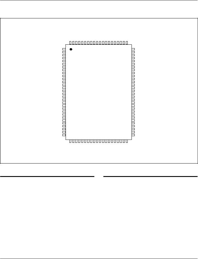
PIN CONFIGURATION
100-Pin TQFP
|
A6 |
A7 CE |
CE2 |
BWd BWc BWb BWa |
CE2 VCC |
GND CLK GW BWE OE |
ADSC ADSP ADV |
A8 |
A9 |
|
|
100 99 98 97 |
96 95 94 93 |
92 91 90 89 88 87 86 |
85 84 83 82 81 |
|
|||||
NC |
1 |
|
|
|
|
|
|
|
80 |
NC |
DQc1 |
2 |
|
|
|
|
|
|
|
79 |
DQb8 |
DQc2 |
3 |
|
|
|
|
|
|
|
78 |
DQb7 |
VCCQ |
4 |
|
|
|
|
|
|
|
77 |
VCCQ |
GND |
5 |
|
|
|
|
|
|
|
76 |
GND |
DQc3 |
6 |
|
|
|
|
|
|
|
75 |
DQb6 |
DQc4 |
7 |
|
|
|
|
|
|
|
74 |
DQb5 |
DQc5 |
8 |
|
|
|
|
|
|
|
73 |
DQb4 |
DQc6 |
9 |
|
|
|
|
|
|
|
72 |
DQb3 |
GND |
10 |
|
|
|
|
|
|
|
71 |
GND |
VCCQ |
11 |
|
|
|
|
|
|
|
70 |
VCCQ |
DQc7 |
12 |
|
|
|
|
|
|
|
69 |
DQb2 |
DQc8 |
13 |
|
|
|
|
|
|
|
68 |
DQb1 |
NC |
14 |
|
|
|
|
|
|
|
67 |
GND |
VCC |
15 |
|
|
|
|
|
|
|
66 |
NC |
NC |
16 |
|
|
|
|
|
|
|
65 |
VCC |
GND |
17 |
|
|
|
|
|
|
|
64 |
ZZ |
DQd1 |
18 |
|
|
|
|
|
|
|
63 |
DQa8 |
DQd2 |
19 |
|
|
|
|
|
|
|
62 |
DQa7 |
VCCQ |
20 |
|
|
|
|
|
|
|
61 |
VCCQ |
GND |
21 |
|
|
|
|
|
|
|
60 |
GND |
DQd3 |
22 |
|
|
|
|
|
|
|
59 |
DQa6 |
DQd4 |
23 |
|
|
|
|
|
|
|
58 |
DQa5 |
DQd5 |
24 |
|
|
|
|
|
|
|
57 |
DQa4 |
DQd6 |
25 |
|
|
|
|
|
|
|
56 |
DQa3 |
GND |
26 |
|
|
|
|
|
|
|
55 |
GND |
VCCQ |
27 |
|
|
|
|
|
|
|
54 |
VCCQ |
DQd7 |
28 |
|
|
|
|
|
|
|
53 |
DQa2 |
DQd8 |
29 |
|
|
|
|
|
|
|
52 |
DQa1 |
NC |
30 |
|
|
|
|
|
|
|
51 |
NC |
|
31 32 33 |
34 35 36 37 38 39 40 |
41 42 43 44 45 46 47 48 49 50 |
|
||||||
|
MODE |
A5 A4 |
A3 |
A2 A1 A0 NC |
NC GND |
VCC A18 A17 A10 A11 |
A12 A13 A14 |
A15 |
A16 |
|
512K x 32
PIN DESCRIPTIONS
A0, A1 |
Synchronous Address Inputs. These |
|
pins must tied to the two LSBs of the |
|
address bus. |
|
|
A2-A18 |
Synchronous Address Inputs |
|
|
ADSC |
SynchronousControllerAddressStatus |
|
|
ADSP |
SynchronousProcessorAddressStatus |
|
|
ADV |
Synchronous Burst Address Advance |
|
|
BWa-BWd |
Synchronous Byte Write Enable |
|
|
BWE |
Synchronous Byte Write Enable |
|
|
CE, CE2, CE2 |
Synchronous Chip Enable |
|
|
CLK |
Synchronous Clock |
|
|
DQa-DQd |
Synchronous Data Input/Output |
|
|
GND |
Ground |
|
|
GW |
Synchronous Global Write Enable |
|
|
MODE |
Burst Sequence Mode Selection |
|
|
OE |
Output Enable |
|
|
VCC |
+2.5V Power Supply |
|
|
VCCQ |
Isolated Output Buffer Supply: |
|
+2.5V |
|
|
ZZ |
Snooze Enable |
|
|
Integrated Silicon Solution, Inc. — 1-800-379-4774 |
3 |
ADVANCE INFORMATION Rev. 00A
05/31/01
IS61VPD51232
IS61VPD51236 ISSI®
IS61VPD10018
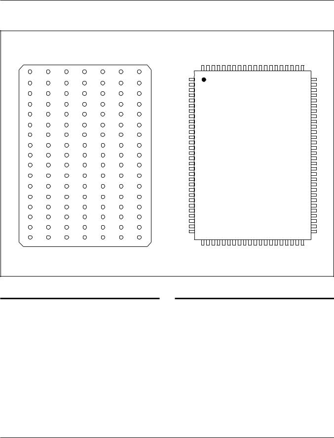
PIN CONFIGURATION
|
119-pin PBGA (Top View) |
|
|
|
|
|
|
|
100-Pin TQFP |
|
|
|
||||||
1 |
2 |
3 |
4 |
5 |
6 |
7 |
|
A6 |
A7 CE |
CE2 |
BWd |
BWc |
BWb BWa |
CE2 VCC |
GND CLK GW BWE OE |
ADSC ADSP ADV A8 |
A9 |
|
A |
|
|
|
|
|
|
|
100 99 98 97 |
96 95 94 93 |
92 91 90 89 88 87 86 |
85 84 83 82 81 |
|
||||||
VCCQ |
A6 |
A4 |
ADSP |
A8 |
A16 |
VCCQ |
DQPc |
1 |
|
|
|
|
|
|
|
|
80 |
DQPb |
B |
|
|
|
|
|
|
|
|
|
|
|
|
|
|
||||
A18 |
A3 |
ADSC |
A9 |
A17 |
NC |
DQc1 |
2 |
|
|
|
|
|
|
|
|
79 |
DQb8 |
|
NC |
DQc2 |
3 |
|
|
|
|
|
|
|
|
78 |
DQb7 |
||||||
C |
|
|
|
|
|
|
|
|
|
|
|
|
|
|
||||
A7 |
A2 |
VCC |
A12 |
A15 |
NC |
VCCQ |
4 |
|
|
|
|
|
|
|
|
77 |
VCCQ |
|
NC |
GND |
5 |
|
|
|
|
|
|
|
|
76 |
GND |
||||||
D |
|
|
|
|
|
|
|
|
|
|
|
|
|
|
||||
DQPc |
GND |
NC |
GND |
DQPb |
DQb8 |
DQc3 |
6 |
|
|
|
|
|
|
|
|
75 |
DQb6 |
|
DQc1 |
DQc4 |
7 |
|
|
|
|
|
|
|
|
74 |
DQb5 |
||||||
E |
|
|
|
|
|
|
|
|
|
|
|
|
|
|
||||
|
|
|
|
|
|
DQc5 |
8 |
|
|
|
|
|
|
|
|
73 |
DQb4 |
|
DQc2 |
DQc3 |
GND |
CE |
GND |
DQb6 |
DQb7 |
|
|
|
|
|
|
|
|
||||
DQc6 |
9 |
|
|
|
|
|
|
|
|
72 |
DQb3 |
|||||||
F |
|
|
|
|
|
|
|
|
|
|
|
|
|
|
||||
|
|
|
|
|
|
GND |
10 |
|
|
|
|
|
|
|
|
71 |
GND |
|
VCCQ |
DQc4 |
GND |
OE |
GND |
DQb5 |
VCCQ |
|
|
|
|
|
|
|
|
||||
VCCQ |
11 |
|
|
|
|
|
|
|
|
70 |
VCCQ |
|||||||
G |
|
|
|
|
|
|
|
|
|
|
|
|
|
|
||||
|
|
|
|
|
|
DQc7 |
12 |
|
|
|
|
|
|
|
|
69 |
DQb2 |
|
DQc5 |
DQc6 |
BWc |
ADV |
BWb |
DQb4 |
DQb3 |
|
|
|
|
|
|
|
|
||||
DQc8 |
13 |
|
|
|
|
|
|
|
|
68 |
DQb1 |
|||||||
H |
|
|
|
|
|
|
|
|
|
|
|
|
|
|
||||
|
|
|
|
|
|
NC |
14 |
|
|
|
|
|
|
|
|
67 |
GND |
|
DQc7 |
DQc8 |
GND |
GW |
GND |
DQb2 |
DQb1 |
|
|
|
|
|
|
|
|
||||
VCC |
15 |
|
|
|
|
|
|
|
|
66 |
NC |
|||||||
J |
|
|
|
|
|
|
|
|
|
|
|
|
|
|
||||
|
|
|
|
|
|
NC |
16 |
|
|
|
|
|
|
|
|
65 |
VCC |
|
VCCQ |
VCC |
NC |
VCC |
NC |
VCC |
VCCQ |
|
|
|
|
|
|
|
|
||||
GND |
17 |
|
|
|
|
|
|
|
|
64 |
ZZ |
|||||||
K |
|
|
|
|
|
|
|
|
|
|
|
|
|
|
||||
|
|
|
|
|
|
DQd1 |
18 |
|
|
|
|
|
|
|
|
63 |
DQa8 |
|
DQd1 |
DQd2 |
GND |
CLK |
GND |
DQa7 |
DQa8 |
|
|
|
|
|
|
|
|
||||
DQd2 |
19 |
|
|
|
|
|
|
|
|
62 |
DQa7 |
|||||||
L |
|
|
|
|
|
|
|
|
|
|
|
|
|
|
||||
|
|
|
|
|
|
VCCQ |
20 |
|
|
|
|
|
|
|
|
61 |
VCCQ |
|
DQd4 |
DQd3 |
BWd |
NC |
BWa |
DQa5 |
DQa6 |
|
|
|
|
|
|
|
|
||||
GND |
21 |
|
|
|
|
|
|
|
|
60 |
GND |
|||||||
M |
|
|
|
|
|
|
|
|
|
|
|
|
|
|
||||
|
|
|
|
|
|
DQd3 |
22 |
|
|
|
|
|
|
|
|
59 |
DQa6 |
|
VCCQ |
DQd5 |
GND |
BWE |
GND |
DQa4 |
VCCQ |
|
|
|
|
|
|
|
|
||||
DQd4 |
23 |
|
|
|
|
|
|
|
|
58 |
DQa5 |
|||||||
N |
|
|
|
|
|
|
|
|
|
|
|
|
|
|
||||
|
|
|
|
|
|
DQd5 |
24 |
|
|
|
|
|
|
|
|
57 |
DQa4 |
|
DQd6 |
DQd7 |
GND |
A1 |
GND |
DQa3 |
DQa2 |
|
|
|
|
|
|
|
|
||||
P |
|
|
|
|
|
|
DQd6 |
25 |
|
|
|
|
|
|
|
|
56 |
DQa3 |
|
|
|
|
|
|
GND |
26 |
|
|
|
|
|
|
|
|
55 |
GND |
|
DQd8 |
DQPd |
GND |
A0 |
GND |
DQPa |
DQa1 |
|
|
|
|
|
|
|
|
||||
R |
|
|
|
|
|
|
VCCQ |
27 |
|
|
|
|
|
|
|
|
54 |
VCCQ |
|
|
|
|
|
|
DQd7 |
28 |
|
|
|
|
|
|
|
|
53 |
DQa2 |
|
NC |
A5 |
MODE |
VCC |
NC |
A13 |
NC |
|
|
|
|
|
|
|
|
||||
T |
|
|
|
|
|
|
DQd8 |
29 |
|
|
|
|
|
|
|
|
52 |
DQa1 |
NC |
NC |
A10 |
A11 |
A14 |
NC |
ZZ |
DQPd |
30 |
|
|
|
|
|
|
|
|
51 |
DQPa |
U |
|
|
|
|
|
|
|
31 32 33 |
34 35 36 37 38 39 40 |
41 42 43 44 45 |
46 47 48 49 50 |
|
||||||
|
|
|
|
|
|
|
|
|
|
|
|
|
|
|
|
|
|
|
VCCQ |
TMS |
TDI |
TCK |
TDO |
NC |
VCCQ |
|
|
|
|
|
|
|
|
|
|
|
|
|
|
|
|
|
|
|
|
MODE |
A5 A4 |
A3 |
A2 |
A1 |
A0 NC |
NC GND |
VCC A18 A17 A10 A11 |
A12 A13 A14 A15 |
A16 |
|
|
|
|
|
|
|
|
512K x 36 |
|
|
|
|
|
|
|
|
|
|
|
PIN DESCRIPTIONS
A0, A1 |
Synchronous Address Inputs. These |
|
pins must tied to the two LSBs of the |
|
address bus. |
|
|
A2-A18 |
Synchronous Address Inputs |
|
|
ADSC |
SynchronousControllerAddressStatus |
|
|
ADSP |
SynchronousProcessorAddressStatus |
|
|
ADV |
SynchronousBurstAddressAdvance |
|
|
BWa-BWd |
Synchronous Byte Write Enable |
|
|
BWE |
Synchronous Byte Write Enable |
|
|
CE, CE2, CE2 |
Synchronous Chip Enable |
|
|
CLK |
Synchronous Clock |
|
|
DQa-DQd |
Synchronous Data Input/Output |
|
|
DQPa-DQPd |
Parity Data Input/Output |
|
|
GND |
Ground |
|
|
GW |
Synchronous Global Write Enable |
|
|
MODE |
Burst Sequence Mode Selection |
|
|
OE |
Output Enable |
|
|
TMS, TDI, |
JTAG Boundary Scan Pins |
TCK, TDO |
|
|
|
VCC |
+2.5V Power Supply |
|
|
VCCQ |
Isolated Output Buffer Supply: |
|
+2.5V |
|
|
ZZ |
Snooze Enable |
|
|
4 Integrated Silicon Solution, Inc. — 1-800-379-4774
ADVANCE INFORMATION Rev. 00A
05/31/01
IS61VPD51232
IS61VPD51236 ISSI®
IS61VPD10018
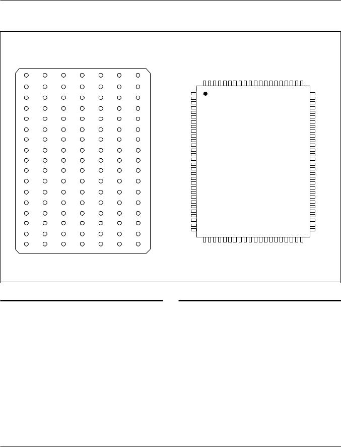
PIN CONFIGURATION
|
119-pin PBGA (Top View) |
|
|
|
|
|
|
100-Pin TQFP |
|
|
|
|
||||||
1 |
2 |
3 |
4 |
5 |
6 |
7 |
|
|
|
|
|
|
|
|
|
|
|
|
A |
A6 |
A4 |
ADSP |
A8 |
A16 |
VCCQ |
|
A6 |
A7 CE |
CE2 |
NC NC BWb BWa |
CE2 VCC |
GND CLK GW BWE OE |
ADSC ADSP |
ADV |
A8 |
A9 |
|
VCCQ |
|
|
|
|
|
|
|
|
|
|
|
|
||||||
B |
A19 |
A3 |
|
A9 |
A18 |
NC |
|
100 99 98 97 |
96 95 94 93 |
92 91 90 89 88 87 86 |
85 84 83 82 81 |
|
||||||
NC |
ADSC |
NC |
1 |
|
|
|
|
|
|
|
|
80 |
A17 |
|||||
C |
|
|
|
|
|
|
NC |
2 |
|
|
|
|
|
|
|
|
79 |
NC |
NC |
A7 |
A2 |
VCC |
A12 |
A15 |
NC |
NC |
3 |
|
|
|
|
|
|
|
|
78 |
NC |
D |
|
|
|
|
|
|
VCCQ |
4 |
|
|
|
|
|
|
|
|
77 |
VCCQ |
DQb1 |
NC |
GND |
NC |
GND |
DQPa |
NC |
GND |
5 |
|
|
|
|
|
|
|
|
76 |
GND |
E |
|
|
|
|
|
|
NC |
6 |
|
|
|
|
|
|
|
|
75 |
NC |
|
|
|
|
|
|
NC |
7 |
|
|
|
|
|
|
|
|
74 |
DQPa |
|
NC |
DQb2 |
GND |
CE |
GND |
NC |
DQa8 |
|
|
|
|
|
|
|
|
||||
DQb1 |
8 |
|
|
|
|
|
|
|
|
73 |
DQa8 |
|||||||
F |
|
|
|
|
|
|
|
|
|
|
|
|
|
|
||||
|
|
|
|
|
|
DQb2 |
9 |
|
|
|
|
|
|
|
|
72 |
DQa7 |
|
VCCQ |
NC |
GND |
OE |
GND |
DQa7 |
VCCQ |
|
|
|
|
|
|
|
|
||||
GND |
10 |
|
|
|
|
|
|
|
|
71 |
GND |
|||||||
G |
|
|
|
|
|
|
|
|
|
|
|
|
|
|
||||
|
|
|
|
|
|
VCCQ |
11 |
|
|
|
|
|
|
|
|
70 |
VCCQ |
|
NC |
DQb3 |
BWb |
ADV |
GND |
NC |
DQa6 |
DQb3 |
12 |
|
|
|
|
|
|
|
|
69 |
DQa6 |
H |
|
|
|
|
|
|
DQb4 |
13 |
|
|
|
|
|
|
|
|
68 |
DQa5 |
DQb4 |
NC |
GND |
GW |
GND |
DQa5 |
NC |
NC |
14 |
|
|
|
|
|
|
|
|
67 |
GND |
J |
|
|
|
|
|
|
VCC |
15 |
|
|
|
|
|
|
|
|
66 |
NC |
|
|
|
|
|
|
NC |
16 |
|
|
|
|
|
|
|
|
65 |
VCC |
|
VCCQ |
VCC |
NC |
VCC |
NC |
VCC |
VCCQ |
|
|
|
|
|
|
|
|
||||
K |
|
|
|
|
|
|
GND |
17 |
|
|
|
|
|
|
|
|
64 |
ZZ |
|
|
|
|
|
|
DQb5 |
18 |
|
|
|
|
|
|
|
|
63 |
DQa4 |
|
NC |
DQb5 |
GND |
CLK |
GND |
NC |
DQa4 |
|
|
|
|
|
|
|
|
||||
DQb6 |
19 |
|
|
|
|
|
|
|
|
62 |
DQa3 |
|||||||
L |
|
|
|
|
|
|
|
|
|
|
|
|
|
|
||||
|
|
|
|
|
|
VCCQ |
20 |
|
|
|
|
|
|
|
|
61 |
VCCQ |
|
DQb6 |
NC |
GND |
NC |
BWa |
DQa3 |
NC |
GND |
21 |
|
|
|
|
|
|
|
|
60 |
GND |
M |
|
|
|
|
|
|
DQb7 |
22 |
|
|
|
|
|
|
|
|
59 |
DQa2 |
VCCQ |
DQb7 |
GND |
BWE |
GND |
NC |
VCCQ |
DQb8 |
23 |
|
|
|
|
|
|
|
|
58 |
DQa1 |
N |
|
|
|
|
|
|
DQPb |
24 |
|
|
|
|
|
|
|
|
57 |
NC |
DQb8 |
NC |
GND |
A1 |
GND |
DQa2 |
NC |
NC |
25 |
|
|
|
|
|
|
|
|
56 |
NC |
P |
|
|
|
|
|
|
GND |
26 |
|
|
|
|
|
|
|
|
55 |
GND |
|
|
|
|
|
|
VCCQ |
27 |
|
|
|
|
|
|
|
|
54 |
VCCQ |
|
NC |
DQPb |
GND |
A0 |
GND |
NC |
DQa1 |
|
|
|
|
|
|
|
|
||||
NC |
28 |
|
|
|
|
|
|
|
|
53 |
NC |
|||||||
R |
|
|
|
|
|
|
|
|
|
|
|
|
|
|
||||
|
|
|
|
|
|
NC |
29 |
|
|
|
|
|
|
|
|
52 |
NC |
|
NC |
A5 |
MODE |
VCC |
NC |
A13 |
NC |
|
|
|
|
|
|
|
|
||||
NC |
30 |
|
|
|
|
|
|
|
|
51 |
NC |
|||||||
T |
|
|
|
|
|
|
|
|
|
|
|
|
|
|
||||
|
|
|
|
|
|
|
31 32 33 |
34 35 36 37 38 39 40 |
41 42 43 44 45 46 47 48 49 50 |
|
||||||||
NC |
A11 |
A10 |
NC |
A14 |
A17 |
ZZ |
|
|
|
|
|
|
|
|
|
|
|
|
U |
|
|
|
|
|
|
|
MODE |
A5 A4 |
A3 |
A2 A1 A0 NC |
NC GND |
VCC A19 A18 A10 A11 |
A12 A13 |
A14 |
A15 |
A16 |
|
VCCQ |
TMS |
TDI |
TCK |
TDO |
NC |
VCCQ |
|
|
||||||||||
|
|
|
|
|
|
|
|
|
||||||||||
|
|
|
|
|
|
|
1024K x 18 |
|
|
|
|
|
|
|
|
|
|
|
PIN DESCRIPTIONS
A0, A1 |
Synchronous Address Inputs. These |
|
pins must tied to the two LSBs of the |
|
address bus. |
|
|
A2-A19 |
Synchronous Address Inputs |
|
|
ADSC |
SynchronousControllerAddressStatus |
|
|
ADSP |
SynchronousProcessorAddressStatus |
|
|
ADV |
SynchronousBurstAddressAdvance |
|
|
BWa-BWd |
Synchronous Byte Write Enable |
|
|
BWE |
Synchronous Byte Write Enable |
|
|
CE, CE2, CE2 |
Synchronous Chip Enable |
|
|
CLK |
Synchronous Clock |
|
|
DQa-DQd |
Synchronous Data Input/Output |
|
|
DQPa-DQPb |
Parity Data I/O; DQPa is parity for |
|
DQa1-8; DQPb is parity for DQb1-8 |
|
|
GND |
Ground |
|
|
GW |
Synchronous Global Write Enable |
|
|
MODE |
Burst Sequence Mode Selection |
|
|
OE |
Output Enable |
|
|
TMS, TDI, |
JTAG Boundary Scan Pins |
TCK, TDO |
|
|
|
VCC |
+2.5V Power Supply |
|
|
VCCQ |
Isolated Output Buffer Supply: |
|
+2.5V |
|
|
ZZ |
Snooze Enable |
|
|
Integrated Silicon Solution, Inc. — 1-800-379-4774 |
5 |
ADVANCE INFORMATION Rev. 00A
05/31/01

IS61VPD51232
IS61VPD51236 ISSI®
IS61VPD10018
TRUTH TABLE(1-8) (3CE option)
OPERATION |
ADDRESS |
CE |
CE2 |
CE2 |
ZZ |
ADSP |
ADSC |
ADV |
WRITE |
OE |
CLK |
DQ |
|
|
|
|
|
|
|
|
|
|
|
|
|
Deselect Cycle, Power-Down |
None |
H |
X |
X |
L |
X |
L |
X |
X |
X |
L-H |
High-Z |
|
|
|
|
|
|
|
|
|
|
|
|
|
Deselect Cycle, Power-Down |
None |
L |
X |
L |
L |
L |
X |
X |
X |
X |
L-H |
High-Z |
|
|
|
|
|
|
|
|
|
|
|
|
|
Deselect Cycle, Power-Down |
None |
L |
H |
X |
L |
L |
X |
X |
X |
X |
L-H |
High-Z |
|
|
|
|
|
|
|
|
|
|
|
|
|
Deselect Cycle, Power-Down |
None |
L |
X |
L |
L |
H |
L |
X |
X |
X |
L-H |
High-Z |
|
|
|
|
|
|
|
|
|
|
|
|
|
Deselect Cycle, Power-Down |
None |
L |
H |
X |
L |
H |
L |
X |
X |
X |
L-H |
High-Z |
|
|
|
|
|
|
|
|
|
|
|
|
|
Snooze Mode, Power-Down |
None |
X |
X |
X |
H |
X |
X |
X |
X |
X |
X |
High-Z |
|
|
|
|
|
|
|
|
|
|
|
|
|
Read Cycle, Begin Burst |
External |
L |
L |
H |
L |
L |
X |
X |
X |
L |
L-H |
Q |
|
|
|
|
|
|
|
|
|
|
|
|
|
Read Cycle, Begin Burst |
External |
L |
L |
H |
L |
L |
X |
X |
X |
H |
L-H |
High-Z |
|
|
|
|
|
|
|
|
|
|
|
|
|
Write Cycle, Begin Burst |
External |
L |
L |
H |
L |
H |
L |
X |
L |
X |
L-H |
D |
|
|
|
|
|
|
|
|
|
|
|
|
|
Read Cycle, Begin Burst |
External |
L |
L |
H |
L |
H |
L |
X |
H |
L |
L-H |
Q |
|
|
|
|
|
|
|
|
|
|
|
|
|
Read Cycle, Begin Burst |
External |
L |
L |
H |
L |
H |
L |
X |
H |
H |
L-H |
High-Z |
|
|
|
|
|
|
|
|
|
|
|
|
|
Read Cycle, Continue Burst |
Next |
X |
X |
X |
L |
H |
H |
L |
H |
L |
L-H |
Q |
|
|
|
|
|
|
|
|
|
|
|
|
|
Read Cycle, Continue Burst |
Next |
X |
X |
X |
L |
H |
H |
L |
H |
H |
L-H |
High-Z |
|
|
|
|
|
|
|
|
|
|
|
|
|
Read Cycle, Continue Burst |
Next |
H |
X |
X |
L |
X |
H |
L |
H |
L |
L-H |
Q |
|
|
|
|
|
|
|
|
|
|
|
|
|
Read Cycle, Continue Burst |
Next |
H |
X |
X |
L |
X |
H |
L |
H |
H |
L-H |
High-Z |
|
|
|
|
|
|
|
|
|
|
|
|
|
Write Cycle, Continue Burst |
Next |
X |
X |
X |
L |
H |
H |
L |
L |
X |
L-H |
D |
|
|
|
|
|
|
|
|
|
|
|
|
|
Write Cycle, Continue Burst |
Next |
H |
X |
X |
L |
X |
H |
L |
L |
X |
L-H |
D |
|
|
|
|
|
|
|
|
|
|
|
|
|
Read Cycle, Suspend Burst |
Current |
X |
X |
X |
L |
H |
H |
H |
H |
L |
L-H |
Q |
|
|
|
|
|
|
|
|
|
|
|
|
|
Read Cycle, Suspend Burst |
Current |
X |
X |
X |
L |
H |
H |
H |
H |
H |
L-H |
High-Z |
|
|
|
|
|
|
|
|
|
|
|
|
|
Read Cycle, Suspend Burst |
Current |
H |
X |
X |
L |
X |
H |
H |
H |
L |
L-H |
Q |
|
|
|
|
|
|
|
|
|
|
|
|
|
Read Cycle, Suspend Burst |
Current |
H |
X |
X |
L |
X |
H |
H |
H |
H |
L-H |
High-Z |
|
|
|
|
|
|
|
|
|
|
|
|
|
Write Cycle, Suspend Burst |
Current |
X |
X |
X |
L |
H |
H |
H |
L |
X |
L-H |
D |
|
|
|
|
|
|
|
|
|
|
|
|
|
Write Cycle, Suspend Burst |
Current |
H |
X |
X |
L |
X |
H |
H |
L |
X |
L-H |
D |
|
|
|
|
|
|
|
|
|
|
|
|
|
NOTE:
1.X means “Don’t Care.” H means logic HIGH. L means logic LOW.
2.For WRITE, L means one or more byte write enable signals (BWa, BWb, BWc or BWd) and BWE are LOW or GW is LOW. WRITE = H for all BWx, BWE, GW HIGH.
3.BWa enables WRITEs to DQa’s and DQPa. BWb enables WRITEs to DQb’s and DQPb. BWc enables WRITEs to DQc’s and DQPc. BWd enables WRITEs to DQd’s and DQPd. DQPa and DQPb are only available on the x18 and x36 versions. DQPc and DQPd are only available on the x36 version.
4.All inputs except OE and ZZ must meet setup and hold times around the rising edge (LOW to HIGH) of CLK.
5.Wait states are inserted by suspending burst.
6.For a WRITE operation following a READ operation, OE must be HIGH before the input data setup time and held HIGH during the input data hold time.
7.This device contains circuitry that will ensure the outputs will be in High-Z during power-up.
8.ADSP LOW always initiates an internal READ at the L-H edge of CLK. A WRITE is performed by setting one or more byte write enable signals and BWE LOW or GW LOW for the subsequent L-H edge of CLK. See WRITE timing diagram for clarification.
6 Integrated Silicon Solution, Inc. — 1-800-379-4774
ADVANCE INFORMATION Rev. 00A
05/31/01

IS61VPD51232 |
ISSI |
|
IS61VPD51236 |
® |
|
IS61VPD10018 |
|
TRUTH TABLE(1-8) (1CE option)
NEXT CYCLE |
ADDRESS |
CE |
ADSP |
ADSC |
ADV |
WRITE |
OE |
DQ |
|
|
|
|
|
|
|
|
|
Deselected |
None |
H |
X |
L |
X |
X |
X |
High-Z |
|
|
|
|
|
|
|
|
|
Read, Begin |
External |
L |
L |
X |
X |
X |
L |
Q |
|
|
|
|
|
|
|
|
|
Read, Begin |
External |
L |
L |
X |
X |
X |
H |
High-Z |
|
|
|
|
|
|
|
|
|
Write, Begin |
Current |
L |
H |
L |
X |
Write |
X |
D |
|
|
|
|
|
|
|
|
|
Read, Begin |
External |
L |
H |
L |
X |
Read |
L |
Q |
|
|
|
|
|
|
|
|
|
Read, Begin |
External |
L |
H |
L |
X |
Read |
H |
High-Z |
|
|
|
|
|
|
|
|
|
Read, Burst |
Next |
X |
H |
H |
L |
Read |
L |
Q |
|
|
|
|
|
|
|
|
|
Read, Burst |
Next |
X |
H |
H |
L |
Read |
H |
High-Z |
|
|
|
|
|
|
|
|
|
Read, Burst |
Next |
H |
X |
H |
L |
Read |
L |
Q |
|
|
|
|
|
|
|
|
|
Read, Burst |
Next |
H |
X |
H |
L |
Read |
H |
High-Z |
|
|
|
|
|
|
|
|
|
Write, Burst |
Next |
X |
H |
H |
L |
Write |
X |
D |
|
|
|
|
|
|
|
|
|
Write, Burst |
Next |
H |
X |
H |
L |
Write |
X |
D |
|
|
|
|
|
|
|
|
|
Read, Suspend |
Current |
X |
H |
H |
H |
Read |
L |
Q |
|
|
|
|
|
|
|
|
|
Read, Suspend |
Current |
X |
H |
H |
H |
Read |
H |
High-Z |
|
|
|
|
|
|
|
|
|
Read, Suspend |
Current |
H |
X |
H |
H |
Read |
L |
Q |
|
|
|
|
|
|
|
|
|
Read, Suspend |
Current |
H |
X |
H |
H |
Read |
H |
High-Z |
|
|
|
|
|
|
|
|
|
Write, Suspend |
Current |
X |
H |
H |
H |
Write |
X |
D |
|
|
|
|
|
|
|
|
|
Write, Suspend |
Current |
H |
X |
H |
H |
Write |
X |
D |
|
|
|
|
|
|
|
|
|
NOTE:
1.X means “Don’t Care.” H means logic HIGH. L means logic LOW.
2.For WRITE, L means one or more byte write enable signals (BWa, BWb, BWc or BWd) and BWE are LOW or GW is LOW. WRITE = H for all BWx, BWE, GW HIGH.
3.BWa enables WRITEs to DQa’s and DQPa. BWb enables WRITEs to DQb’s and DQPb. BWc enables WRITEs to DQc’s and DQPc. BWd enables WRITEs to DQd’s and DQPd. DQPa and DQPb are only available on the x18 and x36 versions. DQPc and DQPd are only available on the x36 version.
4.All inputs except OE and ZZ must meet setup and hold times around the rising edge (LOW to HIGH) of CLK.
5.Wait states are inserted by suspending burst.
6.For a WRITE operation following a READ operation, OE must be HIGH before the input data setup time and held HIGH during the input data hold time.
7.This device contains circuitry that will ensure the outputs will be in High-Z during power-up.
8.ADSP LOW always initiates an internal READ at the L-H edge of CLK. A WRITE is performed by setting one or more byte write enable signals and BWE LOW or GW LOW for the subsequent L-H edge of CLK. See WRITE timing diagram for clarification.
PARTIAL TRUTH TABLE
|
Function |
GW |
BWE |
BWa |
BWb |
BWc |
BWd |
|
|
|
|
|
|
|
|
|
|
|
Read |
H |
H |
X |
X |
X |
X |
|
|
|
|
|
|
|
|
|
|
|
Read |
H |
L |
H |
H |
H |
H |
|
|
Write Byte 1 |
H |
L |
L |
H |
H |
H |
|
|
Write All Bytes |
H |
L |
L |
L |
L |
L |
|
|
|
|
|
|
|
|
|
|
|
Write All Bytes |
L |
X |
X |
X |
X |
X |
|
|
|
|
|
|
||||
|
|
|
|
|
|
|
|
|
Integrated Silicon Solution, Inc. — 1-800-379-4774 |
|
7 |
||||||
ADVANCE INFORMATION |
Rev. 00A |
|
|
|
|
|
|
|
05/31/01 |
|
|
|
|
|
|
|
|
IS61VPD51232
IS61VPD51236 ISSI®
IS61VPD10018
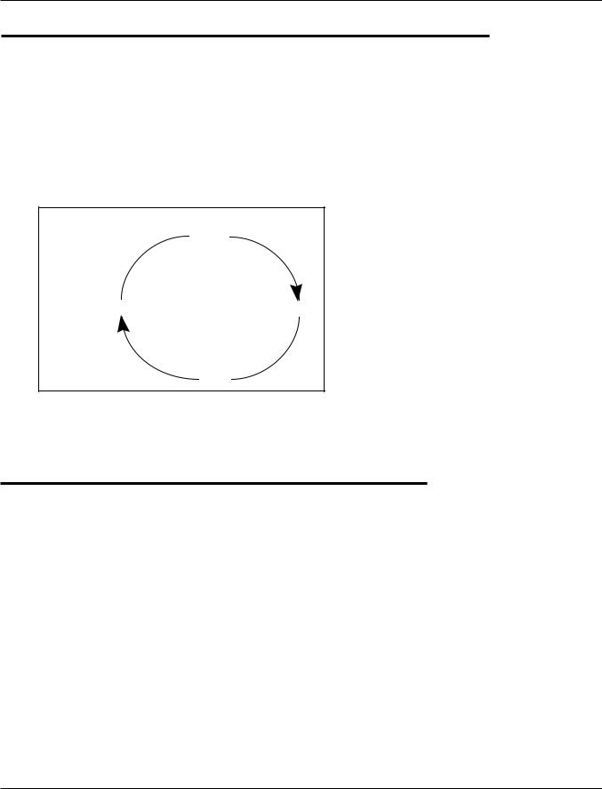
INTERLEAVED BURST ADDRESS TABLE (MODE = VCC or No Connect)
External Address |
1st Burst Address |
2nd Burst Address |
3rd Burst Address |
A1 A0 |
A1 A0 |
A1 A0 |
A1 A0 |
|
|
|
|
00 |
01 |
10 |
11 |
|
|
|
|
01 |
00 |
11 |
10 |
10 |
11 |
00 |
01 |
|
|
|
|
11 |
10 |
01 |
00 |
|
|
|
|
LINEAR BURST ADDRESS TABLE (MODE = GND)
 0,0
0,0
A1', A0' = 1,1 |
0,1 |
1,0
ABSOLUTE MAXIMUM RATINGS(1)
Symbol |
Parameter |
Value |
Unit |
TBIAS |
Temperature Under Bias |
–40 to +85 |
°C |
|
|
|
|
TSTG |
Storage Temperature |
–55 to +150 |
°C |
|
|
|
|
PD |
Power Dissipation |
1.6 |
W |
|
|
|
|
IOUT |
Output Current (per I/O) |
100 |
mA |
|
|
|
|
VIN, VOUT |
Voltage Relative to GND for I/O Pins |
–0.5 to VCCQ + 0.5 |
V |
|
|
|
|
VIN |
Voltage Relative to GND for |
–0.5 to VCC + 0.5 |
V |
|
for Address and Control Inputs |
|
|
|
|
|
|
VCC |
Voltage on Vcc Supply Relatiive to GND |
–0.5 to 3.2 |
V |
|
|
|
|
Notes:
1.Stress greater than those listed under ABSOLUTE MAXIMUM RATINGS may cause permanent damage to the device. This is a stress rating only and functional operation of the device at these or any other conditions above those indicated in the operational sections of this specification is not implied. Exposure to absolute maximum rating conditions for extended periods may affect reliability.
2.This device contains circuity to protect the inputs against damage due to high static voltages or electric fields; however, precautions may be taken to avoid application of any voltage higher than maximum rated voltages to this high-impedance circuit.
3.This device contains circuitry that will ensure the output devices are in High-Z at power up.
8 Integrated Silicon Solution, Inc. — 1-800-379-4774
ADVANCE INFORMATION Rev. 00A
05/31/01
 Loading...