


ISSI IS42S32200A-7TI, IS42S32200A-6T, IS42S32200A-5TI, IS42S32200A-5T, IS42S32200A-7T Datasheet
...IS42S32200A |
ISSI® |
512 Meg Bits x 32 Bits x 4 Banks (64-MBIT) SYNCHRONOUS DYNAMIC RAM
ADVANCED INFORMATION
JULY 2001
FEATURES
•Clock frequency: 200, 166, 143 MHz
•Fully synchronous; all signals referenced to a positive clock edge
•Internal bank for hiding row access/precharge
•Single 3.3V power supply
•LVTTL interface
•Programmable burst length
– (1, 2, 4, 8, full page)
•Programmable burst sequence: Sequential/Interleave
•Self refresh modes
•4096 refresh cycles every 64 ms
•Random column address every clock cycle
•Programmable CAS latency (2, 3 clocks)
•Burst read/write and burst read/single write operations capability
•Burst termination by burst stop and precharge command
•Industrial temperature availability
•Package 400-mil 86-pin TSOP II
PIN DESCRIPTIONS
A0-A10 |
Address Input |
BA0, BA1 |
Bank Select Address |
|
|
I/O0 to I/O31 |
Data I/O |
|
|
CLK |
System Clock Input |
|
|
CKE |
Clock Enable |
|
|
CS |
Chip Select |
|
|
RAS |
Row Address Strobe Command |
|
|
CAS |
Column Address Strobe Command |
|
|
OVERVIEW
ISSI's 64Mb Synchronous DRAM IS42S32200A is organized as 524,288 bits x 32-bit x 4-bank for improved performance. ThesynchronousDRAMsachievehigh-speed data transfer using pipeline architecture. All inputs and outputs signals refer to the rising edge of the clock input.
PIN CONFIGURATION
(86-Pin TSOP (Type II)
|
|
|
|
|
|
|
|
|
VCC |
|
|
1 |
86 |
|
|
GND |
|
I/O0 |
|
|
|
85 |
|
|
I/O15 |
|
|
|
|
2 |
|
|
|||
VCCQ |
|
|
|
84 |
|
|
GNDQ |
|
|
|
|
3 |
|
|
|||
I/O1 |
|
|
|
83 |
|
|
I/O14 |
|
|
|
|
4 |
|
|
|||
I/O2 |
|
|
|
82 |
|
|
I/O13 |
|
|
|
|
5 |
|
|
|||
GNDQ |
|
|
|
81 |
|
|
VCCQ |
|
|
|
|
6 |
|
|
|||
I/O3 |
|
|
|
80 |
|
|
I/O12 |
|
|
|
|
7 |
|
|
|||
I/O4 |
|
|
|
8 |
79 |
|
|
I/O11 |
|
|
|
|
|
||||
VCCQ |
|
|
|
78 |
|
|
GNDQ |
|
|
|
|
9 |
|
|
|||
I/O5 |
|
|
|
77 |
|
|
I/O10 |
|
|
|
|
10 |
|
|
|||
I/O6 |
|
|
|
76 |
|
|
I/O9 |
|
|
|
|
11 |
|
|
|||
GNDQ |
|
|
|
75 |
|
|
VCCQ |
|
|
|
|
12 |
|
|
|||
I/O7 |
|
|
|
13 |
74 |
|
|
I/O8 |
|
|
|
|
|||||
NC |
|
|
|
14 |
73 |
|
|
NC |
|
|
|
|
|||||
VCC |
|
|
|
15 |
72 |
|
|
GND |
|
|
|
|
|||||
DQM0 |
|
|
|
16 |
71 |
|
|
DQM1 |
|
|
|
|
|||||
WE |
|
|
|
17 |
70 |
|
|
NC |
|
|
|
|
|||||
CAS |
|
|
|
18 |
69 |
|
|
NC |
|
|
|
|
|||||
RAS |
|
|
|
19 |
68 |
|
|
CLK |
|
|
|
|
|||||
CS |
|
|
|
20 |
67 |
|
|
CKE |
|
|
|
|
|||||
NC |
|
|
|
21 |
66 |
|
|
A9 |
|
|
|
|
|||||
BA0 |
|
|
|
22 |
65 |
|
|
A8 |
|
|
|
|
|||||
BA1 |
|
|
|
23 |
64 |
|
|
A7 |
|
|
|
|
|||||
A10/AP |
|
|
|
24 |
63 |
|
|
A6 |
|
|
|
|
|||||
A0 |
|
|
|
62 |
|
|
A5 |
|
|
|
|
25 |
|
|
|||
|
|
|
|
|
|
|
||
A1 |
|
|
26 |
61 |
|
|
A4 |
|
|
|
|
|
|
|
|||
A2 |
|
|
27 |
60 |
|
|
A3 |
|
DQM2 |
|
28 |
59 |
|
|
DQM3 |
||
VCC |
|
|
|
29 |
58 |
|
|
GND |
|
|
|
|
|||||
NC |
|
30 |
57 |
|
|
NC |
||
|
|
|
|
|||||
I/O16 |
|
31 |
56 |
|
|
I/O31 |
||
|
|
|
|
|||||
GNDQ |
|
32 |
55 |
|
|
VCCQ |
||
|
|
|
|
|||||
I/O17 |
|
33 |
54 |
|
|
I/O30 |
||
|
|
|
|
|||||
I/O18 |
|
34 |
53 |
|
|
I/O29 |
||
|
|
|
|
|||||
VCCQ |
|
35 |
53 |
|
|
GNDQ |
||
|
|
|
|
|||||
I/O19 |
|
36 |
51 |
|
|
I/O28 |
||
|
|
|
|
|||||
I/O20 |
|
37 |
50 |
|
|
I/O27 |
||
|
|
|
|
|||||
GNDQ |
|
38 |
49 |
|
|
VCCQ |
||
|
|
|
|
|||||
I/O21 |
|
39 |
48 |
|
|
I/O26 |
||
|
|
|
|
|||||
I/O22 |
|
40 |
47 |
|
|
I/O25 |
||
|
|
|
|
|||||
VCCQ |
|
41 |
46 |
|
|
GNDQ |
||
|
|
|
|
|||||
I/O23 |
|
42 |
45 |
|
|
I/O24 |
||
|
|
|
|
|
|
|||
VCC |
|
|
43 |
44 |
|
|
GND |
|
|
|
|
|
|
|
|
|
|
WE |
Write Enable |
|
|
DQM0 to DQM3 |
Input/Output Mask |
|
|
Vcc |
Power |
|
|
GND |
Ground |
|
|
VccQ |
Power Supply for I/O Pin |
|
|
GNDQ |
Ground for I/O Pin |
|
|
NC |
No Connection |
|
|
This document contains TARGET SPECIFICATION data. ISSI reserves the right to make changes to its products at any time without notice in order to improve design and supply the best possible product. We assume no responsibility for any errors which may appear in this publication. © Copyright 2001, Integrated Silicon Solution, Inc.
Integrated Silicon Solution, Inc. — 1-800-379-4774 |
1 |
TARGET SPECIFICATION Rev. 00A
07/01/01

IS42S32200A |
ISSI® |
GENERAL DESCRIPTION
The 64Mb SDRAM is a high speed CMOS, dynamic random-access memory designed to operate in 3.3V memory systems containing 67,108,864 bits. Internally configured as a quad-bank DRAM with a synchronous interface. Each 16,777,216-bit bank is organized as 2,048 rows by 256 columns by 32 bits.
The 64Mb SDRAM includes an AUTO REFRESH MODE, and a power-saving, power-down mode. All signals are registered on the positive edge of the clock signal, CLK. All inputs and outputs are LVTTL compatible.
The 64Mb SDRAM has the ability to synchronously burst data at a high data rate with automatic column-address generation, the ability to interleave between internal banks to hide precharge time and the capability to randomly change column addresses on each clock cycle during burst access.
A self-timed row precharge initiated at the end of the burst sequence is available with the AUTO PRECHARGE
function enabled. Precharge one bank while accessing one of the other three banks will hide the precharge cycles and provide seamless, high-speed, random-access operation.
SDRAM read and write accesses are burst oriented starting at a selected location and continuing for a programmed number of locations in a programmed sequence. The registration of an ACTIVE command begins accesses, followed by a READ or WRITE command. The ACTIVE command in conjunction with address bits registered are used to select the bank and row to be accessed (BA0, BA1 select the bank; A0-A10 select the row). The READ or WRITE commands in conjunction with address bits registered are used to select the starting column location for the burst access.
Programmable READ or WRITE burst lengths consist of 1, 2, 4 and 8 locations or full page, with a burst terminate option.
FUNCTIONAL BLOCK DIAGRAM
CLK |
|
|
|
|
|
|
CKE |
|
|
|
|
|
|
CS |
COMMAND |
|
|
|
|
|
RAS |
DECODER |
|
|
|
|
|
CAS |
|
& |
|
|
|
|
WE |
CLOCK |
MODE |
|
REFRESH |
|
|
|
GENERATOR |
|
CONTROLLER |
|
||
|
REGISTER |
|
|
|||
|
|
|
|
|
||
|
|
|
|
|
|
|
|
|
|
10 |
|
SELF |
|
|
|
|
|
|
|
|
A10 |
|
|
|
|
REFRESH |
|
|
|
|
|
CONTROLLER |
|
|
|
|
|
|
|
|
|
A9 |
|
|
|
|
|
|
A8 |
|
|
|
|
|
|
A7 |
|
|
|
|
REFRESH |
|
A6 |
|
|
|
|
|
|
|
|
|
|
COUNTER |
|
|
A5 |
|
|
|
|
|
|
A4 |
|
|
|
MULTIPLEXER |
|
DECODERROW |
A3 |
|
|
|
|
||
|
|
|
|
|
|
|
A2 |
|
|
|
|
|
|
A1 |
|
|
|
|
|
10 |
A0 |
|
|
|
|
|
|
|
ROW |
|
|
|
|
|
BA0 |
|
|
|
ROW |
|
|
BA1 |
|
ADDRESS |
|
ADDRESS |
|
|
|
10 |
LATCH |
|
|
BUFFER |
|
|
|
|
|
10 |
|
|
|
|
|
|
|
|
|
|
|
|
COLUMN |
|
|
BANK CONTROL LOGIC |
|
|
|
ADDRESS LATCH |
|
|
|
|
|
|
|
|
|
|
|
|
|
BURST COUNTER |
|
|
|
|
|
|
COLUMN |
|
|
|
|
|
|
ADDRESS BUFFER |
|
|
|
|
|
|
|
|
|
|
DQM0-3 |
||
|
|
DATA IN |
|
|
|
|
|
|
|
|
|
BUFFER |
|
|
|
|
|
|
|
32 |
|
|
|
32 |
|
|
|
I/O 0-31 |
|
|
|
|
|
|
|
|
|
||
|
|
|
|
|
|
|
|
||
|
|
|
|
|
|
|
|
||
|
|
|
|
|
|
|
|||
|
|
|
|
|
|
|
|
|
Vcc/VccQ |
|
DATA OUT |
|
|
|
|
|
|||
|
|
|
|
|
|
||||
|
|
|
|
|
|
|
|||
32 |
BUFFER |
32 |
|
|
|
|
GND/GNDQ |
||
|
|
|
|
||||||
|
|
|
|
|
|
|
|
||
2048 |
|
|
2048 |
MEMORY CELL |
|
2048 |
||
ARRAY |
||
2048 |
||
|
BANK 0
SENSE AMP I/O GATE
256 (x 32)
COLUMN DECODER
2 Integrated Silicon Solution, Inc. — 1-800-379-4774
TARGET SPECIFICATION Rev. 00A
07/01/01

IS42S32200A |
|
ISSI® |
|
PIN FUNCTIONS |
|
|
|
|
|
|
|
Symbol |
Pin No. |
Type |
Function (In Detail) |
|
|
|
|
A0-A10 |
25 to 27 |
Input Pin |
Address Inputs: A0-A10 are sampled during the ACTIVE |
|
60 to 66 |
|
command (row-address A0-A10) and READ/WRITE command (A0-A7 |
|
24 |
|
with A10 defining auto precharge) to select one location out of the memory array |
|
|
|
in the respective bank. A10 is sampled during a PRECHARGE command to |
|
|
|
determine if all banks are to be precharged (A10 HIGH) or bank selected by |
|
|
|
BA0, BA1 (LOW). The address inputs also provide the op-code during a LOAD |
|
|
|
MODE REGISTER command. |
|
|
|
|
BA0, BA1 |
22,23 |
Input Pin |
Bank Select Address: BA0 and BA1 defines which bank the ACTIVE, READ, |
|
|
|
WRITE or PRECHARGE command is being applied. |
|
|
|
|
CAS |
18 |
Input Pin |
CAS, in conjunction with the RAS and WE, forms the device command. See the |
|
|
|
"Command Truth Table" for details on device commands. |
|
|
|
|
CKE |
67 |
Input Pin |
The CKE input determines whether the CLK input is enabled. The next rising edge |
|
|
|
of the CLK signal will be valid when is CKE HIGH and invalid when LOW. When |
|
|
|
CKE is LOW, the device will be in either power-down mode, clock suspend mode, |
|
|
|
or self refresh mode. CKE is an asynchronous input. |
|
|
|
|
CLK |
68 |
Input Pin |
CLK is the master clock input for this device. Except for CKE, all inputs to this |
|
|
|
device are acquired in synchronization with the rising edge of this pin. |
|
|
|
|
CS |
20 |
Input Pin |
The CS input determines whether command input is enabled within the device. |
|
|
|
Command input is enabled when CS is LOW, and disabled with CS is HIGH. The |
|
|
|
device remains in the previous state when CS is HIGH. |
|
|
|
|
I/O0 to |
2, 4, 5, 7, 8, 10,11,13 |
I/O Pin |
I/O0 to I/O15 are I/O pins. I/O through these pins can be controlled in byte units |
I/O31 |
74,76,77,79,80,82,83,85 |
|
using the DQM0-DQM3 pins |
|
45,47,48,50,51,53,54,56 |
|
|
|
31,33,34,36,37,39,40,42 |
|
|
|
|
|
|
DQM0 |
16,28,59,71 |
Input Pin |
DQMx control thel ower and upper bytes of the I/O buffers. In read mode, |
DQM3 |
|
|
the output buffers are place in a High-Z state. During a WRITE cycle the input data |
|
|
|
is masked. When DQMx is sampled HIGH and is an input mask signal for write |
|
|
|
accesses and an output enable signal for read accesses. I/O0 through I/O7 are |
|
|
|
controlled by DQM0. I/O8 throughI/O15 are controlled by DQM1. I/O16 through I/ |
|
|
|
O23 are controlled by DQM2. I/O24 through I/O31 are controlled by DQM3. |
|
|
|
|
RAS |
19 |
Input Pin |
RAS, in conjunction with CAS and WE, forms the device command. See the |
|
|
|
"Command Truth Table" item for details on device commands. |
|
|
|
|
WE |
17 |
Input Pin |
WE, in conjunction with RAS and CAS, forms the device command. See the |
|
|
|
"Command Truth Table" item for details on device commands. |
|
|
|
|
VCCQ |
3,9,35,41,49,55,25,81 |
Supply Pin |
VCCQ is the output buffer power supply. |
|
|
|
|
VCC |
1,15,29,43 |
Supply Pin |
VCC is the device internal power supply. |
|
|
|
|
GNDQ |
6,12,32,38,46,52,78,84 |
Supply Pin |
GNDQ is the output buffer ground. |
|
|
|
|
GND |
44,58,72,86 |
Supply Pin |
GND is the device internal ground. |
|
|
|
|
Integrated Silicon Solution, Inc. — 1-800-379-4774 |
3 |
TARGET SPECIFICATION Rev. 00A
07/01/01

IS42S32200A |
ISSI® |
FUNCTION (In Detail)
A0-A10 are address inputs sampled during the ACTIVE (row-address A0-A10) and READ/WRITE command (A0-A7 with A10 defining auto PRECHARGE). A10 is sampled during a PRECHARGE command to determine if all banks are to be PRECHARGED (A10 HIGH) or bank selected by BA0, BA1 (LOW). The address inputs also provide the op-code during a LOAD MODE REGISTER command.
Bank Select Address (BA0 and BA1) defines which bank the ACTIVE, READ, WRITE or PRECHARGE command is being applied.
CAS, in conjunction with the RAS and WE, forms the device command. See the “Command Truth Table” for details on device commands.
The CKE input determines whether the CLK input is enabled. The next rising edge of the CLK signal will be valid when is CKE HIGH and invalid when LOW. When CKE is LOW, the device will be in either power-down mode, CLOCK SUSPEND mode, or SELF-REFRESH mode. CKE is an asynchronous input.
CLK is the master clock input for this device. Except for CKE, all inputs to this device are acquired in synchronization with the rising edge of this pin.
The CS input determines whether command input is enabled within the device. Command input is enabled when CS is LOW, and disabled with CS is HIGH. The device remains in the previous state when CS is HIGH. I I/O0 through I/O7 are controlled by DQM0. I/O8 through I/O15 are controlled by DQM1. I/O16 through I/O23 are controlled by DQM2. I/O24 through I/O31 are controlled by DQM3. In read mode, DQMx control the output buffer. When DQMx is LOW, the corresponding buffer byte is enabled, and when HIGH, disabled. The outputs go to the HIGH Impedance State when DQMx is HIGH. This function corresponds to OE in conventional DRAMs. In write mode, DQMx control the input buffer. When DQMx is LOW, the corresponding buffer byte is enabled, and data can be written to the device. When DQMx is HIGH, input data is masked and cannot be written to the device.
RAS, in conjunction with CAS and WE , forms the device command. See the “Command Truth Table” item for details on device commands.
WE , in conjunction with RAS and CAS , forms the device command. See the “Command Truth Table” item for details on device commands.
VCCQ is the output buffer power supply.
VCC is the device internal power supply.
GNDQ is the output buffer ground.
GND is the device internal ground.
READ
The READ command selects the bank from BA0, BA1 inputs and starts a burst read access to an active row. Inputs A0-A7 provides the starting column location. When A10 is HIGH, this command functions as an AUTO PRECHARGE command. When the auto precharge is selected, the row being accessed will be precharged at the end of the READ burst. The row will remain open for subsequent accesses when AUTO PRECHARGE is not selected. DQ’s read data is subject to the logic level on the DQM inputs two clocks earlier. When a given DQM signal was registered HIGH, the corresponding DQ’s will be High-Z two clocks later. DQ’s will provide valid data when the DQM signal was registered LOW.
WRITE
A burst write access to an active row is initiated with the WRITE command. BA0, BA1 inputs selects the bank, and the starting column location is provided by inputs A0-A7. Whether or not AUTO-PRECHARGE is used is determined by A10.
The row being accessed will be precharged at the end of the WRITE burst, if AUTO PRECHARGE is selected. If AUTO PRECHARGE is not selected, the row will remain open for subsequent accesses.
A memory array is written with corresponding input data on DQ’s and DQM input logic level appearing at the same time. Data will be written to memory when DQM signal is LOW. When DQM is HIGH, the corresponding data inputs will be ignored, and a WRITE will not be executed to that byte/column location.
PRECHARGE
The PRECHARGE command is used to deactivate the open row in a particular bank or the open row in all banks. BA0, BA1 can be used to select which bank is precharged or they are treated as “Don’t Care”. A10 determined whether one or all banks are precharged. After executing this command, the next command for the selected banks(s) is executed after passage of the period tRP, which is the period required for bank precharging. Once a bank has been precharged, it is in the idle state and must be activated prior to any READ or WRITE commands being issued to that bank.
AUTO PRECHARGE
The AUTO PRECHARGE function ensures that the precharge is initiated at the earliest valid stage within a burst. This function allows for individual-bank precharge without requiring an explicit command. A10 to enables the AUTO PRECHARGE function in conjunction with a specific READ or WRITE command. For each individual READ or WRITE command, auto precharge is either
4 Integrated Silicon Solution, Inc. — 1-800-379-4774
TARGET SPECIFICATION Rev. 00A
07/01/01

IS42S32200A |
ISSI® |
enabled or disabled. AUTO PRECHARGE does not apply except in full-page burst mode. Upon completion of the READ or WRITE burst, a precharge of the bank/row that is addressed is automatically performed.
AUTO REFRESH COMMAND
This command executes the AUTO REFRESH operation. The row address and bank to be refreshed are automatically generated during this operation. The stipulated period (tRC) is required for a single refresh operation, and no other commands can be executed during this period. This command is executed at least 4096 times every 64ms. During an AUTO REFRESH command, address bits are “Don’t Care”. This command corresponds to CBR Auto-refresh.
SELF REFRESH
During the SELF REFRESH operation, the row address to be refreshed, the bank, and the refresh interval are generated automatically internally. SELF REFRESH can be used to retain data in the SDRAM without external clocking, even if the rest of the system is powered down. The SELF REFRESH operation is started by dropping the CKE pin from HIGH to LOW. During the SELF REFRESH operation all other inputs to the SDRAM become “Don’t Care”.The device must remain in self refresh mode for a minimum period equal to tRAS or may remain in self refresh mode for an indefinite period beyond that.The SELFREFRESH operation continues as long as the CKE pin remains LOW and there is no need for external control of any other pins.The next command cannot be executed until the device internal recovery period (tRC) has elapsed. Once CKE goes HIGH, the NOP command must be issued (minimum of two clocks) to provide time for the completion of any internal refresh in progress. After the self-refresh, since it is impossible to determine the address of the last row to be refreshed, an AUTO-REFRESH should immediately be performed for all addresses.
BURST TERMINATE
The BURST TERMINATE command forcibly terminates the burst read and write operations by truncating either fixed-length or full-page bursts and the most recently registered READ or WRITE command prior to the BURST TERMINATE.
COMMAND INHIBIT
COMMAND INHIBIT prevents new commands from being executed. Operations in progress are not affected, apart from whether the CLK signal is enabled
NO OPERATION
When CS is low, the NOP command prevents unwanted commands from being registered during idle or wait states.
LOAD MODE REGISTER
During the LOAD MODE REGSITER command the mode register is loaded from A0-A10. This command can only be issued when all banks are idle.
ACTIVE COMMAND
When the ACTIVE COMMAND is activated, BA0, BA1 inputs selects a bank to be accessed, and the address inputs on A0-A10 selects the row. Until a PRECHARGE command is issued to the bank, the row remains open for accesses.
Integrated Silicon Solution, Inc. — 1-800-379-4774 |
5 |
TARGET SPECIFICATION Rev. 00A
07/01/01

IS42S32200A |
|
|
|
|
|
ISSI® |
|
TRUTH TABLE – COMMANDS AND DQM OPERATION(1) |
|
|
|
|
|||
|
|
|
|
|
|
|
|
FUNCTION |
CS |
RAS |
CAS |
WE |
DQM |
ADDR |
DQs |
|
|
|
|
|
|
|
|
COMMAND INHIBIT (NOP) |
H |
X |
X |
X |
X |
X |
X |
|
|
|
|
|
|
|
|
NO OPERATION (NOP) |
L |
H |
H |
H |
X |
X |
X |
|
|
|
|
|
|
|
|
ACTIVE (Select bank and activate row)(3) |
L |
L |
H |
H |
X |
Bank/Row |
X |
|
|
|
|
|
|
|
|
READ (Select bank/column, start READ burst)(4) |
L |
H |
L |
H |
L/H(8) |
Bank/Col |
X |
WRITE (Select bank/column, start WRITE burst)(4) |
L |
H |
L |
L |
L/H(8) |
Bank/Col |
Valid |
BURST TERMINATE |
L |
H |
H |
L |
X |
X |
Active |
|
|
|
|
|
|
|
|
PRECHARGE (Deactivate row in bank or banks)(5) |
L |
L |
H |
L |
X |
Code |
X |
|
|
|
|
|
|
|
|
AUTO REFRESH or SELF REFRESH(6,7) |
L |
L |
L |
H |
X |
X |
X |
(Enter self refresh mode) |
|
|
|
|
|
|
|
|
|
|
|
|
|
|
|
LOAD MODE REGISTER(2) |
L |
L |
L |
L |
X |
Op-Code |
X |
|
|
|
|
|
|
|
|
Write Enable/Output Enable(8) |
— |
— |
— |
— |
L |
— |
Active |
|
|
|
|
|
|
|
|
Write Inhibit/Output High-Z(8) |
— |
— |
— |
— |
H |
— |
High-Z |
|
|
|
|
|
|
|
|
NOTES:
1.CKE is HIGH for all commands except SELF REFRESH.
2.A0-A10 define the op-code written to the mode register.
3.A0-A10 provide row address, and BA0, BA1 determine which bank is made active.
4.A0-A7 (x32) provide column address; A10 HIGH enables the auto precharge feature (nonpersistent), while A10 LOW disables auto precharge; BA0, BA1 determine which bank is being read from or written to.
5.A10 LOW: BA0, BA1 determine the bank being precharged. A10 HIGH: All banks precharged and BA0, BA1 are “Don’t Care.”
6.AUTO REFRESH if CKE is HIGH, SELF REFRESH if CKE is LOW.
7.Internal refresh counter controls row addressing; all inputs and I/Os are “Don’t Care” except for CKE.
8.Activates or deactivates the DQs during WRITEs (zero-clock delay) and READs (two-clock delay).
6 Integrated Silicon Solution, Inc. — 1-800-379-4774
TARGET SPECIFICATION Rev. 00A
07/01/01

IS42S32200A |
|
|
ISSI® |
|
TRUTH TABLE – CKE (1-4) |
|
|
|
|
|
|
|
|
|
CURRENT STATE |
COMMANDn |
ACTIONn |
CKEn-1 |
CKEn |
|
|
|
|
|
Power-Down |
X |
Maintain Power-Down |
L |
L |
|
|
|
|
|
Self Refresh |
X |
Maintain Self Refresh |
L |
L |
|
|
|
|
|
Clock Suspend |
X |
Maintain Clock Suspend |
L |
L |
|
|
|
|
|
Power-Down(5) |
COMMAND INHIBIT or NOP |
Exit Power-Down |
L |
H |
|
|
|
|
|
Self Refresh(6) |
COMMAND INHIBIT or NOP |
Exit Self Refresh |
L |
H |
|
|
|
|
|
Clock Suspend(7) |
X |
Exit Clock Suspend |
L |
H |
|
|
|
|
|
All Banks Idle |
COMMAND INHIBIT or NOP |
Power-Down Entry |
H |
L |
|
|
|
|
|
All Banks Idle |
AUTO REFRESH |
Self Refresh Entry |
H |
L |
|
|
|
|
|
Reading or Writing |
VALID |
Clock Suspend Entry |
H |
L |
|
|
|
|
|
|
SeeTRUTHTABLE–CURRENTSTATEBANKn,COMMANDTOBANKn |
H |
H |
|
|
|
|
|
|
NOTES:
1.CKEn is the logic state of CKE at clock edge n; CKEn-1 was the state of CKE at the previous clock edge.
2.Current state is the state of the SDRAM immediately prior to clock edge n.
3.COMMANDn is the command registered at clock edge n, and ACTONn is a result of COMMANDn.
4.All states and sequences not shown are illegal or reserved.
5.Exiting power-down at clock edge n will put the device in the all banks idle state in time for clock edge n+1 (provided that tCKS is met).
6.Exiting self refresh at clock edge n will put the device in all banks idle state once tXSR is met. COMMAND INHIBIT or NOP commands should be issued on clock edges occurring during the tXSR period. A minimum of two NOP commands must be sent during tXSR period.
7.After exiting clock suspend at clock edge n, the device will resume operation and recognize the next command at clock edge n+1.
TRUTH TABLE – CURRENT STATE BANK n, COMMAND TO BANK n (1-6)
CURRENT STATE |
COMMAND (ACTION) |
CS |
RAS |
CAS |
WE |
|
|
|
|
|
|
Any |
COMMAND INHIBIT (NOP/Continue previous operation) |
H |
X |
X |
X |
|
|
|
|
|
|
|
NO OPERATION (NOP/Continue previous operation) |
L |
H |
H |
H |
|
|
|
|
|
|
Idle |
ACTIVE (Select and activate row) |
L |
L |
H |
H |
|
|
|
|
|
|
|
AUTO REFRESH(7) |
L |
L |
L |
H |
|
|
|
|
|
|
|
LOAD MODE REGISTER(7) |
L |
L |
L |
L |
|
|
|
|
|
|
|
PRECHARGE(11) |
L |
L |
H |
L |
Row Active |
READ (Select column and start READ burst)(10) |
L |
H |
L |
H |
|
WRITE (Select column and start WRITE burst)(10) |
L |
H |
L |
L |
|
PRECHARGE (Deactivate row in bank or banks)(8) |
L |
L |
H |
L |
|
|
|
|
|
|
Read |
READ (Select column and start new READ burst)(10) |
L |
H |
L |
H |
|
|
|
|
|
|
(Auto |
WRITE (Select column and start WRITE burst)(10) |
L |
H |
L |
L |
|
|
|
|
|
|
Precharge |
PRECHARGE (Truncate READ burst, start PRECHARGE)(8) |
L |
L |
H |
L |
|
|
|
|
|
|
Disabled) |
BURST TERMINATE(9) |
L |
H |
H |
L |
|
|
|
|
|
|
Write |
READ (Select column and start READ burst)(10) |
L |
H |
L |
H |
|
|
|
|
|
|
(Auto |
WRITE (Select column and start new WRITE burst)(10) |
L |
H |
L |
L |
|
|
|
|
|
|
Precharge |
PRECHARGE (Truncate WRITE burst, start PRECHARGE)(8) |
L |
L |
H |
L |
|
|
|
|
|
|
Disabled) |
BURST TERMINATE(9) |
L |
H |
H |
L |
|
|
|
|
|
|
Integrated Silicon Solution, Inc. — 1-800-379-4774 |
|
|
|
7 |
|
TARGET SPECIFICATION |
Rev. 00A |
|
|
|
|
07/01/01 |
|
|
|
|
|

IS42S32200A |
ISSI® |
NOTE:
1.This table applies when CKE n-1 was HIGH and CKE n is HIGH (see Truth Table - CKE) and after tXSR has been met (if the previous state was SELF REFRESH).
2.This table is bank-specific, except where noted; i.e., the current state is for a specific bank and the commands shown are those allowed to be issued to that bank when in that state. Exceptions are covered in the notes below.
3.Current state definitions:
Idle: The bank has been precharged, and tRP has been met.
Row Active: A row in the bank has been activated, and tRCD has been met. No data bursts/accesses and no register accesses are in progress.
Read: A READ burst has been initiated, with auto precharge disabled, and has not yet terminated or been terminated. Write: A WRITE burst has been initiated, with auto precharge disabled, and has not yet terminated or been terminated.
4. The following states must not be interrupted by a command issued to the same bank. COMMAND INHIBIT or NOP commands, or allowable commands to the other bank should be issued on any clock edge occurring during these states. Allowable commands to the other bank are determined by its current state and CURRENT STATE BANK n truth tables.
Precharging: Starts with registration of a PRECHARGE command and ends when tRP is met. Once tRP is met, the bank will be in the idle state.
Row Activating: Starts with registration of an ACTIVE command and ends when tRCD is met. Once tRCD is met, the bank will be in the row active state.
Read w/Auto
Precharge Enabled: Starts with registration of a READ command with auto precharge enabled and ends when tRP has been met. Once tRP is met, the bank will be in the idle state.
Write w/Auto
Precharge Enabled: Starts with registration of a WRITE command with auto precharge enabled and ends when tRP has been met. Once tRP is met, the bank will be in the idle state.
5.The following states must not be interrupted by any executable command; COMMAND INHIBIT or NOP commands must be applied on each positive clock edge during these states.
Refreshing: Starts with registration of an AUTO REFRESH command and ends when tRC is met. Once tRC is met, the
SDRAM will be in the all banks idle state.
Accessing Mode
Register: Starts with registration of a LOAD MODE REGISTER command and ends when tMRD has been met. Once tMRD is met, the SDRAM will be in the all banks idle state.
Precharging All: Starts with registration of a PRECHARGE ALL command and ends when tRP is met. Once tRP is met, all banks will be in the idle state.
6.All states and sequences not shown are illegal or reserved.
7.Not bank-specific; requires that all banks are idle.
8.May or may not be bank-specific; if all banks are to be precharged, all must be in a valid state for precharging.
9.Not bank-specific; BURST TERMINATE affects the most recent READ or WRITE burst, regardless of bank.
10.READs or WRITEs listed in the Command (Action) column include READs or WRITEs with auto precharge enabled and READs or WRITEs with auto precharge disabled.
11.Does not affect the state of the bank and acts as a NOP to that bank.
8 Integrated Silicon Solution, Inc. — 1-800-379-4774
TARGET SPECIFICATION Rev. 00A
07/01/01

IS42S32200A |
ISSI® |
TRUTH TABLE – CURRENT STATE BANK n, COMMAND TO BANK m (1-6)
CURRENT STATE |
COMMAND (ACTION) |
CS |
RAS |
CAS |
WE |
|
|
|
|
|
|
Any |
COMMAND INHIBIT (NOP/Continue previous operation) |
H |
X |
X |
X |
|
|
|
|
|
|
|
NO OPERATION (NOP/Continue previous operation) |
L |
H |
H |
H |
|
|
|
|
|
|
Idle |
Any Command Otherwise Allowed to Bank m |
X |
X |
X |
X |
|
|
|
|
|
|
Row |
ACTIVE (Select and activate row) |
L |
L |
H |
H |
|
|
|
|
|
|
Activating, |
READ (Select column and start READ burst)(7) |
L |
H |
L |
H |
|
|
|
|
|
|
Active, or |
WRITE (Select column and start WRITE burst)(7) |
L |
H |
L |
L |
|
|
|
|
|
|
Precharging |
PRECHARGE |
L |
L |
H |
L |
|
|
|
|
|
|
Read |
ACTIVE (Select and activate row) |
L |
L |
H |
H |
|
|
|
|
|
|
(Auto |
READ (Select column and start new READ burst)(7,10) |
L |
H |
L |
H |
|
|
|
|
|
|
Precharge |
WRITE (Select column and start WRITE burst)(7,11) |
L |
H |
L |
L |
|
|
|
|
|
|
Disabled) |
PRECHARGE(9) |
L |
L |
H |
L |
|
|
|
|
|
|
Write |
ACTIVE (Select and activate row) |
L |
L |
H |
H |
|
|
|
|
|
|
(Auto |
READ (Select column and start READ burst)(7,12) |
L |
H |
L |
H |
Precharge |
WRITE (Select column and start new WRITE burst)(7,13) |
L |
H |
L |
L |
Disabled) |
PRECHARGE(9) |
L |
L |
H |
L |
Read |
ACTIVE (Select and activate row) |
L |
L |
H |
H |
|
|
|
|
|
|
(With Auto |
READ (Select column and start new READ burst)(7,8,14) |
L |
H |
L |
H |
|
|
|
|
|
|
Precharge) |
WRITE (Select column and start WRITE burst)(7,8,15) |
L |
H |
L |
L |
|
|
|
|
|
|
|
PRECHARGE(9) |
L |
L |
H |
L |
|
|
|
|
|
|
Write |
ACTIVE (Select and activate row) |
L |
L |
H |
H |
|
|
|
|
|
|
(With Auto |
READ (Select column and start READ burst)(7,8,16) |
L |
H |
L |
H |
|
|
|
|
|
|
Precharge) |
WRITE (Select column and start new WRITE burst)(7,8,17) |
L |
H |
L |
L |
|
|
|
|
|
|
|
PRECHARGE(9) |
L |
L |
H |
L |
NOTE:
1.This table applies when CKE n-1 was HIGH and CKE n is HIGH (Truth Table - CKE) and after tXSR has been met (if the previous state was self refresh).
2.This table describes alternate bank operation, except where noted; i.e., the current state is for bank n and the commands shown are those allowed to be issued to bank m (assuming that bank m is in such a state that the given command is allowable). Exceptions are covered in the notes below.
3.Current state definitions:
Idle: The bank has been precharged, and tRP has been met.
Row Active: A row in the bank has been activated, and tRCD has been met. No data bursts/accesses and no register accesses are in progress.
Read: A READ burst has been initiated, with auto precharge disabled, and has not yet terminated or been terminated. Write: A WRITE burst has been initiated, with auto precharge disabled, and has not yet terminated or been terminated.
Read w/Auto
Precharge Enabled: Starts with registration of a READ command with auto precharge enabled, and ends when tRP has been met. Once tRP is met, the bank will be in the idle state.
Write w/Auto
Precharge Enabled: Starts with registration of a WRITE command with auto precharge enabled, and ends when tRP has been met. Once tRP is met, the bank will be in the idle state.
4.AUTO REFRESH, SELF REFRESH and LOAD MODE REGISTER commands may only be issued when all banks are idle.
5.A BURST TERMINATE command cannot be issued to another bank; it applies to the bank represented by the current state only.
6.All states and sequences not shown are illegal or reserved.
Integrated Silicon Solution, Inc. — 1-800-379-4774 |
9 |
TARGET SPECIFICATION Rev. 00A
07/01/01

IS42S32200A |
ISSI® |
7.READs or WRITEs to bank m listed in the Command (Action) column include READs or WRITEs with auto precharge enabled and READs or WRITEs with auto precharge disabled.
8.CONCURRENT AUTO PRECHARGE: Bank n will initiate the AUTO PRECHARGE command when its burst has been interrupted by bank m’s burst.
9.Burst in bank n continues as initiated.
10.For a READ without auto precharge interrupted by a READ (with or without auto precharge), the READ to bank m will interrupt the READ on bank n, CAS latency later (Consecutive READ Bursts).
11.For a READ without auto precharge interrupted by a WRITE (with or without auto precharge), the WRITE to bank m will interrupt the READ on bank n when registered (READ to WRITE). DQM should be used one clock prior to the WRITE command to prevent bus contention.
12.For a WRITE without auto precharge interrupted by a READ (with or without auto precharge), the READ to bank m will interrupt the WRITE on bank n when registered (WRITE to READ), with the data-out appearing CAS latency later. The last valid WRITE to bank n will be data-in registered one clock prior to the READ to bank m.
13.For a WRITE without auto precharge interrupted by a WRITE (with or without auto precharge), the WRITE to bank m will interrupt the WRITE on bank n when registered (WRITE to WRITE). The last valid WRITE to bank n will be data-in registered one clock prior to the READ to bank m.
14.For a READ with auto precharge interrupted by a READ (with or without auto precharge), the READ to bank m will interrupt the READ on bank n, CAS latency later. The PRECHARGE to bank n will begin when the READ to bank m is registered (Fig CAP 1).
15.For a READ with auto precharge interrupted by a WRITE (with or without auto precharge), the WRITE to bank m will interrupt the READ on bank n when registered. DQM should be used two clocks prior to the WRITE command to prevent bus contention. The PRECHARGE to bank n will begin when the WRITE to bank m is registered (Fig CAP 2).
16.For a WRITE with auto precharge interrupted by a READ (with or without auto precharge), the READ to bank m will interrupt the WRITE on bank n when registered, with the data-out appearing CAS latency later. The PRECHARGE to bank n will begin after tWR is met, where tWR begins when the READ to bank m is registered. The last valid WRITE to bank n will be data-in registered one clock prior to the READ to bank m (Fig CAP 3).
17.For a WRITE with auto precharge interrupted by a WRITE (with or without auto precharge), the WRITE to bank m will interrupt the WRITE on bank n when registered. The PRECHARGE to bank n will begin after tWR is met, where t WR begins when the WRITE to bank m is registered. The last valid WRITE to bank n will be data registered one clock prior to the WRITE to bank m (Fig CAP 4).
10 Integrated Silicon Solution, Inc. — 1-800-379-4774
TARGET SPECIFICATION Rev. 00A
07/01/01
IS42S32200A |
ISSI® |
FUNCTIONAL DESCRIPTION
The 64Mb SDRAMs 512K x 32 x 4 banks) are quad-bank DRAMs which operate at 3.3V and include a synchronous interface (all signals are registered on the positive edge of the clock signal, CLK). Each of the 16,777,216-bit banks is organized as 2,048 rows by 256 columns by 32bits.
Read and write accesses to the SDRAM are burst oriented; accesses start at a selected location and continue for a programmed number of locations in a programmed sequence. Accesses begin with the registration of an ACTIVE command which is then followed by a READ or WRITE command. The address bits registered coincident with the ACTIVE command are used to select the bank and row to be accessed (BA0 and BA1 select the bank, A0-A10 select the row). The address bits (A0-A7) registered coincident with the READ or WRITE command are used to select the starting column location for the burst access.
Prior to normal operation, the SDRAM must be initialized. The following sections provide detailed information covering device initialization, register definition, command descriptions and device operation.
Initialization
SDRAMs must be powered up and initialized in a predefined manner.
The 64M SDRAM is initialized after the power is applied to VCC and VCCQ (simultaneously) and the clock is stable.
A 100µs delay is required prior to issuing any command other than a COMMAND INHIBIT or a NOP. The COMMAND INHIBIT or NOP may be applied during the 100us period and continue should at least through the end of the period.
With at least one COMMAND INHIBIT or NOP command having been applied, a PRECHARGE command should be applied once the 100µs delay has been satisfied. All banks must be precharged. This will leave all banks in an idle idle state where two AUTO REFRESH cycles must be performed. After the AUTO REFRESH cycles are complete, the SRDRAM is then ready for mode register programming.
The mode register should be loaded prior to applying any operational command because it will power up in an unknown state.
Integrated Silicon Solution, Inc. — 1-800-379-4774 |
11 |
TARGET SPECIFICATION Rev. 00A
07/01/01

IS42S32200A |
ISSI® |
REGISTER DEFINITION
Mode Register
The mode register is used to define the specific mode of operation of the SDRAM. This definition includes the selection of a burst length, a burst type, a CAS\ latency, an operating mode and a write burst mode, as shown in MODE REGISTER DEFINITION.
The mode register is programmed via the LOAD MODE REGISTER command and will retain the stored information
until it is programmed again or the device loses power.
Mode register bits M0-M2 specify the burst length, M3 specifies the type of burst (sequential or interleaved), M4M6 specify the CAS latency, M7 and M8 specify the operating mode, M9 specifies the WRITE burst mode, and M10 and M11 and M12 are reserved for future use.
The mode register must be loaded when all banks are idle, and the controller must wait the specified time before initiating the subsequent operation. Violating either of these requirements will result in unspecified operation.
MODE REGISTER DEFINITION
|
BA0,1 |
A10/AP A9 A8 |
A7 |
|
A6 |
A5 |
A4 |
|
|
A3 |
A2 |
A1 |
A0 |
Address Bus |
|||||||||||||||||||||
|
|
|
|
|
|
|
|
|
|
|
|
|
|
|
|
|
|
|
|
|
|
|
|
|
|
|
|
|
|
|
|
|
|
|
|
|
|
|
|
|
|
|
|
|
|
|
|
|
|
|
|
|
|
|
|
|
|
|
|
|
|
|
|
|
|
|
|
|
|||
|
0(1) |
|
|
|
|
|
|
|
|
|
|
|
|
|
|
|
|
|
|
|
|
|
|
|
|
|
|
|
|
|
|
||||
0(1) |
|
|
|
|
|
|
|
|
|
|
|
|
|
|
|
Burst Type |
|
|
|
|
|
|
|
|
|
|
|||||||||
|
|
|
|
|
|
|
|
|
|
|
|
|
|
|
|
|
|
|
|
M3Type |
|
|
|
|
|
|
|
|
|
|
|||||
|
|
|
|
|
|
|
|
|
|
|
|
|
|
|
|
|
|
|
|
|
|
|
|
|
|
|
|
|
|
|
|
|
|
||
|
|
|
|
|
|
|
|
|
|
|
|
|
|
|
|
|
|
|
0 |
|
|
Sequential |
|
|
|
|
|
|
|
|
|||||
|
|
|
|
|
|
|
|
|
|
|
|
|
|
|
|
|
|
|
|
1 |
|
Interleaved |
|
|
|
|
|
|
|
|
|||||
|
|
|
|
|
|
|
|
|
|
|
|
|
|
|
|
|
|
|
|
|
|
|
|
|
|
|
|
|
|
|
|
||||
|
|
|
|
|
|
|
|
|
|
|
|
|
|
|
|
|
|
|
|
|
|
|
Burst Length |
|
|
|
|
|
|||||||
|
|
|
|
|
|
|
|
|
|
|
|
|
|
|
|
|
|
|
|
|
|
|
|
|
|
|
|
|
|
|
|
|
|
||
|
|
|
|
|
|
|
|
|
|
|
|
|
|
|
|
|
|
|
|
|
|
|
M2 |
M1 |
M0 |
Sequential |
Interleave |
||||||||
|
|
|
|
|
|
|
|
|
|
|
|
|
|
|
|
|
|
|
|
|
|
|
|
|
|
|
|
|
|
|
|
|
|
|
|
|
|
|
|
|
|
|
|
|
|
|
|
|
|
|
|
|
|
|
|
|
0 |
|
0 |
0 |
|
|
1 |
|
1 |
|
|||||
|
|
|
|
|
|
|
|
|
|
|
|
|
|
|
|
|
|
|
|
|
0 |
|
0 |
1 |
|
|
2 |
|
2 |
|
|||||
|
|
|
|
|
|
|
|
|
|
|
|
|
|
|
|
|
|
|
|
|
0 |
|
1 |
0 |
|
|
4 |
|
4 |
|
|||||
|
|
|
|
|
|
|
|
|
|
|
|
|
|
|
|
|
|
|
|
|
0 |
|
1 |
1 |
|
|
8 |
|
8 |
|
|||||
|
|
|
|
|
|
|
|
|
|
|
|
|
|
|
|
|
|
|
|
|
1 |
|
0 |
0 |
|
Reserved |
Reserved |
||||||||
|
|
|
|
|
|
|
|
|
|
|
|
|
|
|
|
|
|
|
|
|
1 |
|
0 |
1 |
|
Reserved |
Reserved |
||||||||
|
|
|
|
|
|
|
|
|
|
|
|
|
|
|
|
|
|
|
|
|
1 |
|
1 |
0 |
|
Reserved |
Reserved |
||||||||
|
|
|
|
|
|
|
|
|
|
|
|
|
|
|
|
|
|
|
|
|
1 |
|
1 |
1 |
|
Full Page |
Reserved |
||||||||
|
|
|
|
|
|
|
|
|
|
|
|
|
|
|
|
|
|
|
|
|
|
|
|
|
|
|
|
|
|
|
|
|
|||
|
|
|
|
|
|
|
|
|
|
|
|
|
|
|
|
Latency Mode |
|
|
|
|
|
|
|
|
|
|
|
|
|
|
|
||||
|
|
|
|
|
|
|
|
|
|
|
|
|
|
|
|
|
|
|
|
|
|
|
|
|
|
|
|
|
|
|
|
||||
|
|
|
|
|
|
|
|
|
|
|
|
|
|
|
|
M6 |
M5 |
M4 CAS Latency |
|
|
|
|
|
|
|
|
|||||||||
|
|
|
|
|
|
|
|
|
|
|
|
|
|
|
|
|
|
|
|
|
|
|
|
|
|
|
|
|
|
|
|
|
|
||
|
|
|
|
|
|
|
|
|
|
|
|
|
|
0 |
0 |
|
0 |
|
Reserved |
|
|
|
|
|
|
|
|
|
|
||||||
|
|
|
|
|
|
|
|
|
|
|
|
|
|
0 |
0 |
|
1 |
|
Reserved |
|
|
|
|
|
|
|
|
|
|
||||||
|
|
|
|
|
|
|
|
|
|
|
|
|
|
0 |
1 |
|
0 |
|
2 |
|
|
|
|
|
|
|
|
|
|
|
|
||||
|
|
|
|
|
|
|
|
|
|
|
|
|
|
0 |
1 |
|
1 |
|
3 |
|
|
|
|
|
|
|
|
|
|
|
|
||||
|
|
|
|
|
|
|
|
|
|
|
|
|
|
1 |
0 |
|
0 |
|
Reserved |
|
|
|
|
|
|
|
|
|
|
||||||
|
|
|
|
|
|
|
|
|
|
|
|
|
|
1 |
0 |
|
1 |
|
Reserved |
|
|
|
|
|
|
|
|
|
|
||||||
|
|
|
|
|
|
|
|
|
|
|
|
|
|
1 |
1 |
|
0 |
|
Reserved |
|
|
|
|
|
|
|
|
|
|
||||||
|
|
|
|
|
|
|
|
|
|
|
|
|
|
1 |
1 |
|
1 |
|
Reserved |
|
|
|
|
|
|
|
|
|
|
||||||
|
|
|
|
|
|
|
|
|
|
|
|
|
|
|
|
|
|
|
|
|
|
|
|
|
|
|
|
|
|
|
|
|
|
|
|
|
|
|
|
|
|
|
|
|
|
|
|
|
|
|
|
|
|
|
|
|
|
|
|
|
|
|
|
|
|
|
|
|
|
|
|
|
|
|
|
|
|
|
|
|
|
|
MRS |
|
|
|
|
|
|
|
|
|
|
|
|
|
|
|
|
|
|
|
|
|
|
|
|
|
|
|
|
|
|
|
|
|
|
|
|
|
|
|
|
|
|
|
|
|
|
|
|
|
|
|
|
|
|
|
|
|
|
||
|
|
|
|
|
|
|
|
|
|
|
M8 M7 |
MRS |
|
|
|
|
|
|
|
|
|
|
|
|
|
|
|
|
|
|
|
||||
|
|
|
|
|
|
|
|
|
|
|
|
|
|
|
|
|
|
|
|
|
|
|
|
|
|
|
|
|
|
|
|||||
|
|
|
|
|
|
|
0 |
0 |
Mode Register Set |
|
|
|
|
|
|
|
|
|
|
|
|
|
|
|
|||||||||||
|
|
|
|
|
|
|
|
|
|
|
— |
— |
All Other States Reserved |
|
|
|
|
|
|
|
|
|
|
||||||||||||
|
|
|
|
|
|
|
|
|
|
|
|
|
|
|
|
|
|
|
|
|
|
|
|
|
|
|
|
|
|
|
|
|
|
|
|
Write Burst Mode
M9 |
Mode |
0 |
Burst Write |
|
|
1 |
Single-Bit Write |
Note:
1. Maintain low during Mode Register Set.
12 Integrated Silicon Solution, Inc. — 1-800-379-4774
TARGET SPECIFICATION Rev. 00A
07/01/01

IS42S32200A |
ISSI® |
Burst Length
Read and write accesses to the SDRAM are burst oriented, with the burst length being programmable, as shown in MODE REGISTER DEFINITION. The burst length determines the maximum number of column locations that can be accessed for a given READ or WRITE command. Burst lengths of 1, 2, 4 or 8 locations are available for both the sequential and the interleaved burst types, and a full-page burst is available for the sequential type. The full-page burst is used in conjunction with the BURST TERMINATE command to generate arbitrary burst lengths.
Reserved states should not be used, as unknown operation or incompatibility with future versions may result.
When a READ or WRITE command is issued, a block of columns equal to the burst length is effectively selected.
All accesses for that burst take place within this block, meaning that the burst will wrap within the block if a boundary is reached. The block is uniquely selected by A1-A7 (x32) when the burst length is set to two; by A2-A7 (x32) when the burst length is set to four; and by A3-A7 (x32) when the burst length is set to eight. The remaining (least significant) address bit(s) is (are) used to select the starting location within the block. Full-page bursts wrap within the page if the boundary is reached.
Burst Type
Accesses within a given burst may be programmed to be either sequential or interleaved; this is referred to as the burst type and is selected via bit M3.
The ordering of accesses within a burst is determined by the burst length, the burst type and the starting column address, as shown in BURST DEFINITION table.
BURST DEFINITION
Burst |
Starting Column |
Order of Accesses Within a Burst |
|||
Length |
|
Address |
|
Type = Sequential |
Type = Interleaved |
|
|
|
|
|
|
|
|
|
A0 |
|
|
|
|
|
|
|
|
2 |
|
|
0 |
0-1 |
0-1 |
|
|
|
|
|
|
|
|
|
1 |
1-0 |
1-0 |
|
|
|
|
|
|
|
|
A1 |
A0 |
|
|
|
|
|
|
|
|
|
|
0 |
0 |
0-1-2-3 |
0-1-2-3 |
|
|
|
|
|
|
4 |
|
0 |
1 |
1-2-3-0 |
1-0-3-2 |
|
|
|
|
|
|
|
|
1 |
0 |
2-3-0-1 |
2-3-0-1 |
|
|
|
|
|
|
|
|
1 |
1 |
3-0-1-2 |
3-2-1-0 |
|
|
|
|
|
|
|
A2 |
A1 |
A0 |
|
|
|
|
|
|
|
|
|
0 |
0 |
0 |
0-1-2-3-4-5-6-7 |
0-1-2-3-4-5-6-7 |
|
|
|
|
|
|
|
0 |
0 |
1 |
1-2-3-4-5-6-7-0 |
1-0-3-2-5-4-7-6 |
|
|
|
|
|
|
|
0 |
1 |
0 |
2-3-4-5-6-7-0-1 |
2-3-0-1-6-7-4-5 |
|
|
|
|
|
|
8 |
0 |
1 |
1 |
3-4-5-6-7-0-1-2 |
3-2-1-0-7-6-5-4 |
|
|
|
|
|
|
|
1 |
0 |
0 |
4-5-6-7-0-1-2-3 |
4-5-6-7-0-1-2-3 |
|
|
|
|
|
|
|
1 |
0 |
1 |
5-6-7-0-1-2-3-4 |
5-4-7-6-1-0-3-2 |
|
|
|
|
|
|
|
1 |
1 |
0 |
6-7-0-1-2-3-4-5 |
6-7-4-5-2-3-0-1 |
|
|
|
|
|
|
|
1 |
1 |
1 |
7-0-1-2-3-4-5-6 |
7-6-5-4-3-2-1-0 |
|
|
|
|
|
|
Full |
n = A0-A7 |
|
Cn, Cn + 1, Cn + 2 |
Not Supported |
|
Page |
|
|
|
Cn + 3, Cn + 4... |
|
(y) |
(location 0-y) |
|
…Cn - 1, |
|
|
|
|
|
|
Cn… |
|
|
|
||||
|
|
|
|
|
|
Integrated Silicon Solution, Inc. — 1-800-379-4774 |
13 |
||||
TARGET SPECIFICATION |
Rev. 00A |
|
|
|
|
07/01/01 |
|
|
|
|
|

IS42S32200A |
ISSI® |
CAS Latency
The CAS latency is the delay, in clock cycles, between the registration of a READ command and the availability of the first piece of output data. The latency can be set to two or three clocks.
If a READ command is registered at clock edge n, and the latency is m clocks, the data will be available by clock edge n + m. The DQs will start driving as a result of the clock edge one cycle earlier (n + m - 1), and provided that the relevant access times are met, the data will be valid by clock edge n + m. For example, assuming that the clock cycle time is such that all relevant access times are met, if a READ command is registered at T0 and the latency is programmed to two clocks, the DQs will start driving after T1 and the data will be valid by T2, as shown in CAS Latency diagrams. The Allowable Operating Frequency table indicates the operating frequencies at which each CAS latency setting can be used.
Reserved states should not be used as unknown operation or incompatibility with future versions may result.
Operating Mode
The normal operating mode is selected by setting M7 and M8 to zero; the other combinations of values for M7 and M8 are
reserved for future use and/or test modes. The programmed burst length applies to both READ and WRITE bursts.
Test modes and reserved states should not be used because unknown operation or incompatibility with future versions may result.
Write Burst Mode
When M9 = 0, the burst length programmed via M0-M2 applies to both READ and WRITE bursts; when M9 = 1, the programmed burst length applies to READ bursts, but write accesses are single-location (nonburst) accesses.
CAS Latency
Allowable Operating Frequency (MHz)
Speed |
CAS Latency = 2 |
CAS Latency = 3 |
5 |
— |
200 |
|
|
|
6 |
— |
166 |
|
|
|
7 |
100 |
143 |
|
|
|
CAS Latency
|
T0 |
T1 |
T2 |
T3 |
|
CLK |
|
|
|
|
|
COMMAND |
READ |
NOP |
NOP |
|
|
|
|
tAC |
|
|
|
DQ |
|
|
DOUT |
|
|
|
|
tLZ |
tOH |
|
|
|
|
CAS Latency - 2 |
|
|
|
|
T0 |
T1 |
T2 |
T3 |
T4 |
CLK |
|
|
|
|
|
COMMAND |
READ |
NOP |
NOP |
NOP |
|
|
|
|
|
tAC |
|
DQ |
|
|
|
DOUT |
|
|
|
|
tLZ |
|
tOH |
|
|
CAS Latency - 3 |
|
|
|
|
|
|
|
|
DON'T CARE |
|
|
|
|
|
UNDEFINED |
14 |
|
|
Integrated Silicon Solution, Inc. — 1-800-379-4774 |
||
|
|
|
|
|
TARGET SPECIFICATION Rev. 00A |
|
|
|
|
|
07/01/01 |
IS42S32200A |
ISSI® |
OPERATION
BANK/ROW ACTIVATION
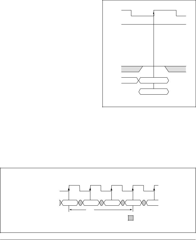
Before any READ or WRITE commands can be issued to a bank within the SDRAM, a row in that bank must be “opened.” This is accomplished via the ACTIVE command, which selects both the bank and the row to be activated (see Activating Specific Row Within Specific Bank).
After opening a row (issuing an ACTIVE command), a READ or WRITE command may be issued to that row, subject to the tRCD specification. Minimum tRCD should be divided by the clock period and rounded up to the next whole number to determine the earliest clock edge after the ACTIVE command on which a READ or WRITE command can be entered. For example, a tRCD specification of 20ns with a 125 MHz clock (8ns period) results in 2.5 clocks, rounded to 3. This is reflected in the following example, which covers any case where 2 < [tRCD (MIN)/tCK] ≤ 3. (The same procedure is used to convert other specification limits from time units to clock cycles).
A subsequent ACTIVE command to a different row in the same bank can only be issued after the previous active row has been “closed” (precharged). The minimum time interval between successive ACTIVE commands to the same bank is defined by tRC.
A subsequent ACTIVE command to another bank can be issued while the first bank is being accessed, which results in a reduction of total row-access overhead. The minimum time interval between successive ACTIVE commands to different banks is defined by tRRD.
Activating Specific Row Within Specific Bank
CLK
HIGH - Z
CKE
CS 

RAS 

CAS 

WE
A0-A10  ROW ADDRESS
BA0,BA1  BANK ADDRESS
Example: Meeting tRCD (MIN) when 2 < [tRCD (min)/tCK] ≤ 3
T0 |
T1 |
T2 |
T3 |
T4 |
CLK |
|
|
|
|
COMMAND ACTIVE |
NOP |
NOP |
READ or |
|
WRITE |
|
|||
|
tRCD |
|
|
|
|
|
|
DON'T CARE |
|
Integrated Silicon Solution, Inc. — 1-800-379-4774 |
15 |
TARGET SPECIFICATION Rev. 00A
07/01/01
IS42S32200A |
ISSI® |
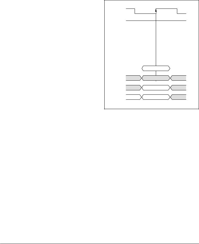
READS
READ bursts are initiated with a READ command, as shown in the READ COMMAND diagram.
The starting column and bank addresses are provided with the READ command, and auto precharge is either enabled or disabled for that burst access. If auto precharge is enabled, the row being accessed is precharged at the completion of the burst. For the generic READ commands used in the following illustrations, auto precharge is disabled.
During READ bursts, the valid data-out element from the starting column address will be available following the CAS latency after the READ command. Each subsequent data-out element will be valid by the next positive clock edge. The CAS Latency diagram shows general timing for each possible CAS latency setting.
Upon completion of a burst, assuming no other commands have been initiated, the DQs will go High-Z. A full-page burst will continue until terminated. (At the end of the page, it will wrap to column 0 and continue.)
Data from any READ burst may be truncated with a subsequent READ command, and data from a fixed-length READ burst may be immediately followed by data from a READ command. In either case, a continuous flow of data can be maintained. The first data element from the new burst follows either the last element of a completed burst or the last desired data element of a longer burst which is being truncated.
The new READ command should be issued x cycles before the clock edge at which the last desired data element is valid, where x equals the CAS latency minus one. This is shown in Consecutive READ Bursts for CAS latencies of two and three; data element n + 3 is either the last of a burst of four or the last desired of a longer burst. The 64Mb SDRAM uses a pipelined architecture and therefore does not require the 2n rule associated with a prefetch architecture. A READ command can be initiated on any clock cycle following a previous READ command. Full-speed random read accesses can be performed to the same bank, as shown in Random READ Accesses, or each subsequent READ may be performed to a different bank.
Data from any READ burst may be truncated with a subsequent WRITE command, and data from a fixed-length READ burst may be immediately followed by data from a WRITE command (subject to bus turnaround limitations). The WRITE burst may be initiated on the clock edge immediately following the last (or last desired) data element from the READ burst, provided that I/O contention can be avoided. In a given system design, there may be a possibility that the device driving the input data will go Low-Z before the SDRAM DQs go High-Z. In this case, at least a single-cycle delay should occur between the last read data and the WRITE command.
READ COMMAND
CLK
HIGH-Z
CKE
CS 

RAS 

CAS 

WE 

A0-A7  COLUMN ADDRESS
A8,A9
AUTO PRECHARGE
A10
NO PRECHARGE
BA0, BA1  BANK ADDRESS
The DQM input is used to avoid I/O contention, as shown in Figures RW1 and RW2. The DQM signal must be asserted (HIGH) at least two clocks prior to the WRITE command (DQM latency is two clocks for output buffers) to suppress data-out from the READ. Once the WRITE command is registered, the DQs will go High-Z (or remain High-Z), regardless of the state of the DQM signal, provided the DQM was active on the clock just prior to the WRITE command that truncated the READ command. If not, the second WRITE will be an invalid WRITE. For example, if DQM was LOW during T4 in Figure RW2, then the WRITEs at T5 and T7 would be valid, while the WRITE at T6 would be invalid.
The DQM signal must be de-asserted prior to the WRITE command (DQM latency is zero clocks for input buffers) to ensure that the written data is not masked. Figure RW1 shows the case where the clock frequency allows for bus contention to be avoided without adding a NOP cycle, and Figure RW2 shows the case where the additional NOP is needed.
A fixed-length READ burst may be followed by, or truncated with, a PRECHARGE command to the same bank (provided that auto precharge was not activated), and a full-page burst may be truncated with a PRECHARGE command to the
16 Integrated Silicon Solution, Inc. — 1-800-379-4774
TARGET SPECIFICATION Rev. 00A
07/01/01

IS42S32200A |
ISSI® |
same bank. The PRECHARGE command should be issued x cycles before the clock edge at which the last desired data element is valid, where x equals the CAS latency minus one. This is shown in the READ to PRECHARGE diagram for each possible CAS latency; data element n + 3 is either the last of a burst of four or the last desired of a longer burst. Following the PRECHARGE command, a subsequent command to the same bank cannot be issued until tRP is met. Note that part of the row precharge time is hidden during the access of the last data element(s).
In the case of a fixed-length burst being executed to completion, a PRECHARGE command issued at the optimum time (as described above) provides the same operation that would result from the same fixed-length burst with auto precharge. The disadvantage of the
PRECHARGE command is that it requires that the command and address buses be available at the appropriate time to issue the command; the advantage of the PRECHARGE command is that it can be used to truncate fixed-length or full-page bursts.
Full-page READ bursts can be truncated with the BURST TERMINATE command, and fixed-length READ bursts may be truncated with a BURST TERMINATE command, provided that auto precharge was not activated. The BURST TERMINATE command should be issued x cycles before the clock edge at which the last desired data element is valid, where x equals the CAS latency minus one. This is shown in the READ Burst Termination diagram for each possible CAS latency; data element n + 3 is the last desired data element of a longer burst.
CAS Latency
|
T0 |
T1 |
T2 |
T3 |
|
CLK |
|
|
|
|
|
COMMAND |
READ |
NOP |
NOP |
|
|
|
|
tAC |
|
|
|
DQ |
|
|
DOUT |
|
|
|
|
tLZ |
tOH |
|
|
|
|
CAS Latency - 2 |
|
|
|
|
T0 |
T1 |
T2 |
T3 |
T4 |
CLK |
|
|
|
|
|
COMMAND |
READ |
NOP |
NOP |
NOP |
|
|
|
|
|
tAC |
|
DQ |
|
|
|
DOUT |
|
|
|
|
tLZ |
|
tOH |
|
|
CAS Latency - 3 |
|
|
|
|
|
|
|
|
DON'T CARE |
|
|
|
|
|
UNDEFINED |
Integrated Silicon Solution, Inc. — 1-800-379-4774 |
17 |
TARGET SPECIFICATION Rev. 00A
07/01/01
 Loading...