


IS42S16128 |
ISSI® |
128K Words x 16 Bits x 2 Banks (4-MBIT) SYNCHRONOUS DYNAMIC RAM
FEBRUARY 2000
FEATURES |
|
|
|
|
|
|
|
DESCRIPTION |
|
|
|
|||||||||||
• Clock frequency: 125 MHz, 100 MHz, 83 MHz |
|
ISSI's 4Mb Synchronous DRAM IS42S16128 is organized as |
||||||||||||||||||||
• Two banks can be operated simultaneously and |
a 131072-word x 16-bit x 2-bank for improved performance. |
|||||||||||||||||||||
The synchronous DRAMs achieve high-speed data transfer |
||||||||||||||||||||||
|
independently |
|
|
|
|
|
|
|
||||||||||||||
|
|
|
|
|
|
|
|
using pipeline architecture. All inputs and outputs signals refer |
||||||||||||||
• Single 3.3V power supply |
|
|
||||||||||||||||||||
|
|
to the rising edge of the clock input. |
|
|
||||||||||||||||||
• |
LVTTL interface |
|
|
|
|
|
|
|
|
|
|
|
|
|
||||||||
• |
Programmable burst length |
|
|
|
PIN DESCRIPTIONS |
|
|
|||||||||||||||
|
– (1, 2, 4, 8, full page) |
|
|
|
|
|
|
|
|
|
|
|||||||||||
|
|
|
|
|
|
A0-A9 |
Address Input |
|
|
|||||||||||||
|
|
|
|
|
|
|
|
|
|
|
|
|
|
|
|
|
|
|
||||
• |
Programmable burst sequence: |
|
|
|
|
|
|
|
|
|||||||||||||
|
|
|
A0-A8 |
Row Address Input |
|
|
||||||||||||||||
|
Sequential/Interleave |
|
|
|
|
|
|
|
||||||||||||||
|
|
|
|
|
|
|
|
|
|
|
||||||||||||
|
|
|
|
|
|
A9 |
|
Bank Select Address |
|
|
||||||||||||
• Auto refresh, self refresh |
|
|
|
|
|
|
||||||||||||||||
|
|
|
|
|
|
|
|
|||||||||||||||
|
|
|
A0-A7 |
Column Address Input |
|
|
||||||||||||||||
• 1K refresh cycles every 16 ms |
|
|
|
|
|
|||||||||||||||||
|
|
|
|
|
|
|
|
|||||||||||||||
• Random column address every clock cycle |
|
|
|
I/O0 to I/O15 |
Data I/O |
|
|
|||||||||||||||
|
|
|
|
|
|
|
|
|||||||||||||||
• Programmable CAS latency (2, 3 clocks) |
|
|
|
CLK |
|
System Clock Input |
|
|
||||||||||||||
|
|
|
|
|
|
|
|
|||||||||||||||
• Burst read/write and burst read/single write |
|
|
|
CKE |
|
Clock Enable |
|
|
||||||||||||||
|
|
|
|
|
|
|
|
|||||||||||||||
|
operations capability |
|
|
|
|
|
CS |
|
Chip Select |
|
|
|||||||||||
• Byte controlled by LDQM and UDQM |
|
|
|
|
|
|
|
|||||||||||||||
|
|
|
RAS |
|
Row Address Strobe Command |
|||||||||||||||||
• Package 400-mil 50-pin TSOP II |
|
|
|
|
|
|
|
|||||||||||||||
|
|
|
CAS |
|
Column Address Strobe Command |
|||||||||||||||||
|
|
|
|
|
|
|
|
|
|
|
|
|
|
|
|
|
|
|
|
|
|
|
PIN CONFIGURATIONS |
|
|
|
WE |
|
Write Enable |
|
|
||||||||||||||
|
|
|
|
|
|
|
|
|||||||||||||||
|
|
|
LDQM |
Lower Bye, Input/Output Mask |
||||||||||||||||||
50-Pin TSOP (Type II) |
|
|
|
|
|
|||||||||||||||||
|
|
|
|
|
|
|
|
|
|
|||||||||||||
|
|
|
|
|
|
|
|
|
|
|
|
|
|
|
|
|
UDQM |
Upper Bye, Input/Output Mask |
||||
|
|
|
|
|
|
|
|
|
|
|
|
|
|
|
|
|||||||
|
|
|
|
|
|
|
|
|
|
|
|
|
|
|
|
|
|
|
|
|
|
|
|
VCC |
|
1 |
50 |
|
|
GND |
|
|
|
|
Vcc |
|
Power |
|
|
||||||
|
|
|
|
|
|
|
|
|
|
|||||||||||||
|
|
I/O0 |
|
49 |
|
|
I/O15 |
|
|
|
|
|
|
|
|
|
||||||
|
|
|
2 |
|
|
|
|
|
|
|
|
|
|
|
||||||||
|
|
|
|
|
|
|
|
|
GND |
|
Ground |
|
|
|||||||||
|
|
I/O1 |
|
48 |
|
|
I/O14 |
|
|
|
|
|
|
|
||||||||
|
|
|
3 |
|
|
|
|
|
|
|
|
|||||||||||
|
GNDQ |
|
47 |
|
|
GNDQ |
|
|
|
|
|
|
|
|
|
|||||||
|
|
4 |
|
|
|
|
|
|
VccQ |
Power Supply for I/O Pin |
|
|
||||||||||
|
|
|
|
|
|
|
|
|
46 |
|
|
|
|
|
|
|
|
|
||||
|
|
I/O2 |
5 |
|
|
I/O13 |
|
|
|
|
|
|
|
|
|
|||||||
|
|
I/O3 |
|
6 |
45 |
|
|
I/O12 |
|
|
|
|
GNDQ |
Ground for I/O Pin |
|
|
||||||
|
|
|
|
|
|
|
|
|
|
|
||||||||||||
|
|
|
|
|
|
|
|
|
||||||||||||||
|
VCCQ |
|
7 |
44 |
|
|
VCCQ |
|
|
|
|
|
|
|
|
|
||||||
|
|
|
|
|
|
|
|
NC |
|
No Connection |
|
|
||||||||||
|
|
I/O4 |
|
8 |
43 |
|
|
I/O11 |
|
|
|
|
|
|
|
|||||||
|
|
|
|
|
|
|
|
|
|
|
||||||||||||
|
|
I/O5 |
|
42 |
|
|
I/O10 |
|
|
|
|
|
|
|
|
|
||||||
|
|
|
9 |
|
|
|
|
|
|
|
|
|
|
|
||||||||
|
GNDQ |
|
41 |
|
|
GNDQ |
|
|
|
|
|
|
|
|
|
|||||||
|
|
10 |
|
|
|
|
|
|
|
|
|
|
|
|||||||||
|
|
I/O6 |
|
40 |
|
|
I/O9 |
|
|
|
|
|
|
|
|
|
||||||
|
|
|
11 |
|
|
|
|
|
|
|
|
|
|
|
||||||||
|
|
I/O7 |
|
39 |
|
|
I/O8 |
|
ORDERING INFORMATION |
|
|
|||||||||||
|
|
|
12 |
|
|
|
|
|
||||||||||||||
|
VCCQ |
|
13 |
38 |
|
|
VCCQ |
|
|
|
||||||||||||
|
|
|
|
|
|
|
||||||||||||||||
|
|
|
|
|
|
|
||||||||||||||||
|
LDQM |
|
14 |
37 |
|
|
NC |
|
Commercial Range: 0 C to 70 C |
|
|
|||||||||||
|
|
|
|
|
|
|
|
|
35 |
|
|
|
|
|
|
|||||||
|
|
CAS |
16 |
|
|
CLK |
|
|
|
|||||||||||||
|
|
WE |
15 |
36 |
|
|
UDQM |
|
|
|
|
|
|
|
|
|
||||||
|
|
|
|
|
|
|
|
|
|
|
|
|
|
|
|
|
|
|
|
|
||
|
|
|
|
|
|
|
|
|
|
|
|
|
|
|
|
|
|
|
|
|
|
|
|
|
|
|
|
|
|
|
|
34 |
|
|
|
|
|
Frequency |
Speed (ns) |
Order Part No. |
Package |
||||
|
|
|
|
|
|
|
|
|
|
|
||||||||||||
|
|
RAS |
|
17 |
|
|
CKE |
|
|
|||||||||||||
|
|
|
|
|
|
|
|
|
33 |
|
|
|
|
|
||||||||
|
|
|
CS |
|
18 |
|
|
NC |
|
|
|
|
|
|
|
|
|
|||||
|
|
|
|
|
|
|
|
|
125 MHz |
8 |
IS42S16128-8T |
400-mil TSOP II |
||||||||||
|
|
|
|
A9 |
|
19 |
32 |
|
|
NC |
|
|
|
|||||||||
|
|
|
|
|
|
|
||||||||||||||||
|
|
|
|
A8 |
|
20 |
31 |
|
|
NC |
|
|
|
|
|
|
|
|
|
|||
|
|
|
|
|
|
|
|
|
|
100 MHz |
10 |
IS42S16128-10T |
400-mil TSOP II |
|||||||||
|
|
|
|
A0 |
|
21 |
30 |
|
|
A7 |
|
|
|
|||||||||
|
|
|
|
|
|
|
|
|
|
|
|
|
|
|
|
|||||||
|
|
|
|
|
|
|
|
|
|
83 MHz |
12 |
IS42S16128-12T |
400-mil TSOP II |
|||||||||
|
|
|
|
A1 |
|
22 |
29 |
|
|
A6 |
|
|
|
|||||||||
|
|
|
|
|
|
|
||||||||||||||||
|
|
|
|
A2 |
|
23 |
28 |
|
|
A5 |
|
|
|
|
|
|
|
|
|
|||
|
|
|
|
|
|
|
|
|
|
|
|
|
|
|
|
|||||||
|
|
|
|
A3 |
|
24 |
27 |
|
|
A4 |
|
|
|
|
|
|
|
|
|
|||
|
|
|
|
|
|
|
|
|
|
|
|
|
|
|
|
|||||||
|
VCC |
|
26 |
|
|
GND |
|
|
|
|
|
|
|
|
|
|||||||
|
|
25 |
|
|
|
|
|
|
|
|
|
|
|
|||||||||
|
|
|
|
|
|
|
|
|
|
|
|
|
|
|
|
|
|
|
|
|
|
|
ISSI reserves the right to make changes to its products at any time without notice in order to improve design and supply the best possible product. We assume no responsibility for any errors which may appear in this publication. © Copyright 2000, Integrated Silicon Solution, Inc.
Integrated Silicon Solution, Inc. — 1-800-379-4774 |
1 |
Rev. A
03/13/00

IS42S16128 |
|
|
ISSI® |
|
PIN FUNCTIONS |
|
|
|
|
|
|
|
|
|
Pin No. |
Symbol |
Type |
Function (In Detail) |
|
|
|
|
|
|
20 to 24, |
A0-A8 |
Input Pin |
A0 to A8 are address inputs. A0-A8 are used as row address inputs during active |
|
27 to 30 |
|
|
command input and A0-A7 as column address inputs during read or write command |
|
|
|
|
input. A8 is also used to determine the precharge mode during other commands. If |
|
|
|
|
A8 is LOW during precharge command, the bank selected by A9 is precharged, but |
|
|
|
|
if A8 is HIGH, both banks will be precharged. |
|
|
|
|
When A8 is HIGH in read or write command cycle, the precharge starts automati- |
|
|
|
|
cally after the burst access. |
|
|
|
|
These signals become part of the OP CODE during mode register set command |
|
|
|
|
input. |
|
|
|
|
|
|
19 |
A9 |
Input Pin |
A9 is the bank selection signal. When A9 is LOW, bank 0 is selected and when high, |
|
|
|
|
bank 1 is selected. This signal becomes part of the OP CODE during mode register |
|
|
|
|
set command input. |
|
|
|
|
|
|
16 |
CAS |
Input Pin |
CAS, in conjunction with the RAS and WE, forms the device command. See the |
|
|
|
|
"Command Truth Table" item for details on device commands. |
|
|
|
|
|
|
34 |
CKE |
Input Pin |
The CKE input determines whether the CLK input is enabled within the device. |
|
|
|
|
When is CKE HIGH, the next rising edge of the CLK signal will be valid, and when |
|
|
|
|
LOW, invalid. When CKE is LOW, the device will be in either the power-down mode, |
|
|
|
|
the clock suspend mode, or the self refresh mode. The CKE is an asynchronous input. |
|
|
|
|
|
|
35 |
CLK |
Input Pin |
CLK is the master clock input for this device. Except for CKE, all inputs to this device |
|
|
|
|
are acquired in synchronization with the rising edge of this pin. |
|
|
|
|
|
|
18 |
CS |
Input Pin |
The CS input determines whether command input is enabled within the device. |
|
|
|
|
Command input is enabled when CS is LOW, and disabled with CS is HIGH. The |
|
|
|
|
device remains in the previous state when CS is HIGH. |
|
|
|
|
|
|
2, 3, 5, 6, 8, 9, 11 |
I/O0 to |
I/O Pin |
I/O0 to I/O15 are I/O pins. I/O through these pins can be controlled in byte units |
|
12, 39, 40, 42, 43, |
I/O15 |
|
using the LDQM and UDQM pins. |
|
45, 46, 48, 49 |
|
|
|
|
|
|
|
|
|
14, 36 |
LDQM, |
Input Pin |
LDQM and UDQM control the lower and upper bytes of the I/O buffers. In read |
|
|
UDQM |
|
mode, LDQM and UDQM control the output buffer. When LDQM or UDQM is LOW, |
|
|
|
|
the corresponding buffer byte is enabled, and when HIGH, disabled. The outputs go |
|
|
|
|
to the HIGH impedance state when LDQM/UDQM is HIGH. This function corre- |
|
|
|
|
sponds to OE in conventional DRAMs. In write mode, LDQM and UDQM control the |
|
|
|
|
input buffer. When LDQM or UDQM is LOW, the corresponding buffer byte is |
|
|
|
|
enabled, and data can be written to the device. When LDQM or UDQM is HIGH, |
|
|
|
|
input data is masked and cannot be written to the device. |
|
|
|
|
|
|
17 |
RAS |
Input Pin |
RAS, in conjunction with CAS and WE, forms the device command. See the |
|
|
|
|
"Command Truth Table" item for details on device commands. |
|
|
|
|
|
|
15 |
WE |
Input Pin |
WE, in conjunction with RAS and CAS, forms the device command. See the |
|
|
|
|
"Command Truth Table" item for details on device commands. |
|
|
|
|
|
|
7, 13, 38, 44 |
VCCQ |
Power Supply Pin |
VCCQ is the output buffer power supply. |
|
|
|
|
|
|
1, 25 |
VCC |
Power Supply Pin |
VCC is the device internal power supply. |
|
|
|
|
|
|
4, 10, 41, 47 |
GNDQ |
Power Supply Pin |
GNDQ is the output buffer ground. |
|
|
|
|
|
|
26, 50 |
GND |
Power Supply Pin |
GND is the device internal ground. |
|
|
|
|
|
|
2 Integrated Silicon Solution, Inc. — 1-800-379-4774
Rev. A
03/13/00
IS42S16128 |
ISSI® |
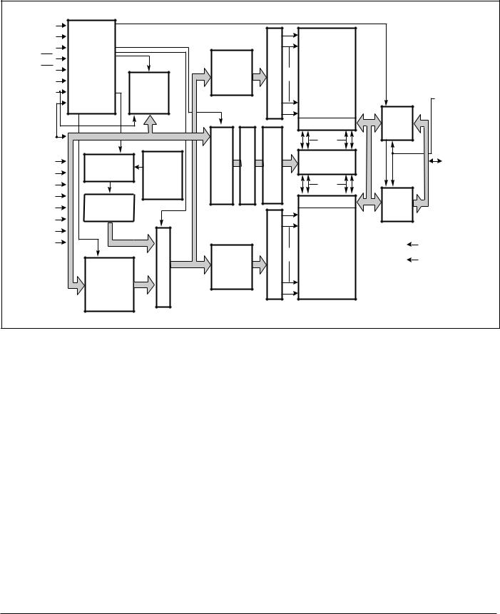
FUNCTIONAL BLOCK DIAGRAM
CLK |
|
|
|
|
|
|
|
|
|
|
|
|
CKE |
|
|
|
|
|
|
|
|
DECODER |
|
|
|
CS |
COMMAND |
|
|
|
|
|
|
MEMORY CELL |
|
|
||
RAS |
DECODER |
|
|
|
ROW |
|
|
|
|
|||
CAS |
|
& |
|
|
|
|
|
ARRAY |
|
|
||
|
|
|
ADDRESS |
|
|
|
|
|||||
WE |
CLOCK |
|
|
|
|
512 |
|
|
||||
MODE |
9 |
|
BUFFER |
|
|
BANK 0 |
|
|
||||
A9 |
GENERATOR |
|
|
9 |
ROW |
|
|
|||||
|
|
|
|
|
||||||||
REGISTER |
|
|
|
|
|
|
|
DQM |
||||
|
|
|
|
|
|
|
|
|
|
|||
|
|
|
9 |
|
|
|
|
|
|
SENSE AMP I/O GATE |
|
DATA IN |
|
|
|
|
|
|
|
|
|
|
|
BUFFER |
|
A8 |
|
|
|
|
|
ADDRESS LATCH |
BURST COUNTER |
|
ADDRESS BUFFER |
|
|
|
|
|
|
8 |
|
|
256x16 |
16 |
16 |
||||
|
|
|
|
COLUMN |
COLUMN |
|
|
|
||||
A7 |
|
REFRESH |
SELF |
|
COLUMN DECODER |
|
I/O 0-15 |
|||||
A6 |
|
CONTROLLER |
REFRESH |
|
8 |
|
|
|||||
|
CONTROLLER |
|
|
|
||||||||
A5 |
|
|
|
256x16 |
|
|
||||||
|
|
|
|
|
|
|||||||
A4 |
|
REFRESH |
|
|
SENSE AMP I/O GATE |
|
DATA OUT |
|||||
A3 |
|
|
|
|
|
|
|
|
|
BUFFER |
||
|
COUNTER |
|
|
|
|
|
|
|
|
|
||
A2 |
|
|
|
|
|
|
|
|
|
16 |
16 |
|
|
|
|
|
|
|
|
|
ROW DECODER |
|
|||
A1 |
|
|
|
|
|
|
|
|
MEMORY CELL |
|
|
|
A0 |
|
|
MULTIPLEXER |
|
|
|
|
|
|
Vcc/VccQ |
||
|
|
|
|
|
|
|
ARRAY |
|
||||
|
|
|
|
|
|
|
|
|
||||
|
|
|
|
|
ROW |
|
|
|
|
|||
|
|
|
|
|
|
|
512 |
|
GND/GNDQ |
|||
|
|
|
|
ADDRESS |
|
|
BANK 1 |
|
||||
|
|
ROW |
|
|
|
|
|
|||||
|
|
9 |
|
BUFFER |
|
9 |
|
|
|
|||
|
|
ADDRESS |
|
|
|
|
|
|||||
|
|
|
|
|
|
|
|
|
|
|||
|
9 |
LATCH |
|
|
|
|
|
|
|
|
||
|
|
|
|
|
|
|
|
|
|
|
||
Integrated Silicon Solution, Inc. — 1-800-379-4774 |
3 |
Rev. A
03/13/00

IS42S16128 |
|
|
|
ISSI® |
ABSOLUTE MAXIMUM RATINGS(1) |
|
|
|
|
|
|
|
|
|
Symbol |
Parameters |
Rating |
Unit |
|
|
|
|
|
|
VCC MAX |
Maximum Supply Voltage |
–1.0 to +4.6 |
V |
|
|
|
|
|
|
VccQ MAX |
Maximum Supply Voltage for Output Buffer |
–1.0 to +4.6 |
V |
|
|
|
|
|
|
VIN |
Input Voltage |
–1.0 to +5.5 |
V |
|
|
|
|
|
|
VOUT |
Output Voltage |
–1.0 to +4.6 |
V |
|
|
|
|
|
|
PD MAX |
Allowable Power Dissipation |
1 |
W |
|
|
|
|
|
|
ICS |
Output Shorted Current |
50 |
mA |
|
|
|
|
|
|
TOPR |
Operating Temperature |
0 to +70 |
°C |
|
|
|
|
|
|
TSTG |
Storage Temperature |
–55 to +150 |
°C |
|
|
|
|
|
|
DC RECOMMENDED OPERATING CONDITIONS
At TA = 0 to +70°C(2)
Symbol |
Parameter |
Min. |
Typ. |
Max. |
Unit |
VCC, VCCQ |
Supply Voltage |
3.0 |
3.3 |
3.6 |
V |
VIH |
Input High Voltage |
2.0 |
— |
5.5 |
V |
|
|
|
|
|
|
VIL |
Input Low Voltage |
–0.3 |
— |
+0.8 |
V |
|
|
|
|
|
|
Note:
1.Stress greater than those listed under ABSOLUTE MAXIMUM RATINGS may cause permanent damage to the device. This is a stress rating only and functional operation of the device at these or any other conditions above those indicated in the operational sections of this specification is not implied. Exposure to absolute maximum rating conditions for extended periods may affect reliability.
2.All voltages are referenced to GND.
3.VIH (max) = 5.5V for pulse width - 5 ns.
3. VIL (min) = –1.0V for pulse width - 5 ns.
CAPACITANCE CHARACTERISTICS
At TA = 0 to +25°C, Vcc = VccQ = 3.3 ± 0.3V, f = 1 MHz(1,2)
Symbol |
Parameter |
Typ. |
Max. |
Unit |
CIN1 |
Input Capacitance: A0-A9 |
— |
5 |
pF |
|
|
|
|
|
CIN2 |
Input Capacitance: (CLK, CKE, CS, RAS, CAS, WE, LDQM, UDQM) |
— |
5 |
pF |
|
|
|
|
|
CI/O |
Data Input/Output Capacitance: I/O0-I/O15 |
— |
7 |
pF |
|
|
|
|
|
4 Integrated Silicon Solution, Inc. — 1-800-379-4774
Rev. A
03/13/00

IS42S16128 |
|
|
|
|
|
ISSI® |
|||
DC ELECTRICAL CHARACTERISTICS |
|
|
|
|
|
|
|||
(Recommended Operation Conditions unless otherwise noted.) |
|
|
|
|
|
|
|||
|
|
|
|
|
|
|
|
|
|
Symbol |
Parameter |
Test Condition |
|
Speed |
Min. |
Max. |
Unit |
||
|
|
|
|
|
|
|
|
|
|
IIL |
Input Leakage Current |
0V ≤ VIN ≤ VCC, with pins other than |
|
–10 |
10 |
µA |
|||
|
|
the tested pin at 0V |
|
|
|
|
|
|
|
IOL |
Output Leakage Current |
Output is disabled |
|
|
–10 |
10 |
µA |
||
|
|
0V ≤ VOUT ≤ VCC |
|
|
|
|
|
|
|
VOH |
Output High Voltage Level |
IOUT = –2 mA |
|
|
2.4 |
— |
V |
||
|
|
|
|
|
|
|
|
|
|
VOL |
Output Low Voltage Level |
IOUT = +2 mA |
|
|
— |
0.4 |
V |
||
|
|
|
|
|
|
|
|
|
|
ICC1 |
Operating Current(1,2) |
One Bank Operation, Burst Length=1 |
|
— |
100 |
mA |
|||
|
|
tRC ≥ tRC (min.), IOUT = 0mA |
|
|
|
|
|
||
ICC2P |
Precharge Standby Current |
CKE ≤ VIL (MAX) |
tCK = tCK (MIN) |
— |
— |
3 |
mA |
||
ICC2PS |
(In Power-Down Mode) |
|
|
tCK = × |
— |
— |
2 |
mA |
|
ICC2N |
Precharge Standby Current |
CKE ≥ VIH (MIN) |
tCK = tCK (MIN) |
— |
— |
30 |
mA |
||
ICC2NS |
(In Non Power-Down Mode) |
|
|
tCK = × |
— |
— |
15 |
mA |
|
ICC3P |
Active Standby Current |
CKE ≤ VIL (MAX) |
tCK = tCK (MIN) |
— |
— |
3 |
mA |
||
ICC3PS |
(In Power-Down Mode) |
|
|
tCK = × |
— |
— |
2 |
mA |
|
ICC3N |
Active Standby Current |
CKE ≥ VIH (MIN) |
tCK = tCK (MIN) |
— |
— |
30 |
mA |
||
ICC3NS |
(In Non Power-Down Mode) |
|
|
tCK = × |
— |
— |
15 |
mA |
|
ICC4 |
Operating Current |
tCK = tCK (MIN) |
CAS latency = 3 |
-8 |
— |
160 |
mA |
||
|
(In Burst Mode)(1) |
IOUT = 0mA |
|
-10 |
— |
160 |
mA |
||
|
|
|
|
|
-12 |
— |
120 |
mA |
|
|
|
|
|
CAS latency = 2 |
-8 |
— |
120 |
mA |
|
|
|
|
|
|
-10 |
— |
120 |
mA |
|
|
|
|
|
|
-12 |
— |
110 |
mA |
|
|
|
|
|
|
|
|
|
|
|
ICC5 |
Auto-Refresh Current |
tRC = tRC (MIN) |
|
-8 |
— |
100 |
mA |
||
|
|
|
|
|
-10 |
— |
100 |
mA |
|
|
|
|
|
|
-12 |
— |
80 |
mA |
|
|
|
|
|
|
|
|
|
|
|
ICC6 |
Self-Refresh Current |
CKE ≤ 0.2V |
|
— |
— |
2 |
mA |
|
|
Notes:
1.These are the values at the minimum cycle time. Since the currents are transient, these values decrease as the cycle time increases. Also note that a bypass capacitor of at least 0.01 µF should be inserted between Vcc and GND for each memory chip to suppress power supply voltage noise (voltage drops) due to these transient currents.
2.Icc1 and Icc4 depend on the output load. The maximum values for Icc1 and Icc4 are obtained with the output open state.
Integrated Silicon Solution, Inc. — 1-800-379-4774 |
5 |
Rev. A
03/13/00

IS42S16128 |
|
|
|
|
|
|
ISSI® |
|||
AC CHARACTERISTICS(1,2,3) |
|
|
|
|
|
|
|
|
|
|
|
|
|
|
|
|
|
|
|
|
|
|
|
|
-8 |
|
-10 |
|
-12 |
|
|
|
Symbol |
Parameter |
|
Min. |
Max. |
Min. |
Max. |
Min. |
Max. |
Units |
|
|
|
|
|
|
|
|
|
|
|
|
tCK3 |
Clock Cycle Time |
CAS Latency = 3 |
8 |
— |
10 |
— |
12 |
— |
ns |
|
tCK2 |
|
CAS Latency = 2 |
13 |
— |
15 |
— |
17 |
— |
ns |
|
|
|
|
|
|
|
|
|
|
|
|
tAC3 |
Access Time From CLK(4) |
CAS Latency = 3 |
— |
6 |
— |
8 |
— |
10 |
ns |
|
tAC2 |
|
CAS Latency = 2 |
— |
10 |
— |
13 |
— |
15 |
ns |
|
|
|
|
|
|
|
|
|
|
|
|
tCHI |
CLK HIGH Level Width |
|
3 |
— |
4 |
— |
4.5 |
— |
ns |
|
|
|
|
|
|
|
|
|
|
|
|
tCL |
CLK LOW Level Width |
|
3 |
— |
4 |
— |
4.5 |
— |
ns |
|
|
|
|
|
|
|
|
|
|
|
|
tOH3 |
Output Data Hold Time |
CAS Latency = 3 |
3 |
— |
4 |
— |
4 |
— |
ns |
|
tOH2 |
|
CAS Latency = 2 |
3 |
— |
4 |
— |
4 |
— |
ns |
|
|
|
|
|
|
|
|
|
|
|
|
tLZ |
Output LOW Impedance Time |
|
0 |
— |
0 |
— |
0 |
— |
ns |
|
|
|
|
|
|
|
|
|
|
|
|
tHZ3 |
Output HIGH Impedance Time(5) |
CAS Latency = 3 |
3 |
6 |
4 |
8 |
4 |
10 |
ns |
|
tHZ2 |
|
CAS Latency = 2 |
3 |
10 |
4 |
12 |
4 |
14 |
ns |
|
|
|
|
|
|
|
|
|
|
|
|
tDS |
Input Data Setup Time |
|
2 |
— |
3 |
— |
3 |
— |
ns |
|
|
|
|
|
|
|
|
|
|
|
|
tDH |
Input Data Hold Time |
|
1 |
— |
1.5 |
— |
2 |
— |
ns |
|
|
|
|
|
|
|
|
|
|
|
|
tAS |
Address Setup Time |
|
2 |
— |
3 |
— |
3 |
— |
ns |
|
|
|
|
|
|
|
|
|
|
|
|
tAH |
Address Hold Time |
|
1 |
— |
1.5 |
— |
2 |
— |
ns |
|
|
|
|
|
|
|
|
|
|
|
|
tCKS |
CKE Setup Time |
|
2 |
— |
3 |
— |
3 |
— |
ns |
|
|
|
|
|
|
|
|
|
|
|
|
tCKH |
CKE Hold Time |
|
1 |
— |
1.5 |
— |
2 |
— |
ns |
|
|
|
|
|
|
|
|
|
|
|
|
tCKA |
CKE to CLK Recovery Delay Time |
|
1CLK+3 |
— |
1CLK+3 |
— |
1CLK+3 |
— |
ns |
|
|
|
|
|
|
|
|
|
|
|
|
tCS |
Command Setup Time (CS, RAS, CAS, WE, DQM) |
2 |
— |
3 |
— |
3 |
— |
ns |
||
|
|
|
|
|
|
|
|
|
|
|
tCH |
Command Hold Time (CS, RAS, CAS, WE, DQM) |
1 |
— |
1.5 |
— |
2 |
— |
ns |
||
|
|
|
|
|
|
|
|
|
|
|
tRC |
Command Period (REF to REF / ACT to ACT) |
80 |
— |
90 |
— |
108 |
— |
ns |
||
|
|
|
|
|
|
|
|
|
|
|
tRAS |
Command Period (ACT to PRE) |
|
54 |
12,000 |
60 |
12,000 |
72 |
12,000 |
ns |
|
|
|
|
|
|
|
|
|
|
|
|
tRP |
Command Period (PRE to ACT) |
|
24 |
— |
30 |
— |
34 |
— |
ns |
|
|
|
|
|
|
|
|
|
|
|
|
tRCD |
Active Command To Read / Write Command Delay Time |
24 |
— |
30 |
— |
34 |
— |
ns |
||
|
|
|
|
|
|
|
|
|
|
|
tRRD |
Command Period (ACT [0] to ACT[1]) |
|
24 |
— |
30 |
— |
34 |
— |
ns |
|
|
|
|
|
|
|
|
|
|
|
|
tDPL3 |
Input Data To Precharge |
CAS Latency = 3 |
1CLK+8 |
— |
1CLK+10 |
— |
1CLK+12 |
— |
ns |
|
|
Command Delay time |
|
|
|
|
|
|
|
|
|
tDPL2 |
|
CAS Latency = 2 |
8 |
— |
10 |
— |
12 |
— |
ns |
|
|
|
|
|
|
|
|
|
|
|
|
tDAL3 |
Input Data To Active / Refresh |
CAS Latency = 3 |
2CLK+24 |
— |
2CLK+30 |
— |
2CLK+34 |
— |
ns |
|
|
Command Delay time (During Auto-Precharge) |
|
|
|
|
|
|
|
|
|
tDAL2 |
|
CAS Latency = 2 |
1CLK+24 |
— |
1CLK+30 |
— |
1CLK+34 |
— |
ns |
|
|
|
|
|
|
|
|
|
|
|
|
tT |
|
Transition Time |
1 |
30 |
1 |
30 |
1 |
30 |
ns |
|
|
|
|
|
|
|
|
|
|
|
|
tREF |
Refresh Cycle Time |
|
— |
16 |
— |
16 |
— |
16 |
ms |
|
Notes:
1.When power is first applied, memory operation should be started 100 µs after Vcc and VccQ reach their stipulated voltages. Also note that the power-on sequence must be executed before starting memory operation.
2.Measured with tT = 1 ns.
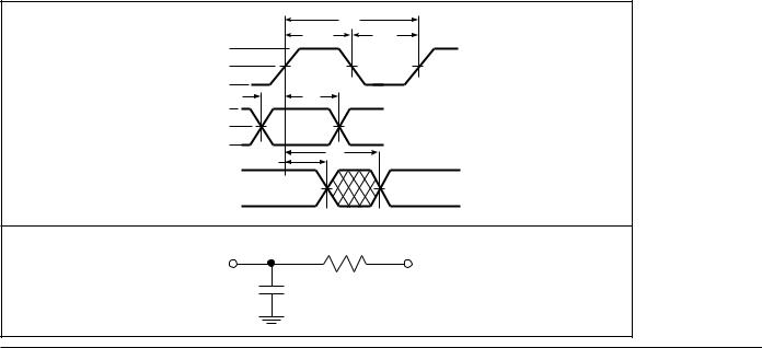
3.The reference level is 1.4 V when measuring input signal timing. Rise and fall times are measured between VIH (min.) and VIL (max.).
4.Access time is measured at 1.4V with the load shown in the figure below.
5.The time tHZ (max.) is defined as the time required for the output voltage to transition by ± 200 mV from VOH (min.) or VOL (max.) when the output is in the high impedance state.
6 Integrated Silicon Solution, Inc. — 1-800-379-4774
Rev. A
03/13/00
IS42S16128 |
|
|
|
|
|
|
|
ISSI® |
|||
OPERATING FREQUENCY / LATENCY RELATIONSHIPS |
|
|
|
|
|
|
|
||||
|
|
|
|
|
|
|
|
|
|
|
|
|
|
|
-8 |
|
|
-10 |
|
|
-12 |
|
|
Symbol |
Parameter |
Min. |
Typ. |
Max. |
Min. |
Typ. |
Max. |
Min. |
Typ. |
Max. |
Units |
|
|
|
|
|
|
|
|
|
|
|
|
— |
Clock Cycle Time |
8 |
10 |
25 |
10 |
15 |
30 |
12 |
17 |
34 |
ns |
|
|
|
|
|
|
|
|
|
|
|
|
— |
OperatingFrequency |
125 |
100 |
40 |
100 |
65 |
33 |
83 |
58 |
29 |
MHz |
|
|
|
|
|
|
|
|
|
|
|
|
tCAC |
CAS Latency |
3 |
2 |
1 |
3 |
2 |
1 |
3 |
2 |
1 |
cycle |
|
|
|
|
|
|
|
|
|
|
|
|
tRCD |
Active Command To Read/Write Command Delay Time |
3 |
2 |
1 |
3 |
2 |
1 |
3 |
2 |
1 |
cycle |
|
|
|
|
|
|
|
|
|
|
|
|
tRAC |
RAS Latency (tRCD + tCAC) |
6 |
4 |
2 |
6 |
4 |
2 |
6 |
4 |
2 |
cycle |
|
|
|
|
|
|
|
|
|
|
|
|
tRC |
Command Period (REF to REF / ACT to ACT) |
9 |
5 |
2 |
9 |
6 |
3 |
9 |
7 |
4 |
cycle |
|
|
|
|
|
|
|
|
|
|
|
|
tRAS |
Command Period (ACT to PRE) |
6 |
3 |
1 |
6 |
4 |
2 |
6 |
5 |
3 |
cycle |
|
|
|
|
|
|
|
|
|
|
|
|
tRP |
Command Period (PRE to ACT) |
3 |
2 |
1 |
3 |
2 |
1 |
3 |
2 |
1 |
cycle |
|
|
|
|
|
|
|
|
|
|
|
|
tRRD |
Command Period (ACT[0] to ACT [1]) |
3 |
2 |
1 |
3 |
2 |
1 |
3 |
2 |
1 |
cycle |
|
|
|
|
|
|
|
|
|
|
|
|
tCCD |
Column Command Delay Time |
1 |
1 |
1 |
1 |
1 |
1 |
1 |
1 |
1 |
cycle |
|
(READ, READA, WRIT, WRITA) |
|
|
|
|
|
|
|
|
|
|
|
|
|
|
|
|
|
|
|
|
|
|
tDPL |
Input Data To Precharge Command Delay Time |
1 |
1 |
1 |
1 |
1 |
1 |
1 |
1 |
1 |
cycle |
|
|
|
|
|
|
|
|
|
|
|
|
tDAL |
Input Data To Active/Refresh Command Delay Time |
4 |
3 |
2 |
4 |
3 |
2 |
4 |
3 |
2 |
cycle |
|
(DuringAuto-Precharge) |
|
|
|
|
|
|
|
|
|
|
|
|
|
|
|
|
|
|
|
|
|
|
tRBD |
Burst Stop Command To Output in HIGH-Z Delay Time |
3 |
2 |
1 |
3 |
2 |
1 |
3 |
2 |
1 |
cycle |
|
(Read) |
|
|
|
|
|
|
|
|
|
|
|
|
|
|
|
|
|
|
|
|
|
|
tWBD |
Burst Stop Command To Input in Invalid Delay Time |
0 |
0 |
0 |
0 |
0 |
0 |
0 |
0 |
0 |
cycle |
|
(Write) |
|
|
|
|
|
|
|
|
|
|
|
|
|
|
|
|
|
|
|
|
|
|
tRQL |
Precharge Command To Output in HIGH-Z Delay Time |
3 |
2 |
1 |
3 |
2 |
1 |
3 |
2 |
1 |
cycle |
|
(Read) |
|
|
|
|
|
|
|
|
|
|
|
|
|
|
|
|
|
|
|
|
|
|
tWDL |
Precharge Command To Input in Invalid Delay Time |
0 |
0 |
0 |
0 |
0 |
0 |
0 |
0 |
0 |
cycle |
|
(Write) |
|
|
|
|
|
|
|
|
|
|
|
|
|
|
|
|
|
|
|
|
|
|
tPQL |
Last Output To Auto-Precharge Start Time (Read) |
–2 |
–1 |
0 |
–2 |
–1 |
0 |
–2 |
–1 |
0 |
cycle |
|
|
|
|
|
|
|
|
|
|
|
|
tQMD |
DQM To Output Delay Time (Read) |
2 |
2 |
2 |
2 |
2 |
2 |
2 |
2 |
2 |
cycle |
|
|
|
|
|
|
|
|
|
|
|
|
tDMD |
DQM To Input Delay Time (Write) |
0 |
0 |
0 |
0 |
0 |
0 |
0 |
0 |
0 |
cycle |
|
|
|
|
|
|
|
|
|
|
|
|
tMCD |
Mode Register Set To Command Delay Time |
2 |
2 |
2 |
2 |
2 |
2 |
2 |
2 |
2 |
cycle |
|
|
|
|
|
|
|
|
|
|
|
|
AC TEST CONDITIONS (Input/Output Reference Level: 1.4V)
Input |
|
tCHI |
tCK |
|
|
tCL |
|
|
2.0V |
|
|
CLK |
1.4V |
|
|
|
0.8V |
|
|
|
tCS |
tCH |
|
|
2.0V |
|
|
INPUT |
1.4V |
|
|
|
0.8V |
|
tAC |
|
tOH |
|
|
|
|
|
|
OUTPUT |
|
1.4V |
1.4V |
Output Load |
|
|
500 Ω |
|
|
|
I/O |
+1.4V |
50 pF
Integrated Silicon Solution, Inc. — 1-800-379-4774 |
7 |
Rev. A
03/13/00
IS42S16128 |
|
|
ISSI® |
COMMANDS |
|
|
|
|
Active Command |
|
Read Command |
CLK |
|
CLK |
|
CKE |
HIGH |
CKE |
HIGH |
CS |
|
CS |
|
RAS |
|
RAS |
|
CAS |
|
CAS |
|
WE |
|
WE |
|
A0-A7 |
ROW |
A0-A7 |
COLUMN |
|
|
|
AUTO PRECHARGE |
A8 |
ROW |
A8 |
|
|
|
|
NO PRECHARGE |
|
BANK 1 |
|
BANK 1 |
A9 |
|
A9 |
|
|
BANK 0 |
|
BANK 0 |
|
Write Command |
|
Precharge Command |
CLK |
|
CLK |
|
CKE |
HIGH |
CKE |
HIGH |
CS |
|
CS |
|
RAS |
|
RAS |
|
CAS |
|
CAS |
|
WE |
|
WE |
|
A0-A7 |
COLUMN |
A0-A7 |
|
|
AUTO PRECHARGE |
|
BANK 0 AND BANK 1 |
A8 |
|
A8 |
|
|
NO PRECHARGE |
|
BANK 0 OR BANK 1 |
|
BANK 1 |
|
BANK 1 |
A9 |
|
A9 |
|
|
BANK 0 |
|
BANK 0 |
No-Operation Command |
Device Deselect Command |
||
CLK |
CLK |
CKE HIGH |
CKE HIGH |
CS |
CS |
RAS |
RAS |
CAS |
CAS |
WE |
WE |
A0-A7 |
A0-A7 |
A8 |
A8 |
A9 |
A9 |
Don't Care
8 Integrated Silicon Solution, Inc. — 1-800-379-4774
Rev. A
03/13/00

IS42S16128 |
|
|
ISSI® |
COMMANDS (cont.) |
|
|
|
Mode Register Set Command |
Auto-Refresh Command |
||
CLK |
|
CLK |
|
CKE |
HIGH |
CKE |
HIGH |
CS |
|
CS |
|
RAS |
|
RAS |
|
CAS |
|
CAS |
|
WE |
|
WE |
|
A0-A7 |
OP-CODE |
A0-A7 |
|
A8 |
OP-CODE |
A8 |
|
A9 |
OP-CODE |
A9 |
|
Self-Refresh Command |
Power Down Command |
||
CLK |
|
CLK |
|
CKE |
|
CKE ALL BANKS IDLE |
|
CS |
|
CS |
NOP |
RAS |
|
RAS |
NOP |
CAS |
|
CAS |
NOP |
WE |
|
WE |
NOP |
A0-A7 |
|
A0-A7 |
|
A8 |
|
A8 |
|
A9 |
|
A9 |
|
Clock Suspend Command |
Burst Stop Command |
||
CLK |
|
CLK |
|
CKE |
BANK(S) ACTIVE |
CKE |
HIGH |
CS |
NOP |
CS |
|
RAS |
NOP |
RAS |
|
CAS |
NOP |
CAS |
|
WE |
NOP |
WE |
|
A0-A7 |
|
A0-A7 |
|
A8 |
|
A8 |
|
A9 |
|
A9 |
Don't Care |
|
|
|
|
Integrated Silicon Solution, Inc. — 1-800-379-4774 |
|
9 |
|
Rev. A |
|
|
|
03/13/00

IS42S16128 |
ISSI® |
Mode Register Set Command
(CS, RAS, CAS, WE = LOW)
The IS42S16128 product incorporates a register that defines the device operating mode. This command functions as a data input pin that loads this register from the pins A0 to A9. When power is first applied, the stipulated power-on sequence should be executed and then the IS42S16128 should be initialized by executing a mode register set command.
Note that the mode register set command can be executed only when both banks are in the idle state, i.e.., deactivated.
Another command cannot be executed after a mode register set command until after the passage of the period tMCD, which is the period required for mode register set command execution.
Active Command
(CS, RAS = LOW, CAS, WE= HIGH)
The IS42S16128 includes two banks of 512 rows each. This command selects one of the two banks according to the A9 pin and activates the row selected by the pins A0 to A8.
This command corresponds to the fall of the RAS signal from HIGH to LOW in conventional DRAMs.
Read Command (cont.)
When the A8 pin is HIGH, this command functions as a read with auto-precharge command. After the burst read completes, the bank selected by pin A9 is precharged. When the A8 pin is LOW, the bank selected by the A9 pin remains in the activated state after the burst read completes.
Write Command
(CS, CAS, WE = LOW, RAS = HIGH)
When burst write mode has been selected with the mode register set command, this command selects the bank specified by the A9 pin and starts a burst write operation at the start address specified by pins A0 to A7. This first data must be input to the I/O pins in the cycle in which this command.
The selected bank must be activated before executing this command.
When A8 pin is HIGH, this command functions as a write with auto-precharge command. After the burst write completes, the bank selected by pin A9 is precharged. When the A8 pin is low, the bank selected by the A9 pin remains in the activated state after the burst write completes.
After the input of the last burst write data, the application must wait for the write recovery period (tDPL, tDAL) to elapse according to CAS latency.
Precharge Command
(CS, RAS, WE = LOW, CAS = HIGH)
This command starts precharging the bank selected by pins A8 and A9. When A8 is HIGH, both banks are precharged at the same time. When A8 is LOW, the bank selected by A9 is precharged. After executing this command, the next command for the selected bank(s) is executed after passage of the period tRP, which is the period required for bank precharging.
This command corresponds to the RAS signal from LOW to HIGH in conventional DRAMs
Read Command
(CS, CAS = LOW, RAS, WE = HIGH)
This command selects the bank specified by the A9 pin and starts a burst read operation at the start address specified by pins A0 to A7. Data is output following CAS latency.
The selected bank must be activated before executing this command.
Auto-Refresh Command
(CS, RAS, CAS = LOW, WE, CKE = HIGH)
This command executes the auto-refresh operation. The row address and bank to be refreshed are automatically generated during this operation.
Both banks must be placed in the idle state before executing this command.
The stipulated period (tRC) is required for a single refresh operation, and no other commands can be executed during this period.
The device goes to the idle state after the internal refresh operation completes.
This command must be executed at least 1024 times every 16 ms.
This command corresponds to CBR auto-refresh in conventional DRAMs.
10 Integrated Silicon Solution, Inc. — 1-800-379-4774
Rev. A
03/13/00
IS42S16128 |
ISSI® |
Self-Refresh Command
(CS, RAS, CAS, CKE = LOW, WE = HIGH)
This command executes the self-refresh operation. The row address to be refreshed, the bank, and the refresh interval are generated automatically internally during this operation. The self-refresh operation is started by dropping the CKE pin from HIGH to LOW. The self-refresh operation continues as long as the CKE pin remains LOW and there is no need for external control of any other pins. The self-refresh operation is terminated by raising the CKE pin from LOW to HIGH. The next command cannot be executed until the device internal recovery period (tRC) has elapsed. After the self-refresh, since it is impossible to determine the address of the last row to be refreshed, an auto-refresh should immediately be performed for all addresses (1024 cycles).
Both banks must be placed in the idle state before executing this command.
Burst Stop Command
(CS, WE, = LOW, RAS, CAS = HIGH)
The command forcibly terminates burst read and write operations. When this command is executed during a burst read operation, data output stops after the CAS latency period has elapsed.
No Operation
(CS, = LOW, RAS, CAS, WE = HIGH)
This command has no effect on the device.
Device Deselect Command
(CS = HIGH)
This command does not select the device for an object of operation. In other words, it performs no operation with respect to the device.
Power-Down Command
(CKE = LOW)
When both banks are in the idle (inactive) state, or when at least one of the banks is not in the idle (inactive) state, this command can be used to suppress device power dissipation by reducing device internal operations to the absolute minimum. Power-down mode is started by dropping the CKE pin from HIGH to LOW. Power-down mode continues as long as the CKE pin is held low.
Power-Down Command (cont.)
All pins other than the CKE pin are invalid and none of the other commands can be executed in this mode. The power-down operation is terminated by raising the CKE pin from LOW to HIGH. The next command cannot be executed until the recovery period (tCKA) has elapsed.
Since this command differs from the self-refresh command described above in that the refresh operation is not performed automatically internally, the refresh operation must be performed within the refresh period (tREF). Thus the maximum time that power-down mode can be held is just under the refresh cycle time.
Clock Suspend
(CKE = LOW)
This command can be used to stop the device internal clock temporarily during a read or write cycle. Clock suspend mode is started by dropping the CKE pin from HIGH to LOW. Clock suspend mode continues as long as the CKE pin is held LOW. All input pins other than the CKE pin are invalid and none of the other commands can be executed in this mode. Also note that the device internal state is maintained. Clock suspend mode is terminated by raising the CKE pin from LOW to HIGH, at which point device operation restarts. The next command cannot be executed until the recovery period (tCKA) has elapsed.
Since this command differs from the self-refresh command described above in that the refresh operation is not performed automatically internally, the refresh operation must be performed within the refresh period (tREF). Thus the maximum time that clock suspend mode can be held is just under the refresh cycle time.
Integrated Silicon Solution, Inc. — 1-800-379-4774 |
11 |
Rev. A
03/13/00
IS42S16128 |
|
|
|
|
|
|
|
|
|
|
ISSI® |
|||
COMMAND TRUTH TABLE(1,2) |
|
|
|
|
|
|
|
|
|
|
|
|
|
|
|
|
|
|
|
|
|
|
|
|
|
|
|
|
|
|
|
CKE |
|
|
|
|
|
|
|
|
|
|
|
|
Symbol |
Command |
n-1 |
n |
CS RAS |
CAS |
WE DQM |
A0 |
|
A8 |
A7-A0 |
I/On |
|||
|
|
|
|
|
|
|
|
|
|
|
|
|
||
MRS |
Mode Register Set(3,4) |
H |
X |
L |
L |
L |
L |
X |
|
OP CODE |
X |
|
||
REF |
Auto-Refresh(5) |
H |
H |
L |
L |
L |
H |
X |
X |
|
X |
X |
HIGH-Z |
|
SREF |
Self-Refresh(5,6) |
H |
L |
L |
L |
L |
H |
X |
X |
|
X |
X |
HIGH-Z |
|
PRE |
Precharge Selected Bank |
H |
X |
L |
L |
H |
L |
X |
BS |
|
L |
X |
X |
|
|
|
|
|
|
|
|
|
|
|
|
|
|
|
|
PALL |
Precharge Both Banks |
H |
X |
L |
L |
H |
L |
X |
X |
|
H |
X |
X |
|
|
|
|
|
|
|
|
|
|
|
|
|
|
|
|
ACT |
Bank Activate(7) |
H |
X |
L |
L |
H |
H |
X |
BS |
|
Row |
Row |
X |
|
WRIT |
Write |
H |
X |
L |
H |
L |
L |
X |
BS |
|
L |
Column |
X |
|
|
|
|
|
|
|
|
|
|
|
|
|
|
|
|
WRITA |
Write With Auto-Precharge(8) |
H |
X |
L |
H |
L |
L |
X |
BS |
|
H |
Column |
X |
|
READ |
Read(8) |
H |
X |
L |
H |
L |
H |
X |
BS |
|
L |
Column |
X |
|
READA |
Read With Auto-Precharge(8) |
H |
X |
L |
H |
L |
H |
X |
BS |
|
H |
Column |
X |
|
BST |
Burst Stop(9) |
H |
X |
L |
H |
H |
L |
X |
X |
|
X |
X |
X |
|
NOP |
No Operation |
H |
X |
L |
H |
H |
H |
X |
X |
|
X |
X |
X |
|
|
|
|
|
|
|
|
|
|
|
|
|
|
|
|
DESL |
Device Deselect |
H |
X |
H |
X |
X |
X |
X |
X |
|
X |
X |
X |
|
|
|
|
|
|
|
|
|
|
|
|
|
|
|
|
SBY |
Clock Suspend / Standby Mode |
L |
X |
X |
X |
X |
X |
X |
X |
|
X |
X |
X |
|
|
|
|
|
|
|
|
|
|
|
|
|
|
|
|
ENB |
Data Write / Output Enable |
H |
X |
X |
X |
X |
X |
L |
X |
|
X |
X |
Active |
|
|
|
|
|
|
|
|
|
|
|
|
|
|
|
|
MASK |
Data Mask / Output Disable |
H |
X |
X |
X |
X |
X |
H |
X |
|
X |
X |
HIGH-Z |
|
DQM TRUTH TABLE(1,2) |
|
|
|
|
|
|
|
|
|
|
|
|
|
|
|
|
|
|
|
|
|
|
|
|
|
|
|
|
|
|
|
CKE |
|
|
DQM |
|
|
|
|
|
|
|
|
|
Symbol |
Command |
n-1 |
n |
UPPER |
LOWER |
|
|
|
|
|
|
|
||
|
|
|
|
|
|
|
|
|
|
|
|
|
|
|
ENB |
Data Write / Output Enable |
H |
X |
|
L |
L |
|
|
|
|
|
|
|
|
|
|
|
|
|
|
|
|
|
|
|
|
|
|
|
MASK |
Data Mask / Output Disable |
H |
X |
|
H |
H |
|
|
|
|
|
|
|
|
|
|
|
|
|
|
|
|
|
|
|
|
|
|
|
ENBU |
Upper Byte Data Write / Output Enable |
H |
X |
|
L |
X |
|
|
|
|
|
|
|
|
|
|
|
|
|
|
|
|
|
|
|
|
|
|
|
ENBL |
Lower Byte Data Write / Output Enable |
H |
X |
|
X |
L |
|
|
|
|
|
|
|
|
|
|
|
|
|
|
|
|
|
|
|
|
|
|
|
MASKU |
Upper Byte Data Mask / Output Disable |
H |
X |
|
H |
X |
|
|
|
|
|
|
|
|
|
|
|
|
|
|
|
|
|
|
|
|
|
|
|
MASKL |
Lower Byte Data Mask / Output Disable |
H |
X |
|
X |
H |
|
|
|
|
|
|
|
|
CKE TRUTH TABLE(1,2) |
|
|
|
|
|
|
|
|
|
|
|
|
|
|
|
|
|
|
|
|
|
|
|
|
|
|
|
|
|
|
|
|
|
CKE |
|
|
|
|
|
|
|
|
|
|
Symbol |
Command |
Current State |
|
n-1 |
n |
CS |
RAS |
CAS |
WE |
A9 |
A8 A7-A0 |
|||
|
|
|
|
|
|
|
|
|
|
|
|
|
|
|
SPND |
Start Clock Suspend Mode |
Active |
|
H |
L |
X |
X |
|
X |
X |
X |
X |
X |
|
|
|
|
|
|
|
|
|
|
|
|
|
|
|
|
— |
Clock Suspend |
Other States |
|
L |
L |
X |
X |
|
X |
X |
X |
X |
X |
|
— |
Terminate Clock Suspend Mode |
Clock Suspend |
|
L |
H |
X |
X |
|
X |
X |
X |
X |
X |
|
|
|
|
|
|
|
|
|
|
|
|
|
|
|
|
REF |
Auto-Refresh |
Idle |
|
H |
H |
L |
L |
|
L |
H |
X |
X |
X |
|
|
|
|
|
|
|
|
|
|
|
|
|
|
|
|
SELF |
Start Self-Refresh Mode |
Idle |
|
H |
L |
L |
L |
|
L |
H |
X |
X |
X |
|
SELFX |
Terminate Self-Refresh Mode |
Self-Refresh |
|
L |
H |
L |
H |
|
H |
H |
X |
X |
X |
|
|
|
|
|
L |
H |
H |
X |
|
X |
X |
X |
X |
X |
|
|
|
|
|
|
|
|
|
|
|
|
|
|
|
|
PDWN |
Start Power-Down Mode |
Idle |
|
H |
L |
L |
H |
|
H |
H |
X |
X |
X |
|
|
|
|
|
H |
L |
H |
X |
|
X |
X |
X |
X |
X |
|
|
|
|
|
|
|
|
|
|
|
|
|
|
|
|
— |
Terminate Power-Down Mode |
Power-Down |
|
L |
H |
X |
X |
|
X |
X |
X |
X |
X |
|
|
|
|
|
|
|
|||||||||
|
|
|
|
|
|
|
|
|
|
|
|
|
|
|
12 |
|
|
|
Integrated Silicon Solution, Inc. — 1-800-379-4774 |
||||||||||
|
|
|
|
|
|
|
|
|
|
|
|
|
Rev. A |
|
|
|
|
|
|
|
|
|
|
|
|
|
|
03/13/00 |
|
IS42S16128 |
|
|
|
|
|
ISSI® |
||||
OPERATION COMMAND TABLE(1,2) |
|
|
|
|
|
|
|
|
||
Current State |
Command |
Operation |
CS |
RAS |
CAS |
WE |
A9 |
A8 |
A7-A0 |
|
|
|
|
|
|
|
|
|
|
|
|
Idle |
DESL |
No Operation or Power-Down(12) |
H |
X |
X |
X |
X |
X |
X |
|
|
NOP |
No Operation or Power-Down(12) |
L |
H |
H |
H |
X |
X |
X |
|
|
BST |
No Operation or Power-Down |
L |
H |
H |
L |
X |
X |
X |
|
|
READ / READA |
Illegal |
L |
H |
L |
H |
V |
V |
V |
|
|
WRIT/WRITA |
Illegal |
L |
H |
L |
L |
V |
V |
V |
|
|
ACT |
Row Active |
L |
L |
H |
H |
V |
V |
V |
|
|
PRE/PALL |
No Operation |
L |
L |
H |
L |
V |
V |
X |
|
|
REF/SELF |
Auto-Refresh or Self-Refresh(13) |
L |
L |
L |
H |
X |
X |
X |
|
|
MRS |
Mode Register Set |
L |
L |
L |
L |
|
OP CODE |
||
|
|
|
|
|
|
|
|
|
|
|
Row Active |
DESL |
No Operation |
H |
X |
X |
X |
X |
X |
X |
|
|
NOP |
No Operation |
L |
H |
H |
H |
X |
X |
X |
|
|
BST |
No Operation |
L |
H |
H |
L |
X |
X |
X |
|
|
READ/READA |
Read Start(17) |
L |
H |
L |
H |
V |
V |
V |
|
|
WRIT/WRITA |
Write Start(17) |
L |
H |
L |
L |
V |
V |
V |
|
|
ACT |
Illegal(10) |
L |
L |
H |
H |
V |
V |
V |
|
|
PRE/PALL |
Precharge(15) |
L |
L |
H |
L |
V |
V |
X |
|
|
REF/SELF |
Illegal |
L |
L |
L |
H |
X |
X |
X |
|
|
MRS |
Illegal |
L |
L |
L |
L |
|
OP CODE |
||
|
|
|
|
|
|
|
|
|
|
|
Read |
DESL |
Burst Read Continues, Row Active When Done |
H |
X |
X |
X |
X |
X |
X |
|
|
NOP |
Burst Read Continues, Row Active When Done |
L |
H |
H |
H |
X |
X |
X |
|
|
BST |
Burst Interrupted, Row Active After Interrupt |
L |
H |
H |
L |
X |
X |
X |
|
|
READ/READA |
Burst Interrupted, Read Restart After Interrupt(16) |
L |
H |
L |
H |
V |
V |
V |
|
|
WRIT/WRITA |
Burst Interrupted Write Start After Interrupt(11,16) |
L |
H |
L |
L |
V |
V |
V |
|
|
ACT |
Illegal(10) |
L |
L |
H |
H |
V |
V |
V |
|
|
PRE/PALL |
Burst Read Interrupted, Precharge After Interrupt |
L |
L |
H |
L |
V |
V |
X |
|
|
REF/SELF |
Illegal |
L |
L |
L |
H |
X |
X |
X |
|
|
MRS |
Illegal |
L |
L |
L |
L |
|
OP CODE |
||
|
|
|
|
|
|
|
|
|
|
|
Write |
DESL |
Burst Write Continues, Write Recovery When Done |
H |
X |
X |
X |
X |
X |
X |
|
|
NOP |
Burst Write Continues, Write Recovery When Done |
L |
H |
H |
H |
X |
X |
X |
|
|
BST |
Burst Write Interrupted, Row Active After Interrupt |
L |
H |
H |
L |
X |
X |
X |
|
|
READ/READA |
Burst Write Interrupted, Read Start After Interrupt(11,16) |
L |
H |
L |
H |
V |
V |
V |
|
|
WRIT/WRITA |
Burst Write Interrupted, Write Restart After Interrupt(16) |
L |
H |
L |
L |
V |
V |
V |
|
|
ACT |
Illegal(10) |
L |
L |
H |
H |
V |
V |
V |
|
|
PRE/PALL |
Burst Write Interrupted, Precharge After Interrupt |
L |
L |
H |
L |
V |
V |
X |
|
|
REF/SELF |
Illegal |
L |
L |
L |
H |
X |
X |
X |
|
|
MRS |
Illegal |
L |
L |
L |
L |
|
OP CODE |
||
|
|
|
|
|
|
|
|
|
|
|
Read With |
DESL |
Burst Read Continues, Precharge When Done |
H |
X |
X |
X |
X |
X |
X |
|
Auto- |
NOP |
Burst Read Continues, Precharge When Done |
L |
H |
H |
H |
X |
X |
X |
|
Precharge |
BST |
Illegal |
L |
H |
H |
L |
X |
X |
X |
|
|
READ/READA |
Illegal |
L |
H |
L |
H |
V |
V |
V |
|
|
WRIT/WRITA |
Illegal |
L |
H |
L |
L |
V |
V |
V |
|
|
ACT |
Illegal(10) |
L |
L |
H |
H |
V |
V |
V |
|
|
PRE/PALL |
Illegal(10) |
L |
L |
H |
L |
V |
V |
X |
|
|
REF/SELF |
Illegal |
L |
L |
L |
H |
X |
X |
X |
|
|
MRS |
Illegal |
L |
L |
L |
L |
|
OP CODE |
||
|
|
|
|
|
|
|
|
|
||
|
|
|
|
|
|
|
|
|
|
|
Integrated Silicon Solution, Inc. — 1-800-379-4774 |
|
|
|
|
|
|
13 |
|
||
Rev. A |
|
|
|
|
|
|
|
|
|
|
03/13/00

IS42S16128 |
|
|
|
|
|
ISSI® |
||||
OPERATION COMMAND TABLE(1,2) |
|
|
|
|
|
|
|
|
||
Current State |
Command |
Operation |
CS |
RAS |
CAS |
WE |
A9 |
A8 |
A7-A0 |
|
|
|
|
|
|
|
|
|
|
|
|
Write With |
DESL |
Burst Write Continues, Write Recovery And Precharge |
H |
X |
X |
X |
X |
X |
X |
|
Auto-Precharge |
|
When Done |
|
|
|
|
|
|
|
|
|
NOP |
Burst Write Continues, Write Recovery And Precharge |
L |
H |
H |
H |
X |
X |
X |
|
|
BST |
Illegal |
L |
H |
H |
L |
X |
X |
X |
|
|
READ/READA |
Illegal |
L |
H |
L |
H |
V |
V |
V |
|
|
WRIT/WRITA |
Illegal |
L |
H |
L |
L |
V |
V |
V |
|
|
ACT |
Illegal(10) |
L |
L |
H |
H |
V |
V |
V |
|
|
PRE/PALL |
Illegal(10) |
L |
L |
H |
L |
V |
V |
X |
|
|
REF/SELF |
Illegal |
L |
L |
L |
H |
X |
X |
X |
|
|
MRS |
Illegal |
L |
L |
L |
L |
|
OPCODE |
||
|
|
|
|
|
|
|
|
|
|
|
Row Precharge |
DESL |
No Operation, Idle State After tRP Has Elapsed |
H |
X |
X |
X |
X |
X |
X |
|
|
NOP |
No Operation, Idle State After tRP Has Elapsed |
L |
H |
H |
H |
X |
X |
X |
|
|
BST |
No Operation, Idle State After tRP Has Elapsed |
L |
H |
H |
L |
X |
X |
X |
|
|
READ/READA |
Illegal(10) |
L |
H |
L |
H |
V |
V |
V |
|
|
WRIT/WRITA |
Illegal(10) |
L |
H |
L |
L |
V |
V |
V |
|
|
ACT |
Illegal(10) |
L |
L |
H |
H |
V |
V |
V |
|
|
PRE/PALL |
No Operation, Idle State After tRP Has Elapsed(10) |
L |
L |
H |
L |
V |
V |
X |
|
|
REF/SELF |
Illegal |
L |
L |
L |
H |
X |
X |
X |
|
|
MRS |
Illegal |
L |
L |
L |
L |
|
OP CODE |
||
|
|
|
|
|
|
|
|
|
|
|
Immediately |
DESL |
No Operation, Row Active After tRCD Has Elapsed |
H |
X |
X |
X |
X |
X |
X |
|
Following |
NOP |
No Operation, Row Active After tRCD Has Elapsed |
L |
H |
H |
H |
X |
X |
X |
|
Row Active |
BST |
No Operation, Row Active After tRCD Has Elapsed |
L |
H |
H |
L |
X |
X |
X |
|
|
READ/READA |
Illegal(10) |
L |
H |
L |
H |
V |
V |
V |
|
|
WRIT/WRITA |
Illegal(10) |
L |
H |
L |
L |
V |
V |
V |
|
|
ACT |
Illegal(10,14) |
L |
L |
H |
H |
V |
V |
V |
|
|
PRE/PALL |
Illegal(10) |
L |
L |
H |
L |
V |
V |
X |
|
|
REF/SELF |
Illegal |
L |
L |
L |
H |
X |
X |
X |
|
|
MRS |
Illegal |
L |
L |
L |
L |
|
OP CODE |
||
|
|
|
|
|
|
|
|
|
|
|
Write |
DESL |
No Operation, Row Active After tDPL Has Elapsed |
H |
X |
X |
X |
X |
X |
X |
|
Recovery |
NOP |
No Operation, Row Active After tDPL Has Elapsed |
L |
H |
H |
H |
X |
X |
X |
|
|
BST |
No Operation, Row Active After tDPL Has Elapsed |
L |
H |
H |
L |
X |
X |
X |
|
|
READ/READA |
Read Start |
L |
H |
L |
H |
V |
V |
V |
|
|
WRIT/WRITA |
Write Restart |
L |
H |
L |
L |
V |
V |
V |
|
|
ACT |
Illegal(10) |
L |
L |
H |
H |
V |
V |
V |
|
|
PRE/PALL |
Illegal(10) |
L |
L |
H |
L |
V |
V |
X |
|
|
REF/SELF |
Illegal |
L |
L |
L |
H |
X |
X |
X |
|
|
MRS |
Illegal |
L |
L |
L |
L |
|
OP CODE |
||
|
|
|
|
|
|
|
|
|
|
|
14 Integrated Silicon Solution, Inc. — 1-800-379-4774
Rev. A
03/13/00

IS42S16128 |
|
|
|
|
|
ISSI® |
||||
OPERATION COMMAND TABLE(1,2) |
|
|
|
|
|
|
|
|
||
Current State |
Command |
Operation |
CS |
RAS |
CAS |
WE |
A9 |
A8 |
A7-A0 |
|
|
|
|
|
|
|
|
|
|
|
|
Write Recovery |
DESL |
No Operation, Idle State After tDAL Has Elapsed |
H |
X |
X |
X |
X |
X |
X |
|
With Auto- |
NOP |
No Operation, Idle State After tDAL Has Elapsed |
L |
H |
H |
H |
X |
X |
X |
|
Precharge |
BST |
No Operation, Idle State After tDAL Has Elapsed |
L |
H |
H |
L |
X |
X |
X |
|
|
READ/READA |
Illegal(10) |
L |
H |
L |
H |
V |
V |
V |
|
|
WRIT/WRITA |
Illegal(10) |
L |
H |
L |
L |
V |
V |
V |
|
|
ACT |
Illegal(10) |
L |
L |
H |
H |
V |
V |
V |
|
|
PRE/PALL |
Illegal(10) |
L |
L |
H |
L |
V |
V |
X |
|
|
REF/SELF |
Illegal |
L |
L |
L |
H |
X |
X |
X |
|
|
MRS |
Illegal |
L |
L |
L |
L |
|
OP CODE |
||
|
|
|
|
|
|
|
|
|
|
|
Refresh |
DESL |
No Operation, Idle State After tRP Has Elapsed |
H |
X |
X |
X |
X |
X |
X |
|
|
NOP |
No Operation, Idle State After tRP Has Elapsed |
L |
H |
H |
H |
X |
X |
X |
|
|
BST |
No Operation, Idle State After tRP Has Elapsed |
L |
H |
H |
L |
X |
X |
X |
|
|
READ/READA |
Illegal |
L |
H |
L |
H |
V |
V |
V |
|
|
WRIT/WRITA |
Illegal |
L |
H |
L |
L |
V |
V |
V |
|
|
ACT |
Illegal |
L |
L |
H |
H |
V |
V |
V |
|
|
PRE/PALL |
Illegal |
L |
L |
H |
L |
V |
V |
X |
|
|
REF/SELF |
Illegal |
L |
L |
L |
H |
X |
X |
X |
|
|
MRS |
Illegal |
L |
L |
L |
L |
|
OP CODE |
||
|
|
|
|
|
|
|
|
|
|
|
Mode Register |
DESL |
No Operation, Idle State After tMCD Has Elapsed |
H |
X |
X |
X |
X |
X |
X |
|
Set |
NOP |
No Operation, Idle State After tMCD Has Elapsed |
L |
H |
H |
H |
X |
X |
X |
|
|
BST |
No Operation, Idle State After tMCD Has Elapsed |
L |
H |
H |
L |
X |
X |
X |
|
|
READ/READA |
Illegal |
L |
H |
L |
H |
V |
V |
V |
|
|
WRIT/WRITA |
Illegal |
L |
H |
L |
L |
V |
V |
V |
|
|
ACT |
Illegal |
L |
L |
H |
H |
V |
V |
V |
|
|
PRE/PALL |
Illegal |
L |
L |
H |
L |
V |
V |
X |
|
|
REF/SELF |
Illegal |
L |
L |
L |
H |
X |
X |
X |
|
|
MRS |
Illegal |
L |
L |
L |
L |
|
OP CODE |
||
|
|
|
|
|
|
|
|
|
|
|
Notes:
1.H: HIGH level input, L: LOW level input, X: HIGH or LOW level input, V: Valid data input
2.All input signals are latched on the rising edge of the CLK signal.
3.Both banks must be placed in the inactive (idle) state in advance.
4.The state of the A0 to A9 pins is loaded into the mode register as an OP code.
5.The row address is generated automatically internally at this time. The I/O pin and the address pin data is ignored.
6.During a self-refresh operation, all pin data (states) other than CKE is ignored.
7.The selected bank must be placed in the inactive (idle) state in advance.
8.The selected bank must be placed in the active state in advance.
9.This command is valid only when the burst length set to full page.
10.This is possible depending on the state of the bank selected by the A9 pin.
11.Time to switch internal busses is required.
12.The IS42S16128 can be switched to power-down mode by dropping the CKE pin LOW when both banks in the idle state. Input pins other than CKE are ignored at this time.
13.The IS42S16128 can be switched to self-refresh mode by dropping the CKE pin LOW when both banks in the idle state. Input pins other than CKE are ignored at this time.
14.Possible if tRRD is satisfied.
15.Illegal if tRAS is not satisfied.
16.The conditions for burst interruption must be observed. Also note that the IS42S16128 will enter the precharged state immediately after the burst operation completes if auto-precharge is selected.
17.Command input becomes possible after the period tRCD has elapsed. Also note that the IS42S16128 will enter the precharged state immediately after the burst operation completes if auto-precharge is selected.
Integrated Silicon Solution, Inc. — 1-800-379-4774 |
15 |
Rev. A
03/13/00

IS42S16128 |
|
|
|
|
|
|
|
ISSI® |
|||
CKE RELATED COMMAND TRUTH TABLE(1) |
|
|
|
|
|
|
|
|
|
|
|
|
|
CKE |
|
|
|
|
|
|
|
|
|
Current State |
Operation |
n-1 |
n |
CS |
RAS |
CAS |
WE |
A9 |
A8 |
A7-A0 |
|
|
|
|
|
|
|
|
|
|
|
|
|
Self-Refresh |
Undefined |
H |
X |
X |
X |
X |
X |
X |
X |
X |
|
|
Self-Refresh Recovery(2) |
L |
H |
H |
X |
X |
X |
X |
X |
X |
|
|
Self-Refresh Recovery(2) |
L |
H |
L |
H |
H |
X |
X |
X |
X |
|
|
Illegal(2) |
L |
H |
L |
H |
L |
X |
X |
X |
X |
|
|
Illegal(2) |
L |
H |
L |
L |
X |
X |
X |
X |
X |
|
|
Self-Refresh |
L |
L |
X |
X |
X |
X |
X |
X |
X |
|
|
|
|
|
|
|
|
|
|
|
|
|
Self-Refresh Recovery |
Idle State After tRC Has Elapsed |
H |
H |
H |
X |
X |
X |
X |
X |
X |
|
|
Idle State After tRC Has Elapsed |
H |
H |
L |
H |
H |
X |
X |
X |
X |
|
|
Illegal |
H |
H |
L |
H |
L |
X |
X |
X |
X |
|
|
Illegal |
H |
H |
L |
L |
X |
X |
X |
X |
X |
|
|
Power-Down on the Next Cycle |
H |
L |
H |
X |
X |
X |
X |
X |
X |
|
|
Power-Down on the Next Cycle |
H |
L |
L |
H |
H |
X |
X |
X |
X |
|
|
Illegal |
H |
L |
L |
H |
L |
X |
X |
X |
X |
|
|
Illegal |
H |
L |
L |
L |
X |
X |
X |
X |
X |
|
|
Clock Suspend Termination on the Next Cycle (2) |
L |
H |
X |
X |
X |
X |
X |
X |
X |
|
|
Clock Suspend |
L |
L |
X |
X |
X |
X |
X |
X |
X |
|
|
|
|
|
|
|
|
|
|
|
|
|
Power-Down |
Undefined |
H |
X |
X |
X |
X |
X |
X |
X |
X |
|
|
Power-Down Mode Termination, Idle After |
L |
H |
X |
X |
X |
X |
X |
X |
X |
|
|
That Termination(2) |
|
|
|
|
|
|
|
|
|
|
|
Power-Down Mode |
L |
L |
X |
X |
X |
X |
X |
X |
X |
|
|
|
|
|
|
|
|
|
|
|
|
|
Both Banks Idle |
No Operation |
H |
H |
H |
X |
X |
X |
X |
X |
X |
|
|
See the Operation Command Table |
H |
H |
L |
H |
X |
X |
X |
X |
X |
|
|
Bank Active Or Precharge |
H |
H |
L |
L |
H |
X |
X |
X |
X |
|
|
Auto-Refresh |
H |
H |
L |
L |
L |
H |
X |
X |
X |
|
|
Mode Register Set |
H |
H |
L |
L |
L |
L |
|
OP CODE |
||
|
See the Operation Command Table |
H |
L |
H |
X |
X |
X |
X |
X |
X |
|
|
See the Operation Command Table |
H |
L |
L |
H |
X |
X |
X |
X |
X |
|
|
See the Operation Command Table |
H |
L |
L |
L |
H |
X |
X |
X |
X |
|
|
Self-Refresh(3) |
H |
L |
L |
L |
L |
H |
X |
X |
X |
|
|
See the Operation Command Table |
H |
L |
L |
L |
L |
L |
|
OP CODE |
||
|
Power-Down Mode(3) |
L |
X |
X |
X |
X |
X |
X |
X |
X |
|
Other States |
See the Operation Command Table |
H |
H |
X |
X |
X |
X |
X |
X |
X |
|
|
Clock Suspend on the Next Cycle(4) |
H |
L |
X |
X |
X |
X |
X |
X |
X |
|
|
Clock Suspend Termination on the Next Cycle |
L |
H |
X |
X |
X |
X |
X |
X |
X |
|
|
Clock Suspend Termination on the Next Cycle |
L |
L |
X |
X |
X |
X |
X |
X |
X |
|
|
|
|
|
|
|
|
|
|
|
|
|
Notes:
1.H: HIGH level input, L: LOW level input, X: HIGH or LOW level input
2.The CLK pin and the other input are reactivated asynchronously by the transition of the CKE level from LOW to HIGH. The minimum setup time (tCKA) required before all commands other than mode termination must be satisfied.
3.Both banks must be set to the inactive (idle) state in advance to switch to power-down mode or self-refresh mode.
4.The input must be command defined in the operation command table.
16 Integrated Silicon Solution, Inc. — 1-800-379-4774
Rev. A
03/13/00

IS42S16128 |
|
|
|
|
|
|
|
|
|
|
|
ISSI® |
TWO BANKS OPERATION COMMAND TRUTH TABLE(1,2) |
|
|
|
|
||||||||
|
|
|
|
|
|
|
|
Previous State |
Next State |
|||
Operation |
CS |
RAS |
CAS |
WE |
A9 |
A8 |
A7-A0 |
BANK0 |
BANK1 |
BANK0 |
BANK1 |
|
|
|
|
|
|
|
|
|
|
|
|
|
|
DESL |
H |
X |
X |
X |
X |
X |
X |
Any |
Any |
Any |
Any |
|
|
|
|
|
|
|
|
|
|
|
|
|
|
NOP |
L |
H |
H |
H |
X |
X |
X |
Any |
Any |
Any |
Any |
|
|
|
|
|
|
|
|
|
|
|
|
|
|
BST |
L |
H |
H |
L |
X |
X |
X |
R/W/A |
I/A |
A |
I/A |
|
|
|
|
|
|
|
|
|
I |
I/A |
I |
I/A |
|
|
|
|
|
|
|
|
|
I/A |
R/W/A |
I/A |
A |
|
|
|
|
|
|
|
|
|
I/A |
I |
I/A |
I |
|
|
|
|
|
|
|
|
|
|
|
|
|
|
READ/READA |
L |
H |
L |
H |
H |
H |
CA |
I/A |
R/W/A |
I/A |
RP |
|
|
|
|
|
|
H |
H |
CA |
R/W |
A |
A |
RP |
|
|
|
|
|
|
H |
L |
CA |
I/A |
R/W/A |
I/A |
R |
|
|
|
|
|
|
H |
L |
CA |
R/W |
A |
A |
R |
|
|
|
|
|
|
L |
H |
CA |
R/W/A |
I/A |
RP |
I/A |
|
|
|
|
|
|
L |
H |
CA |
A |
R/W |
RP |
A |
|
|
|
|
|
|
L |
L |
CA |
R/W/A |
I/A |
R |
I/A |
|
|
|
|
|
|
L |
L |
CA |
A |
R/W |
R |
A |
|
|
|
|
|
|
|
|
|
|
|
|
|
|
WRIT/WRITA |
L |
H |
L |
L |
H |
H |
CA |
I/A |
R/W/A |
I/A |
WP |
|
|
|
|
|
|
H |
H |
CA |
R/W |
A |
A |
WP |
|
|
|
|
|
|
H |
L |
CA |
I/A |
R/W/A |
I/A |
W |
|
|
|
|
|
|
H |
L |
CA |
R/W |
A |
A |
W |
|
|
|
|
|
|
L |
H |
CA |
R/W/A |
I/A |
WP |
I/A |
|
|
|
|
|
|
L |
H |
CA |
A |
R/W |
WP |
A |
|
|
|
|
|
|
L |
L |
CA |
R/W/A |
I/A |
W |
I/A |
|
|
|
|
|
|
L |
L |
CA |
A |
R/W |
W |
A |
|
|
|
|
|
|
|
|
|
|
|
|
|
|
ACT |
L |
L |
H |
H |
H |
RA |
RA |
Any |
I |
Any |
A |
|
|
|
|
|
|
L |
RA |
RA |
I |
Any |
A |
Any |
|
|
|
|
|
|
|
|
|
|
|
|
|
|
PRE/PALL |
L |
L |
H |
L |
X |
H |
X |
R/W/A/I |
I/A |
I |
I |
|
|
|
|
|
|
X |
H |
X |
I/A |
R/W/A/I |
I |
I |
|
|
|
|
|
|
H |
L |
X |
I/A |
R/W/A/I |
I/A |
I |
|
|
|
|
|
|
H |
L |
X |
R/W/A/I |
I/A |
R/W/A/I |
I |
|
|
|
|
|
|
L |
L |
X |
R/W/A/I |
I/A |
I |
I/A |
|
|
|
|
|
|
L |
L |
X |
I/A |
R/W/A/I |
I |
R/W/A/I |
|
|
|
|
|
|
|
|
|
|
|
|
|
|
REF |
L |
L |
L |
H |
X |
X |
X |
I |
I |
I |
I |
|
|
|
|
|
|
|
|
|
|
|
|
|
|
MRS |
L |
L |
L |
L |
|
OPCODE |
I |
I |
I |
I |
||
|
|
|
|
|
|
|
|
|
|
|
|
|
Notes:
1.H: HIGH level input, L: LOW level input, X: HIGH or LOW level input, RA: Row Address, CA: Column Address
2.The device state symbols are interpreted as follows:
I |
Idle (inactive state) |
A |
Row Active State |
R |
Read |
W |
Write |
RP |
Read With Auto-Precharge |
WP |
Write With Auto-Precharge |
Any |
Any State |
Integrated Silicon Solution, Inc. — 1-800-379-4774 |
17 |
Rev. A
03/13/00
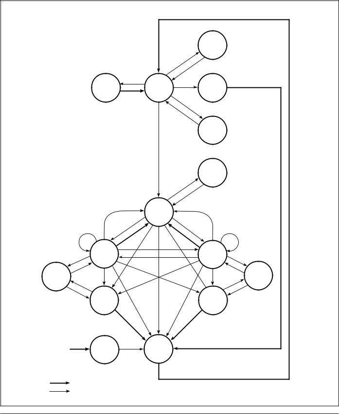
IS42S16128 |
ISSI® |
SIMPLIFIED STATE TRANSITION DIAGRAM (One Bank Operation) |
|
|
|
|
|
|
SELF |
|
|
|
|
|
|
|
REFRESH |
|
|
|
|
|
|
SREF entry |
|
|
|
|
|
|
|
SREF exit |
|
|
|
|
|
MODE |
MRS |
REF |
AUTO |
|
|
|
|
REGISTER |
|
|
|||
|
|
IDLE |
REFRESH |
|
|
||
|
|
SET |
|
|
|
|
|
|
|
|
|
|
|
|
|
|
|
|
|
CKE_ |
|
|
|
|
|
|
|
CKE |
|
|
|
|
|
|
|
ACT |
IDLE |
|
|
|
|
|
|
POWER |
|
|
|
|
|
|
|
|
|
|
|
|
|
|
|
|
DOWN |
|
|
|
|
|
|
|
ACTIVE |
|
|
|
|
|
|
|
POWER |
|
|
|
|
|
|
|
DOWN |
|
|
|
|
|
|
CKE_ |
|
|
|
|
|
|
|
CKE |
|
|
|
|
|
BST |
|
BANK |
BST |
|
|
|
|
|
ACTIVE |
|
|
||
|
|
|
|
|
|
|
|
|
|
|
WRIT |
READ |
|
|
|
|
WRIT |
|
|
|
|
READ |
|
|
|
|
WRITA |
READA |
|
|
|
|
|
|
READ |
|
|
|
|
|
CKE_ |
WRITE |
|
|
READ |
CKE_ |
|
|
|
|
WRIT |
|
|
||
|
|
|
|
|
|
|
|
CLOCK |
CKE |
|
|
READA |
CKE |
CLOCK |
|
|
WRITA |
|
|
||||
SUSPEND |
|
|
|
|
SUSPEND |
||
|
CKE_ |
WRITA |
READA |
CKE_ |
|||
|
|
|
|
||||
|
|
|
|
|
|
|
|
|
CKE |
WRITE WITH |
|
|
READ WITH |
CKE |
|
|
|
|
|
|
|||
|
|
AUTO |
|
|
AUTO |
|
|
|
|
PRECHARGE |
|
PRE |
PRECHARGE |
|
|
|
|
|
|
|
|
|
|
|
|
|
PRE |
PRE |
|
|
|
POWER APPLIED |
|
POWER ON |
PRE |
PRE- |
|
|
|
|
CHARGE |
|
|
|
|||
|
|
|
|
|
|
||
|
Automatic transition following the |
|
|
|
|
||
|
completion of command execution. |
|
|
|
|
||
|
Transition due to command input. |
|
|
|
|
||
18 |
|
|
|
Integrated Silicon Solution, Inc. — 1-800-379-4774 |
|||
Rev. A
03/13/00

IS42S16128 |
ISSI® |
Device Initialization At Power-On
(Power-On Sequence)
As is the case with conventional DRAMs, the IS42S16128 product must be initialized by executing a stipulated power-on sequence after power is applied.
After power is applied and VCC and VCCQ reach their stipulated voltages, set and hold the CKE and DQM pins HIGH for 100 µs. Then, execute the precharge command to precharge both bank. Next, execute the auto-refresh command twice or more and define the device operation mode by executing a mode register set command.
The mode register set command can be also set before auto-refresh command.
Mode Register Settings
The mode register set command sets the mode register. When this command is executed, pins A0 to A7, A8, and A9 function as data input pins for setting the register, and this data becomes the device internal OP code. This OP code has four fields as listed in the table below.
Input Pin |
Field |
A9, A8, A7 |
Write Mode |
|
|
A6, A5, A4 |
CAS Latency |
A3 |
Burst Type |
|
|
A2, A1, A0 |
Burst Length |
|
|
Note that the mode register set command can be executed only when both banks are in the idle (inactive) state. Wait at least two cycles after executing a mode register set command before executing the next command.
CAS Latency
During a read operation, the between the execution of the read command and data output is stipulated as the CAS latency. This period can be set using the mode register set command. The optimal CAS latency is determined by the clock frequency and device speed grade. See the "Operating Frequency / Latency Relationships" item for details on the relationship between the clock frequency and the CAS latency. See the table on the next page for details on setting the mode register.
Burst Length
When writing or reading, data can be input or output data continuously. In these operations, an address is input only once and that address is taken as the starting address internally by the device. The device then automatically generates the following address. The burst length field in the mode register stipulates the number of data items input or output in sequence. In the IS42S16128 product, a burst length of 1, 2, 4, 8, or full page can be specified. See the table on the next page for details on setting the mode register.
Burst Type
The burst data order during a read or write operation is stipulated by the burst type, which can be set by the mode register set command. The IS42S16128 product supports sequential mode and interleaved mode burst type settings. See the table on the next page for details on setting the mode register. See the "Burst Length and Column Address Sequence" item for details on I/O data orders in these modes.
Write Mode
Burst write or single write mode is selected by the OP code (A9, A8, A7) of the mode register.
A burst write operation is enabled by setting the OP code (A9, A8, A7) to (0,0,0). A burst write starts on the same cycle as a write command set. The write start address is specified by the column address and bank select address at the write command set cycle.
A single write operation is enabled by setting OP code (A9, A8, A7) to (1,0,0). In a single write operation, data is only written to the column address and bank select address specified by the write command set cycle without regard to the bust length setting.
Integrated Silicon Solution, Inc. — 1-800-379-4774 |
19 |
Rev. A
03/13/00

IS42S16128 |
ISSI® |
MODE REGISTER
9 |
8 |
7 |
6 |
5 |
4 |
3 |
2 |
1 |
0 |
WRITE MODE |
|
LT MODE |
|
BT |
|
BL |
|
||
Address Bus
Mode Register (Mx)
|
M2 |
M1 |
M0 |
Sequential |
Interleaved |
Burst Length |
0 |
0 |
0 |
1 |
1 |
|
0 |
0 |
1 |
2 |
2 |
|
0 |
1 |
0 |
4 |
4 |
|
0 |
1 |
1 |
8 |
8 |
|
1 |
0 |
0 |
Reserved |
Reserved |
|
1 |
0 |
1 |
Reserved |
Reserved |
|
1 |
1 |
0 |
Reserved |
Reserved |
|
1 |
1 |
1 |
Full Page |
Reserved |
|
M3 |
|
Type |
|
|
Burst Type |
0 |
|
Sequential |
|
|
|
1 |
|
Interleaved |
|
|
|
|
|
|
|
|
|
M6 |
M5 |
M4 |
CAS Latency |
|
|
|
|
|
|
|
Latency Mode |
0 |
0 |
0 |
Reserved |
|
|
0 |
0 |
1 |
1 |
|
|
0 |
1 |
0 |
2 |
|
|
0 |
1 |
1 |
3 |
|
|
1 |
0 |
0 |
Reserved |
|
|
1 |
0 |
1 |
Reserved |
|
|
1 |
1 |
0 |
Reserved |
|
|
1 |
1 |
1 |
Reserved |
|
M9 |
M8 |
M7 |
Write Mode |
0 |
0 |
0 |
Burst Read & Burst Write |
1 |
0 |
0 |
Burst Read & Single Write |
|
|
|
|
20 Integrated Silicon Solution, Inc. — 1-800-379-4774
Rev. A
03/13/00
IS42S16128 |
|
|
|
|
|
ISSI® |
Burst Length and Column Address Sequence |
|
|
||||
|
|
|
|
|||
|
Column Address |
Address Sequence |
||||
Burst Length |
A2 |
A1 |
A0 |
Sequential |
Interleaved |
|
|
|
|
|
|
|
|
2 |
X |
X |
0 |
0-1 |
0-1 |
|
|
X |
X |
1 |
1-0 |
1-0 |
|
|
|
|
|
|
|
|
4 |
X |
0 |
0 |
0-1-2-3 |
0-1-2-3 |
|
|
X |
0 |
1 |
1-2-3-0 |
1-0-3-2 |
|
|
X |
1 |
0 |
2-3-0-1 |
2-3-0-1 |
|
|
X |
1 |
1 |
3-0-1-2 |
3-2-1-0 |
|
|
|
|
|
|
|
|
8 |
0 |
0 |
0 |
0-1-2-3-4-5-6-7 |
0-1-2-3-4-5-6-7 |
|
|
0 |
0 |
1 |
1-2-3-4-5-6-7-0 |
1-0-3-2-5-4-7-6 |
|
|
0 |
1 |
0 |
2-3-4-5-6-7-0-1 |
2-3-0-1-6-7-4-5 |
|
|
0 |
1 |
1 |
3-4-5-6-7-0-1-2 |
3-2-1-0-7-6-5-4 |
|
|
1 |
0 |
0 |
4-5-6-7-0-1-2-3 |
4-5-6-7-0-1-2-3 |
|
|
1 |
0 |
1 |
5-6-7-0-1-2-3-4 |
5-4-7-6-1-0-3-2 |
|
|
1 |
1 |
0 |
6-7-0-1-2-3-4-5 |
6-7-4-5-2-3-0-1 |
|
|
1 |
1 |
1 |
7-0-1-2-3-4-5-6 |
7-6-5-4-3-2-1-0 |
|
|
|
|
|
|
|
|
Full Page |
n |
n |
n |
Cn, Cn+1, Cn+2 |
None |
|
(256) |
|
|
|
Cn+3, Cn+4..... |
|
|
|
|
|
|
...Cn-1(Cn+255), |
|
|
|
|
|
|
Cn(Cn+256)..... |
|
|
Notes:
1. The burst length in full page mode is 256.
Bank Select and Precharge Address Allocation
Row |
X0 |
— |
Row Address |
|
|
X1 |
— |
Row Address |
|
|
X2 |
— |
Row Address |
|
|
X3 |
— |
Row Address |
|
|
X4 |
— |
Row Address |
|
|
X5 |
— |
Row Address |
|
|
X6 |
— |
Row Address |
|
|
X7 |
— |
Row Address |
|
|
X8 |
0 |
Precharge of the Selected Bank (Precharge Command) |
Row Address |
|
|
1 |
Precharge of Both Banks (Precharge Command) |
(Active Command) |
|
X9 |
0 |
Bank 0 Selected (Precharge and Active Command) |
|
|
|
1 |
Bank 1 Selected (Precharge and Active Command) |
|
|
|
|
|
|
Column |
Y0 |
— |
Column Address |
|
|
Y1 |
— |
Column Address |
|
|
Y2 |
— |
Column Address |
|
|
Y3 |
— |
Column Address |
|
|
Y4 |
— |
Column Address |
|
|
Y5 |
— |
Column Address |
|
|
Y6 |
— |
Column Address |
|
|
Y7 |
— |
Column Address |
|
|
Y8 |
0 |
Auto-Precharge Not Performed |
|
|
|
1 |
Auto-Precharge Performed |
|
|
Y9 |
0 |
Bank 0 Selected (Read and Write Commands) |
|
|
|
1 |
Bank 1 Selected (Read and Write Commands) |
|
|
|
|
|
|
Integrated Silicon Solution, Inc. — 1-800-379-4774 |
21 |
|||
Rev. A |
|
|
|
|
03/13/00

IS42S16128 |
ISSI® |
Burst Read
The read cycle is started by executing the read command. The address provided during read command execution is used as the starting address. First, the data corresponding to this address is output in synchronization with the clock signal after the CAS latency period. Next, data corresponding to an address generated automatically by the device is output in synchronization with the clock signal.
The output buffers go to the LOW impedance state CAS latency minus one cycle after the read command, and go to the HIGH impedance state automatically after the last data is output. However, the case where the burst length
is a full page is an exception. In this case the output buffers must be set to the high impedance state by executing a burst stop command.
Note that upper byte and lower byte output data can be masked independently under control of the signals applied to the U/LDQM pins. The delay period (tQMD) is fixed at two, regardless of the CAS latency setting, when this function is used.
The selected bank must be set to the active state before executing this command.
CLK
COMMAND READ
READ
I/O |
DOUT 0 DOUT 1 DOUT 2 DOUT 3 |
tCAC
BURST LENGTH
CAS LATENCY
CAS latency = 3, burst length = 4
Burst Write
The write cycle is started by executing the command. The address provided during write command execution is used as the starting address, and at the same time, data for this address is input in synchronization with the clock signal.
Next, data is input in other in synchronization with the clock signal. During this operation, data is written to address generated automatically by the device. This cycle terminates automatically after a number of clock cycles determined by the stipulated burst length. However, the case where the burst length is a full page is an exception. In this case the write cycle must be terminated by executing a burst stop command.
The latency for I/O pin data input is zero, regardless of the CAS latency setting. However, a wait period (write recovery: tDPL) after the last data input is required for the device to complete the write operation.
Note that the upper byte and lower byte input data can be masked independently under control of the signals applied to the U/LDQM pins. The delay period (tDMD) is fixed at zero, regardless of the CAS latency setting, when this function is used.
The selected bank must be set to the active state before executing this command.
CLK |
|
|
|
|
COMMAND |
WRITE |
|
|
|
I/O |
DIN 0 |
DIN 1 |
DIN 2 |
DIN 3 |
|
|
BURST LENGTH |
|
|
CAS latency = 2,3, burst length = 4 |
|
|
|
|
22 |
|
|
|
Integrated Silicon Solution, Inc. — 1-800-379-4774 |
Rev. A
03/13/00
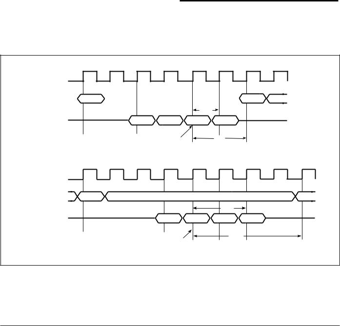
IS42S16128 |
ISSI® |
Read With Auto-Precharge
The read with auto-precharge command first executes a burst read operation and then puts the selected bank in the precharged state automatically. After the precharge completes, the bank goes to the idle state. Thus this command performs a read command and a precharge command in a single operation.
During this operation, the delay period (tPQL) between the last burst data output and the start of the precharge operation differs depending on the CAS latency setting.
When the CAS latency setting is one, the precharge operation starts a the same time as the last burst data is output (tPQL = 0). When the CAS latency setting is two,
the precharge operation starts on one clock cycle before the last burst data is output (tPQL = –1). When the CAS latency setting is three, the precharge operation starts on two clock cycles before the last burst data is output (tPQL = –2). Therefore, the selected bank can be made active after a delay of tRP from the start position of this precharge operation.
The selected bank must be set to the active state before executing this command.
The auto-precharge function is invalid if the burst length is set to full page.
CAS Latency |
3 |
2 |
tPQL |
–2 |
–1 |
CLK
COMMAND READA 0
  ACT 0
ACT 0
|
tPQL |
I/O |
DOUT 0 DOUT 1 DOUT 2 DOUT 3 |
CAS latency = 2, burst length = 4 |
PRECHARGE START |
tRP |
|
READ WITH AUTO-PRECHARGE |
|||
|
|||
(BANK 0) |
|
|
CLK |
|
|
|
|
|
COMMAND |
READA 0 |
|
|
|
ACT 0 |
|
|
|
|
tPQL |
|
I/O |
|
DOUT 0 |
DOUT 1 |
DOUT 2 |
DOUT 3 |
READ WITH AUTO-PRECHARGE |
PRECHARGE START |
|
tRP |
|
|
|
|
|
|||
|
(BANK 0) |
|
|
|
|
CAS latency = 3, burst length = 4
Integrated Silicon Solution, Inc. — 1-800-379-4774 |
23 |
Rev. A
03/13/00
 Loading...