

Page 1

Intel® LXD972M Transceiver
Demo Board (Board Rev A1)
Preliminary User’s Guide
October 2004
Document Number: 303125
Revision Date: October 22, 2004
Revision Number: 002
Page 2

INFORMATION IN THIS DOCUMENT IS PROVIDED IN CONNECTION WITH INTEL® PRODUCTS. NO LICENSE, EXPRESS OR IMPLIED, BY
ESTOPPEL OR OTHERWISE, TO ANY INTELLECTUAL PROPERTY RIGHTS IS GRANTED BY THIS DOCUMENT. EXCEPT AS PROVIDED IN
INTEL'S TERMS AND CONDITIONS OF SALE FOR SUCH PRODUCTS, INTEL ASSUMES NO LIABILITY WHATSOEVER, AND INTEL DISCLAIMS
ANY EXPRESS OR IMPLIED WARRANTY, RELATING TO SALE AND/OR USE OF INTEL PRODUCTS INCLUDING LIABILITY OR WARRANTIES
RELATING TO FITNESS FOR A PARTICULAR PURPOSE, MERCHANTABILITY, OR INFRINGEMENT OF ANY PATENT, COPYRIGHT OR OTHER
INTELLECTUAL PROPERTY RIGHT.
Intel products are not intended for use in medical, life saving, life sustaining, critical control or safety systems, or in nuclear facility applications.
Intel may make changes to specifications and product descriptions at any time, without notice.
Designers must not rely on the absence or characteristics of any features or instructions marked “reserved” or “undefined.” Intel reserves these for
future definition and shall have no responsibility whatsoever for conflicts or incompatibilities arising from future changes to them.
®
The Intel
deviate from published specifications. Current characterized errata are available on request.
Contact your local Intel sales office or your distributor to obtain the latest specifications and before placing your product order.
Copies of documents which have an ordering number and are referenced in this document, or other Intel literature may be obtained by calling
1-800-548-4725 or by visiting Intel's website at http://www.intel.com.
Intel and the Intel logo are trademarks or registered trademarks of Intel Corporation or its subsidiaries in the United States and other countries.
*Other names and brands may be claimed as the property of others.
Copyright © 2004, Intel Corporation.
LXD972M Transceiver Demo Board (Board Rev A1) may contain design defects or errors known as errata which may cause the product to
2 Preliminary User’s Guide
Document Number: 303125
Revision Date: October 22, 2004
Revision Number: 002
Page 3

Contents
Contents
1.0 Introduction......................................................................................................................................5
1.1 About this Demo Board Kit .............................................................. ....... ....... ....... ....... ....... ..5
1.2 Related Documents..............................................................................................................5
1.3 Features of Intel
®
2.0 Using the Intel
LXD972M Demo Board ......................................................................................... 7
2.1 Equip men t Requ irements............................................................................................... ......7
2.2 Typi ca l Test Setup.................................................................................... ............................ 8
2.3 Quick-Start Checklists ..........................................................................................................9
2.4 Configurations..................................................................................................................... 11
2.4.1 Optional Test Setup, Using Two Intel
2.4.2 Power Supply Voltage Source and Clock Options.................................................12
2.4.3 MDIO Configur at ion Options..................................................................................13
2.4.4 LED Configuration Options........... .........................................................................13
2.4.5 CFG Pin Configur at ion Options.............................................................................14
2.5 JTAG Test Signals..............................................................................................................14
3.0 Intel
®
LXD972M Demo Board Schematics....................................................................................15
®
LXD972M Demo Bo ard............................................................................ 6
®
LXD972M Demo Boards ..........................11
4.0 Bill of Ma t e ria ls .............. .. . .. .... . .. .. ... .. .. ............ ............ ... .. .. ............ .... . .. .. . .... .. . .. .... . .. .. ....................20
Figures
1 Typical Test Setup .......................................................................................................................8
2Intel
3 Optional Test Setup ...................................................................................................................11
4 Schematic: Intel
5 Schematic: Intel
6 Schematic: Intel
7 Schematic: Intel
®
LXD972M Transceiver De mo Board ............................... ....................... ........................ ..10
®
LXD972M Transceiver Demo Board Power Control ......................................16
®
LXD972M Transceiver Demo Board MII Port.................................................17
®
LXD972M Transceiver Demo Board Twisted-Pair Port..................................18
®
LXD972M Transceiver Demo Board Configuration.. ...................................... 19
Tables
1 Related Documen ts............................................................................................. .........................5
2 Quick-Start Checklist for Jumper Settings ....................................................................................9
3 Quick-Start Checklist for Switch Settings .....................................................................................9
4 Power Supply Voltage Source Connector Options..................................................................... 12
5 Magnetic Center-Tap Voltage Source Configuratio n Options ... ..................................................12
6 Analog Power Supply (VCCA) Configuration Options ................................................................12
7 Clock Configuration Options.......................................................................................................13
8 MDIO Configurati o n Options............. ............................... ...................................... .....................13
9 Jumper Configuration Settings for LED/CFG Pins...................................................................... 14
10 JTAG Test Signal Descriptions...................................................................................................14
11 Bill of Mate rials ....... ....................................................................................................................20
Preliminary User’s Guide 3
Document Number: 303125
Revision Number: 002
Revision Date: October 22, 2004
Page 4
Contents
Revision History
Page Description
5 Section 1.1, “About this Demo Board Kit”. Text added.
6 Section 1.3, “Features of Intel
7 Section 2.1, “Equipment Requirements”. Text changed.
Section 2.3, “Quick-Start Checklists”. Text changed.
Text changed in Table 2 “Quick-Start Checklist for Jumper Settings”.
9
Text changed in Table 3 “Quick-Start Checklist for Switch Settings”.
Figu re 2 “Intel
12
13
13 Section 2.4.4, “LED Co nfiguration Opt ions”. Text changed.
14 Section 2.4.5, “CFG Pin Configuration Options”. Text change d and new t able added.
15 Section 3.0, “Intel
20 Section 4.0, “Bill of M aterial s”. Text in Table 11 “Bill of Materials” ch anged.
Section 2.4.2 , “Power Supply Voltage Source and Cloc k Options” .
Text changed in Table 4 “Power Supply Voltage Source Connecto r Options” changed.
Section 2.4.3, “MDIO Configuration Options”. Text changed.
Text changed in Table 4 “Power Supply Voltage Source Connecto r Options” changed.
Revision Number 002
Revision Date: October 2004
®
LXD972M Demo Board”. Text changed.
®
LXD972 M Transceiver D emo Board” changed.
®
LXD972M Demo Board Schematics”. Schematics changed.
Revision Number 001
Revisio n Date: July 2004
Page Description
Initial release.
4 Preliminary User’s Guide
Document Number: 303125
Revision Date: October 22, 2004
Revision Number: 002
Page 5
Intel® LXD972M Transceiver Demo Board (Board Rev A1)
1.0 Introduction
This document describes the typical hardware set-up procedures for the Intel® LXD972M
Transce iver Demo Board (called hereafter the LXD972M Demo Board). The LXD972M Demo
Board is a platform for evaluation of the Intel LXT972M Single-Port 10/100 Mbps PHY
Transceiv er (c al le d he re af t er th e LX T 9 72 M Trans c ei ve r ) .
The LXD972M Demo Board allows syste m designers to test the following:
• 10 Mbps and 100 Mbps link perform ance
• Auto-negotiation
• Register func tionality
The LXD972M Demo Board requires only a single 3.3V power supply.
1.1 About this Demo Board Kit
This Demo Board kit includes the following:
• LXD972M Demo Board
®
• Intel
LXD972M Transceiver Demo Board (Board Rev A1) User’s Guide
1.2 Related Documents
Table 1 lists related documen tation.
T able 1. Related Documents
®
Intel
LXT972M S ingle-Port 10/100 Mbps PHY Transceiver Datashee t 30287 5
Intel® LXT971A, LXT972A, LXT972M Single-Port 10/100 Mbps PHY Transceivers
Specification Update
Document Document Number
249354
Preliminary User’s Guide 5
Document Number: 303125
Revision Number: 002
Revision Date: October 22, 2004
Page 6

Intel® LXD972M Transceiver Demo Board (Board Rev A1)
1.3 Features of Intel® LXD972M Demo Board
• 3.3V operation , with option for 2.5V I/O voltage
• Low power consumpti on (300 mW typical)
• Quick setup and clear visibility of application settings for complete system demonstration
• Auto-negotiation protocol compliant. Compatible with system s not supporting auto-
negotiation.
• LED indicators for major functions
• JTAG boundary scan port
• Configurable through MDIO port or hardware jumpers
• Standard half-duplex or full-duplex operation at 10 Mbps or 100 Mbps
6 Preliminary User’s Guide
Document Number: 303125
Revision Date: October 22, 2004
Revision Number: 002
Page 7

Intel® LXD972M Transceiver Demo Board (Board Rev A1)
2.0 Using the Inte l® LXD972M Demo Board
This document i ncl udes infor mati on on the fol lowi ng ite ms conc erni ng usi ng the LXD972M Demo
Board:
• Section 2.1, “Equipment Requirements ” on page 7
• Section 2.2, “Typical T est Setup” on page 8
• Section 2.3, “Quick-Start Checklists” on page 9
• Section 2.4, “Configurations” on page 11
• Section 2.5, “JTAG Test Signals” on page 14
• Chapter 3.0, “Intel
• Chapter 4.0, “Bill of Materials”
2.1 Equipment Requirements
The LXD972M Demo Board is populated with all components needed for twisted-pair evaluation.
However, the following additi onal equipment is also requ ired:
®
LXD972M Demo Boa rd Schematics”
• SmartBits Advanced Multi-port Performance Test Box configured with firmware version 4.39
or newer
• PC with Smart Windows (version 6.0 or newer) insta lled
• One MII C ab l e (male to mal e)
• One external NIC card
• One Category 5 Unshielded Twisted-Pair (UTP) crossover cable
• External power supply
Preliminary User’s Guide 7
Document Number: 303125
Revision Number: 002
Revision Date: October 22, 2004
Page 8
Intel® LXD972M Transceiver Demo Board (Board Rev A1)
2.2 Typical Test Setup
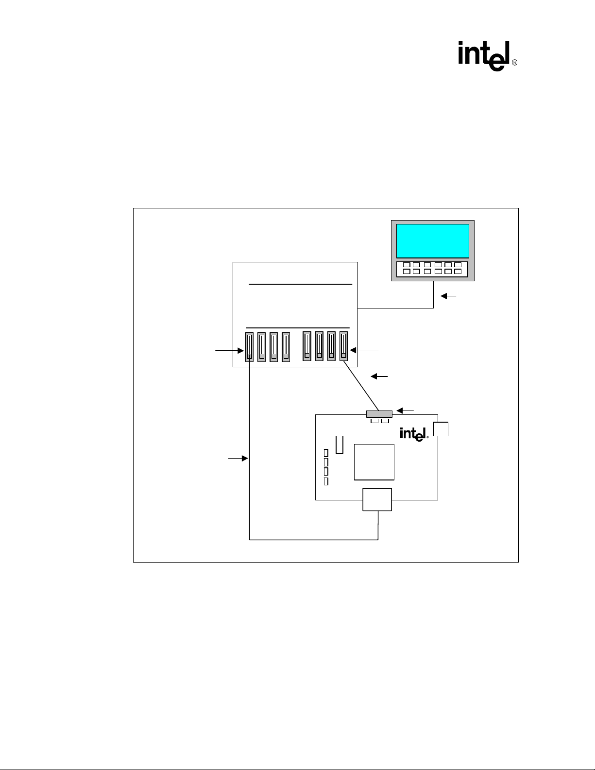
Figure 1 shows a typical tes t setup for standard operation of the LXD972M Demo Board.
The LXD972M Demo Board plugs int o a Smar tBits Advanced Performan ce Test Box through a
standard 40- pin MII cable (not included with the LXD972M Demo Board). The LXD972M Demo
Board RJ-45 jack connects to the RJ-45 card in the SmartBits test box through a Twisted-Pair
cable. Operation can be set for eva luation of 10 Mbps, 100 Mbps, and auto-negotia tion capabilities.
Figure 1. Typical Test Setup
SmartBits
Computer with
Smart Windows
RJ-45 Card
or
External NIC Cards
Twisted Pair
Crossover
Cable
Advanced Multi-port
Performance
Tester
RS-232
MII
Cards
MII Cables
MII
Connectors
LXD972M
LXT972M
B3570-03
8 Preliminary User’s Guide
Document Number: 303125
Revision Date: October 22, 2004
Revision Number: 002
Page 9

Intel® LXD972M Transceiver Demo Board (Board Rev A1)
2.3 Quick-Start Checklists
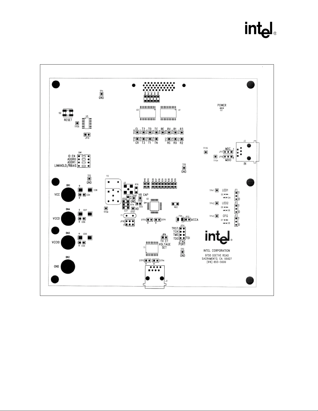
Use the quick-st art checklis t s in this s ecti on to s et up the LXD972M Demo Bo ard, shown in Figure
2, “Intel
®
LXD972M Transceiver Demo Board” on page 10.
The following quick-start setup procedure sets all ports to the default condition, which includes
Auto-Negotiation enabled, advertising dual-speed, and full-duplex/half-duplex capabilities.
1. Set the ju mpers a s li st ed in Table 2.
The following jumpers are defined as follows: LED1 has the func tionality of LED/CFG1,
LED2 has the functio nality of LED/CFG2, and CFG has the func tionality of LED/CFG3 as
defined by the LXT972M Transceiver datasheet.
2. Set SW1 switch es as listed in Table 3.
3. Connect the MII port of the LXD972M Demo Board to the Sm artbits test box through the MII
connector/cable. A male-to-male cable is required to interface the Smartbits test box to the
LXD972M Demo Board and is available from Newark* (.5m cable - Newark 91F9746).
4. Connect the twisted-pair port through a Twisted-Pair crossover cable to the RJ-45 card in the
SmartBits te st box.
5. Power up the Smar tbits test box.
6. When the LXD972M Demo Board is configured according to desired test se ttings, apply the
desired power c onnect ions p er Table 4 options in Sect ion 2. 4.2 , “ Power Supply Voltage So urce
and Clock Options ” on page 12 and press Rese t switch S2.
7. Proc eed with testing.
Table 2. Quick-Start Checklist for Jumper Settings
Jumper Label Setting Configuration
JP1,
JP2,
JP12 VCCA Jumpered
JP16 MDI O Pins 2, 3 Jumper Ro utes MDIO t hrough MII 40-pin Connector P1.
JP17 MDC Pi ns 2, 3 Jumper Routes M DC throug h M II 40-pin Connector P1.
JP18 Clock Select
JP19 Reset Pins 1,2 Jumper Connects reset button
JP3
LED1,
LED2,
CFG
Pins 1, 2 Jumper
Pins 1, 2 Open Disables output of clock oscillator Y2.
Pins 3, 4
Pins 5, 6
Jumper
Jumper
Table 3. Quick-Start Checklist for Switch Settings
Switch / Label Setting Configuration
SW1-1 / ID EN Off Not applicable for LXT972M Transceiver.
SW1-2 / ADDR0 Off Sets ADDR0 = 0 (“Off” position)
SW1-3 / ADDR1 Off Sets ADDR1 = 0 (“Off” position)
SW1-4 / LINKHOLD / RBIAS Off Not applicable for LXT972M Transceiver.
"Sets Port Configuration to 111 for Auto-Negotiation,
10/100 Mbps, Full-Duplex. For details, see Section
2.4.5, “CFG Pin Configuration O ptions” on page14.
Routes power from VCCD connector (BN4) through
JP12 to the VCCA input.
Connects crystal across XI and XO to enable Y1.
Preliminary User’s Guide 9
Document Number: 303125
Revision Number: 002
Revision Date: October 22, 2004
Page 10
Intel® LXD972M Transceiver Demo Board (Board Rev A1)
B3798-001
®
Figure 2. Intel
LXD972M Transceiver Demo Board
SILKSCREEN TOP
BOARD ID
SERIAL #
Note: In Figure 2, the format of the Board ID on the LXD972M Transceiver Demo Board can be either
one of the following:
• For leaded: LXD972M Rev.A1
• For lead-free: LXD972MLF Rev.A1
In Figure 2, the format of the Serial Number on the LXD972M Transceiver Demo Board can be
either one of the following:
• For leaded: 972M-xxxx-A1
• For lead-free: 972MLF-xxxx-A1
10 Preliminary User’s Guide
Document Number: 303125
Revision Date: October 22, 2004
Revision Number: 002
Page 11
Intel® LXD972M Transceiver Demo Board (Board Rev A1)
2.4 Configurations
2.4.1 Optional Test Setup, Using Two Intel® LXD972M Demo Boards
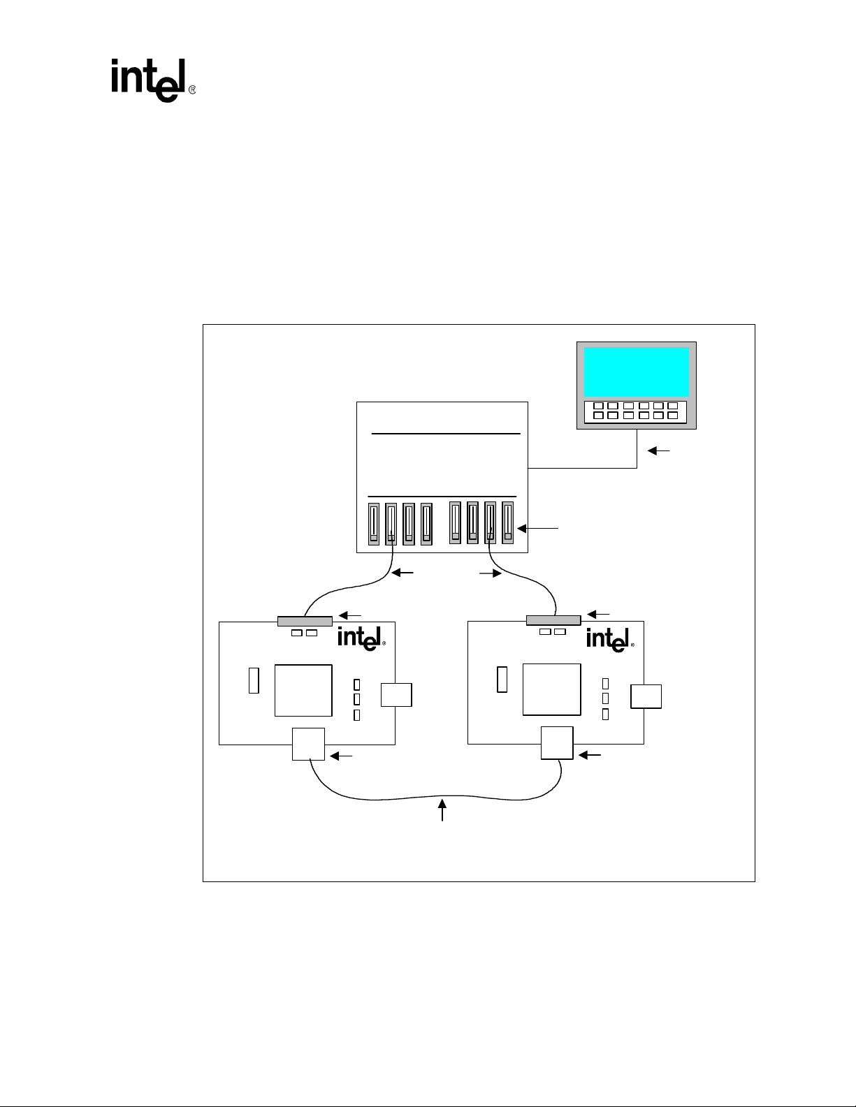
Figure 3 shows an option al test setu p using t wo L XD972M Demo Boards. E ach Demo Bo ard p lugs
into a SmartBit s Adva nce d P erformance Test Box through standard 40-pin MII cables. The two
LXD972M Demo Boards a re linke d th rough a Twisted-Pair crossove r cabl e conne cted t o the RJ -45
jack on each board. Operation can be set for evaluation of 10 Mbps, 100 Mbps, and autonegotiation capabilities.
Figure 3. Optional Test Setup
Computer with
Smart Windows
SmartBits
LXT972M
Connector
LXD972M
RJ-45
Advanced Multi-port
Performance
MII Cable
MII
Twisted-Pair
Crossover
Cable
RS-232
Tester
MII
Cards
MII
Connector
LXD972M
LXT972M
RJ-45
B3572-05
Preliminary User’s Guide 11
Document Number: 303125
Revision Number: 002
Revision Date: October 22, 2004
Page 12

Intel® LXD972M Transceiver Demo Board (Board Rev A1)
2.4.2 Power Supply Voltage Source and Clock Options
Table 4 lists banana lead power connectors (BNn) for the LXD97 2M Demo Board. For details on
the power supplies, see the schematic in Chapter 3.0, “Intel
®
LXD972M Demo Board
Schematics”.
Table 4. Power Supply V oltage Source Connector Options
Reference
Designators
BN1 VCC
BN2 GND Ground
BN3 VCCIO
BN4 VCCD
Signal Supply Description
+3.3V.
For components on the LXD972M D em o Board other than LXT972M Transceiver.
+3.3V or +2.5V.
I/O voltage for the LXT972M Transceiver.
+3.3V.
LXT972M digital pow er. If JP12 jum per is on, analog power is provided for the
LXT972M Transceiver .
Table 5 lists internal and external jumper settings to configure the power supply source for the
transm i t mag n etic ce nter -t ap v ol ta g e.
Table 5. Magnetic Center-Tap Voltage Source Configuration Options
Desired
Power Supply Source
3.3V Power Supply from
VCCA
Alternate Power Supply
Setting Description
Jum per
JP4
Op en
JP4
Use Jumper JP4 to apply 3.3V power fr om VCCA for center-tap
operation.
Use Jumper JP4 to supply either 2.5V or 3.3V power supply for
cente r-tap operation. Connec t the power supply to pin 2 of JP4.
Table 6 lists the LXT972M Demo Board analog power supply (VCCA) configuration options.
Table 6. Analog Power Supply (VCCA) Configuration Options
Analog
Desired
Configuration
3.3V Power
Supply to VCCA
External Power
Supply to VCCA
Setting Description
Jumper
JP12
Open
JP12
Use Jumper JP12 to route power from the VCCD Power Connector
(BN4) t hrough JP 12 to the VCCA input of the LXT972M Transceiver.
1. Remov e jum p er fr om JP1 2 to di sable for V CC A inp ut.
2. Apply ex te r na l power from an alterna t e po w er supply th ro ugh
pin 2 of JP12. For power supply requir ements, see t he LXT972M
Transceiver datas heet.
12 Preliminary User’s Guide
Document Number: 303125
Revision Date: October 22, 2004
Revision Number: 002
Page 13

Intel® LXD972M Transceiver Demo Board (Board Rev A1)
Table 7 lists clock confi guration options.
T able 7. Clock Configuration Options
Desired
Configuration
Enable Cryst al
Oscill ator Y1
Enable Clock
Oscill ator Y2
1. Pin 1 is located on the lower-right corner of JP18.
JP18 Set tings Description
1
, 2 Open
Pins 1
Pins 3, 4
Pins 5, 6
Pins 1, 2 Jumper
Pins 3, 4
Pins 5, 6
Jumper
Open
Remove jumper f rom pins 1 and 2 to disable the clock oscillator Y2
output.
Place a jumper on pins 3 and 4 and pins 5 and 6, which connects a
crystal across XI and XO to enable Y1.
Place a jumper on pins 1 and 2, which enables the output of clock
oscillator Y2.
Remov e jumper from pin s 3 and 4, and remove ju m per from pins 5
and 6, which disables a crystal connection across XI and XO to Y1.
2.4.3 MDIO Configuration Options
The default configuration of the MDIO and MDC signals is to route the MDIO through the MII
connector to the SmartBits Test Box by installing jumpers JP16 and JP17.
Note: The RJ-11 feature is not supported. As a resu lt, do not jumper the MDIO and MDC signals to the
RJ-11 connec to r.
Table 8 lists the desired MDIO configura tion settings.
T able 8. MDIO Configuration Options
Desired Configuration Jumper Setti ng Descr iption
Route MDIO and MD C
through MII
Route MDIO and MD C
through RJ-11
JP16 Jumper P ins 2, 3 Routes MD IO throug h 40-pin MI I Connec tor P1
JP17 Jumper Pins 2, 3 Routes MDC through 40-pin MII Connector P1
JP16 Jumper Pins 1, 2 Routes MDIO through RJ-11 Connector J2
JP17 Jumper Pins 1, 2 Routes MDC through RJ-11 Connector J2
2.4.4 LED Configuration Options
The LXD972M Demo Board provides three programmable LEDs. Each LED can display one of
several avail able status condit ions as selected by the LED Configuration Register (Address 20).
Programmable LEDs (LED/CFG1, LED/CFG2, LED/CFG3) are set in default mode and are
programmable with the MDIO pin. Register address 20 als o provides optional LED puls e
stretching up to 100 ms. Register bits 20.3: 2 select one of three possible st retch times. (For details,
see the LXT972M Tran sc eiver da ta sh eet.)
Note: The active LED state is det erm ined by the CFG pin functio n. When the LED/CFG pin is pulled
High, the LED becomes act ive Low. When the LED/CFG pin is pulled Low, the LED becomes
active High.
Preliminary User’s Guide 13
Document Number: 303125
Revision Number: 002
Revision Date: October 22, 2004
Page 14

Intel® LXD972M Transceiver Demo Board (Board Rev A1)
2.4.5 CFG Pin Configuration Options
Three control jumpers pull the associ ated port configuration pins High or Low to select the des ired
mode (auto-negotiation, speed, and duplex). When auto-negotiation is enabled with LED/CFG1
(JP1) = 1, then LED/CFG2 (JP 2), and LED/CFG3 (JP3) are used to configure default advertising
characteristics of the LXD972M Demo Board. The de si red modes and jumper configuration
settings ar e listed in Table 9. For specific register defi nitions and functions, see the LXT972M
Transceiver datasheet.
Table 9. Jumper Configuration Settings for LED/CFG Pins
Mode Jumper Settings
Auto-
Negotiation
Disabled
Enabled
Speed Duplex
10
100
100
10/100
Half
Full Pins 2 & 3 Pins 2 & 3 Pins 1 & 2
Half Pi ns 2 & 3 Pins 1 & 2 Pins 2 & 3
Full Pins 2 & 3 Pins 1 & 2 Pins 1 & 2
Half Pi ns 1 & 2 Pins 2 & 3 Pins 2 & 3
Full /
Half
Half Pi ns 1 & 2 Pins 1 & 2 Pins 2 & 3
Full /
Half
2.5 JTAG Test Signals
The boundary scan test port is accessed through JP14 for board level testing. Table 10 lists the
JTAG test signal descriptio ns.
Table 10. JTAG T est Signal Descriptions
JP14 Pin
Number
Symbol Description
LED/CFG1
Jumper
JP1
Setting
Pins 2 & 3
Jumper
Pins 1 & 2 Pins 2 & 3 Pins 1 & 2
Pins 1 & 2 Pins 1 & 2 Pins 1 & 2
JP2
LED/CFG2
Setting
Pins 2 & 3
Jumper
JP3
LED/CFG3
Setting
Pins 2 & 3
1TRST_LTest Reset. Test reset input sou rced by te sting device.
3TCK
5TMS
7TDO
8TDI
T est Clock. Test clock input sourced by testing device.
Test Mode Select.
Test Data Output. Test data driven with respect to the falling edge of TCK.
Test Data Input. Test data sampled with respect to the rising edge of TCK.
14 Preliminary User’s Guide
Document Number: 303125
Revision Date: October 22, 2004
Revision Number: 002
Page 15

Intel® LXD972M Transceiver Demo Board (Board Rev A1)
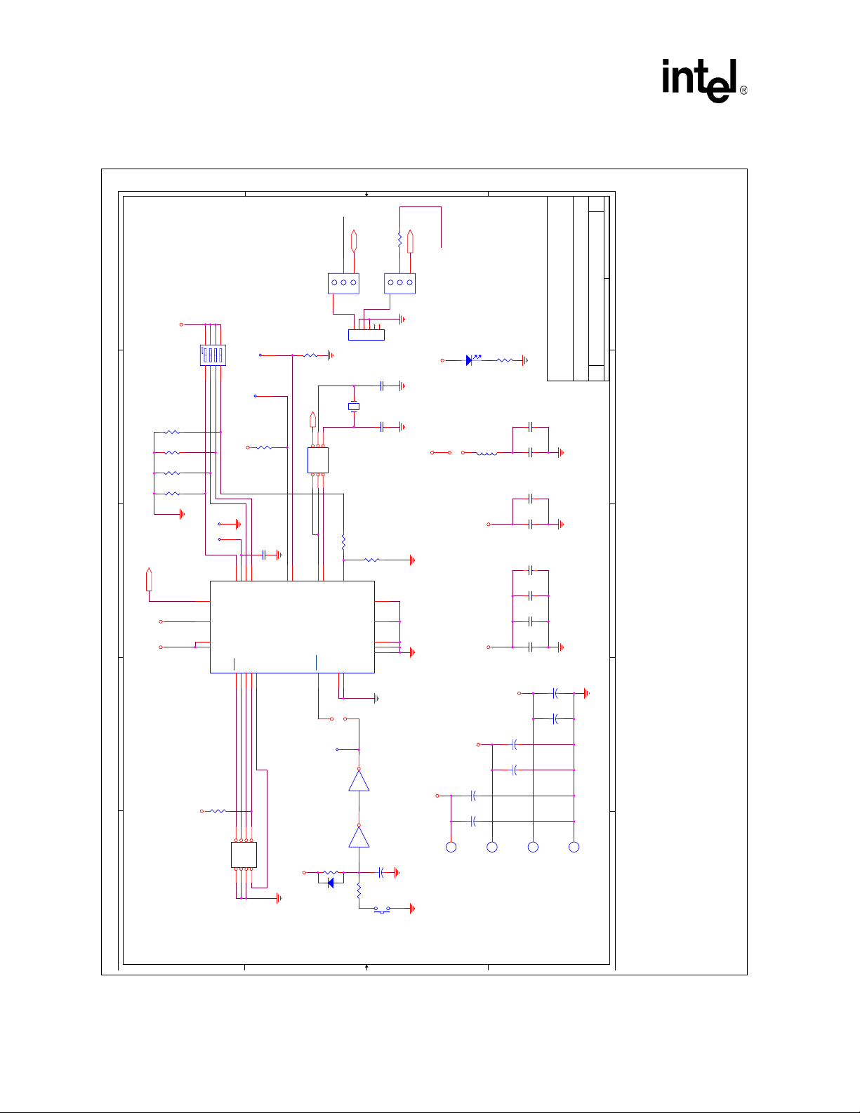
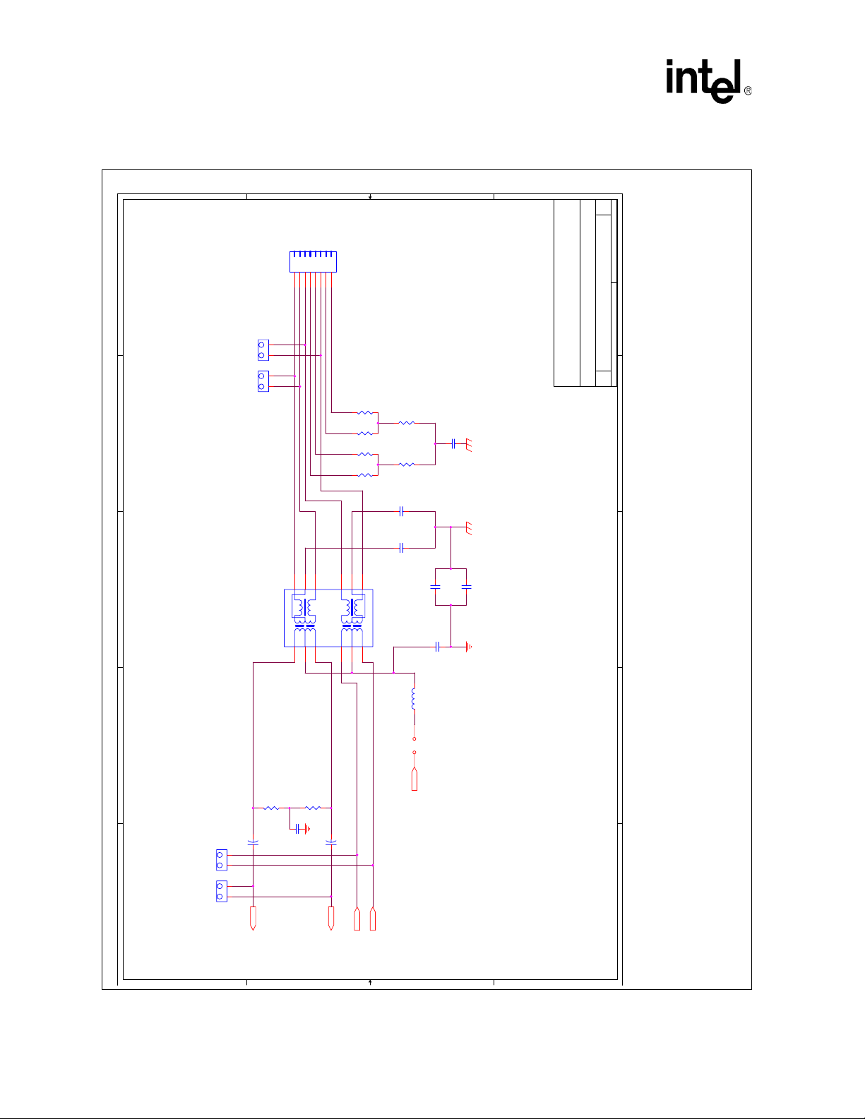
3.0 Intel® LXD972M Demo Board Schematics
This section includes schematics for the LXD972M Demo Board:
• Figure 4, “Sch em atic: Int el
• Figure 5, “Sch em atic: Int el
• Figure 6, “Sch em atic: Int el
page 18
• Figure 7, “Sch em atic: Int el
Note: Page 1 of 5 of the schematics is no t included (the title page of th e schematics ).
®
LXD972M Transceiver Demo Board Power Control” on page 16
®
LXD972M Transceiver Demo Board MII Port” on page 17
®
LXD972M Transceiver Demo Board Twisted-Pair Port” on
®
LXD972M Transceiver Demo Board Configuration” on page 19
Preliminary User’s Guide 15
Document Number: 303125
Revision Number: 002
Revision Date: October 22, 2004
Page 16
Intel® LXD972M Transceiver Demo Board (Board Rev A1)
Figure 4. Schemati c: Intel® LXD972M Transceiver Demo Board Power Control
MDIO_1
MDIO
E
2
3
1
JP16
HEADER 3_1
MDC_1
MDC
R83 50 1%
2
3
1
JP17
HEADER 3_1
A1
of
25Monday, September 20, 2004
E
VCC
876
5
SW1
123
4
ADDR0
ADDR1
D
C
B
A
VCCA
VCCIO VCCD
R62
4.7k
R61
4.7k
R60
4.7k
R58
4.7k
GND
TP40
TP39
VCCA
16
VCCD
39
29
6
U2A
R65
100K
VCCIO
JTAG PORT
1
1
VCCIO
VCCIO
JP14
SW DIP-4
TP34
VCCIO
GND
7811
10
NC
NC
ADDR0
TCK
TMS
TRST
2322212019
TRST
TCK
TMS
123456
TDO
TP35
ADDR1
TDO
TDI
78
1
1
R66
4.7k
C53X
TDI
HEADER 4X2
MDC
MDIO
GND
32
31
MDC
MDIO
LXT972M_LQFP48C
VCC
GND
R82
X
XIN
JP18
12
34
3
RESET REFCLK/XI
4 2
J2
GND
Y1
HEADER 3X2
56
R73
12
XO
RBIAS
CE/TEST0
GNDIO/TEST1
24
25
JP19
2-pin
1
TP36
U5B
U5A
R67
10K
D1
1N914
12345
25MHz
LXT972M: R73
AND C53 ARE
X
RESET
3 4
1 2
R68
GND
6
RJ11
IN
C33
18pF 25V
GNDGND
C32
18pF 25V
NOT POPULATED
R69
22.1K 1%
GNDA
13
GNDD
38
GNDIO
30
GNDIO
9
GNDIO
5
GND
74LVX14
74LVX14
C31
10uF
+
GND
100
S2
RESET
VCC
VCCD
GND
GND
VCC
VCC
GND
LED
D2
POWER
FERRITE
FB4
JP12
2-pin
VCCD
VCCIO
VCCIO
C36
100uF
+
C34
10uF
+
1
BN3
BN1
VCCIO
LXT972M: 3.3V
R72
220
1
GND
C7
.001uF
C6
0.1uF
VCCA
C52
.001uF
C51
0.1uF
C12
.001uF
C10
0.1uF
C4
.001uF
C3
0.1uF
VCCD
C55
100uF
+
C54
10uF
+
1
BN4
VCCD
LXT972M: 3.3V
Intel Corporation
9750 Goethe Road
Sacramento, CA 95827
GND
GND GND
C57
100uF
+
C56
10uF
+
1
BN2
Intel(R) LXD972M Transceiver Demo Board CONTROL/POWER
LXD972M LQFP48C DV/DEMO
B
Title
Size Document Number Rev
Date: Sheet
D
X=DO NOT INSTALL
C
GND
B
GND
A
4 4
3 3
2 2
1 1
16 Preliminary User’s Guide
Document Number: 303125
LXT972M: 2.5V/3.3V
Revision Date: October 22, 2004
Revision Number: 002
Page 17

Intel® LXD972M Transceiver Demo Board (Board Rev A1)
Figure 5. Schematic: Intel® LXD972M Transceiver Demo Board MII Port
TPFOP
TPFON
TPFIP
TPFIN
LED/CFG2
LED/CFG3
E
TP43
TP42
TP41
LED/CFG1
1
1
1
LED/CFG2
LED/CFG3
282726
LED/CFG1
151418
17
TPFIP
TPFIN
TPFOP0
TPFON0
Intel Corporation
9750 Goethe Road
Sacramento, CA 95827
A1
of
35Monday, September 20, 2004
E
Intel(R) LXD972M Transceiver Demo Board MII PORT
LXD972M LQFP48C DV/DEMO
B
Title
Size Document Number Rev
Date: Sheet
R41
TXD0
T1T0T3
50 1%
R42
TXD1
T2
50 1%
R43
TXD2
50 1%
R44
TXD3
COL
CRS
1
48
R45 22
LXT972M_LQFP48C
X
R81
X
R80
X
R79
X
R78
X
R77
R48 22
1
TP30
1
TP29
TP28
1
1
TP27
1
TP26
1
TP25
1
TP24
2468111315171
1A1
1A2
1A3
1A4
2A2
2A3
2A4
SN74LVC244A
VCCGND
2010
VCC
1Y1
1Y2
1Y3
1Y4
2Y2
2Y3
2Y4
U3
3
181614
12
R47 50 1%
R46 50 1%
20
D
GND
C
VCC
GND
19
1G
2G
2A1
GND
2Y1
975
C15
0.1uF
VCC
GND
X=DO NOT INSTALL
B
U2B
RXD3
RXD2
RXD1
RXD0
RX_DV
RX_CLK
RX_ER
TX_CLK
D
1
TP22
1
TP21
1
TP20
1
TP19
1
TP18
1
TP17
1
TP16
1
C
B
TP15
SN74LVC244A
2010
VCC
U1
C14
0.1uF
VCC
GND
33343536374041424344454647
22
R26
22
R28
22
R30
22
R32
R34
R36
R0TCR1R2RV
R3
RC
RE
2468111315171
1A1
1A2
1A3
1A4
2A1
2A2
2A3
2A4
VCCGND
1Y1
1Y2
1Y3
1Y4
2Y1
2Y2
2Y3
2Y4
975
3
181614
12
50 1%
R27 50 1%
R31 50 1%
R25 50 1%
R24 50 1%
R29 50 1%
R35
R33 50 1%
R23 50 1%
12345678910111213141516171819
TX_EN
22
22
22
R37
22
R38
GND
19
TNCRCL
1G
2G
GND
50 1%
50 1%
R40
P1
21222324252627282930313233343536373839
A
MDC_1
MDIO_1
4 4
3 3
MII 40 PIN
40
GND
2 2
1 1
A
Preliminary User’s Guide 17
Document Number: 303125
Revision Number: 002
Revision Date: October 22, 2004
Page 18
Intel® LXD972M Transceiver Demo Board (Board Rev A1)
Figure 6. Schemati c: Intel® LXD972M Transceiver Demo Board Twisted-Pair Port
J1
DIFF TP
DIFF TP
1234567
IPINOP
DTP4
+
|
+
|
DTP3
E
D
RJ45
8
ON
LXD972M LQFP48C DV/DEMO
Intel Corporation
9750 Goethe Road
Sacramento, CA 95827
Title
Size Document Number Rev
R9
50 1%
R13
50 1%
50 1%
50 1%
50 1%
R12
50 1%
C18
0.001uF 2KV
R8
R7
R6
A1
of
45Monday, September 20, 2004
E
Intel(R) LXD972M Transceiver Demo Board TP PORT
B
Date: Sheet
D
C48
0.001uF 2KV
C47
0.001uF 2KV
6
7
8
Halo TG110-S050N5
9
11
141516
10
FB5
FERRITE
JP4
50 1%
C44
270pF
JUMPER 1X1
VCCA
C59
C58
TX CT VOLTAGE SET
0.001uF 2KV
C49
0.01uF
0.001uF 2KV
GND
C
B
A
TP PORT
T1
R4
50 1%
270pF
213
R5
GND
C17
0.01uF
C
B
DTP2
C43
+
|
DIFF TP
+
A
DIFF TP
|
DTP1
TPFIP
4 4
TPFIN
TPFON
TPFOP
3 3
2 2
1 1
18 Preliminary User’s Guide
Document Number: 303125
Revision Date: October 22, 2004
Revision Number: 002
Page 19

Intel® LXD972M Transceiver Demo Board (Board Rev A1)
Figure 7. Schematic: Intel® LXD972M Transceiver Demo Board Configuration
of
55Monday, September 20, 2004
E
E
VCCIO
1
TP5
TP4
TP3
D
TP2
DISTRIBUTE, LABEL AS "GND"
C
B
GND
1
1
1
D3
LED1
JP1
123
LED
R1
TP38
LED
LED/CFG1
1
VCC
HEADER 3 PIN
D4
180
GND
FB6
FB3
LED2
X
FERRITE
VCCIO
VCCIO
GND
123
JP2
D5
LED
LED
R2
LED/CFG2
Y2
C16
0.1uF
0.1uF
C50
HEADER 3 PIN
D6
180
1
NC
VCC
14
VCCX
JP3
D7
CFG
78
GNDOUT
R70
50 1%
GND
123
HEADER 3 PIN
D8
LED
LED
R3
180
LED/CFG3
GND
25MHzCRYSTAL OSC
234
5
J3 SMB
1
X
R76
R75
GND
50 1%
Intel(R) LXD972M Transceiver CAPS, LED CONFIG., MISC. A1
LXD972M LQFP48C DV/DEMO
Intel Corporation
9750 Goethe Road
Sacramento, CA 95827
B
Title
Size Document Number Rev
Date: Sheet
D
C
GND
X=DO NOT INSTALL
B
GND
1
TP37
R74
0
C37
20pF
GND
A
4 4
3 3
XIN
2 2
1 1
A
Preliminary User’s Guide 19
Document Number: 303125
Revision Number: 002
Revision Date: October 22, 2004
Page 20

Intel® LXD972M Transceiver Demo Board (Board Rev A1)
4.0 Bill of M a te r ials
Table 11 lists the bill of materials for the LXD972M Demo Board Rev A1.
Table 11. Bill of Materials (Sheet 1 of 3)
Board Reference
Designator
BN1-4
C1, C2, C5, C8, C9, C11,
C13, C38-C42, C45, C46
C3, C6, C10, C14-16,
C50-51
C4, C7, C12, C52
C17, C49
C53 (NOT INSTALLED) NOT INSTALLED X 1
C18, C47-48, C58-59
C31, C34, C54, C56
C32-33 CAP 18 pF 50V 5% (0805) PANASONIC ECU-V1H180JCN 2
C36, C55, C57 CAP 100uF 6.3V (CASED) PANASONIC ECE-V0JA101P 3
C37 CAP 20PF 50V 5% (1206) PANASONIC ECU-V1H200JCM 1
C43-44 CAP 27 0pF NPO (1206) AVX 12061A271JATTA 2
D1
D2-D8
DTP1-4, JP4, JP12, JP19 HEADER 2X1 (SIP\2P) BERG 68000- 240-2 7
FB1, FB2 LABELS NOT USED IN SCHEMATIC.
Descrip t ion Manufacturer Part Number Quanti t y
CONN BANANA NUT
SILVER (BANANA_NUT)
LABELS NOT USED IN SCHEMATIC.
HEADER 3X1 (SIP\3P) BERG 08055C104KATMA 8
HEADER 4X2
(HEADER2X4)
CAP 0.01uF X7R 10%
(0805)
CAP 1000pF 20% 2KV X7R
(1812)
CAP 10 uF 6.3V TANT
(CASEA)
DIODE RECTIFIER DL4001
1A 50V MELF SMD
DIODE LED GREEN SS
TYPE LOW CUR SMD
(LED\SMD\SS)
EF JOHNSON 108-0740-001 4
BERG ECU-V1H102JCX 4
AVX 08055C103KATMA 2
AVX 1812GC102KAT1A 5
PANASONIC ECS-TOJY106R 4
DIODES INC. DL4001-13 1
PANASONIC LNJ308G8LRA 7
FB3-5
FB6 (NOT INSTALLED) NOT INSTALLED X 1
J1
J2
J3
FBEAD 60 OHM@100MHZ
0.10OHM@DC 1. 5A (1210 )
(BEAD3225)
CONN MOD JACK 8-8
LOW PROFILE
CONN MOD JACK 6-6
RJ11 UNSHIELDED
BLOCK RJ11-6L-B
CONN SMB VERTICAL PC
MOUNT (SMB\SM)
STEWARD MI1210K600R-00 3
AMP 555164-1 1
CORCOM RJ11-6L-B 1
JOHNSON
COMPONENTS
131-3711-201 1
20 Preliminary User’s Guide
Document Number: 303125
Revision Date: October 22, 2004
Revision Number: 002
Page 21

Intel® LXD972M Transceiver Demo Board (Board Rev A1)
Table 11. Bill of Materials (Sheet 2 of 3)
Board Reference
Designator
JP5-JP11, JP13, JP15 LABELS NOT USED IN SCHEMATIC.
JP1-3, JP16-17 HEADER 3X1 (SIP\3P) BERG 68000-240-3 5
JP14
JP18 HEADER 3X2 BERG C9192-280-3 1
P1
R1-3
R4-9, R12-13, R23-25,
R27, R29, R31, R33, R35,
R40-44, R46-47, R70,
R76, R82, R83
R26, R28, R30, R32, R34,
R36-38, R45, R48
R58, R6 0- 6 2, R 66 RES 4.7K 1/8W 5% (1 20 6) PANASON I C ER J -8G EYJ472 V 5
R65
R67
R68
R69 RES 22.1K 1/8 W 1% (1206) P ANASONIC ERJ-8ENF2212V 1
R72
R73, R75, R77-R82 (NOT
INSTALLED)
R10, R11, R14-22, R39,
R49-57, R59, R63-64, R71
R74
S2
Description Manufacturer Part Number Quantity
HEADER 4X2
(HEADER2X4)
CONN MII 40 PIN FEMALE
R/A (CON40F\RT\4ROW)
RES 182 OH M 1/8 W 1%
(1206) SMD
RES 49.9 1/8W 1% (1206) PANASONIC ERJ-8ENF49R9V 27
RES 22 OH M 1/8W 1%
(0805)
RES 100K 1/8W 1% (1206)
SMD
RES 10K 1/8W 1% (1 206)
NOTE: R3 is shown as 180
Ohm resist or in
schematic.
RES 100 OH M 1/8 W 1%
(1206)
RES 220 OH M 1/8 W 5%
(1206)
NOT INSTALLED X 8
LABELS NOT USED IN SCHEMATIC.
RES 0 OHM 1/8W 5%
(1206) SMD
SWITCH PB MOM KEY JLEAD SMD
(SWITCH\RESET\SM)
BERG C9192-280-4 1
AMP 787171-4 1
PANASONIC ERJ-8ENF1820V 3
YAGE O AM ERICA
PANASONIC ERJ-8ENF1003V 1
PANASONIC ERJ-8ENF1002V 1
PANASONIC ERJ-8ENF1000V 1
PANASONIC ERJ-8GEYJ221V 1
PANASONIC ERJ-8GEY0R00V 1
C&K
COMPONENTS
9C08052A22R0FK
HFT
KT11P2JM 1
10
SW1
T1
TP2-5, TP15-22, TP24-30,
TP34-43
SWITCH DIP 4 POS THRU
HOLE SEALED BLACK
(SWITCH\8)
IC XFMR TG110-S050N2
16 PIN SOIC
HEADER 1X1 BERG 68000-240-1 29
AMP 4-435166-9 1
HALO TG110-S050N2 1
Preliminary User’s Guide 21
Document Number: 303125
Revision Number: 002
Revision Date: October 22, 2004
Page 22

Intel® LXD972M Transceiver Demo Board (Board Rev A1)
Table 11. Bill of Materials (Sheet 3 of 3)
Board Reference
Designator
TP1, TP6 - 14 , TP 23 ,
TP31-33
U1, U3
U2
U4 LABELS NOT USED IN SCHEMATIC.
U5
Y1
Y2
Descrip t ion Manufacturer Part Nu m ber Quant i t y
LABELS NOT USED IN SCHEMATIC.
IC LOGI C 74LVC244 LOW
VOLTAGE BUFFER 20 PIN
SOIC
IC PHY LXT977/LXT972M
DUAL PORT (LQFP48C)
IC LOGI C 74LVX14 HEX
SCHMITT TRIG INV 14 PIN
SOIC
CRYSTAL 25.000MHZ
(HC49)
OSC 25.000MHZ FULL
SIZE ( )
TEXAS
INSTRUMENTS
INTEL LXT977/LXT972M 1
TOSHIBA TC74LVX14FN 1
CTS MP250 1
CTS MX045-25.0000 1
SN74LVC244ADW 2
22 Preliminary User’s Guide
Document Number: 303125
Revision Date: October 22, 2004
Revision Number: 002
 Loading...