

Page 1

LXD970A Demo Board for 10/100
and 100BASE-FX Applications
Development Kit Manual
January 2001
As of January 15, 2001, this document replaces the Level One document Order Number: 249103-001
LXD970A Demo Board for 10/100 and 100BASE-FX Applications.
Page 2

Information in this document is provided in connection with Intel® products. No license, express or implied, by estoppel or otherwise, to any intellectual
property rights is granted by this document. Except as provided in Intel’s Terms and Conditions of Sale for such products, Intel assumes no liability
whatsoever, and Intel disclaims any express or implied warranty, relating to sale and/or use of Intel products including liability or warranties relating to
fitness for a particular purpose, merchantability, or infringement of any patent, copyright or other intellectual property right. Intel products are not
intended for use in medical, life sav ing, or life sustaining applications.
Intel may make changes to specifications and product descriptions at any time, without notice.
Designers must not rely on the absence or characteristics of any features or instructions marked “reserved” or “undefined.” Intel reserves these for
future definition and shall have no responsibility whatsoever for conflicts or incompatibilities arising from future changes to them.
The LXD970A may contain design defects or errors known as errata which may cause the product to deviate from published specifications. Current
characterized errata are available on request.
Contact your local Intel sales office or your distributor to obtain the latest specifications and before placing your product order.
Copies of documents which have an ordering number and are referenced in this document, or other Intel literature may be obtained by calling
1-800-548-4725 or by visiting Intel's website at http://www.intel.com.
Copyright © Intel Corporation, 2001
*Third-party brands and names are the property of their respective owners.
LXD970A Demo Board for 10/100 and 100B ASE-FX Applications Development Kit Manual
Page 3

Contents
1.0 General Description..................................................................................................5
1.1 Features................................................................................................................5
2.0 Equipment and Setup...............................................................................................7
2.1 Test Setup.............................................................................................................7
2.2 Loading Test File...................... ....... ...... ...... ....... ...... ....... ...... ....... ...... ....... ............7
2.3 Power Supply Option.............................................................................................8
2.3.1 External +5V Supply for Analog Circuitry (VCCA, VCCT and VCCR)..9
2.4 Test Points ............................................................................................................9
3.0 Jumpers.......................................................................................................................10
4.0 Hardware Control Interface..................................................................................11
4.1 Multi-Function Pins..............................................................................................11
4.1.1 Function/Address Settings .................................................................11
4.1.2 Additional Jumper Functions..............................................................12
4.2 LED Indicators.....................................................................................................13
Figures
Tables
1 LXD970A Demo Board..........................................................................................6
2 Basic Test Setup ...................................................................................................7
3 Optional Test Setup..............................................................................................8
4 Hardware Control Interface Jumper Placement .................................................11
5 LXD970A Schematic ...........................................................................................14
1 Test Point Descriptions .........................................................................................9
2 Jumper Descriptions............................................................................................10
3 MF Pins Input Voltage Levels..............................................................................11
4 Hardware Control Interface (JP1) Functions.......................................................12
5 Operating Speed Advertisement Settings ...........................................................12
6 Additional JP1 Jumper Functions........................................................................13
7 LED Descriptions.................................................................................................13
LXD970A Demo Board for 10/100 and 100BASE-FX Applications Development Kit Manual iii
Page 4

Page 5

Demo Board for 10/100 and 100BASE-FX Applications — LXD970A
1.0 General Description
The LXD970A Demo Board is a versatile 10/100Mbps Ethernet media access unit (MAU) that
demonstrates all of the integral features of the LXT970A Fast Ethernet Transceiver.
The LXD970A provides a working platform for evaluation of the LXT970A Fast Ethernet
Transceiver in 10BASE-T and/or 100BASE-TX/FX applications.
The LXD970A Demo Board is configured with a sin gle chip 10/100Mbps , IEEE 802.3u comp liant,
Fast Ethernet Transceiver unit (LXD970 A). Th e demo board is designed to plug into a transceiver
test box via a standard 40-pin MII connector. This allows system designers to test 10Mbps and
100Mbps link performance, auto-negotiation and register functionality prior to board prototyping.
The LXT970A also provides an ECL-type interface for 100BASE-FX link testing.
This document describes typical Demo Board setup procedures for a 100BASE-TX environment.
Before using the Demo Board, review the LXT970A Fast Ethernet Transceiver data sheet for
device functionality and specifications.
1.1 Features
• IEEE 802.3-compliant 10BASE-T and 100BASE-TX using a single RJ45 connection.
• Quick setup, ease of use, and clear visibility of application settings for:
— Complete system demonstration
— Individual circuit isolation
• LED indicators for major functions.
• IEEE 802.3u MII interface with extended register capability.
• Configured for single 5V supply operation.
• Standard half duplex or full duplex operation at 10 or 100 Mbps.
• 100BASE-FX fiber optic capability (unstuffed optional circuitry).
Development Kit Manual 5
Page 6
LXD970A — Demo Board for 10/100 and 100BASE-FX Applications
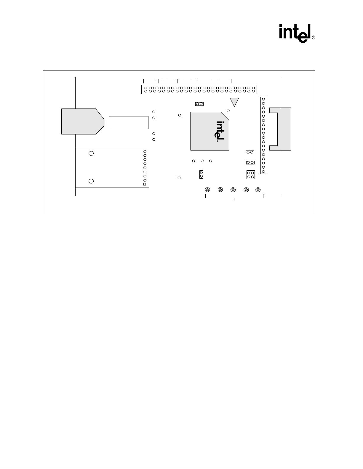
Figure 1. LXD970A Demo Board
RJ-45
FIBER MODULE CIRCUIT
TRANSFORMER
Optional
JP1
TD+
TD -
RD+
RD -
MF1 MF2 MF3 MF4MF0
TEST
JP5
GNDT
A
M
MDINT
0
1
N
2
N
N
A
A
M
M
JP7
LXT970A
MII
JP4
GNDR
TSTON
TSTOPIBTST
JP6
ENBL COL LNK TX RX
JP3
JP8
LEDs
6 Development Kit Manual
Page 7

Demo Board for 10/100 and 100BASE-FX Applications — LXD970A
2.0 Equipment and Setup
The LXD970A Demo Board includes all the components needed for a successful evaluation.
However, the following additional equipment is recommended:
• NetCom System X-1000 transceiver test box configured with firmware version 1.17 or newer.
• PC with Fast Ether Windows (version 1.5 or newer) installed.
• Various lengths of Category 5 Unshielded Twisted-Pair (UTP) cable (1, 20, 40, 60, 80, 100,
120 and 140 meters).
• For 100BASE-FX evaluation, a fiber-optic transceiver module (HFBR-5103) and fiber-optic
cable are required.
2.1 Test Setup
Figure 1 shows a typical test setup for the basic operation of the LXD970A. The LXD970A plugs
directly into a X1000 NetCom Transceiver Test Box via a standard 40-pin MII connector that is
included on the board.
An optional test setup is shown in Figure 2 using a PC for testing additional nodes.
Note: JP3 and JP4 must be installed on the LXD970A for the Netcom System X-1000 transceiver
test box to access the MII management registers inside the LXT970A.
Figure 2. Basic Test Setup
NETCOM
X1000
MII
LXD970A
UTP
Loop
LXD970A
FAST ETHER
Windows
RS232
PC
Development Kit Manual 7
Page 8

LXD970A — Demo Board for 10/100 and 100BASE-FX Applications
2.2 Loading Test File
A disk that contains the file needed for testing is included with the LXD970A demo board.
This file contains “Killer Packets” (100Tx4.s), that exhibit worst case baseline wander
characteristics suitable for evaluating link performance and comparing the LXT970A to alternative
products. Some devices do not adjust well over a range of cable distances. It is recommended to
compare LXT970A performance to similar devices over a wide range of cable lengths.
Follow this simple procedure for loading test file into the Netcom X-1000 test box:
• Load disk containing test pattern into computer
• Start Fast Ether Windows
• Click the “DATA PATTERN” button in the lower left of the screen
• From the Data Pattern options presented, select “CUSTOM”
• From the File menu, select “OPEN”, then select the drive and directory where the test file is
located. (If you are using the disk from Intel, select A:\100Tx4.s)
• When the test file is displayed on screen, select “CLOSE”. This automatically downloads the
test pattern to the Netcom X1000 test box
• Proceed with normal testing
Figure 3. Optional Test Setup
FAST ETHER
NETCOM
FAST ETHER
Windows
Windows
PC
RS232
X1000
MII
Serial
LXD970A
LXD970A
Terminal SW
Termina l SW
PC
HUB
RJ-45
RS232
Port
1
Port 2
UTP
UTP
8 Development Kit Manual
Page 9
Demo Board for 10/100 and 100BASE-FX Applications — LXD970A
2.3 Power Supply Option
The LXD970A includes a jumper (JP8), which provides a an optional power supply source for the
VCC pins; VCCA (analog supply), VCCR (receive supply), VCCT (transmit supply) and VCCD
(digital supply). In the original factory configuration, this jumper is shorted by a circuit trace and
all LXD970A power is supplied via the MII pin (J1). However, the circuit trace can be easily cut to
provide the JP8 isolation option.
2.3.1 External +5V Supply for Analog Circuitry (VCCA, VCCT and VCCR)
To provide an external +5V power supply for the LXD970A analog circuitry, proceed as follows:
• Cut the circuit trace across JP8 pins 3 and 4
• Attach an external +5V supply to JP8 pin 3
This routes the external supply to VCCA, VCCT, and VCCR (all circuits except VCCD and
VCCIO). To restore to factory configuration, disconnect the external power supply and install the
jumper block in JP8.
2.4 Test Points
There are 9 Test Points on the LXD970A Demo Board. Table 1 describes these.
T able 1. Test Point Descriptions
Label Ref Des Description
TD+ J3 Transmit Data Output Positive - Signals transmitted from LXD970A to TP link.
TD- J4 Transmit Data Output Negative - Signal transmitted from LXD970A to TP link.
RD+ J5 Receive Data Input Positive - Signals received from TP network.
RD- J6 Receive Data Input Negative - Signals received from TP network.
GNDA J8 Analog Ground
TSTON J9 Test Output Negative
TSTOP J10 Test Output Positive
IBTST J11 IB Test 1
MDINT J12 Management Data Interrupt
1. Factory Test Only
Ω pull-up to VCC needed if used
2. 4.7k
1
1
2
- Indicates status change.
Development Kit Manual 9
Page 10

LXD970A — Demo Board for 10/100 and 100BASE-FX Applications
3.0 Jumpers
There are 7 Jumpers on the LXD970 Demo Board. Table 2 describes these jumpers and their
functions.
T a ble 2. Jumper Descriptions
Ref Des Function
JP1
JP3
JP4
JP5
JP6
JP7
JP8
Hardware Control Interface: Provides access to voltage sensitive manual control functions. See Tables 3, 4
and 5 for details.
MDIO: Connects the MDIO pin to the MII connector. With the trace cut and the jumper open, the MDIO pin
can be connected to an external device.
MDC: Connects the MDC pin to the MII connector. With the trace cut and the jumper open, the MDC pin can
be connected to an external device.
TEST: This jumper should not be installed for normal operation. This jumper is used to put the chip into a
test mode that is used to characterize the chip.
POWER DOWN: With the jumper installed the chip goes into a power down mode.
In power down mode the MII port (except MDIO and MDC), the twisted pair port and the LED pins are
tristated.
MII: 18-pin straight header that is connected to all the MII interface signal pins. There is a ground test point
next to C20 to ground probes to.
ANALOG VCC CONNECT: Connects MII connector power to the analog portion of the chip.
To use +5V power from MII connector:
No action required. The jumpers (pins 1 & 2 and 3 & 4) are shorted via a trace on the bottom of board.
However, if the traces are cut, the jumpers must be installed to supply power from MII to analog VCC (VCCA).
To use alternate power supply for Analog VCC:
Cut the trace on the bottom of board across pins 3 and 4 shorting JP8. With no jumpers installed, an external
power can be connected. Provide an alternate power supply ( +5V) to pin 3 of JP8.
10 Development Kit Manual
Page 11

Demo Board for 10/100 and 100BASE-FX Applications — LXD970A
4.0 Hardware Control Interface
4.1 Multi-Function Pins
The Hardware Control Interface (JP1) provides access to the Multi-Function (MF) pins which
decode 4-level supply voltages to establish two independent settings per pin. The first setting
determines chip address. The second setting determines configuration of the LXD970A. The 4level inputs referred to as V
Table 3. MF Pins Input Voltage Levels
Parameter Symbol Min Max Units
Input Voltage Level 1 V
Input Voltage Level 2 V
Input Voltage Level 3 V
Input Voltage Level 4 V
MF1, VMF2, VMF3 and VMF4 are shown in Table 3.
MF1 Vcc - 0.5 - V
MF2 (Vcc/2) + 0.5 Vcc - 1.2 V
MF31.2Vcc/2 - 0.5V
MF4- 0.5V
To select an Input Level place a jumper on the appropriate pins. The 4-level input pins (V
VMF2, VMF3 and VMF4) are identical for each Multi-Function (MF) section. See Figure 3 for
jumper placement.
Figure 4. Hardware Control Interface Jumper Placement
MF0
pin 2
pin 1
1
2
MF
MF
V
V
NOTES:
1. TRSTE and MDDIS functions are not labeled on the board.
2. CFG1, CFG0 and FDE are pin names for the manual pins and are not labeled on the board.
MF1 MF2 MF3 MF4
3
4
MF
MF
V
V
MF1,
2
2
)
2
)
0
)
1
E
G
G
F
D
F
1
F
C
(
1
0
N
N
A
A
M
M
1
C
(
(
E
S
2
I
T
N
D
S
A
D
R
M
T
M
pin 50
pin 49
Development Kit Manual 11
Page 12

LXD970A — Demo Board for 10/100 and 100BASE-FX Applications
4.1.1 Function/Address Settings
The multi-function pins allow the user to enable or disable the applicable functions and determine
chip address according to the input level selected. Table 4 shows the status of the function
according to the (V
Table 4. Hardware Control Interface (JP1) Functions
Address Input Voltage Levels
Pin Function VMF1VMF2VMF3VMF4
Address Bit 0 1 1 0 0
MF0
MF1
MF2
MF3
Auto-Negotiation
Sets the initial value of bit 0.12
Address Bit 1 1 1 0 0
Repeater / DTE Mode
Sets the initial value of bit 19.13
Address Bit 2 1 1 0 0
Nibble (4B) / Symbol (5B) Mode
Sets the initial value of bit 19.4
Address Bit 3 1 1 0 0
Scrambler Operation
Sets the initial value of bit 19.3
MF) selection.
Disabled
(0.12 = 0)
DTE
(19.13 = 0)
Nibble (4B)
(19.4 = 0)
Enabled
(19.3 = 0)
Enabled
(0.12 = 1)
Repeater
(19.13 = 1)
Symbol (5B)
(19.4 = 1)
Bypassed
(19.3 = 1)
2
Enabled
(0.12 = 1)
Repeater
(19.13 = 1)
Symbol (5B)
(19.4 = 1)
Bypassed
(19.3 = 1)
Disabled
(0.12 = 0)
DTE
(19.13 = 0)
Nibble (4B)
(19.4 = 0)
Enabled
(19.3 = 0)
Address Bit 4 1 1 0 0
If Auto-Negotiate Enabled via MF0, MF4 works in combination with MAN2 (CFG1) to control
MF4
If Auto-Negotiate Disabled
Then TX/F Mode
Sets the initial value of bit 19.2
operating speed advertisement capabilities. See Table 5 fo r details.
100TX
(19.2 = 0)
T able 5. Operating Speed Advertisement Settings
MF4 Input
Voltage Levels
MF1, VMF4 Jumper Not Installed Advertise all capabilities, Ignore MAN1 (FDE)
V
V
MF1, VMF4 J umper Installed Advertise 10 Mbps only, Follow MAN1 (FDE)
V
MF2, VMF3 Jumper Not Installed Advertise 100 Mbps only, Follow MAN1 (FDE)
MF2, VMF3 J umper Installed Advertise 10/100 Mbps, Follow MAN1 (FDE)
V
1. Input Voltage Levels (V
1
MF1, VMF2, VMF3, VMF4) for MF pins.
MAN2
(CFG1)
If Auto-Negotiate Enabled via MF0
100FX
(19.2 = 1)
100FX
(19.2 = 1)
Function
100TX
(19.2 = 0)
12 Development Kit Manual
Page 13

Demo Board for 10/100 and 100BASE-FX Applications — LXD970A
4.1.2 Additional Jumper Functions
In addition to the MF pins, the Hardware Control Interface (JP1) contains 10 pins, (#41 - #50) that
are labeled as MAN0, MAN1, MAN2, TRSTE and MDDIS, (Note: TRSTE and MDDIS are not
labeled on the demo board). MAN0 = CFG0, MAN1 = FDE and MAN2 = CFG1. The Manual pins
control the status of the applicable function by installing or removing a jumper. See Table 6 for
function status.
Table 6. Additional JP1 Jumper Functions
Jumper Label Function Status
Restart Negotiation
MAN0
(CFG0)
MAN1
(FDE)
MAN2
(CFG1)
Not Labeled
(TRSTE)
Not Labeled
(MDDIS)
1. Auto-negotiation is set via MF0.
(when Auto-Neg enabled)
(when Auto-Neg disabled)
Speed Advertisement Capabilities
(when Auto-Neg enabled)
(when Auto-Neg disabled)
(MDC and MDIO are not affected)
1
Speed Select
1
Full Duplex
1
Link Test
1
Tristate
MDIO Port
Enable X
Disable X
10Mbps X
100Mbps X
Enable X
Disable X
When Auto-Neg enabled, MAN2 (CFG1) works in
combination with MF4 to control operating speed
advertising capabilities. See Table 5 for details
Enable X
Disable X
Tristates
MII Data Inte rface
Normal
Operation
Enable X
Disable X
Jumper
Installed
X
Jumper Not
Installed
X
4.2 LED Indicators
There are 5 status LEDs on the Demo Board. Refer to Table 7 for LED descriptions.
Table 7. LED Descriptions
Label Ref Des Description
ENBL D1 Line Speed. Indicates 100Mbps operation
COL D2 Collision. Indicates collision
LNK D3 Link. Indicates connection
TX D4 Transmit Data. Indicates data being transmitted
RX D5 Receive Data. Indicates data being received
Development Kit Manual 13
Page 14

LXD970A — Demo Board for 10/100 and 100BASE-FX Applications
Figure 5. LXD970A Schematic
14 Development Kit Manual
 Loading...