

Page 1

LXD386 — Evaluation Board for
Quad T1/E1 Applications
Developer Manual
January 2001
As of January 15, 2001, this document replaces the Level One document Order Number: 249215-001
LXD386 — Evaluation Board for Quad T1/E1 Applications User Guide.
Page 2

Information in this document is provided in connection with Intel® products. No license, express or implied, by estoppel or otherwise, to any intellectual
property rights is granted by this document. Except as provided in Intel’s Terms and Conditions of Sale for such products, Intel assumes no liability
whatsoever, and Intel disclaims any express or implied warranty, relating to sale and/or use of Intel products including liability or warranties relating to
fitness for a particular purpose, merchantability, or infringement of any patent, copyright or other intellectual property right. Intel products are not
intended for use in medical, life sav ing, or life sustaining applications.
Intel may make changes to specifications and product descriptions at any time, without notice.
Designers must not rely on the absence or characteristics of any features or instructions marked “reserved” or “undefined.” Intel reserves these for
future definition and shall have no responsibility whatsoever for conflicts or incompatibilities arising from future changes to them.
The LXD386 may contain design defects or errors known as errata which may cause the product to deviate from published specifications. Current
characterized errata are available on request.
Contact your local Intel sales office or your distributor to obtain the latest specifications and before placing your product order.
Copies of documents which have an ordering number and are referenced in this document, or other Intel literature may be obtained by calling
1-800-548-4725 or by visiting Intel's website at http://www.intel.com.
Copyright © Intel Corporation, 2001
*Third-party brands and names are the property of their respective owners.
LXD386 — Evaluation Board for Quad T1/E1 Applications Developer Ma nual
Page 3

Contents
1.0 General Description..................................................................................................5
1.1 Features................................................................................................................5
2.0 Overview........................................................................................................................7
2.1 LXD386 Packing List.............................................................................................7
2.2 Equipment Requirements......................................................................................7
2.3 Control Modes.......................................................................................................7
2.4 Factory Settings ....................................................................................................8
3.0 Hardware Mode Set-Up and Operation..............................................................9
3.1 Power Connections ...............................................................................................9
3.2 Hardware Mode Selection.....................................................................................9
3.3 Loopback Mode Selection.....................................................................................9
3.4 Clock Edge Selection ......................................... ...... ....... ...... ................................9
3.5 Output Enable Selection......................................................................................10
3.6 Code Selection....................................................................................................10
3.7 Monitoring Address Selection..............................................................................10
3.8 Jitter Attenuator Selection...................................................................................10
3.9 Line Buildout Selection........................................................................................11
3.10 Master Clock Setup.............................................................................................11
3.11 JTAG Boundary Scan Port..................................................................................12
3.12 Framer/ASIC Connection ....................................................................................12
3.13 LED Indicators.....................................................................................................13
3.14 Line Interface.......................................................................................................13
3.15 Board Protection.... ...... ....... ...... ....... ...... ...... ....... ...... ....................................... ....13
4.0 Software Mode Set-Up and Operation.............................................................14
4.1 i8051 Microcontroller Board ................................................................................14
4.2 Evaluation Board Set-up .....................................................................................14
4.3 Test Equipment Connections..............................................................................14
4.4 Power Connections .............................................................................................14
4.5 Evaluation Board Software..................................................................................15
4.6 Software Installation and Start-Up.......................................................................15
4.7 Hardware Set-up Screen.....................................................................................15
4.8 Quitting the Program ...........................................................................................15
4.9 Configuration Screen ... ....... ...... ....... ...... ...... ....... ....................................... ...... ....16
4.9.1 Communications Modes.....................................................................16
4.9.2 Registers ............................................................................................16
4.9.3 Setting Individual Transceiver Operating Modes................................16
4.9.4 Apply to all Channels..........................................................................17
4.9.5 Exit .....................................................................................................17
4.10 Registers Screen.................................................................................................18
4.10.1 Setting Registers................................................................................18
4.10.2 Status Indicators.................................................................................18
4.10.3 Control Buttons...................................................................................18
4.10.4 Interrupts ............................................................................................18
4.10.5 Reset..................................................................................................18
LXD386 — Evaluation Board for Quad T1/E1 Applications Developer Manual iii
Page 4

5.0 Evaluation Board Schematics.............................................................................20
Figures
1 LXD386 Evaluation Board..................................... ...... ....... ...... .............................6
2 Default Switch Settings ........................... ...... ....... ...... ....... ...... ....... ...... ....... ...... .11
3 Jumper Block JP5 ...............................................................................................12
4 Jumper Block JP2 ...............................................................................................12
5 Jumper Block JP 31 ............................................................................................13
6 Hardware Set-up Screen................................ ....... ...... ....... ...... ....... ....................16
7 Configuration Screen ..........................................................................................17
8 Registers Screen.................................................................................................19
9 Evaluation Board Sche mat ic — Data/Control .....................................................20
10 Evaluation Board Schematic — Line Interface Unit............................................21
11 Evaluation Board Schematic — Monitoring.........................................................22
12 Evaluation Board Schematic — LOS Detector....................................................23
13 Evaluation Board Schematic — Analog..............................................................24
14 Evaluation Board Schematic — Digital I/O..........................................................25
Tables
1 LOOP/DLOOP Switch Settings.............................................................................9
2 JP5 Jumper Settings...........................................................................................11
iv LXD386 — Evaluat ion Board for Quad T1/E1 Applications Developer Ma nual
Page 5

Evaluation Board for Quad T1/E1 Applications — LXD386
1.0 General Description
The LXD386 evaluation board is a versatile tool for engineers designing T1/E1 short haul
applications using the LXT386.
The evaluation board operates in one of two modes: Software (Host) mode or Hardware mode. In
Software mode, the device is controlled with the PC based configuration and monitoring software
through an i8051 microcontroller in terface. In Har dware mode, the device and ch annel contro ls are
set using shorting blocks and DIP switches located on the LXD3 86 evalua tion board.
The evaluation board provides banana jacks for each channel’s line interface to allow conn ection of
a T1/E1 pattern generator/analyzer. A connector is also provided for each channel’s framer or backend ASIC interface.
1.1 Features
• Software and Hardware controllable
• ZIF LQFP socket for easy swapping of LXT386
• Banana jacks for power and line interfaces
• 10-pin connectors for framer/ASIC interface
• 8-pin connector for IEEE 1149.1 compliant JTAG boundary scan port
• LED indicators for LOS alarm
• On-board 2.048/1.544 MHz reference clock oscillator
• Switches and shorting blocks for Hardware mode operation
• Compatible with Intel external i8051 microcontroller board
• PC-based software for ease of use
• Socketed transformer and termination components for easy experimentation
• Built-in overvoltage protection for line interface and power supply
Developer Manual 5
Page 6
LXD386 — Evaluation Board for Quad T1/E1 Applications
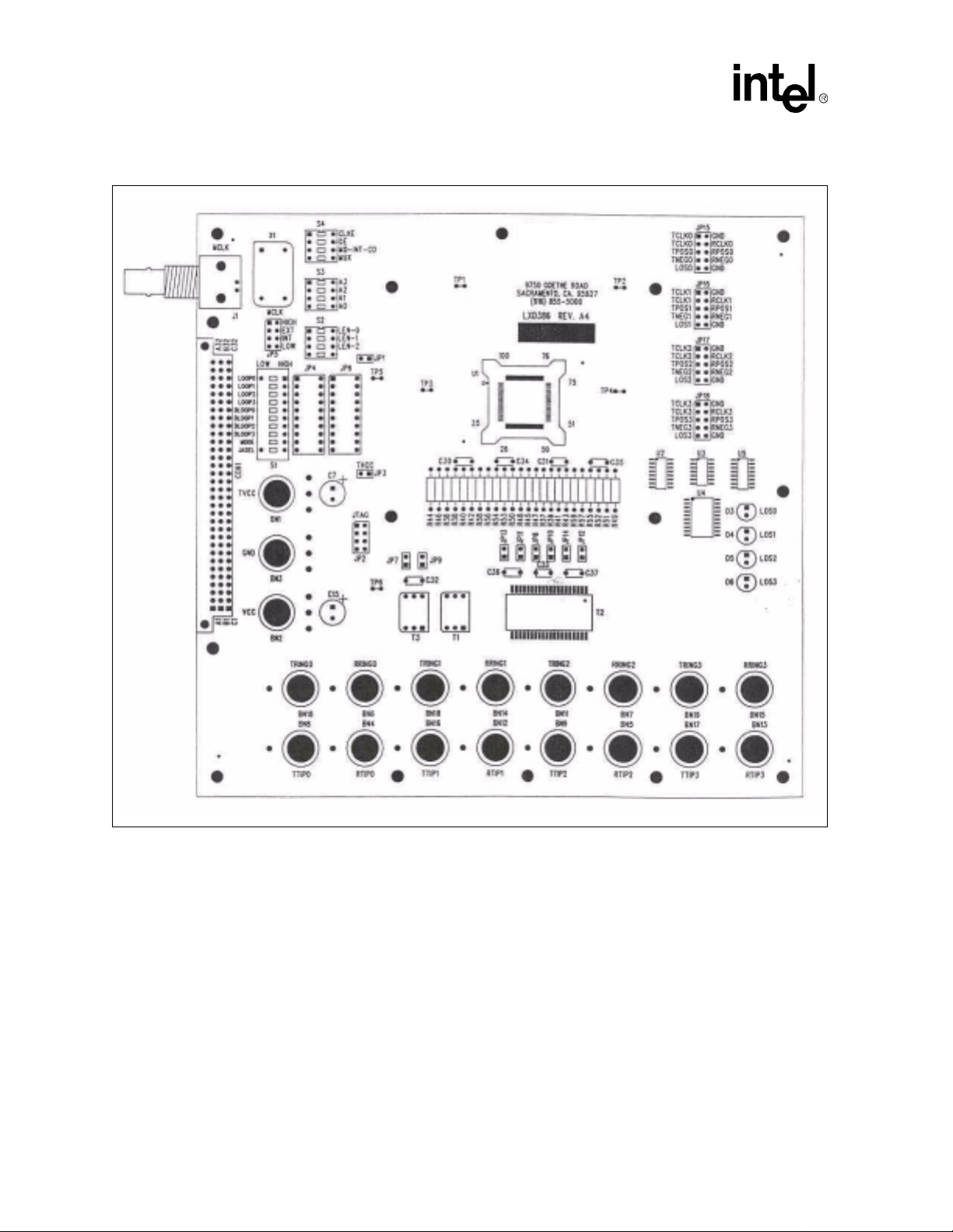
Figure 1. LXD386 Evaluation Board
6 Developer Manual
Page 7

Evaluation Board for Quad T1/E1 Applications — LXD386
2.0 Overview
Caution: CMOS devices are static (ESD) sensitive. Take all industry standard precautions when handling the
evaluation board, LXT386 chip, and other sensitive electronic components.
Before proceeding with any evaluation board operations, review the specifications for the LXT3 86
transceiver.
2.1 LXD386 Packing List
The evaluation board kit contains the following components:
• LXD386 evaluation board with the LXT386 installed.
• 2.048 MHz oscillator installed, additional 1.544 MHz oscillator supplied.
• i8051 microcontroller interface board and PC serial port cable.
• PC compatible diskettes containing software for using the evaluation board in Software mode.
• Shorting block kit for selecting Hardware mode.
• LXD386 user guide.
• LXT386 data sheet.
2.2 Equipment Requirements
The evaluation board kit includes all the circuit components needed for a successful evaluation.
However, the following lab equipment is required:
• Power Supply +3.3V DC (+5VDC for TVCC optional)
• Telecom cable or cable simulator (optional).
• T1/E1 pattern generator/analyzer.
• 1.544/2.048 MHz clock source (optional).
• For Software mode: an IBM compatible PC with minimum 386 40 MHz processor, available
serial po rt, mouse, VGA monitor, DOS 5.0+, and Microsoft Windows
Windows 9x is recommended.
2.3 Control Modes
The LXT386 has two basic operating m odes: Hardware mode or Software (Host ) mode. In
Hardware mode, operation of the LXT386 is established by hard-wiring the pins. In Software
mode, operation of the LXT386 is controlled by an external microprocessor that communicates
with the LXT386’s internal registers via either a serial or parallel interface.
3.1 or later version,
The LXD386 evaluation board supports both hardware and software modes.
Developer Manual 7
Page 8

LXD386 — Evaluation Board for Quad T1/E1 Applications
2.4 Factory Settings
When shipped from the factory, the LXD386 evaluation board’s switches and jumpers are set for
software mode and parallel microprocessor interface.
8 Developer Manual
Page 9

Evaluation Board for Quad T1/E1 Applications — LXD386
3.0 Hardware Mode Set-Up and Operation
3.1 Power Connections
The evaluation board has two power planes (VCC and TVCC) each of which is tied to a separate
red colored banana jack.
1. Connect the +3.3 VDC power supply to the VCC jack.
2. Connect either a +3.3 VDC or +5.0 VDC power supply to the TVCC jack.
3. Connect the power supply ground lead(s) to the black (GND) banana jack.
Jumper JP1 is provided to allow LXT386 current consumption meas urements and must be installed
for normal board operation. Jumper JP3 allows measurement of the current in the TVCC power
supply only. It must also be installed for normal operation.
3.2 Hardware Mode Selection
To enable the Hardware mode of operation:
1. Set the MODE switch in switch block S1 to the LOW position.
2. Insert the two shorting blocks, provided with the evaluation board kit, into 20-pin sock ets JP4
and JP6.
3.3 Loopback Mode Selection
The LXT386 LOOP/DLOOP signals are set by switches in switch block S1. Depending on the
LOOPn/DLOOPn combination selected for a particular channel, a different operation or loopback
mode is selected. Please refer to Table 1.
Table 1. LOOP/DLOOP Switch Settings
LOOPn DLOOPn Channel #n Operation
Open x Normal Mode
LOW x Remote Loopback
HIGH LOW Analog Local Loopback
HIGH HIGH Digital Local Loopback
1. “x” means “don’t care”
3.4 Clock Edge Selection
The phase relation between RCLK and RPOS/RNEG is set by the CLKE switch in switch block
S4. Please refer to the “CLKE” sig nal pin in the LXT386 data sheet for details.
Developer Manual 9
Page 10

LXD386 — Evaluation Board for Quad T1/E1 Applications
3.5 Output Enable Selection
The OE switch in switch block S4 controls the operation of the LXT386 output drivers. For normal
operation (driver outputs enabled), set the OE switch to the ON position. Setting the OE switch to
OFF forces the output drivers to the high impedance state.
3.6 Code Selection
In Hardware mode, the MO-INT-CO switch in switch block S4 selects the line encode/decode. To
select AMI encode/decode set to the ON position. To select B8ZS/HDB3 encode/decode set to the
OFF position.
3.7 Monitoring Address Selection
Switch block S3 sets the Protected Monitoring Addresses A0 throug h A3. The factory defa u lt
setting is 0000 (no monitoring). See the LXT386 data sheet for details.
3.8 Jitter Attenuator Selection
In Hardware mode, the JASEL switch in switch block S1 selects the position of the Jitter
Attenuator in the data path:
• Transmit path = LOW
• Receive path = HIGH
• JA disabled = center
10 Developer Manual
Page 11

Figure 2. Default Switch Settings
Evaluation Board for Quad T1/E1 Applications — LXD386
S3
O
F
F
1 2 3 4
CLKE
OE
MO-INT-CO
MUX
S4
O
F
F
1 2 3 4
A0
A1
A2
A3
S2
O
F
F
1 2 3 4
LEN2
LEN1
LEN0
LOOP0
LOOP1
LOOP2
LOOP3
LOOP4
LOOP5
LOOP6
LOOP7
MODE
JASEL
LOW
S1
HIGH
1 2 3 4
NOTE:
OFF position = Low = ’0’
5 6 7 8 9 10
3.9 Line Buildout Selection
Switch block S2 is used to select the transmit pulse shaping for T1 mode operation, as well as T1/
E1 mode selection. The factory default is 000 (E1 mode). Refer to the LXT386 data sheet for T1
pulse shape details.
3.10 Master Clock Setup
The on-board 2.048 MHz oscillator can be used for MCLK source. An additional 1.544 MHz
oscillator is included for use in T1 operation mo de. A BNC co nnector ( J1 ) is p rov ided to allow us e
of an external MCLK source. J1 is internally terminated into 50
configure MCLK. Table 2 describes the options available with JP5. The factory setup for JP5 sets
internal oscillator timing as illustrated in Figure 3.
T a ble 2. JP5 Jumper Settings
JP5 Setting Operation
HIGH Data recovery mode
EXT External MCLK source at BNC (J1)
INT Internal oscillator
LOW Receiver power-down
Ω. Jumper block JP5 is used to
Developer Manual 11
Page 12

LXD386 — Evaluation Board for Quad T1/E1 Applications
Figure 3. Jumper Block JP5
3.11 JTAG Boundary Scan Port
The eight pin connector JP2 shown in Figure 4 provides access to the IEEE 1149.1 compliant
JTAG boundary scan port for board testing purposes.
Figure 4. Jumper Block JP2
3.12 Framer/ASIC Connection
Ten pin connectors p rovide access to the di gital signals necess ary for interf acing with the back-end
Framer/Mapper or ASIC. Figure 5 represents one of the four connectors with the factory jumper
connecting RCLK to TCLK.
12 Developer Manual
Page 13

Figure 5. Jumper Block JP 31
3.13 LED Indicators
Loss of Signal (LOS) status for each channel is indicated by four LEDs, labeled D3 thro ugh D6. If
the board is being used in the Software mode, the state of these LEDs will also be displayed on the
registers display screen.
Evaluation Board for Quad T1/E1 Applications — LXD386
3.14 Line Interface
Access to the line interface is provided through the green and white banana jacks. The TIP signal
is routed to the white jacks for both transmit and receive directions. The RING signal is routed to
the green jacks for both directions.
An octal transformer is used for channels 1 to 3 (one transformer port is unused). Transformers in
channel 0 and line resistors /capacitors for channels 0 to 3 are socketed for easy swapping. Jumpers
JP7 to JP14 can be used to bypass the transmit series resistors for T1 ap pli cations with
TVCC=3.3V. See the LXT386 Data Sheet for details on transmit interface options.
3.15 Board Protection
The LXD386 evaluation board is equipped with both power supply and line surge protection. Two
Transient Voltage Suppressors (TVS) are included for power supply protection (5V/3.3V). For the
T1/E1 line interface, the transmitters are protected with Schottky diodes and the receivers are
protected by series 1K
compliance.
Ω input resistors. This protection is sufficient for G.703 Annex B
Developer Manual 13
Page 14

LXD386 — Evaluation Board for Quad T1/E1 Applications
4.0 Software Mode Set-Up and Operation
4.1 i8051 Microcontroller Board
An i8051 microcontroller interface board is provided with the evaluation board kit. Connect the
i8051 microcontroller board to the evaluation board at the 96 pin header labeled CON1. Connect
the microcontroller board to an available serial (COM) po rt on your PC u sing the cable prov ided in
the evaluation board kit.
Instead of the i8051, a user supplied microcontroller board may also be used to control the
LXT386. Evaluation board connector CON1 provides access to all the relevant LXT386
microprocessor interface signals.
4.2 Evaluation Board Set-up
The evaluation board contains switches and jumpers to select various operating parameters. All
other parameters are controlled through the evaluation board software. When using the i8051
microcontroller provided with the kit, set the evaluation board switches and jump ers as f oll ows :
1. Select software mode by removing the shorting blocks from sockets JP4 and JP6.
2. Set the MODE switch (in switch block S1) to select serial or parallel mode :
— HIGH for parallel mode (factory default)
— Center position for serial mode
3. Set the JASEL switch (in switch block S1) to the center position.
4. Set MO-INT-CO switch (in switch block S3) to HIGH (Intel microprocessor).
5. Set MUX switch (in switch block S3) to HIGH (Multiplexed microprocessor address/data
bus).
6. Set CLKE switch (in switch block S3). Refer to “CLKE” signal pin in LXT386 data sheet for
details.
7. Set OE switch (in switch block S3) as described in “Output Enable Selection” on page 10.
8. Set the jumper on JP5 as described in “Master Clock Setup” on pag e 11.
4.3 Test Equipment Connections
The evaluation board contains connectors to interface an external pattern generator and other test
equipment. See page 9 for details.
4.4 Power Connections
Connect power supply as described in “Power Connections” on page 9.
14 Developer Manual
Page 15

Evaluation Board for Quad T1/E1 Applications — LXD386
4.5 Evaluation Board Software
When operating the evaluation board in the software mode, the software provided with the kit will
be used to configure the LXT386 and to monitor its operation. This software provides a point-andclick, user friendly interface with on-line help screens. Refer to the data sheet for detailed
information about the LXT386 transceiver.
4.6 Software Installation and Start-Up
The minimum PC system requirements are:
• IBM compatible PC
• 386/40 MHz CPU (Pentium class recommended)
• Available serial port
• Mouse
• VGA monitor
• DOS version 5.0 or higher and Microsoft Windows 3.1 (Windows 9x recommended)
Begin the installation procedure by running the Setup.exe file on the installation diskette #1.
Follow the on-screen prompts to complete the software installation.
4.7 Hardware Set-up Screen
Whenever the LXT386 software is run, the Hardware Set-up screen will appear first on the monitor
(see Figure 6). This screen is used to select the PC serial port to be used. Select an available serial
port and click the OK button.
4.8 Quitting the Program
The program can be terminated at any time by clicking the “Exit” control button, located at the
right side of the screen.
Developer Manual 15
Page 16

LXD386 — Evaluation Board for Quad T1/E1 Applications
Figure 6. Hardware Set-up Screen
4.9 Configuration Screen
The configuration screen shown in Figure 7 is the next screen to appear on the monitor. It is the
primary control interface with the evaluation board. A graphical representation of each channel is
shown in a tabbed display box, along with the control buttons describe d in the following
paragraphs.
4.9.1 Communications Modes
The option buttons located in the communications modes box are used to set the microprocessor
interface mode to parallel interface or serial interface.
Note: The selected communication mode must match the evaluation board MODE switch setting (see
“Evaluation Board Set-up” on page 14). The factory default setting is parallel mode.
4.9.2 Registers
Clicking the Registers control button will select the Registers screen, enabling read/write access to
all the LXT386 registers. See “Registers” on page 16.
4.9.3 Setting Individual Transceiver Operating Modes
Select the transceiver channel you wish to configure b y clicking o n the corr espond ing tab s ymb ol.
Once a channel has been selected, set the operating mode by clicking on one of the three loopback
modes.
16 Developer Manual
Page 17

4.9.4 Apply to all Channels
Clicking the “Apply to All Channels” control button will configure the other three channels to the
settings displayed for the currently selected channel.
4.9.5 Exit
The exit control button can be used at any time to close the software.
Figure 7. Configuration Screen
Evaluation Board for Quad T1/E1 Applications — LXD386
Developer Manual 17
Page 18

LXD386 — Evaluation Board for Quad T1/E1 Applications
4.10 Registers Screen
4.10.1 Setting Registers
The Registers screen (see in Figure 8) allows direct control of all the LXT386 registers. Each
register is labeled by its functional name and hex addres s. Right click on a register na me for on-line
help.
4.10.2 Status Indicators
Display boxes within the Registers screen show the state settings for individual bit positions of
each register. Each of the 4 least significant bits of these registers control the corresponding
transceiver channel, except where otherwise noted in the LXT386 specifications. The check boxes
beside the “Mode” column denote enabling of read/write step modes.
4.10.3 Control Buttons
Clicking on the “Read All” button will initiate a global read of all LXT386 registers. Clicking on
the “Read Step” and “Write Step” buttons performs the indicated action only o n register s that have
the enable box checked. The “Back” button is used to return to the configuration screen, and the
“Exit” control button can be used at any time to close the software.
4.10.4 Interrupts
The Interrupt indicator is located in the lower right corner. This indicator will turn red whenever
there are pending interrupts in the LXT386. Interrupts are cleared by reading the corresponding
Status Monitor register. When all interrupts are cleared, the Interrupt indicator will turn Green. See
Figure 8.
4.10.5 Reset
While operating the evaluation board in Software mode, reset is accomplished by using the write
step function to write to the software reset register address 0Ah.
18 Developer Manual
Page 19

Figure 8. Registers Screen
Evaluation Board for Quad T1/E1 Applications — LXD386
Developer Manual 19
Page 20

LXD386 — Evaluation Board for Quad T1/E1 Applications
5.0 Evaluation Board Schematics
Figure 9. Evaluation Board Schematic — Data/Control
LOS3
LOS2
LOS1
LOS0
JP2
12
34
56
JTAG PORT
TCK
TMS
TDO
TRST
78
HEADER 4X2
AT1
TDI
AT2
of
16Wednesday, September 15, 1999
LEVEL ONE COMMUNICATIONS
DATA/CONTROL A4
FIREBIRD - LXD386 DEMO BOARD
B
Title
Size Document Number Rev
Date: Sheet
R12
100K
R11
100K
CON1C
CON1B
CON1A
LOOP0/D0
LOOP2/D2
DLOOP0/D4A0A2
c30
c31
c32
b30
b31
b32
LOOP1/D1
LOOP3/D3
DLOOP1/D5
a30
a31
a32
DLOOP2/D6
A4
c26
c27
c28
c29
CS
b26
b27
b28
b29
DLOOP3/D7A1A3
a26
a27
a28
a29
CS
OE
829883
ALE/SCLK/AS
CS
OE
OE
CS
INT
ACK/RDY/SDO
DS/WR/SDI
ALE/SCLK/AS
3
80
81
DS/WR/SDI
ACK/RDY/SDO
INT
DS/WR/SDI
ALE/SCLK/AS
7271697370
TDI
TMS
TCK
TDO
TRST
LOOP0/D0
LOOP1/D1
LOOP2/D2
LOOP3/D3
LOOP4/D4
90919293949596
LOOP0/D0
LOOP1/D1
LOOP2/D2
DLOOP0/D4
LOOP3/D3
R10
100K
R9
100K
R8
100K
R7
100K
R6
100K
R5
100K
76
77
AT2
AT1
LOOP5/D5
LOOP6/D6
LOOP7/D7
97
DLOOP2/D6
DLOOP3/D7
DLOOP1/D5
GND_ANA
74
GND_DIG
7
GNDIO
5
GND_3
65
GND_2
66
GND_1
11
GND_0
10
LXT386
251858
51
LOS0
LOS1
LOS2
LOS3
VCC_ANA
VCC
75
VCC_DIG
6
VCCIO
4
VCC_3
67
VCC_2
68
VCC_1
9
VCC_0
8
U1A
MCLK
MODE
CLKE
MUX
MOT/INTL
1
787984
99
CLKE
MCLK
MODE
R4
10K
MOT/INTL
MUX
MOT/INTL
MUX
R/W/RD
A3A2A1
A0
A4
2
89
888786
85
A2
A1
A3
A4
A0
R/W/RD
R/W/RD
C3 .1uF
C4 .1uF
C2 .1uF
C1 .1uF
JP1
VCC
R2
10K
R3
c15
TMS
b15
a15
10K
MODE
VCC
c10
c11
c12
c13
c14
1011121314151617181920212223242526272829303132
INT
TDI
TDO
TCK
b10
b11
b12
b13
b14
1011121314151617181920212223242526272829303132
VCC
a10
a11
a12
a13
a14
1011121314151617181920212223242526272829303132
VCC
R/W/RD
R1
4.7K
c16
c17
c18
c19
c20
c21
c22
c23
c24
c25
TRST
b16
b17
b18
b19
b20
b21
b22
b23
b24
b25
a16
a17
a18
a19
a20
a21
a22
a23
a24
a25
CLKE
DS/WR/SDI
ACK/RDY/SDO
c1c2c3c4c5c6c7c8c9
123456789
b1b2b3b4b5b6b7b8b9
123456789
MUX
ALE/SCLK/AS
MOT/INTL
a1a2a3a4a5a6a7a8a9
123456789
C5 .1uF
C6 .1uF
96 Pin DIN Connector Male
96 Pin DIN Connector Male
96 Pin DIN Connector Male
20 Developer Manual
Page 21

Evaluation Board for Quad T1/E1 Applications — LXD386
Figure 10. Evaluation Board Schematic — Line Interface Unit
TVCC
BN1
1
+
D1
RED
TVS 5V
C9
.1uf
C8
.01uf
C7
68 uF
VCC
BN2
TVS 3.3V
D2
C17
.1uf
C16
C15
68 uF
RED1BN3
.01uf
1
TP6
TESTPOINT
1
TP5
TESTPOINT
1
TP4
TESTPOINT
1
BLACK
-
TP3
TESTPOINT
TP2
TESTPOINT
1
1
of
26Wednesday, September 15, 1999
LEVEL ONE COMMUNICATIONS
LIU A4
FIREBIRD - LXD386 DEMO BOARD
B
Title
Size Document Number Rev
Date: Sheet
BANANA JACK
TVCC
TVCC
BANANA JACK+BANANA JACK
3.3 VOLTS
RTIP0
RRING0
TTIP0
TRING0
272830
31
343337
+
C12 .1uF
C11 .1uF
C13 .1uF
C10 33uF TANT
JP3
TVCCP
C14 .1uF
TTIP0
RTIP0
TRING0
RRING0
TVCC3
47
TVCC2
38
TVCC1
35
TVCC0
26
U1B
TCLK0
TPOS0/TDATA0
TNEG0/UBS0
RCLK0
RPOS0/RDATA0
RNEG0/BPV0
1920212223241213141516176463626160595756555453
TCLK1
TP1
TESTPOINT
RTIP1
RRING1
TTIP1
TRING1
36
TTIP1
RTIP1
TRING1
RRING1
TPOS1/TDATA1
TNEG1/UBS1
RCLK1
RPOS1/RDATA1
RNEG1/BPV1
1
TTIP2
TRING2
394042
TTIP2
TRING2
TCLK2
TPOS2/TDATA2
TNEG2/UBS2
RCLK2
RRING2
RTIP2
TTIP3
464549
43
TTIP3
RTIP2
RRING2
RPOS2/RDATA2
RNEG2/BPV2
TCLK3
TPOS3/TDATA3
RTIP3
RRING3
TRING3
48
RTIP3
TRING3
RRING3
TNEG3/UBS3
RCLK3
RPOS3/RDATA3
RNEG3/BPV3
52
TGND3
44
TGND2
41
TGND1
32
TGND0
29
LXT386
TCLK0
RCLK0
TNEG0/UBS0
RNEG0/BPV0
TPOS0/TDATA0
RPOS0/RDATA0
TCLK1
RCLK1
TNEG1/UBS1
TPOS1/TDATA1
RPOS1/RDATA1
TCLK2
RNEG1/BPV1
TPOS2/TDATA2
RCLK2
TNEG2/UBS2
RNEG2/BPV2
RPOS2/RDATA2
TCLK3
RCLK3
TNEG3/UBS3
TPOS3/TDATA3
RPOS3/RDATA3
RNEG3/BPV3
Developer Manual 21
Page 22

LXD386 — Evaluation Board for Quad T1/E1 Applications
Figure 11. Evaluation Board Schematic — Monitoring
MCLK
JP5
HEADER 4X2
12
34
56
78
VCC
R14 4.7k Ohms
14
VCC
VCC
X
GND C
X1
XTAL
1
7 8
S1
10
7
8
9
R13 50 Ohms
2.048MHZ
6
J1
EXTCLK
BNC
5
EXT. MCLK
VCC
4
R15 50 Ohms
4.7K
R16
TriState10
1 20
2113
DS/WR/SDIA3ALE/SCLK/AS
JP6
12
34
R/W/RD
A2
56
78
910
11 12
13 14
15 16
A1
A0
17 18
19 20
CLKEOEMOT/INTL
HEADER 10X2
MUX
of
36Wednesday, September 15, 1999
LEVEL ONE COMMUNICATIONS
MONITOR A4
FIREBIRD - LXD386 DEMO BOARD
B
Title
Size Document Number Rev
Date: Sheet
R24
4.7k
R23
4.7k
R22
4.7k
R21
4.7k
R20
4.7k
R19
4.7k
R18
4.7k
R17
4.7k
MODE
1920
JP4
HEADER 10X2
SWLOOP7
SWLOOP6
1314
1516
1718
CS
DLOOP2/D6
DLOOP3/D7
SWLOOP4
SWLOOP3
SWLOOP5
1112
DLOOP0/D4
DLOOP1/D5
SWLOOP1
SWLOOP0
SWLOOP2
LOOP2/D2
LOOP3/D3
LOOP1/D1
12345678910
LOOP0/D0
Hardware mode
JA Select
LEN0
876
S2
123
VCC
LINE BUILDOUTS
LEN2
5
4
876
S3
SW DIP-4
123
CLKE
OE
MOT/INT/CODEN
876
SW DIP-4
S4
123
MUX
5
4
SW DIP-4
5
4
PROTECTED MONITORING
ADDRESS SELECT
LEN1
22 Developer Manual
Page 23

Evaluation Board for Quad T1/E1 Applications — LXD386
Figure 12. Evaluation Board Schematic — LOS Detector
VCC
R31
Decoupling
Caps
VCC
C25
.1uf
C21
.1uf
U5U4
C20
.1uf
C19
.1uf
U3U2 X1
C18
.1uf
181614
Y1Y2Y3
U4A
A1A2A3A4G
24681
R32
330 Ohms
330 Ohms
D3
LED YEL.D4LED YEL.D5LED YEL.D6LED YEL.
LOS0
LOS1
12
Y4
74LS240
of
46Wednesday, September 15, 1999
R33
R34
330 Ohms
330 Ohms
LEVEL ONE COMMUNICATIONS
LOS 1 A4
FIREBIRD - LXD386 DEMO BOARD
LOS2
LOS3
B
Title
Size Document Number Rev
Date: Sheet
VCC
3
U3A
74LS32
1
2
13
4
Q
Q
U2A
CEXT
14
C26
47uF TANT
+
R28
25K
REXT/CEXTAB
15
123
LOS0
CLR
74LS221
VCC
U2B
6
CEXT
C27
+
R29
25K
U3B
REXT/CEXTAB
7
47uF TANT
6
74LS32
4
5
5
12
Q
Q
74LS221
U5A
CLR
9
10
11
LOS1
14
VCC
CEXT
C28
47uF TANT
+
R30
25K
U3C
REXT/CEXTAB
15
9
13
123
8
74LS32
10
4
Q
Q
74LS221
U5B
CLR
LOS2
6
VCC
CEXT
C29
+
R35
25K
U3D
REXT/CEXTAB
7
47uF TANT
11
74LS32
12
13
5
12
Q
Q
74LS221
CLR
9
10
11
LOS3
Developer Manual 23
Page 24

LXD386 — Evaluation Board for Quad T1/E1 Applications
Figure 13. Evaluation Board Schematic — Analog
TVCC
JP11
GREEN
BN16
1
TTIP1x
242523
T2D
R56
11 Ohms
D15
D17
TTIP1
C36 560pF
TVCC
WHITE
BN18
1
TRING1x
21
22
TG-49-1505-NX
1920181716
11 Ohms
JP13
R58
D19
D21
TRING1
BN4
R36
1
RTIP0x
RTIP0
1K
GREEN
R38
T1
6
15 Ohms
C30
.22uF
153
2
R40
BN6
1
RRING0x
PE-65351
15 Ohms
R42
TVCC
RRING0
WHITE
1:2CT
JP7
1K
D7
BN8
GREEN
1
TTIP0x
T3
6
R44
11 Ohms
D9
TTIP0
C32 560pF
TVCC
153
2
D11
BN10
1
TRING0x
PE-65351
R46
11 Ohms
TRING0
WHITE
1:2CT
D13
LEVEL ONE COMMUNICATIONS
JP9
of
56Wednesday, September 15, 1999
ANALOG A4
FIREBIRD - LXD386 DEMO BOARD
B
Title
Size Document Number Rev
Date: Sheet
T2B
C37
11 Ohms
D18
BN17
560pF
D20
GREEN
1
TTIP3x
R59
WHITE
BN19
1
TRING3x
343533
TRING3
BN7
32
910876
11 Ohms
D22
WHITE
1
RRING2x
31
JP14
GREEN
BN5
1
RTIP2x
TG-49-1505-NX
R41
C31
R43
1K
RRING2
15 Ohms
WHITE
GREEN
WHITE
1
TRING2x
560pF
R45
BN9
1
TTIP2x
293028
TTIP2
1415131211
JP8
D10
GREEN
BN12
1
RTIP1x
26
27
11 Ohms
BN14
1
RRING1x
TG-49-1505-NX
R48
RTIP1
R53
R50
15 Ohms
15 Ohms
R54
1K
1K
C34
.22uF
RRING1
BN11
T2C
C33
R39
.22uF
R37
15 Ohms
RTIP2
JP10
R47
11 Ohms
D12
D14
TVCC
1K
D8
TVCC
TRING2
WHITE
GREEN
BN15
BN13
1
1
RTIP3x
RRING3x
36
37
394038
T2A
R51
15 Ohms
C35
R49
1K
RTIP3
45321
R52
.22uF
15 Ohms
R55
RRING3
TG-49-1505-NX
JP12
1K
D16
TVCC
R57
TVCC
TTIP3
24 Developer Manual
Page 25

Evaluation Board for Quad T1/E1 Applications — LXD386
Figure 14. Evaluation Board Schematic — Digital I/O
of
66Wednesday, September 15, 1999
LEVEL ONE COMMUNICATIONS
DIGITAL I/O A4
FIREBIRD - LXD386 DEMO BOARD
B
Title
Size Document Number Rev
Date: Sheet
RPOS0/RDATA0
RCLK0
JP15
12
34
56
TCLK0
TPOS0/TDATA0
RNEG0/BPV0
CHANNEL 0
78
910
HEADER 5X2
R62
R61
R60
LOS0
TNEG0/UBS0
100k
100k
100k
RPOS1/RDATA1
RCLK1
JP16
12
34
56
TCLK1
TPOS1/TDATA1
RNEG1/BPV1
CHANNEL 1
78
910
HEADER 5X2
R65
R64
R63
LOS1
TNEG1/UBS1
100k
100k
100k
RCLK2
RPOS2/RDATA2
JP17
12
34
56
TCLK2
TPOS2/TDATA2
RNEG2/BPV2
CHANNEL 2
78
910
HEADER 5X2
R68
R67
R66
LOS2
TNEG2/UBS2
100k
100k
100k
RCLK3
RPOS3/RDATA3
JP18
12
34
56
TCLK3
TPOS3/TDATA3
RNEG3/BPV3
CHANNEL 3
78
910
HEADER 5X2
R71
R70
R69
LOS3
TNEG3/UBS3
100k
100k
100k
Developer Manual 25
Page 26

 Loading...