

Page 1

R
Intel® 820E Chipset
Design Guide
May 2001
Document Number: 298187-003
Page 2

Intel® 820E Chipset
A
y
R
Information in this document is provided in connection with Intel® products. No license, express or implied, by estoppel or otherwise, to any intellectual
property rights is granted by this document. Except as provided in Intel’s Terms and Conditions of Sale for such products, Intel assumes no liability
whatsoever, and Intel disclaims any express or implied warranty, relating to sale and/or use of Intel products including liability or warranties relating to fitness
for a particular purpose, merchantability, or infringement of any patent, copyright or other intellectual property right. Intel products are not intended for use in
medical, life saving, or life sustaining applications.
Intel may make changes to specifications and product descriptions at any time, without notice.
Designers must not rely on the absence or characteristics of any features or instructions marked "reserved" or "undefined." Intel reserves these for future
definition and shall have no responsibility whatsoever for conflicts or incompatibilities arising from future changes to them.
®
The Intel
Current characterized errata are available on request.
Contact your local Intel sales office or your distributor to obtain the latest specifications and before placing your product order.
I
Implementations of the I
Corporation.
Copies of documents that have an ordering number and are referenced in this document, or other Intel literature, may be obtained from:
www.intel.com
or call 1-800-548-4725
Intel, Pentium III, Pentium II, PentiumPro, Celeron, and MMX are trademarks or registered trademarks of Intel Corporation or its subsidiaries in the United
States and other countries.
*Other names and brands ma
820E Chipset may contain design defects or errors known as errata which may cause the product to deviate from published specifications.
2
C is a two-wire communications bus/protocol developed by Philips. SMBus is a subset of the I2C bus/protocol and was developed by Intel.
lert on LAN is a result of the Intel-IBM Advanced Manageability Alliance and a trademark of IBM
Intel Corporation
2
C bus/protocol may require licenses from various entities, including Philips Electronics N.V. and North American Philips
be claimed as the property of others.
2 Design Guide
Page 3

Intel® 820E Chipset
R
Contents
Introduction ................................................................................................................................ 13
1.
1.1. About This Design Guide .............................................................................................. 13
1.2. Reference Documents................................................................................................... 14
1.3. System Overview........................................................................................................... 15
1.3.1. Chipset Components................................................................................... 16
1.3.2. Bandwidth Summary ................................................................................... 17
1.3.3. System Configuration .................................................................................. 18
1.4. Platform Initiatives ......................................................................................................... 20
1.4.1. Direct Rambus RAM (RDRAM*) ................................................................. 20
1.4.2. Streaming SIMD Extensions ....................................................................... 20
1.4.3. AGP 2.0....................................................................................................... 20
1.4.4. Hub Interface............................................................................................... 20
1.4.5. Integrated LAN Controller............................................................................ 21
1.4.6. Ultra ATA/100 Support ................................................................................ 21
1.4.7. Expanded USB Support .............................................................................. 21
1.4.8. Manageability .............................................................................................. 21
1.4.9. AC’97 ........................................................................................................ 23
1.4.10. Low-Pin-Count (LPC) Interface ................................................................... 25
2. Layout/Routing Guidelines ......................................................................................................... 27
2.1. General Recommendations........................................................................................... 27
2.2. Component Quadrant Layout ........................................................................................ 27
2.3. Intel® 820E Chipset Component Placement.................................................................. 29
2.4. Core Chipset Routing Recommendations ..................................................................... 30
2.5. Source-Synchronous Strobing....................................................................................... 32
2.6. Differential Clocking/Strobing ........................................................................................ 33
2.7. Direct RDRAM* Interface .............................................................................................. 33
2.7.1. Stack-Up...................................................................................................... 34
2.7.2. Direct RDRAM* Layout Guidelines.............................................................. 34
2.7.2.1. RSL Routing ................................................................................... 35
2.7.2.2. RSL Termination............................................................................. 38
2.7.2.3. Direct RDRAM* Ground Plane Reference...................................... 39
2.7.2.4. Direct RDRAM* Connector Compensation..................................... 41
2.7.2.4.1. Direct RDRAM* Channel Connector Compensation
Enhancement Recommendation .................................. 47
2.7.2.5. RSL Signal Layer Alternation.......................................................... 49
2.7.2.6. Length Matching Methods .............................................................. 50
2.7.2.7. Via Compensation .......................................................................... 52
2.7.2.8. Length Matching and Via Compensation Example......................... 52
2.7.3. Direct RDRAM* Reference Voltage............................................................. 54
2.7.4. High-Speed CMOS Routing ........................................................................ 54
2.7.4.1. SIO Routing .................................................................................... 55
2.7.4.2. Suspend-to-RAM Shunt Transistor................................................. 56
2.7.5. Direct RDRAM* Clock Routing .................................................................... 57
2.7.6. Direct RDRAM* Design Checklist ............................................................... 57
2.8. AGP 2.0 .........................................................................................................................60
2.8.1. AGP Interface Signal Groups ...................................................................... 60
2.8.2. 1× Timing Domain Routing Guidelines........................................................ 62
Design Guide 3
Page 4

Intel® 820E Chipset
R
2.8.3.
2×/4× Timing Domain Routing Guidelines ...................................................62
2.8.4. AGP 2.0 Routing Summary .........................................................................64
2.8.5. AGP Clock Routing ...................................................................................... 65
2.8.6. General AGP Routing Guidelines ................................................................65
2.8.6.1. Recommendations ..........................................................................65
2.8.7. V
2.8.8. V
Generation and TYPEDET# ................................................................ 66
DDQ
Generation for AGP 2.0 (2× and 4×).................................................... 68
REF
2.8.9. Compensation.............................................................................................. 70
2.8.10. AGP Pull-Ups...............................................................................................70
2.8.10.1. AGP Signal Voltage Tolerance List ................................................. 71
2.8.11. Motherboard / Add-in Card Interoperability..................................................71
2.8.12. AGP Universal Retention Mechanism (RM) ................................................ 72
2.9. Hub Interface .................................................................................................................74
2.9.1. 8-Bit Hub Interface Routing Guidelines .......................................................75
2.9.1.1. 8-Bit Hub Interface Data Signals..................................................... 75
2.9.1.2. 8-Bit Hub Interface Strobe Signals.................................................. 75
2.9.1.3. 8-Bit Hub Interface HUBREF Generation/Distribution..................... 75
2.9.1.4. 8-Bit Hub Interface Compensation ..................................................77
2.9.1.5. 8-Bit Hub Interface Decoupling Guidelines .....................................77
2.10. System Bus Design – Pentium® III Processor for the Intel® PGA370 Socket Layout
Guidelines ......................................................................................................................77
2.10.1. System Bus Ground Plane Reference ......................................................... 78
2.11. Additional Host Bus Guidelines...................................................................................... 78
2.12. IDE Interface ..................................................................................................................79
2.12.1. Cable Detection for Ultra ATA/66 and Ultra ATA/100..................................80
2.12.2. Combination Host-Side/Device-Side Cable Detection ................................. 80
2.12.3. Device-Side Cable Detection ....................................................................... 82
2.12.4. Primary IDE Connector Requirements ........................................................83
2.12.5. Secondary IDE Connector Requirements....................................................84
2.13. AC’97 .............................................................................................................................85
2.13.1. AC’97 Audio Codec Detect Circuit and Configuration Options ....................86
2.13.2. Communication and Networking Riser (CNR) .............................................90
2.13.3. AC’97 Routing..............................................................................................91
2.13.4. Motherboard Implementation ....................................................................... 92
2.14. USB................................................................................................................................92
2.14.1. Using Native USB Interface .........................................................................92
2.14.3. Disabling the Native USB Interface of ICH2 ................................................93
2.15. ISA Support....................................................................................................................93
2.16. I/O APIC Design Recommendation ...............................................................................94
2.17. SMBus/SMLink Interface ...............................................................................................94
2.18. PCI .................................................................................................................................96
2.19. RTC................................................................................................................................96
2.19.1. RTC Crystal .................................................................................................97
2.19.2. External Capacitors .....................................................................................97
2.19.3. RTC Layout Considerations......................................................................... 98
2.19.4. RTC External Battery Connection................................................................98
2.19.5. RTC External RTCRST Circuit ....................................................................99
2.19.6. RTC Routing Guidelines ............................................................................100
2.19.7. VBIAS DC Voltage and Noise Measurements ...........................................100
2.19.8. RTC-Well Input Strap Requirements .........................................................100
2.20. SPKR Pin Consideration ..............................................................................................100
2.21. ICH2 PIRQ Routing......................................................................................................101
4 Design Guide
Page 5

Intel® 820E Chipset
R
2.22.
LAN Layout Guidelines ................................................................................................ 102
2.22.1. ICH2 – LAN Interconnect Guidelines ........................................................ 103
2.22.1.1. Bus Topologies ............................................................................. 104
2.22.1.2. Point-to-Point Interconnect ........................................................... 104
2.22.1.3. LOM/CNR Interconnect ................................................................ 104
2.22.1.4. Signal Routing and Layout............................................................ 105
2.22.1.5. Crosstalk Consideration ............................................................... 106
2.22.1.6. Impedances .................................................................................. 106
2.22.1.7. Line Termination ........................................................................... 106
2.22.2. General LAN Routing Guidelines and Considerations .............................. 107
2.22.2.1. General Trace Routing Considerations ........................................ 107
2.22.2.1.1. Trace Geometry and Length....................................... 108
2.22.2.1.2. Signal Isolation ........................................................... 108
2.22.2.2. Power and Ground Connections .................................................. 108
2.22.2.2.1. General Power and Ground Plane Considerations .... 108
2.22.2.3. 4-Layer Board Design................................................................... 110
2.22.3. Intel® 82562EH Home/PNA* Guidelines ................................................... 112
2.22.3.1. Power and Ground Connections .................................................. 112
2.22.3.2. Guidelines for Intel® 82562EH Component Placement ................ 112
2.22.3.3. Crystals and Oscillators ................................................................ 112
2.22.3.4. Phoneline HPNA Termination....................................................... 113
2.22.3.5. Critical Dimensions ....................................................................... 114
2.22.3.5.1. Distance from Magnetics Module to Line RJ11.......... 114
2.22.3.5.2. Distance from Intel® 82562EH Component to
Magnetics Module ...................................................... 114
2.22.3.5.3. Distance from LPF to Phone RJ11 ............................. 115
2.22.4. Intel® 82562ET / Intel® 82562EM Component Guidelines......................... 115
2.22.4.1. Guidelines for Intel® 82562ET / Intel® 82562EM Component
Placement .................................................................................... 115
2.22.4.2. Crystals and Oscillators ................................................................ 116
2.22.4.3. Intel® 82562ET / Intel® 82562EM Component Termination
Resistors .................................................................................... 116
2.22.4.4. Critical Dimensions ....................................................................... 116
2.22.4.4.1. Distance from Magnetics Module to RJ45.................. 117
2.22.4.4.2. Distance from the Intel® 82562ET Component to the
Magnetics Module ...................................................... 118
2.22.4.5. Reducing Circuit Inductance......................................................... 118
2.22.4.6. Terminating Unused Connections ................................................ 118
2.22.4.6.1. Termination Plane Capacitance ................................. 118
2.22.5. Intel® 82562ET/EM Disable Guidelines ....................................................... 119
2.22.6. Intel® 82562ET and Intel® 82562EH Components’ Dual-Footprint
Guidelines.................................................................................................... 120
2.22.7. ICH2 Decoupling Recommendations ........................................................ 122
2.23. FWH Flash BIOS Guidelines....................................................................................... 124
2.23.1. In-Circuit FWH Flash BIOS Programming ................................................ 124
2.23.2. FWH Flash BIOS VPP Design Guidelines ................................................ 124
2.24. ICH2 Design Checklist ................................................................................................ 125
2.25. ICH2 Layout Checklist ................................................................................................. 134
3. Advanced System Bus Design................................................................................................. 139
3.1. Terminology and Definitions ........................................................................................ 139
3.2. AGTL+ Design Guidelines........................................................................................... 141
3.2.1. Initial Timing Analysis................................................................................ 142
3.2.2. Determine the Desired General Topology, Layout, and Routing............... 145
Design Guide 5
Page 6

Intel® 820E Chipset
R
3.2.3.
Pre-Layout Simulation................................................................................145
3.2.3.1. Methodology.................................................................................. 145
3.2.3.2. Sensitivity Analysis........................................................................145
3.2.3.3. Monte Carlo Analysis ....................................................................146
3.2.3.4. Simulation Criteria......................................................................... 146
3.2.4. Place and Route Board..............................................................................147
3.2.4.1. Estimate Component-to-Component Spacing for AGTL+ Signals 147
3.2.4.2. Layout and Route Board ...............................................................147
3.2.4.3. Host Clock Routing .......................................................................148
3.2.4.4. APIC Data Bus Routing................................................................. 148
3.2.5. Post-Layout Simulation .............................................................................. 149
3.2.5.1. Intersymbol Interference ...............................................................149
3.2.5.2. Crosstalk Analysis......................................................................... 150
3.2.5.3. Monte Carlo Analysis ....................................................................150
3.2.6. Validation ...................................................................................................150
3.2.6.1. Measurements ..............................................................................150
3.2.6.2. Flight Time Simulation................................................................... 150
3.2.6.3. Flight Time Hardware Validation ...................................................151
3.3. Theory..........................................................................................................................152
3.3.1. AGTL+ ......................................................................................................152
3.3.2. Timing Requirements................................................................................. 152
3.3.3. Crosstalk Theory........................................................................................ 153
3.3.3.1. Potential Termination Crosstalk Problems....................................154
3.4. More Details and Insight ..............................................................................................155
3.4.1. Textbook Timing Equations .......................................................................155
3.4.2. Effective Impedance and Tolerance/Variation ...........................................156
3.4.3. Power/Reference Planes, PCB Stack-Up, and High-Frequency
Decoupling .................................................................................................156
3.4.3.1. Power Distribution .........................................................................156
3.4.3.2. Reference Planes and PCB Stack-Up ..........................................157
3.4.3.3. High-Frequency Decoupling.......................................................... 159
3.4.4. Clock Routing ............................................................................................160
3.5. Definitions of Flight Time Measurements/Corrections and Signal Quality...................160
3.5.1. V
Guard Band .......................................................................................161
REF
3.5.2. Ringback Levels ........................................................................................161
3.5.3. Overdrive Region....................................................................................... 161
3.5.4. Flight Time Definition and Measurement ................................................... 162
3.6. Conclusion ...................................................................................................................162
4. Clocking .................................................................................................................................... 163
4.1. Clock Generation .........................................................................................................163
4.2. Component Placement and Interconnection Layout Requirements ............................168
4.2.1. 14.318 MHz Crystal to CK133 ...................................................................168
4.2.2. CK133 to DRCG ........................................................................................168
4.2.3. MCH to DRCG ...........................................................................................169
4.2.4. DRCG-to-RDRAM Channel .......................................................................170
4.2.5. Trace Length.............................................................................................. 170
4.3. DRCG Impedance Matching Circuit.............................................................................172
4.3.1. DRCG Layout Example..............................................................................173
4.4. AGP Clock Routing Guidelines ....................................................................................173
4.5. Clock Routing Guidelines for Intel® PGA370 Designs..................................................173
4.6. Series Termination Resistors for CK133 Clock Outputs.............................................. 173
4.7. Unused Outputs ...........................................................................................................174
6 Design Guide
Page 7

Intel® 820E Chipset
R
4.8.
Decoupling Recommendation for CK133 and DRCG ................................................. 174
4.9. DRCG Frequency Selection and the DRCG+ ............................................................. 175
4.9.1. DRCG Frequency Selection Table and Jitter Specification....................... 175
4.9.2. DRCG+ Frequency Selection Schematic .................................................. 176
5. System Manufacturing ............................................................................................................. 177
5.1. Stack-Up Requirement ................................................................................................ 177
5.1.1. PCB Materials ........................................................................................... 177
5.1.2. Design Process ......................................................................................... 178
5.1.3. Test Coupon Design Guidelines................................................................ 178
5.1.4. Recommended Stack-Up .......................................................................... 179
5.1.5. Inner-Layer Routing................................................................................... 179
5.1.6. Impedance Calculation Tools .................................................................... 180
5.1.7. Testing Board Impedance ......................................................................... 181
5.1.8. Board Impedance/Stack-up Summary ...................................................... 181
6. System Design Considerations ................................................................................................ 183
6.1. Power Delivery............................................................................................................. 183
6.1.1. Terminology and Definitions...................................................................... 183
6.1.2. Power Delivery of Intel® 820E Chipset Customer Reference Board ......... 184
6.1.3. ICH2 1.8 V / 3.3 V Power Sequencing ...................................................... 188
6.1.5. Excessive Power Consumption by 64/72-Mbit RDRAM............................ 190
6.1.5.1. Option 1: Reduce the Clock Frequency During Initialization ........ 190
6.1.5.2. Option 2: Increase the Current Capability of the 2.5 V Voltage
Regulator ...................................................................................... 191
6.2. ICH2 Power Plane Split ............................................................................................... 192
6.3. Thermal Design Power ................................................................................................ 193
6.4. Glue Chip 3 (Intel® 820E Chipset Glue Chip) .............................................................. 193
Appendix A: Reference Design Schematics (Uniprocessor) ........................................................................... 195
Design Guide 7
Page 8

Intel® 820E Chipset
R
Figures
Figure 1. Intel® 820E Chipset Platform Performance Desktop Block Diagram ........................18
Figure 2. Intel® 820E Chipset Platform Performance Desktop Block Diagram
(with ISA Bridge)........................................................................................................18
Figure 3. Intel® 820E Chipset Platform Dual-Processor Performance Desktop Block
Diagram.....................................................................................................................19
Figure 4. (A-C) AC’97 Connections ..........................................................................................24
Figure 5. MCH 324-Ball µBGA* CSP Quadrant Layout (Top View) .........................................28
Figure 6. ICH2 360-Ball EBGA Quadrant Layout (Top View) ...................................................28
Figure 7. Sample ATX and NLX MCH/ICH2 Component Placement .......................................29
Figure 8. Primary-Side MCH Core Routing Example (ATX).....................................................30
Figure 9. Secondary-Side MCH Core Routing Example (ATX) ................................................31
Figure 10. Data Strobing Example ...........................................................................................32
Figure 11. Effect of Crosstalk on Strobe Signal .......................................................................32
Figure 12. RIMM Diagram ........................................................................................................33
Figure 13. RSL Routing Dimensions ........................................................................................35
Figure 14. RSL Routing Diagram .............................................................................................36
Figure 15. Primary-Side RSL Breakout Example .....................................................................36
Figure 16. Secondary-Side RSL Breakout Example ................................................................37
Figure 17. Direct RDRAM Termination.....................................................................................38
Figure 18. Direct RDRAM* Termination Example ....................................................................39
Figure 19. Incorrect Direct RDRAM* Ground Plane Referencing.............................................40
Figure 20. Direct RDRAM* Ground Plane Reference...............................................................40
Figure 21. Connector Compensation Example ........................................................................43
Figure 22. Section A (See Note), Top Layer.............................................................................44
Figure 23. Section A (See Note), Bottom Layer .......................................................................45
Figure 24. Section B (See Note), Top Layer.............................................................................46
Figure 25. Section B (See Note), Bottom Layer .......................................................................47
Figure 26. Top-Layer CTAB with RSL Signal Routed on the Same Layer (C
= 0.8 pF) ......48
EFF
Figure 27. Bottom-Layer CTAB with RSL Signal Routed on the Same Layer
(C
= 1.35 pF).......................................................................................................48
EFF
Figure 28. Bottom-Layer CTABs Split across the Top and Bottom Layer to Achieve an
Effect C
~1.35 pF...............................................................................................49
EFF
Figure 29. RSL Signal Layer Alternation ..................................................................................50
Figure 30. Example of RDRAM Trace Length Matching ..........................................................51
Figure 31. “Dummy” Via vs. “Real” Via.....................................................................................52
Figure 32. RAMREF Generation Example Circuit ....................................................................54
Figure 33. High-Speed CMOS Termination..............................................................................55
Figure 34. SIO Routing Example ..............................................................................................55
Figure 35. RDRAM CMOS Shunt Transistor ............................................................................56
Figure 36. AGP 2×/4× Routing Example for Interfaces < 6 Inches ..........................................63
Figure 37. Top Signal Layer .....................................................................................................66
Figure 38. AGP V
Figure 39. AGP 2.0 V
Generation Example Circuit ...................................................................68
DDQ
Generation and Distribution ..............................................................69
REF
Figure 40. AGP Left-Handed Retention Mechanism ................................................................72
Figure 41. AGP Left-Handed RM Keep-Out Information..........................................................73
Figure 42. Hub Interface Signal Routing Example ...................................................................74
Figure 43. 8-Bit Hub Interface with a Shared Reference Divider Circuit
(Normal/Single Mode) .............................................................................................76
Figure 44. 8-Bit Hub Interface with Locally Generated Reference Divider Circuits
(Normal/Local Mode) ...............................................................................................76
Figure 45. Ground Plane Reference (4-Layer Motherboard)....................................................78
Figure 46. Combination Host-Side/Device-Side IDE Cable Detection .....................................81
8 Design Guide
Page 9

Intel® 820E Chipset
R
Figure 47. Device-Side IDE Cable Detection ........................................................................... 82
Figure 48. Connection Requirements for Primary IDE Connector ........................................... 83
Figure 49. Connection Requirements for Secondary IDE Connector ...................................... 84
Figure 50. ICH2 AC’97– Codec Connection ............................................................................ 85
Figure 51. CDC_DN_ENAB# Support Circuitry for a Single Codec on Motherboard ............... 87
Figure 52. CDC_DN_ENAB# Support Circuitry for Multi-Channel Audio Upgrade .................. 88
Figure 53. CDC_DN_ENAB# Support Circuitry for Two-Codecs on Motherboard /
One-Codec on CNR................................................................................................ 88
Figure 54. CDC_DN_ENAB# Support Circuitry for Two-Codecs on Motherboard /
Two-Codecs on CNR.............................................................................................. 89
Figure 55. CNR Interface ......................................................................................................... 90
Figure 56. USB Data Signals ................................................................................................... 93
Figure 57. SMBUS/SMLink Interface ....................................................................................... 95
Figure 58. PCI Bus Layout Example ........................................................................................ 96
Figure 59. External Circuitry for the ICH RTC2........................................................................ 97
Figure 60. Diode Circuit Connecting RTC External Battery .....................................................98
Figure 61. RTCRST External Circuit for ICH2 RTC................................................................. 99
Figure 62. SPKR Circuit ......................................................................................................... 101
Figure 63. Example PCI IRQ Routing .................................................................................... 102
Figure 64. ICH2 / LAN Connect Section ................................................................................ 103
Figure 65. Single-Solution Interconnect ................................................................................. 104
Figure 66. LOM/CNR Interconnect ........................................................................................ 105
Figure 67. LAN_CLK Routing Example.................................................................................. 106
Figure 68. Trace Routing ....................................................................................................... 107
Figure 69. Ground Plane Separation ..................................................................................... 109
Figure 70. Intel® 82562EH Component Termination.............................................................. 113
Figure 71. Critical Dimensions for Component Placement .................................................... 114
Figure 72. Intel® 82562ET/82562EM Component Termination.............................................. 116
Figure 73. Critical Dimensions for Component Placement .................................................... 117
Figure 74. Termination Plane................................................................................................. 119
Figure 75. Intel® 82562ET/EM Disable Circuit ....................................................................... 119
Figure 76. Dual-Footprint LAN Connect Interface.................................................................. 120
Figure 77. Dual-Footprint Analog Interface ............................................................................ 121
Figure 78. Decoupling Capacitor Layout................................................................................ 123
Figure 79. One Signal Layer and One Reference Plane........................................................ 157
Figure 80. Layer Switch with One Reference Plane .............................................................. 157
Figure 81. Layer Switch with Multiple Reference Planes (Same Type) ................................. 158
Figure 82. Layer Switch with Multiple Reference Planes ....................................................... 158
Figure 83. One Layer with Multiple Reference Planes........................................................... 159
Figure 84. Overdrive Region and V
Guard Band............................................................... 161
REF
Figure 85. Rising-Edge Flight Time Measurement ................................................................ 162
Figure 86. Intel® 820E Chipset Platform Clock Distribution.................................................... 164
Figure 87. Intel® 820E Chipset Clock Routing Guidelines
1,2
.................................................. 166
Figure 88. CK133-to-DRCG Routing Diagram....................................................................... 168
Figure 89. MCH-to-DRCG Routing Diagram.......................................................................... 169
Figure 90. Direct RDRAM* Clock Routing Dimensions.......................................................... 169
Figure 91. Differential Clock Routing Diagram (Sections A, C & D) ...................................... 171
Figure 92. Non-Differential Clock Routing Diagram (Section B) ............................................ 171
Figure 93. Termination for Direct RDRAM* Clocking Signals CFM/CFM# ............................ 171
Figure 94. DRCG Impedance Matching Network................................................................... 172
Figure 95. DRCG Layout Example......................................................................................... 173
Figure 96. DRCG+ Frequency Selection................................................................................ 176
Figure 97. 28 Ω Trace Geometry ........................................................................................... 177
Figure 98. Microstrip (a) and Stripline (b) Cross Section for 28 Ω Trace............................... 180
Figure 99. 7 mil Stack-Up (Not Routable) .............................................................................. 181
Design Guide 9
Page 10

Intel® 820E Chipset
R
Tables
Figure 100. 4.5 mil Stack-Up ..................................................................................................181
Figure 101. Intel® 820E Chipset Power Delivery Example......................................................184
Figure 102. 1.8 V and 2.5 V Power Sequencing (Schottky Diode) .........................................187
Figure 103. Example 1.8V/3.3V Power Sequencing Circuit ...................................................189
Figure 104. Example 3.3V/5V REF Sequencing Circuitry ......................................................190
Figure 105. Use a GPO to Reduce DRCG Frequency ...........................................................191
Figure 106. Example of ICH2 Power Plane Split ....................................................................192
Table 1. Intel® 820E Chipset Platform Bandwidth Summary ....................................................17
Table 2. AGP 2× Data/Strobe Association ...............................................................................33
Table 3. Placement Guidelines for Motherboard Routing Lengths...........................................35
Table 4. Copper Tab Area Calculation .....................................................................................42
Table 5. RSL and Clocking Signal RIMM Connector Capacitance Recommendations ...........47
Table 6. Copper Tab Area Calculation .....................................................................................48
Table 7. RSL Routing Layer Requirements ..............................................................................50
Table 8. Line Matching and Via Compensation Example.........................................................53
Table 9. Signal List ...................................................................................................................57
Table 10. AGP 2.0 Data/Strobe Associations...........................................................................62
Table 11. AGP 2.0 Routing Summary ......................................................................................64
Table 12. TYPDET#/V
Relationship ....................................................................................67
DDQ
Table 13. Connector / Add-in Card Interoperability ..................................................................71
Table 14. Voltage / Data Rate Interoperability..........................................................................71
Table 15. 8-Bit Hub Interface Buffer Configuration Setting ......................................................75
Table 16. 8-Bit Hub Interface HUBREF Generation Circuit Specifications ..............................76
Table 17. 8-Bit Hub Interface RCOMP Resistor Values ...........................................................77
Table 18. Signal Descriptions...................................................................................................89
Table 19. Codec Configurations ...............................................................................................90
Table 20. Pull-Up Requirements for SMBus and SMLink Signals............................................95
Table 21. Usage of I/O APIC Interrupt Inputs 16 through 23..................................................101
Table 22. LAN Design Guide Section Reference ...................................................................103
Table 23. Length Requirements for Figure 66........................................................................105
Table 24. Related Documents ................................................................................................112
Table 25. Decoupling Capacitor Recommendation ................................................................122
Table 26. PCI Interface...........................................................................................................125
Table 27. Hub Interface ..........................................................................................................126
Table 28. LAN Interface..........................................................................................................126
Table 29. EEPROM Interface .................................................................................................126
Table 30. FWH Flash BIOS Interface.....................................................................................126
Table 31. Interrupt Interface ...................................................................................................127
Table 32. GPIO.......................................................................................................................128
Table 33. USB Interface .........................................................................................................128
Table 34. Power Management ...............................................................................................129
Table 35. Processor Signals...................................................................................................129
Table 36. System Management..............................................................................................130
Table 37. RTC ........................................................................................................................130
Table 38. AC’97 ......................................................................................................................130
Table 39. Miscellaneous Signals ............................................................................................131
Table 40. Power......................................................................................................................131
Table 41. IDE Checklist ..........................................................................................................132
Table 42. ISA Bridge Checklist ...............................................................................................133
Table 43. 8-Bit Hub Interface..................................................................................................134
Table 44. IDE Interface...........................................................................................................134
10 Design Guide
Page 11

Intel® 820E Chipset
R
Table 45. USB........................................................................................................................ 134
Table 46. LAN Connect I/F..................................................................................................... 135
Table 47. AC’97 ..................................................................................................................... 136
Table 48. ICH2 Decoupling .................................................................................................... 136
Table 49. CK-SKS Clocking ................................................................................................... 137
Table 50. RTC........................................................................................................................ 137
Table 51. AGTL+ Parameters for Example Calculations
Table 52. Example T
Table 53. Example T
Calculations for 133 MHz Bus1.................................................. 144
FLT_MAX
Calculations1 (Frequency Independent)..................................... 145
FLT_MIN
1,2
.................................................... 143
Table 54. Trace Width Space Guidelines .............................................................................. 148
Table 55. Intel® 820E Chipset Platform System Clocks......................................................... 163
Table 56. Intel® 820E Chipset Platform Clock Skews ............................................................ 165
Table 57. Intel® 820E Chipset Platform System Clock Cross-Reference .............................. 167
Table 58. Placement Guidelines for Motherboard Routing Lengths (Direct RDRAM*
Clock Routing Length Guidelines) .......................................................................... 170
Table 59. External DRCG Component Values....................................................................... 172
Table 60. Unused Output Termination................................................................................... 174
Table 61. 28 Ω Stack-Up Examples....................................................................................... 179
Table 62. 3D Field Solver vs. ZCALC .................................................................................... 180
Table 63. Intel® 820E Chipset Component Thermal Design Power....................................... 193
Table 64. Glue Chip Vendors................................................................................................. 194
Design Guide 11
Page 12
Intel® 820E Chipset
R
Revision History
Rev. Description Date
-001 • Initial Release June 2000
-002 • Minor edits for clarity July 2000
-003 • Revised ICH2 sections May 2001
12 Design Guide
Page 13

Intel® 820E Chipset
R
1. Introduction
The Intel® 820E Chipset Design Guide provides design recommendations for systems using the Intel
820E chipset. This includes motherboard layout, routing guidelines, system design issues, system
requirements, debug recommendations, and board schematics. In addition to providing motherboard
design recommendations (e.g., layout and routing guidelines), this document also addresses system
design issues such as thermal requirements for Intel 820E chipset-based systems. The design
recommendations should be used during system design. The guidelines have been developed to provide
maximum flexibility to board designers while reducing the risk of board-related issues.
The Intel board schematics in Appendix A: Reference Design Schematics (Uniprocessor) implement
®
Intel
PGA370 architecture and are intended for use as references by board designers. While the
schematics included cover specific designs, the core schematics for each chipset component remain the
same for most Intel 820E chipset platforms. The appendix provides a set of reference schematics for each
chipset component, in addition to common motherboard options. Additional flexibility is possible via
other permutations of these options and components.
1.1. About This Design Guide
This design guide is intended for hardware designers who are experienced with PC architectures and
board design. This design guide assumes that the designer has a working knowledge of the vocabulary
and practices of PC hardware design.
• Chapter 1, Introduction — This chapter introduces the designer to the purpose and organization of
this design guide, and provides a list of references of related documents. This chapter also provides
an overview of the Intel 820E chipset.
®
• Chapter 2, Layout/Routing Guidelines — This chapter provides a detailed set of motherboard
layout and routing guidelines for designing an Intel 820E chipset-based platform. The
motherboard’s functional units are discussed (e.g., chipset component placement, system bus
routing, system memory layout, display cache interface, hub interface, IDE, AC’97, USB, interrupts,
SMBUS, PCD, LPC/FWH Flash BIOS, and RTC).
• Chapter 4, Advanced System Bus Design — This chapter discusses the AGTL+ guidelines and
theory of operation. It also provides more details about the methodologies used to develop these
guidelines.
• Chapter 4, Clocking — This chapter provides the motherboard clocking guidelines (e.g., clock
architecture, routing, capacitor sites, clock power decoupling, and clock skew).
• Chapter 5, System Manufacturing — This chapter includes the board stack-up requirements.
• Chapter 6, System Design Considerations— This chapter includes the guidelines for power
delivery, decoupling, thermal, and power sequencing.
• Appendix A, Reference Design Schematics (Uniprocessor) — This appendix provides a set of
schematics for uniprocessor designs. It also provides a feature list for board design.
Design Guide 13
Page 14

Intel® 820E Chipset
R
1.2. Reference Documents
• Intel® 820 Chipset Family: 82820 Memory Controller Hub (MCH) Datasheet (document number:
290630) http://developer.intel.com/design/chipsets/datashts/290630.htm
• Intel® 820 Chipset Design Guide Addendum for the Intel® Pentium® III Processor for the
PGA370 Socket (document number 298718)
http://developer.intel.com/design/chipsets/designex/298178.htm
• Intel® 82802AB/82802AC Firmware Hub (FWH) Datasheet (document number: 290658)
http://developer.intel.com/design/chipsets/datashts/290658.htm
• Intel® 82801BA I/O Controller Hub 2 (ICH2) and Intel® 82801BAM I/O Controller Hub 2 Mobile
(ICH2-M) Datasheet (document number: 290687)
http://developer.intel.com/design/chipsets/datashts/290687.htm
• CK97 Clock Synthesizer Design Guidelines (document number: 243867)
http://developer.intel.com/design/PentiumII/applnots/243867.htm
• VRM 8.4 DC-DC Converter Design Guidelines (document number 245335)
http://developer.intel.com/design/PentiumIII/designgd/245335.htm
• PCI Local Bus Specification, Revision 2.2
• Universal Serial Bus Specification, Revision 1.0
Further information regarding the Pentium III processor can be found at
http://developer.intel.com/design/PentiumIII/
.
14 Design Guide
Page 15

Intel® 820E Chipset
R
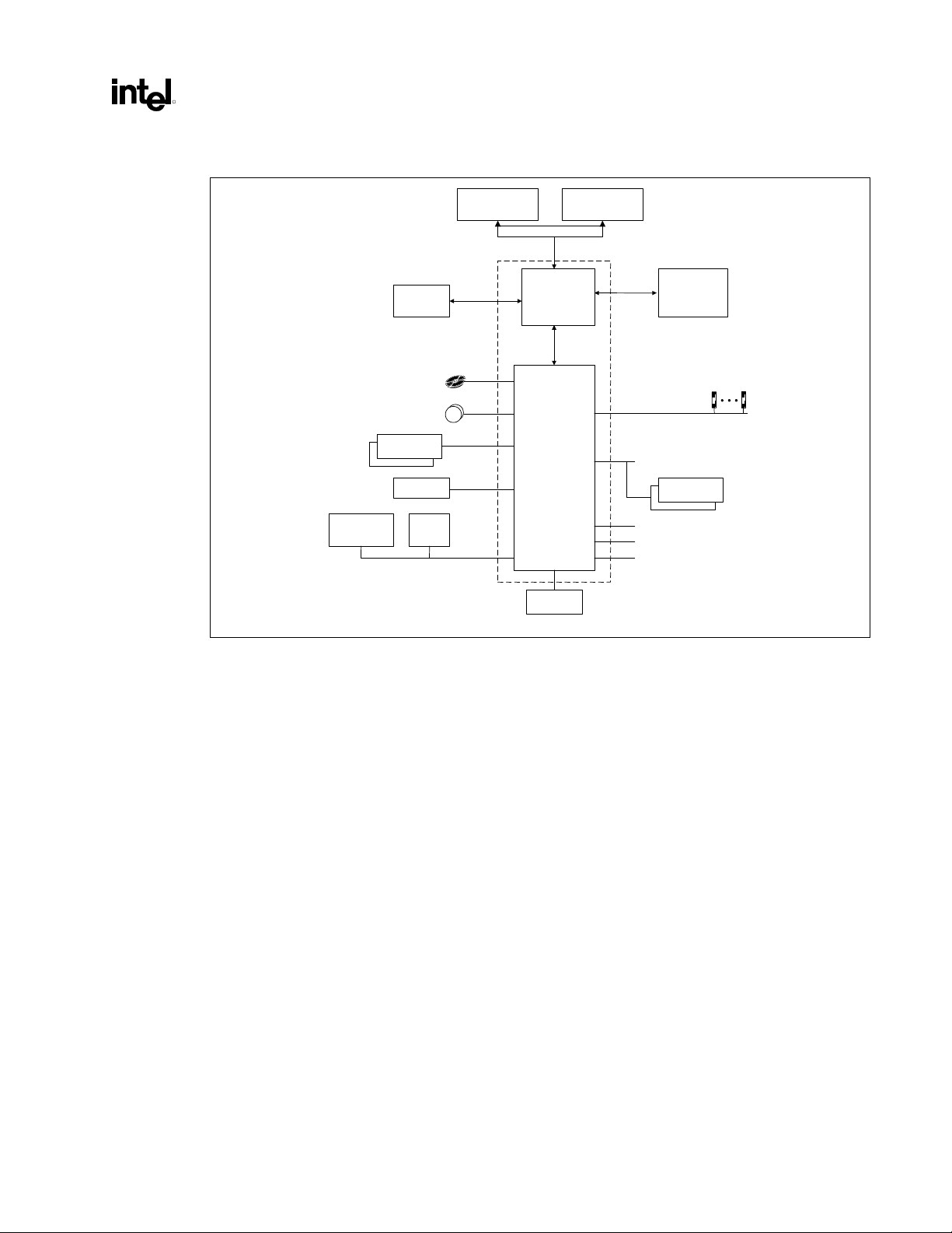
1.3. System Overview
The Intel 820E chipset is designed for Intel
®
Pentium
®
III microprocessors and is the first chipset to
support the integrated LAN capability and expanded USB capability. It supports the 4× capability of the
AGP 2.0 Interface Specification and it supports the 400 MHz Direct RDRAM* interface. The 400 MHz,
16-bit, double-clocked Direct RDRAM interface provides 1.6-GB/s access to main memory. To provide
more efficient communication between chipset components, the hub interface component interconnect is
designed into the Intel 820E chipset.
Support of AGP 4×, 400 MHz Direct RDRAM and the hub interface provides a balanced system
architecture for the Pentium III processor, minimizing bottlenecks and increasing system performance. By
increasing memory bandwidth to 1.6 GB/s by means of 400 MHz Direct RDRAM and by increasing the
graphics bandwidth to 1 GB/s by means of AGP 4×, the Intel 820E chipset delivers the data throughput
necessary to take advantage of the high performance provided by the powerful Pentium III processors.
In addition, the Intel 820E chipset architecture enables security and manageability infrastructures through
the Firmware Hub (FWH)component.
The ACPI-compliant Intel 820E chipset platform can support the Full-On, Stop Grant, Suspend to RAM,
Suspend to Disk, and Soft-Off power management states. Through the use of the integrated LAN
functions, the Intel 820E chipset also supports Wake on LAN* for remote administration and
troubleshooting.
The Intel 820E chipset architecture eliminates the need for the ISA expansion bus traditionally integrated
into the I/O subsystem of Intel chipsets. This eliminates many conflicts experienced when installing
hardware and drivers into legacy ISA systems. The elimination of ISA provides true plug and play for the
Intel 820E chipset platform. Traditionally, the ISA interface was used for audio and modem devices. The
addition of AC’97 allows the OEM to use software-configurable AC’97 audio and modem
encoders/decoders (codecs), instead of traditional ISA devices. The 82801BA ICH2 component expands
the support of AC’97 to include up to 6-channel audio. The ISA bus can be implemented with a PCI-toISA bridge from an external component supplier.
The Intel 820E chipset contains two core components: the Memory Controller Hub (MCH) and the I/O
Controller Hub 2 (ICH2). The MCH integrates the 133 MHz processor system bus controller, an AGP
2.0 controller, a 400 MHz Direct RDRAM controller, and a high-speed hub interface for communication
with the ICH2. The ICH2 integrates an Ultra ATA/100 controller, two USB host controllers, an LPC
interface controller, an FWH Flash BIOS interface controller, a PCI interface controller, an AC’97
digital controller, an integrated LAN controller, and a hub interface for communication with the MCH.
The Intel 820E chipset provides the data buffering and interface arbitration required to ensure that the
system interfaces operate efficiently and provide the system bandwidth necessary to obtain peak
performance with the Pentium III processor.
Design Guide 15
Page 16

Intel® 820E Chipset
R
1.3.1. Chipset Components
The Intel 820E chipset consists of the Intel
®
Intel
82801BA I/O Controller Hub (ICH2). Additional functionality can be provided through the use of
®
82820 Memory Controller Hub (MCH) and the
a PCI-to-ISA bridge.
Memory Controller Hub (MCH)
The MCH provides the interconnect between the Direct RDRAM and the system logic. It integrates the
following functions:
• Support for single or dual Intel PGA370 processors with a 100 MHz or 133 MHz system bus
• 256 MHz, 300 MHz, 356 MHz or 400 MHz Direct RDRAM interface supporting 1 GB of Direct
RDRAM
• 4×, 1.5 V AGP interface (3.3 V 1×, 2×, and 1.5 V 1×, 2× devices also supported)
• Downstream hub interface for access to the ICH2
In addition, the MCH provides arbitration, buffering, and coherency management for each of these
interfaces. Refer to Chapter 2 Layout/Routing Guidelines for more information regarding these
interfaces.
I/O Controller Hub 2 (ICH2)
The ICH2 provides the I/O subsystem with access to the rest of the system. Additionally, it integrates
many I/O functions. The ICH2 integrates:
• Upstream hub interface for access to the MCH
• Two-channel Ultra ATA/100 bus master IDE controller
• Two USB controllers (expanded capabilities for 4 ports)
• I/O APIC
• SMBus controller
• FWH interface (FWH Flash BIOS)
• LPC interface
• AC’97 2.1 interface
• PCI 2.2 interface
• Integrated system management controller
• Alert on LAN*
• Integrated LAN controller
The ICH2 also contains the arbitration and buffering necessary to ensure efficient utilization of these
interfaces. Refer to Section 2 for more information on these interfaces.
16 Design Guide
Page 17
Intel® 820E Chipset
R
FWH Flash BIOS
The FWH Flash BIOS component is a key element in providing a new security and manageability
infrastructure for the PC platform. The device operates under the FWH Flash BIOS interface and
protocol. The hardware features of this device include a unique Random Number Generator (RNG),
register-based locking, and hardware-based locking.
ISA Bridge
For legacy needs, ISA support is an optional feature of the Intel 820E chipset. Implementations that
require ISA support can benefit from the enhancements of the Intel 820E chipset, while “ISA-less”
designs are not burdened with the complexity and cost of the ISA subsystem.
The Intel 820E chipset platform with optional ISA support takes advantage of an external component
supplier’s ISA bridge, which is a PCI-to-ISA bridge that resides on the PCI bus of the ICH2.
1.3.2. Bandwidth Summary
The following table provides a summary of the bandwidth requirements for the Intel 820E chipset.
Table 1. Intel
Processor bus 100/133 1 100/133 8 800/1066
RDRAM 266/300/356/400 2 533/600/711/800 2 1066/1200/1422/1600
AGP 2.0 66 4 266 4 1066
Hub interface 66 4 266 1 266
PCI 2.2 33 1 33 4 133
®
820E Chipset Platform Bandwidth Summary
Interface Clock Speed
(MHz)
Samples
Per Clock
Data Rate
(megasamples/s)
Data Width
(Bytes)
Bandwidth
(MB/s)
Design Guide 17
Page 18

Intel® 820E Chipset
®
R
1.3.3. System Configuration
The following figures show typical platform configurations using the Intel 820E chipset:
Figure 1. Intel
®
820E Chipset Platform Performance Desktop Block Diagram
®
Intel® Pentium
Other ASICs
(optional)
4x AGP
Graphics
Controller
4 IDE Drives
UltraATA/100/66/33
4 USB Ports; 2 HC
AC'97 Codec(s)
(optional)
LAN Connect
Super I/O
AGP 2.0
AC'97 2.1
LPC I/F
III
Processor
Intel® 820E Chipset
Intel® 82820
Controller Hub
(MCH)
Hub
Interface
I/O Controller Hub
Intel® 82801BA
(ICH2)
FWH Flash
BIOS
Main
Memory
(Direct RDRAM*)
PCI Bus
Power Management
Clock Generators
System Management (T CO)
2
SMBus/I
C
GPIO
PCI
Slots
sys_blk_820E
Figure 2. Intel® 820E Chipset Platform Performance Desktop Block Diagram (with ISA Bridge)
®
Intel ® Pentium
Other ASICs
(optional)
4x AGP
Graphics
Controller
4 IDE Drives
UltraATA/100/ 66/33
4 USB Ports; 2 HC
AC'97 Codec(s)
(optional)
LAN Connect
Super I/O
AGP 2.0
AC'97 2.1
LPC I/F
Proc essor
Intel ® 820E Chips et
Intel
82820 Memory
Controller Hub
(MCH)
Hub
Interface
I/O Controller Hub
Intel® 82801BA
(ICH2)
FWH F lash
BIOS
III
Main
Memory
(Direct RDRAM*)
PCI Bus
ISA Bridge
(optional)
Power Management
Clock Generators
System Management (TCO)
SMBus/I 2 C
GPIO
PCI
Slots
ISA
Slots
sys_blk_isa_820E
18 Design Guide
Page 19
Intel® 820E Chipset
R
®
Figure 3. Intel
820E Chipset Platform Dual-Processor Performance Desktop Block Diagram
Other ASICs
(optional)
4x AGP
Graphics
Controller
4 IDE Drives
UltraATA/100/66/33
4 USB Ports; 2 HC
AC'97 Codec(s)
(optional)
LAN Connect
Super I/O
Intel ® Pentium
Processor
AGP 2.0
AC'97 2.1
LPC I/F
®
III
Intel®
22 Mmr
Controller Hub
(MCH)
I/O Controller Hub
Intel® 82801BA
(ICH2)
FWH Flash
BIOS
®
Pentium
Processor
®
Intel
Intel ® 820E Chipset
Hub
Interface
III
Main
Memory
(Direct RDRAM*)
PCI Bus
Power Management
Clock Generators
System Management (T CO)
SMBus/I 2 C
GPIO
PCI
Slots
sys_blk_2P_820E
Design Guide 19
Page 20

Intel® 820E Chipset
R
1.4. Platform Initiatives
1.4.1. Direct Rambus RAM (RDRAM*)
The Direct Rambus RAM (RDRAM) initiative provides the memory bandwidth necessary to obtain
optimal performance from the Pentium III processor as well as a high-performance AGP graphics
controller. The MCH RDRAM interface supports 266 MHz, 300 MHz, 356 MHz, and 400 MHz
operation. The latter delivers 1.6 GB/s of theoretical memory bandwidth, which is twice the memory
bandwidth of 100 MHz SDRAM systems. Coupled with the greater bandwidth, the heavily pipelined
RDRAM protocol provides substantially more efficient data transfer. The RDRAM memory interface can
utilize more than 95% of the 1.6-GB/s theoretical maximum bandwidth.
In addition to the RDRAM’s performance features, the new memory architecture provides enhanced
power management capabilities. The powerdown mode of operation allows Intel 820E chipset-based
systems to provide cost-effective support of Suspend to RAM.
1.4.2. Streaming SIMD Extensions
The Pentium III processor provides 70 new streaming SIMD (single-instruction, multiple-data)
extensions. The Pentium III processor’s new extensions are floating-point SIMD extensions. Intel
MMX™ technology provides integer SIMD extensions. The Pentium III processor’s new extensions
complement the Intel MMX technology SIMD extensions and provide a performance boost to floatingpoint-intensive 3D applications.
1.4.3. AGP 2.0.
In combination with Direct RDRAM memory technology, the AGP 2.0 interface allows graphics
controllers to access main memory at over 1 GB/s, which is twice the AGP bandwidth of previous AGP
platforms. AGP 2.0 provides the infrastructure necessary for photorealistic 3D. In conjunction with
Direct RDRAM and the Pentium III processor’s new streaming SIMD extensions, AGP 2.0 delivers the
next level of 3D graphics performance.
1.4.4. Hub Interface
As the I/O speed has increased, the demand placed on the PCI bus by the I/O bridge has become
significant. With the addition of AC’97 and ATA/100, coupled with the existing USB, I/O requirements
will begin to affect PCI bus performance. The Intel 820E chipset’s hub interface architecture ensures that
the I/O subsystemboth PCI and the integrated I/O features (IDE, AC’97, USB, etc.)will receive
adequate bandwidth. By placing the I/O bridge on the hub interface instead of the PCI, the hub
architecture ensures that both the I/O functions integrated into the ICH2 and the PCI peripherals will
obtain the bandwidth necessary for peak performance. In addition, the hub interface’s lower pin count
allows a smaller package for the MCH and ICH2.
®
20 Design Guide
Page 21

Intel® 820E Chipset
R
1.4.5. Integrated LAN Controller
The ICH2 component incorporates an integrated LAN Controller. Its bus master capabilities enable the
component to process high-level commands and perform multiple operations, which lowers processor
utilization by off-loading communication tasks from the processor.
The ICH2 functions with several options of LAN connect components, allowing the targeting of the
desired market segment. The Intel
The Intel
®
82562ET component provides a basic Ethernet* 10/100 connection. The Intel® 82562EM
®
82562EH component provides a HomePNA 1-Mbit/sec connection.
component provides an Ethernet 10/100 connection with the added flexibility of Alert on LAN. More
advanced LAN solutions can be implemented with the Intel
1.4.6. Ultra ATA/100 Support
The ICH2 (82801BA) component supports the IDE controller with two sets of interface signals (primary
and secondary) that can be enabled independently, tri-stated or driven low. The component supports
UltraATA/100, Ultra ATA/66, UltraATA/33, and multiword p modes for transfers of up to
100 Mbytes/sec.
1.4.7. Expanded USB Support
The ICH2 component contains two USB host controllers. Each host controller includes a root hub with
two separate USB ports each, for a total of four USB ports. The addition of a USB host controller
expands the functionality of the platform.
1.4.8. Manageability
The Intel 820E chipset platform integrates several functions designed to manage the system and lower
the system’s total cost of ownership (TCO). These system management functions are designed to report
errors, diagnose the system, and recover from system lock-ups, without the aid of an external
microcontroller.
®
82550 or other PCI-based product offerings.
TCO Timer
The ICH2 integrates a programmable TCO timer, which is used to detect system locks. The first
expiration of the timer generates an SMI#, which the system can use to recover from a software lock. The
second expiration of the timer causes a system reset, to recover from a hardware lock.
Processor Present Indicator
The ICH2 looks for the processor to fetch the first instruction after reset. If the processor does not fetch
the first instruction, the ICH2 will reboot the system at the safe-mode frequency multiplier.
ECC Error Reporting
After detecting an ECC error, the MCH can send one of several messages to the ICH2. The MCH can
instruct the ICH2 to generate either an SMI#, NMI#, SERR# or TCO interrupt.
Design Guide 21
Page 22

Intel® 820E Chipset
R
Function Disable
The ICH2 provides the ability to disable the following functions: AC’97 Modem, AC’97 Audio, IDE,
USB or SMBus. Once disabled, these functions no longer decode I/O, memory or PCI configuration
space. Also, no interrupts or power management events are generated by the disabled functions.
Intruder Detect
The ICH2 provides an input signal (INTRUDER#) that can be attached to a switch that is activated when
the system case is opened. The ICH2 can be programmed to generate an SMI# or TCO interrupt resulting
from an active INTRUDER# signal.
SMBus
The ICH2 integrates an SMBus controller. The SMBus provides an interface to manage peripherals such
as serial presence detection (SPD) on RIMMs and thermal sensors. The slave interface allows an external
microcontroller to access system resources.
The Intel 820E chipset platform integrates several functions designed to expand the capability of
interfacing several components to the system.
Interrupt Controller
The interrupt capabilities of the Intel 820E chipset platform expands support for up to eight PCI interrupt
pins and PCI 2.2 message-based interrupts. In addition, the ICH2 supports system bus interrupt delivery.
FWH Flash BIOS
The Intel 820E chipset-based system platform supports firmware hub BIOS memory sizes up to 8 MB,
for increased system flexibility.
Alert on LAN*
The ICH2 supports Alert on LAN. In response to a TCO event (intruder detect, thermal event, processor
not booting), the ICH2 sends a message over ALERTCLK and ALERTDATA to alert the network
manager.
22 Design Guide
Page 23

Intel® 820E Chipset
R
1.4.9. AC’97
The Audio Codec ’97 (AC’97) specification defines a digital interface that can be used to attach an audio
codec (AC), a modem codec (MC), an audio/modem codec (AMC) or both an AC and an MC. The
AC’97 specification defines the interface between the system logic and the audio or modem codec,
known as the AC’97 Digital Link.
The Intel 820E chipset platform’s AC’97 (with the appropriate codecs) not only replaces ISA audio and
modem functionality, but also improves overall platform integration by incorporating the AC’97 digital
link. The use of the ICH2-integrated AC’97 digital link reduces cost and eases migration from ISA.
By using an audio codec, the AC’97 digital link allows for cost-effective, high-quality, integrated audio
on an Intel 820E chipset-based platform. In addition, an AC’97 soft modem can be implemented with the
use of a modem codec. Several system options exist when implementing AC’97. The ICH2-integrated
digital link allows several external codecs to be connected to the ICH2. The system designer can provide
audio with an audio codec, a modem with a modem codec, or an integrated audio/modem codec (Figure
4C). The digital link is expanded to support two audio codecs or a combination of an audio and modem
codec (Figures 4A and 4B).
The modem implementations for different countries must be taken into consideration, because telephone
systems may vary. By using a split design, the audio codec can be on-board and the modem codec can be
placed on a riser. Intel is developing an AC’97 digital link connector. With a single integrated codec, or
AMC, both audio and modem can be routed to a connector near the rear panel, where the external ports
can be located.
The digital link in the ICH2 is compliant with Revision 2.1 of the AC’97 specification, so it supports two
codecs with independent PCI functions for audio and modem. Microphone input and left and right audio
channels are supported for a high quality, two-speaker audio solution. Wake on Ring from Suspend also
is supported with the appropriate modem codec.
The ICH2 expands the audio capability with support for up to six channels of PCM audio output (full
AC3 decode). Six-channel audio consists of Front Left, Front Right, Back Left, Back Right, Center, and
Woofer, for a complete surround-sound effect. ICH2 has expanded support for two audio codecs on the
AC’97 digital link.
Design Guide 23
Page 24

Intel® 820E Chipset
R
Figure 4. (A-C) AC’97 Connections
4A. AC'97 with Audio Codecs (4-Channel Secondary)
AC’97
Audio
Codec
Audio Port
AC’97
Audio
Codec
Audio Port
ICH2 360
EBGA
AC’97 Digital
Link
4B. AC'97 with Modem and Audio Codecs
AC’97 Digital
ICH2 360
EBGA
4C. AC'97 with Audio/Modem Codec
ICH2 360
EBGA
Link
AC’97 Digital
Link
Modem Port
AC’97
Modem
Codec
AC’97
Audio/
Codec
Audio Port
Modem Port
AC’97
Audio/
Modem
Codec
Audio Port
AC97_conn
24 Design Guide
Page 25

Intel® 820E Chipset
R
1.4.10. Low-Pin-Count (LPC) Interface
In the Intel 820E chipset platform, the super I/O component has migrated to the Low-Pin-Count (LPC)
interface. Migration to the LPC interface enables lower-cost super I/O designs. The LPC super I/O
component requires the same feature set as traditional super I/O components. It should include a
keyboard and mouse controller, floppy disk controller, and serial and parallel ports. In addition to the
super I/O features, an integrated game port is recommended because the AC’97 interface does not
provide support for a game port. In systems with ISA audio, the game port typically existed on the audio
card. The fifteen-pin game port connector provides for two joysticks and a two-wire MPU-401 MIDI
interface. Consult your super I/O vendor for a comprehensive list of devices offered and features
supported.
In addition, depending on system requirements, a device bay controller and USB hub could be integrated
into the LPC super I/O component. For systems requiring ISA support, an ISA-IRQ to serial-IRQ
converter is required. This converter could be integrated into the super I/O.
Design Guide 25
Page 26

Intel® 820E Chipset
R
This page is intentionally left blank.
26 Design Guide
Page 27

Intel® 820E Chipset
R
2. Layout/Routing Guidelines
This chapter documents the motherboard layout and routing guidelines for Intel 820E chipset-based
systems. This chapter does not discuss the functional aspects of any bus or the layout guidelines for an
add-in device.
Caution: If the guidelines in this document are not followed, it is very important to complete thorough signal
integrity and timing simulations for each design. Even if the guidelines are followed, critical signals still
should be simulated to ensure proper signal integrity and flight time. As bus speeds increase, it is
imperative that the guidelines documented be followed precisely. Any deviation from these guidelines
must be simulated!
2.1. General Recommendations
The trace impedance typically noted (i.e., 60 Ω ± 10%) is the “nominal” trace impedance. That is, it is
the impedance of a trace when not subjected to the fields created by changing the current in neighboring
traces. When calculating flight times, it is important to consider the minimum and maximum impedance
of a trace based on the switching of neighboring traces. This trace-to-trace coupling can be minimized by
using wider spaces between the traces. In addition, these wider spaces reduce crosstalk and settling time.
Coupling between two traces is a function of the coupled length, the distance separating the traces, the
signal edge rate, and the degree of mutual capacitance and inductance. To minimize the effects of traceto-trace coupling, the routing guidelines documented in this chapter should be followed. In addition, the
PCB should be fabricated as documented in Section 5.1.
Except where noted, all recommendations in this chapter assume 5 mil-wide traces. If the trace width is
greater than 5 mils, then the trace spacing requirements must be adjusted accordingly (and linearly). For
example, this chapter recommends routing most AGP signals with 5 mil traces on 20 mil spaces (1:4). If
6 mil traces are used, then 24 mil spaces must be used (also 1:4). Using a wider trace—and therefore
wider spaces—will make routing more difficult.
Additionally, these routing guidelines are created using the stack-up described in Section 5.1. If this
stack-up is not used, extremely thorough simulations of every interface must be completed. Using a
thicker dielectric (prepreg) will make routing very difficult or impossible.
2.2. Component Quadrant Layout
The quadrant layouts shown are approximate and the exact ball assignments should be used to conduct
routing analysis. These quadrant layouts are designed for use during component placement.
Design Guide 27
Page 28

Intel® 820E Chipset
y
R
Figure 5. MCH 324-Ball µBGA* CSP Quadrant Layout (Top View)
Pin 1
System bus
GP 2.0
(324-Ball
µBGA* CSP)
Hub interface
Direct RDRAM*
Figure 6. ICH2 360-Ball EBGA Quadrant Layout (Top View)
Hub interface
LAN
Processor
ICH2
360-Ball
EBGA
MCH
stem bus
S
mch_quad
IDE
SM bus
AC'97
PCI LPC USB
quad_ICH2
28 Design Guide
Page 29

Intel® 820E Chipset
R
2.3. Intel® 820E Chipset Component Placement
Notes:
1. The ATX and NLX placements and layouts shown in the following figure are recommended for
single (UP) Intel 820E chipset-based system design.
2. The trace length limitation between critical connections will be discussed later in this document.
3. The figure is for reference only.
Figure 7. Sample ATX and NLX MCH/ICH2 Component Placement
a. Sample ATX MCH/ICH2 Component Placement
CPU Host
Bus
ICH2
b. Sample NLX MCH/ICH2 Component Placement
RDRAM* Termination
Direct RDRAM
MCH
CPU Host Bus
AGP
2.0
Hub
Interface
RDRAM Termination
Direct
RDRAM
MCH
atx_mch-ich2 _place
AGP 2.0
Hub Link
ICH2
nlx_mch-ich2 _place
Note: Actual ICH2 placement may vary.
Design Guide 29
Page 30
Intel® 820E Chipset
R
2.4. Core Chipset Routing Recommendations
The following two figures show MCH core routing examples:
Figure 8. Primary-Side MCH Core Routing Ex ample (ATX)
30 Design Guide
Page 31

Intel® 820E Chipset
R
Figure 9. Secondary-Side MCH Core Routing Example (ATX)
Design Guide 31
Page 32

Intel® 820E Chipset
R
2.5. Source-Synchronous Strobing
A technology used in AGP 4×, Direct RDRAM and the hub interface, source-synchronous strobing
allows very high data transfer rates. As buses become faster and cycle times become shorter, the
propagation delay becomes a limiting factor in the bus speed. Source-synchronous strobing is used to
minimize the effect of propagation delay (T
A source-synchronous-strobed interface uses strobe signals, instead of the clock, to indicate that data is
valid. Refer to the following example figure:
Figure 10. Data Strobing Example
Clock
Strobe
) on maximum bus frequency.
PROP
Data
Sample
Data
For a source-synchronous-strobed interface, it is very important that the strobe signals be routed
carefully. These signals must be very clean (i.e., free of noise). Data signals typically are latched on the
rising or falling edge of the strobe signal (or both). If there is noise on these signals, it could cause an
extra “edge” to be detected, thus latching incorrect data. Refer to the following example figures.
Figure 11. Effect of Crosstalk on Strobe Signal
a) Correct Strobing Example (no noise) b) Effect of Cro ss Talk on Strobe Signal
Data correctly
Clock
data
Threshold
Strobe
latched as 0
Clock
data
Threshold
Strobe
Data incorrectly
latched as 1
Noise
(i.e.,
crosst alk)
data_str
strobing_example
Some buses have more than one strobe (i.e., AGP). The AGP 1.0 specification (1× and 2× modes)
employs three strobe signals, each of which is used to strobe different data signals (i.e., each strobe has
an associated set of data signals). The associations for AGP 1.0 (AGP 2×) are listed in the following
table. Refer to Section 2.8 for more information on AGP 2.0 (AGP 4×, 1.5 V).
32 Design Guide
Page 33

Intel® 820E Chipset
R
Table 2. AGP 2× Data/Strobe Association
Data Associated Strobe
AD[15:0] and C/BE[1:0]# AD_STB0
AD[31:16] and C/BE[3:2]# AD_STB1
SBA[7:0] SB_STB
In this example, the lower address signals (AD[15:0]) are sampled on the rising and falling edges of
AD_STB0, while the upper address signals (AD[31:16]) are sampled on the rising and falling edges of
AD_STB1.
When routing strobes and their associated data lines, trace length mismatch is very important, in addition
to noise immunity. The primary benefit of source-synchronous strobing is that the data and the strobe
arrive simultaneously at the receiver. Thus, a strobe and its associated data signals have very critical
length mismatch requirements. With well matched trace lengths (as well as matched impedance), the
propagation delays for the strobe and the data will be very close. Hence, the strobe and the data arrive
simultaneously at the receiver. For some interfaces, the trace length mismatch requirement is less than
0.25 inch.
2.6. Differential Clocking/Strobing
AGP 2× timings are referenced at a particular level on the rising or falling strobe edge, while 4× timings
are referenced to the crossover point of the differential strobes. The crossover is targeted to be at
0.5 V
DDQ
.
2.7. Direct RDRAM* Interface
The Direct RDRAM channel is a multi-symbol interconnect. Because of the length of the interconnect
and the frequency of operation, this bus is designed to allow multiple command and data packets to be
present on a signal wire at any given instant. The driving device sends the next data out before the
previous data has left the bus.
Figure 12. RIMM Diagram
The nature of the multi-symbol interconnect forces many requirements on the bus design and topology.
First and foremost, a drastic reduction in reflected voltage levels is required. The interconnect
transmission lines must be terminated at their characteristic impedance, or the reflected voltage resulting
from an impedance mismatch will degrade the signal quality. These reflections will reduce noise and
timing margins and will reduce the maximum operating frequency of the bus. The reflections could
create data errors.
Design Guide 33
Page 34

Intel® 820E Chipset
R
Because of the tolerances of components such as PCBs, connectors, and termination resistors, there will
be some reflected voltage on the interconnect. In this multi-symbol interconnect, timings are pattern
dependent because the reflections interfere with the next transfer.
Additionally, coupled noise can greatly affect the performance of high-speed interfaces. Just as in sourcesynchronous designs, the odd- and even-mode propagation velocity change creates a skew between the
clock and data or command lines, which reduces the maximum operating frequency of the bus. Efforts
must be made to significantly decrease the crosstalk, as well as the other sources of skew.
To achieve these bus requirements, the Direct RDRAM channel is designed to operate as a transmission
line. All components, including the individual RDRAMs, are incorporated into the design to create a
uniform bus structure that can support up to 33 devices (including the MCH), running at
800 megatransfers/second (MT/s).
2.7.1. Stack-Up
The perfect matching of transmission line impedance and a uniform trace length is essential for the Direct
RDRAM interface to work properly. Maintaining a 28 Ω (± 10%) loaded impedance for every RSL
(Direct RDRAM Signaling Level) signal has changed the requirements for trace width and prepreg
thickness for the Intel 820E chipset platform. (Refer to Section 5.1.)
Achieving a 28 Ω nominal impedance with a traditional 7 mil prepreg requires 28 mil-wide traces. These
traces are too wide to break out of the two rows of RSL balls on the MCH. To reduce the trace width, a
4.5 mil-thick prepreg is required. This thinner prepreg allows 18 mil-wide traces to meet the 28 Ω
(± 10%) nominal impedance requirement. (Refer to Section 5.1, for detailed stack-up requirements.)
2.7.2. Direct RDRAM* Layout Guidelines
The signals on the Direct RDRAM channel are broken into three groups: RSL signals, CMOS signals,
and clocking signals as follows:
• RSL signals
DQA[8:0]
DQB[8:0]
RQ[7:0]
• CMOS signals
CMD (high-speed CMOS signal)
SCK (high-speed CMOS signal)
SIO
• Clocking signals
CTM, CTM#
CFM, CFM#
34 Design Guide
Page 35
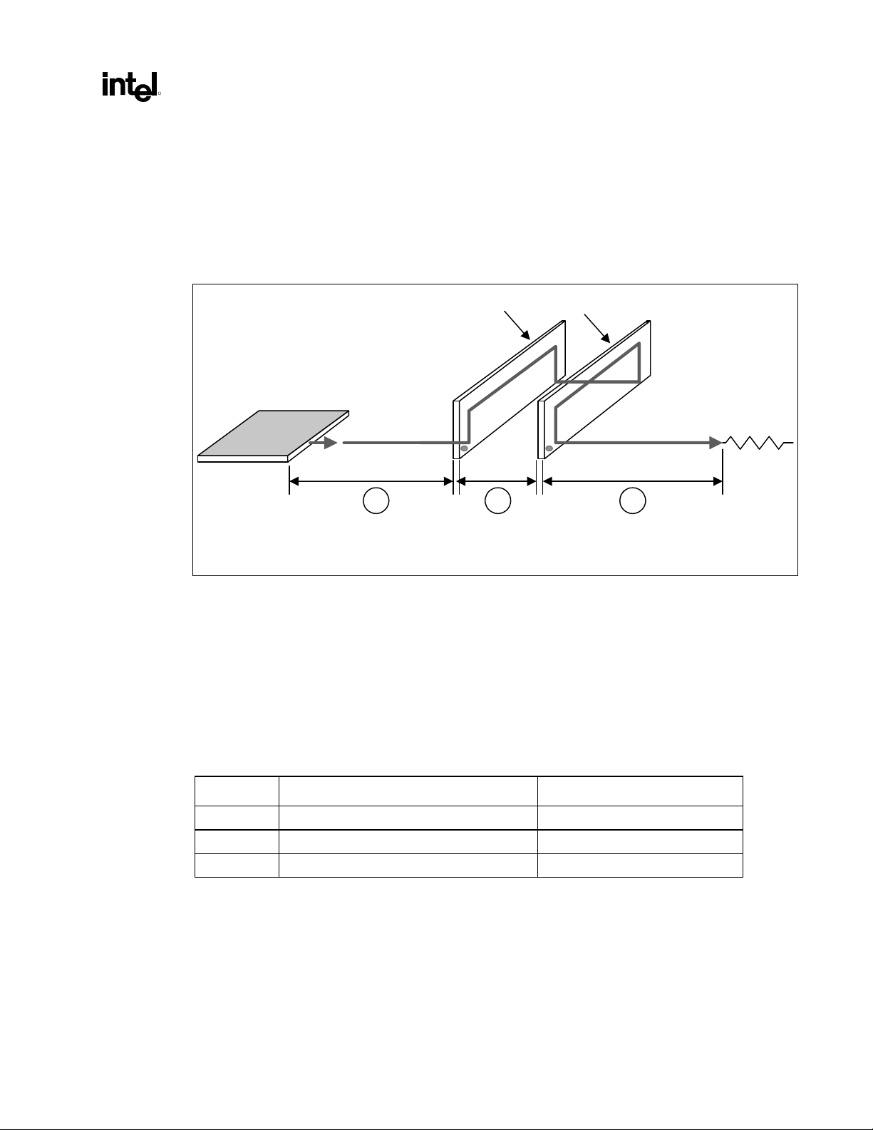
Intel® 820E Chipset
R
2.7.2.1. RSL Routing
The RSL signals enter the first RIMM on the left side, propagate through the RIMM, and exit on the
right. The signal continues through the rest of the existing RIMMs until it is terminated at V
unpopulated slots must have continuity modules in place to ensure that the signals propagate to the
termination.
Figure 13. RSL Routing Dimensions
RIMM_0 RIMM_1
MCH
TERM
. All
0"-3.50"
0.4"-0.45"
A B C
MCH to first
RIMM
RIMM to
RIMM
To maintain a nominal 28 Ω trace impedance, the RSL signals must be 18 mils wide. To control crosstalk
and odd/even-mode velocity deltas, there must be a 10 mil ground isolation trace routed between
adjacent RSL signals. The 10 mil ground isolation traces must be connected to ground with a via every 1
inch. A 6 mil gap is required between the RSL signals and the ground isolation trace. These signals must
be length-matched to ±10 mils in line section A and to ±2 mils in line section B, using the trace length
matching methods in Section 2.7.2.6. To ensure uniform trace lines, trace width variation must be
uniform on all RSL signals at every neckdown for each line section. All RSL signals must have the same
number of vias. It may be necessary to place vias on RSL signals where they are not necessary to meet
this via loading requirement (i.e., dummy vias).
Table 3. Placement Guidelines for Motherboard Routing Lengths
Reference Trace Description Maximum Trace Length (in.)
A MCH to first RIMM connector 0 to 3.50
B RIMM to RIMM 0.4 to 0.45
C RIMM to termination 0 to 3
0"-3"
RIMM to
Termination
rsl_route
Design Guide 35
Page 36

Intel® 820E Chipset
R
The following figure shows a top view of the trace width/spacing requirements for the RSL signals.
Figure 14. RSL Routing Diagram
18 mils
6 mils
10 mils
6 mils
18 mils
6 mils
10 mils
6 mils
Space
Space
Space
Space
The following two figures show the top view of an example RSL breakout and route.
Figure 15. Primary-Side RSL Breakout Example
RSL Signal Trace
Ground
RSL Signal Trace
Ground
rsl_route_dia
36 Design Guide
Page 37

Intel® 820E Chipset
R
Figure 16. Secondary-Side RSL Breakout Example
Design Guide 37
Page 38

Intel® 820E Chipset
R
2.7.2.2. RSL Termination
All RSL signals must be terminated to 1.8 V (V
the channel opposite the MCH. Resistor packs are acceptable. V
speed bypass capacitors—one 0.1 µF ceramic chip capacitor per two RSL lines—near the terminating
resistors. Additionally, bulk capacitance is required. Assuming a linear regulator with an approximately
20 ms response time, two 100 µF tantalum capacitors are recommended. The trace length between the
last RIMM and the termination resistors should be less than 3 inches. Length matching in this section of
the channel is not required. The V
not be supplied during Suspend to RAM.
Figure 17. Direct RDRAM Termination
RSL Signals
) using 27-Ω 1% or 28 Ω 2% resistors at the end of
TERM
must be decoupled using high-
TERM
power island should be at least 50 mils wide. This voltage need
TERM
Terminator
R-packs
V
TER M
direct_rdram_term
Note: It is necessary to compensate for the slight difference in electrical characteristics between a dummy via
and a real via. Refer to Section 2.7.2.7 for more information on via compensation.
38 Design Guide
Page 39

Intel® 820E Chipset
R
Figure 18. Direct RDRAM* Termination Example
2.7.2.3. Direct RDRAM* Ground Plane Reference
All RSL signals must be referenced to GND to provide the optimal current return path. The Direct
RDRAM ground plane reference must be continuous to the V
island under the RSL signals must be continuous from the last RIMM to the back of the termination
capacitors. Choose a reference island shape that does not compromise power delivery to the components.
The return current will flow through the V
capacitors into the ground island and under the RSL
TERM
traces. Any split in the ground island will provide a suboptimal return path. In a four-layer board, this
will require the V
island to be on an outer layer. The V
TERM
top layer.
Design Guide 39
capacitors. The ground reference
TERM
island should always be placed on the
TERM
Page 40

Intel® 820E Chipset
R
Figure 19. Incorrect Direct RDRAM* Ground Plane Referencing
MCH
Wrong
1.8-V Plane
RIMM1
RIMM2
Figure 20. Direct RDRAM* Ground Plane Reference
MCH
GND Plane
1.8-V Plane
Required
3.3-V Plane
dir_Rambus_gnd_plane_ref_incorrect
3.3-V Plane
RIMM1
GND PlaneGND Plane
RIMM2
V
TERM
resistors
TERM
capacitors
Extend GND plane
reference island beyond
TERM
capacitors
V
Vterm layer not shown
The ground reference island under the RSL signals MUST be connected to the ground pins on the RIMM
connector and the ground vias used to connect the ground isolation on the first and fourth layers.
40 Design Guide
V
dir_Rambus_gnd_plane_ref
Page 41

Intel® 820E Chipset
R
All four layers of the motherboard require correct grounding between the RSL signals on the
motherboard, as follows:
• Layer 1 = Ground isolation
• Layer 2 = Ground plane
• Layer 3 = Ground reference in the power plane
• Layer 4 = Ground isolation
All ground vias and pins MUST be connected to all 4 layers.
2.7.2.4. Direct RDRAM* Connector Compensation
The RIMM connector inductance causes an impedance discontinuity on the Direct RDRAM channel.
This may reduce the voltage and timing margin.
To compensate for the inductance of the connector, an approximately 0.65 pF to 0.85 pF compensating
capacitive tab (C-TAB) is required on each RSL connector pin. This compensating capacitance must be
added to the following connector pins at each connector:
LCTM LCTM#
RCTM RCTM#
LCFM LCFM#
RCFM RCFM#
LROW[2:0] RROW[2:0]
LCOL[4:0] RCOL[4:0]
RDQA[8:0] LDQA[8:0]
RDQB[8:0] LDQB[8:0]
SCK CMD
This can be achieved on the motherboard by adding a copper tab to the specified RSL pins at each
connector. The target value is approximately 0.65 pF – 0.85 pF. The copper tab area for the
recommended stack-up was determined by means of simulation. The copper tabs can be placed on any
signal layer, independently of the layer on which the RSL signal is routed.
The following equation is an approximation usable for calculating the copper tab area on an outer layer.
Equation 1. Approximate Copper Tab Area Calculation
Length × Width = Area = C
Where:
= 2.25 × 10
ε
0
= Relative dielectric constant of prepreg material
ε
r
-16
× Thickness of prepreg / [(ε0) (ε
PLATE
Farads/mil
) (1.1)]
r
Thickness of prepreg (stack-up dependent)
Length, Width = Dimensions (in mils) of copper plate to be added
Factor of 1.1 accounts for fringe capacitance.
Based on the stack-up requirement in Section 5.1, the copper tab area should be 2800 to 3600 square
mils. Different stack-ups require different copper tab areas. The following table lists example copper tab
areas.
Design Guide 41
Page 42

Intel® 820E Chipset
R
Table 4. Copper Tab Area Calculation
Dielectric
Thickness
(D)
4.5 6 10 6 0.65 2800 140 L x 20 W
Separation between
Signal Trace and
Copper Tab
Min.
Ground
Flood
Air Gap
between Signal
and GND Flood
Based on Equation 1, the tab area is 2800 sq. mils, where ε
Compensating
Capacitance
(pF)
is 4.2 and D is 4.5. These values are based
r
Copper Tab
(C-TAB) Area
(A) (sq. mils)
C-TAB
Shape
(mils)
70 L x 40 W
on 2116 prepreg material.
Note that more than one copper tab shape may be used. The tab dimensions are based on the copper area
over the ground plane. The actual length and width of the tabs may differ as a result of routing
constraints (e.g., if the tab must extend to center of hole, or antipad). However, each copper tab should
have the equivalent area. For example, the copper tabs in Figure 21 have the following dimensions, when
measured tangentially to the antipad:
Inner C-TAB = 140 (length) × 20 (width)
Outer C-TAB = 70 (length) × 40 (width)
Figures 21 through 25 show a routing example of tab compensation capacitors. Note that ground floods
around the RIMM pins must not be interrupted by the capacitor tabs, and they must be connected to
avoid discontinuity in the ground plane, as shown.
42 Design Guide
Page 43

Intel® 820E Chipset
R
Figure 21. Connector Compensation Example
Design Guide 43
Page 44

Intel® 820E Chipset
R
Figure 22. Section A (See Note), Top Layer
Note: Refer to Figure 21. For clarity, the ground flood was removed from the picture.
44 Design Guide
Page 45
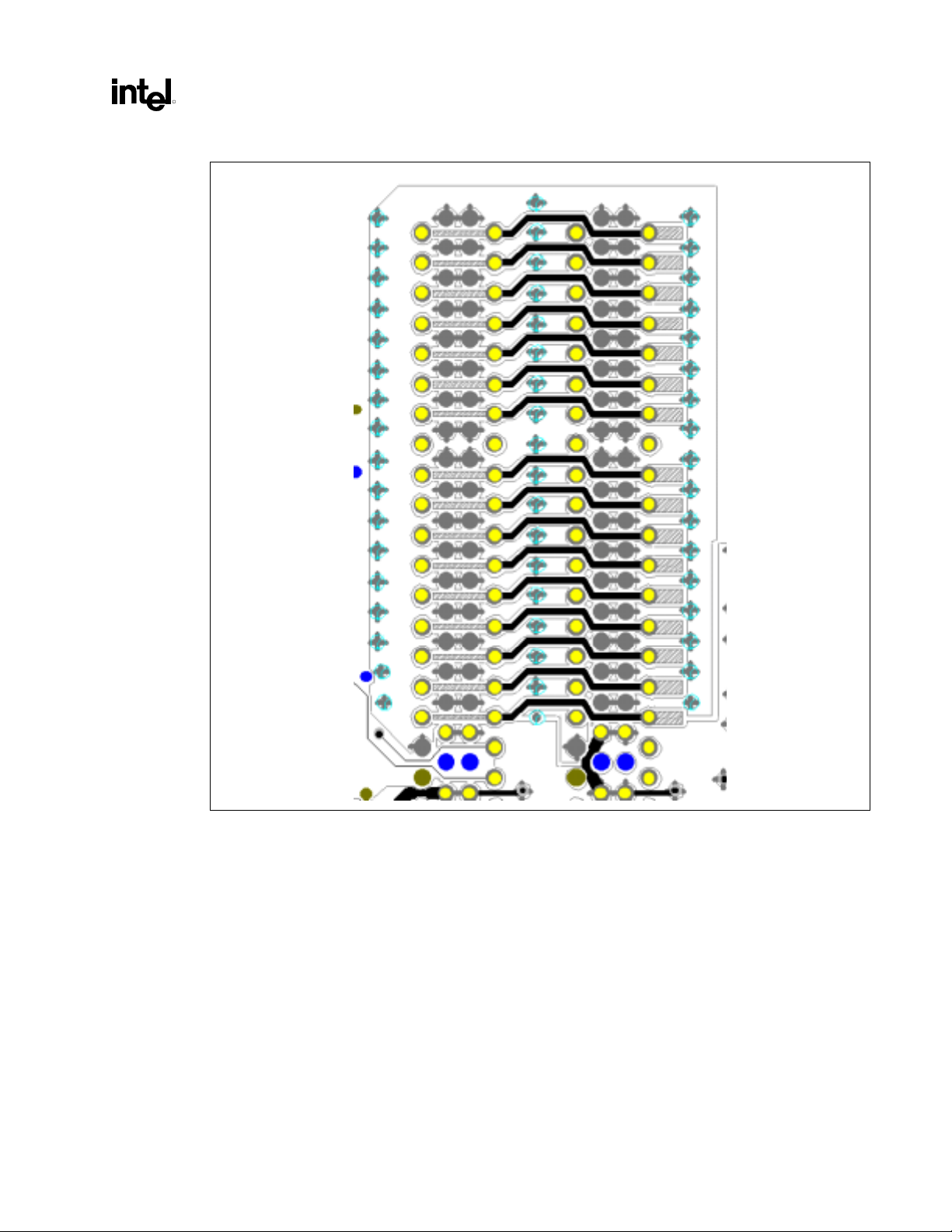
Intel® 820E Chipset
R
Figure 23. Section A (See Note), Bottom Layer
Note: Refer to Figure 21. For clarity, the ground flood was removed from the picture.
Design Guide 45
Page 46

Intel® 820E Chipset
R
Figure 24. Section B (See Note), Top Layer
Note: Refer to Figure 21. For clarity, the ground flood was removed from the picture.
46 Design Guide
Page 47

Intel® 820E Chipset
R
Figure 25. Section B (See Note), Bottom Layer
Note: Refer to Figure 21. For clarity, the ground flood was removed from the picture.
2.7.2.4.1. Di r ect RDRAM* Channel Connector Compensation Enhancement
Recommendation
From further analysis, it was determined that the amount of capacitance needed for RSL traces depends
on the lengths that the signals have to travel though the RIMM connector pin. (i.e., a signal on the bottom
layer has to travel through more of the RIMM connector pin than a signal on the top layer). As a result of
the travel through the pin, signals routed on the bottom layer have a larger inductance at the connector,
which causes a larger impedance discontinuity, resulting in a possible reduction of voltage and timing
margin on those signals. As a result, RSL traces on the bottom layer need more capacitive compensation
than RSL traces routed on the top layer. RSL signals routed on the bottom layer need 0.55 pF more
compensation than signals routed on the top layer. To compensate for the inductance of the connector,
approximately 0.65 pF to 0.85 pF compensating capacitive tabs (C-TAB) are required for each topside
RSL trace, and approximately 1.20 pF – 1.4 pF is required for each bottom-side RSL trace.
Table 5. RSL and Clocking Signal RIMM Connector Capacitance Recommendations
RSL and Clocking Signal Routing Layer Capacitance (pF)
Top 0.65 – 0.85
Bottom 1.20 – 1.40
Design Guide 47
Page 48

Intel® 820E Chipset
R
The copper tab area for the recommended stack-up was determined by means of simulation. The amount
of capacitance required is determined by the layer on which the RSL or clocking signal is routed. The
copper tabs can be placed on any signal layer, independently of the layer on which the RSL signal is
routed.
The following example calculation uses Equation 1. Approximate Copper Tab Area Calculation for a
board with an ε
of 4.2 and a prepreg thickness of 4.5 mils. Note that these numbers vary with the
r
difference in prepreg thickness.
Table 6. Copper Tab Area Calculation
Layer Dielectric
Thickness
Top 4.5 6 10 6 0.65 – 0.85 ~2810 – 3680
Bottom 4.5 6 10 6 1.20 – 1.40 ~5194 – 6060
Separation
Between
Signal Traces
& Copper Tab
Min.
Ground
Flood
Air Gap
between
Signal &
GND Flood
Compensating
Capacitance in
Note that more than one copper tab shape may be used, as shown in Figure 26. The dimensions are based
on the copper area over the ground plane. The actual length and width of the tabs may differ due to
routing constraints (e.g., if tab must extend to center of hole or anti-pad). Figures 26 through 28 show a
tab compensation capacitor routing example. Note that the capacitor tabs must not interrupt ground
floods around the RIMM pins, and they must be connected, to avoid discontinuity in the ground plane, as
shown.
Figure 26. Top-Layer CTAB with RSL Signal Routed on the Same Layer (C
Cplate (pF)
= 0.8 pF)
EFF
CTAB Area
(sq. mils)
Figure 27. Bottom-Layer CTAB with RSL Signal Routed on the Same Layer (C
= 1.35 pF)
EFF
48 Design Guide
Page 49

Intel® 820E Chipset
R
The CTAB can be implemented on the multiple layers to minimize routing and space constraints. Figure
28 shows the use of CTABs on the top and bottom layer for bottom-layer RSL and clocking signals
routed between RIMMs.
Figure 28. Bottom-Layer CTABs Split across the Top and Bottom Layer to Achieve an Effect
C
~1.35 pF
EFF
2.7.2.5. RSL Signal Layer Alternation
RSL signals must alternate layers as they are routed through the channel. If a signal is routed on the
primary layer from the MCH to the first RIMM socket, it must be routed on the secondary layer from the
first RIMM to the second RIMM, as shown in Figure 29 (signal B). If a signal is routed on the secondary
layer from the MCH to the first RIMM socket, it must be routed on the primary side from the first RIMM
to the second RIMM, as shown in Figure 29 (signal A). Signals can be routed on either layer from the
last RIMM to the termination resistors.
Design Guide 49
Page 50

Intel® 820E Chipset
R
Figure 29. RSL Signal Layer Alternation
Signal B
Signal on secondary side
Signal on primary side
Signal A
Signal A
MCH
Signal B
Route on EITHER layer.
Ground isolation is
REQUIRED!
Term
Table 7. RSL Routing Layer Requirements
MCH to 1st RIMM 1st RIMM to 2nd RIMM
Method 1 Primary side Secondary side
Method 2 Secondary side Primary side
2.7.2.6. Length Matching Methods
To allow for greater routing flexibility, the RSL signals require pad-to-pin length matching between the
MCH and the first connector. If the trace lengths are matched between the balls of the MCH and the pin
of the RIMM connector, the length mismatch between the pad (on the die) and the ball has not been
taken into account. However, given the package dimension, which represents the length from the pad to
the ball, the routing can compensate for this package mismatch. Therefore, the board length mismatch
can be increased.
The RSL channel requires the matching of the trace lengths from pad to pin within ±10 mils.
Given the following definitions:
• Package dimension: Representation of length from pad to ball
• Board trace length: Trace length on board
rsl_sig-lay_ alter.vsd
• Nominal RSL length: Length to which all signals are matched. (Note: There is not necessarily a
trace that is exactly to nominal length, but all RSL signals must be matched to within ±10 mils of
the nominal length.) The nominal RSL length is an arbitrary length, within the limits of the routing
guidelines, to which all the RSL signals will be matched (within 10 mils).
50 Design Guide
Page 51

Intel® 820E Chipset
R
All RSL signals must satisfy the following equation:
Equation 2. RDRAM RSL Signal Trace Length Calculation
Package dimension + board trace length = Nominal RSL length ± 10 mils
Figure 30. Example of RDRAM Trace Length Matching
L1, L2: Package dimensions
L3, L4: Board trace length
L1
MCH Package
MCH
MCH
Die
Die
L2
L1 + L3 = Nominal RSL length ±10 mils
L2 + L4 = Nominal RSL length ±10 mils
Ball
L3
L4
R
I
M
M
C
o
n
n
e
c
t
o
r
R
I
M
M
C
o
n
n
e
c
t
o
r
rdram_tr_l en.vsd
Note: Refer to the Intel® 820 Chipset Family: 82820 Memory Controller Hub (MCH) Datasheet for the
component package dimensions.
The RDRAM clocks (CTM, CTM#, CFM, and CFM#) must be longer than the RDRAM signals, due to
their increased trace velocity (because they are routed as a differential pair). To calculate the length for
each clock, the following formula should be used:
V
t
e
r
m
Equation 3. RDRAM Clock Signal Trace Length Calculation
Clock length = Nominal RSL signal length (package + board) × 1.021
This formula yields clock signals 21 mils/inch longer than the nominal length. The lengthening of the
clock signals to compensate for their trace velocity change only applies to routing between the MCH and
the first RIMM. The clock signal lengths should be matched to the RSL signals between RIMMs. For
more detailed clock routing guidelines, refer to Chapter 4 Clocking.
The high-speed CMOS signals must be length-matched to the RSL signals within 1200 mils (1.2 inches),
as the result of a timing requirement between the CMOS and RSL signals during NAP Exit and PDN
Exit.
Design Guide 51
Page 52

Intel® 820E Chipset
R
It is necessary to compensate for the slight difference in electrical characteristics between a dummy via
and a real via. Refer to the following section for more information on via compensation.
2.7.2.7. Via Compensation
As described in Section 2.7.2.1, all signals must have the same number of vias. As a result, each trace
will have one via (near the BGA pad) because some RSL signals must be routed on the bottom of the
motherboard. Therefore, it is necessary to place a dummy via on all signals that are routed on the top
layer. Because the electrical characteristics of a dummy via do not exactly match the electrical
characteristics of a real via, additional compensation must be performed for each signal that has a dummy
via. Each signal with a dummy via must have 25 mils of additional trace length. That is:
Real via = Dummy via + 25 mils of trace length
This 25 mils of additional trace length must be added to each signal routed on the top layer after length
matching, as documented in Section 2.7.2.6.
Figure 31. “Dummy” Via vs. “Real” Via
“DUMMY Via”
Trace
PCB PCB
Via Via
PCB PCB
2.7.2.8. Length Matching and Via Compensation Example
Table 8 can be used to ensure that the RSL signals are the correct length.
Note: 2000 mils was chosen as an example nominal RSL length.
“REAL Via”
Trace
Trace
dum_vias_vs_real.v
52 Design Guide
Page 53
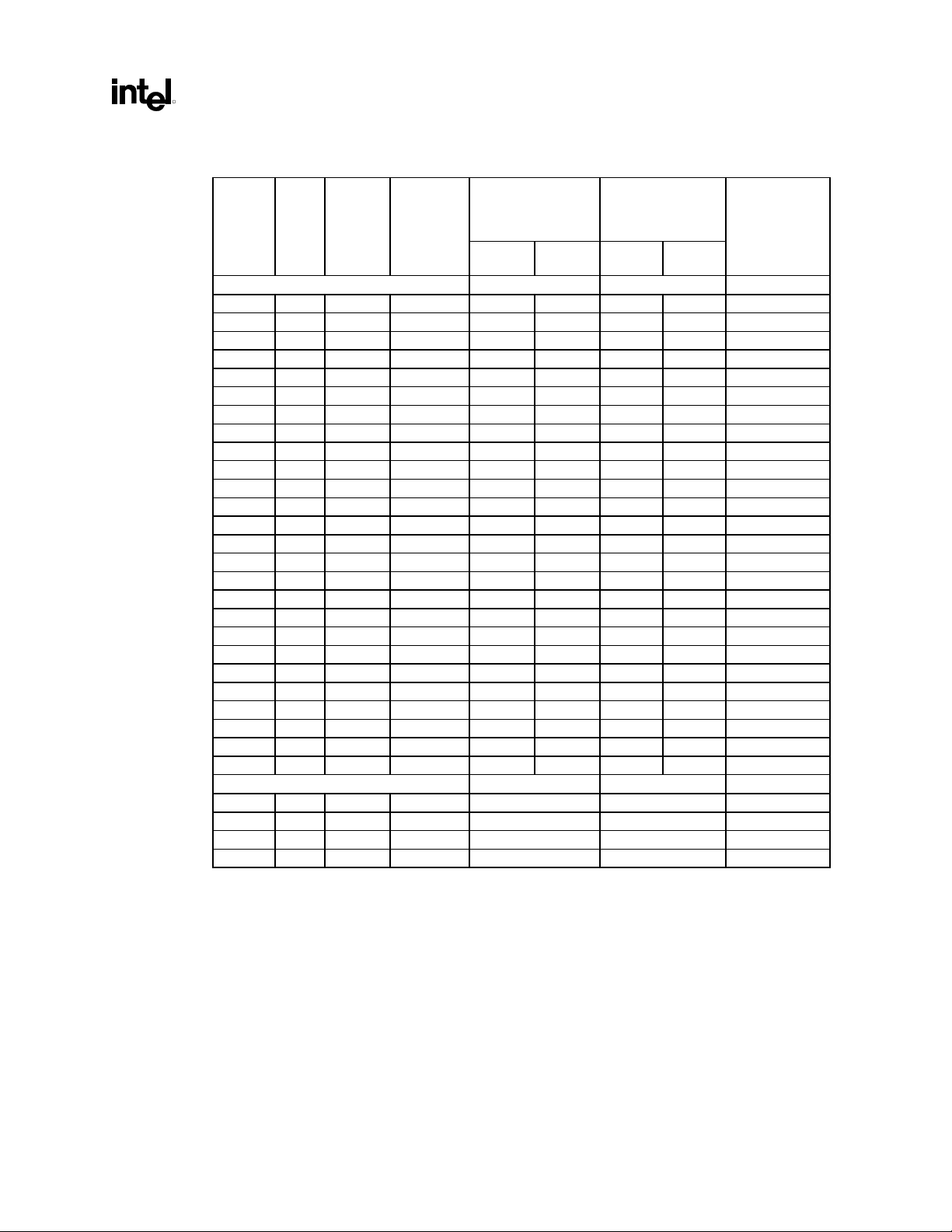
Intel® 820E Chipset
R
Table 8. Line Matching and Via Compensation Example
Signal Ball on
MCH
Min.
Formula A Formula B
DQA0 A13 2000 138.14 1851.86 1871.86 1876.86 1896.86 Top
DQA1 C13 2000 19.11 1970.89 1990.89 1995.89 2015.89 Bottom
DQA2 A14 2000 163.16 1826.84 1846.84 1851.84 1871.84 Top
DQA3 C14 2000 39.87 1950.13 1970.13 1975.13 1995.13 Bottom
DQA4 B14 2000 97.54 1892.46 1912.46 1917.46 1937.46 Top
DQA5 C15 2000 62.67 1927.33 1947.33 1952.33 1972.33 Bottom
DQA6 A15 2000 186.11 1803.90 1823.90 1828.90 1848.90 Top
DQA7 C16 2000 95.70 1894.30 1914.30 1919.30 1939.30 Bottom
DQA8 A16 2000 230.20 1759.81 1779.81 1784.81 1804.81 Top
DQB0 C7 2000 39.56 1950.44 1970.44 1975.44 1995.44 Bottom
DQB1 B7 2000 95.83 1894.17 1914.17 1919.17 1939.17 Top
DQB2 C6 2000 63.49 1926.51 1946.51 1951.51 1971.51 Bottom
DQB3 A6 2000 153.69 1836.31 1856.31 1861.31 1881.31 Top
DQB4 C5 2000 97.33 1892.67 1912.67 1917.67 1937.67 Bottom
DQB5 A5 2000 191.43 1798.57 1818.57 1823.57 1843.57 Top
DQB6 B5 2000 152.47 1837.53 1857.53 1862.53 1882.53 Bottom
DQB7 A4 2000 237.71 1752.29 1772.29 1777.29 1797.29 Top
DQB8 C4 2000 138.29 1851.71 1871.71 1876.71 1896.71 Bottom
RQ0 A7 2000 179.49 1810.51 1830.51 1835.51 1855.51 Top
RQ1 C8 2000 27.12 1962.88 1982.88 1987.88 2007.88 Bottom
RQ2 A8 2000 162.21 1827.79 1847.79 1852.79 1872.79 Top
RQ3 C9 2000 5.80 1984.20 2004.20 2009.20 2029.20 Bottom
RQ4 B9 2000 71.70 1918.30 1938.30 1943.30 1963.30 Top
RQ5 A9 2000 133.88 1856.12 1876.12 1881.12 1901.12 Bottom
RQ6 A10 2000 122.20 1867.81 1887.81 1892.81 1912.81 Top
RQ7 C10 2000 0.00 1990.00 2010.00 2015.00 2035.00 Bottom
FORMULA C FORMULA D
CFM A12 2000 132.37 1906.85 1932.37 Bottom
CFM# B12 2000 64.63 1976.02 2001.54 Bottom
CTM B11 2000 56.06 1984.76 2010.29 Top
CTM# A11 2000 126.34 1913.01 1938.53 Top
NOTES:
1. Signals connecting to side A of the RIMM connector (i.e., A1, A2, A3, etc.) should be routed on the top (primary
side) of the motherboard.
2. Signals connecting to side B of the RIMM connector should be routed on the bottom (solder side).
3. These trace lengths apply only from the MCH to the first RIMM. All signals must match exactly from RIMM to
RIMM.
4. Clock trace lengths include the 1.021 trace velocity factor.
5. Formula A min.: Motherboard trace = (Nominal RSL length – package dimension) – 10 mils
6. Formula A max.: Motherboard trace = (Nominal RSL length – package dimension) + 10 mils
7. Formula B min.: Motherboard trace = (Nominal RSL length – package dimension) – 10 mils + 25 mil
8. Formula B max.: Motherboard trace = (Nominal RSL length – package dimension) + 10 mils + 25 mils
9. Formula C: Motherboard trace = (Nominal RSL length – package dimension) × 1.021
10. Formula D: Motherboard trace = (Nominal RSL length – package dimension + 25 mils) × 1.021
Nominal
RSL
Length
(mils)
Package
Dimension
(mils)
Motherboard Trace
Length When
Routed on Bottom
(i.e., Real Via)
(mils)
1,2,3,4,5,6,7,8,9,10
Motherboard Trace
Routed on Top
(i.e., Dummy Via)
Max.
(mils)
Min.
(mils)
Length When
Max.
(mils)
Recommended
Routing
Design Guide 53
Page 54

Intel® 820E Chipset
R
2.7.3. Direct RDRAM* Reference Voltage
The Direct RDRAM reference voltage (RAMREF) must be generated as shown in Figure 32. The
RAMREF should be generated from a typical resistor divider using 2%-tolerance resistors. Additionally,
the RAMREF must be decoupled locally at each RIMM connector, at the resistor divider, and at the
MCH. Finally, as shown in Figure 32, a 100 Ω series resistor is required near the MCH. The RAMREF
signal should be routed with a 10 mil-wide trace.
Figure 32. RAMREF Generation Example Circuit
V
TERM
MCH
RAMREFA
RAMREFB
C4
0.1 µF 0 .1 µF
100 Ω
R3
C10
2.7.4. High-Speed CMOS Routing
• The high-speed CMOS signals (CMD & SCK) must be routed using 28 Ω traces. Using the
recommended stack-up, these signals will be 18 mils wide.
• The high-speed CMOS signals must be length-matched to the RSL signals within 1200 mils
(1.2 inches), because of a timing requirement between CMOS and RSL signals during NAP Exit and
PDN Exit.
R1
160 Ω 2%
R2
560 Ω 2%
R
I
M
M
C5
0.1 µF
C8
0.1 µF
R
I
M
M
ramref_generation.vsd
• The high-speed CMOS signals require termination as shown in Figure 33, as a result of the buffer
strengths in the MCH.
• The resistors must be 91 Ω pull-up and 39 Ω pull-down, and they must be 2% or better for S3 mode
reliability. The trace impedances remain 28 Ω.
54 Design Guide
Page 55

Intel® 820E Chipset
RIMM_0
RIMM_1
R
Figure 33. High-Speed CMOS Termination
Vterm
MCH
2.7.4.1. SIO Routing
The SIO signal must be routed from RIMM to RIMM, as shown in Figure 34. The SIO signal requires a
2.2 kΩ to 10 kΩ terminating resistor on the SOUT pin of the last RIMM. SIO is routed with a standard
5 mil-wide, 60 Ω trace. The motherboard routing lengths for the SIO signal are the same as those for
RSL signals. (See Figure 34.)
Figure 34. SIO Routing Example
R1
R2
high_spd_cmos_term
N
N
91 Ω
39 Ω
82820
MCH
SIN B36
A
0" - 3.50"
3
2
1
A36 SOUT
SIN B36
B
0.4" - 0.45"
3
2
1
A36 SOUT
sio_route.vsd
2.2KΩ 10KΩ
Design Guide 55
Page 56

Intel® 820E Chipset
R
2.7.4.2. Suspend-to-RAM Shunt Transistor
When an Intel 820E chipset system enters or exits Suspend to RAM, power will be ramping to the MCH
(i.e., it will be powering up or powering down). While power is ramping, the states of the MCH outputs
are not guaranteed. Therefore, the MCH could drive the CMOS signals and issue CMOS commands. One
of the commandsthe only one the RDRAMs will respond tois the power-down exit command. To
avoid the MCH inadvertently taking the RDRAMs out of power-down because the CMOS interface is
driven during power ramp, the SCK (CMOS clock) signal must be shunted to ground when the MCH is
entering and exiting Suspend to RAM. This shunting can be accomplished using the NPN transistor
shown in the circuit in Figure 35. The transistor should have a C
(i.e., MMBT3904LT1).
In addition, to match the electrical characteristics on the SCK signal, the CMD signal needs a dummy
transistor. This transistor’s base should be tied to ground (i.e., always turned off).
To minimize impedance discontinuities, the traces for CMD and SCK must have a neckdown from
18 mil traces to 5 mil traces, for 175 mils on either side of the SCK/CMD attach point, as shown in
Figure 35.
Figure 35. RDRAM CMOS Shunt Transistor
of 4 pF or less
OBO
PWROK
MCH
MCH
18 mils
wide
VCC5SBY
2N3904
18 mils
wide
5 mils
175 mils
175
mils
wide
5 mils
wide
175 mils
2N3904
175
mils
18 mils
wide
SCK
18 mils
wide
R
I
M
M
S
R
I
M
M
S
2N3904
CMD
rdram_cmos_shunt_tran.v
56 Design Guide
Page 57

Intel® 820E Chipset
R
2.7.5. Direct RDRAM* Clock Routing
Refer to Chapter 4 Clocking for the Intel 820E chipset platform’s Direct RDRAM clock routing
guidelines.
2.7.6. Direct RDRAM* Design Checklist
Use the following checklist as a final check to ensure that the motherboard incorporates solid design
practices. This list is only a reference. For correct operation, all of the design guidelines within this
document must be followed.
Table 9. Signal List
RSL Signals High-Speed
• DQA[8:0]
• DQB[8:0]
• RQ[7:0]
CMOS Signals
• CMD
• SCK
Serial
CMOS Signal
• SIO • CTM
• CTM#
• CFM
• CFM#
Clocks
• Ground isolation well grounded.
Via to ground every 0.5 inch around edge of isolation island
Via to ground every 0.5 inch between RIMMs
Via to ground every 0.5 inch between signals (from MCH to first RIMM)
Via between every signal within 100 mils of the MCH edge and the connector edge
No unconnected ground floods
All ground isolation at least 10 mils wide.
Ground isolation fills between serpentines
Ground isolation not broken by C-TABs.
Ground isolation connects to the ground pins in the middle of the RIMM connectors.
Ground isolation vias connect on all 4 layers and should not have thermal reliefs.
Ground pins in RIMM connector connect on all 4 layers.
• V
layout yields low noise.
TERM
Solid V
Ground island (for ground side of V
Termination resistors connect directly to the V
Decoupling V
island is on top layer. Do not split this plane.
TERM
caps) is on top.
TERM
TERM
is critical!
TERM
island on the top layer (without vias).
Decoupling capacitors connect directly to top-layer V
island and top-layer ground island.
TERM
(See the layout example.)
Use at least 2 vias per decoupling capacitor in the top-layer ground island.
Use 2 × 100 µF tantalum capacitors to decouple V
. (Aluminum/electrolytic capacitors are
TERM
too slow!)
High-frequency decoupling capacitors must be spread out across the termination island so that
all termination resistors are near high-frequency capacitors.
100 µF tantalum capacitors should be at each end of the V
100 µF tantalum capacitors must be connected directly to V
TERM
TERM
island.
island.
100 µF tantalum capacitors must have at least 2 vias/cap to ground.
V
V
island should be 50–75 mils wide.
TERM
island should not be broken.
TERM
Design Guide 57
Page 58

Intel® 820E Chipset
R
If any RSL signals are routed, even for a short distance, out of the last RIMM (towards
termination) on the bottom side, ensure that the ground reference plane (on the third layer) is
continuous under the termination resistors/capacitors.
Ensure that the current path for power delivery to the MCH does not go through the V
TERM
island.
• CTM/CTM# routed properly
CTM/CTM# are routed differentially from DRCG to last RIMM.
CTM/CTM# are ground-isolated from DRCG to last RIMM.
CTM/CTM# are ground-referenced from DRCG to last RIMM.
Vias are placed in ground isolation and ground reference every 0.5 inch.
When CTM/CTM# serpentine together, they MUST maintain exactly 6 mils of spacing.
• Clean DRCG power supply
The 3.3 V DRCG power flood on the top layer should connect to each high-frequency (0.1 µF)
capacitor, to the 10 µF bulk tantalum capacitor, and to the ferrite bead.
High-frequency (0.1 µF) capacitors are near the DRCG power pins, with one capacitor next to
each power pin.
10 µF bulk tantalum capacitor near DRCG connected directly to the 3.3 V DRCG power flood
on the top layer
The ferrite bead isolating the DRCG power flood from the 3.3 V main power also connects
directly to the 3.3 V DRCG power flood on the top layer.
Use 2 vias on the ground side of each.
• Good DRCG output network layout
Series resistors (39 Ω) should be very near CTM/CTM# pins.
Parallel resistors (51 Ω) should be very near series resistors.
CTM/CTM# should be 18 mils wide, from the CTM/CTM# pins to the resistors.
CTM/CTM# should be 14-on-6 routed differentially as close as possible after the resistor
network.
When not 14 on 6, the clocks should be 18 mils wide.
Ensure that CTM/CTM# are ground-referenced and the ground reference is connected to the
ground plane every 0.5 inch to 1 inch.
Ensure that CTM/CTM# are ground-isolated and the ground isolation is connected to the
ground plane every 0.5 inch to 1 inch.
Ensure that 15 pF EMI capacitors to ground are removed. (The pads are not necessary, and
removing the pads provides more space for better placement of other components.)
Ensure the that 4 pF-EMI capacitor is implemented (but do not assemble the capacitor).
• Good RSL transmission lines
RSL traces are 18 mils wide.
When RSL traces neck down to exit the MCH BGA, the minimum width is 15 mils and the
neckdown is no longer than 25 mils in length.
RSL traces do not neck down when routing into the RIMM connector.
If tight serpentining is necessary, 10 mil ground isolation must be between serpentine
segments. (i.e., an RSL signal cannot serpentine so tightly that the signal is adjacent to itself
with no ground isolation between the serpentines.)
RSL traces do not cross power plane splits. RSL signals also must not be routed next to a
power plane split. (For example, the RSL signals on the 4
below the ground isolation split on the 3
rd
layer.)
th
layer cannot be routed directly
At all times, uniform ground isolation flood is exactly 6 mils from the RSL signals.
ALL RSL, CMD/SCK, and CTM/CTM#/CFM/CFM# signals have CTABs on each RIMM
connector pin.
58 Design Guide
Page 59

Intel® 820E Chipset
R
All RSL signals are routed adjacent to a ground reference plane. This includes all signals from
the last RIMM to the termination. If signals are routed on the bottom from the last RIMM to
the termination, the ground reference plane on the 3
and include the ground side of the V
decoupling capacitors.
TERM
rd
layer must extend under these signals
CTABs must not cross (or be on top of) power plane splits. They must be entirely referenced
to ground.
At least 10 mils of ground flood isolation is required around all RSL signals. (Ground isolation
must be exactly 6 mils from RSL signals.) Ground flood is recommended for isolation. This
ground flood should be as close as possible to the MCH (and the first RIMM). If possible,
connect the flood to the ground balls/pins on the MCH/connector.
• Clean V
Ensure a 1 × 0.1 µF capacitor on V
routing
REF
at each connector.
REF
Use a 10 mil-wide trace (6 mils minimum).
Do not route V
near high-speed signals.
REF
• RSL routing
All signals must be length-matched within ±10 mils of the nominal RSL length. (Note: Use the
®
table in the Intel
820 Chipset Family: 82820 Memory Controller Hub (MCH) Datasheet to
verify the trace lengths.) Ensure that signals with a dummy via are compensated correctly.
ALL RSL signals must have one via near the MCH BGA pad. Signals routed on the secondary
side of the MB will have a “real via,” while signals routed on the primary side will have a
“dummy via.” Additionally, all signals with a dummy via must have an additional trace length
of 25 mils.
B-side RIMM connector signals are routed on the secondary side of the motherboard. A-side
RIMM connector signals are routed on the primary side of the motherboard.
Signals must “alternate” layers, as shown in the following table:
If Signal Routed from MCH
to 1st RIMM on:
Primary side Secondary side
Secondary side Primary side
Then Route Signal from 1st RIMM
to Next RIMM on:
• Clock routing
Clock signals must be routed as a differential pair. The traces must be 14 mils wide and 6 mils
apart (with no ground isolation) when they are routed as a differential pair. For very short
sections under the MCH and under the first RIMM, it will not be possible to route as a
differential pair. In these sections, the clocks signals must neck up to 18 mils and be ground-
isolated with at least 10 mils ground isolation.
Clock signals must be length-compensated (using the 1.021 length factor mentioned in Section
2.8.3 2×/4× Timing Domain Routing Guidelines, 2×/4× Timing Domain Routing Guidelines).
Ensure that each clock pair is length-matched within ±2 mils.
When clock signals serpentine, they must serpentine together (to maintain differential 14:6
routing).
22 mil ground isolation is required on each side of the differential pair.
Design Guide 59
Page 60

Intel® 820E Chipset
R
2.8. AGP 2.0
For detailed AGP interface functionality (e.g., protocols, rules, signaling mechanisms), refer to Revision
2.0 of the latest AGP Interface Specification obtainable from http://www.agpforum.org
focuses only on specific Intel 820E chipset platform recommendations.
Revision 2.0 of the AGP Interface Specification enhances the functionality of the original AGP Interface
Specification (Rev. 1.0) by allowing 4× data transfers (4 data samples per clock) and 1.5 V operation. In
addition to these major enhancements, additional performance enhancement and clarifications (e.g., fast-
write capability) are included in the AGP Interface Specification (Rev. 2.0). The Intel 820E chipset
supports the enhanced features of AGP 2.0.
The 4× operation of the AGP interface provides for “quad-pumping” of the AGP AD (address/data) and
SBA (side-band addressing) buses. That is, data is sampled four times during each 66 MHz AGP clock.
This means that each data cycle is ¼ of a 15-ns (66 MHz) clock, or 3.75 ns. It is important to realize that
3.75 ns is the data cycle time, not the clock cycle time. During 2× operation, data is sampled twice during
a 66 MHz clock cycle. Therefore, the data cycle time is 7.5 ns.
To allow for these high-speed data transfers, the 2× mode of AGP operation uses source-synchronous
data strobing. (Refer to Source-Synchronous Strobing section.) During 4× operation, the AGP interface
uses differential source-synchronous strobing.
. This document
With data cycle times as small as 3.75 ns and setup/hold times of 1 ns, the propagation delay mismatch is
critical. In addition to reducing propagation delay mismatch, it is important to minimize noise. Noise on
the data lines will cause the settling time to be long. If the mismatch between a data line and the
associated strobe is too great or if there is noise on the interface, incorrect data will be sampled.
The low-voltage operation on AGP (1.5 V) requires even more noise immunity. For example, during
1.5 V operation, V
is 570 mV. Without proper isolation, crosstalk could create signal integrity
ILMAX
issues.
2.8.1. AGP Interface Signal Groups
The signals on the AGP interface are broken into three groups: 1× timing domain signals, 2×/4× timing
domain signals, and miscellaneous signals. Each group has different routing requirements. In addition,
within the 2×/4× timing domain signals, there are three sets of signals. All signals in the 2×/4× timing
domains must meet minimum and maximum trace length requirements as well as trace width and spacing
requirements. However, trace length matching requirements only must be met within each set of 2×/4×
timing domain signals.
60 Design Guide
Page 61

Intel® 820E Chipset
R
Signal Groups
• 1× timing domain
CLK (3.3 V)
RBF#
WBF#
ST[2:0]
PIPE#
REQ#
GNT#
PAR
FRAME#
IRDY#
TRDY#
STOP#
DEVSEL#
• 2×/4× timing domains
Set 1
AD[15:0]
C/BE[1:0]#
AD_STB0
AD_STB0# (used in 4× mode only)
Set 2
AD[31:16]
C/BE[3:2]#
AD_STB1
AD_STB1# (used in 4× mode only)
Set 3
SBA[7:0]
SB_STB
SB_STB# (used in 4× mode only)
• Miscellaneous, async
USB+
USB-
OVRCNT#
PME#
TYPDET#
PERR#
SERR#
INTA#
INTB#
Design Guide 61
Page 62

Intel® 820E Chipset
R
Table 10. AGP 2.0 Data/Strobe Associations
Data Associated Strobe in 1× Associated
AD[15:0] and
C/BE[1:0]#
AD[31:16]
and
C/BE[3:2]#
SBA[7:0] Strobes are not used in 1× mode. All data is
Strobes are not used in 1× mode. All data is
sampled on rising clock edges.
Strobes are not used in 1× mode. All data is
sampled on rising clock edges.
sampled on rising clock edges.
Throughout this chapter, the term “data” refers to AD[31:0], C/BE[3:0]#, and SBA[7:0]. The term
“strobe” refers to AD_STB[1:0], AD_STB#[1:0], SB_STB, and SB_STB#. When the term data is used,
it refers to one of the three sets of data signals. When the term strobe is used, it refers to one of the
strobes as it relates to the data in its associated group.
The routing guidelines for each group of signals (1× timing domain signals, 2×/4× timing domain signals,
and miscellaneous signals) will be discussed separately.
2.8.2. 1× Timing Domain Routing Guidelines
• The AGP 1× timing domain signals have a maximum trace length of 7.5 inches. (Refer to signal
groups listed previously.) This maximum applies to all signals listed as 1× timing domain signals in
the Signal Groups section.
Strobe in 2×
AD_STB0 AD_STB0, AD_STB0#
AD_STB1 AD_STB1, AD_STB1#
SB_STB SB_STB, SB_STB#
Associated Strobes
in 4×
• AGP 1× timing domain signals can be routed with 5 mil minimum trace separation.
• There are no trace length matching requirements for 1× timing domain signals.
2.8.3. 2×/4× Timing Domain Routing Guideli nes
These trace length guidelines apply to all signals listed as 2×/4× timing domain signals. These signals
should be routed using 5 mil (60 Ω) traces.
The maximum line length and length mismatch requirements depend on the routing rules used on the
motherboard. These routing rules were created to allow design freedom by making tradeoffs between
signal coupling (trace spacing) and line lengths. The maximum length of the AGP interface defines which
set of routing guidelines must be used. Guidelines for short AGP interfaces (e.g., < 6 inches) and long
AGP interfaces (e.g., > 6 inches and < 7.25 inches) are documented separately. The maximum allowable
length of the AGP interface is 7.25 inches.
Interfaces < 6 Inches
If the AGP interface is less than 6 inches, a minimum 1:3 trace spacing is required for 2×/4× lines (data
and strobes). These 2×/4× signals must be matched to their associated strobe, within ±0.5 inch. These
guidelines are for designs that require less than 6 inches between the AGP connector and the MCH.
For example, if a set of strobe signals (e.g., AD_STB0 and AD_STB0#) are 5.3 inches long, the data
signals associated with those strobe signals (e.g., AD[15:0] and C/BE[2:0]#) can be 4.8 inches to
62 Design Guide
Page 63

Intel® 820E Chipset
R
5.8 inches long. Another strobe set (e.g., SB_STB and SB_STB#) could be 4.2 inches long, and the data
signals associated with those strobe signals (e.g., SBA[7:0]) can be 3.7 inches to 4.7 inches long.
The strobe signals (AD_STB0, AD_STB0#, AD_STB1, AD_STB1#, SB_STB, and SB_STB#) act as
clocks on the source-synchronous AGP interface. Therefore, special care must be taken when routing
these signals. Because each strobe pair is truly a differential pair, the pair should be routed together. (For
example, AD_STB0 and AD_STB0# should be routed next to each other.) The two strobes in a strobe
pair should be routed on 5 mil traces, with at least 15 mils of space (1:3) between them. This pair should
be separated from the rest of the AGP signals (and all other signals) by at least 20 mils (1:4). The strobe
pair must be length-matched to less than ±0.1 inch. (That is, a strobe and its complement must be the
same length, within 0.1 inch.)
Figure 36. AGP 2×/4× Routing Example for Interfaces < 6 Inches
5-mil trace
5-mil trace
5-mil trace
5-mil trace
5-mil trace
15 mils
20 mils
15 mils
20 mils
15 mils
2X/4X signal
2X/4X signal
AGP STB#
AGP STB
2X/4X signal
2X/4X signal
STB/STB# length
Associated AGP 2X/4X data signal length
Min. Max.
0.5" 0.5"
2X/4X signal
2X/4X signal
AGP STB#
AGP STB
2X/4X signal
2X/4X signal
AGP_2x-4x_routing
Interfaces > 6 Inches and < 7.25 Inches
Longer lines have more crosstalk. Therefore, to reduce skew, longer line lengths require a greater amount
of spacing between traces. For line lengths greater than 6 inches and less than 7.25 inches, 1:4 routing is
required for all data lines and strobes. For these designs, the line length mismatch must be less than
±0.125 inch within each signal group (between all data signals and the strobe signals).
For example, if a set of strobe signals (e.g., AD_STB0 and AD_STB0#) are 6.5 inches long, the data
signals associated with those strobe signals (e.g., AD[15:0] and C/BE[2:0]#) can be 6.475 inches to
6.625 inches long. Another strobe set (e.g., SB_STB and SB_STB#) could be 6.2 inches long, and the
data signals associated with those strobe signals (e.g., SBA[7:0]) can be 6.075 inches to 6.325 inches
long.
Design Guide 63
Page 64

Intel® 820E Chipset
R
The strobe signals (AD_STB0, AD_STB0#, AD_STB1, AD_STB1#, SB_STB, and SB_STB#) act as
clocks on the source-synchronous AGP interface. Therefore, special care must be taken when routing
these signals. Because each strobe pair is truly a differential pair, the pair should be routed together. (For
example, AD_STB0 and AD_STB0# should be routed next to each other.) The two strobes in a strobe
pair should be routed on 5 mil traces with at least 20 mils of space (1:4) between them. This pair should
be separated from the rest of the AGP signals (and all other signals) by at least 20 mils (1:4). The strobe
pair must be length-matched to less than ±0.1 inch. (i.e., a strobe and its complement must be the same
length, within 0.1 inch.)
All AGP Interfaces
The 2×/4× timing domain signals can be routed with 5 mil spacing when breaking out of the MCH. The
routing must widen to the documented requirements within 0.3 inch of the MCH package.
When matching the trace length for the AGP 4× interface, all traces should be matched from the ball of
the MCH to the pin on the AGP connector. It is not necessary to compensate for the length of the AGP
signals on the MCH package.
Reduce line length mismatch to ensure added margin. To reduce trace-to-trace coupling (crosstalk),
separate the traces as much as possible. All signals in a signal group should be routed on the same layer.
The trace length and trace spacing requirements must not be violated by any signal. Trace length
mismatch for all signals within a signal group should be as close to zero as possible, to provide timing
margin.
2.8.4. AGP 2.0 Routing Summary
Table 11. AGP 2.0 Routing Summary
Signal Maximum
Length
(inches)
1× Timing
Domain
2×/4× Timing
Domain Set 1
2×/4× Timing
Domain Set 2
2×/4× Timing
Domain Set 3
2×/4× Timing
Domain Set 1
2×/4× Timing
Domain Set 2
2×/4× Timing
Domain Set 3
NOTES:
1. Each strobe pair must be separated from other signals by at least 20 mils.
2. These guidelines apply to board stack-ups with 10% impedance tolerance.
7.5 5 mils No
7.25 20 mils ±0.125 AD_STB0 and
7.25 20 mils ±0.125 AD_STB1 and
7.25 20 mils ±0.125 SB_STB and
6 15 mils1 ±0.5 AD_STB0 and
6 15 mils1 ±0.5 AD_STB1 and
6 15 mils1 ±0.5 SB_STB and
1,2
Trace Spacing
(5 mil Traces)
Length
Mismatch
(inches)
requirement
Relative To Notes
N/A None
AD_STB0 and AD_STB0#
AD_STB0#
AD_STB1#
SB_STB#
AD_STB0#
AD_STB1#
SB_STB#
must be the same length.
AD_STB1 and AD_STB1#
must be the same length.
SB_STB and SB_STB# must
be the same length.
AD_STB0 and AD_STB0#
must be the same length.
AD_STB1 and AD_STB1#
must be the same length.
SB_STB and SB_STB# must
be the same length.
64 Design Guide
Page 65

Intel® 820E Chipset
R
2.8.5. AGP Clock Routing
The maximum total AGP clock skew (between the MCH and the graphics component) is 1 ns for all data
transfer modes. This 1 ns includes skew and jitter that originates on the motherboard, add-in card, and
clock synthesizer. Clock skew must be evaluated not only at a single threshold voltage, but at all points
on the clock edge that fall within the switching range. The 1-ns skew budget is divided such that the
motherboard is allotted 0.9 ns of clock skew. (The motherboard designer determines how the 0.9 ns are
allocated between the board and the synthesizer.) For the Intel 820E chipset platform’s AGP clock
routing guidelines, refer to Chapter 4 Clocking.
2.8.6. General AGP Routing Guidelines
The following routing guidelines are recommended for the optimal system design. The main focus of
these guidelines is the minimization of signal integrity problems on the AGP interface of the Intel 820E
chipset’s MCH. The following guidelines are not intended to replace thorough system validation on Intel
820E chipset-based products.
2.8.6.1. Recommendations
Decoupling
• For V
within 70 mils of the outer row of balls on the MCH. (See Figure 37.)
• Evenly distribute the placement of decoupling capacitors in the AGP interface signal field.
• Use a low-ESL ceramic capacitor (e.g., 0603 body type, X7R dielectric).
• In addition to the minimum decoupling capacitors, bypass capacitors should be placed at vias that
transition AGP signals from one reference signal plane to another. In a typical four-layer PCB
design, the signals transition from one side of the board to the other.
• One extra 0.01-µF capacitor is required per 10 vias. The capacitor should be placed as close as
possible to the center of the via field.
• Ensure that the AGP connector is well decoupled, as described in the AGP Design Guide, Revision
1.0 (Section 1.5.3.3).
Note: To add the decoupling capacitors as close as possible to the MCH and/or close to the vias, the trace
spacing may be reduced as the traces go around each capacitor. The narrowing of the space between
traces should be minimal and for as short a distance as possible (1 inch max.).
decoupling, at least six 0.01-µF capacitors are required, of which at least four must be
DDQ
Design Guide 65
Page 66

Intel® 820E Chipset
R
Figure 37. Top Signal Layer
2.8.7. V
Ground Reference
It is strongly recommended that, at a minimum, the following critical signals be referenced to ground
from the MCH to an AGP connector (or to an AGP video controller, if implemented as a “down”
solution), utilizing a minimum number of vias on each net: AD_STB0, AD_STB0#, AD_STB1,
AD_STB1#, SB_STB, SB_STB#, G_GTRY#, G_IRDY#, G_GNT#, and ST[2:0].
In addition to the minimum signal set listed previously, it is strongly recommended that half of all AGP
signals be referenced to ground, depending on the board layout. In the ideal design, the entire AGP
interface signal field would be referenced to ground.
DDQ
was
CC
These recommendations are not specific to any particular PCB stack-up, but are applicable to all Intel
chipset designs.
Generation and TYPEDET#
DDQ
AGP specifies two separate power planes (VCC and V
controller. V
is always 3.3 V. V
CC
is the interface voltage. In AGP 1.0 implementations, V
DDQ
). VCC is the core power for the graphics
DDQ
also 3.3 V. For the designer developing an AGP 1.0 motherboard, there is no distinction between V
and V
, because both are tied to the 3.3 V power plane on the motherboard.
DDQ
AGP 2.0 requires that these power planes be separate. In conjunction with the 4× data rate, the AGP 2.0
interface specification provides for low-voltage (1.5 V) operation. The AGP 2.0 specification
implements a TYPEDET# (type detect) signal on the AGP connector that determines the operating
voltage of the AGP 2.0 interface (V
). The motherboard must provide either 1.5 V or 3.3 V to the
DDQ
add-in card, depending on the state of the TYPEDET# signal. (Refer to Table 12.) 1.5 V low-voltage
). V
operation applies only to the AGP interface (V
DDQ
is always 3.3 V.
CC
66 Design Guide
Page 67

Intel® 820E Chipset
R
Note: The motherboard provides 3.3 V to the V
lower voltage, then the add-in card must regulate the 3.3 V V
The graphics controller may only power AGP I/O buffers with the V
The TYPEDET# signal indicates whether the AGP 2.0 interface operates at 1.5 V or 3.3 V. If
TYPEDET# is floating (i.e., no connect) on an AGP add-in card, the interface is 3.3 V. If TYPEDET# is
shorted to ground, the interface is 1.5 V.
Table 12. TYPDET#/V
TYPEDET# (on Add-in Card) V
Relationship
DDQ
DDQ
GND 1.5 V
N/C 3.3 V
As a result of this requirement, the motherboard must provide a flexible voltage regulator. This regulator
must supply the appropriate voltage to the V
recommendations, refer to the schematics in Appendix A: Reference Design Schematics (Uniprocessor).
V
generation and AGP V
DDQ
generation must be considered together. Before developing V
REF
generation circuitry, refer to the AGP 2.0 Interface Specification.
Figure 38 demonstrates one way to design the V
with an external, low-R
FET. The source of the FET is connected to 3.3 V. This regulator will
DS-ON
convert 3.3 V to 1.5 V or pass 3.3 V, depending on the state of TYPEDET#. If a linear regulator is used,
it must draw power from 3.3 V (not 5 V) to control thermals. (i.e., 5 V regulated down to 1.5 V with a
linear regulator will dissipate approximately 7 W at 2 A.) Because it must draw power from 3.3 V and, in
some situations, must simply pass that 3.3 V to V
the regulator must use a low-R
DS-ON
pins of the AGP connector. If the graphics controller needs a
CC
(Supplied by MB)
pins on the AGP connector. For specific design
DDQ
DDQ
DDQ
FET.
voltage to the controller’s requirements.
CC
power pins.
DDQ
DDQ
voltage regulator. This regulator is a linear regulator
(when a 3.3 V add-in card is placed in the system),
AGP 1.0 modified V
Therefore, 68 mV of drop is allowed across the FET at 2 A. This corresponds to an FET with an R
DDQ
3.3
to 3.1 V. When an ATX power supply is used, the 3.3 V
MIN
is 3.168 V.
MIN
DS-ON
of 34 mW.
How does the regulator switch? The feedback resistor divider is set to 1.5 V. When a 1.5 V card is
placed in the system, the transistor is off and the regulator regulates to 1.5 V. When a 3.3 V card is
placed in the system, the transistor is on and the feedback is pulled to ground. When this happens, the
regulator drives the gate of the FET to nearly 12 V. This turns on the FET and passes
3.3 V – 2 A × R
DS-ON
to V
DDQ
.
Design Guide 67
Page 68

Intel® 820E Chipset
R
Figure 38. AGP V
TYPEDET#
Generation Example Circuit
DDQ
+12V
O
R1
1 k
Ω
C1
1 µF
U1
LT1575
1
SHDN IPOS
2
VIN INEG
3
GND GATE
4
FB COMP
47 µF
+3.3V
O
C2
47 µF
5
6
7
8
C4
10 pF
R5
C5
7.5 k
Ω
5
Ω
R2
R3
301
R4
1.21 k
C3
220 µF
Ω
Ω
VDDQ
O
agp_vddq_generati on.vsd
2.8.8. V
Generation for AGP 2.0 (2× and 4×)
REF
V
generation for AGP 2.0 will differ, depending on the AGP card type used. The 3.3 V AGP cards
REF
generate V
shown in Figure 39. To account for potential differences between V
graphics controller, 1.5 V cards use a source-generated V
graphics controller and sent to the MCH, and another V
locally (i.e., they have a resistor divider on the card that divides V
REF
and GND at the MCH and
DDQ
. (i.e., the V
REF
is generated at the MCH and sent to the
REF
down to V
DDQ
signal is generated at the
REF
REF
), as
graphics controller.).
Both the graphics controller and the MCH are required to generate V
and distribute it through the
REF
connector (1.5 V add-in cards only). Two pins are defined on the AGP 2.0 universal connector to allow
this V
To preserve the common-mode relationship between the V
V
passing, as follows:
REF
• VREFGC: V
• VREFCG: V
signals must be matched in length to the strobe lines, within 0.5 inch on the motherboard and within
REF
from the graphics controller to the chipset
REF
from the chipset to the graphics controller
REF
REF
and data signals, the routing of the two
0.25 inch on the add-in card.
The voltage-divider networks consist of AC and DC elements, as shown in Figure 39.
The V
benefit of the common-mode power supply. However, the trace spacing around the V
divider network should be placed as close as practical to the AGP interface, to obtain the
REF
signals must be
REF
a minimum of 25 mils, to reduce crosstalk and maintain signal integrity.
68 Design Guide
Page 69

Intel® 820E Chipset
R
During a 3.3 V AGP 2.0 operation, V
V
must be 0.5 V
REF
accomplishing this exist, such as the example in the following figure.
Figure 39. AGP 2.0 V
1.5-V AGP Card
Notes :
1. The resistor dividers should be placed near the GMCH. The AGPREF s ignal must be 5 mils wide and routed 10 mil s from adjacent signal s.
2. R7 is the sam e resistor as R1 in the figure AGP VDDQ Generation Example Circui t.
must be 0.4 V
REF
. This requires a flexible voltage divider for V
DDQ
Generation and Distribution
REF
+12 V
R7
(Note 2)
1 k
Ω
TYPEDET#
VrefGC
VDDQ
AGP
REF
device
GND
VrefCG
MOSFET
. However, during a 1.5 V AGP 2.0 operation,
DDQ
U6
Place C10 close to MCH.
. Various methods of
REF
300
R11
200
C10
0.1 µF
R9
Ω
Ω
1%
1%
REF
VDDQ
VDDQ
GMCH
GND
1 k
1 k
R6
R2
C8
500 pF
Ω
Ω
R5
82
R4
Ω
82
C9
500 pF
Ω
+12 V
(Note 2)
R7
1 k
Ω
3.3-V AGP Card
VDDQ
AGP
REF
device
GND
Notes :
1. The resistor dividers should be placed near the GMCH. The AGPREF s ignal must be 5 mils wide and routed 25 mil s from adjacent signal s.
2. R7 is the sam e resistor as R1 in the figure AGP VDDQ Generation Example Circui t.
The flexible V
generated V
divider shown in the preceding figure uses an FET switch to switch between the locally
REF
(for 3.3 V add-in cards) and the source-generated V
REF
Use of the source-generated V
TYPEDET#
VrefGC
U6
MOSFET
Place C10 close to MCH.
VrefCG
at the receiver is optional and is a product implementation issue
REF
R9
300
Ω
1%
R11
200
Ω
1%
C10
0.1 uF
(for 1.5 V add-in cards).
REF
REF
VDDQ
VDDQ
GMCH
GND
R6
1 k
Ω
R2
R4
Ω
1 k
82
Ω
C9
500 pF
AGP2_Vref_gen-dist
beyond the scope of this document.
500 pF
R5
82
C8
Ω
Design Guide 69
Page 70

Intel® 820E Chipset
R
2.8.9. Compensation
The MCH AGP interface supports resistive buffer compensation (RCOMP). Tie the GRCOMP pin to a
40 Ω, 2% (or 39-Ω, 1%) pull-down resistor (to ground), via a 10 mil-wide, very short (<0.5 inch) trace.
2.8.10. AGP Pull-Ups
AGP control signals require pull-up resistors to V
DDQ
stable values when no agent is actively driving the bus. The signals requiring pull-up resistors are:
• 1× timing domain signals
FRAME#
TRDY#
IRDY#
DEVSEL#
STOP#
SERR#
PERR#
RBF#
PIPE#
REQ#
WBF#
GNT#
ST[2:0]
It is critical that these signals be pulled up to V
The trace stub to the pull-up resistor on 1× timing domain signals should be kept at less than
0.5 inch, to avoid signal reflections from the stub.
The strobe signals require pull-up/pull-downs on the motherboard, to ensure that they maintain
stable values when no agent is driving the bus.
Note: INTA# and INTB# should be pulled to 3.3 V, not V
• 2×/4× timing domain signals
AD_STB[1:0] (pull-up to V
SB_STB (pull-up to V
DDQ
DDQ
)
)
AD_STB[1:0]# (pull-down to ground)
SB_STB# (pull-down to ground)
The trace stub to the pull-up/pull-down resistor on 2×/4× timing domain signals should be kept to
less than 0.1 inch, to avoid signal reflections from the stub.
The pull-up/pull-down resistor value requirements are shown in the following table.
R
R
MIN
MAX
on the motherboard, to ensure that they maintain
(not 3.3 V).
DDQ
.
DDQ
4 kΩ 16 kΩ
The recommended AGP pull-up/pull-down resistor value is 8.2 kΩ.
70 Design Guide
Page 71

Intel® 820E Chipset
R
2.8.10.1. AGP Signal Voltage Tolerance List
The following signals on the AGP interface are 3.3 V tolerant during a 1.5 V operation:
• PME#
• INTA#
• INTB#
• GPERR#
• GSERR#
• CLK
• RST
The following signals on the AGP interface are 5 V tolerant (refer to the USB specification):
• USB+
• USB-
• OVRCNT#
The following signal is a special AGP signal, which is either grounded or not connected on an AGP card.
• TYPEDET#
Note: All other signals on the AGP interface are in the V
group. They are not 3.3 V tolerant during a 1.5 V
DDQ
AGP operation.
2.8.11. Motherboard / Add-in Card Interoperability
Currently, there are three AGP connectors:
• 3.3 V AGP connector
• 1.5 V AGP connector
• Universal AGP connector.
To maximize add-in flexibility, it is highly advisable to implement the universal connector in an Intel
820E chipset-based system. All add-in cards are either 3.3 V or 1.5 V cards. Due to timings, 4× transfers
at 3.3 V are not allowed.
Table 13. Connector / Add-in Card Interoperability
1.5 V Connector 3.3 V Connector Universal Connector
1.5 V card Yes No Yes
3.3 V card No Yes Yes
Table 14. Voltage / Data Rate Interoperability
1× 2× 4×
1.5 V V
3.3 V V
Yes Yes Yes
DDQ
Yes Yes No
DDQ
Design Guide 71
Page 72

Intel® 820E Chipset
R
2.8.12. AGP Universal Retention Mechanism (RM)
Environmental testing and field reports indicate that, without proper retention, AGP cards and AGP
In-Line Memory Module (AIMM) cards may come unseated during system shipping and handling. In
order to prevent the disengagement of AGP cards and AIMM modules, Intel recommends that AGPbased platforms use the AGP retention mechanism (RM).
The AGP RM is a mounting bracket used to properly locate the card with respect to the chassis and to
assist with card retention. The AGP RM is available in two different handle orientations: left-handed (see
Figure 40) and right-handed. Most system boards accommodate the left-handed AGP RM. Because the
manufacturing capacity is greater for the left-handed RM, Intel recommends that customers design into
their systems the left-handed AGP RM (Figure 41). The right-handed AGP RM is identical to the lefthanded AGP RM, except for the position of the actuation handle, which is located on the same end as in
the primary design, but extends from the opposite side, parallel to the longitudinal axis of the part. Figure
41 details the keep-out information for the left-handed AGP RM. Use this information to ensure that your
motherboard design leaves adequate space for RM installation.
The AGP interconnect design requires that the AGP card be retained so as to limit card back-out within
the AGP connector to 0.99 mm (0.039 in.) max. For this reason, new cards should have an additional
mechanical keying tab notch, which provides an anchor point on the AGP card for interfacing with the
AGP RM. The RM’s round peg engages with the AGP or AIMM card’s retention tab, thereby preventing
the card from disengaging during dynamic loading. The additional notch in the mechanical keying tab is
required for 1.5 V AGP cards and is recommended for the new 3.3 V AGP cards.
Figure 40. AGP Left-Handed Retention Mechanism
72 Design Guide
Page 73

Intel® 820E Chipset
R
Figure 41. AGP Left-Handed RM Keep-Out Information
Recommended for all AGP cards, the AGP RM is detailed in Engineering Change Request No. 48
(ECR #48), which details approved changes to the Accelerated Graphics Port (AGP) Interface
Specification, Revision 2.0. Intel intends to incorporate the AGP RM changes into later revisions of the
AGP interface specification. In addition, Intel has defined a reference design for a mechanical device
utilizing the features defined in ECR #48.
ECR #48 can be viewed on the Intel Web site at: http://developer.intel.com/technology/agp/ecr.htm
More information regarding this component (AGP RM) is available from the following vendors:
Resin Color Supplier Part No. “Left-Handed” Orientation
(Preferred)
AMP P/N 136427-1 136427-2 Black
Foxconn P/N 006-0002-939 006-0001-939
Green Foxconn P/N 009-0004-008 009-0003-008
“Right-Handed” Orientation
(Alternate)
Design Guide 73
Page 74
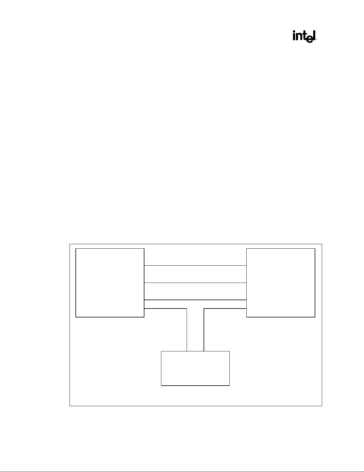
Intel® 820E Chipset
R
2.9. Hub Interface
The MCH and ICH2 ballout assignments have been optimized to simplify the hub interface routing
between these devices. It is recommended that the hub interface signals be routed directly from the MCH
to ICH2, with all signals referenced to V
change is required, use only two vias per net and keep all data signals and associated strobe signals on
the same layer. The hub interface is broken into two signal groups: data signals and strobe signals. These
groups are:
• Data signal
HL[10:0]
• Strobe signals
HL_STB
HL_STB#
Note: HL_STB/HL_STB# is a differential strobe pair.
For the 8-bit hub interface, HL[7:0] are associated with HL_STB and HL_STB#.
. Layer transition should be keep to a minimum. If a layer
SS
No pull-ups or pull-downs are required on the hub interface.
Each signal must be routed so as to meet the guidelines documented for the signal group to which it
belongs.
Figure 42. Hub Interface Signal Routing Example
ICH2 MCH
CLK66
CLK synthesizer
HL_STB
HL_STB#
HL[10:0]
CLK66
hub_sig_route
74 Design Guide
Page 75

Intel® 820E Chipset
R
2.9.1. 8-Bit Hub Interface Routing Guidelines
This section documents the routing guidelines for the 8-bit hub interface. This hub interface connects the
ICH2 to the MCH. This interface supports two buffer modes: normal and enhanced. The ICH2 uses its
HLCOMP pin to set the buffer mode, and the MCH uses its HLA_ENH# pin to configure its 8-bit hub
interface buffers. Both devices must be configured for the same buffer mode.
When the buffers are configured for normal mode, the trace impedance must equal 60 Ω ± 10%. In the
enhanced buffer mode, the trace impedance can be 50 Ω ± 10% or 60 Ω ± 15%.
Table 15. 8-Bit Hub Interface Buffer Configuration Setting
Component Hub Interface Buffer Mode Trace Impedance Strap
Normal/Single 60 Ω HLCOMP pulled to V
Normal/Local 50 or 60 Ω HLCOMP pulled to GND (see Note)
Normal/Single 60 Ω Default MCH
Normal/Local 50 or 60 Ω HLA_ENH# pulled to GND via a 100 Ω resistor
Note: Refer to Section 2.9.1.4 for the specific resistor value
2.9.1.1. 8-Bit Hub Interface Data Signals
The 8-bit hub interface data signal traces should be routed 5 mils wide with 20 mils trace spacing (5 on
20). These signals can be routed 5 on 15 for navigation around components or mounting holes. To break
out of the MCH and ICH2 package, the hub interface data signals can be routed 5 on 5. The signal must
be separated to 5 on 20 within 300 mils of the package.
The maximum hub interface data signal trace lengths in the normal and enhanced buffer modes are 8
inches and 14 inches, respectively. Each data signal must be matched within ±0.1 inch of the HL_STB
differential pair. There is no explicit matching requirement between the individual data signals.
2.9.1.2. 8-Bit Hub Interface Strobe Signals
The hub interface strobe signals should be routed 5 mils wide with 20 mils trace spacing (5 on 20). This
strobe pair should have a minimum of 20 mils spacing from any adjacent signals. The maximum length
for the strobe signals in normal mode is 8 inches and in enhanced mode is 14 inches. Each strobe signal
must be the same length, and each data signal must be matched within ±0.1 inch of the strobe signals.
1_8 (see Note) ICH2
CC
2.9.1.3. 8-Bit Hub Interface HUBREF Generation/Distribution
HUBREF is the hub interface reference voltage. Depending on the buffer mode (i.e., normal or enhanced
buffer mode), the HUBREF voltage requirement must be set appropriately for proper operation. See
Table 16 for the HUBREF voltage specifications for normal and enhanced buffer modes and the
associated resistor recommendations for the voltage divider circuit.
Design Guide 75
Page 76

Intel® 820E Chipset
R
Table 16. 8-Bit Hub Interface HUBREF Generation Circuit Specifications
Buffer Mode HUBREF Voltage Specification (V) Recommended Resistor Values
Normal/Single 1/2 V
Normal/Local 2/3 V
1_8 ± 2% R1 = R2 = 150 ± 1%
CC
1_8 ± 2% R1 = 150 ± 1%, R2 = 301 ± 1%
CC
for the HUBREF Divider Cir cuit (
ΩΩΩΩ)
The single HUBREF divider should not be located more than 4 inches away from either MCH or ICH2.
If the single HUBREF divider is located more than 4 inches away, then the locally generated hub
interface reference dividers should be used instead. The reference voltage generated by a single
HUBREF divider should be bypassed to ground at each component with a 0.0 µF capacitor located close
to the component HUBREF pin. If the reference voltage is generated locally, the bypass capacitor must
be close to the component HUBREF pin. Example HUBREF divider circuits are shown in the following
figures.
Figure 43. 8-Bit Hub Interface with a Shared Reference Divider Circuit (Normal/Single Mode)
1.8 V
C2
R1
R2
C1
ICH2
HUBREF
C2
MCH
HLREF_A
hub_IF_ref_div_1
Figure 44. 8-Bit Hub Interface with Locally Generated Reference Divider Circuits (Normal/Local
Mode)
1.8 V 1.8 V 1.8 V1.8 V
C1
MCH
C1
R1R1
ICH2
C2 C2
HLREF_A
HUBREF
R2 R2
hub_IF_ref_div_2
The resistor values, R1 and R2, must be rated at 1% tolerance. The selected resistor values ensure that
the reference voltage tolerance is maintained over the input leakage specification. A 0.1 µF capacitor
(C1 in the previous circuits) should be placed close to R1 and R2. Also, a 0.01 µF bypass capacitor
(C2 in the previous circuits) should be placed within 0.25 inch of each HUBREF pin. The trace length
from the divider circuit to the HLREF pin must be no longer than 3.5 inches.
76 Design Guide
Page 77

Intel® 820E Chipset
R
2.9.1.4. 8-Bit Hub Interface Compensation
The hub interface uses a compensation signal to adjust buffer characteristics to the specific board
characteristic. The hub interface requires resistive compensation (RCOMP). The guidelines are as
follows shown in the following table.
Table 17. 8-Bit Hub Interface RCOMP Resistor Values
Component Hub Interface
ICH2
MCH
Buffer Mode
Normal/Single 60 Ω ± 15% 40 Ω ± 2% or 39 Ω ± 1% VCC1_8
Normal/Local
NormalSingle 60 Ω ± 15% 40 Ω ± 2% or 39 Ω ± 1% VCC1_8
Normal/Local
Trace
Impedance
60 Ω ± 15% 30 Ω ± 1% V
50 Ω ± 10% 25 Ω ± 1% V
60 Ω ± 15% 30 Ω ± 1% V
50 Ω ± 10% 25 Ω ± 1% V
RCOMP Resistor Value RCOMP Resistor
The MCH also has a hub interface compensation pin. This signal (HLCOMP) also requires the RCOMP
method described for the ICH2.
2.9.1.5. 8-Bit Hub Interface Decoupling Guidelines
To improve I/O power delivery, use two 0.1 µF capacitors per component (i.e., the ICH2 and MCH).
These capacitors should be placed within 150 mils of each package, adjacent to the rows that contain the
hub interface. If the layout allows, wide metal fingers running on the V
connect the VCC1_8 side of the capacitors to the VCC1_8 power pins. Similarly, if the layout allows,
metal fingers running on the VCC1_8 side of the board should connect the ground side of the capacitors
to the V
power pins.
SS
Tied to
SS
SS
SS
SS
side of the board should
SS
2.10. System Bus Design – Pentium® III Processor for the
®
Intel
The Pentium III processor in the FC-PGA package is the next member of the P6 family in the
Intel
Pentium III processor in the S.E.C.C. 2 package, but utilizes a new package technology called “Flip-Chip
Pin Grid Array,” or FC-PGA. This package utilizes the same 370-pin, zero-insertion-force socket (Intel
PGA370) used by the Intel
the processor core package, without the use of a thermal plate or heat spreader.
The Intel PGA370 design requires additional termination at the chipset for the AGTL+ signals. In
addition, the platform power delivery requirements are different for the Intel PGA370 design, compared
with the SECC2 design. The AGTL+ layout considerations detailed in Chapter 3 Advanced System Bus
Design still apply to FC-PGA designs (including ground-referencing the AGTL+ signals).
The design guidelines are found in the Intel
Processor for the PGA370 socket. These guidelines can be downloaded from the Intel website at:
Design Guide 77
PGA370 Socket Layout Guidelines
®
IA-32 processor line. The processor uses the same core and offers the same performance as the
®
Celeron™ processor. Thermal solutions are attached directly to the back of
®
820 Chipset Design Guide Addendum for the Pentium® III
http://developer.intel.com/design/chipsets/designex/298178.htm
Page 78

Intel® 820E Chipset
R
2.10.1. System Bus Ground Plane Reference
All system bus signals must be referenced to GND to provide the optimal current return path. The ground
reference must be continuous from the MCH to the Intel PGA370 socket. This may require a GND
reference island on the plane layers closest to the signals. Any split in the ground island will provide a
suboptimal return path. In a 4-layer board, this will require that the VCCID island be on an outer signal
layer. The following figure shows a 4-layer motherboard power plane with ground reference for system
bus signals.
Figure 45. Ground Plane Reference (4-Layer Motherboard)
PGA370
GND Plane
MCH
gnd_plane_ref_4layer
2.11. Additional Host Bus Guidelines
Minimizing Crosstalk on the AGTL+ Interface
The following general rules will minimize the effect of crosstalk in a high-speed AGTL+ bus design:
• Maximize the space between traces. Maintain a minimum of 0.010 inch between traces, wherever
possible. It may be necessary to use tighter spacings when routing between component pins.
• Avoid parallelism between signals on adjacent layers.
• Since AGTL+ is a low-signal-swing technology, it is important to isolate AGTL+ signals from other
signals by at least 0.025 inch. This will avoid coupling from signals with larger voltage swings, such
as 5 V PCI.
• Select a board stack-up that minimizes the coupling between adjacent signals.
• Route AGTL+ address, data, and control signals in separate groups, to minimize crosstalk between
groups. The Pentium III processor in the FC-PGA package uses a split-transaction bus. In a given
clock cycle, the address lines and corresponding control lines could be driven by a different agent
than the data lines and their corresponding control lines.
78 Design Guide
Page 79

Intel® 820E Chipset
R
Additional Considerations
• Distribute V
losses. Route the V
with a wide trace. A 0.050 inch minimum trace is recommended to minimize DC
TT
trace to all components on the host bus. Be sure to include decoupling
TT
capacitors. Guidelines for V
Design Guide Addendum for the Intel
• PV
should be generated with one voltage divider between the MCH and the processor for all
REF
V
pins. Be sure to include decoupling capacitors. Guidelines for V
REF
decoupling are contained in the Intel
III Processor for the PGA370 Socket. Regarding special-case AGTL+ signals for simulation, there
are six AGTL+ signals that can be driven simultaneously by more than one agent. These signals may
require extra attention during the layout and validation portions of the design. When a signal is
asserted (driven low) by two agents on the same clock edge, the two falling wavefronts will meet at
some point on the bus. This can create a large undershoot, followed by ringback, which may violate
the ringback specifications. This “wired-OR” situation should be simulated for the following
signals: AERR#, BERR#, BINIT#, BNR#, HIT#, and HITM#.
2.12. IDE Interface
This section contains guidelines for connecting and routing the ICH2 IDE interface. The ICH2 has two
independent IDE channels. This section provides guidelines for IDE connector cabling and motherboard
design, including component and resistor placement, and signal termination for both IDE channels. The
ICH2 has integrated the series resistors typically required on the IDE data signals (PDD[15:0] and
SDD[15:0]) running to the two ATA connectors. Intel does not anticipate requiring additional series
termination, but OEMs should verify motherboard signal integrity through simulation. Additional
external 0 Ω resistors can be incorporated into the design to address possible noise issues on the
motherboard. The additional resistor layout increases flexibility by offering stuffing options at a later
date.
distribution and decoupling are contained in the Intel® 820 Chipset
TT
®
Pentium® III Processor for the PGA370 Socket.
distribution and
®
820 Chipset Design Guide Addendum for the Intel® Pentium®
REF
The IDE interface can be routed with 5 mil traces on 7 mil spaces, and must be less than 8 inches long
(from ICH2 to IDE connector). Additionally, the shortest IDE signal (on a given IDE channel) must be
less than 0.5 inch shorter than the longest IDE signal (on that channel).
Cable
• Length of cable: Each IDE cable must be ≤18 inches.
• Capacitance: Less than 30 pF.
• Placement: A maximum of 6 inches between drive connectors on the cable. If a single drive is
placed on the cable, it should be placed at the end of the cable. If a second drive is placed on the
same cable, it should be placed on the connector next closest to the end of the cable (6 inches away
from the end of the cable).
• Grounding: Provide a direct low-impedance chassis path between the motherboard ground and the
hard disk drives.
• ICH2 placement: The ICH2 must be placed ≤8 inches from the ATA connector(s).
Design Guide 79
Page 80

Intel® 820E Chipset
R
2.12.1. Cable Detection for Ultra ATA/66 and Ultra ATA/100
The ICH2 IDE controller supports PIO, multiword (8237-style) DMA, and Ultra DMA modes 0 through
5. The ICH2 must determine the type of cable present, to configure itself for the fastest possible transfer
mode that the hardware can support.
An 80-conductor IDE cable is required for Ultra ATA/66 and Ultra ATA/100. This cable uses the same
40-pin connector as the old 40-pin IDE cable. The wires in the cable alternate as follows: ground, signal,
ground, signal, ground, signal, ground…. All ground wires are tied together on the cable (and they are
tied to ground on the motherboard through the ground pins in the 40-pin connector). This cable conforms
to the Small Form Factor Specification SFF-8049, which is obtainable from the Small Form Factor
Committee.
To determine if the ATA/66 or ATA/100 mode can be enabled, the Intel 820E chipset requires that the
system software attempt to determine the type of cable used in the system. If the system software detects
an 80-conductor cable, it may use any Ultra DMA mode up to the highest transfer mode supported by
both the chipset and the IDE device. If a 40-conductor cable is detected, the system software must not
enable modes faster than Ultra DMA Mode 2 (Ultra ATA/33).
Intel recommends that cable detection be performed using a combination host-side/device-side detection
mechanism. Note that host-side detection cannot be implemented on an NLX form factor system, since
this configuration does not define the interconnect pins for the PDIAG#/CBLID# from the riser
(containing the ATA connectors) to the motherboard. These systems must rely only on the device-side
detection mechanism.
2.12.2. Combination Host-Side/Device-Side Cable Detection
Host-side detection (described in the ATA/ATAPI-4 Standard, Section 5.2.11) requires the use of two
GPI pins (one for each IDE channel). The proper way to connect the PDIAG#/CBLID# signal of the IDE
connector to the host is shown in the following figure. All IDE devices have a 10 kΩ pull-up resistor to
5 V on this signal. Not all GPI and GPIO pins on the ICH2 are 5 V tolerant. If non-5 V tolerant inputs
are used, a resistor divider is required to prevent 5 V on the ICH2 or FWH Flash BIOS pins. The proper
value of the divider resistor is 10 kΩ, as shown in Figure 46.
80 Design Guide
Page 81

Intel® 820E Chipset
R
Figure 46. Combination Host-Side/Device-Side IDE Cable Detection
5 V
10 k
PDIAG#
5 V
10 k
PDIAG#PDIAG#
IDE_combo_cable_det
IDE drive
Ω
IDE drive
Ω
To secondary
IDE connector
GPIO
ICH2
Resistor required for
non-5V-tolerant GPI.
ICH2
Resistor required for
non-5V-tolerant GPI.
GPIO
GPIO
GPIO
PDIAG#/
To secondary
IDE connector
PDIAG#/
CBLID#
10 k
CBLID#
10 k
IDE drive
5 V
10 k
40-conductor
cable
Ω
80-conductor
IDE cable
Ω
Open
Ω
PDIAG#
IDE drive
5 V
10 k
Ω
After diagnostics, this mechanism allows the BIOS to sample PDIAG#/CBLID#. If the signal is high,
there is a 40-conductor cable in the system and ATA modes 3, 4 and 5 must not be enabled.
If PDIAG#/CBLID# is detected low, then there may be an 80-conductor cable in the system, or there
may be a 40-conductor cable and a legacy slave device (Device 1) that does not release the
PDIAG#/CBLID# signal as required by the ATA/ATAPI-4 standard. In this case, BIOS should check the
IDENTIFY DEVICE information in a connected device that supports Ultra DMA modes higher than 2. If
ID Word 93 bit 13 is 1, then an 80-conductor cable is present. If this bit is 0, then a legacy slave (Device
1) is preventing proper cable detection, and the BIOS should configure the system as though a
40-conductor cable were present and notify the user of the problem.
Design Guide 81
Page 82

Intel® 820E Chipset
R
2.12.3. Device-Side Cable Detection
For platforms that must implement device-side detection only (e.g., NLX platforms), a 0.047 µF
capacitor is required on the motherboard, as shown in the following figure. This capacitor should not be
populated when implementing the recommended combination host-side/device-side cable detection
mechanism described previously.
Figure 47. Device-Side IDE Cable Detection
5 V
10 k
PDIAG#
5 V
10 k
IDE drive
Ω
IDE drive
Ω
PDIAG#PDIAG#
IDE_dev_cable_det
ICH2
ICH2
0.047 µF
0.047 µF
PDIAG#/
CBLID#
PDIAG#/
CBLID#
40-conductor
cable
80-conductor
IDE cable
Open
IDE drive
5 V
10 k
Ω
PDIAG#
IDE drive
5 V
10 k
Ω
This mechanism creates a resistor-capacitor (RC) time constant. The ATA mode 3, 4, or 5 drive will
drive PDIAG#/CBLID# low and then release it (pulled up through a 10 kΩ resistor). The drive will
sample the signal after releasing it. In an 80-conductor cable, PDIAG#/CBLID# is not connected through
to the host, so the capacitor has no effect. In a 40-conductor cable, the signal is connected to the host, so
the signal will rise more slowly as the capacitor charges. The drive can detect the difference in rise times
and will report the cable type to the BIOS when it sends the IDENTIFY_DEVICE packet during the
system boot, as described in the ATA/66 specification.
82 Design Guide
Page 83

Intel® 820E Chipset
R
2.12.4. Primary IDE Connector Requirements
Figure 48. Connection Requirements for Primary IDE Connector
22–47
Ω
Reset#
Primary IDE
Connector
PCIRST# *
PDD[15:0]
PDA[2:0]
PDCS1#
PDCS3#
PDIOR#
PDIOW#
PDDREQ
4.7 k
Ω
3.3 V
PCIRST_BUF#
3.3 V
8.2–10 k
Ω
PIORDY
IRQ14
PDDACK#
GPIOx
10 k
Ω
ICH2
* Due to ringing, PCIRST#
must be buffered.
NOTES:
1. 22 Ω to 47 Ω series resistors are required on RESET#. The correct value should be determined for each
unique motherboard design, based on the signal quality.
2. An 8.2 kΩ to 10 kΩ pull-up resistor is required on IRQ14 and IRQ15 to VCC3.
3. A 4.7 kΩ pull-up resistor to VCC3 is required on PIORDY and SIORDY.
4. Series resistors can be placed on the control and data lines to improve signal quality. The resistors are place
as close as possible to the connector. Values are determined for each unique motherboard design.
5. A 10 kΩ pull-down resistor to ground is required on the PDIAG/CBLID signal. This prevents the GPI pin from
floating if a device is not present on the primary IDE interface.
N.C.
PDIAG# / CBLID#
CSEL
Pins 32 & 34
IDE_primary_conn_req uire
Design Guide 83
Page 84

Intel® 820E Chipset
R
2.12.5. Secondary IDE Connector Requirements
Figure 49. Connection Requirements for Secondary IDE Connector
22–47
Ω
Reset#
Secondary IDE
Connector
PCIRST# *
SDD[15:0]
SDA[2:0]
SDCS1#
SDCS3#
SDIOR#
SDIOW#
SDDREQ
4.7 k
3.3 V
Ω
PCIRST_BUF#
3.3 V
8.2–10 k
Ω
SIORDY
IRQ15
SDDACK#
GPIOy
10 k
Ω
ICH2
* Due to ringing, PCIRST#
must be buffered.
NOTES:
1. 22 Ω to 47 Ω series resistors are required on RESET#. The correct value should be determined for each
unique motherboard design, based on the signal quality.
2. An 8.2 kΩ to 10 kΩ pull-up resistor is required on IRQ14 and IRQ15 to VCC3.
3. A 4.7 kΩ pull-up resistor to VCC3 is required on PIORDY and SIORDY
4. Series resistors can be placed on the control and data lines to improve signal quality. The resistors are place
as close as possible to the connector. Values are determined for each unique motherboard design.
5. A 10 kΩ pull-down resistor to ground is required on the PDIAG/CBLID signal. This prevents the GPI pin from
floating if a device is not present on the secondary IDE interface.
N.C.
PDIAG# / CBLID#
CSEL
Pins 32 & 34
IDE_secondary_conn_require
84 Design Guide
Page 85

Intel® 820E Chipset
R
2.13. AC’97
The ICH2 implements an AC’97 2.1-compliant digital controller. Any codec attached to the ICH2
AC-link also must be AC’97 2.1 compliant. Please contact your codec IHV for information on
2.1-compliant products. The AC’97 2.1 specification is on the following Intel web page:
http://developer.intel.com/pc-supp/platform/ac97/index.htm
The AC-link is a bi-directional, serial PCM digital stream. It handles multiple input and output data
streams as well as control register accesses, employing a time division multiplexed (TDM) scheme. The
AC-link architecture provides for data transfer through individual frames transmitted serially. Each frame
is divided into 12 outgoing and 12 incoming data streams, or slots. The architecture of the ICH2 AC-link
allows a maximum of two codecs to be connected. The following figure shows a two-codec topology of
the AC-link for the ICH2.
Figure 50. ICH2 AC’97– Codec Connection
Digital AC '97
2.1 controller
RESET#
SDOUT
SYNC
AC '97 2.1
controller section
of ICH2
SDIN 0
SDIN 1
BIT_CLK
AC / MC / AMC
Primary codec
AC / MC
Secondary codec
ICH2_AC97_codec_conn
The AC’97 interface can be routed using 5 mil traces, with 5 mil space between traces. The maximum
length from ICH2 to CODEC/CNR is 14 inches, in a tee topology. This assumes that a CNR riser card
implements its audio solution with a maximum trace length of 4 inches for the AC-link. The trace
impedance should be as follows: Z
= 60 Ω ± 15%.
0
Design Guide 85
Page 86

Intel® 820E Chipset
R
Clocking is provided from the primary codec on the link via BITCLK, and is derived from a
24.576 MHz crystal or oscillator. Refer to the primary codec vendor for the crystal or oscillator
requirements. BITCLK is a 12.288 MHz clock driven by the primary codec to the digital controller
(ICH2) and any other codec present. This clock is used as the time base for latching and driving data.
The ICH2 supports Wake on Ring from S1-S5 via the AC’97 link. The codec asserts SDATAIN to wake
the system. To provide wake capability and/or caller ID, standby power must be provided to the modem
codec.
The ICH2 has weak pull-downs/pull-ups that are enabled only when the AC-Link Shut Off bit in the
ICH2 is set. This keeps the link from floating when the AC-link is off or when no codec is present.
If the shut-off bit is not set, it implies that there is a codec on the link. Therefore, BITCLK and
AC_SDOUT will be driven by the codec and ICH2, respectively. However, AC_SDIN0 and AC_SDIN1
may not be driven. If the link is enabled, it can be assumed that there is at least one codec. If there is one
or no codec on board, then the unused AC_SDINx pin(s) should have a weak (10 kΩ) pull-down to keep
it from floating.
2.13.1. AC’97 Audio Codec Detect Circuit and Configuration Options
The following provides general circuits to implement a number of different codec configurations.
Please refer to Intel’s White Paper Recommendations for ICHx/AC’97 Audio (Motherboard and
Communication and Network Riser) for Intel’s recommended codec configurations.
To support more than two channels of audio output, the ICH2 allows for a configuration where two audio
codecs work concurrently to provide surround capabilities. To maintain data-on-demand capabilities, the
ICH2 AC’97 controller, when configured for 4 or 6 channels, will wait for all the appropriate slot request
bits to be set before sending data in the SDATA_OUT slots. This allows for simple FIFO
synchronization of the attached codecs. It is assumed that both codecs will be programmed to the same
sample rate, and that the codecs have identical (or at least compatible) FIFO depth requirements. It is
recommended that the codecs be provided by the same vendor, upon the certification of their
interoperability in an audio channel configuration.
The following circuits (shown in Figure 51 through Figure 54) show the adaptability of a system with the
modification of R
and RB combined with some basic glue logic to support multiple codec
A
configurations. This also provides a mechanism to make sure that only two codecs are enabled in a given
configuration and allows the configuration of the link to be determined by the BIOS so that the correct
PnP IDs can be loaded.
86 Design Guide
Page 87

Intel® 820E Chipset
R
Figure 51. CDC_DN_ENAB# Support Circuitry for a Single Codec on Motherboard
From AC '97
Controller
To General
Purpose Input
To AC '97
Digital
Controller
As shown in Figure 51, when a single codec is located on the motherboard, the resistor RA and the
circuitry (AND and NOT gates) shown inside the dashed box must be implemented, on the motherboard.
This circuitry is required in order to disable the motherboard codec when a CNR is installed which
contains two AC ’97 codecs (or a single AC ’97 codec which must be the primary codec on the ACLink).
AC97_RESET#
CDC_DN_ENAB#
SDATA_IN0
SDATA_IN1
Codec A
SDATA_IN
RESET#
R
A
10 kΩΩΩΩ
CNR BoardMotherboard
Vcc
R
B
1 kΩΩΩΩ
CNR Connector
Codec C
RESET#
SDATA_IN
Codec D
RESET#
SDATA_IN
By installing resistor R
(1 kΩ) on the CNR, the codec on the motherboard becomes disabled (held in
B
reset) and the codec(s) on the CNR take control of the AC-Link. One possible example of using this
architecture is a system integrator installing an audio plus modem CNR in a system already containing an
audio codec on the motherboard. The audio codec on the motherboard would then be disabled, allowing
all of the codecs on the CNR to be used.
The architecture shown in Figure 52 has some unique features. These include the possibility of the CNR
being used as an upgrade to the existing audio features of the motherboard (by simply changing the value
of resistor R
on the CNR to 100 kΩ). An example of one such upgrade is increasing from two-channel
B
to four or six-channel audio.
Both Figure 52 and Figure 53 show a switch on the CNR board. This is necessary to connect the CNR
board codec to the proper SDATA_INn line as to not conflict with the motherboard codec(s).
Design Guide 87
Page 88

Intel® 820E Chipset
R
Figure 52. CDC_DN_ENAB# Support Circuitry for Multi-Channel Audio Upgrade
From AC '97
Controller
To Genera l
Purpose Input
To AC '97
Digital
Controller
Figure 52 shows the circuitry required on the motherboard to support a two-codec down configuration.
This circuitry disables the codec on a single codec CNR. Notice that in this configuration the resistor,
R
Primary
Audio
Codec
AC97_RESET#
CDC_DN_ENAB#
SDATA_IN0
SDATA_IN1
, has been changed to 100 kΩ.
B
SDATA_IN
RESET#
R
A
10 kΩΩΩΩ
CNR BoardMotherboard
Audio
Codec
RESET#
Vcc
R
B
100 kΩΩΩΩ
CNR Connector
SDATA_IN
ID0#
Figure 53. CDC_DN_ENAB# Support Circuitry for Two-Codecs on Motherboard / One-Codec on
CNR
CNR BoardMotherboard
Vcc
R
B
100 kΩΩΩΩ
Audio
Codec
RESET#
SDATA_IN
ID0#
From AC '97
Controller
To Genera l
Purpose Input
To AC '97
Digital
Controller
AC97_RESET#
CDC_DN_ENAB#
SDATA_IN0
SDATA_IN1
Primary
Audio
Codec
SDATA_IN
RESET#
R
A
10 kΩΩΩΩ
Secondary
Codec
SDATA_IN
RESET#
CNR Connector
Figure 53 shows the case of two-codecs down and a dual-codec CNR. In this case, both codecs on the
motherboard are disabled (while both on CNR are active) by R
being 10 kΩ and RB being 1 kΩ.
A
88 Design Guide
Page 89

Intel® 820E Chipset
R
Figure 54. CDC_DN_ENAB# Support Circuitry for Two-Codecs on Motherboard / Two-Codecs on
CNR
From AC '97
Controller
To General
Purpose Input
To AC '97
Digital
Controller
Circuit Notes
1. While it is possible to disable down codecs, as shown above in Figure 53 and Figure 54, it is
2. All CNR designs include resistor R
3. Any CNR with two codecs must implement R
4. A motherboard with one or more codecs down must implement R
5. The CDC_DN_ENAB# signal must be run to a GPI so that the BIOS can sense the state of the
CNR BoardMotherboard
Vcc
R
B
1 κΩ
κΩ
κΩ κΩ
CNR Connector
Codec C
RESET#
SDATA_IN
Codec D
RESET#
SDATA_IN
AC97_RESET#
CDC_DN_ENAB#
SDATA_IN0
SDATA_IN1
Codec A
SDATA_IN
RESET#
R
A
10 kΩΩΩΩ
Codec B
SDATA_IN
RESET#
recommended against for reasons cited in the ICHx/AC'97 White Paper, including avoidance of
shipping redundant and/or non-functional audio jacks.
. The value of RB is either 1 kΩ or 100 kΩ, depending on the
B
intended functionality of the CNR (whether or not it intends to be the primary/controlling codec).
with value 1 kΩ. If there is one codec, use a
B
100 kΩ pull-up resistor. A CNR with zero codecs must not stuff R
. If implemented, RB must be
B
connected to the same power well as the codec so that it is valid whenever the codec has power.
with a value of 10 kΩ.
A
signal. CDC_DN_ENAB# is required to be connected to a GPI; a connection to a GPIO is
strongly recommended for testing purposes.
Table 18. Signal Descriptions
CDC_DN_ENAB# When low, indicates that the codec on the motherboard is enabled and
primary on the AC’97 Interface. When high, indicates that the motherboard
codec(s) must be removed from the AC’97 Interface (held in reset), because
the CNR codec(s) will be the primary device(s) on the AC’97 Interface.
AC97_RESET# Reset signal from the AC’97 Digital Controller (ICH2).
SDATA_INn AC’97 serial data from an AC’97-compliant codec to an AC’97-compliant
controller (i.e., the ICH2).
Design Guide 89
Page 90

Intel® 820E Chipset
R
Valid Codec Configurations
Table 19. Codec Configurations
Valid Codec Configurations
AC(Primary) MC(Primary) + X(any other type of codec)
MC(Primary) AMC(Primary) + AMC(Secondary)
AMC(Primary) AMC(Primary) + MC(Secondary)
AC(Primary) + MC(Secondary)
AC(Primary) + AC(Secondary)
AC(Primary) + AMC(Secondary)
Invalid Codec Configurations
2.13.2. Communicati on and Networking Riser (CNR)
Related Documents:
Communication Network Riser Specification, Revision 1.1, available at:
http://developer.intel.com/technology/cnr
The Communication and Networking Riser (CNR) Specification defines a hardware scalable Original
Equipment Manufacturer (OEM) motherboard riser and interface. This interface supports multi-channel
audio, V.90 analog modem, phone-line based networking, and 10/100 Ethernet based networking. The
CNR specification defines the interface, which should be configured prior to shipment of the system.
Standard I/O expansion slots, such as those supported by the PCI bus architecture, are intended to
continue serving as the upgrade medium. The CNR mechanically shares a PCI slot. Unlike the AMR,
the system designer will not sacrifice a PCI slot if they decide not to include a CNR in a particular build.
It is required that the CNR A0-A2 pins be set to a unique address, so that the CNR EEPROM can be
accessed. See CNR specification.
Figure 55 indicates the interface for the CNR connector. Refer to the appropriate section of this
document for the corresponding design and layout guidelines. The Platform LAN Connection (PLC) can
either be an Intel 82562EH or Intel 82562EM component. Refer to the CNR specification for additional
information.
Figure 55. CNR Interface
Core Logic
Controller
AC '97 Interface
LAN Interface
USB
SMBus
Power
Reserved
Communication and
Networking Riser
(up to 2 AC'97 codecs &
one PLC Device)
CNR Connector
90 Design Guide
Page 91

Intel® 820E Chipset
R
2.13.3. AC’97 Routing
To ensure the maximum performance of the codec, proper component placement and routing techniques
are required. These techniques include properly isolating the codec, associated audio circuitry, analog
power supplies, and analog ground planes, from the rest of the motherboard. This includes plane splits
and proper routing of signals not associated with the audio section. Contact your vendor for devicespecific recommendations.
The basic recommendations are as follows:
• Special consideration must be given for the ground return paths for the analog signals.
• Digital signals routed in the vicinity of the analog audio signals must not cross the power plane split
lines. Analog and digital signals should be located as far as possible from each other.
• Partition the board with all analog components grouped together in one area and all digital
components in another.
• Separate analog and digital ground planes should be provided, with the digital components over the
digital ground plane, and the analog components, including the analog power regulators, over the
analog ground plane. The split between planes must be a minimum of 0.05 inches wide.
• Keep digital signal traces, especially the clock, as far as possible from the analog input and voltage
reference pins.
• Do not completely isolate the analog/audio ground plane from the rest of the board ground plane.
There should be a single point (0.25 inches to 0.5 inches wide) where the analog/isolated ground
plane connects to the main ground plane. The split between planes must be a minimum of
0.05 inches wide.
• Any signals entering or leaving the analog area must cross the ground split in the area where the
analog ground is attached to the main motherboard ground. That is, no signal should cross the
split/gap between the ground planes, which would cause a ground loop, thereby greatly increasing
EMI emissions and degrading the analog and digital signal quality.
• Analog power and signal traces should be routed over the analog ground plane.
• Digital power and signal traces should be routed over the digital ground plane.
• Bypassing and decoupling capacitors should be close to the IC pins, or positioned for the shortest
connections to pins, with wide traces to reduce impedance.
• All resistors in the signal path or on the voltage reference should be metal film. Carbon resistors can
be used for DC voltages and the power supply path, where the voltage coefficient, temperature
coefficient, and noise are not factors.
• Regions between analog signal traces should be filled with copper, which should be electrically
attached to the analog ground plane. Regions between digital signal traces should be filled with
copper, which should be electrically attached to the digital ground plane.
• Locate the crystal or oscillator close to the codec.
Clocking is provided from the primary codec on the link via BITCLK, and it is derived from a
24.576 MHz crystal or oscillator. Refer to the primary codec vendor for the crystal or oscillator
requirements. BITCLK is a 12.288 MHz clock driven by the primary codec to the digital controller
(ICH2) and by any other codec present. The clock is used as the time base for latching and driving data.
Design Guide 91
Page 92

Intel® 820E Chipset
R
2.13.4. Motherboard Implementation
The following design considerations are provided for the implementation of an ICH2 platform using
AC’97. These design guidelines have been developed to ensure maximum flexibility for board designers,
while reducing the risk of board-related issues. These recommendations are not the only implementation
or a complete checklist, but they are based on the ICH2 platform.
• Components such as FET switches, buffers or logic states should not be implemented on the AC-
link signals, except for AC_RST#. Doing so would potentially interfere with timing margins and
signal integrity.
• The ICH2 supports wake-on-ring from S1-S4 states via the AC’97 link. The codec asserts
SDATAIN to wake the system. To provide wake capability and/or caller ID, standby power must be
provided to the modem codec. If no codec is attached to the link, internal pull-downs will prevent
the inputs from floating, so external resistors are not required. The ICH2 does not wake from the S5
state via the AC’97 link.
• PC_BEEP should be routed through the audio codec. Care should be taken to avoid the introduction
of a pop when powering the mixer up or down.
2.14. USB
2.14.1. Using Native USB Interface
The following are general guidelines for the USB interface:
• Unused USB ports should be terminated with 15K pull-down resistors on both P+/P- data lines.
• 15 ohm series resistors should be placed as close as possible to the ICH2 (<1 inch). These series
resistors are required for source termination of the reflected signal.
• An optional 47 pF cap may be placed as close to the USB connector as possible on the USB data
lines (P0+/-, P1+/-, P2+/-, P3+/-). This cap can be used for signal quality (rise/fall time) and to help
minimize EMI radiation.
• 15K +/-5% pull-down resistors should be placed on the USB Connector side of the series resistors
on the USB data lines (P0+/- … P3+/-), and are REQUIRED for signal termination by USB
specification. The length of the stub should be as short as possible.
• The trace impedance for the P0+/-… P3+/- signals should be 45 ohms (to ground) for each USB
signal P+ or P-. Using the stackup recommended in section 6.1, USB requires 9 mils traces. The
impedance is 90 Ω between the differential signal pairs P+ and P- to match the 90 Ω USB twisted
pair cable impedance. Note that twisted pair characteristic impedance of 90 o Ω is the series
impedance of both wires, resulting in an individual wire presenting a 45 Ω impedance. The trace
impedance can be controlled by carefully selecting the trace width, trace distance from power or
ground planes, and physical proximity of nearby traces.
USB data lines must be routed as critical signals. The P+/P- signal pair must be routed together,
parallel to each other on the same layer, and not parallel with other non-USB signal traces to
minimize crosstalk. Doubling the space from the P+/P- signal pair to adjacent signal traces will help
to prevent crosstalk. Do not worry about crosstalk between the two P+/P- signal traces. The P+/Psignal traces must also be the same length. This will minimize the effect of common mode current
on EMI. Lastly, do not route over plane splits.
Figure 56 is the recommended USB schematic:
92 Design Guide
Page 93

Intel® 820E Chipset
R
Figure 56. USB Data Signals
P+
P-
Driver
Driver
15 ΩΩΩΩ
< 1"
15 ΩΩΩΩ
Motherboard Trace
45 Ω
15k
Optional 47 pF
Motherboard Trace
< 1"
45 Ω
15k
Optional 47 pF
ICH2
Recommended USB trace characteristics
• Impedance Z0 = 45.4 Ω
• Line delay = 160.2 ps
90 Ω
USB Connector
USB Twisted Pair Cable Transmission Line
• Capacitance = 3.5 pF
• Inductance = 7.3 nH
• Resistance at 20 °C = 53.9 mΩ
2.14.3. Disabling the Native USB Interface of ICH2
The ICH2 native USB interface can be disabled. This can be done when an external PCI based USB
controller is being implemented in the platform. To disable the native USB Interface, ensure the
differential pairs are pulled down thru 15 kΩ resistors, ensure the OC[3:0]# signals are de-asserted by
pulling them up weakly to VCC3SBY, and that both function 2 and 4 are disabled via the
D31:F0;FUNC_DIS register. Ensure that the 48 MHz USB clock is connected to the ICH2 and is kept
running. This clock must be maintained even though the internal USB functions are disabled.
2.15. ISA Support
Implementations that require ISA support can benefit from the enhancements of the ICH2, while “ISAless” designs are not burdened with the complexity and cost of the ISA subsystem. For an
implementation of an ISA design, contact external suppliers.
Design Guide 93
Page 94

Intel® 820E Chipset
R
2.16. I/O APIC Design Recommendation
UP systems not using the integrated I/O APIC should comply with the following recommendations:
• On the ICH2
Connect PICCLK directly to ground.
Connect PICD0 and PICD1 to ground through a 10 kΩ resistor.
• On the processor
PICCLK must be connected from the clock generator to the PICCLK pin on the processor.
Connect PICD0 to 2.5 V through 10 kΩ resistors.
Connect PICD1 to 2.5 V through 10 kΩ resistors.
2.17. SMBus/SMLink Interface
The SMBus interface on the ICH2 is the same as that on the ICH. It uses two signals (SMBCLK,
SMBDATA) to send and receive data from components residing on the bus. These signals are used
exclusively by the SMBus host controller, which resides inside the ICH2. If the SMBus is used only for
the Rambus SPD EEPROMs (one on each RIMM), both signals should be pulled up to 3.3. V with a
4.7 kΩ resistor.
The ICH2 incorporates a new SMLink interface supporting Alert on LAN (AOL), AOL2*, and slave
functionality. It uses two signals (SMLINK[1:0]). SMLINK[0] corresponds to an SMBus clock signal,
and SMLINK[1] corresponds to an SMBus data signal. These signals are part of the SMB slave
interface.
For AOL functionality, the ICH2 transmits heartbeat and event messages over the interface. When the
Intel
82562EM LAN connect component is used, the ICH2’s integrated LAN controller will claim the
SMLink heartbeat and event messages and will send them out over the network. An external, AOL2enabled LAN controller (i.e., Intel 82550) connects to the SMLink signals, to receive heartbeat and event
messages as well as to access the ICH2 SMBus slave interface. The slave interface function allows an
external microcontroller to perform various functions. For example, the slave write interface can reset or
wake a system, generate SMI# or interrupts, and send a message. The slave read interface can read the
system power state, read the watchdog timer status, and read system status bits.
Both the SMBus host controller and the SMBus slave interface obey the SMBus protocol, so the two
interfaces can be externally wire-OR’d together, to allow an external management ASIC (e.g., Intel
82550) to access targets on the SMBus as well as the ICH2 slave interface. This is done by connecting
SMLink[0] to SMBCLK and SMLink[1] to SMBDATA. See Figure 57. Since SMBus and SMLINK are
pulled up to VCCSUS3_3, system designers must be sure to properly isolate any device that may be
powered down while VCCSUS3_3 is still active (e.g., thermal sensors).
94 Design Guide
Page 95
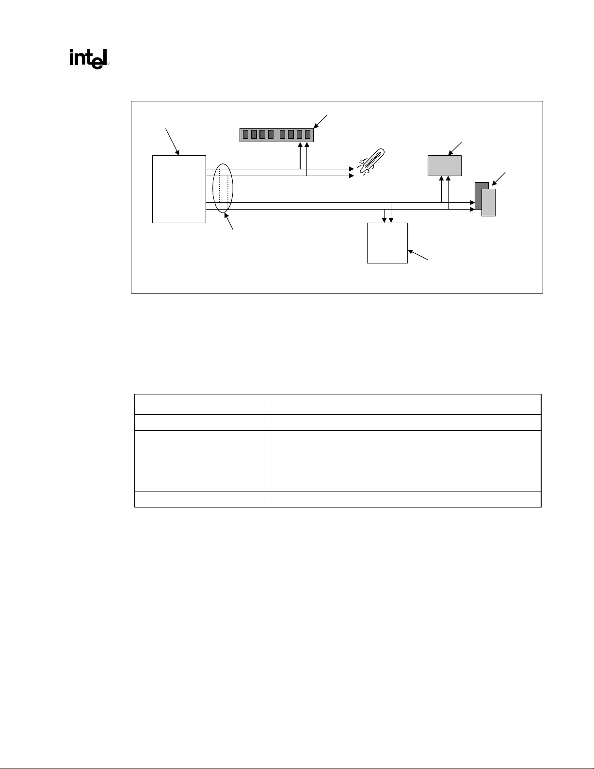
Intel® 820E Chipset
R
Figure 57. SMBUS/SMLink Interface
Host controller
slave interface
SMBus
82801BA
ICH2
SMLink
Wire OR
(optional)
SPD data
SMBCLK
SMBDATA
SMLink0
SMLink1
Temperature on
thermal sensor
®
Intel
8255
Network
interface
card on PCI
Microcontroller
Motherboard
LAN controller
smbus_smlink_IF
Note: Intel does not support external access to the ICH2’s integrated LAN controller via the SMLink interface.
Also, Intel does not support access to the ICH2’s SMBus slave interface by the ICH2’s SMBUS host
controller.
The following table describes the pull-up requirements for different implementations of the SMBus and
SMLink signals.
Table 20. Pull-Up Requirements for SMBus and SMLink Signals
SMBus / SMLink Use Implementation
Alert-on-LAN* signals 4.7 kΩ pull-up resistors to 3.3 VSB are required.
GPIOs Pull-up resistors to 3.3 VSB and the signals must be allowed.
To change states on power-up. (For example, during power-up the ICH2
will drive heartbeat messages until the BIOS programs these signals as
GPIOs.) The values of the pull-up resistors depend on the loading on the
GPIO signal.
Unused 4.7 kΩ pull-up resistors to 3.3 V
are required.
SB
Design Guide 95
Page 96

Intel® 820E Chipset
R
2.18. PCI
The ICH2 provides a PCI Bus interface that is compliant with the PCI Local Bus Specification, Revision
2.2. The implementation is optimized for high-performance data streaming when the ICH2 acts as either
the target or the initiator on the PCI bus. For more information on the PCI Bus interface, refer to the PCI
Local Bus Specification, Revision 2.2.
The ICH2 supports six PCI Bus masters, excluding the ICH2, by providing six REQ#/GNT# pairs. In
addition, the ICH2 supports two PC/PCI REQ#/GNT# pairs, one of which is multiplexed with a PCI
REQ#/GNT# pair.
Figure 58. PCI Bus Layout Example
ICH2
2.19. RTC
The ICH2 contains a real-time clock (RTC) with 256 bytes of battery-backed SRAM. The internal RTC
module provides two key functions: keeping the date and time and storing system data in its RAM when
the system is powered down.
This section will discuss the recommended hookup for the RTC circuit for the ICH2.
Note: This circuit is not the same as the circuit used for the PIIX4.
PCI_bus_layout_ex
96 Design Guide
Page 97

Intel® 820E Chipset
R
2.19.1. RTC Crystal
The ICH2 RTC module requires an external 32.768 kHz oscillating source connected on the RTCX1 and
RTCX2 pins. The following figure shows the external circuitry that comprises the oscillator of the ICH2
RTC.
Figure 59. External Circuitry for the ICH RTC
2
VCC3_3SBY
Vbat_rtc
1 k
Ω
Ω
1 k
0.047 uF
C1
1 µF
32768 Hz
Xtal
C2
R1
10 M
1
C3
1
R2
10 M
VCCRTC
RTCX2
Ω
RTCX1
Ω
VBIAS
VSS
rtc_cir
NOTES:
1. The exact capacitor value must be based on the crystal maker’s recommendation.
2. This circuit is not the same as the one used for PIIX4.
3. VCC
: Power for RTC well
RTC
4. RTCX2: Crystal input 2 – Connected to the 32.768 kHz crystal
5. RTCX1: Crystal input 1 – Connected to the 32.768 kHz crystal
6. VBIAS: RTC bias voltage – This pin is used to provide a reference voltage, and this DC voltage sets a current
that is mirrored throughout the oscillator and buffer circuitry.
: Ground
7. V
SS
3
4
5
6
7
2.19.2. External Capacitors
To maintain RTC accuracy, the external capacitor C1 must have a capacitance of 0.047 µF, and the
external capacitor values (C2 and C3) should be chosen to provide the manufacturer’s specified load
capacitance (C
used), and package. When the external capacitor values are combined with the capacitance of the trace,
socket, and package, the closer the capacitor value can be matched to the actual load capacitance of the
crystal used, the more accurate the RTC will be.
The following equation can be used to choose the external capacitance values (C2 and C3):
C
= (C2 × C3) / (C2 + C3) + C
LOAD
C3 can be chosen such that C3 > C2. Then C2 can be trimmed to obtain the 32.768 kHz.
Design Guide 97
) for the crystal, when combined with the parasitic capacitance of the trace, socket (if
LOAD
PARASITIC
.
Page 98

Intel® 820E Chipset
c
R
2.19.3. RTC Layout Considerations
• Minimize the RTC lead lengths. Approximately 0.25 inch is sufficient.
• Minimize the capacitance between Xin and Xout in the routing.
• Put a ground plane under the XTAL components.
• Do not route switching signals under the external components (unless on the other side of the
board).
• The oscillator V
should be clean. Use a filter (e.g., an RC low-pass) or a ferrite inductor.
CC
2.19.4. RTC External Battery Connection
The RTC requires an external battery connection to maintain its functionality and its RAM while the
ICH2 is not powered by the system.
Example batteries are the Duracell* 2032, 2025 or 2016 (or equivalent), which provide many years of
operation. Batteries are rated by storage capacity. The battery life can be calculated by dividing the
capacity by the average current required. For example, if the battery storage capacity is 170 mAh
(assumed usable) and the average current required is 3 µA, the battery life will be at least:
170,000 µAh / 3 µA = 56,666 h = 6.4 years
The battery voltage can affect the RTC accuracy. In general, when the battery voltage decays, the RTC
accuracy also decreases. High accuracy can be obtained when the RTC voltage is within the range 3.0 V
to 3.3 V.
The battery must be connected to the ICH2 via an isolation Schottky diode circuit. The Schottky diode
circuit allows the ICH2 RTC well to be powered by the battery when system power is unavailable, but by
system power when it is available. For this purpose, the diodes are set to be reverse-biased when system
power is unavailable. The following figure is an example diode circuit.
Figure 60. Diode Circuit Connecting RTC External Battery
VCC3_3SBY
1 k
Ω
VccRTC
1.0 µF
+
-
RTC_ext_batt_diode_cir
98 Design Guide
Page 99

Intel® 820E Chipset
R
A standby power supply should be used in a desktop system to provide continuous power to the RTC
when available, which will significantly increase the RTC battery life and thereby increase the RTC
accuracy.
2.19.5. RTC External RTCRST Circuit
The ICH2 RTC requires additional external circuitry. The RTCRST# signal is used to reset the RTC
well. The external capacitor and the external resistor between RTCRST# and the RTC battery (V
were selected to create an RC time delay, such that RTCRST# will go high some time after the battery
voltage becomes valid. The RC time delay should be within the range 10 ms–20 ms. When RTCRST# is
asserted, bit 2 (RTC_PWR_STS) in the GEN_PMCON_3 (General PM Configuration 3) register is set to
1 and remains set until cleared by software. As a result, when the system boots, the BIOS knows that the
RTC battery has been removed.
Figure 61. RTCRST External Circuit for ICH2 RTC
Diode/
Battery
Circuit
VCC3_3SBY
1 k
Ω
VccRTC
1.0 µF
BAT
)
Ω
8.2 k
RTCRST#
2.2 µF
RTCRST
Circuit
rtc_rtcrst_ich
This RTCRST# circuit is combined with the diode circuit (Figure 60. Diode Circuit Connecting RTC
External Battery), which allows the RTC well to be powered by the battery when system power is
unavailable. Figure 59 is an example of the circuit used in conjunction with the external diode circuit.
Design Guide 99
Page 100

Intel® 820E Chipset
R
2.19.6. RTC Routing Guidelines
• All RTC OSC signals (RTCX1, RTCX2, VBIAS) should be routed with trace lengths of less than 1
inch. The shorter, the better.
• Minimize the capacitance between RTCX1 and RTCX2 in the routing. (Optimally, there would be a
ground line between them.)
• Put a ground plane under all external RTC circuitry.
• Do not route any switching signals under the external components (unless on the other side of the
ground plane).
2.19.7. VBIAS DC Voltage and Noise Measurements
• The steady-state VBIAS is a DC voltage of approximately 0.38 V ± 0.06 V.
• When the battery is inserted, the VBIAS is “kicked” to approximately 0.7 V–1.0 V, but it will return
to its DC value within a few ms.
• Noise on VBIAS must be minimized at ≤200 mV.
• VBIAS is very sensitive and cannot be probed directly. It can be probed through a 0.01 µF
capacitor.
• Excess noise on VBIAS can cause the ICH2 internal oscillator to misbehave or even stop
completely.
• To minimize VBIAS noise, it is necessary to implement the routing guidelines described previously
and the required external RTC circuitry.
2.19.8. RTC-Well Input Strap Requirements
All RTC-well inputs (RSMRST#, RTCRST#, INTRUDER#) must be either pulled up to VCCRTC or
pulled down to ground while in G3 state. RTCRST# when configured as shown in Figure 61 meets this
requirement. RSMRST# should have a weak external pull-down to ground and INTRUDER# should
have a weak external pull-up to VCCRTC. This will prevent these nodes from floating in G3, and
correspondingly will prevent ICCRTC leakage that can cause excessive coin-cell drain. The PWROK
input signal should also be configured with an external weak pull-down.
2.20. SPKR Pin Consideration
The effective impedance of the speaker and codec circuitry on the SPKR signal line must be greater than
50 kΩ. Otherwise, the TCO Timer Reboot function will be disabled erroneously. SPKR is used both as
the output signal to the system speaker and as a functional strap. The strap function enables or disables
the “TCO Timer Reboot function,” depending on the state of the SPKR pin on the rising edge of
POWEROK. When enabled, the ICH2 sends an SMI# to the processor when a TCO timer timeout
occurs. The status of this strap is readable via the NO_REBOOT bit (bit 1, D31: F0, offset D4h). The
SPKR signal has a weak integrated pull-up resistor, which is enabled only during boot/reset. Therefore,
its default state when the pin is a “no connect” is a logical one or enabled. To disable this feature, a
jumper can be populated to pull the signal line low (see Figure 62). The value of the pull-down must be
such that the voltage divider caused by the pull-down and integrated pull-up resistors will be read as a
100 Design Guide
 Loading...