

Page 1
Intel® Celeron® Processor
up to 1.10 GHz
Datasheet
■ Available at 1.10 GHz, 1 GHz, 950 MHz,
900 MHz, 850 MHz, 800 MHz, 766 MHz,
733 MHz, 700 MHz, 667 MHz, 633 MHz,
600 MHz, 566 MHz, 533 MH z,
533A MHz, 500 MHz, 466 MHz,
433 MHz, 400 MHz, 366 MH z, 333 MHz,
and 300A MHz core frequencies with
128 KB level-two cache (on die); 300 MHz
and 266 MHz core frequencies without
level-two cache.
■ Intel’s latest Celeron
®
processors in the
FC-PGA/FC-PGA2 package are
manufactured using the advanced 0.18
micron technology.
■ Binary compatible with applications
running on previous members of the Intel
microprocessor line.
■ Dynamic execution microarchitecture.
■ Operates on a 100/66 MHz, transaction-
oriented system bus.
■ Specifically designed for uni-processor
based Value PC systems, with the
capabilities of MMX™ technology.
■ Power Management capabilities.
■ Optimized for 32-bit applications running
on advanced 32-bit operating systems.
■ Uses cost-effective packaging technology.
—Single Edge Processor (S.E.P.) Package
to maintain compatibility with SC242
(processor core frequencies (MHz):
266, 300, 300A, 333, 366, 400, 433).
—Plastic Pin Grid Array (PPGA) Package
(processor core frequencies (MHz):
300A, 333, 366, 400, 433, 466, 500,
533).
—Flip-Chip Pin Grid Array (FC-PGA /
FC-PGA2) Package (processor core
frequencies (MHz); 533A, 566, 600,
633, 667, 700, 733, 766, 800, 850, 900,
950); (GHz); 1, 1.10
■ Integrated high-performance 32 KB
instruction and data, nonblocking, levelone cache: separate 16 KB instruction and
16 KB data caches.
■ Integrated thermal diode.
The Intel® Celeron® processor is designed for uni-processor based Value PC desktops and is
binary compatible with previous generation Intel architecture pro cessors. The Celero n processor
provides good performance for applications running on advanced operating systems such as
Microsoft* Windows*98, Windows NT*, Windows* 2000, Windows XP* and Linux*. This is
achieved by integrating the best attributes of Intel processors—the dynamic execution
performance of the P6 microarchitecture plus the capabilities of MMX™ technology—bringing
a balanced level of performance to the Value PC market segment. The Celeron processor offers
the dependability you would expect from Intel at an exceptional value. Systems based on
Celeron processors also include the latest features to simplify s ystem managemen t and lower the
cost of ownership for small business and home environments.
PPGA Package
S.E.P. PackageFC-PGA2 Package FC-PGA Package
Document Number: 243658-020
January 2002
Page 2

Information in this document is provided in connection with Intel® products. No license, express or implied, by estoppel or otherwise, to any intellectual
property rights is granted by this document. Except as provided in Intel’s T erms and Conditions of Sale for such products, Intel assumes no liability
whatsoever, and Intel disclaims any express or implied warranty, relating to sale and/or use of Intel products including liability or warranties relating to
fitness for a particular purpose, merchantability, or infringement of any patent, copyright or other intellectual property right. Intel products are not
intended for use in medical, life saving, or life sustaining applications.
Intel may make changes to specifications and product descriptions at any time, without notice.
Designers must not rely on the absence or characteristics of any features or instructions marked "reserved" or "undefined." Intel reserves these for
future definition and shall have no responsibility whatsoever for conflicts or incompatibilities arising from future changes to the m.
®
The Intel
Celeron® processor may contain design defects or errors known as errata which may cause the product to deviate from published specifi-
cations. Current characterized errata are available on request.
Contact your local Intel sales office or your distributor to obtain the latest specifications and before placing your product order.
Copies of documents which have an ordering number and are referenced in this document, or other Intel literature, may be obtained by calling
1-800-548-4725 or by visiting Intel’s website at http://www.intel.com.
Intel, Celeron, Pentium, MMX and the Intel logo are trademarks or registered trademarks of Intel Corporation or its subsidiaries in the United States
and other countries.
*Other names and brands may be claimed as the property of others.
©
Copyright
1996–2002, Intel Corporation
Datasheet
Page 3

®
Intel
Celeron® Processor up to 1.10 GHz
Contents
1.0 Introduction.......................................................................................................................11
1.1 Terminology.........................................................................................................11
1.1.1 Package Terminology.............................................................................12
1.1.2 Processor Naming Convention...............................................................13
1.2 References..........................................................................................................14
2.0 Electrical Specifications....................................................................................................15
2.1 System Bus and Vref...........................................................................................15
2.2 Clock Control and Low Power States..................................................................15
2.2.1 Normal State—State 1 ...........................................................................16
2.2.2 AutoHALT Power Down State—State 2.................................................16
2.2.3 Stop-Grant State—State 3 .....................................................................17
2.2.4 HALT/Grant Snoop State—State 4 ........................................................17
2.2.5 Sleep State—State 5..............................................................................17
2.2.6 Deep Sleep State—State 6....................................................................18
2.2.7 Clock Control............... ....... ...... ...... ....... ...... ....... ...... ....... ...... ....... ...... ....18
2.3 Power and Ground Pins ......................................................................................18
2.3.1 Phase Lock Loop (PLL) Power...............................................................19
2.4 Processor Decoupling .........................................................................................19
2.4.1 System Bus AGTL+ Decoupling.............................................................19
2.5 Voltage Identification...........................................................................................20
2.6 System Bus Unused Pins....................................................................................21
2.7 Processor System Bus Signal Groups ................................................................21
2.7.1 Asynchronous Vs. Synchronous for System Bus Signals ......................23
2.7.2 System Bus Frequency Select Signal (BSEL[1:0]).................................23
2.8 Test Access Port (TAP) Connection....................................................................23
2.9 Maximum Ratings................................................................................................23
2.10 Processor DC Specifications...............................................................................24
2.11 AGTL+ System Bus Specifications .....................................................................33
2.12 System Bus AC Specifications............................................................................34
3.0 System Bus Signal Simulations........................................................................................52
3.1 System Bus Clock (BCLK) Signal Quality Specifications and
Measurement Guidelines ....................................................................................52
3.2 AGTL+ Signal Quality Specifications and Measurement Guidelines ..................55
3.3 Non-AGTL+ Signal Quality Specifications and Measurement Guidelines...........57
3.3.1 Overshoot/Undershoot Guidelines .........................................................57
3.3.2 Ringback Specification...........................................................................58
3.3.3 Settling Limit Guideline...........................................................................59
3.4 AGTL+ Signal Quality Specifications and Measurement Guidelines
(FC-PGA/FC-PGA2 Packages)...........................................................................59
3.4.1 Overshoot/Undershoot Guidelines (FC-PGA/FC-PGA2 Packages).......59
3.4.2 Overshoot/Undershoot Magnitude (FC-PGA/FC-PGA2 Packages).......59
3.4.3 Overshoot/Undershoot Pulse Duration (FC-PGA/FC-PGA2
Packages) ..............................................................................................60
3.4.4 Activity Factor (FC-PGA/FC-PGA2 Packages) ......................................60
Datasheet 3
Page 4

Intel® Celeron® Processor up to 1.10 GHz
3.4.5 Reading Overshoot/Undershoot Specification Tables
(FC-PGA/FC-PGA2 Packages)..............................................................61
3.4.6 Determining if a System meets the Overshoot/Undershoot
Specifications (FC-PGA/FC-PGA2 Packages).......................................62
3.5 Non-AGTL+ Signal Quality Specifications and Measurement Guidelines...........64
4.0 Thermal Specifications and Design Considerations.........................................................65
4.1 Thermal Specifications........................................................................................65
4.1.1 Thermal Diode........................................................................................68
5.0 Mechanical Specifications................................................................................................69
5.1 S.E.P. Package...................................................................................................69
5.1.1 Materials Information..............................................................................69
5.1.2 Signal Listing (S.E.P. Package) ............................................................70
5.2 PPGA Package ...................................................................................................79
5.2.1 PPGA Package Materials Information....................................................79
5.2.2 PPGA Package Signal Listing................................................................81
5.3 FC-PGA/FC-PGA2 Packages .............................................................................92
5.3.1 FC-PGA Mechanical Specifications .......................................................92
5.3.2 Mechanical Specifications (FC-PGA2 Package)....................................94
5.3.2.1 Recommended Mechanical Keep-Out Zones
(FC-PGA2 Package) .................................................................96
5.3.3 FC-PGA/FC-PGA2 Package Signal List.................................................97
5.4 Processor Markings (PPGA/FC-PGA/FC-PG A2 Packag es) .............................108
5.5 Heatsink Volumetric Keepout Zone Guide li nes.................. ...... ....... ...... ....... .....1 09
6.0 Boxed Processor Specifications.....................................................................................110
6.1 Mechanical Specifications for the Boxed Intel
®
Celeron® Processor................110
6.1.1 Mechanical Specifications for the S.E.P. Package...............................110
6.1.1.1 Boxed Processor Heatsink Weight..........................................112
6.1.1.2 Boxed Processor Retention Mechanism.................................112
6.1.2 Mechanical Specifications for the PPGA Package...............................113
6.1.2.1 Boxed Processor Heatsink Weight..........................................114
6.1.3 Mechanical Specifications for the FC-PGA/FC-PGA2 Packages.........114
6.1.3.1 Boxed Processor Heatsink Weight..........................................115
6.2 Thermal Specifications......................................................................................115
6.2.1 Thermal Requirements for the Boxed Intel
®
Celeron® Processor ... .....1 15
6.2.1.1 Boxed Processor Cooling Requirements ................................115
6.2.1.2 Boxed Processor Thermal Cooling Solution Clip ....................117
6.3 Electrical Requirements for the Boxed Intel
®
Celeron® Processor ...................117
6.3.1 Electrical Requirements .......................................................................117
7.0 Processor Signal Descript ion............................................. ...... ....... ...............................120
7.1 Signal Summaries.............................................................................................126
4 Datasheet
Page 5

Figures
®
Intel
Celeron® Processor up to 1.10 GHz
1 Clock Control State Machine...............................................................................16
2 BCLK to Core Logic Offset..................................................................................48
3 BCLK*, PICCLK, and TCK Generic Clock Waveform .........................................49
4 System Bus Valid Delay Timings ........................................................................49
5 System Bus Setup and Hold Timings..................................................................49
6 System Bus Reset and Configuration Timings (For the S.E.P. and
PPGA Packages) ................................................................................................50
7 System Bus Reset and Configuration Timings (For the
FC-PGA/FC-PGA2 Package)..............................................................................50
8 Power-On Reset and Configuration Timings.......................................................51
9 Test Timings (TAP Connection) ..........................................................................51
10 Test Reset Timings .............................................................................................51
11 BCLK, TCK, PICCLK Generic Clock Waveform at the Processor Core Pins .....53
12 BCLK, TCK, PICCLK Generic Clock Waveform at the Processor
Edge Fingers.......................................................................................................54
13 Low to High AGTL+ Receiver Ringback Tolerance.............................................56
14 Non-AGTL+ Overshoot/Undershoot, Settling Limit, and Ringback .....................57
15 Maximum Acceptable AGTL+ Overshoot/Undershoot Waveform
(FC-PGA/FC-PGA2 Packages)...........................................................................63
16 Non-AGTL+ Overshoot/Undershoot, Settling Limit, and Ringback ....................64
17 Processor Functional Die Layout (CPUID 0686h)...............................................67
18 Processor Functional Die Layout (up to CPUID 0683h)......................................67
19 Processor Substrate Dimensions (S.E.P. Package) ...........................................70
20 Processor Substrate Primary/Secondary Side Dimensions (S.E.P. Package)....70
21 Package Dimensions (PPGA Package) ..............................................................79
22 PPGA Package (Pin Side View)..........................................................................81
23 Package Dimensions (FC-PGA Package)...........................................................92
24 Package Dimensions (FC-PGA2 Package).........................................................94
25 Volumetric Keep-Out...........................................................................................96
26 Component Keep-Out .........................................................................................96
27 Package Dimensions (FC-PGA/FC-PGA2 Packages) ........................................97
28 Top Side Processor Markings (PPGA Package)...............................................108
29 Top Side Processor Markings (FC-PGA Package) ...........................................108
30 Top Side Processor Markings (FC-PGA2 Package) .........................................108
31 Retention Mechanism for the Boxed Intel® Celeron
®
Processor in the
S.E.P. Package .................................................................................................111
32 Side View Space Requirements for the Boxed Processor in the S.E.P.
Package ............................................................................................................111
33 Front View Space Requirements for the Boxed Processor in the S.E.P.
Package ............................................................................................................112
34 Boxed Intel
®
Celeron® Processor in the PPGA Package..................................113
35 Side View Space Requirements for the Boxed Processor in the PPGA
Package ............................................................................................................113
36 Conceptual Drawing of the Boxed Intel
®
Celeron® Processor in the
370-Pin Socket (FC-PGA/FC-PGA2 Packages)................................................114
37 Dimensions of Mechanical Step Feature in Heatsink Base for the
FC-PGA/FC-PGA2 Packages ...........................................................................114
38 Top View Airspace Requirements for the Boxed Processor in the
S.E.P. Package .................................................................................................115
Datasheet 5
Page 6

Intel® Celeron® Processor up to 1.10 GHz
39 Side View Airspace Requirements for the Boxed Intel® Celeron®
Processor in the FC-PGA/FC-PGA2 and PPGA Packages ..............................116
40 Volumetric Keepout Requirements for The Boxed Fan Heatsink......................116
41 Clip Keepout Requirements for the 370-Pin (Top View) ...................................117
42 Boxed Processor Fan Heatsink Power Cable Connector Description ..............118
43 Motherboard Power Header Placement for the S.E.P. Package ......................119
44 Motherboard Power Header Placement Relative to the 370-pin Socket...........119
6 Datasheet
Page 7

Tables
®
Intel
Celeron® Processor up to 1.10 GHz
1 Processor Identification.......................................................................................13
2 Voltage Identification Definition...........................................................................20
3Intel
®
Celeron® Processor System Bus Signal Groups.......................................22
4 Absolute Maximum Ratings..... ....... ...... ...... ....... ...... ....... ...... ....... ...... .................24
5 Voltage and Current Specifications.....................................................................25
6 AGTL+ Signal Groups DC Specifications............................................................31
7 Non-AGTL+ Signal Group DC Specifications......................................................32
8 Processor AGTL+ Bus Specifications .................................................................33
9 System Bus AC Specifications (Clock) at the Processor Edge Fingers
(for S.E.P. Package)............................................................................................35
10 System Bus AC Specifications (Clock) at the Processor
Core Pins (for Both S.E.P. and PGA Packages).................................................36
11 System Bus AC Specifications (SET Clock)........................................................37
12 Valid Intel
®
Celeron® Processor System Bus, Core Frequency..........................38
13 System Bus AC Specifications (AGTL+ Signal Group) at the Processor
Edge Fingers (for S.E.P. Package).....................................................................39
14 System Bus AC Specifications (AGTL+ Signal Group) at the Processor
Core Pins (for S.E.P. Package)...........................................................................39
15 Processor System Bus AC Specifications (AGTL+ Signal Group) at the
Processor Core Pins (for PPGA Package)..........................................................40
16 System Bus AC Specifications (AGTL+ Signal Group) at the Processor
Core Pins (for FC-PGA/FC-PGA2 Packages).....................................................40
17 System Bus AC Specifications (CMOS Signal Group) at the Processor
Edge Fingers (for S.E.P. Package).....................................................................41
18 System Bus AC Specifications (CMOS Signal Group) at the Processor
Core Pins (for Both S.E.P., PGA, and FC-PGA/FC-PGA2 Packages)................41
19 System Bus AC Specifications (CMOS Signal Group) .......................................42
20 System Bus AC Specifi cations (Reset Conditions)
(for Both S.E.P. and PPGA Packages) ...............................................................42
21 System Bus AC Specifications (Reset Conditions) (for the
FC-PGA/FC-PGA2 Packages) ............................................................................42
22 System Bus AC Specifications (APIC Clock and APIC I/O) at the
Processor Edge Fingers (for S.E.P. Package)....................................................43
23 System Bus AC Specifications (APIC Clock and APIC I/O) at the
Processor Core Pins (For S.E.P. and PGA Packages).......................................44
24 System Bus AC Specifications (APIC Clock and APIC I/O)................................45
25 System Bus AC Specifications (TAP Connection) at the Processor
Edge Fingers (For S.E.P. Package)....................................................................45
26 System Bus AC Specifications (TAP Connection) at the Processor
Core Pins (for Both S.E.P. and PPGA Packages)...............................................46
27 System Bus AC Specifications (TAP Connection) ..............................................47
28 BCLK Signal Quality Specifications for Simulation at the Processor Core
(for Both S.E.P. and PPGA Packages) ...............................................................52
29 BCLK/PICCLK Signal Quality Specifications for Simulation at the
Processor Pins (for the FC-PGA/FC-PGA2 Packages).......................................53
30 BCLK Signal Quality Guidelines for Edge Finger Measurement
(for the S.E.P. Package)......................................................................................54
31 AGTL+ Signal Groups Ringback Tolerance Specifications at the
Processor Core (For Both the S.E.P. and PPGA Packages)..............................55
Datasheet 7
Page 8

Intel® Celeron® Processor up to 1.10 GHz
32 AGTL+ Signal Groups Ringback Tolerance Specifications at the
Processor Pins (For FC-PGA/FC-PGA2 Package s) .......... ...... ....... ...... ....... ...... .55
33 AGTL+ Signal Groups Ringback Tolerance Guidelines for Edge Finger
Measurement on the S.E.P. Package.................................................................56
34 Signal Ringback Specifications for Non-AGTL+ Signal Simulation at the
Processor Core (S.E.P. and PPGA Packages)...................................................58
35 Signal Ringback Guidelines for Non-AGTL+ Signal Edge Finger
Measurement (S.E.P. Package)..........................................................................58
36 Signal Ringback Specifications for Non-AGTL+ Signal Simulation at the
Processor Pins (FC-PGA/FC-PGA2 Packages)..................................................58
37 Example Platform Information............................... ...... ....... ...... ....... ...... ....... ...... .61
38 66 MHz AGTL+ Signal Group Overshoot/Undershoot Tolerance at
Processor Pins (FC-PGA/FC-PGA2 Packages)..................................................62
39 33 MHz CMOS Signal Group Overshoot/Undershoot Tolerance at
Processor Pins (FC-PGA/FC-PGA2 Packages)..................................................63
40 Processor Power for the PPGA and FC-PGA Packages ....................................66
41 Intel
®
Celeron® Processor for the FC-PGA2 Package Thermal Design Power .67
42 Thermal Diode Parameters (S.E.P. and PPGA Packages).................................68
43 Thermal Diode Parameters (FC-PGA/FC-PGA2 Packages)...............................68
44 Thermal Diode Interface......................................................................................68
45 S.E.P. Package Signal Listing by Pin Number....................................................71
46 S.E.P. Package Signal Listing by Signal Name ..................................................75
47 Package Dimensions (PPGA Package)..............................................................80
48 Information Summary (PPGA Package) .............................................................80
49 PPGA Package Signal Listing by Pin Number ....................................................82
50 PPGA Package Signal Listing in Order by Signal Name ....................................87
51 Package Dimensions (FC-PGA Package) ..........................................................93
52 Processor Die Loading Parameters (FC-PGA Package) ....................................93
53 Package Dimensions (FC-PGA2 Package) ........................................................95
54 Processor Case Loading Parameters (FC-PGA2 Package) ...............................95
55 FC-PGA/FC-PGA2 Signal Listing in Order by Signal Name ...............................98
56 FC-PGA/FC-PGA2 Signal Listing in Order by Pin Number...............................103
57 Boxed Processor Fan Heatsink Spatial Dimensions for the S.E.P. Package ...112
58 Fan Heatsink Power and Signal Specifications.................................................118
59 Alphabetical Signal Reference..........................................................................120
60 Output Signals...................................................................................................126
61 Input Signals .....................................................................................................127
62 Input/Output Signals (Single Driver)..................................................................128
63 Input/Output Signals (Multiple Driver) ...............................................................128
8 Datasheet
Page 9
Revision History
Revision Date Description
-020 January 2002
®
Intel
Celeron® Processor up to 1.10 GHz
• Added IHS specifications for 900 MHz, 950 MHz, and 1 GHz.
• Added 566 MHz specification for CPUID of 068Ah.
Datasheet 9
Page 10

Intel® Celeron® Processor up to 1.10 GHz
This page is intentionally left blank.
10 Datasheet
Page 11

1.0 Introduction
®
Intel
Celeron® Processor up to 1.10 GHz
The Intel® Celeron® processor is based on the P6 microarchitecture and is optimized for the Value
PC market segment. The Intel Celeron processor, like the Pentium
Dynamic Execution microarchitecture and executes MMX™ technology instructions for enhanced
media and communication performance. The Intel Celeron processor also utilizes multiple lowpower states such as AutoHALT, S t o p-Grant , Sleep, and Deep Sleep to con serv e p ower dur ing idle
times.
The Intel Celeron processor is capabl e of running today ’ s mos t common PC appli cations with up to
4 GB of cacheable memory space. As this processor is intended for Value PC systems, it does not
provide multiprocessor support. The Pentium II and Pentium
multiprocessor system designs.
To be cost-effective at both the processor and system level, the Intel Celeron processor utilizes
cost-effective packaging technologies. They are the S.E.P. (Single-Edge Processor) package, the
PPGA (Plastic Pin Grid Array) package, the FC-PGA (Flip-Chip Pin Grid Array) package, and the
FC-PGA2 (Flip-Chip Pin Grid Array) package. Refer to the Intel
Specification Update for the latest packaging and frequency support information (Order Number
243337).
Note: This datasheet describes the Intel Celeron processor for the PPGA package, FC-PGA/FC-PGA2
packages, and the S.E.P. Package versions. Unless otherwise specified, the information in this
document applies to all versions and information on PGA packages, refer to both PPGA and
FC-PGA packages.
1.1 Terminology
®
II processor, features a
®
III processors should be used for
®
Celeron® Processor
In this document, a ‘#’ symbol after a signal name refers to an active low signal. This means that a
signal is in the active state (based on the name of the signal) when driven to a low level. For
example, when FLUSH# is low, a flush has been requested. When NMI is high, a nonmaskable
interrupt has occurred. In the case of signals where the name does not imply an active state but
describes part of a binary seq uence (such as address or data), the ‘#’ symbol implies that the signal
is inverted. For example, D[3:0] = ‘HLHL’ refers to a hex ‘A ’, and D[3:0]# = ‘LHLH’ also refers to
a hex ‘A’ (H= High logic level, L= Low logic level).
The term “system bus” refers to the interface between the processor, system core logic (a.k.a. the
AGPset components), and other bus agents. The system bus is an interface to the processor,
memory, and I/O.
Datasheet 11
Page 12

®
Intel
Celeron® Processor up to 1.10 GHz
1.1.1 Package Terminology
The following terms are used often in this document and are explained here for clarification:
• Processor substrate—The structure on which passive components (resistors and capacitors)
are mounted.
• Processor core—The processor’s execution engine.
• S.E.P. Package—Single-Edge Processor Package, which consists of a processor substrate,
processor core, and passive compone nts. This package d iffers f rom the S.E.C. C artridge as this
processor has no external plastic cover, thermal plate, or latch arms.
• PPGA package—Plastic Pin Grid Array package. The package is a pinned laminated printed
circuit board structure.
• FC-PGA — Flip-Chip Pin Grid Array. The FC-PGA uses the same 370-pin zero insertion
force socket (PGA370) as the PPGA. Thermal solutions are attached directly to the back of the
processor core package without the use of a thermal plate or heat spreader.
• FC-PGA2 — Flip Chip Pin Gr id Array 2. The FC-P G2A uses t he same 370 -pin zero inser tion
force socket (PGA370) as the PPGA. The FC-PGA2 package contains an Integrated Heat
Spreader that covers the processor die.
• Keepout zone - The area on or near a FC-PGA/FC-PGA2 packaged processor that system
designs can not utilize.
• Keep-in zone - The area of a FC-PGA packaged processor that thermal solutions may utilize.
Additional terms referred to in this and other related documentation:
• SC242—242-contact slot connector. A processor in the S.E.P. Package uses this connector to
interface with a system board.
• 370-pin socket (PGA370)—The zero insertion force (ZIF) socket in which a processor in the
PPGA package will use to interface with a system board.
• Retention mechanism—A mechanical assembly which holds the package in the SC242
connector.
12 Datasheet
Page 13
1.1.2 Processor Naming Convention
A letter(s) is added to certain processo rs (e.g ., 5 33 A MHz) when the core frequency alone may not
uniquely identify the processor. Below is a summary of what each letter means as well as a table
listing all the FC-PGA/FC-PGA2 processors for the PGA370 socket.
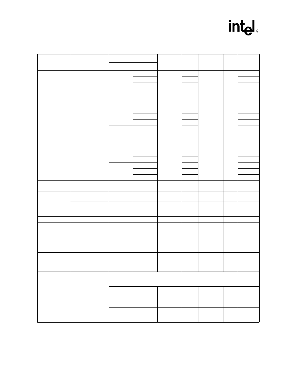
T able 1. Processor Identification
®
Intel
Celeron® Processor up to 1.10 GHz
Processor Core Frequency
300 MHz 300 MHz 66 065xh
300A MHz 300 MHz 66 066xh
366 MHz 366 MHz 66 066xh
400 MHz 400 MHz 66 066xh
433 MHz 433 MHz 66 066xh
466 MHz 466 MHz 66 066xh
500 MHz 500 MHz 66 066xh
533 MHz 533 MHz 66 066xh
533A MHz 533 MHz 66 068xh
566 MHz 566 MHz 66 068xh
600 MHz 600 MHz 66 068xh
633 MHz 633 MHz 66 068xh
667 MHz 667 MHz 66 068xh
700 MHz 700 MHz 66 068xh
733 MHz 733 MHz 66 068xh
766 MHz 766 MHz 66 068xh
800 MHz 800 MHz 100 068xh
850 MHz 850 MHz 100 068xh
900 MHz 900 MHz 100 068xh
950 MHz 950 MHz 100 068xh
1 GHz 1 GHz 100 068xh
1.10 GHz 1.10 MHz 100 068xh
System Bus Frequency
(MHz)
CPUID
1
NOTES:
1. Refer to the Intel
®
Celeron® Processor Specification Update for the exact CPUID for each processor.
Datasheet 13
Page 14

®
Intel
Celeron® Processor up to 1.10 GHz
1.2 References
The reader of this specification should also be familiar with material and concepts presented in the
following documents:
• AP-485, Intel
• AP-589, Design for EMI (Order Number 243334)
• AP-900, Identifying Support for Streaming SIMD Extensions in the Processor and Operating
• AP-905, Pentium
• AP-907, Pentium
• Intel
• Intel
• Intel
• Intel
• 370-Pin Socket (PGA370) Design Guidelines (Order Number 244410)
• Intel
1
System
®
Pentium® III Processor for the PGA370 Socket at 500 MHz to 933 MHz Datasheet
(Order Number 245264)
®
Pentium® III Processor Thermal Metrology for CPUID 068h Family
®
Pentium® III Processor Software Application Development Application Notes
®
Celeron® Processor Specification Update (Order Number 243748)
®
Architecture Software Developer's Manual (Order Number 243193)
®
Processor Identification and the CPUID Instruction (Order Number 241618)
1
®
III Processor Thermal Design Guidelines
®
III Processor Power Distribution Guidelines
1
1
1
1
1
— Volume I: Basic Architecture (Order Number 243190)
— Volume II: Instruction S et Ref erence (Order Number 243191)
— Volume III: System Programming Guide (Order Number 243192)
®
• Intel
• Intel
440EX AGPset Design Guide (Order Number 290637)
®
Celeron® Processor with the Intel® 440LX AGPset Design Guide
(Order Number 245088)
®
• Intel
• Intel
440BX AGPset Design Guide (Order Number 290634)
®
Celeron® Processor with the Intel® 440ZX-66 AGPset Design Guide
(Order Number 245126)
®
• Intel
Celeron® Processor (PPGA) at 466 MHz Thermal Solutions Guidelines
(Order Number 245156)
Notes:
1. This reference material can be found on the Intel Developer’s Web site located at
http://developer.intel.com.
2. For a complete listing of the Intel
®
Celeron® processor reference material, refer to the Intel
Developer’s Web site when this processor is formally launched. The Web site is located at
http://developer.intel.com/design/celeron/.
14 Datasheet
Page 15

2.0 Electrical Specifications
2.1 System Bus and VREF
®
Intel
Celeron® Processor up to 1.10 GHz
Celeron processor signals use a variation of the low voltage Gunning Transceiver Logic (GTL)
signaling technology. The Intel
Celeron processor system bus specification is similar to the GTL
specification, but has been enhanced to provide larger noise margins and reduced ringing. The
improvements are accomplished by increasing the termination voltage level and controlling the
edge rates. Because this specification is dif ferent f rom the stand ard GTL specification, it is referred
to as Assisted Gunning Transceiver Logic (AGTL+) in this document.
The Celeron processor varies from the Pentium Pro processor in its output buffer implementation.
The buffers that drive the system bus signals on the Celeron processor are actively driven to
V
CC
for one clock cycle during the low-to-high transition. This improves rise times and
CORE
reduces overshoot. These signals should still be considered open-drain and require termination to a
supply that provides the logic-high signal level.
The AGTL+ inputs use differential receivers which require a reference signal ( V
REF). VREF is used
by the receivers to determine if a signal is a logic-high or a logic-low, and is provided to the
processor core by either the processor substrate (S.E.P. Package) or the motherboard (PGA370
socket). Local V
REF copies should be generate d on the motherboard for all other devices on the
AGTL+ system bus.
Termination is used to pull the bus up to the high voltage level and to control reflections on the
transmission line. The processor may contain termination resistors (S.E.P. Package, FC-PGA
Package, and FC-PGA2 Package) that provide termination for one end of the Intel Celeron
processor system bus. Otherwise, this termination must exist on the motherboard.
Solutions exist for single-ended termination as well, though this implementation changes system
design and eliminate backwards compatibility for Celeron processors in the PPGA package.
Single-ended termination designs must still provide an AGTL+ termination resistor on the
motherboard for the RESET# signal.
The AGTL+ bus depends on incident wave switching. Therefore timing calculations for AGTL+
signals are based on motherboard flight time as opposed to capacitive deratings. Analog signal
simulation of the Intel Celeron processor system bus, including trace lengths, is highly
recommended when designing a system. See the Pentium
and the Pentium
®
II Processor I/O Buffer Models, Quad Format (Electronic Form) for details.
®
II Processor AG TL+ Layout Guidelines
2.2 Clock Control and Low Power St ates
Celeron processors allow the use of AutoHALT, Stop-Grant, Sleep, and Deep Sleep states to reduce
power consumption by stopping the clock to internal sections of the processor, depending on each
particular state. See Figure 1 for a visual representation of the Intel Celeron processor low power
states.
For the processor to fully realize the low current consumption of the Stop-Grant, Sleep, and Deep
Sleep states, a Model Specific Register (MSR) bit must be set. For the MSR at 02Ah (hex), bit 26
must be set to a ‘1’ (this is the power on default setting) for the processor to stop all internal clocks
during these modes. For more information, see the Pentium
(Order Number 243502).
Datasheet 15
®
II Processor Developer's Manual
Page 16
®
Intel
Celeron® Processor up to 1.10 GHz
2.2.1 Normal State—State 1
This is the normal operating state for the processor.
2.2.2 Aut oHALT Power Down State—State 2
AutoHALT is a low power state entered when the processor executes the HALT instruction. The
processor will transition to the Normal state upon the occurrence of SMI#, BINIT#, INIT#, or
LINT[1:0] (NMI, INTR). RESET# will cause the processor to immediately initialize itself.
The return from a System Management Interrupt (SMI) handler can be to either Normal Mode or
the AutoHALT Power Down state. See the Intel Architecture Software Developer's Manual,
Volume III: System Programmer's Guide (Order Number 243192) for more information.
FLUSH# will be serviced during the AutoHALT state, and the processor will return to the
AutoHALT state.
The system can generate a STPCLK# while the processor is in the AutoHALT Power Down state.
When the system deasserts the STPCLK# interrupt, the processor will return execution to the
HALT state.
Figure 1. Clock Control State Machine
2. Auto HALT Power Down State
BCLK running.
Snoops and interrupts allowed.
Snoop
Event
Occurs
4. Auto HALT Power Down State
BCLK running.
Snoops and interrupts allowed.
Snoop
Event
Serviced
HALT Instruction and
HALT Bus Cycle generated
INIT#, BINIT#, INTR, SMI#,
RESET#
STPCLK# Deasserted
and Stop Grant entered
from Auto HALT.
Snoop event occurs
Snoop event serviced
1. Normal State
Normal execution.
STPCLK#
asserted
3. Stop Grant State
BCLK running.
Snoops and interrupts allowed.
SLP#
asserted
5. Sleep State
BCLK running.
Snoops and interrupts allowed.
BCLK
input
stopped
STPCLK#
deasserted
SLP#
deasserted
BCLK
input
restarted
6. Deep Sleep State
BCLK stopped.
No Snoops and interrupts allowed.
16 Datasheet
Page 17

2.2.3 Stop-Grant State—State 3
The Stop-Grant state on the processor is entered when the STPCLK# signal is asserted.
Since the AGTL+ signal pins receive power from the system bus, these pins should not be driven
(allowing the level to return to V
state. In addition, all other input pins on the system bus should be driven to the inactive state.
BINIT# will not be serviced while the processor is in Stop-Grant state. The event will be latched
and can be serviced by software upon exit from Stop-Grant state.
FLUSH# will not be serviced during Stop-Grant state.
RESET# will cause the processor to immediately initialize itself, but the processor will stay in
Stop-Grant state. A transition back to the Normal state will occur with the deassertion of the
STPCLK# signal.
A transition to the HALT/Grant Snoop state will occur when the processor detects a snoop on the
system bus (see Section 2.2.4). A transition to the Sleep state (see Section 2.2.5) will occur with the
assertion of the SLP# signal.
While in the Stop-Grant State, SMI#, INIT#, and LINT[1:0] will be latched by the processor, and
only serviced when the processor returns to the Normal State. Only one occurrence of each event
will be recognized upon return to the Normal state.
TT) for minimum power drawn by t he te rm inat i on res ist o rs in th i s
®
Intel
Celeron® Processor up to 1.10 GHz
2.2.4 HALT/Grant Snoop State—State 4
The processor will respond to snoop transactions on the Celeron processor system bus while in
Stop-Grant state or in AutoHALT Power Down state. During a snoop transaction, the processor
enters the HAL T/Gran t Snoop state. The processor will stay in this state until the snoop on the Intel
Celeron processor system bus has been serviced (whether by the processor or another agent on the
Intel Celeron processor system bus). After the snoop is serviced, the processor will return to the
Stop-Grant state or AutoHALT Power Down state, as appropriate.
2.2.5 Sleep State—State 5
The Sleep state is a very low power state in which the processor maintains its context, maintains
the phase-locked loop (PLL), and has stopped all internal clocks. The Sleep state can only be
entered from Stop-Grant state. Once in the Stop-Grant state, the SLP# pin can be asserted, causing
the processor to enter the Sleep state. The SLP# pin is not recognized in the Normal o r AutoHALT
states.
Snoop events that occur while in Sleep State or during a transition into or out of Sleep state will
cause unpredictable behavior.
In the Sleep state, the processor is incapable of responding to snoop transactions or latching
interrupt signals. No transitions or assertions of signals (with the exception of SLP# or RESET#)
are allowed on the system bus while the processor is in Sleep state. Any transition on an input
signal before the processor has returned to Stop-Grant state will result in unpredictable behavior.
If RESET# is driven active while the processor is in the Sleep state, and held active as specified in
the RESET# pin specification, then the processor will reset itself, ignoring the transition through
Stop-Grant State. If RESET# is driven active while the processor is in the Sleep State, the SLP#
and STPCLK# signals should be deasserted immediately after RESET# is asserted to ensure the
processor correctly executes the Reset sequence.
Datasheet 17
Page 18

®
Intel
Celeron® Processor up to 1.10 GHz
While in the Sleep state, the processor is capable of entering its lowest power state, the Deep Sleep
state, by stopping the BCLK input. (See Section 2.2.6.) Once in the Sleep state, the SLP# pin can
be deasserted if another asynchronous system bus event occurs. The SLP# pin has a minimum
assertion of one BCLK period.
2.2.6 Deep Sleep State—State 6
The Deep Sleep state is the lowest power state the processor can enter while maintaining context.
The Deep Sleep state is entered by stopping the BCLK input (after the Sleep state was entered from
the assertion of the SLP# pin). The processor is in Deep Sleep state immediately after BLCK is
stopped. It is recommended that the BLCK input b e held low durin g the Deep Sleep S tate. Stop ping
of the BCLK input lowers the overall current consumption to leakage levels.
To re-enter the Sleep state, the BCLK input must be restarted. A period of 1 ms (to allow for PLL
stabilization) must occur before the processor can be considered to be in the Sleep State. Once in
the Sleep state, the SLP# pin can be deasserted to re-enter the Stop-Grant state.
While in Deep Sleep state, the processor is incapable of responding to snoop transactions or
latching interrupt signals. No transitions or assertions of signals are allowed on the system bus
while the processor is in Deep Sleep state. Any transition on an input signal before the processor
has returned to Stop-Grant state will result in unpredictable behavior.
2.2.7 Clock Control
BCLK provides the clock signal for the processor and on die L2 cache. During AutoHALT Power
Down and Stop-Grant states, the processor processes a system bus snoop. The processor does not
stop the clock to the L2 cache during AutoHALT Power Down or Stop-Grant states. Entrance into
the Halt/Grant Snoop state allows the L2 cache to be snooped, similar to the Normal state.
When the processor is in the Sleep or Deep Sleep states, it does not respond to interrupts or snoop
transactions. During the Sleep state, the internal clock to the L2 cache is not stopped. During the
Deep Sleep state, the internal clock to the L2 cache is stopped. The internal clock to the L2 cache
will be restarted only after the internal clocking mechanism for the processor is stable (i.e., the
processor has re-entered Sleep state).
PICCLK should not be removed during the AutoHALT Power Down or Stop-Grant states.
PICCLK can be removed during the Sleep or Deep Sleep states. When transitioning from the Deep
Sleep state to the Sleep state, PICCLK must be restarted with BCLK.
2.3 Power and Ground Pins
There are five pins defined on the S.E.P. Package for voltage identification (VID) and four pins on
the PPGA, FC-PGA, and FC-PGA2 packages. These pins specify the voltage required by the
processor core. These have been added to cleanly support voltage specification variations on
current and future Celeron processors.
For clean on-chip power distribution, Intel Celeron processors in the S.E.P. Package have 27 V
(power) and 30 V
voltage levels to the components. V
pins, while 4 V
For only the S.E.P. Package, one V
CC
V
must remain electrically separated from each other.
CORE
SS (ground) inputs. The 27 VCC pins are further divided to provide the different
CC
TT inputs (1.5 V) are used to provide a AGTL+ termination voltage to the processor .
CC
5
inputs for the processor core account for 19 of the VCC
CORE
pin is provided for Voltage Transient Tools. VCC5 and
CC
18 Datasheet
Page 19

®
Intel
Celeron® Processor up to 1.10 GHz
The PPGA package has more power (88) and ground (80) pins than the S.E.P. Package. Of the
power pins, 77 are used for the processor core (V
voltage (V
REF). The other 3 power pins are VCC
CC
1.5
) and 8 are used as a AGTL+ reference
CORE
, VCC
and VCC
2.5
and are used for future
CMOS
processor compatibility.
FC-PGA/FC-PGA2 packages have 77 V
V
CC
, and one VCC
2.5
cache. The V
The V
CC
CMOS
a design, the V
REF inputs are used as the AGTL+ reference voltage for the processor.
pin is provided as a feature for future processor support in a flexible design. In such
CC
CMOS
. VCC
CMOS
CORE
pin is used to provide the CMOS voltage for use by the platform.
CC
inputs supply the processor core, including the on-die L2
Additionally, 2.5 V must be provided to the V
input. The processor routes the CMOS voltage level through the package that it is compatible with.
For example, processors requiring 1.5 V CMO S vol ta ge level s rou t e 1.5 V to t he V
Each power signal, regardless of package, must meet the specifications stated in Table 4. In
addition, all V
CC
pins must be connected to a voltage island while all VSS pins have to
CORE
connect to a system ground plane. In addition, the motherboard must implement the V
voltage island or large trace. Similarly, all V
2.3.1 Phase Lock Loop (PLL) Power
It is highly critical that phase lock loop power delivery to the processor meets Intel’s requirements.
A low pass filter is required for power delivery to pins PLL1 and PLL2. This serves as an isolated,
decoupled power source for the internal PLL.
2.4 Processor Decoupling
Due to the large number of transistors and high internal clock speeds, the processor is capable of
generating large average current swings between low and f ull power states. This causes voltages on
power planes to sag below their nominal values if bulk decoupling is not adequate. Care must be
taken in the board design to ensure that the voltage provided to the processor remains within the
specifications listed in Table 5. Failure to do so can result in timing violations or a reduced lifetime
of the component.
, 77 ground pins, eight VREF, one VCC
CORE
CC
input and 1.5 V must be pr ovi ded to t he Vcc
2.5
SS pins must be connected to a system ground plane.
, one
1.5
CC
CMOS
TT pins as a
output.
1.5
2.4.1 System Bus AGTL+ Decoupling
The S.E.P. Package and FC-PGA/FC-PGA2 packages contain high frequency decoupling
capacitance on the processor substrate, where the PPGA package does not. Therefore, Celeron
processors in the PGA packages require high frequency decoupling on the system motherboard.
Bulk decoupling must be provided on the motherboard for proper AGTL+ bus operation for all
packages. See AP-585, Pentium
587, Pentium
Pentium
®
II Processor Power Distribution Guidelines (Order Number 243332), and the
®
II Processor Developer's Manual (Order Number 243502) for more information.
Datasheet 19
®
II Processor AGTL+ Guidelines (Order Number 243330), AP-
Page 20
®
Intel
Celeron® Processor up to 1.10 GHz
2.5 Voltage Identi fication
The processor’s voltage identification (VID) pins can be used to automatically select the VCC
voltage from a compatible voltage regulator. There are five VID pins (VID[4:0]) on the S.E.P.
Package, while there are only four (VID[3:0]) on the PGA packages. This is because there are no
Celeron processors in the PGA package that require more than 2.05 V (see Table 2).
VID pins are not signals, but rather are an open or short circuit to V
combination of opens and shorts defines the processor core’s required voltage. The VID pins also
allow for compatibility with current and future Intel Celeron processors.
Note that the ‘11 11 1’ (all opens) ID can be used to detect the abs ence of a pr ocessor cor e in a given
slot (S.E.P. Package only), as long as the power supply used does not affect the VID signals.
Detection logic and pull-ups should not affect VID inputs at the power source (see Section 7.0).
External logic monitoring the VID signals or the voltage regulator may require the VID pins to be
pulled-up. If this is the case, the VID pins should be pulled up to a TTL-compatible level with
external resistors to the power source of the regulator.
The power source chosen must be guaranteed to be stable whenever the voltage regulator’s supply
is stable. This will prevent the possibility of the processor supply going above the specified
V
CC
in the event of a failure in the supply for the VID lines. In the case of a DC-to-DC
CORE
converter, this can be accomplished by using the input voltage to the converter for the VID line
pull-ups. In addition, the power supply must supply the requested voltage or disable itself.
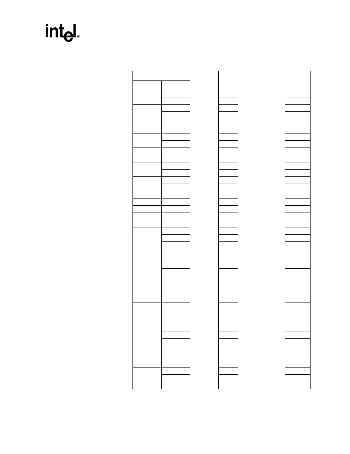
T a ble 2. Voltage Identification Definition
VID4
(S.E.P.P. only)
011111.30
011101.35
011011.40
011001.45
010111.50
010101.55
010011.60
010001.65
001111.70
001101.75
001011.80
001001.85
000111.90
000101.95
000012.00
000002.05
11111No Core
11110 2.1
VID3 VID2 V ID1 VID0 V
SS on the processor. The
CC
CORE
4
CORE
4
NOTES:
1. 0 = Processor pin connected to V
2. 1 = Open on processor; may be pulled up to TTL V
3. The Celeron proces sor core uses a 2.0 V power source.
4. VID 4 applies only to the S.E.P. Package. VID[3:0] applies to both S.E.P. and PGA packages.
SS.
on motherboard.
IH
20 Datasheet
Page 21

2.6 System Bus Unused Pins
®
Intel
Celeron® Processor up to 1.10 GHz
All RESERVED pins must remain unconnected. Connection of these pins to VCC
CORE
, VSS, or to
any other signal (including each other) can result in component malfunction or incompatibility
with future Celeron processor products. See Section 5.0 for a pin listing of the processor and the
location of each RESERVED pin.
For Intel Celeron processors in the S.E.P. Package, the TESTHI pin must be at a logic-high level
when the core power supply comes up. For more information, please refer to erratum C26 of the
®
Intel
Celeron® Processor Specification Update (Order Number 243748). Also note that the
TESTHI signal is not available on Intel Celeron processors in the PGA package.
PICCLK must be driven with a valid clock input and the PICD[1:0] lines must be pulled-up to
2.5 V even when the APIC will not be used. A separate pull-up resistor must be provided for each
PICD line.
For reliable operation, always connect unused inputs or bi-directional signals to their deasserted
signal level. The pull-up or pul l-down res i stor value is system dependent and should be c hosen
such that the logic-high (V
) and logic-low (VIL) requirements are met.
IH
For the S.E.P. Package, unused AGTL+ inputs should not be connected as the package substrate has
termination resistors. On the other hand, the PGA packages do not have AGTL+ termination in
their package and must have any unused AGTL+ inputs terminated through a pull-up resistor. For
designs that intend to only support the FC-PGA/FC-PGA2 processors, unused AGTL+ inputs will
be terminated by the processor’s on-die termination resistors and, thus, do not need to be
terminated on the motherboard. However, the reset pin should always be terminated on the
motherboard.
For unused CMOS inputs, active-low signals should be connected through a pull-up resistor to
meet V
meet V
requirements and active-high signals should be con nected through a pull-down res istor to
IH
requirements. Unused CMOS outputs can be left unconnected. A resistor must be used
IL
when tying bi-directional signals to power or ground. For any signal pulled to either power or
ground, a resistor will allow for system testability.
2.7 Processor System Bus Signal Groups
To simplify the following discussion, the Celeron processor system bus signals have been
combined into groups by buffer type. All Celeron processor system bus outputs are open drain
and require a high-level source provided externally by the termination or pull-up resistor.
AGTL+ input signals have dif fe rential input buffers, which use V
output signals require termination to 1.5 V. In this document, the term "AGTL+ Input" refers to the
AGTL+ input group as well as the AGTL+ I/O group when receiving. Similarly, "AGTL+ Output"
refers to the AGTL+ output group as well as the AGTL+ I/O group when driving.
EMI pins (S.E.P. Package only) should be connected to motherboard ground and/or to chassis
ground through zero ohm (0 Ω) resistors. The zero ohm resistors should be placed in close
proximity to the SC242 conn ect or. The path to chassis ground should be short in l eng th and have a
low impedance.
The PWRGOOD, BCLK, and PICCLK inputs can each be driven from ground to 2.5 V. Other
CMOS inputs (A20M#, IGNNE#, INIT#, LINT0/INTR, LINT1/NMI, PREQ#, SMI, SLP#, and
STPCLK#) must be pulled up to V
CC
. In addition, the CMOS, APIC, and TAP outputs are
CMOS
Datasheet 21
REF as a reference signal. AGTL+
Page 22
®
Intel
Celeron® Processor up to 1.10 GHz
open drai n and should be pulled high to VCC
. This ensures not only correct operation for
CMOS
current Intel Celeron processors, but compatibility for future Intel Celeron processor products as
well.
The groups and the signals contained within each group are shown in Table 3. Refer to Section 7.0
for descriptions of these signals.
Table 3. Intel® Celeron® Processor System Bus Signal Groups
Group Name Signals
AGTL+ Input BPRI#, DEFER#, RESET#
AGTL+ Output PRDY#
AGTL+ I/O
CMOS Input
4
CMOS Input PWRGOOD
CMOS Output
System Bus Clock BCLK
APIC Clock PICCLK
APIC I/O
TAP Input
TAP Output
Power/Other
4
4
4
5
A[31:3]#, ADS#, BNR#, BP[3:2]#, BPM[1:0]#, BR0#
HITM#, LOCK#, REQ[4:0]#,
A20M#, FLUSH#, IGNNE#, INIT#, LINT0/INTR, LINT1/NMI, PREQ#, SMI#, SLP#2,
STPCLK#
1,9
4
FERR#, IERR#, THERMTRIP#
9
9
PICD[1:0]
TCK, TDI, TMS, TRST#
TDO
CPUPRES#7, EDGCTRL7, EMI6, PLL[2:1]7, SLOTOCC#6, THERMDP, THERMDN,
CC
V
1.5
VID[4:0]
7
7
, VCC
6
, VCC
2.5
, VREF[7:0]7, VSS, VTT14, RTTCTRL12, BSEL[1:0]10, SLEWCTRL
11
, RS[2:0]#, TRDY#
3
5
6
, VCC
L2
5
, VCC
CMOS
7
, VCC
8
, D[63:0]#, DBSY#, DRDY#, HIT#,
CORE
, VCORE
7
, VID[3:0]7,
DET
13
NOTES:
1. See Section 7.0 for information on the PWRGOOD signal.
2. See Section 7.0 for inform ation on the SLP# signal.
3. See Section 7.0 for information on the THERMTRI P# signal.
4. These signals are specified for 2.5 V operation for S.E.P.P. and PPGA packages; they are specified at 1.5V
operation for the FC-PGA/FC-PGA2 packages.
CC
5. V
VID[4:0] and VID[3:0] are described in Section 2.0.
V
V
V
SLOTOCC# is described in Section 7.0.
is the power supply for the processor core.
CORE
TT is used to terminate the system bus and generate VREF on the processor substrate.
SS is system ground.
CC
is not connected to the Celeron processor. This supply is used for Voltage Transient Tools.
5
BSEL is described in Section 2.7.2 and Section 7.0.
EMI pins are described in Section 7.0.
CC
is a Pentium® II processor reserved signal provided to maintain compatibility with the Pentium® II
V
L2
processor and may be left as a no-connect for “Intel Celeron processor-only” designs.
6. Only applies to Intel Celeron processors in the S.E.P. Package.
7. Only applies to Intel Celeron processors in the PPGA and FC-PGA/FC-PGA2 packages.
8. The BR0# pin is the only BREQ# signal that is bidirectional. See Section 7.0 for more information.
9. These signals are specified for 2.5 V operation.
10.BSEL1 is not used in Celeron processors.
11.RESET# must always be terminated to V
TT on the motherboard for PGA packages. On-die termination is not
provided for this signal on FC-PGA/FC-PGA2 packages.
12.For the FC-PGA/FC-PGA2 packages, this signal is used to control the value of the processor on-die
termination resistance. Refer to the specific platform design guide for the recommended pull-down resistor
value.
13.Only applies to Intel Celeron processors in the FC-PGA/FC-P GA2 packages.
14.S.E.P. Package and FC-PGA/FC-PGA2 packages.
22 Datasheet
Page 23

®
Intel
Celeron® Processor up to 1.10 GHz
2.7.1 Asynchronous Vs. Synchronous for System Bus Signals
All AGTL+ signals are synchronous to BCLK. All of the CMOS, APIC, and TAP signals can be
applied asynchronously to BCLK. All APIC signals are synchronous to PICCLK. All TAP signals
are synchronous to TCK.
2.7.2 System Bus Frequency Select Signal (BSEL[1:0])
The BSEL pins have two functions. First, they can act as outputs and can be used by an external
clock generator to select the proper system bus frequency. Second, they can act as an inputs and
can be used by a system BIOS to detect and report the processor core frequency. See the Intel
Celeron
an example implementation of BSEL.
BSEL0 is 3.3 V tolerant for the S.E.P. Package, while it is 2.5 V tolerant on the PPGA package. A
logic-low on BSEL0 is defined as 66 MHz. On the FC-PGA/FC-PGA2 packages a logic low on
both BSEL0 and BSEL1 are defined as 66 MHz and are 3.3V tolerant.
®
Processor with the Intel® 440ZX-66 AGPset Design Guide (Order Number 245126) for
2.8 Test Access Port (TAP ) Connection
®
Due to the voltage levels supported by other components in the Test Access Port (TAP) logic, it is
recommended that the Celeron processor be first in the TAP chain and followed by any other
components within the system. A translation buffer should be used to connect to the rest of the
chain unless one of the other components is capable of accepting a Vcc
Similar considerations must be made for TCK, TMS, and TRST#. Two copies of each signal may
be required with each driving a different voltage level.
A Debug Port may be placed at the start and end of the TAP chain with the TDI of the first
component coming from the Debug P ort and the TD O from th e last compo nent going t o the Deb ug
Port.
2.9 Maximum Ratings
Table 4 contains the Celeron processor stress ratings only. Functional operation at the absolute
maximum and minimum is not implied nor guaranteed. The processor should not receive a clock
while subjected to these conditions. Functional operating conditions are given in the AC and DC
tables. Extended exposure to the maximum ratings may affect device reliability. Furthermore,
although the processor contains protect ive circ uit ry to res i st damag e from st at ic electr ic dis charge,
one should always take precautions to avoid high static voltages or electric fields.
(1.5V or 2.5 V) input.
CMOS
Datasheet 23
Page 24
®
Intel
Celeron® Processor up to 1.10 GHz
Table 4. Absolute Maximum Ratings
Symbol Parameter Min Max Unit Notes
T
STORAGE
CC(All)
V
VinAGTL+
VinCMOS
VID M ax VI D pin current 5 mA
I
I
SLOTOCC# Max SLOTOCC# pin current 5 mA 5
I
CPUPRES# Max CPUPRES# pin current 5 mA 6
Mech Max
Edge Fingers
Processor storage temperature –40 85 °C
Any processor supply voltage with
respect to V
• PPGA and S.E.P.P. –0.5
• FC-PGA/FC-PGA2 –0.5 2.1 V
AGTL+ buffer DC input voltage with
respect to V
• PPGA and S.E.P.P. –0.3 VCC
•FC-PGA/FC-PGA2 V
CMOS buffer DC input voltage with
respect to V
• PPGA and S.E.P.P. -0.3 3.3 V 3
•FC-PGA/FC-PGA2 V
Mechanical integrity of processor
5
edge fingers
SS
SS
SS
Operating
voltage + 1.0
+ 0.7 V
CORE
TT - 2.18 2.18 V 7, 8
TT - 2.18
-0.58
2.18
3.18
50
V1, 2
V
V
Insertions/
Extractions
7, 8, 9
10
4, 5
NOTES:
1. Operating voltage is the voltage to which the component is designed to operate. See Table 5.
2. This rating applies to the V
3. Parameter applies to CMOS, APIC, and TAP bus signal groups only.
4. The electrical and mechanical integrity of the processor edge fingers are specified to last for 50 insertion/
extraction cycles.
5. S.E.P. Package Only
6. PG A Pac kages O nly
7. Input voltage can never exceed V
8. Input voltage can never go below V
9. Parameter applies to CMOS (except BCLK, PICCLK, and PWRGOOD), APIC, and TAP bus signal groups
only for VinCMOS on the FC-PGA/FC-PGA2 Packages only.
10.Parameter applies to CMOS signals BCLK, PICCLK, and PWRGOOD for VinCMOS1.5 on FC-PGA/
FC-PGA2 Package only.
CC
, VCC5, and any input (except as noted below) to the processor.
CORE
SS + 2.8 volts.
TT - 2.18 volts.
2.10 Processor DC Specifi cations
The processor DC specifications in this section are defined for the Celeron processor. See
Section 7.0 for signal definitions and Section 5.0 for signal listings.
Most of the signals on the Intel Celeron processor system bus are in the AGTL+ signal group.
These signals are specified to be terminated to 1.5 V. The DC specifications for these signals are
listed in Table 6.
To allow connection with other devices, the Clock, CMOS, APIC, and TAP signals are designed to
interface at non-AGTL+ levels. The DC specifications for these pins are listed in Table 7.
Table 5 through Table 8 list the DC specifications for Intel Celeron processors operating at 66 MHz
Intel Celeron processor system bus frequencies. Specifications are valid only while meeting
specifications for case temperature, clock frequency, and input voltages. Care should be taken to
read all notes associated with each parameter.
24 Datasheet
Page 25
®
Intel
Ta ble 5. Voltage and Current Specifications (Sheet 1 of 5)
Celeron® Processor up to 1.10 GHz
Symbol Parameter
V
CC
CORE
VCC for processor
core
Processor
Core Freq CPUID
266 MHz
300 MHz
300A MHz
333 MHz
366 MHz
400 MHz
433 MHz
466 MHz 0665h 2.00 2, 3, 4
500 MHz 0665h 2.00 2, 3, 4
533 MHz 0665h 2.00 2, 3, 4
533A MHz
566 MHz
600 MHz
633 MHz
667 MHz
700 MHz
733 MHz
766 MHz
0650h
0651h 2.00 2, 3, 4
0650h 2.00 2, 3, 4
0651h 2.00 2, 3, 4
0660h 2.00 2, 3, 4
0665h 2.00 2, 3, 4
0660h 2.00 2, 3, 4
0665h 2.00 2, 3, 4
0660h 2.00 2, 3, 4
0665h 2.00 2, 3, 4
0660h 2.00 2, 3, 4
0665h 2.00 2, 3, 4
0660h 2.00 2, 3, 4
0665h 2.00 2, 3, 4
0683h 1.50 2, 3, 4
0686h 1.70 2, 3, 4
0683h 1.50 2, 3, 4
0686h 1.70 2, 3, 4
068Ah 1.75
0683h 1.50 2, 3, 4
0686h 1.70 2, 3, 4
068Ah 1.75
0683h 1.65 2, 3, 20
0686h 1.70 2, 3, 20
068Ah 1.75 2, 3, 20
0683h 1.65 2, 3, 20
0686h 1.70 2, 3, 20
068Ah 1.75 2, 3, 20
0683h 1.65 2, 3, 20
0686h 1.70 2, 3, 20
068Ah 1.75 2, 3, 20
0683h 1.65 2, 3, 20
0686h 1.70 2, 3, 20
068Ah 1.75 2, 3, 20
0683h 1.65 2, 3, 20
0686h 1.70 2, 3, 20
068Ah 1.75 2, 3, 20
Min Typ Max Unit Notes
2.00
—
—V
2, 3, 4
2, 3, 20,
25
2, 3, 20,
25
Datasheet 25
Page 26
®
Intel
Celeron® Processor up to 1.10 GHz
T a ble 5. Voltage and Current Specifications (Sheet 2 of 5)
Symbol Parameter
VCC
V
REF
CORE
19
VCC for processor
core
AGTL+ input
reference voltage
Static AGTL+ bus
16
CC
V
1.5
termination voltage
Transient AGTL+
bus termination
voltage
18
CC
V
2.5
V
TT
VCC for VCC
AGTL+ bus
termination voltage
Processor core
Baseboard
Tolerance, Static
voltage static
tolerance level at
SC242 pins
Baseboard
Tolerance,
Transient
Processor core
voltage transient
tolerance level at
SC242 pins
Processor core
voltage static
tolerance level at:
• SC242 edge
CC
CORE
V
Tolerance, Static
fingers
• PPGA
processor pins
• FC-PGA/
FC-PGA2
processor pins
CMOS
Processor
Min Typ Max Unit Notes
Core Freq CPUID
800 MHz
0683h
0686h 1.70 2, 3, 20
1.65
068Ah 1.75 2, 3, 20
—— —
850 MHz
0686h 1.70 2, 3, 20
068Ah 1.75 2, 3, 20
—— —
900 MHz
950 MHz
—— —
068Ah 1.75 2, 3, 20
—— —
—
—V
—— —
068Ah 1.75 2, 3, 20
—— —
1GHz
—— —
068Ah 1.75 2, 3, 20
—— —
1.10 GHz
—— —
068Ah 1.75 2, 3, 20
——
2
/3VTT – 2%
2
/3VTT + 2% V ± 2%, 11
— — 1.455 1.50 1.545 V 1.5 ± 3%
— — 1.365 1 .50 1.365 V 1.5 ± 3%
— — 2.375 2.5 2.625 V 2.5 ± 5%
— — 1.365 1.50 1.635 V 1.5 ± 9%
— — –0.070 — 0.100 V 6
— — –0.120 — 0.120 V 6
— — –0.085 — 0.100 V 7
— — -0.089 — 0.100 V 8
— — -0.080 — 0.040 V 17
2, 3, 20
5
26 Datasheet
Page 27
®
Intel
Ta ble 5. Voltage and Current Specifications (Sheet 3 of 5)
Celeron® Processor up to 1.10 GHz
Symbol Parameter
Processor core
voltage transient
tolerance level at:
VCC
Tolerance,
Transient
I
CC
ICC for processor core
I
VTT
CORE
CORE
• SC242 edge
fingers
•PPGA
processor pins
•FC-PGA/
FC-PGA2
processor pins
Termination voltage
supply current
Processor
Core Freq CPUID
— — –0.140 — 0.140 V 7
— — -0.144 — 0.144 V 8
—
—
266 MHz —
300 MHz — 9.3 9, 10
300A MHz — 9.3 9, 10
333 MHz — 10.1 9, 10
366 MHz — 11.2 9, 10
400 MHz — 12.2 9, 10
433 MHz — 12.6 9, 10
466 MHz — 13.4 9, 10
500 MHz — 14.2 9, 10
533 MHz — 14.9 9, 10
533A MHz — 11.4 9, 10
566 MHz
600 MHz
633 MHz
667 MHz
700 MHz
733 MHz
766 MHz
800 MHz
850 MHz
900 MHz 068Ah 18.4 9, 10
950 MHz 068Ah 19.4 9, 10
1 GHz 068Ah 20.2 9, 10
1.10 GHz 068Ah 22.6 9, 10
————2.7A11
—
—
— 11.9 9, 10
068Ah 12.1 9, 10, 25
0686h 12.0 9, 10
068Ah 12.6 9, 10, 25
0686h 12.7 9, 10
068Ah 13.0 9, 10
0686h 13.3 9, 10
068Ah 13.9 9, 10
0686h 14.0 9, 10
068Ah 14.8 9, 10
0686h 14.6 9, 10
068Ah 15.4 9, 10
0686h 15.5 9, 10
068Ah 16.0 9, 10
0686h 16.0 9, 10
068Ah 16.6 9, 10
0686h 16.2 9, 10
068Ah 17.3 9, 10
Min Typ Max Unit Notes
-0.130
-0.110
—
—
0.080
0.080
8.2
17
V
24
9, 10
A
Datasheet 27
Page 28
®
Intel
Celeron® Processor up to 1.10 GHz
T a ble 5. Voltage and Current Specifications (Sheet 4 of 5)
Symbol Parameter
ISGNT
ICC Stop-Grant for
processor core
Processor
Min Typ Max Unit Notes
Core Freq CPUID
266 MHz
1.12
300 MHz 1.15
300A MHz 1.15
333 MHz 1.18
366 MHz 1.21
400 MHz 1.25
433 MHz 1.30
466 MHz 1.35
500 MHz 1.43
533 MHz 1.52
533A MHz 2.5
566 MHz 6.9
600 MHz 6.9
———
633 MHz 6.9
667 MHz 6.9
700 MHz 6.9
733 MHz 6.9
766 MHz 6.9
800 MHz 6.9
850 MHz 6.9
900 MHz 6.9
950 MHz 6.9
1GHz 6.9
1.10 GHz 6.9
21
21
21
21
21
21
21
21
21
21
21
21
21
A12
28 Datasheet
Page 29
®
Intel
Ta ble 5. Voltage and Current Specifications (Sheet 5 of 5)
Celeron® Processor up to 1.10 GHz
Symbol Parameter
ISLP
ICC Sleep for
processor core
ICC Deep Sleep for
processor core:
IDSLP
• S.E.P.P and
PPGA
•FC-PGA/
FC-PGA2
ICC for VCC
• S.E.P.P and
ICC
CMOS
PPGA
•FC-PGA/
FC-PGA2
Power supply
current slew rate
dI
CC
/dt
CORE
• S.E.P.P — — — — 20 A/µs 13, 14, 15
• PPGA and
FC-PGA/
FC-PGA2
dI
CC
/dt
VTT
Termination current
slew rate
CMOS
Processor
Min Typ Max Unit Notes
Core Freq CPUID
266 MHz
0.90
300 MHz 0.94
300A MHz 0.94
333 MHz 0.96
366 MHz 0.97
400 MHz 0.99
433 MHz 1.01
466 MHz 1.03
500 MHz 1.09
533 MHz 1.16
533A MHz 2.5
566 MHz 6.6
600 MHz 6.9
———
633 MHz 6.9
667 MHz 6.9
700 MHz 6.9
733 MHz 6.9
766 MHz 6.9
800 MHz 6.9
850 MHz 6.9
900 MHz 6.9
950 MHz 6.9
1GHz 6.9
1.10 GHz 6.9
22
22
22
22
22
22
22
22
22
22
22
22
22
A
————0.90A
————6.6
23
————500mA
————250mA
— — — — 240 A/µs 13, 14
————8A/µs
See
Table 8,
Table 20,
Table 22
Datasheet 29
Page 30

®
Intel
Celeron® Processor up to 1.10 GHz
NOTES:
1. Unless otherwise noted, all specifications in this table apply to all processor frequencies.
CC
CORE
and ICC
2. V
3. These voltages are targets only. A variable voltage source should exist on systems in the event that a
different voltage is required.
4. Use the Typical V oltage specification with the Tolerance specifications to provide correct voltage regulation to
the processor.
TT must be held to 1.5 V ± 9%. It is recommended that V TT be held to 1.5 V ± 3% while the Celeron
5. V
processor system bus is idle. This is measured at the processor edge fingers.
6. These are the tolerance requirements, across a 20 MHz bandwidth, at the SC242 connector pin on the
bottom side of the baseboard. The requirements at the SC242 connector pins account for voltage drops
(and impedance discontinuities) across the connector, processor edge fingers, and to the processor core.
CC
V
7. These are the tolerance requirements, across a 20 MHz bandwidth, at the processor edge fingers. The
must return to within the static voltage specification within 100 µs after a transient event.
CORE
requirements at the processor edge fingers account for voltage drops (and impedance discontinuities) at the
processor edge fingers and to the processor core. V
specification within 100 µs after a transient event.
8. These are the tolerance requirements, across a 20 MHz bandwidth, at the top of the PPGA package.
CC
V
9. Max I
tolerance), under maximum signal loading conditions.
must return to within the static voltage specification within 100 µs after a transient event.
CORE
CC
measurements are measured at VCC
CORE
10.Voltage regulators may be designed with a minimum equivalent internal resistance to ensure that the output
voltage, at maximum current output, is no greater than the nominal (i.e., typical) voltage level of V
CC
(V
CORE_TYP
the specified maximum current I
CC
I
CORE_REG
11.The current specified is the current required for a single Intel Celeron processor. A similar amount of current
). In this case, the maximum current level for the regulator, ICC
= ICC
is drawn through the termination resistors on the opposite end of the AGTL+ bus, unless single-ended
termination is used (see Section 2.1).
12.The curr ent specified is also for AutoHALT state.
13.Maxim um values are specif ied by design/charac terization at nominal V
14.Based on simulation and averaged over the duration of any change in current. Use to compute the maximum
inductance tolerable and reaction time of the voltage regulator. This parameter is not tested.
CC/dt specifications are measured and specified at the SC242 connector pins.
15.dI
16.FC-PGA/FC-PGA2 packages only
17.Thes e are the tolerance requirements across a 20 MHz bandwidth at the FC-PGA/FC-PG A2 sock et pins on
the solder side of the motherboard. V
100 µs after a transient event.
18.PG A only
19.S.E.P Package and FC-PGA/FC-PGA2 Packages only
20.These processors implement independent V
21.For processors with CPUID of 0686h, the I
22.For processors with CPUID of 0686h, the I
23.For processors with CPUID of 0686h, the I
24.This specification is applicable only for processor frequencies of 933 MHz and above.
25.This Intel
®
Celeron® processor is a Telecommunications and Embedded Group (TSEG) and Embedded Intel
Architecture Division (EID) product only.
supply the processor core.
CORE
CC
CORE_MAX
CORE_MAX
× VCC
CORE_TYP
CC
must return to within the static voltage
CORE
max voltage (VCC
CORE
CORE_TYP
and is calculated by the equation:
/(VCC
CORE_TYP
CC
must return to within the static voltage specification within
CORE
TT and VCC
SGNT is 2.5 A.
SLP is 2.5 A.
DSLP is 2.2 A.
+ VCC
power planes.
CORE
Tolerance, Transient)
CORE
CC
CORE
+ maximum static
CORE_REG
.
®
CC
, can be reduced from
CORE
30 Datasheet
Page 31

Table 6. AGTL+ Signal Groups DC Specifications
Symbol Parameter Min Max Unit Notes
Input Low Voltage
V
IL
V
IH
R
ON
I
L
NOTES:
1. Unless otherwise noted, all specifications in this table apply to all Celeron processor frequencies and cache
sizes.
and VOH for the Intel Celeron processor may experience excursions of up to 200 mV above VTT for a
2. V
IH
single system bus clock. However, input signal drivers must comply with the signal quality specifications in
Section 3.0.
3. Minimum and maxim u m V
4. Parameter correlated to measurement into a 25 Ω resistor terminated to 1.5 V.
for the Intel Celeron processor may experience excursions of up to 12 mA for a single system bus clock.
5. I
OH
6. (0 ≤ V
packages.
7. (0 ≤ V
FC-PGA2 packages.
8. Refer to the I/O Buffer Models for IV characteristics.
9. Steady state input voltage must not be above V
• S.E.P.P and PPGA –0.3 0.82 V
• FC-PGA/FC-PGA2 –0.150 V
Input High Voltage
• S.E.P.P and PPGA 1.22 V
•FC-PGA/FC-PGA2 V
REF + 0.200 VTT V2, 3
Buffer On Resistance 16.67 Ω 8
Leakage Current for
inputs, outputs, and I/O
TT are given in Table 8.
IN ≤ 2.0 V +5%) for S.E.P Package and PPGA Package; (0 ≤ VIN ≤ 1.5V +3%) for FC-PGA/FC-PGA2
OUT ≤ 2.0 V +5%) for S.E.P Package and PPGA Package; (0 ≤ VOUT ≤ 1.5V +3%) for FC-PGA/
SS
®
Intel
Celeron® Processor up to 1.10 GHz
REF – 0.200 V 9
TT V2, 3
±100 µA 6, 7
+ 1.65 V or below VTT - 1.65 V.
Datasheet 31
Page 32
®
Intel
Celeron® Processor up to 1.10 GHz
Table 7. Non-AGTL+ Signal Group DC Specifications
Symbol Parameter Min Max Unit Notes
V
V
V
V
V
V
V
IL
IH
IL1.5
IL2.5
IH1.5
IH2.5
OL
Input Low Voltage –0.3 0.7 V 10
Input High Voltage 1.7 2.625 V
2.5 V +5% maximum,
Note 10
Input Low Voltage –0.150 VREF - 0.200 V 8, 9
Input Low Voltage -0.58 0.700 V 7, 9
Input High Voltage VREF + 0.200 VTT V5, 8, 9
Input High Voltage 2.0 3.18 V 7, 9
Output Low Voltage 0.4 V 2
Output High Voltage
V
OH
• S.E.P.P and PPGA N/A 2.625 V
•FC-PGA/FC-PGA2 V
TT V6, 8, 9
All outputs are open-
drain to 2.5 V +5%
Output Low Current
I
OL
• S.E.P.P and PPGA 14 mA
• FC-PGA/FC-PGA2 9 mA 9
I
L
Leakage Current for
Inputs, Outputs, and I/O
±100 µA 3, 4, 5, 6
NOTES:
1. Unless otherwise noted, all specifications in this table apply to all Celeron processor frequencies.
2. Parameter measured at 14 mA (for use with TTL inputs) for S.E.P Package and PPGA Package. It is 9 mA
for FC-PGA/FC-PGA2 packages.
IN ≤ 2.5 V +5%) for PPGA package and S.E.P package only.
3. (0 ≤ V
OUT ≤ 2.5 V +5%) for PPGA package and S.E.P package only.
4. (0 ≤ V
IN ≤ 1.5V +3%) for FC-PGA/FC-PGA2 packages only.
5. (0≤ V
OUT ≤ 1.5V +3%) for FC-PGA/FC-PGA2 packages only.
6. (0≤ V
7. Applies to non-AGTL+ signals BCLK, PICCLK, and PWRGOOD for FC-PGA/FC-PGA2 Packages only.
8. Applies to non-AGTL+ signals except BCLK, PICCLK, and PWRGOOD for FC-PGA/FC-PGA2 packages
only.
9. These values are specified at the processor pins for FC-PGA/FC-PGA2 packages only.
10.S.E.P. package and PPGA package only.
32 Datasheet
Page 33
®
Intel
2.11 AGTL+ System Bus Specifications
It is recommended that the AGTL+ bus be routed in a daisy-chain fashion with termination
resistors to V
between the ends of the signal traces and the V
approximate the substrate impedance. The valid high and low levels are determined by the input
buffers using a reference voltage called V
lengths are tightly controlled, see the Intel
or the Intel
Number 245088) for more information.
TT at each end of the signal trace. These termination resistors are placed electrically
TT voltage supply and generally are chosen to
REF. Single ended termination may be possible if trace
®
®
Celeron® Processor (PPGA) with the Intel® 440LX AGPs et Design Guide (Order
440EX AGPset Design Guide (Order Number 290637)
Celeron® Processor up to 1.10 GHz
Table 8 below lists the nominal specification for the AGTL+ termination voltage (V
AGTL+ reference voltage (V
the processor core, but should be set to
REF) is generated on the processor substrate (S.E.P. Package only) for
2
/3 VTT for other AGTL+ logic using a voltage divider on
the motherboard. It is important that the motherboard impedance be specified and held to:
• ±20% tolerance (S.E.E.P. and PPGA)
• ±15% tolerance (FC-PGA/FC-PGA2)
It is also important that the intrinsic trace capacitance for the AG TL+ s ignal group traces is known
and well-controlled. For more details on AGTL+, see the Pentium
Manual (Order Number 243502) and AP-585, Pentium
Number 243330).
T a ble 8. Processor AGTL+ Bus Specifications
Symbol Parameter Min Typ Max Units Notes
Bus Termination Voltage
V
R
V
TT
TT
REF
• S.E.P.P and PPGA 1.365 1.50 1.635 V 1.5 V ± 9%
•FC-PGA/FC-PGA2 1.50 V 4
Termination Resistor
• S.E.P.P and PPGA 56 Ω ± 5%
•FC-PGA/FC-PGA2
(on die R
Bus Reference Voltage
• S.E.P.P and PPGA
• FC-PGA/FC-PGA2 0.950 2/3 VTT 1.05 V 6
TT)
®
®
II Processor AGTL+ Guidelines (Order
40 130 Ω 5
2
/3 VTT V± 2%
II Processor Developer's
TT). The
2
3
NOTES:
1. Unless otherwise noted, all specifications in this table apply to all Celeron processor frequencies.
TT must be held to 1.5 V ± 9%; dICC
2. V
1.5 V ± 3% while the Intel Celeron processor system bus is idle. This is measured at the processor edge
fingers.
REF is generated on the processor substrate to be
3. V
created on the motherboard for processors in the PPGA package.
TT and Vcc
4. V
processor system bus is idle (static condition). This is measured at the PGA370 socket pins on the bottom
side of the baseboard.
5. The value of the on-die R
on-die R
details on the RTTCTRL signal. Refer to the recommendation guidelines for the specific chipset/processor
combination.
REF is generated on the motherboard and should be 2/3 VTT ±2% nominally. Insure that there is adequate
6. V
REF decoupling on the motherboard.
V
must be held to 1.5V ±9%. It is required that VTT and Vcc
1.5
is determined by the resistor value measured by the RTTCTRL signal pin. The
tolerance is ±15% based on the RTTCTRL resistor pull-down of ±1%. See Section 7.0 for more
TT
TT
/dt is specified in Table 5. It is recommended that VTT be held to
VTT
2
/3 VTT nominally with the S.E.P. package. It must be
be held to 1.5 V ±3% while the
1.5
Datasheet 33
Page 34

®
Intel
Celeron® Processor up to 1.10 GHz
2.12 System Bus AC Specifications
The Celeron processor system bus timings specified in this section are defined at the Intel Celeron
processor edge fingers and the processor core pins. T imings specified at the processor edge fingers
only apply to the S.E.P. Package and timings given at the processor core pins apply to all S.E.P.
Package and PGA packages. Unless otherwise specified, timings are tested at the processor core
during manufacturing. Timings at the processor edge fingers are specified by design
characterization. See Section 7.0 for the Intel Celeron processor signal definitions. Note that at
66 MHz system bus operation, the Intel Celeron processor timings at the processor edge
fingers are identical to the Pentium II processor timings at the edge fingers. See the Pentium
II Processor at 233, 266, 300, and 333 MHz (Order Number 243335) for more detail.
Table 9 through Table 26 list the AC specifications associated with the Intel Celeron processor
system bus. These specifications are broken into the f ollowing categories: Table 9 through Table 12
contain the system bus clock specifications, Table 13 and Table 14 contain the AGTL+
specifications, Table 17 and Table 18 are the CMOS signal group specifications, Table 20 contains
timings for the Reset conditions, Table 22 and Table 23 cover APIC bus timing, an d Table 25 and
Table 26 cover TAP timing. For each pair of tables, the first table contains timing specif ications for
measurement or simulation at the processor edge fingers. The second table contains specifications
for simulation at the processor core pads.
All Intel Celeron processor system bus AC specifications for the AGTL+ signal group are relative
to the rising edge of the BCLK input. All AGTL+ timings are referenced to V
‘1’ logic levels unless otherwise specified.
REF for both ‘0’ and
®
The timings specified in this section should be used in conjunction with the I/O buffer models
provided by Intel. These I/O buffer models, which include package information, are available in
Quad format as the Intel Celeron
Form). AGTL+ layout guidelines are also available in AP-585, Pentium
®
Processor I/O Buffer Models, Quad XTK Format (Electronic
®
II Processor AGTL+
Guidelines (Order Number 243330).
Care should be taken to read all notes associated with a particular timing parameter.
34 Datasheet
Page 35
®
Intel
Celeron® Processor up to 1.10 GHz
T a ble 9. System Bus AC Specifications (Clock) at the Processor Edge Fingers
(for S.E.P. Package)
T# Parameter Min Nom Max Unit Figure Notes
System Bus Frequency 66.67 MHz
T1’: BCLK Period 15.0 ns 3 4, 5, 6
T1B’: SC242 to Core Logic BCLK Offset 0.78 ns 3 Absolute Value
T2’: BCLK Period Stability ± 300 ps See Table 10
T3’: BCLK High Time 4.44 ns 3 @>2.0 V
T4’: BCLK Low Time 4.44 ns 3 @<0.5 V
T5’: BCLK Rise Time 0.84 2.31 ns 3 (0.5 V–2.0 V)
T6’: BCLK Fall Time 0.84 2.31 ns 3 (2.0 V–0. 5 V)
NOTES:
1. Unless otherwise noted, all specifications in this table apply to all Celeron processor frequencies.
2. All AC timings for the AGTL+ signals are referenced to the BCLK rising edge at 0.70 V at the processor edge
fingers. This reference is to account for trace length and capacitance on the processor substrate, allowing the
processor core to receive the signal with a reference at 1.25 V. All AGTL+ signal timings (address bus, data
bus, etc.) are referenced at 1.00 V at the processor edge fingers.
3. All AC timings for the CMOS signals are referenced to the BCLK rising edge at 0.70 V at the processor edge
fingers. This reference is to account for trace length and capacitance on the processor substrate, allowing the
processor core to receive the signal with a reference at 1.25 V. All CMOS signal timings (compatibility
signals, etc.) are referenced at 1.25 V at the processor edge fingers.
4. The internal core clock frequency is derived from the Intel Celeron processor system bus clock. The sys tem
bus clock to core clock ratio is determined during initialization. Table 12 shows the supported ratios for each
processor.
5. The BCLK period allows a +0.5 ns tolerance for clock driver variation.
6. This specification applies to Intel Celeron processors when operating at a system bus frequency of 66 MHz.
7. The BCLK offset time is the absolute difference needed between the BCLK signal arriving at the Intel Celeron
processor edge finger at 0.5 V vs. arriving at the core logic at 1.25 V. The positive offset is needed to account
for the delay between the SC242 connector and processor core. The positive offset ensures both the
processor core and the core logic receive the BCLK edge concurrently.
8. See Sect ion 3.1 for Intel Celeron processor system bus clock signal quality specifications.
9. Not 100% tested. Specified by design characterization as a clock driver requirement.
7,8
6
6
6, 9
6, 9
Datasheet 35
Page 36
®
Intel
Celeron® Processor up to 1.10 GHz
T a ble 10. System Bus AC Specifications (Clock) at the Processor
Core Pins (for Both S.E.P. and PGA Packages)
T# Parameter Mi n Nom Max Unit Figure Notes
System Bus Frequency 66.67 MHz
T1: BCLK Period 15.0 ns 3 4, 5, 6
T2: BCLK Period Stability ± 300 ps 3 6, 8, 9
T3: BCLK High Time 4.94 ns 3 @>2.0 V
T4: BCLK Low Time 4.94 ns 3 @<0.5 V
T5: BCLK Rise Time
• S.E.P.P. and PPGA
•FC-PGA/FC-PGA2
T6: BCLK Fall T i me
• S.E.P.P. and PPGA
•FC-PGA/FC-PGA2
NOTES:
1. Unless otherwise noted, all specifications in this table apply to all Celeron processor frequencies.
2. All AC timings for the AGTL+ signals are referenced to the BCLK rising edge at 1.25 V at the processor core
pin. All AGTL+ signal timings (address bus, data bus, etc.) are referenced at 1.00 V at the processor core
pins.
3. All AC timings for the CMOS signals are referenced to the BCLK rising edge at 1.25 V at the processor core
pin. All CMOS signal timings (compatibility signals, etc.) are referenced at 1.25 V at the processor core pins.
4. The internal core clock frequency is derived from the Intel Celeron processor system bus clock . The system
bus clock to core clock ratio is determined during initialization. Table 12 shows the supported ratios for each
processor.
5. The BCLK period allows a +0.5 ns tolerance for clock driver variation.
6. This specification applies to the Intel Celeron processor when operating at a system bus frequency of
66 MHz.
7. See Section 3.1 for Intel Celeron processor system bus clock signal quality specifications.
8. Due to the difficulty of accurately measuring clock jitter in a system, it is recommended that a clock driver be
used that is designed to meet the period stability specification into a test load of 10 to 20 pF. This should be
measured on the rising edges of adjacent BCLKs crossing 1.25 V at the processor core pin. The jitter
present must be accounted for as a component of BCLK timing skew between devices.
9. The clock driver’s closed loop jitter bandwidth must be set low to allow any PLL-based device to track the
jitter created by the clock driver. The –20 dB attenuation point, as measured into a 10 to 20 pF load, should
be less than 500 kHz. This specification may be ensured by design characterization and/or measured with a
spectrum analyzer.
10.No t 100% tested. Specified by design characterization as a clock driver requirement.
11.BCLK Rise time is measure between 0.5V–2.0V. BCLK fall time is measured between 2.0 V–0.5 V.
0.34
0.40
0.34
0.40
1.36
1.6
1.36
1.6
ns
ns
ns
ns
6
6
33(0.5 V–2.0 V)
10, 11
33(2.0 V–0.5 V)
10, 11
6, 10
6, 10
36 Datasheet
Page 37
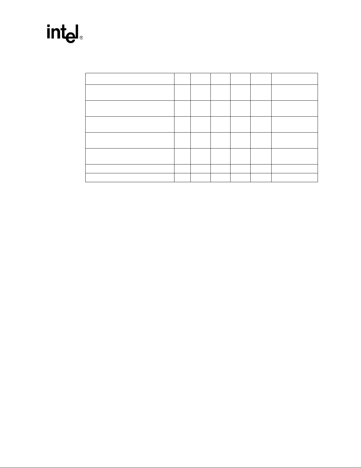
®
Intel
Celeron® Processor up to 1.10 GHz
T able 11. System Bus AC Specifications (SET Clock)
T# Parameter Min Nom Max Unit Figure Notes
System Bus Frequency
T1: BCLK Period
T2: BCLK Period Stability
T3: BCLK High Time
T4: BCLK Low Time
T5: BCLK Rise Time 0.4 1.6 ns 3 3, 8
T6: BCLK Fall Time 0. 4 1.6 ns 3 3, 8
NOTES:
1. Unless otherwise noted, all specifications in this table apply to Celeron
2. All AC timings for the AGTL+ signals are referenced to the BCLK rising edge at 1.25 V at the processor pin.
All AGTL+ signal timings (address bus, data bus, etc.) are referenced at 1.00 V at the processor pins.
3. Not 100% tested. Specified by design characterization as a clock driver requirement.
4. The internal core clock frequency is derived from the processor system bus clock. The system bus clock to
core clock ratio is determined during initialization. Individual processors will only operate at their specified
system bus frequency, either 66 MHz or 100 MHz, not both. Table 12 shows the supported ratios for each
processor.
5. The BCLK period allows a +0.5 ns tolerance for clock driver variation. See the appropriate clock synthesizer/
driver specification for details.
6. Due to the difficulty of accurately measuring clock jitter in a system, it is recommended that a clock driver be
used that is designed to meet the period stability specification into a test load of 10 to 20 pF. This should be
measured on the rising edges of adjacent BCLKs crossing 1.25 V at the processor pin. The jitter present
must be accounted for as a component of BCLK timing skew between devices.
7. The clock driver’s closed loop jitter bandwidth must be set low to allow any PLL-based device to track the
jitter created by the clock driver. The –20 dB attenuation point, as measured into a 10 to 20 pF load, should
be less than 500 kHz. This specification may be ensured by design characterization and/or measured with a
spectrum analyzer. See the appropriate clock synthesizer/driver specification for details
8. BCLK Rise time is measure between 0.5 V–2.0 V. BCLK fall time is measured between 2.0 V–0.5 V.
9. BCLK high time is measured as the period of time above 2.0 V. BCLK low time is measured as the period of
time below 0.5 V.
10.This specification applies to Pentium III
11.This specification applies to Pentium III
processors operating at a system bus frequency of 66 MHz.
processors operating at a system bus frequency of 100 MHz
66.67
100.00
10.0
10.0
2.5
2.5
2.4
2.4
1, 2
±250
±250
MHz 4
ns 3
ps
ns 3
ns 3
4, 5, 10
4, 5, 11
6, 7, 10
6, 7, 11
9, 10
9, 11
9, 10
9, 11
processors at all frequencies.
Datasheet 37
Page 38
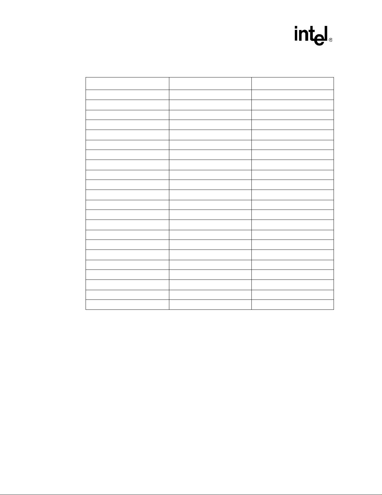
®
Intel
Celeron® Processor up to 1.10 GHz
Table 12. Valid Intel® Celeron® Processor System Bus, Core Frequency
Core Frequency (MHz) BCLK Frequency (MHz) Frequency Multiplier
266 66 4
300 66 4.5
333 66 5
366 66 5.5
400 66 6
433 66 6.5
466 66 7
500 66 7.5
533 66 8
566 66 8.5
600 66 9
633 66 9.5
667 66 10
700 66 10.5
733 66 11
766 66 11.5
800 100 8
850 100 8.5
900 100 9
950 100 9.5
1,000 100 10
1,100 100 11
NOTES:
1. C ontact your local Intel representative for the latest information on processor frequencies and/or frequency
multipliers.
2. While other bus ratios are defined, operation at frequencies other than those listed are not supported.
38 Datasheet
Page 39

®
Intel
Celeron® Processor up to 1.10 GHz
T able 13. System Bus AC Specifications (AGTL+ Signal Group) at the Processor Edge
Fingers (for S.E.P. Package)
T# Parameter Min Max Unit Figure Notes
T7’: AGTL+ Output Valid Delay 1.07 6.37 ns 4 4, 5
T8’: AGTL+ Input Setup Time 1.96 ns 5 4, 6, 7, 8
T9’: AGTL+ Input Hold Time 1.53 ns 5 4, 9
T10’: RESET# Pulse Width 1.00 ms 6 10
NOTES:
1. Unless otherwise noted, all specifications in this table apply to all Celeron processor frequencies.
2. Not 100% tested. Specified by design characterization.
3. All AC timings for the AGTL+ signals are referenced to the BCLK rising edge at 0.50 V at the processor edge
fingers. All AGTL+ signal timings (compatibility signals, etc.) are referenced at 1.00 V at the processor edge
fingers.
4. This specification applies to Intel Celeron processors operating with a 66 MHz Intel Celeron processor
system bus only.
5. Valid delay timings for these signals are specified into 50 Ω to 1.5 V and with V
6. A minimum of 3 clocks must be guaranteed between two active-to-inactive transitions of TRDY#.
7. RESET# can be asserted (active) asynchronously, but must be deasserted synchronously.
8. Specification is for a minimum 0.40 V swing.
9. Specification is for a maximum 1.0 V swing.
10.After V
CC
, and BCLK become stable.
CORE
REF at 1.0 V.
T a ble 14. System Bus AC Specifications (AGTL+ Signal Group) at the Processor Core Pins
(for S.E.P. Package)
T# Parameter Min Max Unit Figur e Notes
T7: AGTL+ Output Valid Delay 0.17 5.16 ns 4 5
T8: AGTL+ Input Setup Time 2.10 ns 5 5, 6, 7, 8
T9: AGTL+ Input Hold Time 0.77 ns 5 9
T10: RESET# Pulse Width 1.00 ms 6 7, 10
NOTES:
1. Unless otherwise noted, all specifications in this table apply to all Intel
2. These specifications are tested during manufacturing.
3. All AC timings for the AGTL+ signals are referenced to the BCLK rising edge at 1.25 V at the processor core
pin. All AGTL+ signal timings (compatibility signals, etc.) are referenced at 1.00 V at the processor core pins.
4. This specification applies to the Intel Celeron processor operating with a 66 MHz Intel Celeron processor
system bus only.
5. Valid delay timings for these signals are specified into 25 Ω to 1.5 V and with V
6. A minimum of 3 clocks must be guaranteed between two active-to-inactive transitions of TRDY#.
7. RESET# can be asserted (active) asynchronously, but must be deasserted synchronously.
8. Specification is for a minimum 0.40 V swing.
9. Specification is for a maximum 1.0 V swing.
10.After V
CC
and BCLK become stable.
CORE
®
Celeron® processor frequencies.
REF at 1.0 V.
Datasheet 39
Page 40
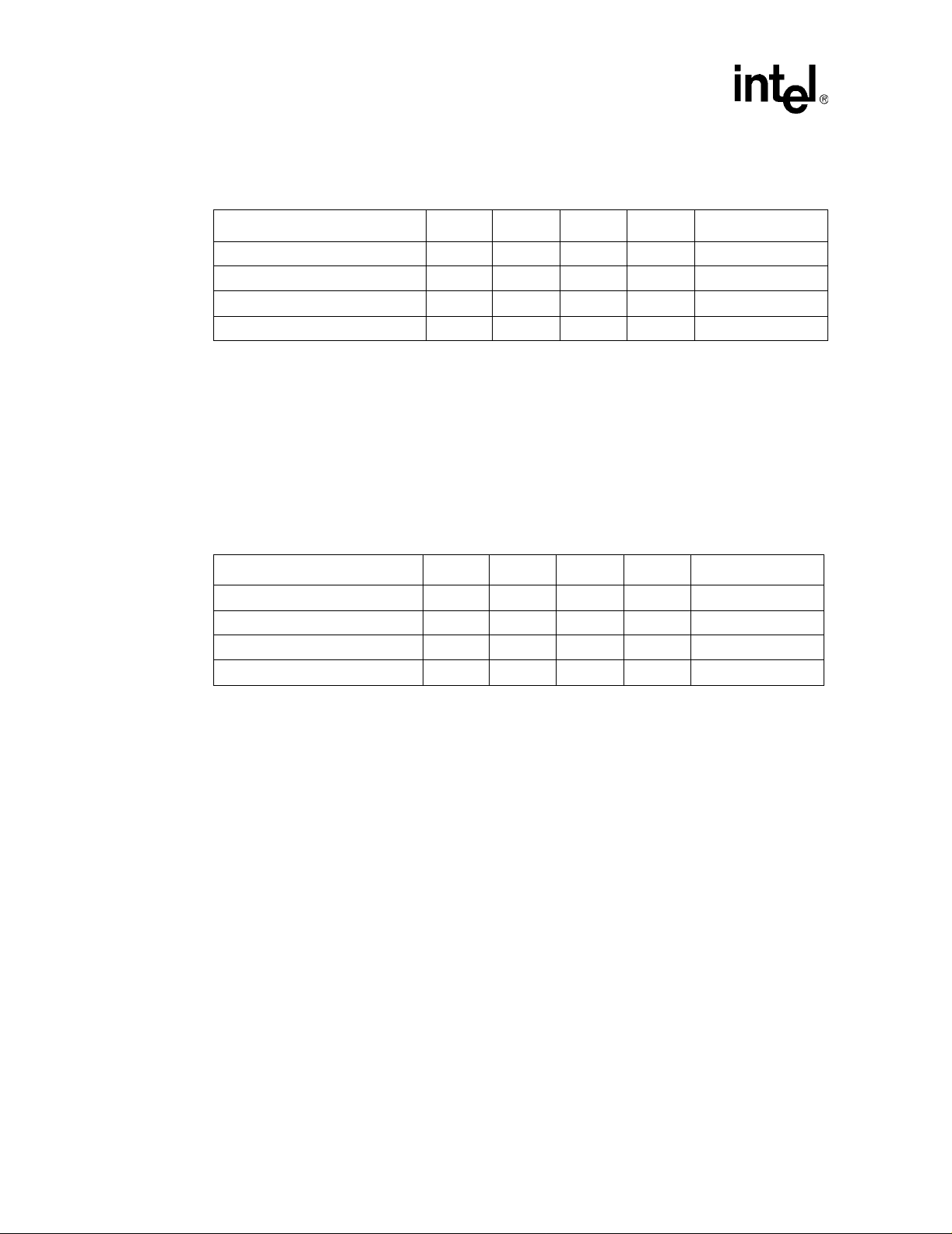
®
Intel
Celeron® Processor up to 1.10 GHz
T a ble 15. Processor System Bus AC Specifications (AGTL+ Signal Group) at the Processor
Core Pins (for PPGA Package)
T# Parameter Min Max Unit Figure Notes
T7: AGTL+ Output Valid Delay 0.30 4.43 ns 4 5
T8: AGTL+ Input Setup Time 2.10 ns 5 5, 6, 7
T9: AGTL+ Input Hold Time 0.85 ns 5
T10: RESET# Pulse Width 1.00 ms 6 7, 8
NOTES:
1. Unless otherwise noted, all specifications in this table apply to all processor frequencies.
2. These specifications are tested during manufacturing.
3. All AC timings for the AGTL+ signals are
REFerenced to the BCLK rising edge at 1.25 V at the processor pin.
All GTL+ signal timings (compatibility signals, etc.) are referenced at 1.00 V at the processor pins.
4. This spec ification applies to the processor operating with a 66 MHz system bus only.
5. Valid delay timings for these signals are specified into 25 Ω to 1.5 V and with V
REF at 1.0 V.
6. A minimum of 3 clocks must be guaranteed between two active-to-inactive transitions of TRDY#.
7. R ESE T # can be asserted (active) asynchronously, but must be deasserted synchronously.
CC
8. After V
and BCLK become stable.
CORE
Table 16. System Bus AC Specifications (AGTL+ Signal Group) at the Processor Core Pins
(for FC-PGA/FC-PGA2 Packages)
T# Parameter Min Max Unit Figur e Notes
T7: AGTL+ Output Valid Delay 0.40 3.25 ns 4 4, 10, 11
T8: AGTL+ Input Setup Time 1.20 ns 5 5, 6, 7, 10, 11
T9: AGTL+ Input Hold Time 1.00 ns 5 8, 10, 11
T10: RESET# Pulse Width 1.00 ms 7 6, 9, 10, 11
NOTES:
1. Unless otherwise noted, all specifications in this table apply to all Celeron processors at all frequencies and
cache sizes.
2. These specifications are tested during manufacturing.
3. All AC timings for the AGTL+ signals are referenced to the BCLK rising edge at 1.25 V at the processor pin.
All AGTL+ signal timings (compatibility signals, etc.) are referenced at 1.00V at the processor pins.
4. Valid delay timings for these signals are specified into 50 Ω to 1.5 V and with V
REF at 1.0 V.
5. A minimum of 3 clocks must be guaranteed between two active-to-inactive transitions of TRDY#.
6. R ESE T # can be asserted (active) asynchronously, but must be deasserted synchronously.
7. Specif ication is for a minimum 0.40 V swing from V
REF - 200 mV to VREF + 200 mV. This assumes an edge
rate of 0.3 V/ns.
8. Specification is for a maximum 1.0 V swing from V
CC
9. This should be measure d after V
10.This spec ification applies to the FC-PGA/FC-PGA2 packages runn ing at 66 MHz system bus frequency.
CORE
, VCC
TT – 1V to VTT. This assumes an edge rate of 3 V/ns.
, and BCLK become stable.
CMOS
11.This specification applies to the FC-PGA/FC-PGA2 packages running at 100 MHz system bus frequency.
40 Datasheet
Page 41

®
Intel
Celeron® Processor up to 1.10 GHz
T able 17. System Bus AC Specifications (CMOS Signal Group) at the P rocessor Edge Fingers
(for S.E.P. Package)
T# Parameter Min Max Unit Figure Note s
T14’: CMOS Input Pulse Width, except
PWRGOOD
T14B: LINT[1:0] Input Pulse Width 6 BCLKs 8 5
T15’: PWRGOOD Inactive Pulse Width 10 BCLKs 8 6, 7
NOTES:
1. Unless otherwise noted, all specifications in this table apply to all Celeron processor frequencies.
2. Not 100% tested. Specified by design characterization.
3. All AC timings for the CMOS signals are referenced to the BCLK rising edge at 0.50 V at the processor edge
fingers. All CMOS signal timings (address bus, data bus, etc.) are referenced at 1.25 V.
4. These signals may be driven asynchronously.
5. This specification only applies when the APIC is enabled and the LINT1 or LINT0 pin is configured as an
edge-triggered interrupt with fixed delivery; otherwise, specification T14 applies.
PWRGOOD must remain below V
specifications in Table 5 and BCLK has met the BCLK AC specifications in T able 10 for at least 10 clock
cycles. PWRGOOD must rise glitch-free and monotonically to 2.5 V.
6. When driven inactive or after V
7. If the BCLK signal meets its AC specification within 150 ns of turning on, then the PWRGOOD inactive pulse
width specification (T15) is waived and BCLK may start after PWRGOOD is asserted. PWRGOOD must still
remain below V
until all the voltage planes meet the voltage tolerance specifications.
IL,max
IL,max
CC
, and BCLK become stable.
CORE
2BCLKs8
(Table 6) until all the voltage planes meet the voltage tolerance
Active and
Inactive states
Table 18. System Bus AC Specifications (CMOS Signal Group) at the Processor Core Pins
(for Both S.E.P., PGA, and FC-PGA/FC-PGA2 Packages)
T# Parameter Min Max Unit Figure Notes
T14: CMOS Input Pulse Width, except
PWRGOOD
T14B: LINT[1:0] Input Pulse Width
(S.E.P.P. Only)
T15: PWRGOOD Inactive Pulse Width 10 BCLKs 8 6, 7
2BCLKs8
6BCLKs8 5
Active and
Inactive states
NOTES:
1. Unless otherwise noted, all specifications in this table apply to all Celeron processor frequencies.
2. These specifications are tested during manufacturing.
3. All AC timings for the CMOS signals are referenced to the BCLK rising edge at 1.25 V at the processor core
pins. All CMOS signal timings (address bus, data bus, etc.) are referenced at 1.25 V.
4. These signals may be driven asynchronously.
5. This specification only applies when the APIC is enabled and the LINT1 or LINT0 pin is configured as an
edge-triggered interrupt with fixed delivery; otherwise, specification T14 applies.
6. When driven inactive or after V
7. If the BCLK signal meets its AC specification within 150 ns of turning on, then the PWRGOOD inactive pulse
width specification (T15) is waived and BCLK may start after PWRGOOD is asserted. PWRGOOD must still
remain below V
PWRGOOD must remain below V
specifications in Table 5 and BCLK has met the BCLK AC specifications in T able 10 for at least 10 clock
cycles. PWRGOOD must rise glitch-free and monotonically to 2.5 V.
until all the voltage planes meet the voltage tolerance specifications.
IL,max
CC
, and BCLK become stable.
CORE
(Table 6) until all the voltage planes meet the voltage tolerance
IL,max
Datasheet 41
Page 42

®
Intel
Celeron® Processor up to 1.10 GHz
Table 19. System Bus AC Specifications (CMOS Signal Group)
T# Parameter Min Max Unit Figure Notes
T14: CMOS Input Pulse Width, except
PWRGOOD
T15: PWRGOOD Inactive Pulse Width 10 BCLKs 4, 8 5
NOTES:
1. Unless otherwise noted, all specifications in this table apply to Celeron processors at all frequencies
2. These specifications are tested during manufacturing.
3. These signals may be driven asynchronously.
4. All CMOS outputs shall be asserted for at least 2 BCLKs.
5. When driven inactive or after V
CC
CORE
2BCLKs4
, VTT, VCC
, and BCLK become stable.
CMOS
1, 2, 3, 4
Active and
Inactive states
Table 20. System Bus AC Specifications (Reset Conditions)
(for Both S.E.P. and PPGA Packages)
T# Parameter Min Max Unit Figure Notes
T16: Reset Configuration Signals (A[14:5]#,
BR0#, FLUSH#, INIT#) Setup Time
T17: Reset Configuration Signals (A[14:5]#,
BR0#, FLUSH#, INIT#) Hold Time
NOTES:
1. Unless otherwise noted, all specifications in this table apply to all Intel ®Celeron
4BCLKs6
220BCLKs6
Before deassertion
of RESET#
After clock that
deasserts RESET#
®
processor frequencies.
Table 21. System Bus AC Specifications (Reset Conditions) (for the FC-PGA/FC-PGA2
Packages)
T# Parameter Min Max Unit Figur e Notes
T16: Reset Configuration Signals
(A[14:5]#, BR0#, INIT#)
Setup Time
T17: Reset Configuration Signals
(A[14:5]#, BR0#, INIT#) Hold
Time
T18: Reset Configuration Signals
(A20M#, IGNNE#, LINT[1:0])
Setup Time
T19: Reset Configuration Signals
(A20M#, IGNNE#, LINT[1:0])
Delay Time
T20: Reset Configuration Signals
(A20M#, IGNNE#, LINT[1:0])
Hold Time
NOTES:
1. Unless otherwise noted, all specifications in this table apply to Celeron FC-PGA/FC-PGA2 processors at all
frequencies and cache sizes.
2. For a reset, the clock ratio defined by these signals must be a safe value (their final or a lower-multiplier)
within this delay unless PWRGOOD is being driven inactive.
3. These parameters apply to processor engineering samples only. For production units, the processor core
frequency will be determined through the processor internal logic.
4BCLKs7
220BCLKs7
1ms7
5BCLKs7
220BCLKs7
Before deassertion of
RESET#
After clock that
deasserts RESET#
Before deassertion of
RESET#, 3
After assertion of
RESET#, 2, 3
After clock that
deasserts RESET#, 3
42 Datasheet
Page 43

®
Intel
Celeron® Processor up to 1.10 GHz
44
T a ble 22. System Bus AC Specifications (APIC Clock and APIC I/O) at the Processor Edge
Fingers (for S.E.P. Package)
T# Parameter Min Max Unit Figure Notes
T21’: PICCLK Frequency 2.0 33.3 MHz
T22’: PICCLK Period 30.0 500.0 ns 3
T23’: PICCLK High Time 12.0 ns 3
T24’: PICCLK Low Time 12.0 ns 3
T25’: PICCLK Rise Time 0.25 3.0 ns 3
T26’: PICCLK Fall Time 0.25 3.0 ns 3
T27’: PICD[1:0] Setup Time 8.5 ns 5 5
T28’: PICD[1:0] Hold Time 3.0 ns 5 5
T29’: PICD[1:0] Valid Delay 3.0 12.0 ns 4 5, 6, 7
NOTES:
1. Unless otherwise noted, all specifications in this table apply to all Celeron processor frequencies.
2. Not 100% tested. Specified by design characterization.
3. All AC timings for the APIC I/O signals are referenced to the PICCLK rising edge at 0.7 V at the processor
edge fingers. All APIC I/O signal timings are referenced at 1.25 V at the processor edge fingers.
4. This specification applies to Intel Celeron processors operating with a 66 MHz Intel Celeron processor
system bus only.
5. Referenced to PICCLK rising edge.
6. For open drain signals, valid delay is synonymous with float delay.
7. Valid delay timings for these signals are specified to 2.5 V +5%.
Datasheet 43
Page 44

®
Intel
Celeron® Processor up to 1.10 GHz
Table 23. System Bus AC Specifications (APIC Clock and APIC I/O) at the Processor Core
Pins (For S.E.P. and PGA Packages)
T# Parameter Min Max Unit Figur e Notes
T21: PICCLK Frequency 2.0 33.3 MHz
T22: PICCLK Period 30.0 500.0 ns 3
T23: PICCLK High Time
• S.E.P.P and PPGA
•FC-PGA/FC-PGA2
T24: PICCLK Low Time
• S.E.P.P and PPGA
•FC-PGA/FC-PGA2
T25: PICCLK Rise Time 0.25 3.0 ns 3 (0.5 V–2.0 V)
T26: PICCLK Fall Time 0.25 3.0 ns 3 (2.0 V–0.5 V)
T27: PICD[1:0] Setup Time
• S.E.P.P and PPGA
•FC-PGA/FC-PGA2
T28: PICD[1:0] Hold Time 2.5 ns 5 5
T29: PICD[ 1:0] Valid Delay (S.E.P.P
and PPGA only)
T29a: PICD[1:0] Valid Delay (Rising
Edge) (FC-PGA/FC-PGA2
only)
T29b: PICD[1:0] Valid Delay (Falling
Edge) (FC-PGA/FC-PGA2
only)
11.0
10.5
11.0
10.5
8.0
5.0
1.5 10.0 ns 4 5, 6, 7
1.5 8.7 ns 4 5, 6, 8
1.5 12.0 ns 4 5, 6, 8
ns
ns
ns
ns
ns
ns
3
@>2.0 V
3
@>1.7 V
3
@<0.5 V
3
@<0.7 V
5
5
5
5
NOTES:
1. Unless otherwise noted, all specifications in this table apply to all Celeron processor frequencies.
2. These specifications are tested during manufacturing.
3. All AC timings for the APIC I/O signals are referenced to the PICCLK rising edge at 1.25 V at the processor
core pins. All APIC I/O signal timings are referenced at 1.25 V at the processor core pins.
4. This spec ification applies to Intel Celeron processors operating with a 66 MHz Intel Celeron processor
system bus only.
5. R eferenced to PICCLK rising edge.
6. For open drain signals, valid delay is synonymous with float delay.
7. Valid delay timings for these signals are specified to 2.5 V +5%.
8. Valid delay timings for these signals are specified to 1.5 V +5%.
44 Datasheet
Page 45

®
Intel
Celeron® Processor up to 1.10 GHz
Table 24. System Bus AC Specifications (APIC Clock and APIC I/O)
T# Parameter Min Max Unit Fig ur e No t e s
T21: PICCLK Frequency 2.0 33.3 MHz
T22: PICCLK Period 30.0 500.0 ns 3
T23: PICCLK High Time 10.5 ns 3 @ > 1.7 V
T24: PICCLK Low Time 10.5 ns 3 @ < 0.7 V
T25: PICCLK Rise Time 0.25 3.0 ns 3 (0.7 V–1.7 V)
T26: PICCLK Fall Time 0.25 3.0 ns 3 (1.7V–0.7 V)
T27: PICD[1:0] Setup Time 5.0 ns 5 4
T28: PICD[1:0] Hold Time 2.5 ns 5 4
T29a: PICD[1:0] Valid Delay (Rising Edge) 1.5 8.7 ns 3, 4 4, 5, 6
T29b: PICD[1:0] Valid Delay (Falling Edge) 1.5 12.0 ns 3, 4 4, 5, 6
NOTES:
1. Unless otherwise noted, all specifications in this table apply to Celeron processors at all frequencies.
2. These specifications are tested during manufacturing.
3. All AC timings for the APIC I/O signals are referenced to the PICCLK rising edge at 1.25 V at the processor
pins. All APIC I/O signal timings are referenced at 0.75 V at the processor pins.
4. Referenced to PICCLK rising edge.
5. For open drain signals, valid delay is synonymous with float delay.
6. Valid delay timings for these signals are specified into 150 Ω load pulled up to 1.5 V.
1, 2, 3
T a ble 25. System Bus AC Specifications (TAP Connection) at the Processor Edge Fingers
(For S.E.P. Package)
T# Parameter Min Max Unit Figure Notes
T30’: TCK Frequency 16.667 MHz
T31’: TCK Period 60.0 ns 3
T32’: TCK High Time 25.0 ns 3 @1.7 V
T33’: TCK Low Time 25.0 ns 3 @0.7 V
T34’: TCK Rise Time 5.0 ns 3 (0.7 V–1.7 V)
T35’: TCK Fall Time 5.0 ns 3 (1.7 V–0.7 V)
T36’: TRST# Pulse Width 40.0 ns 6 Asynchronous
T37’: TDI, TMS Setup Time 5.5 ns 9 5
T38’: TDI, TMS Hold Time 14.5 ns 9 5
T39’: TDO Valid Delay 2.0 13.5 ns 9 6, 7
T40’: TDO Float Delay 28.5 ns 9 6, 7
T41’: All Non-Tes t Outputs Valid Delay 2.0 27.5 ns 9 6, 8, 9
T42’: All Non-Te s t Inputs Setup Time 27.5 ns 9 6, 8, 9
T43’: All Non-Te s t Inputs Setup Time 5.5 ns 9 5, 8, 9
T44’: All Non-Tes t Inputs Hold Time 14.5 ns 9 5, 8, 9
NOTES:
1. Unless otherwise noted, all specifications in this table apply to all Intel ®Celeron® processor frequencies.
2. All AC timings for the TAP signals are referenced to the TCK rising edge at 0.70 V at the processor edge
fingers. All TAP signal timings (TMS, TDI, etc.) are referenced at 1.25 V at the processor edge fingers.
3. Not 100% tested. Specified by design characterization.
4. 1 ns can be added to the maximum TCK rise and fall times for every 1 MHz below 16.667 MHz.
5. Referenced to TCK rising edge.
6. Referenced to TCK falling edge.
7. Valid delay timing for this signal is specified to 2.5 V +5%.
8. Non-Test Outputs and Inputs are the normal output or input signals (besides TCK, TRST#, TDI, TDO, and
TMS). These timings correspond to the response of these signals due to TAP operations.
9. During Debug Port operation, use the normal specified timings rather than the TAP signal timings.
4
4
Datasheet 45
Page 46

®
Intel
Celeron® Processor up to 1.10 GHz
Table 26. System Bus AC Specifications (TAP Connection) at the Processor Core Pins
(for Both S.E.P. and PPGA Packages)
T# Parameter Min Max Unit Figure Notes
T30: TCK Frequency 16.667 MHz
T31: TCK Period 60.0 ns 3
T32: TCK High Time 25.0 ns 3 @1.7 V; 10
T33: TCK Low Time 25.0 ns 3 @0.7 V; 10
T34: TCK Rise Time 5.0 ns 3 (0.7 V–1.7 V);
T35: TCK Fall Time 5.0 ns 3 (1.7 V–0.7 V)
T36: TRST# Pulse Width 40.0 ns 6 Asynchronous; 10
T37: TDI, TMS Setup Time 5.0 ns 9 5
T38: TDI, TMS Hold Time 14.0 ns 9 5
T39: TDO Valid Delay 1.0 10.0 ns 9 6, 7
T40: TDO Float Delay 25.0 ns 9 6, 7, 10
T41: All Non-Test Outputs Valid Delay 2.0 25.0 ns 9 6, 8, 9
T42: All Non-Test Inputs Setup Time 25.0 ns 9 6, 8, 9, 10
T43: All Non-T est Inputs Setup Time 5.0 ns 9 5, 8, 9
T44: All Non-T est Inputs Hold Time 13.0 ns 9 5, 8, 9
4, 10
;
4, 10
NOTES:
1. Unless otherwise noted, all specifications in this table apply to all Celeron processor frequencies.
2. For the S.E.P. and PPGA packages: All AC timings for the TAP signals are referenced to the TCK rising edge
at 1.25 V at the processor core pins. All TAP signal timings (TMS, TDI, etc.) are referenced at 1.25 V at the
processor core pins.
For the FC-PGA/FC-PGA2 packages: All AC timings for the TAP signals are referenced to the TCK rising
edge at 0.75 V at the processor pins. All TAP signal timings (TMS, TDI, etc.) are referenced at 0.75 V at the
processor pins.
3. These specifications are tested during manufacturing, unless otherwise noted.
4. 1 ns can be added to the maximum TCK rise and fall times for every 1 MHz below 16.667 MHz.
5. Referenced to TCK rising edge.
6. Referenced to TCK falling edge.
7. For the S.E.P. and PPGA packages: Valid delay timing for this signal is specified to 2.5 V +5%.
For the FC-PGA/FC-PGA2 packages: Valid delay timing for this signal is specified to 1.5 V +3%.
8. Non-Test Outputs and Inputs are the normal output or input signals (besides TCK, TRST#, TDI, TDO, and
TMS). These timings correspond to the response of these signals due to TAP operations.
9. D uring Debug Port operation, use the normal specified timings rather than the TAP signal timings.
10.No t 100% tested. Specified by design characterization.
46 Datasheet
Page 47

®
Intel
Celeron® Processor up to 1.10 GHz
Table 27. System Bus AC Specifications (TAP Connection)
T# Parameter Min Max Unit Figure Notes
T30: TCK Frequency 16.667 MHz
T31: TCK Period 60.0 ns 3
T32: TCK High Time 25.0 ns 3 V
T33: TCK Low Time 25.0 ns 3 V
T34: TCK Rise Time 5.0 ns 3
T35: TCK Fall T ime 5.0 ns 3
T36: TRST# Pulse Width 40.0 ns 10 Asynchronous, 1 0
T37: TDI, TMS Setup Time 5.0 ns 9 5
T38: TDI, TMS Hold Time 14.0 ns 9 5
T39: TDO Valid Delay 1.0 10.0 ns 9 6, 7
T40: TDO Float Delay 25.0 ns 9 6, 7, 10
T41: All Non-Test Outputs Valid Delay 2.0 25.0 ns 9 6, 8, 9
T42: All Non-Test Inputs Setup Time 25.0 ns 9 6, 8, 9, 10
T43: All Non-Test Inputs Setup Time 5.0 ns 9 5, 8, 9
T44: All Non-Test Inputs Hold Time 13.0 ns 9 5, 8, 9
1, 2, 3
+ 0.200 V, 10
REF
– 0.200 V, 10
REF
– 0.200 V) –
(V
REF
+ 0.200 V),
(V
REF
4, 10
(V
+ 0.200 V) –
REF
– 0.200 V),
(V
REF
4, 10
NOTES:
1. Unless otherwise noted, all specifications in this table apply to all Celeron processors frequencies.
2. All AC timings for the TAP signals are referenced to the TCK rising edge at 0.75 V at the processor pins. All
TAP signal timings (TMS, TDI, etc.) are referenced at 0.75 V at the processor pins.
3. These specifications are tested during manufacturing, unless otherwise noted.
4. 1 ns can be added to the maximum TCK rise and fall times for every 1 MHz below 16.667 MHz.
5. Referenced to TCK rising edge.
6. Referenced to TCK falling edge.
7. Valid delay timing for this signal is specified to 1.5 V (1.25 V for AGTL platforms).
8. Non-Test Outputs and Inputs are the normal output or input signals (besides TCK, TRST#, TDI, TDO, and
TMS). These timings correspond to the response of these signals due to TAP operations.
9. During Debug Port operation, use the normal specified timings rather than the TAP signal timings.
10.Not 100% tested. Specified by design characterization.
Datasheet 47
Page 48

®
Intel
Celeron® Processor up to 1.10 GHz
Note: For Figure 3 through Figure 10, the following apply:
1. Figure 3 through Figure 10 are to be used in conjunction with Table 9 through Table 26.
2. All AC timings for the AGTL+ signals at the processor edge fingers are referenced to the
BCLK rising edge at 0.50 V. This reference is to account for trace length and capacitance on
the processor substrate, allowing the processor core to receive the signal with a reference at
1.25 V. All AGTL+ signal timings (address bus, data bus, etc.) are referenced at 1.00 V at the
processor edge fingers.
3. All AC timings for the AGTL+ signals at the processor core pins are referenced to the BCLK
rising edge at 1.25 V. All AGTL+ signal timings (address bus, data bus, etc.) are referenced at
1.00 V at the processor core pins.
4. All AC timings for the CMOS signals at the processor edge fingers are referenced to the
BCLK rising edge at 0.50 V. This reference is to account for trace length and capacitance on
the processor substrate, allowing the processor core to receive the signal with a reference at
1.25 V. All CMOS signal timings (compatibility signals, etc.) are referenced at 1.25 V at the
processor edge fingers.
5. All AC timings for the APIC I/O signals at the processor edge fingers are referenced to the
PICCLK rising edge at: 0.7 V for S.E.P. and PPGA packages and 0.75 V for the FC-PGA/
FC-PGA2 packages. All APIC I/O signal timings are referenced at 1.25 V for S.E.P. and
PPGA packages and 0.75 V for the FC-PGA/FC-PGA2 packages at the processor edge
fingers.
6. All AC timings for the TAP signals at the processor edge fingers are referenced to the TCK
rising edge at 0.70 V for S.E.P. and PPGA packages and 0.75 V for the FC-PGA/FC-PGA2
packages. All TAP signal timings (TMS, TDI, etc.) are referenced at 1.25 V for S.E.P. and
PPGA packages and 0.75 V for the FC-PGA/FC-PGA2 packages at the processor edge
fingers.
Figure 2. BCLK to Core Logic Offset
BCLK at
Edge Fingers
BCLK at
Core Logic
0.5V
T1B'
1.25V
48 Datasheet
Page 49
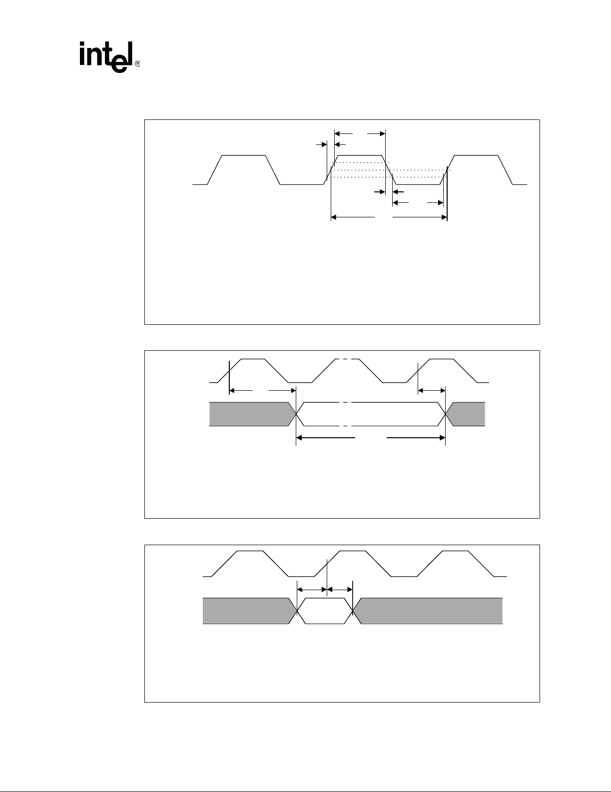
®
Intel
Celeron® Processor up to 1.10 GHz
Figure 3. BCLK*, PICCLK, and TCK Generic Clock Waveform
t
t
r
CLK
= T5, T25, T34 (Rise Time)
T
r
T
= T6, T26, T35 (Fall Time)
f
= T3, T23, T32 (High Time)
T
h
T
= T4, T24, T33 (Low Time)
l
T
= T1, T22, T31 (BLCK, TCK, PICCLK Period)
p
Note: BCLK is referenced to 0.5 V and 2.0 V. PICCLK is referenced to 0.7 V and 1.7 V.
For S.E.P. and PPGA packages, TCK is referenced to 0.7 V and 1.7 V.
For the FC-PGA package, TCK is referenced to V
0.7V (0.5V*)
h
t
f
REF
Figure 4. System Bus Valid Delay Timings
1.7V (2 .0 V *)
t
p
±200mV.
1.25V
t
l
CLK
Tx
Signal
V
Tx = T7, T11, T29a, T29b (Valid Delay)
Tpw = T14, T14B, T15 (Pulse Width)
V = 1.0V for AGTL+ signal group;
For S.E.P and PPGA packages, 1.25V for CMOS, APIC and JTAG signal groups
For FC-PGA package, 0.75V for CMOS, APIC and TAP signal groups
Figure 5. System Bus Setup and Hold Timings
CLK
Ts
Signal
Ts = T8, T12, T27 (Setup Time)
Th = T9, T13, T28 (Hold Time)
V = 1.0V for AGTL+ signal group;
For S.E.P. and PPGA packages, 1.25V for APIC and JTAG signal groups
For the FC-PGA package, 0.75V for APIC and TAP signal groups
V
Tx
Valid Valid
Tpw
Th
Valid
Datasheet 49
Page 50
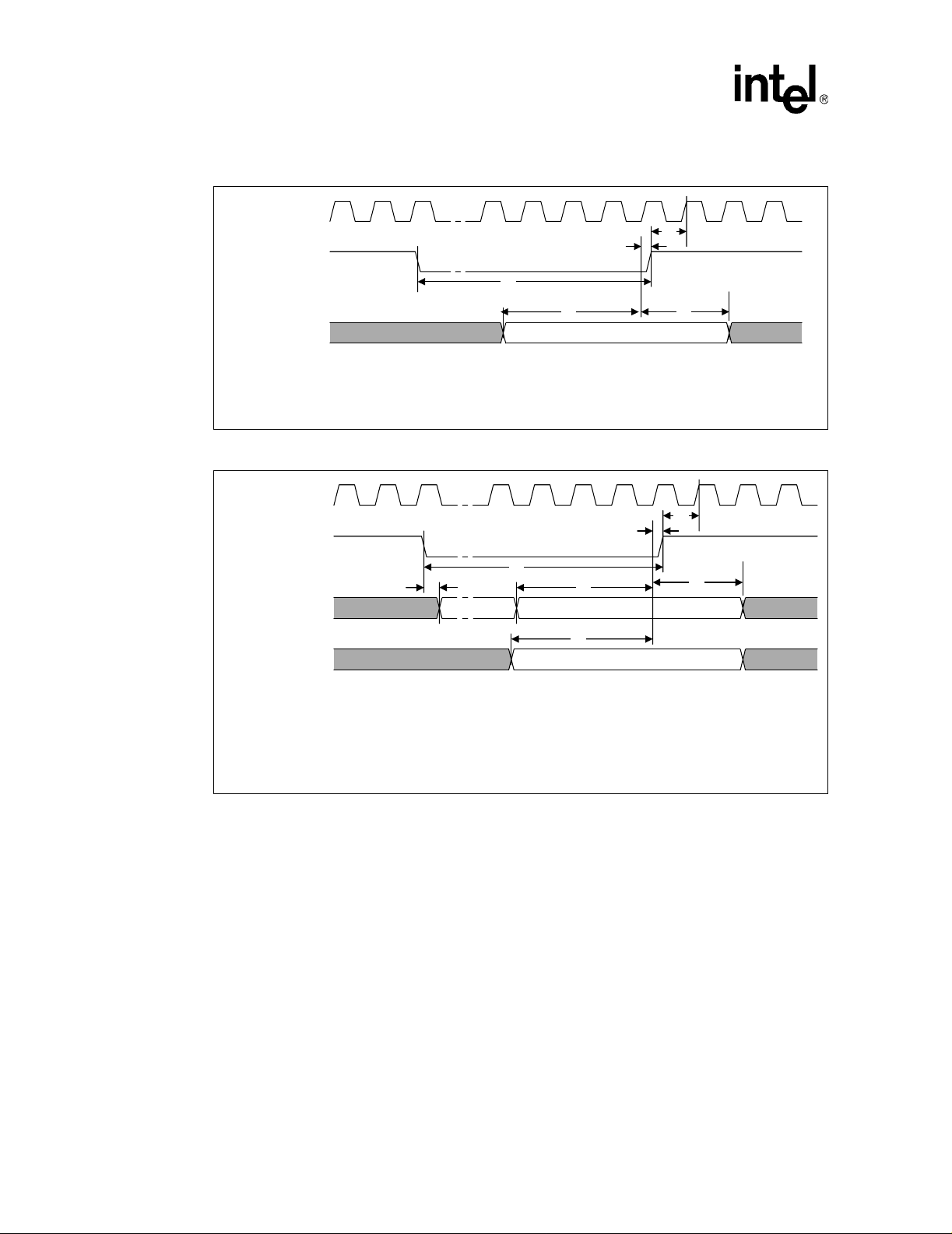
®
Intel
Celeron® Processor up to 1.10 GHz
Figure 6. System Bus Reset and Configuration Timings (For the S.E.P. and PPGA Packages)
BCLK
T
T
t
u
RESET#
T
v
Configuration
(A[14:5]#, BR0#,
FLUSH#, INT#)
T
w
Valid
= T9 (AGTL+ Input Hold Time)
T
t
= T8 (AGTL+ Input Setup Time)
T
u
= T10 (RESET# Pulse Width)
T
v
= T16 (Reset Configuration Signals (A[14:5]#, BR0#, FLUSH#, INIT#) Setup Time)
T
w
= T17 (Reset Configuration Signals (A[14:5]#, BR0#, FLUSH#, INIT#) Hold Time)
T
x
T
x
Figure 7. System Bus Reset and Configuration Timings (For the FC-PGA/FC-PGA2 Package)
BCLK
T
u
T
x
RESET#
Configuration
(A20M#, IGNNE#,
LINT[1:0])
Configuration
(A[14:5]#, BR0#,
FLUSH#, INT#)
T
t
T
T
y
v
T
z
Safe Valid
T
w
Valid
= T9 (AGTL+ Input Hold Time)
T
t
= T8 (AGTL+ Input Setup Time)
T
u
= T10 (RESET# Pulse Width)
T
v
= T16 (Reset Configuration Signals (A[14:5]#, BR0#, FLUSH#, INIT#) Setup Time)
T
w
= T17 (Reset Configuration Signals (A[14:5]#, BR0#, FLUSH#, INIT#) Hold Time)
T
x
T20 (Reset Configuration Signals (A20M#, IGNNE#, LINT[1:0]) Hold Time)
Ty = T19 (Reset Configuration Signals (A20M#, IGNNE#, LINT[1:0]) Delay Time)
Tz = T18 (Reset Configuration Signals (A20M#, IGNNE#, LINT[1:0]) Setup Time)
50 Datasheet
Page 51
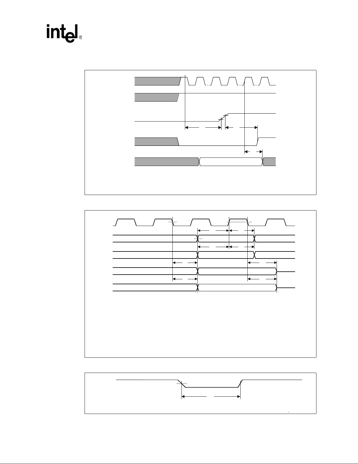
Intel
T
Figure 8. Power-On Reset and Configuration Timings
BCLK
Vcc
, VTT,
CORE
V
REF
PWRGOOD
T
RESET#
Configuration
(A20M#, IGNNE#,
INTR, NMI)
T
=T15 (PWRGOOD Inactive Pulse)
a
T
=T10 (RESET# Pulse Width)
b
T
= T20 (Reset Configuration Signals (A20M#, IGNNE#, LINT[1:0]) Hold Time) (FC-PGA)
c
®
Celeron® Processor up to 1.10 GHz
V
V
IL, max
a
IH, min
T
b
T
C
Valid Ratio
Figure 9. Test T imings (TAP Connection)
TCK
DI, TMS
Input
Signals
TDO
Output
Signals
T
T43 (All Non-Test Inputs Setup Ti me)=
r
T
T44 (All Non-Test Inputs Hold Time)=
s
T
T40 (TDO Float Delay)=
u
T
T37 (TDI, TMS Setup Time)=
v
T
T38 (TDI, TMS Hold Time)=
w
T
T39 (TDO Valid Delay )=
x
T
T41 (All Non-Test Outputs Valid Delay)=
y
T
T42 (All Non-Test Outputs Float Delay)=
z
Figure 10. Test Reset Timings
1.25V
1.25V
T
x
T
y
T
v
T
r
T
w
T
s
T
u
T
z
TRST#
T
T37 (TRST# Pulse Width)=
q
1.25V
T
q
Datasheet 51
Page 52
®
Intel
Celeron® Processor up to 1.10 GHz
3.0 System Bus Signal Simulations
Signals driven on the Celeron processor system bus should meet signal quality specifications to
ensure that the components read data proper ly and to ensur e that incomi ng signal s do not af fect the
long term reliability of the component. Specifications are provided for simulation at the processor
core; guidelines are provided for correlation to the processor edge fingers. These edge finger
guidelines are intended for use during testing and measurement of system signal integrity.
Violations of these guidelines are permitted, but if they occur, simulation of signal quality at the
processor core should be performed to ensure that no violations of signal quality specifications
occur. Meeting the specifications at the processor core in Table 28, Table 31, and Table 34 ensures
that signal quality effects will not adversely affect processor operation, but does not necessarily
guarantee that the guidelines in Table 30, Table 33, and Table 35 will be met.
3.1 System Bus Clock (BCLK) Signal Quality Specifications and Measurement Guidelines
Table 28 describes the BCLK signal quality specifications at the processor core for both S.E.P. and
PPGA Packages. Table 29 shows the BCLK and PICCLK signal quality specifications at the
processor core for the FC-PGA/FC-PGA2 packages. Table 30 describes guidelines for signal
quality measurement at the processor edge fingers. Figure 11 describes the signal quality waveform
for the system bus clock at the processor core pins; Figure 12 describes the signal quality
waveform for the system bus clock at the processor edge fingers.
T able 28. BCLK Signal Quality Specifications for Simulation at the Processor Core
(for Both S.E.P. and PPGA Packages)
T# Parameter Min Nom Max U nit Figure Notes
V1: BCLK VIL 0.5 V 11
V2: BCLK V
V3: V
V4: Rising Edge Ringback 1.7 V 11 3
V5: Falling Edge Ringback 0.7 V 11 3
NOTES:
1. Unless otherwise noted, all specifications in this table apply to all Celeron processor frequencies.
2. This is the Intel Celeron processor system bus clock overs hoot and undershoot specification for 66 MHz
system bus operation.
3. The rising and falling edge ringback voltage specified is the minimum (rising) or maximum (falling) absolute
voltage the BCLK signal can dip back to after passing the V
specification is an absolute value.
IH 2.0 V 11 2
IN Absolute Voltage Range –0.7 3.5 V 11 2
IH (rising) or VIL (falling) voltage limits. This
52 Datasheet
Page 53
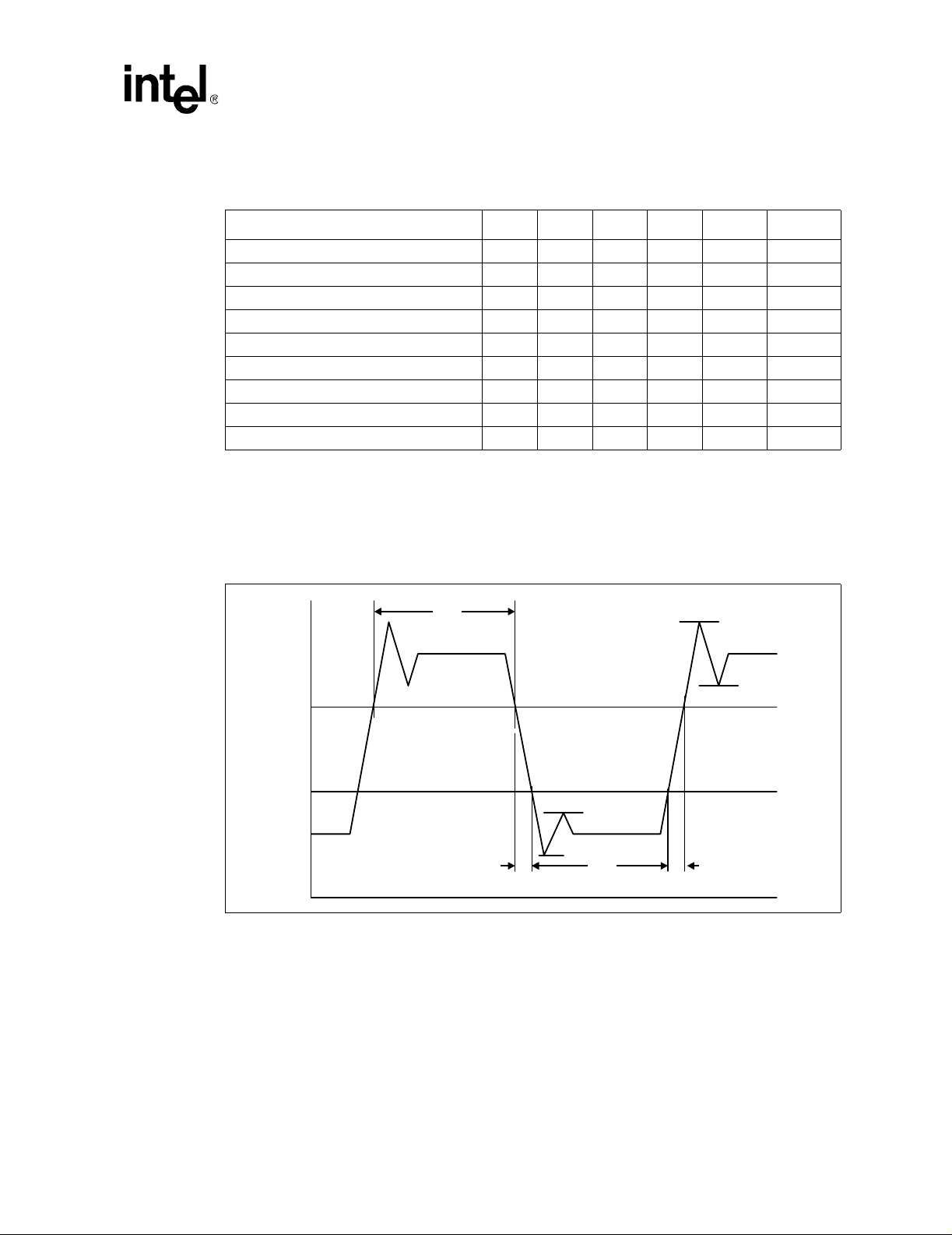
®
Intel
Celeron® Processor up to 1.10 GHz
T a ble 29. BCLK/PICCLK Signal Quality Specifications for Simulation at the Processor Pins
(for the FC-PGA/FC-PGA2 Packages)
T# Parameter Min Nom Max Unit Figure Notes
V1: BCLK VIL 0.50 V 11
V1: PICCLK V
V2: BCLK V
V2: PICCLK V
V3: V
IN Absolute Voltage Range –0.58 3.18 V 11
V4: BCLK Rising Edge Ringback 2.00 V 11 2
V4: PICCLK Rising Edge Ringback 2.00 V 11 2
V5: BCLK Falling Edge Ringback 0.50 V 11 2
V5: PICCLK Falling Edge Ringback 0.70 V 11 2
NOTES:
1. Unless otherwise noted, all specifications in this table apply to FC-PGA/FC-PGA2 processors frequencies
and cache sizes.
2. The rising and falling edge ringback voltage specified is the minimum (rising) or maximum (falling) absolute
voltage the BCLK/PICCLK signal can dip back to after passing the V
This specification is an absolute value.
IL 0.70 V 11
IH 2.00 V 11
IH 2.00 V 11
IH (rising) or VIL (falling) voltage limits.
Figure 11. BCLK, TCK, PICCLK Generic Clock Waveform at the Processor Core Pins
V2
V1
T3
V5
T6 T4 T5
V3
V3
V4
Datasheet 53
Page 54
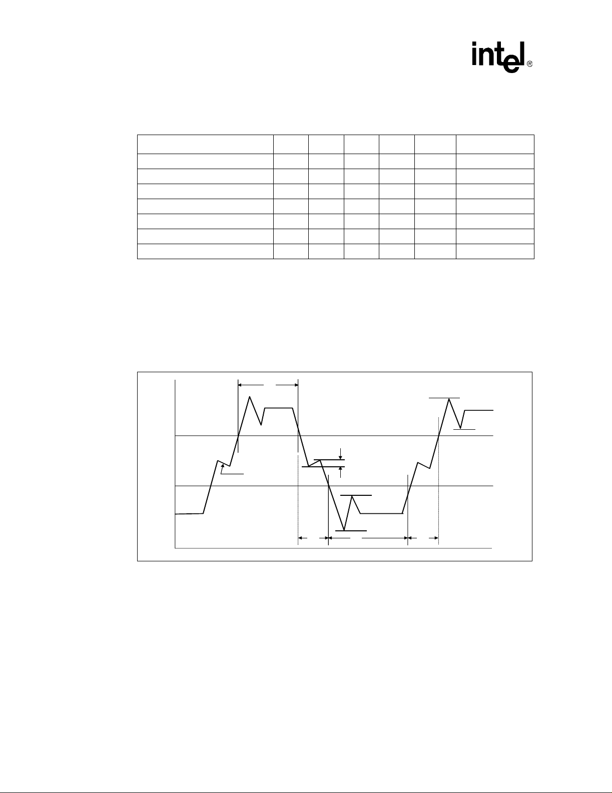
®
V
V
Intel
Celeron® Processor up to 1.10 GHz
Table 30. BCLK Signal Quality Guidelines for Edge Finger Measurement
(for the S.E.P. Package)
T# Parameter Min Nom Max Unit Figure Notes
V1’: BCLK V
V2’: BCLK V
V3’: V
IL
IH
IN Absolute Voltage Range –0.5 3.3 V 12 2
2.0 V 12
0.5 V 12
V4’: Rising Edge Ringback 2.0 V 12 3
V5’: Falling Edge Ringback 0.5 V 12 3
V6’: T
line Ledge Voltage 1.0 1.7 V 12 At Ledge Midpoint
V7’: Tline Ledge Oscillation 0.2 V 12 Peak-to-Peak
NOTES:
1. Unless otherwise noted, all specifications in this table apply to all Celeron processor frequencies.
2. This is the Intel Celeron processor system bus clock overs hoot and undershoot measur ement guideline.
3. The rising and falling edge ringback voltage guideline is the minimum (rising) or maximum (falling) absolute
voltage the BCLK signal may dip back to after passing the V
guideline is an absolute value.
(rising) or VIL (falling) voltage limits. This
IH
4. The BCLK at the processor edge fingers may have a dip or ledge midway on the rising or falling edge. The
midpoint voltage level of this ledge should be within the range of the guideline.
5. The ledge (V7) is allowed to have peak-to-peak oscillation as given in the guideline.
Figure 12. BCLK, TCK, PICCLK Generic Clock Waveform at the Processor Edge Fingers
T3
V3
2
V4
4
5
V7
V6
1
T6 T4 T5
V5
V3
54 Datasheet
Page 55

®
Intel
Celeron® Processor up to 1.10 GHz
3.2 AGTL+ Signal Quality Specifications and Measurement Guidelines
Many scenarios have been simulated to generate a set of AGTL+ lay out g ui delines which are
available in AP-585, Pentium
the Pentium
®
II Processor Developer's Manual (Order Number 243502) for the AGTL+ buffer
®
II Processor AGTL+ Guidelines (Order Number 243330). Refer to
specification.
Table 31 provides the AGTL+ signal quality specifications (for both the S.E.P. and PPGA
Packages) for use in simulating signal quality at the processor core. Table 32 provides the AGTL+
signal quality specifications (for the FC-PGA/FC-PGA2 packages) for use in simulating signal
quality at the processor core. Table 33 provides AG TL+ signal qu ality guidelines for measuri ng and
testing signal quality at the processor edge fingers. Figure 13 describes the si gnal qualit y wa veform
for AGTL+ signals at the processor core and edge fingers. For more information on the AGTL+
interface, see the Pentium
®
II Processor Developer's Manual (Order Number 243502).
T able 31. AGTL+ Signal Groups Ringback Tolerance Specifications at the Processor Core
(For Both the S.E.P. and PPGA Packages)
T# Parameter Min Unit Figure Notes
: Overshoot 100 mV 13 4
α
τ: Minimum Time at High 1.00 ns 13 4
ρ: Amplitude of Ringback –100 mV 13 4, 5
φ: Final Settling Voltage 100 mV 13 4
δ: Duration of Squarewave Ringback N/A ns 13
NOTES:
1. Unless otherwise noted, all specifications in this table apply to all Celeron processor frequencies.
2. Specifications are for the edge rate of 0.3 – 0.8 V/ns. See Figure 13 for the generic waveform.
3. All values specified by design characterization.
4. This specification applies to Inte l Celeron processors operating with a 66 MHz Intel Celeron processor
system bus only.
5. Ringback below V
REF + 20 mV is not supported.
Ta ble 32. AGTL+ Signal Groups Ringback Tolerance Specifications at the Processor Pins
(For FC-PGA/FC-PGA2 Packages)
T# Parameter Min Unit Figure Notes
: Overshoot 100 mV 13 4, 8, 9, 10
α
τ: Minimum Time at High 0.50 ns 13 9
ρ: Amplitude of Ringback –200 mV 13 5, 6, 7, 8
φ: Final Settling Voltage 200 mV 13 8
δ: Duration of Squarewave Ringback N/A ns 13
NOTES:
1. Unless otherwise noted, all specifications in this table apply to all Celeron processor frequencies.
2. Specifications are for the edge rate of 0.3 – 0.8V/ns. See Figure 13 for the generic waveform.
3. All values specified by design characterization.
4. See Table 36 for maximum allowable overshoot.
5. Ringback between V
flight time measurements to be adjusted as described in the Intel AGTL+ Specifications (
Developers Manual
6. Intel recommends simulations not exceed a ringback value of V
sources of system noise.
7. A negative value for
signal cannot ringback below V
φ and ρ: are measured relative to VREF. α: is measured relative to VREF + 200 mV.
8.
9. All Ringback entering the Overdrive Region must have flight time correction.
10.Overshoot specifications for Ringback do not correspond to Overshoot specifications in Section 3.4.
REF + 100 mV and VREF + 200 mV or VREF – 200 mV and VREF – 100 mVs requires the
Intel®Pentium®II
). Ringback below VREF + 100 mV or above VREF – 100 mV is not supported.
REF ±200 mV to allow margin for other
ρ indicates that the amplitude of ringback is above VREF. (i.e., φ = –100 mV specifies the
REF + 100 mV).
Datasheet 55
Page 56
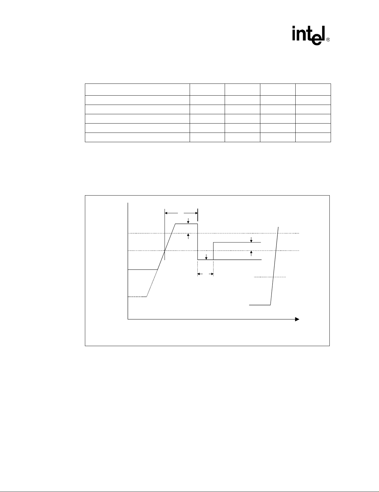
®
Intel
Celeron® Processor up to 1.10 GHz
Table 33. AGTL+ Signal Groups Ringback Tolerance Guidelines for Edge Finger
Measurement on the S.E.P. Package
T# Parameter Min Unit Figure Notes
α
’: Overshoot 100 mV 13
τ’: Minimum Time at High 1.5 ns 13 4
ρ’: Amplitude of Ringback –250 mV 13 4, 5
φ’: Final Settling Voltage 250 mV 13 4
δ’: Duration of Squarewave Ringback N/A ns 13
NOTES:
1. Unless otherwise noted, all guidelines in this table apply to all Celeron processor frequencies.
2. Guidelines are for the edge rate of 0.3 – 0.8 V/ns. See Figure 13 for the generic waveform.
3. All values specified by design characterizat ion.
4. This guideline applies to Intel Celeron processors operating with a 66 MHz system bus only.
5. R ingback below V
REF + 250 mV is not supported.
Figure 13. Low to High AGTL+ Receiver Ringback Toler ance
V +0.2
REF
V
REF
V –0.2
REF
V
start
Note: High to Low case is anal ogous.
τ
α
φ
ρ
δ
Time
0.7V Clk Ref
Clock
56 Datasheet
Page 57
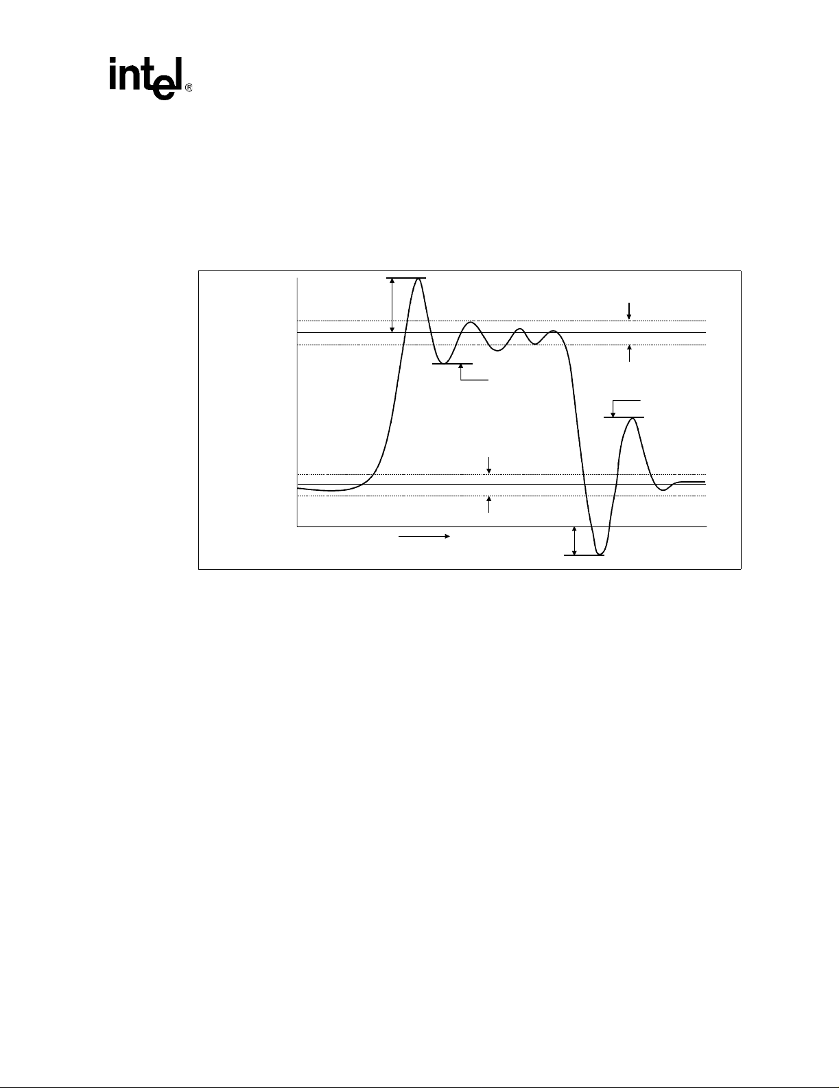
®
Intel
Celeron® Processor up to 1.10 GHz
3.3 Non-AG TL+ Signal Qualit y Specifications and Measurement Guidelines
There are three signal quality parameters defined for non-AGTL+ signals: overshoot/undershoot,
ringback, and settling limit. All three signal quality parameters are shown in Figure 14 for the nonAGTL+ signal group.
Figure 14. Non-AGTL+ Overshoot/Undershoot, Settling Limit, and Ringback
Overshoot
V
HI
Settling Limit
V
LO
V
SS
NOTES:
1. For the FC-PGA/FC-PGA2 packages, V
PWRGOOD. V
Section 3.1.
= 2.5 V for BCLK, PICCLK, and PWRGOOD. BCLK and PICCLK signal quality is detailed in
HI
Time
= 1.5 V for all non-AGTL+ signals except for BCLK, PICCLK, and
HI
3.3.1 Overshoot/Undershoot Guidelines
Rising-Edge
Ringback
Undershoot
Settling Limit
Falling-Edge
Ringback
Overshoot (or undershoot) is the absolute value of the maximum voltage above the nominal high
voltage or below V
SS. The overshoot/undershoot guideline limits transitions beyond VCC or VSS
due to the fast signal edge rates. (See Figure 14 for non-AGTL+ signals.) The processor can be
damaged by repeated overshoot events on the volt age t oleran t buffers if the charge is lar ge enou gh
(i.e., if the overshoot is great enough). The PPGA and S.E.P. packages have 2.5 V tolerant buffers
and the FC-PGA/FC-PGA2 packages has 1.5 V or 2.5 V tolerant buffers.
However, excessive ringback is the dominant detrimental system timing effect resulting from
overshoot/undershoot (i.e., violating the overshoot/undershoot guideline will make satisfying the
ringback specification difficult). The overshoot/undershoot guideline is 0.7 V for the PPGA
and S.E.P. packages and 0.3 V for the FC-PGA/FC-PGA2 packages and assumes the absence
of diodes on the input. These guidelines should be verified in simulations without the on-chip
ESD prote cti on d i od es p resent because the diodes will begin clamping the signals (2.5 V tolerant
signals for the S.E.P. and PPGA packages, and 2.5 V or 1.5 V tolerant signals for the FC-PGA/
FC-PGA2 packages) beginning at approximately 0.7 V above the appropriate supply and 0.7 V
below V
SS. If signals are not reaching the clamping voltage, this will not be an issue. A system
should not rely on the diodes for overshoot/undershoot protection as this will negatively affect the
life of the components and make meeting the ringback specification very difficult.
Datasheet 57
Page 58

®
Intel
Celeron® Processor up to 1.10 GHz
3.3.2 Ringback Specification
Ringback refers to the amount of reflection seen after a signal has switched. The ringback
specification is the voltage that the signal rings back to after achieving its maximum absolute
value. (See Figure 14 for an illustration of ringback.) Excessive ringback can cause false signal
detection or extend the propagation delay. The ringback specification applies to the input pin of
each receiving agent. Violations of the signal ringback specification are not allowed under any
circumstances for non-AGTL+ signals.
Ringback can be simulated with or without the input protection diodes that can be added to the
input buffer model. However, signals that reach the clamping voltage should be evaluated further.
See Ta ble 34 for the signal ringback specifications for non-AGTL+ signals for simulations at the
processor core, and Table 35 for guidelines on measuring ringback at the edge fingers. Table 36
lists the ringback specifications for the FC-PGA/FC-PGA2 packages.
T able 34. Signal Ringback Specifications for Non-AGTL+ Signal Simulation at the Processor
Core (S.E.P. and PPGA Packages)
Input Signal Group Transition
Non-AGTL+ Signals 0 → 11.7V14
Non-AGTL+ Signals 1 → 00.7V14
NOTE:
1. Unless otherwise noted, all specifications in this table apply to all Celeron processor frequencies.
Maximum Ringback
(with Input Diodes Pr esent) Unit Figure Notes
Ta ble 35. Signal Ringback Guidelines for Non-AGTL+ Signal Edge Finger Measurement
(S.E.P. Package)
Input Signal Group Transition
Non-AGTL+ Signals 0 → 12.0V14
Non-AGTL+ Signals 1 → 00.7V14
NOTE:
1. Unless otherwise noted, all specifications in this table apply to all Celeron processor frequencies.
Maximum Ringback
(with Input Diodes Pr esent) Unit Figure Notes
T able 36. Signal Ringback Specifications for Non-AGTL+ Signal Simulation at the Processor
Pins (FC-PGA/FC-PGA2 Packages)
Input Signal Group Transition
Non-AGTL+ Signals 0 → 1VREF + 0.200 V 16
PWRGOOD 0 → 12.0V16
Non-AGTL+ Signals 1 → 0V
Maximum Ringback
(with Input Diodes Present) Unit Figure
REF – 0.200 V 16
NOTES:
1. Unless otherwise noted, all specifications in this table apply to all FC-PGA/FC-PGA2 processor frequencies
and cache sizes.
58 Datasheet
Page 59

®
Intel
Celeron® Processor up to 1.10 GHz
3.3.3 Settling Limit Guideline
Settling limit defines the maximum amount of ringing at the receiving pin that a signal must reach
before its next transition. The amount allowed is 10 percent of the total signal swing (V
HI
above and below its final value. A signal should be within the settling limits of its final value, when
either in its high state or low state, before it transitions again.
Signals that are not within their settling limit before transitioning are at risk of unwanted
oscillations which could jeopardize signal integrity. Simulations to verify settling limit may be
done either with or without the input protection diodes present. Violation of the settling limit
guideline is acceptable if simulations of 5 to 10 successive transitions do not show the amplitude of
the ringing increasing in the subsequent transitions.
3.4 AGTL+ Signal Quality Specifications and Measurement Guidelines (FC-PGA/FC-PGA2 Packages)
3.4.1 Overshoot/Undershoot Guidelines (FC-PGA/FC-PGA2 Packages)
Overshoot (or undershoot) is the absolute value of the maximum voltage above the nominal high
voltage or below V
signal edge rates. The processor can be damaged by repeated overshoot events on 1.5 V or 2.5 V
tolerant buffers if the charge is large enough (i.e., if the overshoot is great enough). Determining
the impact of an overshoot/undershoot condition requires knowledge of the magnitude, the pulse
direction and the activity factor (AF). Permanent damage to the processor is the likely result of
excessive overshoot/undershoot. Violating the overshoot/undershoot guideline will also make
satisfying the ringback specification difficult.
SS. The overshoot guideline limits transitions beyond VCC or VSS due to the fast
– V
LO
)
When performing simulations to determine impact of overshoot and overshoot, ESD diodes must
be properly characterized. ESD protection diodes do not act as voltage clamps an d will not provide
overshoot or undershoot protection. ESD diodes modeled within Intel I/O Buffer models do not
clamp undershoot or overshoot and will yield correct simulation results. If other I/O buffer models
are being used to characterize the FC-PGA/FC-PGA2 processor performance, care must be taken
to ensure that ESD models do not clamp extreme voltage levels. Intel I/O Buffer models also
contain I/O capacitance characterization. Therefore, removing the ESD diodes from an I/O Buffer
model will impact results and may yield excessive overshoot/undershoot.
3.4.2 Overshoot/Undershoot Magnitude (FC-PGA/FC-PGA2 Packages)
Magnitude describes the maximum potential difference between a signal and its voltage reference
level, V
using one probe (probe to signal and GND lead to V
V
signal undershoot. Today’s oscillosco pes can easily calcula te the true un dershoot wa veform using a
Math function where the Signal waveform is subtracted from the V
undershoot waveform can also be obtained with the following oscilloscope data file analysis:
Note: The converted undershoot waveform appears as a positive (overshoot) signal.
Note: Overshoot (rising edge) and undershoot (falling edge) conditions are separate and their impact
must be determined independently.
SS (overshoot) and VTT (undershoot). While overshoot can be measured relative to VSS
SS), undershoot must be measured relative to
TT. This can be accomplished by simultaneously measuring the VTT plane while measuring the
TT waveform. The true
Converted Undershoot Waveform = VTT– Signal_measured
Datasheet 59
Page 60

®
Intel
Celeron® Processor up to 1.10 GHz
After the true waveform conversion, the undershoot/overshoot specifications shown in Table 38
and Table 39 can be applied to the converted undershoot waveform using the same magnitude and
pulse duration specifications used with an overshoot waveform.
Overshoot/undershoot magni tude levels mus t observe the Absolut e Maximum Speci fications lis ted
in Table 38 and Table 39. These specifications must not be violated at any time regardless of bus
activity or system state. Within these specifications are threshold levels that define different
allowed pulse durations. Provided that the magnitude of the overshoot/undershoot is within the
Absolute Maximum Specifications (2.18V), the puls e magnitude, duration and activity factor must
all be used to determine if the overshoot/undershoot pulse is within specifications.
3.4.3 Overshoot/Undershoot Pulse Duration (FC-PGA/FC-PGA2 Packages)
Pulse duration describes the total time an overshoot/undershoot event exceeds the overshoot/
undershoot reference voltage (Vos_ref = 1.635 V). The total time could encompass several
oscillations above the reference voltage. Multiple overshoot/undershoot pulses within a single
overshoot/undershoot event may need to be measured to determine the total pulse duration.
Note: Oscillations below the reference voltage can not be subtracted from the total overshoot/undershoot
pulse duration.
Note: Multiple Overshoot/Undershoot events occurring within the same clock cycle must be considered
together as one event. Using the worst case Overshoot/Undershoot Magnitude, sum together the
individual Pulse Durations to determine the total Overshoot/Undershoot Pulse Duration for that
total even t .
3.4.4 Acti vity Factor (FC-PGA/FC-PGA2 Packages)
Activity Factor (AF) describes the frequency of overshoot (or undershoot) occurrence relative to a
clock. Since the highest frequency of assertion of an AGTL+ or a CMOS signal is every other
clock, an AF = 1 indicates that the specific overshoot (or undershoot) waveform occurs EVERY
OTHER clock cycle. Thus, an AF = 0.01 indicates that the specific overshoot (or undershoot)
waveform occurs one time in every 200 clock cycles.
The specifications provided in Table 38 and Table 39 show the Maximum Pulse Duration allowed
for a given Overshoot/Undershoot Magnitude at a specific Activity Factor. Each table entry is
independent of all others, meaning that the Pulse Duration reflects the existence of overshoot/
undershoot events of that magnitude ONLY. A platform with an overshoot/undershoot that just
meets the pulse duration for a specific magnitude where the AF < 1, means that there can be NO
other overshoot/undershoot events, even of lesser magnitude (note that if AF = 1, then the event
occurs at all times and no other events can occur).
Note: Activity factor for AGTL+ signals is referenced to BCLK frequency.
Note: Activity factor for CMOS signals is referenced to PICCLK frequency.
60 Datasheet
Page 61

®
Intel
Celeron® Processor up to 1.10 GHz
3.4.5 Reading Overshoot/Undershoot Specification Tables (FC-PGA/ FC-PGA2 Packages)
The overshoot/undershoot specification for the FC-PGA/FC-PGA2 packages processor is not a
simple single value. Instead, many factors are needed to determine the over/undershoot
specification. In additi on to t he mag nit ude o f the overshoot, the following parameters must also be
known: the junction temperature the processor will be operating, the width of the overshoot (as
measured above 1.635 V) and the Activity Factor (AF). To determine the allowed overshoot for a
particular overshoot event, the following must be done:
1. Determine the signal group that particular signal falls into. If the signal is an AGTL+ signal
operating with a 66 MHz system bus, use Table 38 (66 MHz AGTL+ signal group). If the
signal is a CMOS signal, use Table 39 (33 MHz CMOS signal group).
2. Determine the maximum junction temperature (Tj) for the range of pro cessor s that the system
will support (80
o
C or 90oC).
3. Determine the Magnitude of the overshoot (relative to V
4. Determine the Activity Factor (how often does this overshoot occur?)
5. From the appropriate Specification table, read off the Maximum Pulse Duration (in ns)
allowed.
6. Compare the specified Maximum Pulse Duration to the signal being measured. If the Pulse
Duration measured is less than the Pulse Duration shown in the table, then the signal meets the
specifications.
The above procedure is similar for undershoots after the undershoot waveform has been converted
to look like an overshoot. Undershoot events must be analyzed separately from Overshoot events
as they are mutually exclusive.
Table 37 shows an example of how the maximum pulse duration is determined for a given
waveform.
T a ble 37. Example Platform Information
Required Information Maximum Platform Support Notes
FSB Signal Group 66 MHz AGTL+
Max Tj 90 °C
Overshoot Magnitude 2.13V Measured Value
Activity Factor (AF) 0.1
SS)
Measured overshoot occurs on
average every 20 clocks
NOTES:
1. Corresponding Maximum Pulse Duration Specification – 3.2 ns
2. Pulse Duration (measured) – 2.0 ns
Given the above parameters, and using Table 38 (90oC/AF=0.1 column) the maximum allowed
pulse duration is 3.2 ns. Since the measured pulse duration is 2.0ns, this parti cul ar ov ers hoo t event
passes the overshoot specifications, although this doesn't guarantee that the combined overshoot/
undershoot events meet the specifications.
Datasheet 61
Page 62

®
Intel
Celeron® Processor up to 1.10 GHz
3.4.6 Determining if a System meets the Overshoot/Undershoot
Specifications (FC-PGA/FC-PGA2 Pack ages)
The overshoot/undershoot specifications listed in the following tables specify the allowable
overshoot/undershoot for a single overshoot/undershoot event. However most systems will have
multiple overshoot and/or undershoot events that each have their own set of parameters (duration,
AF and magnitude). While each overshoot on its own may meet the overshoot specification, when
the total impact of all overshoot events is accounted for, the system may fail. A guideline to ensure
a system passes the oversh oot and undershoot specifications is shown below. It is important to meet
these guidelines; otherwise, contact your Intel field representative.
1. Insure no signal (CMOS or AGTL+) ever exceed the 1.635 V; OR
2. If only one oversho ot/un dershoot event magn itude o ccurs, ensure it meets the ove r/unders hoot
specifications in the following tables; OR
3. If multiple overshoots and/or multiple undershoots occur, measure the worst case pulse
duration for each magnitude and compare the r esults against th e AF = 1 specification s. If all of
these worst case overshoot or undershoot events meet the specifications
(measured time < specifications) in the table (where AF=1), then the system passes.
The following notes apply to Table 38 and Table 39.
NOTES:
1. Overshoot/Undershoot Magnitude = 2.18 V is an Absolute value and should never be exceeded
2. Overshoot is measured relative to V
3. Undershoot is measured relative to VTT
4. Overshoot/Undershoot Pulse Duration is measured relative to 1.635 V.
5. Ringbacks below V
TT can not be subtracted from Overshoots/Undershoots.
6. Lesser Undershoot does not allocate longer or larger Overshoot.
7. Consult the appropriate layout guidelines provided in the specific platform design guide.
8. All values specified by design characterization.
SS
Table 38. 66 MHz AGTL+ Signal Group Overshoot/Undershoot Tolerance at Processor Pins
(FC-PGA/FC-PGA2 Packages)
Overshoot/
Undershoot
Magnitude
2.18 V 30 3.8 0.38 18 1.8 0.18
2.13 V 30 7.4 0.74 30 3.2 0.32
2.08 V 30 13.6 1.36 30 6.4 0.64
2.03 V 30 25 2.5 30 12 1.1
1.98 V 30 30 4.56 30 22 2
1.93 V 30 30 8.2 30 30 3.8
1.88 V 30301530306.8
NOTES:
1. BCLK period is 30.0 ns.
2. Measurements taken at the processor socket pins on the solder-side of the motherboard.
Maximum Pulse Duration at Tj = 80 °C
(ns)
AF = 0.01 AF = 0.1 AF = 1 AF = 0.01 AF = 0.1 AF = 1
Maximum Pulse Duration at Tj = 90 °C
(ns)
62 Datasheet
Page 63

®
Intel
Celeron® Processor up to 1.10 GHz
Table 39. 33 MHz CMOS Signal Group Overshoot/Undershoot Tolerance at Processor Pins
(FC-PGA/FC-PGA2 Packages)
Overshoot/
Undershoot
Magnitude
2.18 V 60 7.6 0.76 36 3.6 0.36
2.13 V 60 14.8 1.48 60 6.4 0.64
2.08 V 60 27.2 2.7 60 12.8 1.2
2.03 V 60 50 5 60 24 2.2
1.98 V 60 60 9.1 60 44 4
1.93 V 60 60 16.4 60 60 7.6
1.88 V 60 60 30 60 60 13.6
NOTES:
1. PICCLK period is 30 ns.
2. Measurements taken at the processor socket pins on the solder-side of the motherboard.
Maximum Pulse Duration at Tj = 80 °C
(ns)
AF = 0.01 AF = 0.1 AF = 1 AF = 0.01 AF = 0.1 AF = 1
Maximum Pulse Duration at Tj = 90 °C
Figure 15. Maximum Acceptable AGTL+ Overshoot/Undershoot Waveform
(FC-PGA/FC-PGA2 Packages)
Time Dependent
Overshoot
2.18V
2.08V
1.98V
1.88V
1.635V
Max
V
TT
(ns)
Converted Undershoot
Waveform
Vss
Overshoot
Magnitude
Undershoot
Magnitude
Overshoot
Magnitude
= Signal - Vss
= V
- Signal
TT
Undershoot
Magnitude
Time Dependent
Undershoot
Datasheet 63
Page 64
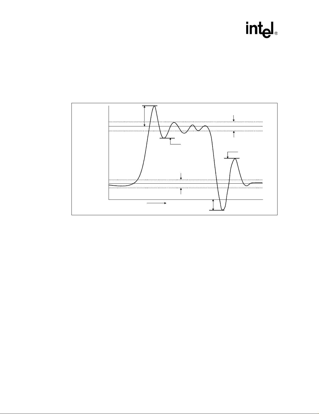
®
Intel
Celeron® Processor up to 1.10 GHz
3.5 Non-AG TL+ Signal Quality Specifications and Meas urement Guidelines
There are three signal quality parameters defined for non-AGTL+ signals: overshoot/undershoot,
ringback, and settling limit. All three signal quality parameters are shown in Figure 16 for the nonAGTL+ signal group.
Figure 16. Non-AG TL+ Overshoot/Undershoot, Settling Limit, and Ringback
1
Overshoot
V
HI
Rising-Edge
Ringback
Settling Limit
V
LO
V
SS
NOTES:
1. V
= 1.5 V for all non-AGTL+ signals except for BCLK, PICCLK, and PWRGOOD. V
HI
PICCLK, and PWRGOOD. BCLK and PICCLK signal quality is detailed in Section 3.1.
Time
Undershoot
Settling Limit
Falling-Edge
Ringback
= 2.5 V for BCLK,
HI
64 Datasheet
Page 65

®
Intel
Celeron® Processor up to 1.10 GHz
4.0 Thermal Specifications and Design Considerations
This section provides needed data for designing a thermal solution. However, for the correct
thermal measuring processes, refer to AP-905, Intel
Guidelines (Order Number 245087). For the FC-PGA/FC-PGA2 using flip chip pin grid array
packaging technology, Intel specifies the junction temperature (T
and PPGA package, Intel specifies the case temperature (T
4.1 Thermal Specifications
Table 40 provides both the Processor Power and Heatsink Design Target for Celeron processors.
Processor Power is defined as the total power dissipated by the processor core and its package.
Therefore, the S.E.P. Package’s Processor Power would also include power dissipated by the
AGTL+ termination resistors. The overall system chassis thermal design must comprehend the
entire Processor Power. The Heatsink Design Target consists of only the processor core, which
dissipates the majority of the thermal power.
Systems should design for the highest possible thermal power, even if a processor with a lower
thermal dissipation is planned. The processor ’s heatslug is the attach location for all thermal
solutions. The maximum and minimum cas e temperatures are also specif ied in Table 40. A thermal
solution should be designed to ensure the temperature of the case never exceeds these
specifications. Refer to the Intel developer Web site at http://developer.intel.com for more
information.
®
Pentium® III Processor Thermal Design
). For the S.E.P. package
junction
).
case
Datasheet 65
Page 66

®
Intel
Celeron® Processor up to 1.10 GHz
Table 40. Processor Power for the PPGA and FC-PGA Packages
Processor
Processor
Core
Frequency
L2
Cache
Size
(KB)
Thermal
Design
Power
(W) up to
CPUID
0686h
333 MHz 128 19.7 NA NA NA 5 85 NA NA
366 MHz 128 21.7 NA NA NA 5 85 NA NA
400 MHz 128 23.7 NA NA NA 5 85 NA NA
433 MHz 128 24.1 NA NA NA 5 85 NA NA
466 MHz 128 25.6 NA NA NA 5 70 NA NA
500 MHz 128 27.0 NA NA NA 5 70 NA NA
533 MHz 128 28.3 NA NA NA 5 70 NA NA
3
MHz 128 14.0
533A
3
566
MHz 128 14.9
3
MHz 128 15.8
600
633 MHz 128 16.5
667 MHz 128 17.5
700 MHz 128 18.3
733 MHz 128 19.1
766 MHz 128 20.0
800 MHz 128 20.8
850 MHz 128 22.5
900 MHz 128 NA 26.7
950 MHz 128 NA 28.0 NA 43.6
1 GHz 128 NA 29.0 NA 45.2
1.10 GHz 128 NA 33.0 NA 51.4
2,3
4,7
4,8
4,9
4
4
4
4
4
4
4
Processor
Thermal
Design
Power
(W) for
CPUID
068Ah
NA 17.5
19.2 18.5
19.6
20.2
21.1
21.9
22.8
23.6
24.5
25.7
2,3
4
4
4
4
4
4
4
4
4
Power
Density 5
(W/cm2)
CPUID
0686h
19.7
25.8
27.3
28.6
29.8
31.3
32.6
35.2
Density 5
For
(W/cm2)
4
4
4
4
4
4
4
4
4
4
NA 41.6
Power
For
CPUID
068Ah
Min
TCASE
(°C)
Max
T
CASE
(°C)
Max
T
JUNCTION
(°C)
10
T
NA NA NA 90 2.6
4
30
30.5
31.5
32.9
34.1
35.5
36.8
38.2
40.0
NA NA 90 2.6
4
NA NA 90 2.6
4
NA NA 82 2.6
4
NA NA 82 2.6
4
NA NA 80 2.7
4
NA NA 80 2.8
4
NA NA 80 3.0
4
NA NA 80 3.0
4
NA NA 80 3.3
4
NA NA 77 3.6
4
NA NA 79 3.8
4
NA NA 75 3.8
4
NA NA 77 4.4
JUNCTION
Offset
(°C)
6
NOTES:
1. These values are specified at nominal VCC
2. Thermal Design Power (TDP) represents the maximum amount of power the thermal solution is required to
for the processor core.
CORE
dissipate. The thermal solution should be designed to dissipate the TDP power without exceeding the
maximum T
3. FC-PGA package only.
JUNCTION
4. The Thermal Design Power (TDP) Celeron
values are based on device characterization and do not reflect any silicon design changes to lower processor
power consumption. The TDP values represent the thermal design point required to cool Celeron
specification.
®
processors in production has been redefined. The updated TDP
®
processors in the platform environment while executing thermal validation type software.
5. Power density is the maximum power the processor die can dissipate (i.e., processor power) divided by the
die area over which the power is generated. Power for these processors is generated from the core area
shown in Figure 17.
6. T
junctionoffset
hottest location on the processor’s core. T
measurement error. Diode kit measurement error must be added to the T
Intel has characterized the use of the Analog Devices AD1021 diode measurement kit and found its
measurement error to be ±1
is the worst-case difference between the thermal reading from the on-die thermal diode and the
junctionoffset
o
C.
values do not include any thermal diode kit
junctionoffset
value from the table.
7. For processors with a CPUID of 0683h, the TDP number is 11.2 W.
8. For processors with a CPUID of 0683h, the TDP number is 11.9 W.
9. For processors with a CPUID of 0683h, the TDP number is 12.6 W.
10.The Tj min for processors with a CPUID of 068x is 0
o
C with a 3 oC– 5 oC margin error.
66 Datasheet
Page 67
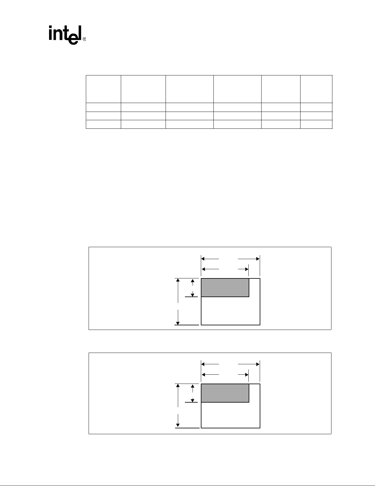
®
Intel
Celeron® Processor up to 1.10 GHz
T a ble 41. Intel® Celeron® Processor for the FC-PGA2 Package Thermal Design Power 1
Processor
900 900 100 30.0 72 5
950 950 100 32.0 72 5
1 GHz 1000 100 33.9 69 5
NOTES:
1. These values are specified at nominal VCC
2. Thermal Design Powe r (TDP) represents the maximum amount of power the thermal solution is required to
dissipate. The thermal solution should be designed to dissipate the TDP power without exceeding the
maximum Tc ase specification.
3. TDP does not represent the power delivery and voltage regulation requirements for the processor. Refer to
Table 5 for voltage regulation and electrical specifications.
4. T
CaseOffset
temperature on the processor’s core. For more information refer to the document,
Processor in the FC-PGA2 Package Thermal Design Guide.
5. This processor exi sts in both FC-PGA and FC-PGA2 packages.
Processor Core
Frequency (MHz)
is the worst-case difference between the maximum case temperature and the thermal diode
System Bus
Frequency (MHz)
for the processor pins.
CORE
Processor
Thermal Design
CPUID 068Ah (W)
Power
2,3
Maximum
4
(°C)
T
case
Intel® Pentium® III
Additional
Notes
Figure 17 is a block diagram of the Intel Celeron FC-PGA/FC-PGA2 processor die layout. The
layout differentiates the processor core from the cache die area. In ef fect, the thermal desi gn power
identified in Table 40 is dissipated entirely from the processor core area. Thermal solution designs
should compensate for this smaller heat flux area and not assume that the power is uniformly
distributed across the entire die area.
Figure 17. Processor Functional Die Layout (CPUID 0686h)
(1)
0.337”
0.275”
Die Area = 0.90 cm
Cache Area = 0.26 cm
Core Area = 0.64 cm
2
2
2
0.146”
Cache Area
0.04 in
0.414” Core Area
0.10 in
1. For CPUID 0x68A, the die area is 0.94 cm2, the cache area is 0.30 cm2, and the core area is 0.64 cm2.
Figure 18. Processor Functional Die Layout (up to CPUID 0683h)
0.362”
0.292”
Die Area = 1.05 cm
Cache Area = 0.32 cm
Core Area = 0.73 cm
2
2
2
0.170”
0.448”
Cache Area
0.05 in
Core Area
0.11 in
2
2
2
2
Die Area
0.14 in
Die Area
0.16 in
2
2
Datasheet 67
Page 68
®
Intel
Celeron® Processor up to 1.10 GHz
4.1.1 Thermal Diode
The Celeron processor incorporates an on-die diode that can be used to monitor the die
temperature. A thermal sensor located on the motherboard or a standalone measurement kit may
monitor the die temperature of the Intel Celeron processor for thermal management purposes.
Table 42 to Tabl e 44 provide the diode parameter and interface specifications.
Note: The reading of the thermal sensor connected to the thermal diode will not necessarily reflect the
temperature of the hottest location on the die. This is due to inaccuracies in the thermal sensor, ondie temperature gradients between the location of the thermal diode and the hottest location on the
die at a given point in time, and time based variations in the die temperature measurement. Time
based variations can occur when the sampling rate of the thermal diode (by the thermal sensor) is
slower than the rate at which the T
Table 42. Thermal Diode Parameters (S.E.P. and PPGA Packages)
Symbol Min Typ Max Unit Notes
I
forward bias
n_ideality 1.0000 1.0065 1.0173 2,3
NOTES:
1. Intel does not support or recommend operation of the thermal diode under reverse bias.
2. At room temperature wi th a forward bias of 630 mV.
3. n _ideality is the diode ideality factor parameter, as represented by the diode equation:
I-Io(e (Vd*q)/(nkT) – 1).
4. N ot 100% tested. Specified by design characterization.
5 500 uA 1
temperature can change.
junction
Table 43. Thermal Diode Parameters (FC-PGA/FC-PGA2 Packages)
Symbol Min Typ Max Unit Notes
I
forward bias
n_ideality 1.0057 1.0080 1.0125 2, 3
NOTES:
1. Intel does not support or recommend operation of the thermal diode under reverse bias.
2. C haract eri zed at 100° C with a forward bias current of 5–300 µA.
3. The ideality fac tor, n, represents the deviation from ideal diode behavior as exemplified by the diode
equation:
=Is(e^ ((Vd*q)/(nkT)) – 1), where Is = saturation current, q = electronic charge, Vd = voltage across the
I
fw
diode, k = Boltzmann Constant, and T = absolute temperature (Kelvin).
4. N ot 100% tested. Specified by design characterization.
5 300 uA 1
Table 44. Thermal Diode Interface
Pin Name
THERMDP B14 AL31 diode anode (p junction)
THERMDN B15 AL29 diode cathode (n junction)
SC242 Connector
Signal #
370-Pin Socket Pin # Pin Description
68 Datasheet
Page 69

5.0 Mechanical Specifications
There are three package technologies which Celeron processors use. They are the S.E.P. Package,
the PPGA package, and the FC-PGA/FC-PGA2 packages. The S.E.P. Package and FC-PGA/
FC-PGA2 packages contain the processor core and passive components, while the PPGA package
does not have passive components.
The processor edge connector defined in this document is referred to as the “SC242 connector.”
See the SC242 Design Guidelines (Order Number 243397) for further details on the edge
connector.
The processor socket connector is defined in this document is referred to as the “370-pin socket.”
See the 370-Pin Socket (PGA370) Design Guidelines (Ord er Number 244410 ) for furth er details on
the socket.
5.1 S.E.P. Package
This section defines the mechanical specifications and signal definitions for the Celeron processor
in the S.E.P. Package.
®
Intel
Celeron® Processor up to 1.10 GHz
5.1.1 Materials Information
The Celeron processor requires a retention mechanism. This retention mechanism may require
motherboard holes to be 0.159" diameter if low cost plastic fasteners are used to secure the
retention mechanisms. The larger diameter holes are ne cessary to provide a r obust structural design
that can shock and vibe testing. If captive nuts are used in place of the plas tic fastener s, then either
the 0.159" or the 0.140" diameter holes will suffice as long as the attach mount is used.
Figure 19 with substrate dimensions is provided to aid in the design of a heatsink and clip. In
Figure 20 all area on the secondary side of the substrate is zoned “keepout”, except for 25 mils
around the tooling holes and the top and side edges of the substrate.
Datasheet 69
Page 70
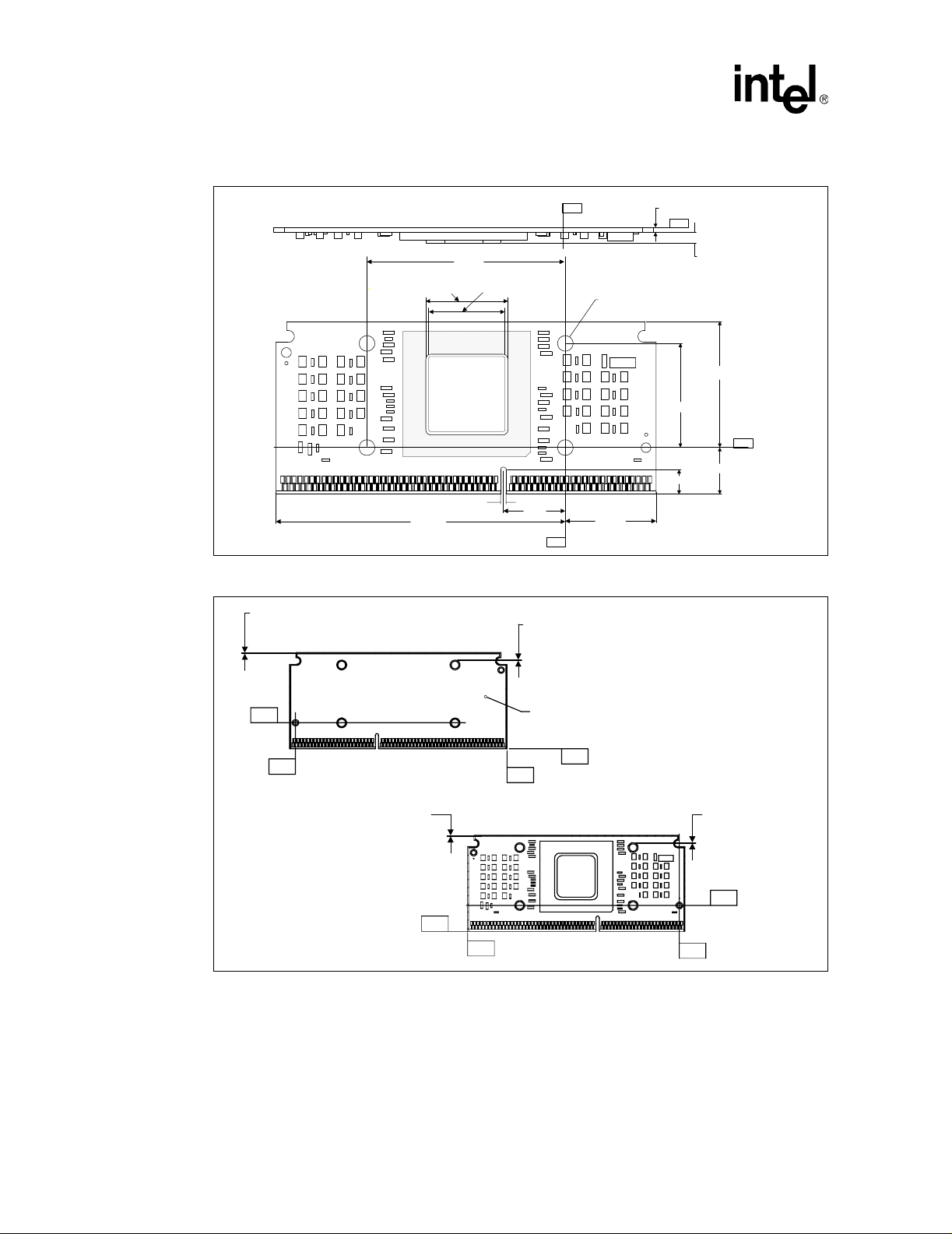
®
e
Intel
Celeron® Processor up to 1.10 GHz
Figure 19. Processor Substrate Dimensions (S.E.P. Package)
+.007
-Y-
.062
-.005
-Z-
3.804
2.608
25.4 mm Copper
Slug Square
.814
1.660
1.370
-Y-
.615
.323
1.196
-Y-
27.4 mm SR
Opening Square
Figure 20. Processor Substrate Primary/Secondary Side Dimensions (S.E.P. Package)
Typ Max.
.025
Non-Keepout Area
-D-
Secondary Side
Typ Max.
.025
Non-Keepout Area
There Will be No Components on
Secodonary Side
-E-
Typ Max.
.025
Non-Keepout Area
-H-
-G-
-H-
-G-
Primary Side
.025
Non-Keepout Ar
-D-
-E-
Typ Max.
5.1.2 Signal Listing (S.E.P. Package)
Table 45 and Table 46 provide the processor edge finger and SC242 connector signal definitions
for Celeron processor. The signal locations on the SC242 edge connector are to be used for signal
routing, simulation, and component placement on the motherboard.
70 Datasheet
Page 71
®
Intel
Celeron® Processor up to 1.10 GHz
T able 45. S.E.P . Package Signal Listing
by Pin Number
Pin
No. Pin Name Signal Buffer Type
A1 VTT Power/Other
A2 V
A3 V
A4 IERR# CMOS Output
A5 A 20M# CMOS Input
A6 V
A7 FERR# CMOS Output
A8 I G NNE# CMOS Input
A9 TDI T A P Input
A10 V
A1 1 TDO TAP Outp u t
A12 PWRGOOD CMOS Input
A13 TESTHI CMOS Test Input
A14 V
A15 THERMTRIP# CMOS Output
A16 Reserved Reserved for Future Use
A17 LINT0/INTR CMOS Input
A18 V
A19 PICD0 APIC I/O
A20 PREQ# CMOS Input
A21 BP3# AGTL+ I/O
A22 V
A23 BPM0# AGTL+ I/O
A24 Reserved
A25 Reserved
A26 V
A27 Reserved
A28 Reserved
A29 Reserved
A30 V
A31 Reserved
A32 D61# AGTL+ I/O
A33 D55# AGTL+ I/O
A34 V
SS Power/Other
TT Power/Other
SS Power/Other
SS Power/Other
SS Power/Other
SS Power/Other
SS Power/Other
Reserved for Pentium
processor
Reserved for Pentium
processor
SS Power/Other
Reserved for Pentium
processor
Reserved for Pentium
processor
Reserved for Pentium
processor
SS Power/Other
Reserved for Pentium
processor
SS Power/Other
II
II
II
II
II
II
T able 45. S.E.P . Package Signal Listing
by Pin Number
Pin
No. Pin Name Signal Buffer Type
A35 D60# AGTL+ I/O
A36 D53# AGTL+ I/O
A37 D57# AGTL+ I/O
A38 V
A39 D46# AGTL+ I/O
A40 D49# AGTL+ I/O
A41 D51# AGTL+ I/O
A42 V
A43 D42# AGTL+ I/O
A44 D45# AGTL+ I/O
A45 D39# AGTL+ I/O
A46 V
A47 Reserved Reserved for Future Use
A48 D43# AGTL+ I/O
A49 D37# AGTL+ I/O
A50 V
A51 D33# AGTL+ I/O
A52 D35# AGTL+ I/O
A53 D31# AGTL+ I/O
A54 V
A55 D30# AGTL+ I/O
A56 D27# AGTL+ I/O
A57 D24# AGTL+ I/O
A58 V
A59 D23# AGTL+ I/O
A60 D21# AGTL+ I/O
A61 D16# AGTL+ I/O
A62 V
A63 D13# AGTL+ I/O
A64 D11# AGTL+ I/O
A65 D10# AGTL+ I/O
A66 V
A67 D14# AGTL+ I/O
A68 D9# AGTL+ I/O
A69 D8# AGTL+ I/O
A70 V
A71 D5# AGTL+ I/O
SS Power/Other
SS Power/Other
SS Power/Other
SS Power/Other
SS Power/Other
SS Power/Other
SS Power/Other
SS Power/Other
SS Power/Other
Datasheet 71
Page 72
®
Intel
Celeron® Processor up to 1.10 GHz
Table 45. S.E.P . Package Signal Listing
by Pin Number
Pin
No. Pin Name Signal Buffer Type
A72 D3# AGTL+ I/O
A73 D1# AGTL+ I/O
A74 V
A75 BCLK System Bus Clock Input
A76 Reserved
A77 Reserved
A78 V
A79 Reserved
A80 Reserved
A81 A30# AGTL+ I/O
A82 V
A83 A31# AGTL+ I/O
A84 A27# AGTL+ I/O
A85 A22# AGTL+ I/O
A86 V
A87 A23# AGTL+ I/O
A88 Reserved Reserved for Future Use
A89 A19# AGTL+ I/O
A90 V
A91 A18# AGTL+ I/O
A92 A16# AGTL+ I/O
A93 A13# AGTL+ I/O
A94 V
A95 A14# AGTL+ I/O
A96 A10# AGTL+ I/O
A97 A5# AGTL+ I/O
A98 V
A99 A9# AGTL+ I/O
A100 A4# AGTL+ I/O
A101 BNR# AGTL+ I/O
A102 V
A103 BPRI# AGTL+ Input
A104 TRDY# AGTL+ Input
A105 DEFER# AGTL+ Input
A106 V
SS Power/Other
Reserved for Pentium
processor
Reserved for Pentium
processor
SS Power/Other
Reserved for Pentium
processor
Reserved for Pentium
processor
SS Power/Other
SS Power/Other
SS Power/Other
SS Power/Other
SS Power/Other
SS Power/Other
SS Power/Other
II
II
II
II
T able 45. S.E.P . Package Signal Listing
by Pin Number
Pin
No. Pin Name Signal Buffer Type
A107 REQ2# AGTL+ I/O
A108 REQ3# AGTL+ I/O
A109 HITM# AGTL+ I/O
A110 V
A111 DBSY# AGTL+ I/O
A112 RS1# AGTL+ Input
A113 Reserved Reserved for Future Use
A114 V
A115 ADS# AGTL+ I/O
A116 Reserved Reserved for Future Use
A117 Reserved
A118 V
A119 VID2 Power/Other
A120 VID1 Power/Other
A121 VID4 Power/Other
B1 EMI Power/Other
B2 FLUSH# CMOS Input
B3 SMI# CMOS Input
B4 INIT# CMOS Input
B5 V
B6 STPCLK# CMOS Input
B7 TCK TAP Input
B8 SLP# CMOS Input
B9 V
B10 TMS T AP Input
B13 V
B14 THERMDP Power/Other
B15 THERMDN Power/Other
B16 LINT1/NMI CMOS Input
B17 V
B18 PICCLK APIC Clock Input
B19 BP2# A GTL+ I/O
B20 Reserved Reserved for Future Use
B21 BSEL Power/Other
B22 PICD1 APIC I/O
B23 PRDY# AGTL+ Output
B24 BPM1# AGTL+ I/O
SS Power/Other
SS Power/Other
Reserved for Pentium
processor
SS Power/Other
TT Power/Other
TT Power/Other
CC
CC
CORE
CORE
Power/Other
Power/Other
II
72 Datasheet
Page 73
®
Intel
Celeron® Processor up to 1.10 GHz
T able 45. S.E.P . Package Signal Listing
by Pin Number
Pin
No. Pin Name Signal Buffer Type
B25 VCC
CORE
B26 Reserved
B27 Reserved
B28 Reserved
B29 V
CC
CORE
B30 D62# AGTL+ I/O
B31 D58# AGTL+ I/O
B32 D63# AGTL+ I/O
B33 V
CC
CORE
B34 D56# AGTL+ I/O
B35 D50# AGTL+ I/O
B36 D54# AGTL+ I/O
B37 V
CC
CORE
B38 D59# AGTL+ I/O
B39 D48# AGTL+ I/O
B40 D52# AGTL+ I/O
B41 EMI Power/Other
B42 D41# AGTL+ I/O
B43 D47# AGTL+ I/O
B44 D44# AGTL+ I/O
B45 V
CC
CORE
B46 D36# AGTL+ I/O
B47 D40# AGTL+ I/O
B48 D34# AGTL+ I/O
B49 V
CC
CORE
B50 D38# AGTL+ I/O
B51 D32# AGTL+ I/O
B52 D28# AGTL+ I/O
B53 V
CC
CORE
B54 D29# AGTL+ I/O
B55 D26# AGTL+ I/O
B56 D25# AGTL+ I/O
B57 V
CC
CORE
B58 D22# AGTL+ I/O
B59 D19# AGTL+ I/O
B60 D18# AGTL+ I/O
Power/Other
Reserved for Pentium
processor
Reserved for Pentium
processor
Reserved for Pentium
processor
Power/Other
Power/Other
Power/Other
Power/Other
Power/Other
Power/Other
Power/Other
II
II
II
T able 45. S.E.P . Package Signal Listing
by Pin Number
Pin
No. Pin Name Signal Buffer Type
B61 EMI Power/Other
B62 D20# AGTL+ I/O
B63 D17# AGTL+ I/O
B64 D15# AGTL+ I/O
B65 V
B66 D12# AGTL+ I/O
B67 D7# AGTL+ I/O
B68 D6# AGTL+ I/O
B69 V
B70 D4# AGTL+ I/O
B71 D2# AGTL+ I/O
B72 D0# AGTL+ I/O
B73 V
B74 RESET# AGTL+ Input
B75 Reserved Reserved for Future Use
B76 Reserved Reserved for Future Use
B77 V
B78 Reserved
B79 Reserved
B80 A29# AGTL+ I/O
B81 EMI Power/Other
B82 A26# AGTL+ I/O
B83 A24# AGTL+ I/O
B84 A28# AGTL+ I/O
B85 V
B86 A20# AGTL+ I/O
B87 A21# AGTL+ I/O
B88 A25# AGTL+ I/O
B89 V
B90 A15# AGTL+ I/O
B91 A17# AGTL+ I/O
B92 A11# AGTL+ I/O
B93 V
B94 A12# AGTL+ I/O
B95 A8# AGTL+ I/O
B96 A7# AGTL+ I/O
CC
CC
CC
CC
CC
CC
CC
CORE
CORE
CORE
CORE
CORE
CORE
CORE
Power/Other
Power/Other
Power/Other
Power/Other
Reserved for Pentium
processor
Reserved for Pentium
processor
Power/Other
Power/Other
Power/Other
II
II
Datasheet 73
Page 74

®
Intel
Celeron® Processor up to 1.10 GHz
Table 45. S.E.P . Package Signal Listing
by Pin Number
Pin
No. Pin Name Signal Buffer Type
B97 VCC
CORE
B98 A3# AGTL+ I/O
B99 A6# AGTL+ I/O
B100 EMI Power/Other
B101 SLOTOCC# Power/Other
B102 REQ0# AGTL+ I/O
B103 REQ1# AGTL+ I/O
B104 REQ4# AGTL+ I/O
B105 V
CC
CORE
B106 LOCK# AGTL+ I/O
B107 DRDY# AGTL+ I/O
B108 RS0# AGTL+ Input
B109 V
CC
5
B11 T RST# TAP Input
B110 HIT# AG TL+ I/O
B111 RS2# AGTL+ Input
Power/Other
Power/Other
Power/Other
T able 45. S.E.P . Package Signal Listing
by Pin Number
Pin
No. Pin Name Signal Buffer Type
B112 Reserved Reserved for Future Use
B113 V
CC
L2
B114 Reserved
B115 Reserved
B116 Reserved
B117 V
CC
L2
B118 Reserved
B119 VID3 Power/Other
B12 Reserved Reserved for Future Use
B120 VID0 Power/Other
B121 V
CC
L2
Power/Other. Reserved
for Pentium
II processor
Reserved for Pentium
processor
Reserved for Pentium
processor
Reserved for Pentium
processor
Power/Other. Reserved
for Pentium II processor
Reserved for Pentium
processor
Power/Other. Reserved
for Pentium
II processor
II
II
II
II
74 Datasheet
Page 75

®
Intel
Celeron® Processor up to 1.10 GHz
T able 46. S.E.P . Package Signal Listing
by Signal Name
Pin Name
A3# B98 AGTL + I/O
A4# A100 AGTL+ I/O
A5# A97 AGTL + I/O
A6# B99 AGTL + I/O
A7# B96 AGTL + I/O
A8# B95 AGTL + I/O
A9# A99 AGTL + I/O
A10# A96 AGTL+ I/O
A11# B92 AGTL+ I/O
A12# B94 AGTL+ I/O
A13# A93 AGTL+ I/O
A14# A95 AGTL+ I/O
A15# B90 AGTL+ I/O
A16# A92 AGTL+ I/O
A17# B91 AGTL+ I/O
A18# A91 AGTL+ I/O
A19# A89 AGTL+ I/O
A20# B86 AGTL+ I/O
A20M# A5 CMOS Input
A21# B87 AGTL+ I/O
A22# A85 AGTL+ I/O
A23# A87 AGTL+ I/O
A24# B83 AGTL+ I/O
A25# B88 AGTL+ I/O
A26# B82 AGTL+ I/O
A27# A84 AGTL+ I/O
A28# B84 AGTL+ I/O
A29# B80 AGTL+ I/O
A30# A81 AGTL+ I/O
A31# A83 AGTL+ I/O
ADS# A115 AGTL+ I/O
BCLK A75 System Bus Clock Input
BNR# A101 AGTL+ I/O
BP2# B19 AG TL+ I/O
BP3# A21 AG TL+ I/O
BPM0# A23 AG TL + I/ O
BPM1# B24 AG TL + I/ O
Pin
No. Signal Buffer Type
T able 46. S.E.P . Package Signal Listing
by Signal Name
Pin Name
BPRI# A103 AGTL+ Input
BSEL B21 Power/Other
D00# B72 AGTL+ I/O
D1# A73 AGTL+ I/O
D2# B71 AGTL+ I/O
D3# A72 AGTL+ I/O
D5# A71 AGTL+ I/O
D6# B68 AGTL+ I/O
D7# B67 AGTL+ I/O
D8# A69 AGTL+ I/O
D9# A68 AGTL+ I/O
D10# A65 AGTL+ I/O
D11# A64 AGTL+ I/O
D12# B66 AGTL+ I/O
D13# A63 AGTL+ I/O
D14# A67 AGTL+ I/O
D15# B64 AGTL+ I/O
D16# A61 AGTL+ I/O
D17# B63 AGTL+ I/O
D18# B60 AGTL+ I/O
D19# B59 AGTL+ I/O
D20# B62 AGTL+ I/O
D21# A60 AGTL+ I/O
D22# B58 AGTL+ I/O
D23# A59 AGTL+ I/O
D24# A57 AGTL+ I/O
D25# B56 AGTL+ I/O
D26# B55 AGTL+ I/O
D27# A56 AGTL+ I/O
D28# B52 AGTL+ I/O
D29# B54 AGTL+ I/O
D30# A55 AGTL+ I/O
D31# A53 AGTL+ I/O
D32# B51 AGTL+ I/O
D33# A51 AGTL+ I/O
D34# B48 AGTL+ I/O
D35# A52 AGTL+ I/O
Pin
No. Signal Buffer Type
Datasheet 75
Page 76

®
Intel
Celeron® Processor up to 1.10 GHz
Table 46. S.E.P . Package Signal Listing
by Signal Name
Pin Name
D36# B46 AGTL+ I/O
D37# A49 AGTL+ I/O
D38# B50 AGTL+ I/O
D39# A45 AGTL+ I/O
D4# B70 AGTL+ I/O
D40# B47 AGTL+ I/O
D41# B42 AGTL+ I/O
D42# A43 AGTL+ I/O
D43# A48 AGTL+ I/O
D44# B44 AGTL+ I/O
D45# A44 AGTL+ I/O
D46# A39 AGTL+ I/O
D47# B43 AGTL+ I/O
D48# B39 AGTL+ I/O
D49# A40 AGTL+ I/O
D50# B35 AGTL+ I/O
D51# A41 AGTL+ I/O
D52# B40 AGTL+ I/O
D53# A36 AGTL+ I/O
D54# B36 AGTL+ I/O
D55# A33 AGTL+ I/O
D56# B34 AGTL+ I/O
D57# A37 AGTL+ I/O
D58# B31 AGTL+ I/O
D59# B38 AGTL+ I/O
D60# A35 AGTL+ I/O
D61# A32 AGTL+ I/O
D62# B30 AGTL+ I/O
D63# B32 AGTL+ I/O
DBSY# A111 AGTL+ I/O
DEFER# A105 AGTL+ Input
DRDY# B107 AGTL+ I/O
EMI B1 Power/Other
EMI B41 Power/Other
EMI B61 Power/Other
EMI B81 Power/Other
EMI B100 Power/Other
Pin
No. Signal Buffer Type
T able 46. S.E.P . Package Signal Listing
by Signal Name
Pin Name
FERR# A7 CMOS Output
FLUSH# B2 CMOS Input
HIT# B110 AGTL+ I/O
HITM# A109 AG TL+ I/O
IERR# A4 CMOS Output
IGNNE# A8 CMOS Input
INIT# B4 CMOS Input
LINT0/INTR A17 CMOS Input
LINT1/NMI B16 CMOS Input
LOCK# B106 AGTL+ I/O
PICCLK B18 APIC Clock Input
PICD0 A19 APIC I/O
PICD1 B22 APIC I/O
PRDY# B23 AGTL+ Output
PREQ# A20 CMOS Input
PWRGOOD A12 CMOS Input
REQ0# B102 AGTL+ I/O
REQ1# B103 AGTL+ I/O
REQ2# A107 AGTL+ I/O
REQ3# A108 AGTL+ I/O
REQ4# B104 AGTL+ I/O
Reserved A16 Reserved for Future Use
Reserved A47 Reserved for Future Use
Reserved A77
Reserved A88 Reserved for Future Use
Reserved A116 Reserved for Future Use
Reserved B12 Reserved for Future Use
Reserved A113 Reserved for Future Use
Reserved B20 Reserved for Future Use
Reserved B76 Reserved for Future Use
Reserved B112 Reserved for Future Use
Reserved B79
Reserved B114
Reserved B115
Pin
No. Signal Buffer Type
Reserved for Pentium
processor
Reserved for Pentium
processor
Reserved for Pentium
processor
Reserved for Pentium
processor
II
II
II
II
76 Datasheet
Page 77

®
Intel
Celeron® Processor up to 1.10 GHz
T able 46. S.E.P . Package Signal Listing
by Signal Name
Pin Name
Reserved A117
Reserved B116
Reserved A24
Reserved A76
Reserved B75 Reserved for Future Use
Reserved A79
Reserved A80
Reserved B78
Reserved B118
Reserved A25
Reserved A27
Reserved B26
Reserved A28
Reserved B27
Reserved A29
Reserved A31
Reserved B28
RESET# B74 AGTL+ Input
RS0# B108 AGTL+ Input
RS1# A112 AGTL+ Input
RS2# B11 1 AGTL+ Input
SLOTOCC# B101 Power/Other
SLP# B8 CMOS Input
SMI# B3 CMOS Input
STPCLK# B6 CMOS Input
TCK B7 TAP Input
TDI A9 TAP Input
TDO A11 TAP Output
Pin
No. Signal Buffer Type
Reserved for Pentium
processor
Reserved for Pentium
processor
Reserved for Pentium
processor
Reserved for Pentium
processor
Reserved for Pentium
processor
Reserved for Pentium
processor
Reserved for Pentium
processor
Reserved for Pentium
processor
Reserved for Pentium
processor
Reserved for Pentium
processor
Reserved for Pentium
processor
Reserved for Pentium
processor
Reserved for Pentium
processor
Reserved for Pentium
processor
Reserved for Pentium
processor
Reserved for Pentium
processor
II
II
II
II
II
II
II
II
II
II
II
II
II
II
II
II
T able 46. S.E.P . Package Signal Listing
by Signal Name
Pin Name
TESTHI A13 CMOS Test Input
THERMDN B15 Power/Other
THERMDP B14 Power/Other
THERMTRIP# A15 CMOS Output
TMS B10 TAP Input
TRDY# A104 AGTL+ Input
TRST# B11 TAP Input
V
CC
5
V
CC
CORE
V
CC
CORE
V
CC
CORE
V
CC
CORE
V
CC
CORE
V
CC
CORE
V
CC
CORE
V
CC
CORE
V
CC
CORE
V
CC
CORE
V
CC
CORE
V
CC
CORE
V
CC
CORE
V
CC
CORE
V
CC
CORE
V
CC
CORE
V
CC
CORE
V
CC
CORE
V
CC
CORE
V
CC
L2
V
CC
L2
V
CC
L2
VID0 B120 Power/Other
VID1 A120 Power/Other
VID2 A119 Power/Other
VID3 B119 Power/Other
VID4 A121 Power/Other
V
SS A114 Power/Other
Pin
No. Signal Buffer Type
B109 Power/Other
B13 Power/Other
B17 Power/Other
B25 Power/Other
B29 Power/Other
B33 Power/Other
B37 Power/Other
B45 Power/Other
B49 Power/Other
B53 Power/Other
B57 Power/Other
B65 Power/Other
B69 Power/Other
B73 Power/Other
B77 Power/Other
B85 Power/Other
B89 Power/Other
B93 Power/Other
B97 Power/Other
B105 Power/Other
Power/Other. Reserved
B113
for Pentium
Power/Other. Reserved
B117
for Pentium
Power/Other. Reserved
B121
for Pentium
II processor
II processor
II processor
Datasheet 77
Page 78

®
Intel
Celeron® Processor up to 1.10 GHz
Table 46. S.E.P . Package Signal Listing
by Signal Name
Pin Name
VSS A118 Power/Other
V
SS A46 Power/Other
SS A38 Power/Other
V
V
SS A42 Power/Other
SS A50 Power/Other
V
V
SS A54 Power/Other
SS A58 Power/Other
V
V
SS A62 Power/Other
V
SS A66 Power/Other
V
SS A70 Power/Other
V
SS A74 Power/Other
V
SS A78 Power/Other
V
SS A82 Power/Other
V
SS A86 Power/Other
V
SS A2 Power/Other
V
SS A6 Power/Other
Pin
No. Signal Buffer Type
T able 46. S.E.P . Package Signal Listing
by Signal Name
Pin Name
VSS A10 Power/Other
V
SS A14 Power/Other
SS A18 Power/Other
V
V
SS A22 Power/Other
SS A26 Power/Other
V
V
SS A30 Power/Other
SS A34 Power/Other
V
V
SS A98 Power/Other
V
SS A102 Power/Other
V
SS A106 Power/Other
V
SS A110 Power/Other
V
TT A1 Power/Other
V
TT A3 Power/Other
V
TT B5 Power/Other
V
TT B9 Power/Other
Pin
No. Signal Buffer Type
78 Datasheet
Page 79

Intel
5.2 PPGA Package
This section defines the mechanical specifications and signal definitions for the Celeron processor
in the PPGA packages.
5.2.1 PPGA Package Materials Information
Figure 21 and Table 47 are provided to aid in the design of a heatsink and clip.
Figure 21. Package Dimensions (PPGA Package)
®
Celeron® Processor up to 1.10 GHz
45° x 0.085
Bottom View
D
D1
Seating Plane
A1
L
S1
D
Side View
D2
Top View
Heat Slug Solder Resist
B1 B2
A
A2
e1
φ
B
Datasheet 79
Page 80
®
Intel
Celeron® Processor up to 1.10 GHz
T able 47. Package Dimensions (PPGA Package)
Millimeters Inches
Symbol Min Max Notes Min Max Notes
A 1.83 2.23 0.072 0.088
A1 1.00 0.039
A2 2.72 3.33 0.107 0.131
B 0.40 0.51 0.016 0.020
D 49.43 49.63 1.946 1.954
D1 45.59 45.85 1.795 1.805
D2 25.15 25.65 0.099 1.010
e1 2.29 2.79 0.090 0.110
L 3.05 3.30 0.120 0.130
N 370 Lead Count 370 Lead Count
S1 1.52 2.54 0.060 0.100
T a ble 48. Information Summary (PPGA Package)
Package Type Total Pins Pin Array Package Size
Plastic Staggered Pin Grid Array (PPGA) 370 37 x 37
1.95" x 1.95"
4.95 cm x 4.95 cm
80 Datasheet
Page 81

5.2.2 PPGA Package Signal Listing
Figure 22. PPGA Package (Pin Side View)
1 2 3 4 5 6 7 8 9 10111213141516171819202122 2324252627282930313233 34353637
®
Intel
Celeron® Processor up to 1.10 GHz
AN
AM
AL
AK
AJ
AH
AG
AF
AE
AD
AC
AB
AA
Z
Y
X
W
V
U
T
S
R
Q
P
N
M
L
K
J
H
G
F
E
D
C
B
A
VSS A12# A6# Rsvd Rsvd Rsvd BPRI# DEFER# Rsvd Rsvd TRDY# DRDY# BR0# ADS# TRST# TDI TDO
VSS VCC VSS VCC VSS VCC VSS
VSS A15# A9# Rsvd Rsvd
VSS
VCC VSS A28# A3#
A21# VSS VCC VSS VCC VSS VCC VSS VCC VSS VCC VSS VCC VSS
VSS Rsvd A10# A5#
EDGCTRL A19# VSS
VCC Rsvd A25#
A17# A22#
VSS
Rsvd A20# VSS
VCC
A27# A30# VCC
VSS A29#
Rsvd A26# VSS
RESET#
Rsvd
D0# Rsvd VCC
VSS Rsvd
D15# VSS
D4#
VCC D1# D6#
D8# D5#
Rsvd D17# VREF3
D12# D10#
VCC D18# D9#
D2# D14# VCC
VSS
D13#
D20# VSS
VCC VREF2 D24#
D7#
D30#
VSS D16# D19#
D23#
D21#
VCC VCC D32# D22# Rsvd D27#
D25#
D26#
VSS
VCC
D33#
D35#
D29#
1 2 3 4 5 6 7 8 9 10111213141516171819202122 2324252627282930313233 34353637
VCC
VREF5
A31#
A24#
A18#
VCC
VSS
D11# D3#
VCC
VSS
VCC
VSS
VCC
D31#
VSS
VCC VSS
D28#
A23#
Rsvd
VREF4
A16#
A13#
A11# VREF6 A14# Rsvd REQ0# LOCK#
A8#
A4# BNR# REQ1# REQ2# Rsvd RS1# VCC RS0# THERMTRIP# SLP#
VSS
D34#
D43#
VCC
D38#
D36#
D37# D44#
D39#
VCC
VCC D63# VREF1 VSS VCC VSS VCC VSS VCC VSS
VCC VSS
VSS
D41#
D42#
D49#
D45#
VSS
D51#
VCC VSS
A7#
REQ4# REQ3#
VCC VSS
D52#
D40# D59# D55#
VCC
VSS
D47# D48#
VCC VSS
Rsvd
VREF7
CORE
V
VSS
VCC
DET
VCC VSS VCC VSS
D54# D58# D50#
VSS VCC VSS VCC
D57#
D46# D53#
VCC
HITM#
Rsvd PWRGD
Rsvd
VSS VCC VSS
HIT#
DBSY# THRMDN THRMDP TCK VID0 VID2
RS2#
D62# Rsvd
VCC
D56#
VSS VCC VSS VCC
D61#
D60#
VCC
Rsvd TMS
VCC VSS
VCC
VSS
VCC
VSS
VCC VSS
VSS VCC
VCC VSS VCC
VSS
VCC VSS VCC
VSS VCC VSS
VCC VSS LINT0
VCC VCC VSS
PICCLK
VCC VSS VCC
Rsvd
Rsvd
VSS VCC VSS VCC
Rsvd Rsvd BPM0#
Rsvd
Rsvd Rsvd
VSS VID1
VCC
VSS
SMI# VID3
BSEL#
VSS VCC
STPCLK# IGNNE#
INIT#
VCC VSS
A20M# IERR# FLUSH#
VSS
V1.5
VSS
FERR# Rsvd
VCMOS
VCC
Rsvd Rsvd VCC
V2.5
VSS VCC VSS
VSS
PLL1 Rsvd
PLL2
Rsvd Rsvd Rsvd
Rsvd
Rsvd
Rsvd PICD1
BP2# Rsvd Rsvd
VREF0 BPM1#
Rsvd PRDY#
Rsvd Rsvd
VCC VSS
Rsvd
Rsvd
PICD0
VCC VSS
Rsvd
BCLK
Rsvd
Rsvd
LINT1
PREQ#
BP3#
CPUPRES#
VSS
AN
AM
AL
AK
AJ
AH
AG
AF
AE
AD
AC
AB
AA
Z
Y
X
W
V
U
T
S
R
Q
P
N
M
L
K
J
H
G
F
E
D
C
B
A
Datasheet 81
Page 82
®
Intel
Celeron® Processor up to 1.10 GHz
T able 49. PPGA Package Signal Listing
by Pin Number
Pin
No. Pin Name Signal Buffer Type
A3 D29 # AGTL+ I/O
A5 D28 # AGTL+ I/O
A7 D43 # AGTL+ I/O
A9 D37 # AGTL+ I/O
A11 D44# AGTL+ I/O
A13 D51# AGTL+ I/O
A15 D47# AGTL+ I/O
A17 D48# AGTL+ I/O
A19 D57# AGTL+ I/O
A21 D46# AGTL+ I/O
A23 D53# AGTL+ I/O
A25 D60# AGTL+ I/O
A27 D61# AGTL+ I/O
A29 Reserved Reserved for Future Use
A31 Reserved Reserved for Future Use
A33 Reserved Reserved for Future Use
A35 PRDY# AGTL+ Output
A37 V
AA1 A27# AGTL+ I/O
AA3 A30# AGTL+ I/O
AA5 V
AA33 Reserved Reserved for Future Use
AA35 Reserved Reserved for Future Use
AA37 V
AB2 V
AB4 A24# AGTL+ I/O
AB6 A23# AGTL+ I/O
AB32 V
AB34 V
AB36 V
AC1 Reserved Reserved for Future Use
AC3 A20# AGTL+ I/O
AC5 V
AC33 V
AC35 FERR# CMOS Output
AC37 Reserv ed Reserved for Future Use
AD2 V
SS Power/Other
CC
CORE
CC
CORE
CC
CORE
SS Power/Other
CC
CORE
CC
CMOS
SS Power/Other
SS Power/Other
SS Power/Other
Power/Other
Power/Other
Power/Other
Power/Other
Power/Other
T able 49. PPGA Package Signal Listing
by Pin Number
Pin
No. Pin Name Signal Buffer Type
AD4 A31# AGTL+ I/O
AD6 V
AD32 V
AD34 V
AD36 V
AE1 A17# AGTL+ I/O
AE3 A22# AGTL+ I/O
AE5 V
AE33 A20M# CMOS Input
AE35 IERR# CMOS Output
AE37 FLUSH# CMOS Input
AF2 V
AF4 Reserved Reserved for Future Use
AF6 A25# AGTL+ I/O
AF32 V
AF34 V
AF36 V
AG1 EDGCTRL Power/Other
AG3 A19# AGTL+ I/O
AG5 V
AG33 INIT# CMOS Input
AG35 STPCLK# CMOS Input
AG37 IGNNE# CMOS Input
AH2 V
AH4 Reserved Reserved for Future Use
AH6 A10# AGTL+ I/O
AH8 A5# AGTL+ I/O
AH10 A8# AGTL+ I/O
AH12 A4# AGTL+ I/O
AH14 BNR# A GTL+ I/O
AH16 REQ1# AGTL+ I/O
AH18 REQ2# AGTL+ I/O
AH20 Reserved Reserved for Future Use
AH22 RS1# AGTL+ Input
AH24 V
AH26 RS0# AGTL+ Input
AH28 THERMTRIP# CMOS Output
AH30 SLP# CMOS Input
REF
5
CC
CORE
SS Power/Other
CC
1.5
CC
CORE
CC
CORE
SS Power/Other
CC
CORE
SS Power/Other
SS Power/Other
SS Power/Other
CC
CORE
Power/Other
Power/Other
Power/Other
Power/Other
Power/Other
Power/Other
Power/Other
82 Datasheet
Page 83
®
Intel
Celeron® Processor up to 1.10 GHz
T able 49. PPGA Package Signal Listing
by Pin Number
Pin
No. Pin Name S ignal Buffer Type
AH32 VCC
AH34 V
AH36 V
CORE
SS Power/Other
CC
CORE
AJ01 A21# AGTL+ I/O
AJ03 V
AJ05 V
AJ07 V
AJ09 V
AJ11 V
AJ13 V
AJ15 V
AJ17 V
AJ19 V
AJ21 V
AJ23 V
AJ25 V
AJ27 V
AJ29 V
AJ31 V
SS Power/Other
CC
CORE
SS Power/Other
CC
CORE
SS Power/Other
CC
CORE
SS Power/Other
CC
CORE
SS Power/Other
CC
CORE
SS Power/Other
CC
CORE
SS Power/Other
CC
CORE
SS Power/Other
AJ33 BSEL Power/Other
AJ35 SMI# CMOS Input
AJ37 VID3 Power/Other
AK02 V
AK04 V
CC
CORE
SS Power/Other
AK06 A28# AGTL+ I/O
AK08 A3# AGTL+ I/O
AK10 A11# AGTL+ I/O
AK12 V
REF6 Power/Other
AK14 A14# AGTL+ I/O
AK16 Reserved Reserved for Future Use
AK18 REQ0# AGTL+ I/O
AK20 LOCK# AGTL+ I/O
AK22 V
REF7 Power/Other
AK24 Reserved Reserved for Future Use
AK26 PWRGOOD CMOS Input
AK28 RS2# AGTL+ Input
AK30 Reserved Reserved for Future Use
AK32 TMS TAP Input
Power/Other
Power/Other
Power/Other
Power/Other
Power/Other
Power/Other
Power/Other
Power/Other
Power/Other
Power/Other
Table 49. PPGA Package Signal Listing
by Pin Number
Pin
No. Pin Name Signal Buffer Type
AK34 VCC
AK36 V
AL01 V
AL03 V
CORE
SS Power/Other
SS Power/Other
SS Power/Other
AL05 A15# AGTL+ I/O
AL07 A13# AGTL+ I/O
AL09 A9# AGTL+ I/O
AL11 Reserved Reserved for Future Use
AL13 Reserved Reserved for Future Use
AL15 A7# AGTL+ I/O
AL17 REQ4# AGTL+ I/O
AL19 REQ3# AGTL+ I/O
AL21 Reserved Reserved for Future Use
AL23 HITM# AGTL+ I/O
AL25 HIT# AGTL+ I/O
AL27 DBSY# AGTL+ I/O
AL29 THERMDN Power/Other
AL31 THERMDP Power/Other
AL33 TCK TAP Input
AL35 VID0 Voltage Identification
AL37 VID2 Voltage Identification
AM04 V
AM06 V
AM08 V
AM10 V
AM12 V
AM14 V
AM16 V
AM18 V
AM2 V
AM20 V
AM22 V
AM24 V
AM26 V
AM28 V
AM30 V
AM32 V
AM34 V
CC
CORE
SS Power/Other
CC
CORE
SS Power/Other
CC
CORE
SS Power/Other
CC
CORE
SS Power/Other
SS Power/Other
CC
CORE
SS Power/Other
CC
CORE
SS Power/Other
CC
CORE
SS Power/Other
CC
CORE
SS Power/Other
Power/Other
Power/Other
Power/Other
Power/Other
Power/Other
Power/Other
Power/Other
Power/Other
Power/Other
Datasheet 83
Page 84
®
Intel
Celeron® Processor up to 1.10 GHz
T able 49. PPGA Package Signal Listing
by Pin Number
Pin
No. Pin Name Signal Buffer Type
AM36 VID1 Voltage Identification
AN3 V
AN5 A12# AGTL+ I/O
AN7 A16# AGTL+ I/O
AN9 A6# AGTL+ I/O
AN11 Reserv ed Reserved for Future Use
AN13 Reserv ed Reserved for Future Use
AN15 Reserv ed Reserved for Future Use
AN17 BPRI# AGTL+ Input
AN19 DEFER# AGTL+ Input
AN21 Reserv ed Reserved for Future Use
AN23 Reserv ed Reserved for Future Use
AN25 TRDY# AGTL+ Input
AN27 DRDY# AGTL+ I/O
AN29 BR0# AGTL+ I/O
AN31 A DS# AGTL+ I/O
AN33 TRST# TAP Input
AN35 TDI TAP Input
AN37 TDO TAP Output
B2 D35 # AGTL+ I/O
B4 V
B6 V
B8 V
B10 V
B12 V
B14 V
B16 V
B18 V
B20 V
B22 V
B24 V
B26 V
B28 V
B30 V
B32 V
B34 V
B36 Reserved Reserved for Future Use
C1 D 33# AGTL+ I/O
SS Power/Other
SS Power/Other
CC
CORE
SS Power/Other
CC
CORE
SS Power/Other
CC
CORE
SS Power/Other
CC
CORE
SS Power/Other
CC
CORE
SS Power/Other
CC
CORE
SS Power/Other
CC
CORE
SS Power/Other
CC
CORE
Power/Other
Power/Other
Power/Other
Power/Other
Power/Other
Power/Other
Power/Other
Power/Other
T able 49. PPGA Package Signal Listing
by Pin Number
Pin
No. Pin Name Signal Buffer Type
C3 VCC
CORE
C5 D31# AGTL+ I/O
C7 D34# AGTL+ I/O
C9 D36# AGTL+ I/O
C11 D45# AGTL+ I/O
C13 D49# AGTL+ I/O
C15 D40# AGTL+ I/O
C17 D59# AGTL+ I/O
C19 D55# AGTL+ I/O
C21 D54# AGTL+ I/O
C23 D58# AGTL+ I/O
C25 D50# AGTL+ I/O
C27 D56# AGTL+ I/O
C29 Reserved Reserved for Future Use
C31 Reserved Reserved for Future Use
C33 Reserved Reserved for Future Use
C35 BPM0# AGTL+ I/O
C37 CPUPRES# Power/Other
D2 V
D4 V
D6 V
SS Power/Other
SS Power/Other
CC
CORE
D8 D38# AGTL+ I/O
D10 D39# AGTL+ I/O
D12 D42# AGTL+ I/O
D14 D41# AGTL+ I/O
D16 D52# AGTL+ I/O
D18 V
D20 V
D22 V
D24 V
D26 V
D28 V
D30 V
D32 V
D34 V
D36 V
SS Power/Other
CC
CORE
SS Power/Other
CC
CORE
SS Power/Other
CC
CORE
SS Power/Other
CC
CORE
SS Power/Other
CC
CORE
E1 D26# AGTL+ I/O
E3 D25# AGTL+ I/O
Power/Other
Power/Other
Power/Other
Power/Other
Power/Other
Power/Other
Power/Other
84 Datasheet
Page 85

®
Intel
Celeron® Processor up to 1.10 GHz
T able 49. PPGA Package Signal Listing
by Pin Number
Pin
No. Pin Name S ignal Buffer Type
E5 VCC
E7 V
E9 V
E11 V
E13 V
E15 V
E17 V
E19 V
E21 V
CORE
SS Power/Other
CC
CORE
SS Power/Other
CC
CORE
SS Power/Other
CC
CORE
SS Power/Other
CORE
DET
E23 Reserved Reserved for Future Use
E25 D62# Power/Other
E27 Reserved Reserved for Future Use
E29 Reserved Reserved for Future Use
E31 Reserved Reserved for Future Use
E33 V
REF0 Power/Other
E35 BPM1# AGTL+ I/O
E37 BP3# AGTL+ I/O
F2 V
F4 V
CC
CC
CORE
CORE
F6 D32# A GTL+ I/O
F8 D22# A GTL+ I/O
F10 Reserved Reserved for Future Use
F12 D27# AGTL+ I/O
F14 V
CC
CORE
F16 D63# AGTL+ I/O
F18 V
F20 V
F22 V
F24 V
F26 V
F28 V
F30 V
F32 V
F34 V
F36 V
REF1 Power/Other
SS Power/Other
CC
CORE
SS Power/Other
CC
CORE
SS Power/Other
CC
CORE
SS Power/Other
CC
CORE
SS Power/Other
G1 D21# AGTL+ I/O
G3 D23# AGTL+ I/O
G5 V
SS Power/Other
Power/Other
Power/Other
Power/Other
Power/Other
Power/Other
Power/Other
Power/Other
Power/Other
Power/Other
Power/Other
Power/Other
Power/Other
Table 49. PPGA Package Signal Listing
by Pin Number
Pin
No. Pin Name Signal Buffer Type
G33 BP2# AGTL+ I/O
G35 Reserved Reserved for Future Use
G37 Reserved Reserved for Future Use
H2 V
H4 D16# AGTL+ I/O
H6 D19# AGTL+ I/O
H32 V
H34 V
H36 V
J1 D7# AGTL+ I/O
J3 D30# AGTL+ I/O
J5 V
J33 PICCLK APIC Clock Input
J35 PICD0 APIC I/O
J37 PREQ# CMOS Input
K2 V
K4 V
K6 D24# AG TL+ I/O
K32 V
K34 V
K36 V
L1 D13# AGTL+ I/O
L3 D20# AGTL+ I/O
L5 V
L33 Reserved Reserved for Future Use
L35 PICD1 APIC I/O
L37 LINT1/NM I CMOS Input
M2 V
M4 D11# AGTL+ I/O
M6 D3# AGTL+ I/O
M32 V
M34 V
M36 LINT0/INTR CMOS Input
N1 D2# AG TL+ I/O
N3 D14# AGTL+ I/O
N5 V
N33 Reserved Reserved for Future Use
N35 Reserved Reserved for Future Use
SS Power/Other
CC
CORE
SS Power/Other
CC
CORE
CC
CORE
CC
CORE
REF2 Power/Other
CC
CORE
CC
CORE
SS Power/Other
SS Power/Other
SS Power/Other
CC
CORE
SS Power/Other
CC
CORE
Power/Other
Power/Other
Power/Other
Power/Other
Power/Other
Power/Other
Power/Other
Power/Other
Datasheet 85
Page 86
®
Intel
Celeron® Processor up to 1.10 GHz
T able 49. PPGA Package Signal Listing
by Pin Number
Pin
No. Pin Name Signal Buffer Type
N37 Reserved Reserved for Future Use
P2 V
CC
CORE
P4 D18 # AGTL+ I/O
P6 D9# AGTL+ I/O
P32 V
P34 V
P36 V
SS Power/Other
CC
CORE
SS Power/Other
Q1 D12# AGTL+ I/ O
Q3 D10# AGTL+ I/ O
Q5 V
SS Power/Other
Q33 Reserved Reserved for Future Use
Q35 Reserved Reserved for Future Use
Q37 Reserved Reserved for Future Use
R2 Reserved Reserved for Future Use
R4 D 17# AGTL+ I/O
R6 V
R32 V
R34 V
R36 V
REF3 Power/Other
CC
CORE
SS Power/Other
CC
CORE
S1 D8# AGTL+ I/O
S3 D5# AGTL+ I/O
S5 V
CC
CORE
S33 Reserved Reserved for Future Use
S35 Reserved Reserved for Future Use
S37 Reserved Reserved for Future Use
T2 V
CC
CORE
T4 D1# AGTL+ I/O
T6 D6# AGTL+ I/O
T32 V
T34 V
T36 V
SS Power/Other
CC
CORE
SS Power/Other
U1 D4# AGTL+ I/O
U3 D 15# AGTL+ I/O
Power/Other
Power/Other
Power/Other
Power/Other
Power/Other
Power/Other
Power/Other
T able 49. PPGA Package Signal Listing
by Pin Number
Pin
No. Pin Name Signal Buffer Type
U5 VSS Power/Other
U33 PLL2 Power/Other
U35 Reserved Reserved for Future Use
U37 Reserved Reserved for Future Use
V2 V
V4 Reserved Reserved for Future Use
V6 V
V32 V
V34 V
V36 V
W1 D0# AGTL+ I/O
W3 Reserved Reserved for Future Use
W5 V
W33 PLL1 Power/Other
W35 Reserved Reserved for Future Use
W37 BCLK System Bus Clock Input
X2 Reserved Reserved for Future Use
X4 RESET# AGTL+ Input
X6 Reserved Reserved for Future Use
X32 V
X34 V
X36 V
Y1 Reserved Reserved for Future Use
Y3 A26# AGTL+ I/O
Y5 V
Y33 V
Y35 V
Y37 V
Z2 V
Z4 A29# AGTL+ I/O
Z6 A18# AGTL+ I/O
Z32 V
Z34 V
Z36 V
SS Power/Other
REF4 Power/Other
CC
CORE
SS Power/Other
CC
CORE
CC
CORE
SS Power/Other
CC
CORE
SS Power/Other
SS Power/Other
SS Power/Other
CC
CORE
SS Power/Other
SS Power/Other
CC
CORE
SS Power/Other
CC
2.5
Power/Other
Power/Other
Power/Other
Power/Other
Power/Other
Power/Other
Power/Other
86 Datasheet
Page 87
®
Intel
Celeron® Processor up to 1.10 GHz
T able 50. PPGA Package Signal Listing
in Order by Signal Name
Pin Name
A3# AK8 AGTL+ I/O
A4# AH12 AGTL+ I/O
A5# AH8 AGTL+ I/O
A6# AN9 AGTL+ I/O
A7# AL15 AGTL+ I/O
A8# AH10 AGTL+ I/O
A9# AL9 AGTL+ I/O
A10# AH6 AGTL+ I/O
A11# AK10 AGTL+ I/O
A12# AN5 AGTL+ I/O
A13# AL7 AGTL+ I/O
A14# AK14 AGTL+ I/O
A15# AL5 AGTL+ I/O
A16# AN7 AGTL+ I/O
A17# AE1 AGTL+ I/O
A18# Z6 AGTL+ I/O
A19# AG3 AGTL+ I/O
A20# AC3 AGTL+ I/O
A21# AJ1 AGTL+ I/O
A22# AE3 AGTL+ I/O
A23# AB6 AGTL+ I/O
A24# AB4 AGTL+ I/O
A25# AF6 AGTL+ I/O
A26# Y3 AGTL+ I/O
A27# AA1 AGTL+ I/O
A28# AK6 AGTL+ I/O
A29# Z4 AGTL+ I/O
A30# AA3 AGTL+ I/O
A31# AD4 AGTL+ I/O
A20M# A E33 CMOS Input
ADS# AN31 AGTL+ I/O
BCLK W37 System Bus Clock Input
BNR# AH14 AGTL+ I/O
BP2# G33 AGTL+ I/O
BP3# E37 AGTL+ I/O
BPM0# C35 AGTL+ I/O
BPM1# E35 AGTL+ I/O
BPRI# AN17 AGTL+ Input
BR0# AN29 AGTL+ I/O
BSEL AJ33 Power/Other
Pin
No. Signal Buffer Type
Table 50. PPGA Package Signal Listing
in Order by Signal Name
Pin Name
CPUPRES# C37 Power/Other
D0# W1 A GTL+ I/O
D1# T4 AGTL+ I/O
D2# N1 AGTL+ I/O
D3# M6 AGTL+ I/O
D4# U1 AGTL+ I/O
D5# S3 AGTL+ I/O
D6# T6 AGTL+ I/O
D7# J1 AGTL+ I/O
D8# S1 AGTL+ I/O
D9# P6 AGTL+ I/O
D10# Q3 AGTL+ I/O
D11# M4 AGTL+ I/O
D12# Q1 AGTL+ I/O
D13# L1 AGTL+ I/O
D14# N3 AGTL+ I/O
D15# U3 AGTL+ I/O
D16# H4 AGTL+ I/O
D17# R4 AGTL+ I/O
D18# P4 AGTL+ I/O
D19# H6 AGTL+ I/O
D20# L3 AGTL+ I/O
D21# G1 AGTL+ I/O
D22# F8 AGTL+ I/O
D23# G3 AGTL+ I/O
D24# K6 AGTL+ I/O
D25# E3 AGTL+ I/O
D26# E1 AGTL+ I/O
D27# F12 A GTL+ I/O
D28# A5 AGTL+ I/O
D29# A3 AGTL+ I/O
D30# J3 AGTL+ I/O
D31# C5 AGTL+ I/O
D32# F6 AGTL+ I/O
D33# C1 AGTL+ I/O
D34# C7 AGTL+ I/O
D35# B2 AGTL+ I/O
D36# C9 AGTL+ I/O
D37# A9 AGTL+ I/O
D38# D8 AGTL+ I/O
Pin
No. Signal Buffer Type
Datasheet 87
Page 88
®
Intel
Celeron® Processor up to 1.10 GHz
T able 50. PPGA Package Signal Listing
in Order by Signal Name
Pin Name
D39# D10 AGTL+ I/O
D40# C15 AGTL+ I/O
D41# D14 AGTL+ I/O
D42# D12 AGTL+ I/O
D43# A7 AGTL+ I/O
D44# A11 AGTL+ I/O
D45# C11 AGTL+ I/O
D46# A21 AGTL+ I/O
D47# A15 AGTL+ I/O
D48# A17 AGTL+ I/O
D49# C13 AGTL+ I/O
D50# C25 AGTL+ I/O
D51# A13 AGTL+ I/O
D52# D16 AGTL+ I/O
D53# A23 AGTL+ I/O
D54# C21 AGTL+ I/O
D55# C19 AGTL+ I/O
D56# C27 AGTL+ I/O
D57# A19 AGTL+ I/O
D58# C23 AGTL+ I/O
D59# C17 AGTL+ I/O
D60# A25 AGTL+ I/O
D61# A27 AGTL+ I/O
D62# E25 AGTL+ I/O
D63# F16 AGTL+ I/O
DBSY# AL27 AGTL+ I/O
DEFER# AN19 AGTL+ Input
DRDY# AN27 AGTL+ I/O
EDGCTRL AG1 Power/Other
FERR# AC35 CMOS Output
FLUSH# AE37 CMOS Input
HIT# AL25 AGTL+ I/O
HITM# AL23 AG TL+ I/ O
IERR# AE35 CMOS Output
IGNNE# AG37 CMOS Input
INIT# AG33 CMOS Input
LINT0/INTR M36 CMOS Input
LINT1/NMI L37 CMOS Input
LOCK# AK20 AGTL+ I/O
PICCLK J33 APIC Clock Input
Pin
No. Signal Buffer Type
T able 50. PPGA Package Signal Listing
in Order by Sign al Name
Pin Name
PICD0 J35 APIC I/O
PICD1 L35 APIC I/O
PLL1 W33 Power/Other
PLL2 U33 Power/Other
PRDY# A35 AGTL+ Output
PREQ# J37 CMOS Input
PWRGOOD AK26 CMOS Input
REQ0# AK18 AGTL+ I/O
REQ1# AH16 AGTL+ I/O
REQ2# AH18 AGTL+ I/O
REQ3# AL19 AGTL+ I/O
REQ4# AL17 AGTL+ I/O
Reserved AC1 Reserved for Future Use
Reserved AC37 Reserved for Future Use
Reserved AF4 Reserved for Future Use
Reserved AK16 Reserved for Future Use
Reserved AK24 Reserved for Future Use
Reserved AK30 Reserved for Future Use
Reserved AL11 Reserved for Future Use
Reserved AL13 Reserved for Future Use
Reserved AL21 Reserved for Future Use
Reserved AN11 Reserved for Future Use
Reserved AN13 Reserved for Future Use
Reserved AN15 Reserved for Future Use
Reserved AN21 Reserved for Future Use
Reserved AN23 Reserved for Future Use
Reserved B36 Reserved for Future Use
Reserved C29 Reserved for Future Use
Reserved C31 Reserved for Future Use
Reserved C33 Reserved for Future Use
Reserved E23 Reserved for Future Use
Reserved E29 Reserved for Future Use
Reserved E31 Reserved for Future Use
Reserved F10 Reserved for Future Use
Reserved G35 Reserved for Future Use
Reserved G37 Reserved for Future Use
Reserved L33 Reserved for Future Use
Reserved N33 Reserved for Future Use
Reserved N35 Reserved for Future Use
Reserved N37 Reserved for Future Use
Pin
No. Signal Buffer Type
88 Datasheet
Page 89
®
Intel
Celeron® Processor up to 1.10 GHz
T able 50. PPGA Package Signal Listing
in Order by Signal Name
Pin Name
Reserved Q33 Reserved for Future Use
Reserved Q35 Reserved for Future Use
Reserved Q37 Reserved for Future Use
Reserved S33 Reserved for Future Use
Reserved S37 Reserved for Future Use
Reserved U35 R eserved for Future Use
Reserved U37 R eserved for Future Use
Reserved V4 Reserved for Future Use
Reserved W3 Reserved for Future Use
Reserved W35 Reserved for Future Use
Reserved AH20 Reserved for Future Use
Reserved AH4 Reserved for Future Use
Reserved A29 Reserved for Future Use
Reserved A31 Reserved for Future Use
Reserved A33 Reserved for Future Use
Reserved AA33 Reserved for Future Use
Reserved AA35 Reserved for Future Use
Reserved X6 Reserved for Future Use
Reserved Y1 Reserved for Future Use
Reserved E27 Reserved for Future Use
Reserved R2 Reserved for Future Use
Reserved S35 Reserved for Future Use
Reserved X2 Reserved for Future Use
RESET# X4 AGTL+ Input
RS0# AH26 AGTL+ Input
RS1# AH22 AGTL+ Input
RS2# AK28 AGTL+ Input
SLP# AH30 CMOS Input
SMI# AJ35 CMOS Input
STPCLK# AG35 CMOS Input
TCK AL33 TAP Input
TDI AN35 TAP Input
TDO AN37 T A P Output
THERMDN AL29 Power/Other
THERMDP AL31 Power/Other
THERMTRIP# AH28 CMOS Output
TMS AK32 TAP Input
TRDY# AN25 AGTL+ Input
TRST# AN33 TAP Input
CC
V
1.5
Pin
No. Signal Buffer Type
AD36 Power/Other
Table 50. PPGA Package Signal Listing
in Order by Signal Name
Pin Name
VCC
2.5
CC
V
CMOS
CC
V
CORE
V
CC
CORE
CC
V
CORE
CC
V
CORE
V
CC
CORE
CC
V
CORE
CC
V
CORE
V
CC
CORE
CC
V
CORE
CC
V
CORE
V
CC
CORE
CC
V
CORE
CC
V
CORE
CC
V
CORE
CC
V
CORE
CC
V
CORE
V
CC
CORE
CC
V
CORE
CC
V
CORE
CC
V
CORE
CC
V
CORE
CC
V
CORE
CC
V
CORE
CC
V
CORE
CC
V
CORE
V
CC
CORE
CC
V
CORE
CC
V
CORE
V
CC
CORE
CC
V
CORE
CC
V
CORE
CC
V
CORE
V
CC
CORE
CC
V
CORE
CC
V
CORE
CC
V
CORE
CC
V
CORE
CC
V
CORE
Pin
No. Signal Buffer Type
Z36 Power/Other
AB36 Power/Other
AJ25 Power/Other
AJ29 Power/Other
AJ5 Power/Other
AJ9 Power/Other
AK2 Power/Other
AK34 Power/Other
AM12 Power/Other
AM16 Power/Other
AM20 Power/Other
AM24 Power/Other
AM28 Power/Other
AM32 Power/Other
AM4 Power/Other
AM8 Power/Other
B10 Power/Other
B14 Power/Other
B18 Power/Other
B22 Power/Other
B26 Power/Other
B30 Power/Other
B34 Power/Other
B6 Power/Other
C3 Power/Other
D20 Power/Other
D24 Power/Other
D28 Power/Other
D32 Power/Other
D36 Power/Other
D6 Power/Other
E13 Power/Other
E17 Power/Other
E5 Power/Other
E9 Power/Other
F14 Power/Other
F2 Power/Other
F22 Power/Other
F26 Power/Other
AA37 Power/Other
Datasheet 89
Page 90

®
Intel
Celeron® Processor up to 1.10 GHz
T able 50. PPGA Package Signal Listing
in Order by Signal Name
Pin Name
VCC
CORE
CC
V
CORE
CC
V
CORE
V
CC
CORE
CC
V
CORE
CC
V
CORE
V
CC
CORE
CC
V
CORE
CC
V
CORE
V
CC
CORE
CC
V
CORE
CC
V
CORE
V
CC
CORE
CC
V
CORE
CC
V
CORE
CC
V
CORE
CC
V
CORE
CC
V
CORE
V
CC
CORE
CC
V
CORE
CC
V
CORE
CC
V
CORE
CC
V
CORE
CC
V
CORE
CC
V
CORE
CC
V
CORE
CC
V
CORE
V
CC
CORE
CC
V
CORE
CC
V
CORE
V
CC
CORE
CC
V
CORE
CC
V
CORE
CC
V
CORE
V
CC
CORE
CC
V
CORE
CC
V
CORE
CORE
V
DET
VID0 AL35 Power/Other
VID1 AM36 Power/Other
Pin
No. Signal Buffer Type
AA5 Power/Other
AB2 Power/Other
AB34 Power/Other
AD32 Power/Other
AE5 Power/Other
AF2 Power/Other
AF34 Power/Other
AH24 Power/Other
AH32 Power/Other
AH36 Power/Other
AJ13 Power/Other
AJ17 Power/Other
AJ21 Power/Other
F30 Power/Other
F34 Power/Other
F4 Power/Other
H32 Power/Other
H36 Power/Other
J5 Power/Other
K2 Power/Other
K32 Power/Other
K34 Power/Other
M32 Power/Other
N5 Power/Other
P2 Power/Other
P34 Power/Other
R32 Power/Other
R36 Power/Other
S5 Power/Other
T2 Power/Other
T34 Power/Other
V32 Power/Other
V36 Power/Other
W5 Power/Other
X34 Power/Other
Y35 Power/Other
Z32 Power/Other
E21 Power/Other
T able 50. PPGA Package Signal Listing
in Order by Sign al Name
Pin Name
VID2 AL37 Power/Other
VID3 AJ37 Power/Other
REF0 E33 Power/Other
V
V
REF1 F18 Power/Other
REF2 K4 Power/Other
V
REF3 R6 Power/Other
V
V
REF4 V6 Power/Other
REF5 AD6 Power/Other
V
REF6 AK12 Power/Other
V
V
REF7 AK22 Power/Other
SS B16 Power/Other
V
SS B20 Power/Other
V
V
SS B24 Power/Other
SS B28 Power/Other
V
SS B32 Power/Other
V
SS B4 Power/Other
V
SS B8 Power/Other
V
SS D18 Power/Other
V
V
SS D2 Power/Other
SS D22 Power/Other
V
SS D26 Power/Other
V
SS D30 Power/Other
V
SS D34 Power/Other
V
SS D4 Power/Other
V
SS E11 Power/Other
V
SS E15 Power/Other
V
SS E19 Power/Other
V
V
SS E7 Power/Other
SS F20 Power/Other
V
SS F24 Power/Other
V
V
SS F28 Power/Other
SS F32 Power/Other
V
SS F36 Power/Other
V
SS G5 Power/Other
V
V
SS H2 Power/Other
SS H34 Power/Other
V
SS K36 Power/Other
V
SS L5 Power/Other
V
SS M2 Power/Other
V
SS M34 Power/Other
V
Pin
No. Signal Buffer Type
90 Datasheet
Page 91

®
Intel
Celeron® Processor up to 1.10 GHz
T able 50. PPGA Package Signal Listing
in Order by Signal Name
Pin Name
VSS P32 Power/Other
SS P36 Power/Other
V
SS Q5 Power/Other
V
V
SS R34 Power/Other
SS T32 Power/Other
V
SS T36 Power/Other
V
V
SS U5 Power/Other
SS V2 Power/Other
V
SS A37 Power/Other
V
V
SS AB32 Power/Other
SS AC33 Power/Other
V
SS AC5 Power/Other
V
V
SS AD2 Power/Other
SS AD34 Power/Other
V
SS AF32 Power/Other
V
SS AF36 Power/Other
V
SS AG5 Power/Other
V
SS AH2 Power/Other
V
V
SS AH34 Power/Other
SS AJ11 Power/Other
V
SS AJ15 Power/Other
V
SS AJ19 Power/Other
V
SS AJ23 Power/Other
V
SS AJ27 Power/Other
V
SS AJ3 Power/Other
V
Pin
No. Signal Buffer Type
Table 50. PPGA Package Signal Listing
in Order by Signal Name
Pin Name
VSS AJ7 Power/Other
SS AK36 Power/Other
V
SS AK4 Power/Other
V
V
SS AL1 Power/Other
SS AL3 Power/Other
V
SS AM10 Power/Other
V
V
SS AM14 Power/Other
SS AM18 Power/Other
V
SS AM2 Power/Other
V
V
SS AM22 Power/Other
SS AM26 Power/Other
V
SS AM30 Power/Other
V
V
SS AM34 Power/Other
SS AM6 Power/Other
V
SS AN3 Power/Other
V
SS B12 Power/Other
V
SS V34 Power/Other
V
SS X32 Power/Other
V
V
SS X36 Power/Other
SS Y37 Power/Other
V
SS Y5 Power/Other
V
SS Z2 Power/Other
V
SS Z34 Power/Other
V
SS AJ31 Power/Other
V
SS Y33 Power/Other
V
Pin
No. Signal Buffer Type
Datasheet 91
Page 92

®
Intel
Celeron® Processor up to 1.10 GHz
5.3 FC-PGA/FC-PGA2 Packages
This section defines the mechanical specifications and signal definitions for the Intel Celeron
processor in the FC-PGA and FC-PGA2 packages.
5.3.1 FC-PGA Mechanical Specifications
Figure 23 is provided to aid in the design of heatsink and clip solutions as well as demonstrate
where pin-side capacitors will be located on the processor. Table 51 provides the measurements for
these dimensions in both inches and millimeters.
Figure 23. Package Dimensions (FC-PGA Package)
NOTES:
1. Unless otherwise specified, the following drawings are dimensioned in inches.
2. Al l dimensi ons provi ded with tolerances are guaranteed to be met for all normal production product.
3. Figures and drawings labeled as “Reference Dimensions” are provided for informational purposes only.
Reference dimensions are extracted from the mechanical design database and are nominal dimensions with
no tolerance information applied. Reference dimensions are NOT checked as part of the processor
manufacturing. Unless noted as such, dimensions in parentheses without tolerances are reference
dimensions.
4. Drawing not to scale.
92 Datasheet
Page 93

T a ble 51. Package Dimensions (FC-PGA Package)
Millimeters Inches
Symbol Min Max Notes Min Max Notes
A1 0.787 0.889 0.031 0.035
A2 1.000 1.200 0.039 0.047
B1 11.183 11.285 0.440 0.445
B2 9.225 9.327 0.363 0.368
C1 23.495 max 0.925 max
C2 21.590 max 0.850 max
D 49.428 49.632 1.946 1.954
D1 45.466 45.947 1.790 1.810
G1 0.000 17.780 1 0.000 0.700
G2 0.000 17.780 1 0.000 0.700
G3 0.000 0.889 1 0.000 0.035
H 2.540 Nominal 0.100 Nominal
L 3.048 3.302 0.120 0.130
ϕP 0.431 0.483 0.017 0.019
Pin TP 0.508 Diametric True Position (Pin-to-Pin) 0.020 Diametric True Position (Pin-to-Pin)
®
Intel
Celeron® Processor up to 1.10 GHz
NOTES:
1. Capacitors and resist ors may be placed on the pin-side of the FC-PGA package in the area defined by G1,
G2, and G3. This area is a keepout zone for motherboard designers.
The bare processor die has mechanical load limits that should not be exceeded during heatsink
assembly, mechanical stress testing, or standard drop and shipping conditions. The heatsink attach
solution must not induce permanent stress into the processor substrate with the exception of a
uniform load to maintain the heatsink to the proces sor thermal interfac e. The package dynamic an d
static loading parameters are listed in Table 52.
For Table 52, the following apply:
1. It is not recommended to use any portion of the processor substrate as a mechanical reference
or load bearing surface for thermal solutions.
2. Parameters assume uniformly applied loads
T a ble 52. Processor Die Loading Parameters (FC-PGA Package)
Parameter Dynamic (max)1Static (max)
Silicon Die Surface 200 50 lbf
Silicon Die Edge 100 12 lbf
NOTES:
1. This specif icati on applies to a uniform and a non-uniform load.
2. This is the maximum static force that can be applied by the heatsink and clip to maintain the heatsink and
processor interface.
2
Unit
Datasheet 93
Page 94

®
Intel
Celeron® Processor up to 1.10 GHz
5.3.2 Mechanical Specifications (FC-PGA2 Package)
Figure 24 is provided to aid in the design of heatsink and clip solutions as well as demonstrate
where pin-side capacitors will be located on the processor. Table 53 lists the measurements for
these dimensions in both inches and millimeters.
Figure 24. Package Dimensions (FC-PGA2 Package)
94 Datasheet
Page 95

T able 53. Package Dimensions (FC-PGA2 Package)
®
Intel
Celeron® Processor up to 1.10 GHz
Symbol
Minimum Maximum Notes Minimum Maximum Notes
A1 2.266 2.690 0.089 0.106
A2 0.980 1.180 0.038 0.047
B1 30.800 31.200 1.212 1.229
B2 30.800 31.200 1.212 1.229
C1 33.000 max 1.299 max
C2 33.000 max 1.299 max
D 49.428 49.632 1.946 1.954
D1 45.466 45.974 1.790 1.810
G1 0.000 17.780 0.000 0.700
G2 0.000 17.780 0.000 0.700
G3 0.000 0.889 0.000 0.035
H 2.540 Nominal 0.100 Nominal
L 3.048 3.302 0.120 0.130
ΦP 0.431 0.483 0.017 0.019
Pin TP 0.508 Diametric True Position (Pin-to-Pin) 0.020 Diametric True Position (Pin-to-Pin)
NOTE: Capacitors will be placed on the pin-side of the FC-PGA2 package in the area defined by G1, G2, and
G3. This area is a keepout zone for motherboard designers.
Millimeters Inches
For Table 52, the following apply:
1. It is not recommended to use any portion of the processor substrate as a mechanical reference
or load bearing surface for thermal solutions.
2. Parameters assume uniformly applied loads.
T able 54. Processor Case Loading Parameters (FC-PGA2 Package)
Parameter Dynamic (max)1Static (max)
IHS Surface 200 100 lbf
IHS Edge 125 N/A lbf
IHS Corner 75 N/A ibf
NOTES:
1. This specif icati on applies to a uniform and a non-uniform load.
2. This is the maximum static force that can be applied by the heatsink and clip to maintain the heatsink and
processor interface.
3. See socket manufa ctur er’s force loading specification also to ensure compliance. Maximum static loading
listed here does not account for the maximum reaction forces on the socket tabs or pins.
2,3
Unit
Datasheet 95
Page 96
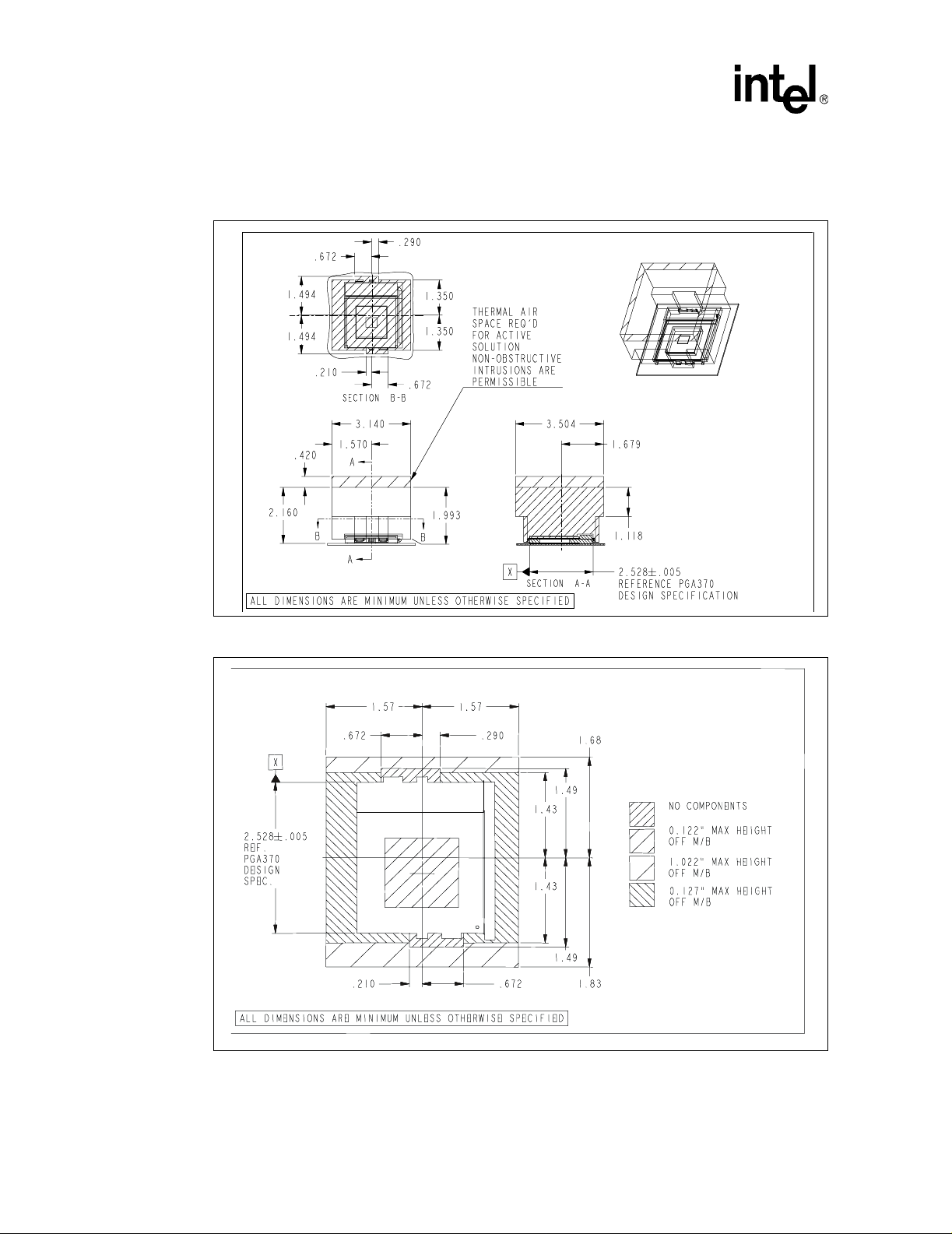
®
Intel
Celeron® Processor up to 1.10 GHz
5.3.2.1 Recommended Mechanical Keep-Out Zones (FC-PGA2 Package)
Figure 25. Volumetric Keep-Out
Figure 26. Component Keep-Out
96 Datasheet
Page 97

Intel
5.3.3 FC-PGA/FC-PGA2 Package Signal List
Figure 27. Package Dimensions (FC-PGA/FC-PGA2 Packages)
1 2 3 4 5 6 7 8 9 10111213141516171819202122 2324252627282930313233 34353637
®
Celeron® Processor up to 1.10 GHz
AN
AM
AL
AK
AJ
AH
AG
AF
AE
AD
AC
AB
AA
VSS
RSV
VSS VSS A15 A13 A9 RSV
VCC VSS A28 A3
A21 VSS VCC VSS VCC VSS VCC VSS VCC VSS VCC VSS VCC VSS VCC BSEL1 BSEL0 SMI VID3
VSS RSV A10 A5 A8 A4 BNR REQ1 REQ2 RSV RS1 VCC RS0
A19 VSS
EDGCTRL
VCC
A17 A22
VSS A31 VREF5
RSV A20 VSS
VCC
A27 A30 VCC
Z
VSS A29 A18
Y
RSV
X
W
V
U
T
S
R
Q
P
N
M
L
K
J
H
G
F
E
D
C
B
A
A26 VSS
RSV RESET RSV
D0
RSV
VSS
D4 D15 VSS
VCC D1 D6
D8 D5 VCC
RSV D17
D12
D10
VCC D18 D9
D2 D14 VCC
VSS
D13 D20 VSS
VCC VREF2 D24
D7
D30
VSS
D21 D23
VCC VCC D32 D22 RSV D27
D26
D25
VSS
VCC
D33
D29
1 2 3 4 5 6 7 8 9 10111213141516171819202122 23 2425262728293031323334353637
A16 A6
A12
VCC VSS VCC VSS VCC VSS
A25
RSV
VCC
A24
A23
VCC
RSV VREF4
VREF3
VSS
D11 D3
VCC
D16
D19
VSS
VCC
VSS
VCC
D31
D34
VSSD35
VCC
D28
D43
VSS
RSV RSV
RSV
VREF6 A14 RSV REQ0
A11
VCCVSS
D38
D39
D36
VCC
D37
VCC D63
VSS
VCC VSS VCC VSS RSV RSV D62
D41 D52 VSS VCC VSS VCC VSS VCC VSS VCC VSS VCC
D42
D45 D49
VSS
D44
D51 D47 D48 D57 D46 D53 D60 D61 RSV RSV RSV PRDY VSS
RSV BPRI DEFER RSV RSV TRDY DRDY BR0 ADS TRST TDI TDO
VSS VCC
VCC
A7 REQ4 REQ3 RSV HITM HIT DBSY THRMDN THRMDP TCK VID0 VID2
LOCK
PIN SIDE VIEW
VSS VCC VSS VCC VSS
VREF1
D40 D59 D55 D54 D58 D50 D56 RSV RSV RSV BPM0
VCC VSS
VCC
VSS VCC VSS VCC VSS VCC VSS VCC RSV
VCC VSS VCC
VSS
VREF7 RSV
VSS
RS2 RSV TMS VCC VSS
PWRGD
SLP VCC VSS VCC
THERM
TRIP
VCC
SLEW
RSV RSV VREF0 BPM1 BP3
CTRL
VCC VSS VID1
INIT
VSS VCC VSS
A20M IERR FLUSH
VCC
VSS FERR RSV
VSS VCC V_CMOS
RSV RSV
VCC
RSV
VSS VCC VSS
PLL1 RSV BCLK
VCC VSS VCC
PLL2 RSV RSV
VSS VCC VSS
RSV
VCC VSS
RSV RSV RSV
VSS VCC VSS
RSV RSV RSV
VCC VSS LINT0
RSV PICD1 LINT1
VCC VCC VSS
PICCLK
VCC VSS VCC
BP2 RSV RSV
VSS VCC VSS
STPCLK IGNNE
VSS
V_1.5
VSS
VCC
RTT
CTRL
VCC
PICD0
CPUPRES
V_2.5
VCC
VSS
RSV
PREQ
AN
AM
AL
AK
AJ
AH
AG
AF
AE
AD
AC
AB
AA
Z
Y
X
W
V
U
T
S
R
Q
P
N
M
L
K
J
H
G
F
E
D
C
B
A
Table 55 and Table 56 provide the processor pin definit ions. The si gnal locations on the PGA370
socket are to be used for signal routing, simulation, and component placement on the baseboard.
Figure 27 provides a pin-side view of the Intel Celeron FC-PGA/FC-PGA2 processor pin-out.
Datasheet 97
Page 98
®
Intel
Celeron® Processor up to 1.10 GHz
Table 55. FC-PGA/FC-PGA2 Signal
Listing in Order by Signal
Name
Pin Name Pin Signal Group
A3# AK8 AGTL+ I/O
A4# AH12 AGTL+ I/O
A5# AH8 AGTL+ I/O
A6# AN9 AGTL+ I/O
A7# AL15 AGTL+ I/O
A8# AH10 AGTL+ I/O
A9# AL9 AGTL+ I/O
A10# AH6 AGTL+ I/O
A11# AK10 AGTL+ I/O
A12# AN5 AGTL+ I/O
A13# AL7 AGTL+ I/O
A14# AK14 AGTL+ I/O
A15# AL5 AGTL+ I/O
A16# AN7 AGTL+ I/O
A17# AE1 A GTL+ I/O
A18# Z6 AGTL+ I/O
A19# AG3 AGTL+ I/O
A20# AC3 AGTL+ I/O
A21# AJ1 AGTL+ I/O
A22# AE3 A GTL+ I/O
A23# AB6 A GTL+ I/O
A24# AB4 A GTL+ I/O
A25# AF6 AGTL+ I/O
A26# Y3 AGTL+ I/O
A27# AA1 A GTL+ I/O
A28# AK6 A GTL+ I/O
A29# Z4 AGTL+ I/O
A30# AA3 A GTL+ I/O
A31# AD4 AGTL+ I/O
A20M# AE33 CMOS Input
ADS# AN31 AGTL+ I/O
BCLK W37 System Bus Clock
BNR# AH14 AGTL+ I/O
BP2# G33 AGTL+ I/O
BP3# E37 AGTL+ I/O
BPM0# C35 AGTL+ I/O
BPM1# E35 AGTL+ I/O
BPRI# AN17 AGTL+ Input
BR0# AN29 AGTL+ I/O
Table 55. FC-PGA/FC-PGA2 Signal
Listing in Order by Signal
Name
Pin Name Pin Signal Group
BSEL0 AJ33 CMOS I/O
5
BSEL1
CPUPRES# C37 Power/Other
D0# W1 AGTL+ I/O
D1# T4 AGTL+ I/O
D2# N1 AGTL+ I/O
D3# M6 AGTL+ I/O
D4# U1 AGTL+ I/O
D5# S3 AGTL+ I/O
D6# T6 AGTL+ I/O
D7# J1 AGTL+ I/O
D8# S1 AGTL+ I/O
D9# P6 AGTL+ I/O
D10# Q3 AGTL+ I/O
D11# M4 AGTL+ I/O
D12# Q1 AGTL+ I/O
D13# L1 AGTL+ I/O
D14# N3 AGTL+ I/O
D15# U3 AGTL+ I/O
D16# H4 AGTL+ I/O
D17# R4 AGTL+ I/O
D18# P4 AGTL + I/O
D19# H6 AGTL+ I/O
D20# L3 AGTL+ I/O
D21# G1 AGTL+ I/O
D22# F8 AGTL+ I/O
D23# G3 AGTL+ I/O
D24# K6 AGTL + I/O
D25# E3 AGTL + I/O
D26# E1 AGTL + I/O
D27# F12 AGTL+ I/O
D28# A5 AGTL + I/O
D29# A3 AGTL + I/O
D30# J3 AGTL+ I/O
D31# C5 AGTL+ I/O
D32# F6 AGTL+ I/O
D33# C1 AGTL+ I/O
D34# C7 AGTL+ I/O
D35# B2 AGTL + I/O
AJ31 Power/Other
98 Datasheet
Page 99

®
Intel
Celeron® Processor up to 1.10 GHz
Table 55. FC-PGA/FC-PGA2 Signal
Listing in Order by Signal
Name
Pin Name Pin Signal Group
D36# C9 AGTL+ I/O
D37# A9 AGTL+ I/O
D38# D8 AGTL+ I/O
D39# D10 AGTL+ I/O
D40# C15 AGTL+ I/O
D41# D14 AGTL+ I/O
D42# D12 AGTL+ I/O
D43# A7 AGTL+ I/O
D44# A11 AGTL+ I/O
D45# C11 AGTL+ I/O
D46# A21 AGTL+ I/O
D47# A15 AGTL+ I/O
D48# A17 AGTL+ I/O
D49# C13 AGTL+ I/O
D50# C25 AGTL+ I/O
D51# A13 AGTL+ I/O
D52# D16 AGTL+ I/O
D53# A23 AGTL+ I/O
D54# C21 AGTL+ I/O
D55# C19 AGTL+ I/O
D56# C27 AGTL+ I/O
D57# A19 AGTL+ I/O
D58# C23 AGTL+ I/O
D59# C17 AGTL+ I/O
D60# A25 AGTL+ I/O
D61# A27 AGTL+ I/O
D62# E25 AGTL+ I/O
D63# F16 AGTL+ I/O
DBSY# AL27 AGTL+ I/O
DEFER# AN19 AGTL+ Input
DRDY# AN27 AGTL+ I/O
2,8
EDGCTRL
FERR# AC35 CMOS Output
FLUSH# AE37 CMOS Input
GND A37 Power/Other
GND AB32 Power/Other
GND AC5 Power/Other
GND AC33 Power/Other
GND AD2 Power/Other
AG1 Power/Other
Table 55. FC-PGA/FC-PGA2 Signal
Listing in Order by Signal
Name
Pin Name Pin Signal Group
GND AD34 Power/Other
GND AF32 Power/Other
GND AF36 Power/Other
GND AG5 Power/Other
GND AH2 Power/Other
GND AH34 Power/Other
GND AJ3 Power/Other
GND AJ7 Power/Other
GND AJ11 Power/Other
GND AJ15 Power/Other
GND AJ19 Power/Other
GND AJ23 Power/Other
GND AJ27 Power/Other
GND AK4 Power/Other
GND AK36 Power/Other
GND AL1 Power/Other
GND AL3 Power/Other
GND AM6 Power/Other
GND AM10 Power/Other
GND AM14 Power/Other
GND AM18 Power/Other
GND AM22 Power/Other
GND AM26 Power/Other
GND AM30 Power/Other
GND AM34 Power/Other
GND AN3 Power/Other
GND B4 Power/Other
GND B8 Power/Other
GND B12 Power/Other
GND B16 Power/Other
GND B20 Power/Other
GND B24 Power/Other
GND B28 Power/Other
GND B32 Power/Other
GND D2 Power/Other
GND D4 Power/Other
GND D18 Power/Other
GND D22 Power/Other
GND D26 Power/Other
Datasheet 99
Page 100

®
Intel
Celeron® Processor up to 1.10 GHz
Table 55. FC-PGA/FC-PGA2 Signal
Listing in Order by Signal
Name
Pin Name Pin Signal Group
GND D30 Power/Other
GND D34 Power/Other
GND E7 Power/Other
GND E11 Power/Other
GND E15 Power/Other
GND E19 Power/Other
GND F20 Power/Other
GND F24 Power/Other
GND F28 Power/Other
GND F32 Power/Other
GND F36 Power/Other
GND G5 Power/Other
GND H2 Power/Other
GND H34 Power/Other
GND K36 Power/Other
GND L5 Power/Other
GND M2 Power/Other
GND M34 Power/Other
GND P32 Power/Other
GND P36 Power/Other
GND Q5 Power/Other
GND R34 Power/Other
GND T32 Power/Other
GND T36 Power/Other
GND U5 Power/Other
GND V2 Power/Other
GND V34 Power/Other
GND X32 Power/Other
Reserved X34 Reserved for future use
GND X36 Power/Other
GND Y5 Power/Other
GND Y37 Power/Other
GND Z2 Power/Other
GND Z34 Power/Other
HIT# AL25 AGTL+ I/O
HITM# AL23 AGTL+ I/O
IERR# AE35 CMOS Output
IGNNE# AG37 CMOS Input
INIT# AG33 CMOS Input
Table 55. FC-PGA/FC-PGA2 Signal
Listing in Order by Signal
Name
Pin Name Pin Signal Group
LINT0/INTR M36 CMOS Input
LINT1/NMI L37 CMOS Input
LOCK# AK20 AGTL+ I/O
PICCLK J33 API C Clock Input
PICD0 J35 API C I/O
PICD1 L35 APIC I/O
PLL1 W33 Power/Other
PLL2 U33 Power/Other
PRDY# A35 AGTL+ Output
PREQ# J37 C MO S In put
PWRGOOD AK26 CMOS Input
REQ0# AK18 AGTL+ I/O
REQ1# AH16 AGTL+ I/O
REQ2# AH18 AGTL+ I/O
REQ3# AL19 AGTL+ I/O
REQ4# AL17 AGTL+ I/O
Reserved A29 Reserved for future use
Reserved A31 Reserved for future use
Reserved A33 Reserved for future use
Reserved AC1 Reserved for future use
Reserved AC37 Reserved for future use
Reserved AF4 Reserved for future use
Reserved AH20 Reserved for future use
Reserved AK16 Reserved for future use
Reserved AK24 Reserved for future use
Reserved AK30 Reserved for future use
Reserved AL11 Reserved for future use
Reserved AL13 Reserved for future use
Reserved AL21 Reserved for future use
Reserved AN11 Reserved for future use
Reserved AN13 Reserved for future use
Reserved AN15 Reserved for future use
Reserved AN21 Reserved for future use
Reserved AN23 Reserved for future use
Reserved B36 Reserved for future use
Reserved C29 Reserved for future use
Reserved C31 Reserved for future use
Reserved C33 Reserved for future use
Reserved E23 Reserved for future use
100 Datasheet
 Loading...