

Page 1
查询82433LX供应商
82433LX/82433NX
LOCAL BUS ACCELERATOR (LBX)
Y
Supports the Full 64-bit Pentium
É
Processor Data Bus at Frequencies up
to 66 MHz (82433LX and 82433NX)
Y
Drives 3.3V Signal Levels on the CPU
Data and Address Buses (82433NX)
Y
Provides a 64-Bit Interface to DRAM
and a 32-Bit Interface to PCI
Y
Five Integrated Write Posting and Read
Prefetch Buffers Increase CPU and PCI
Performance
Ð CPU-to-Memory Posted Write Buffer
4 Qwords Deep
Ð PCI-to-Memory Posted Write Buffer
Two Buffers, 4 Dwords Each
Ð PCI-to-Memory Read Prefetch Buffer
4 Qwords Deep
Ð CPU-to-PCI Posted Write Buffer
4 Dwords Deep
Ð CPU-to-PCI Read Prefetch Buffer
4 Dwords Deep
Y
CPU-to-Memory and CPU-to-PCI Write
Posting Buffers Accelerate Write
Performance
Two 82433LX or 82433NX Local Bus Accelerator (LBX) components provide a 64-bit data path between the
host CPU/Cache and main memory, a 32-bit data path between the host CPU bus and PCI Local Bus, and a
32-bit data path between the PCI Local Bus and main memory. The dual-port architecture allows concurrent
operations on the host and PCI Buses. The LBXs incorporate three write posting buffers and two read prefetch
buffers to increase CPU and PCI performance. The LBX supports byte parity for the host and main memory
buses. The 82433NX is intended to be used with the 82434NX PCI/Cache/Memory Controller (PCMC). The
82433LX is intended to be used with the 82434LX PCMC. During bus operations between the host, main
memory and PCI, the PCMC commands the LBXs to perform functions such as latching address and data,
merging data, and enabling output buffers. Together, these three components form a ‘‘Host Bridge’’ that
provides a full function dual-port data path interface, linking the host CPU and PCI bus to main memory.
This document describes both the 82433LX and 82433NX. Shaded areas, like this one, describe the
82433NX operations that differ from the 82433LX.
Y
Dual-Port Architecture Allows
Concurrent Operations on the Host and
PCI Buses
Y
Operates Synchronously to the CPU
and PCI Clocks
Y
Supports Burst Read and Writes of
Memory from the Host and PCI Buses
Y
Sequential CPU Writes to PCI
Converted to Zero Wait-State PCI
Bursts with Optional TRDY
Ý
Connection
Y
Byte Parity Support for the Host and
Memory Buses
Ð Optional Parity Generation for Host
to Memory Transfers
Ð Optional Parity Checking for the
Secondary Cache
Ð Parity Checking for Host and PCI
Memory Reads
Ð Parity Generation for PCI to Memory
Writes
Y
160-Pin QFP Package
December 1995 Order Number: 290478-004
Page 2
82433LX/82433NX
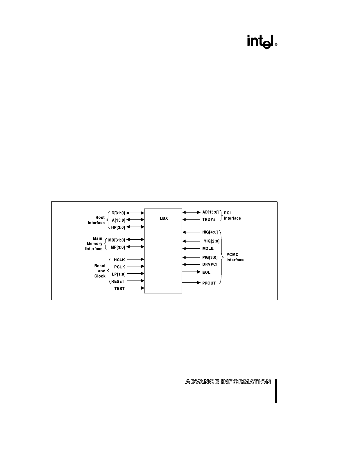
290478– 1
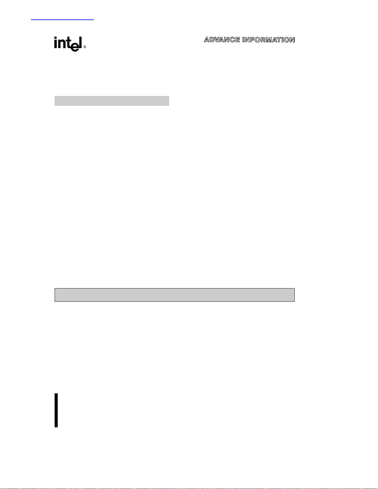
LBX Simplified Block Diagram
2
Page 3

82433LX/82433NX
LOCAL BUS ACCELERATOR (LBX)
CONTENTS PAGE
1.0 ARCHITECTURAL OVERVIEW
1.1 Buffers in the LBX АААААААААААААААААААААААААААААААААААААААААААААААААААААААААААААААААААААА 5
1.2 Control Interface Groups ААААААААААААААААААААААААААААААААААААААААААААААААААААААААААААААА 7
1.3 System Bus Interconnect ААААААААААААААААААААААААААААААААААААААААААААААААААААААААААААААА 7
1.4 PCI TRDYÝInterface ААААААААААААААААААААААААААААААААААААААААААААААААААААААААААААААААААА 8
1.5 Parity Support АААААААААААААААААААААААААААААААААААААААААААААААААААААААААААААААААААААААААА 8
2.0 SIGNAL DESCRIPTIONS ААААААААААААААААААААААААААААААААААААААААААААААААААААААААААААААААА 8
2.1 Host Interface Signals АААААААААААААААААААААААААААААААААААААААААААААААААААААААААААААААААА 9
2.2 Main Memory (DRAM) Interface Signals АААААААААААААААААААААААААААААААААААААААААААААААА 10
2.3 PCI Interface Signals АААААААААААААААААААААААААААААААААААААААААААААААААААААААААААААААААА 10
2.4 PCMC Interface Signals ААААААААААААААААААААААААААААААААААААААААААААААААААААААААААААААА 10
2.5 Reset and Clock Signals ААААААААААААААААААААААААААААААААААААААААААААААААААААААААААААААА 11
3.0 FUNCTIONAL DESCRIPTION ААААААААААААААААААААААААААААААААААААААААААААААААААААААААААА 12
3.1 LBX Post and Prefetch Buffers ААААААААААААААААААААААААААААААААААААААААААААААААААААААААА 12
3.1.1 CPU-TO-MEMORY POSTED WRITE BUFFER АААААААААААААААААААААААААААААААААААА 12
3.1.2 PCI-TO-MEMORY POSTED WRITE BUFFER ААААААААААААААААААААААААААААААААААААА 12
3.1.3 PCI-TO-MEMORY READ PREFETCH BUFFER ААААААААААААААААААААААААААААААААААА 12
3.1.4 CPU-TO-PCI POSTED WRITE BUFFER ААААААААААААААААААААААААААААААААААААААААААА 13
3.1.5 CPU-TO-PCI READ PREFETCH BUFFER ААААААААААААААААААААААААААААААААААААААААА 14
3.2 LBX Interface Command Descriptions ААААААААААААААААААААААААААААААААААААААААААААААААА 14
3.2.1 HOST INTERFACE GROUP: HIG[4:0
3.2.2 MEMORY INTERFACE GROUP: MIG[2:0
3.2.3 PCI INTERFACE GROUP: PIG[3:0
3.3 LBX Timing Diagrams АААААААААААААААААААААААААААААААААААААААААААААААААААААААААААААААААА 21
3.3.1 HIG[4:0]COMMAND TIMING ААААААААААААААААААААААААААААААААААААААААААААААААААААА 21
3.3.2 HIG[4:0]MEMORY READ TIMING АААААААААААААААААААААААААААААААААААААААААААААААА 22
3.3.3 MIG[2:0]COMMAND ААААААААААААААААААААААААААААААААААААААААААААААААААААААААААААА 23
3.3.4 PIG[3:0]COMMAND, DRVPCI, AND PPOUT TIMING ААААААААААААААААААААААААААААА 24
3.3.5 PIG[3:0]: READ PREFETCH BUFFER COMMAND TIMING АААААААААААААААААААААААА 25
3.3.6 PIG[3:0]: END-OF-LINE WARNING SIGNAL: EOL АААААААААААААААААААААААААААААААА 27
3.4 PLL Loop Filter Components АААААААААААААААААААААААААААААААААААААААААААААААААААААААААА 29
3.5 PCI Clock Considerations АААААААААААААААААААААААААААААААААААААААААААААААААААААААААААААА 30
ААААААААААААААААААААААААААААААААААААААААААААААААААААААААААА 5
]
АААААААААААААААААААААААААААААААААААААААААААА 14
]
АААААААААААААААААААААААААААААААААААААААА 18
]
ААААААААААААААААААААААААААААААААААААААААААААААА 19
3
Page 4

CONTENTS PAGE
4.0 ELECTRICAL CHARACTERISTICS
АААААААААААААААААААААААААААААААААААААААААААААААААААААА 31
4.1 Absolute Maximum Ratings АААААААААААААААААААААААААААААААААААААААААААААААААААААААААААА 31
4.2 Thermal Characteristics ААААААААААААААААААААААААААААААААААААААААААААААААААААААААААААААА 31
4.3 DC Characteristics АААААААААААААААААААААААААААААААААААААААААААААААААААААААААААААААААААА 32
4.3.1 82433LX LBX DC CHARACTERISTICS ААААААААААААААААААААААААААААААААААААААААААА 32
4.3.2 82433NX LBX DC CHARACTERISTICS ААААААААААААААААААААААААААААААААААААААААААА 33
4.4 82433LX AC Characteristics ААААААААААААААААААААААААААААААААААААААААААААААААААААААААААА 35
4.4.1 HOST AND PCI CLOCK TIMING, 66 MHz (82433LX) АААААААААААААААААААААААААААААА 35
4.4.2 COMMAND TIMING, 66 MHz (82433LX) АААААААААААААААААААААААААААААААААААААААААА 36
4.4.3 ADDRESS, DATA, TRDYÝ, EOL, TEST, TSCON AND PARITY TIMING, 66 MHz
(82433LX)
АААААААААААААААААААААААААААААААААААААААААААААААААААААААААААААААААААААААА 37
4.4.4 HOST AND PCI CLOCK TIMING, 60 MHz (82433LX) АААААААААААААААААААААААААААААА 38
4.4.5 COMMAND TIMING, 60 MHz (82433LX) АААААААААААААААААААААААААААААААААААААААААА 38
4.4.6 ADDRESS, DATA, TRDYÝ, EOL, TEST, TSCON AND PARITY TIMING, 60 MHz
(82433LX)
АААААААААААААААААААААААААААААААААААААААААААААААААААААААААААААААААААААААА 39
4.4.7 TEST TIMING (82433LX) ААААААААААААААААААААААААААААААААААААААААААААААААААААААААА 40
4.5 82433NX AC Characteristics ААААААААААААААААААААААААААААААААААААААААААААААААААААААААААА 40
4.5.1 HOST AND PCI CLOCK TIMING (82433NX) ААААААААААААААААААААААААААААААААААААААА 40
4.5.2 COMMAND TIMING (82433NX) ААААААААААААААААААААААААААААААААААААААААААААААААААА 41
4.5.3 ADDRESS, DATA, TRDYÝ, EOL, TEST, TSCON AND PARITY TIMING
(82433NX)
ААААААААААААААААААААААААААААААААААААААААААААААААААААААААААААААААААААААА 41
4.5.4 TEST TIMING (82433NX) ААААААААААААААААААААААААААААААААААААААААААААААААААААААААА 42
4.5.5 TIMING DIAGRAMS АААААААААААААААААААААААААААААААААААААААААААААААААААААААААААААА 43
5.0 PINOUT AND PACKAGE INFORMATION АААААААААААААААААААААААААААААААААААААААААААААААА 45
5.1 Pin Assignment АААААААААААААААААААААААААААААААААААААААААААААААААААААААААААААААААААААААА 45
5.2 Package Information АААААААААААААААААААААААААААААААААААААААААААААААААААААААААААААААААА 50
6.0 TESTABILITY ААААААААААААААААААААААААААААААААААААААААААААААААААААААААААААААААААААААААААА 51
6.1 NAND Tree ААААААААААААААААААААААААААААААААААААААААААААААААААААААААААААААААААААААААААА 51
6.1.1 TEST VECTOR TABLE ААААААААААААААААААААААААААААААААААААААААААААААААААААААААААА 51
6.1.2 NAND TREE TABLE АААААААААААААААААААААААААААААААААААААААААААААААААААААААААААААА 51
6.2 PLL Test Mode АААААААААААААААААААААААААААААААААААААААААААААААААААААААААААААААААААААААА 53
4
Page 5

82433LX/82433NX
1.0 ARCHITECTURAL OVERVIEW
The 82430 PCIset consists of the 82434LX PCMC
and 82433LX LBX components plus either a PCI/
ISA bridge or a PCI/EISA bridge. The 82430NX PCIset consists of the 82434NX PCMC and 82433NX
LBX components plus either a PCI/ISA bridge or a
PCI/EISA bridge. The PCMC and LBX provide the
core cache and main memory architecture and
serves as the Host/PCI bridge. An overview of the
PCMC follows the system overview section.
The Local Bus Accelerator (LBX) provides a high
performance data and address path for the
82430LX/82430NX PCIset. The LBX incorporates
five integrated buffers to increase the performance
of the Pentium processor and PCI master devices.
Two LBXs in the system support the following areas:
1. 64-bit data and 32-bit address bus of the Pentium
processor.
2. 32-bit multiplexed address/data bus of PCI.
3. 64-bit data bus of the main memory.
In addition, the LBXs provide parity support for the
three areas noted above (discussed further in Section 1.4).
1.1 Buffers in the LBX
The LBX components have five integrated buffers
designed to increase the performance of the Host
and PCI Interfaces of the 82430LX/82430NX
PCIset.
With the exception of the PCI-to-Memory write buffer
and the CPU-to-PCI write buffer, the buffers in the
LBX store data only, addresses are stored in the
PCMC component.
5
Page 6
82433LX/82433NX
290478– 2
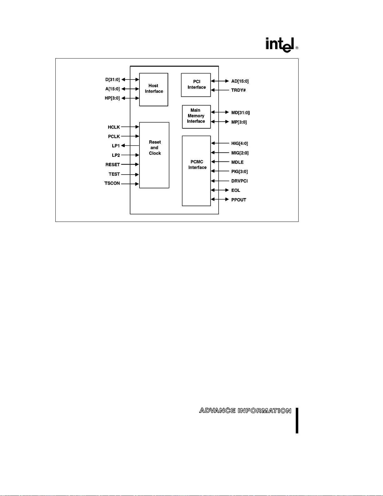
NOTES:
1. CPU-to-Memory Posted Write Buffer: This buffer is 4 Qwords deep, enabling the Pentium processor to write back a
whole cache line in 4-1-1-1 timing, a total of 7 CPU clocks.
2. PCI-to-Memory Posted Write Buffer: A PCI master can post two consecutive sets of 4 Dwords (total of one cache
line) or two single non-consecutive transactions.
3. PCI-to-Memory Read Prefetch Buffer: A PCI master to memory read transaction will cause this prefetch buffer to
read up to 4 Qwords of data from memory, allowing up to 8 Dwords to be read onto PCI in a single burst transaction.
4. CPU-to-PCI Posted Write Buffer: The Pentium processor can post up to 4 Dwords into this buffer. The TRDY
connect option allows zero-wait state burst writes to PCI, making this buffer especially useful for graphic write
operations.
5. CPU-to-PCI Read Prefetch Buffer: This prefetch buffer is 4 Dwords deep, enabling faster sequential Pentium processor reads when targeting PCI.
Figure 1. Simplified Block Diagram of the LBX Data Buffers
6
Ý
Page 7
82433LX/82433NX
1.2 Control Interface Groups
The LBX is controlled by the PCMC via the control
interface group signals. There are three interface
groups: Host, Memory, and PCI. These control
groups are signal lines that carry binary codes which
the LBX internally decodes in order to implement
specific functions such as latching data and steering
data from PCI to memory. The control interfaces are
described below.
1. Host Interface Group: These control signals are
named HIG[4:0]and define a total of 29 (30 for
the 82433NX) discrete commands. The PCMC
sends HIG commands to direct the LBX to perform functions related to buffering and storing
host data and/or address.
2. Memory Interface Group: These control signals
are named MIG[2:0]and define a total of 7 discrete commands. The PCMC sends MIG commands to direct the LBX to perform functions related to buffering, storing, and retiring data to
memory.
3. PCI Interface Group: These control signals are
named PIG[3:0]and define a total of 15 discrete
commands. The PCMC sends PIG commands to
direct the LBX to perform functions related to
buffering and storing PCI data and/or address.
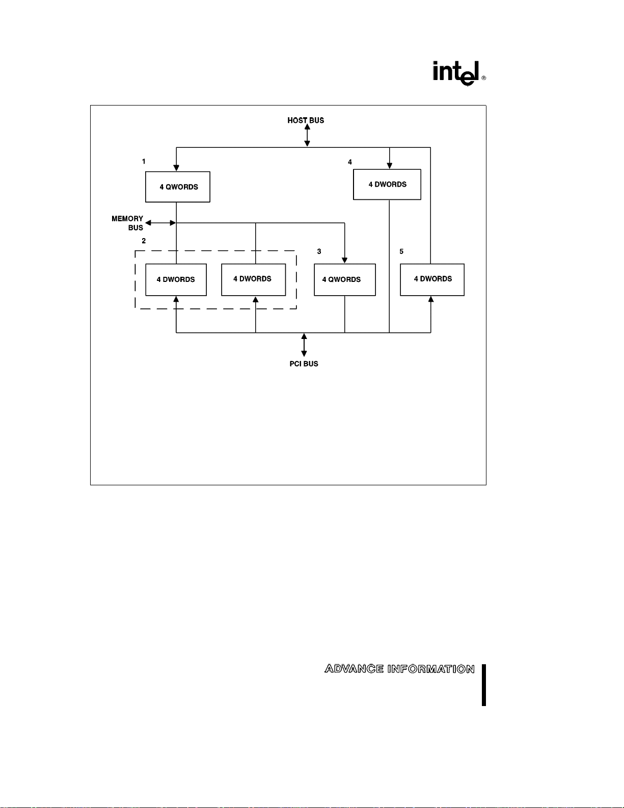
1.3 System Bus Interconnect
The architecture of the 82430/82430NX PCIset
splits the 64-bit memory and host data buses into
logical halves in order to manufacture LBX devices
with manageable pin counts. The two LBXs interface
to the 32-bit PCI AD[31:0]bus with 16 bits each.
Each LBX connects to 16 bits of the AD[31:0]bus
and 32-bits of both the MD[0:63]bus and the
D[0:63]bus. The lower order LBX (LBXL) connects
to the low word of the AD[31:0]bus, while the high
order LBX (LBXH) connects to the high word of the
AD[31:0]bus.
Since the PCI connection for each LBX falls on
16-bit boundaries, each LBX does not simply connect to either the low Dword or high Dword of the
Qword memory and host buses. Instead, the low order LBX buffers the first and third words of each
64-bit bus while the high order LBX buffers the second and fourth words of the memory and host
buses.
As shown in Figure 2, LBXL connects to the first and
third words of the 64-bit main memory and host data
buses. The same device also drives the first 16 bits
of the host address bus, A[15:0]. The LBXH device
connects to the second and fourth words of the
64-bit main memory and host data buses. Correspondingly, LBXH drives the remaining 16 bits of the
host address bus, A[31:16].
Figure 2. Simplified Interconnect Diagram of LBXs to System Buses
290478– 3
7
Page 8
82433LX/82433NX
1.4 PCI TRDYÝInterface
The PCI control signals do not interface to the LBXs,
instead these signals connect to the 82434LX
PCMC component. The main function of the LBXs
PCI interface is to drive address and data onto PCI
when the CPU targets PCI and to latch address and
data when a PCI master targets main memory.
The TRDY
Ý
option provides the capability for zerowait state performance on PCI when the Pentium
processor performs sequential writes to PCI. This
option requires that PCI TRDY
Ý
be connected to
each LBX, for a total of two additional connections in
the system. These two TRDY
addition to the single TRDY
Ý
connections are in
Ý
connection that the
PCMC requires.
1.5 Parity Support
The LBXs support byte parity on the host bus (CPU
and second level cache) and main memory buses
(local DRAM). The LBXs support parity during the
address and data phases of PCI transactions to/
from the host bridge.
2.0 SIGNAL DESCRIPTIONS
This section provides a detailed description of each
signal. The signals (Figure 3) are arranged in functional groups according to their associated interface.
Ý
The ‘
’ symbol at the end of a signal name indicates
that the active, or asserted state occurs when the
signal is at a low voltage level. When ‘
ent after the signal name, the signal is asserted
when at the high voltage level.
The terms assertion and negation are used extensively. This is done to avoid confusion when working
with a mixture of ‘active-low’ and ‘active-high’ signals. The term assert,orassertion indicates that a
signal is active, independent of whether that level is
represented by a high or low voltage. The term ne-
gate,ornegation indicates that a signal is inactive.
The following notations are used to describe the signal type.
in Input is a standard input-only signal.
out Totem Pole output is a standard active driver.
t/s Tri-State is a bi-directional, tri-state input/out-
put pin.
Ý
’ is not pres-
290478– 4
Figure 3. LBX Signals
8
Page 9
82433LX/82433NX
2.1 Host Interface Signals
Signal Type Description
A[15:0]t/s ADDRESS BUS: The bi-directional A[15:0]lines are connected to the address lines of the
D[31:0]t/s HOST DATA: The bi-directional D[31:0]lines are connected to the data lines of the host
HP[3:0]t/s HOST DATA PARITY: HP[3:0]are the bi-directional byte parity signals for the host data
host bus. The high order LBX (determined at reset time using the EOL signal) is
connected to A[31:16], and the low order LBX is connected to A[15:0]. The host address
bus is common with the Pentium processor, second level cache, PCMC and the two
LBXs. During CPU cycles A[31:3]are driven by the CPU and A[2:0]are driven by the
PCMC, all are inputs to the LBXs. During inquire cycles the LBX drives the PCI master
address onto the host address lines A[31:0]. This snoop address is driven to the CPU and
the PCMC by the LBXs to snoop L1 and the integrated second level tags, respectively.
During PCI configuration cycles bound for the PCMC, the LBXs will send or receive the
configuration data to/from the PCMC by copying the host data bus to/from the host
address bus. The LBX drives both halves of the Qword host data bus with data from the
32-bit address during PCMC configuration read cycles. The LBX drives the 32-bit address
with either the low Dword or the high Dword during PCMC configuration write cycles.
In the 82433NX, these pins contain weak internal pull-down resistors.
The high order 82433NX LBX samples A11 at the falling edge of reset to configure the
LBX for PLL test mode. When A11 is sampled low, the LBX is in normal operating mode.
When A11 is sampled high, the LBX drives the internal HCLK from the PLL on the EOL
pin. Note that A11 on the high order LBX is connected to the A27 line on the CPU address
bus. This same address line is used to put the PCMC into PLL test mode.
data bus. The high order LBX (determined at reset time using the EOL signal) is
connected to the host data bus D[63:48]and D[31:16]lines, and the low order LBX is
connected to the host data bus D[47:32]and D[15:0]lines. In the 82433LX, these pins
contain weak internal pull-up resistors.
In the 82433NX, these pins contain weak internal pull-down resistors.
bus. The low order parity bit HP[0]corresponds to D[7:0]while the high order parity bit
HP[3]corresponds to D[31:24]. The HP[3:0
cycles and as parity outputs during read cycles. Even parity is supported and the HP[3:0
signals follow the same timings as D[31:0
internal pull-up resistors.
In the 82433NX, these pins contain weak internal pull-down resistors.
]
signals function as parity inputs during write
]
. In the 82433LX, these pins contain weak
]
9
Page 10
82433LX/82433NX
2.2 Main Memory (Dram) Interface Signals
Signal Type Description
MD[31:0]t/s MEMORY DATA BUS: MD[31:0]are the bi-directional data lines for the memory data
MP[3:0]t/s MEMORY PARITY: MP[3:0]are the bi-directional byte enable parity signals for the
bus. The high order LBX (determined at reset time using the EOL signal) is connected to
the memory data bus MD[63:48]and MD[31:16]lines, and the low order LBX is
connected to the memory data bus MD[47:32]and MD[15:0]lines. The MD[31:0
signals drive data destined for either the host data bus or the PCI bus. The MD[31:0
signals input data that originated from either the host data bus or the PCI bus. These
pins contain weak internal pull-up resistors.
memory data bus. The low order parity bit MP[0]corresponds to MD[7:0]while the high
order parity bit MP[3]corresponds to MD[31:24]. The MP[3:0]signals are parity outputs
during write cycles to memory and parity inputs during read cycles from memory. Even
parity is supported and the MP[3:0]signals follow the same timings as MD[31:0]. These
pins contain weak internal pull-up resistors.
2.3 PCI Interface Signals
Signal Type Description
AD[15:0]t/s ADDRESS AND DATA: AD[15:0]are bi-directional data lines for the PCI bus. The
Ý
TRDY
AD[15:0]signals sample or drive the address and data on the PCI bus. The high order
LBX (determined at reset time using the EOL signal) is connected to the PCI bus
AD[31:16]lines, and the low order LBX is connected to the PCI AD[15:0]lines.
in TARGET READY: TRDYÝindicates the selected (targeted) device’s ability to complete
the current data phase of the bus operation. For normal operation, TRDYÝis tied
asserted low. When the TRDY
burst writes), TRDY
Ý
Ý
should be connected to the PCI bus.
option is enabled in the PCMC (for zero wait-state PCI
]
]
2.4 PCMC Interface Signals
Signal Type Description
HIG[4:0]in HOST INTERFACE GROUP: These signals are driven from the PCMC and control the
MIG[2:0]in MEMORY INTERFACE GROUP: These signals are driven from the PCMC and control
PIG[3:0]in PCI INTERFACE GROUP: These signals are driven from the PCMC and control the PCI
MDLE in MEMORY DATA LATCH ENABLE: During CPU reads from DRAM, the LBX uses a
DRVPCI in DRIVE PCI BUS: This signals enables the LBX to drive either address or data
10
host interface of the LBX. The 82433LX decodes the binary pattern of these lines to
perform 29 unique functions (30 for the 83433NX). These signals are synchronous to the
rising edge of HCLK.
the memory interface of the LBX. The LBX decodes the binary pattern of these lines to
perform 7 unique functions. These signals are synchronous to the rising edge of HCLK.
interface of the LBX. The LBX decodes the binary pattern of these lines to perform 15
unique functions. These signals are synchronous to the rising edge of HCLK.
clocked register to transfer data from the MD[31:0]and MP[3:0]lines to the D[31:0]and
HP[3:0]lines. MDLE is the clock enable for this register. Data is clocked into this register
when MDLE is asserted. The register retains its current value when MDLE is negated.
During CPU reads from main memory, the LBX tri-states the D[31:0]and HP[3:0]lines
on the rising edge of MDLE when HIG[4:0
information onto the PCI AD[15:0]lines.
e
]
NOPC.
Page 11
82433LX/82433NX
2.4 PCMC Interface Signals (Continued)
Signal Type Description
EOL t/s End Of Line: This signal is asserted when a PCI master read or write transaction is about
PPOUT t/s LBX PARITY: This signal reflects the parity of the 16 AD lines driven from or latched into
to overrun a cache line boundary. The low order LBX will have this pin connected to the
PCMC (internally pulled up in the PCMC). The high order LBX connects this pin to a pulldown resistor. With one LBX EOL line being pulled down and the other LBX EOL pulled
up, the LBX samples the value of this pin on the negation of the RESET signal to
determine if it’s the high or low order LBX.
the LBX, depending on the command driven on PIG[3:0]. The PCMC uses PPOUT from
both LBXs (called PPOUT[1:0]) to calculate the PCI parity signal (PAR) for CPU to PCI
transactions during the address phase of the PCI cycle. The LBX uses PPOUT to check
the PAR signal for PCI master transactions to memory during the address phase of the
PCI cycle. When transmitting data to PCI the PCMC uses PPOUT to calculate the proper
value for PAR. When receiving data from PCI the PCMC uses PPOUT to check the value
received on PAR.
If the L2 cache does not implement parity, the LBX will calculate parity so the PCMC can
drive the correct value on PAR during L2 reads initiated by a PCI master. The LBX
samples the PPOUT signal at the negation of reset and compares that state with the state
of EOL to determine whether the L2 cache implements parity. The PCMC internally pulls
down PPOUT[0]and internally pulls up PPOUT[1]. The L2 supports parity if PPOUT[0]is
connected to the high order LBX and PPOUT[1]is connected to the low order LBX. The
L2 is defined to not support parity if these connections are reversed, and for this case, the
LBX will calculate parity. For normal operations either connection allows proper parity to
be driven to the PCMC.
2.5 Reset and Clock Signals
Signal Type Description
HCLK in HOST CLOCK: HCLK is input to the LBX to synchronize command and data from the host
PCLK in PCI CLOCK: All timing on the LBX PCI interface is referenced to the PCLK input. All
RESET in RESET: Assertion of this signal resets the LBX. After RESET has been negated the LBX
LP1 out LOOP 1: Phase Lock Loop Filter pin. The filter components required for the LBX are
LP2 in LOOP 2: Phase Lock Loop Filter pin. The filter components required for the LBX are
TEST in TEST: The TEST pin must be tied low for normal system operation.
TSCON in TRI-STATE CONTROL: This signal enables the output buffers on the LBX. This pin must
and memory interfaces. This input is derived from a buffered copy of the PCMC HCLKx
output.
output signals on the PCI interface are driven from PCLK rising edges and all input signals
on the PCI interface are sampled on PCLK rising edges. This input is derived from a
buffered copy of the PCMC PCLK output.
configures itself by sampling the EOL and PPOUT pins. RESET is driven by the PCMC
CPURST pin. The RESET signal is synchronous to HCLK and must be driven directly by
the PCMC.
connected to these pins.
connected to these pins.
be held high for normal operation. If TSCON is negated, all LBX outputs will tri-state.
11
Page 12

82433LX/82433NX
3.0 FUNCTIONAL DESCRIPTION
3.1 LBX Post and Prefetch Buffers
This section describes the five write posting and
read prefetching buffers implemented in the LBX.
The discussion in this section refers to the operation
of both LBXs in the system.
3.1.1 CPU-TO-MEMORY POSTED WRITE
BUFFER
The write buffer is a queue 4 Qwords deep, it loads
Qwords from the CPU and stores Qwords to memory. It is 4 Qwords deep to accommodate write-backs
from the first or second level cache. It is organized
as a simple FIFO. Commands driven on the HIG[4:0
lines store Qwords into the buffer, while commands
on the MIG[2:0]lines retire Qwords from the buffer.
While retiring Qwords to memory, the DRAM controller unit of the PCMC will assert the appropriate MA,
]
CAS[7:0
track of full/empty states, status of the data and
address.
Byte parity for data to be written to memory is either
propagated from the host bus or generated by the
LBX. The LBX generates parity for data from the
second level cache when the second level cache
does not implement parity.
3.1.2 PCI-TO-MEMORY POSTED WRITE BUFFER
The buffer is organized as 2 buffers (4 Dwords
each). There is an address storage register for each
buffer. When an address is stored one of the two
buffers is allocated and subsequent Dwords of data
are stored beginning at the first location in that buffer. Buffers are retired to memory strictly in order,
Qword at a time.
Commands driven on the PIG[3:0]lines post addresses and data into the buffer. Commands driven
on HIG[4:0]result in addresses being driven on the
host address bus. Commands driven on MIG[2:0
result in data being retired to DRAM.
For cases where the address targeted by the first
Dword is odd, i.e. A[2
an even location in the buffer, the LBX correctly
aligns the Dword when retiring the data to DRAM. In
other words the buffer is capable of retiring a Qword
to memory where the data in the buffer is shifted by
Ý
, and WEÝsignals. The PCMC keeps
e
]
1, and the data is stored in
1 Dword (Dword is position 0 shifted to 1, 1 shifted
to 2 etc.). The DRAM controller of the PCMC asserts
the correct CAS[7:0
C/BE[3:0
Dword.
The End Of Line (EOL) signal is used to prevent PCI
master writes from bursting past the cache line
boundary. The device that provides ‘‘warning’’ to the
PCMC is the low order LBX. This device contains the
PCI master write low order address bits necessary to
determine how many Dwords are left to the end of
the line. Consequently, the LBX protocol uses the
EOL signal from the low order LBX to provide this
‘‘end-of-line’’ warning to the PCMC, so that it may
retry a PCI master write when it bursts past the
cache line boundary. This protocol is described fully
in Section 3.3.6.
]
The LBX calculates Dword parity on PCI write data,
sending the proper value to the PCMC on PPOUT.
The LBX generates byte parity on the MP signals for
writing into DRAM.
3.1.3 PCI-TO-MEMORY READ PREFETCH
This buffer is organized as a line buffer (4 Qwords)
for burst transfers to PCI. The data is transferred into
the buffer a Qword at a time and read out a Dword at
a time. The LBX then effectively decouples the
memory read rate from the PCI rate to increase concurrence.
Each new transaction begins by storing the first
Dword in the first location in the buffer. The starting
Dword for reading data out of the buffer onto PCI
must be specified within a Qword boundary; that is
the first requested Dword on PCI could be an even
or odd Dword. If the snoop for a PCI master read
results in a write-back from first or second level
caches, this write back is sent directly to PCI and
main memory. The following two paragraphs describe this process for cache line write-backs.
Since the write-back data from L1 is in linear order,
]
writing into the buffer is straightforward. Only those
Qwords to be transferred into PCI are latched into
the PCI-to-memory read buffer. For example, if the
address targeted by PCI is in the 3rd or 4th Qword in
the line, the first 2 Qwords of write back data are
discarded and not written into the read buffer. The
primary cache write-back must always be written
Ý
]
BUFFER
Ý
]
signals stored in the PCMC for that
signals depending on the PCI
12
Page 13

82433LX/82433NX
completely to the CPU-to-Memory posted Write
Buffer.
If the PCI master read data is read from the secondary cache, it is not written back to memory. Writebacks from the second level cache, when using
burst SRAMs, are in Pentium processor burst order
(the order depending on which Qword of the line is
targeted by the PCI read). The buffer is directly addressed when latching second level cache writeback data to accommodate this burst order. For example, if the requested Qword is Qword 1, then the
burst order is 1-0-3-2. Qword 1 is latched in buffer
location 0, Qword 0 is discarded, Qword 3 is latched
into buffer location 2 and Qword 2 is latched into
buffer location 1.
Commands driven on MIG[2:0]and HIG[4:0]enter
data into the buffer from the DRAM interface and the
host interface (i.e. the caches), respectively. Commands driven on the PIG[3:0]lines drive data from
the buffer onto the PCI AD[31:0]lines.
Parity driven on the PPOUT signal is calculated from
the byte parity received on the host bus or the memory bus, whichever is the source. If the second level
cache is the source of the data and does not implement parity, the parity driven on PPOUT is generated
by the LBX from the second level cache data. If
main memory is the source of the read data, PCI
parity is calculated from the DRAM byte parity. Main
memory must implement byte parity to guarantee
correct PCI parity generation.
3.1.4 CPU-TO-PCI POSTED WRITE BUFFER
The CPU-to-PCI Posted Write Buffer is 4 Dwords
deep. The buffer is constructed as a simple FIFO,
with some performance enhancements. An address
is stored in the LBX with each Dword of data. The
structure of the buffer accommodates the packetization of writes to be burst on PCI. This is accomplished by effectively discarding addresses of data
Dwords driven within a burst. Thus, while an address
is stored for each Dword, an address is not necessarily driven on PCI for each Dword. The PCMC determines when a burst write may be performed
based on consecutive addresses. The buffer also
enables consecutive bytes to be merged within a
single Dword, accommodating byte, word, and misaligned Dword string store and string move operations. Qword writes on the host bus are stored within
the buffer as two individual Dword writes, with separate addresses.
The storing of an address with each Dword of data
allows burst writes to be retried easily. In order to
retry transactions, the FIFO is effectively ‘‘backed
up’’ by one Dword. This is accomplished by making
the FIFO physically one entry larger than it is logically. Thus, the buffer is physically 5 entries deep (an
entry consists of an address and a Dword of data),
while logically it is considered full when 4 entries
have been posted. This design allows the FIFO to
be backed up one entry when it is logically full.
Commands driven on HIG[4:0]post addresses and
data into the buffer, and commands driven on
PIG[3:0]retire addresses and data from the buffer
and drive them onto the PCI AD[31:0]lines. As discussed previously, when bursting, not all addresses
are driven onto PCI.
Data parity driven on the PPOUT signal is calculated
from the byte parity received on the host bus. Address parity driven on PPOUT is calculated from the
address received on the host bus.
13
Page 14

82433LX/82433NX
3.1.5 CPU-TO-PCI READ PREFETCH BUFFER
This prefetch buffer is organized as a single buffer
4 Dwords deep. The buffer is organized as a simple
FIFO. reads from the buffer are sequential; the buffer does not support random access of its contents.
To support reads of less than a Dword the FIFO
read pointer can function with or without a pre-increment. The pointer can also be reset to the first entry
before a Dword is driven. When a Dword is read, it is
driven onto both halves of the host data bus.
Commands driven on the HIG[4:0]lines enable read
addresses to be sent onto PCI, the addresses are
driven using PIG[3:0]commands. Read data is
latched into the LBX by commands driven on the
PIG[3:0]lines and the data is driven onto the host
data bus using commands driven on the HIG[4:0
lines.
The LBX calculates Dword parity on PCI read data,
sending the proper value to the PCMC on PPOUT.
The LBX does not generate byte parity on the host
data bus when the CPU reads PCI.
3.2 LBX Interface Command
Descriptions
This section describes the functionality of the HIG,
MIG and PIG commands driven by the PCMC to the
LBXs.
3.2.1 HOST INTERFACE GROUP: HIG[4:0
The Host Interface commands are shown in Table 1.
These commands are issued by the host interface of
the PCMC to the LBXs in order to perform the following functions:
Reads from CPU-to-PCI read prefetch buffer
#
when the CPU reads from PCI.
Stores write-back data to PCI-to-memory read
#
]
prefetch buffer when PCI read address results in
a hit to a modified line in first or second level
caches.
Posts data to CPU-to-memory write buffer in the
#
case of a CPU to memory write.
Posts data to CPU-to-PCI write buffer in the case
#
of a CPU to PCI write.
Drives host address to Data lines and data to ad-
#
dress lines for programming the PCMC configuration registers.
]
14
Page 15
82433LX/82433NX
Table 1. HIG Commands
Command Code Description
NOPC 00000b No Operation on CPU Bus
CMR 11100b CPU Memory Read
CPRF 00100b CPU Read First Dword from CPU-to-PCI Read Prefetch Buffer
CPRA 00101b CPU Read Next Dword from CPU-to-PCI Read Prefetch Buffer, Toggle A
CPRB 00110b CPU Read Next Dword from CPU-to-PCI Read Prefetch Buffer, Toggle B
CPRQ 00111b CPU Read Qword from CPU-to-PCI Read Prefetch Buffer
SWB0 01000b Store Write-Back Data Qword 0 to PCI-to-Memory Read Buffer
SWB1 01001b Store Write-Back Data Qword 1 to PCI-to-Memory Read Buffer
SWB2 01010b Store Write-Back Data Qword 2 to PCI-to-Memory Read Buffer
SWB3 01011b Store Write-Back Data Qword 3 to PCI-to-Memory Read Buffer
PCMWQ 01100b Post to CPU-to-Memory Write Buffer Qword
PCMWFQ 01101b Post to CPU-to-Memory Write and PCI-to-Memory Read Buffer First Qword
PCMWNQ 01110b Post to CPU-to-Memory Write and PCI-to-Memory Read Buffer Next Qword
PCPWL 10000b Post to CPU-to-PCI Write Low Dword
MCP3L 10011b Merge to CPU-to-PCI Write Low Dword 3 Bytes
MCP2L 10010b Merge to CPU-to-PCI Write Low Dword 2 Bytes
MCP1L 10001b Merge to CPU-to-PCI Write Low Dword 1 Byte
PCPWH 10100b Post to CPU-to-PCI Write High Dword
MCP3H 10111b Merge to CPU-to-PCI Write High Dword 3 Bytes
MCP2H 10110b Merge to CPU-to-PCI Write High Dword 2 Bytes
MCP1H 10101b Merge to CPU-to-PCI Write High Dword 1 Byte
LCPRAD 00001b Latch CPU-to-PCI Read Address
DPRA 11000b Drive Address from PCI A/D Latch to CPU Address Bus
DPWA 11001b Drive Address from PCI-to-Memory Write Buffer to CPU Address Bus
ADCPY 11101b Address to Data Copy in the LBX
DACPYH 11011b Data to Address Copy in the LBX High Dword
DACPYL 11010b Data to Address Copy in the LBX Low Dword
PSCD 01111b Post Special Cycle Data
DRVFF 11110b Drive FF..FF (All 1’s) onto the Host Data Bus
PCPWHC 00011b Post to CPU-to-PCI Write High Dword Configuration
NOTE:
All other patterns are reserved.
15
Page 16
82433LX/82433NX
NOPC No Operation is performed on the host
bus by the LBX hence it tri-states its
host bus drivers.
CMR This command effectively drives
DRAM data onto the host data bus.
The LBX acts as a transparent latch in
this mode, depending on MDLE for
latch control. With the MDLE signal
high the CMR command will cause the
LBXs to buffer memory data onto the
host bus. When MDLE is low. The LBX
will drive onto the host bus whatever
memory data that was latched when
MDLE was negated.
CPRF This command reads the first Dword of
the CPU-to-PCI read prefetch buffer.
The read pointer of the FIFO is set to
point to the first Dword. The Dword is
driven onto the high and low halves of
the host data bus.
CPRA This command increments the read
pointer of the CPU-to-PCI read prefetch buffer FIFO and drives that
Dword onto the host bus when it is
driven after a CPRF or CPRB command. If driven after another CPRA
command, the LBX drives the current
Dword while the read pointer of the
FIFO is not incremented. The Dword is
driven onto the upper and lower halves
of the host data bus.
CPRB This command increments the read
pointer of the CPU-to-PCI read prefetch buffer FIFO and drives that
Dword onto the host bus when it is
driven after a CPRA command. If driven after another CPRB command, the
LBX drives the current Dword while the
read pointer of the FIFO is not incremented. The Dword is driven onto the
upper and lower halves of the host
data bus.
CPRQ This command drives the first Dword
stored in the CPU-to-PCI read prefetch
buffer onto the lower half of the host
data bus, and drives the second Dword
onto the upper half of the host data
bus, regardless of the state of the read
pointer. The read pointer is not affected by this command.
SWB0 This command stores a Qword from
the host data lines into location 0 of
the PCI-to-Memory Read Buffer. Parity
is either generated for the data or propagated from the host bus based on the
state of the PPOUT signals sampled at
the negation of RESET when the LBXs
were initialized.
SWB1 This command, (similar to SWB0),
stores a Qword from the host data
lines into location 1 of the PCI-to-Memory Read Buffer. Parity is either generated from the data or propagated from
the host bus based on the state of the
PPOUT signal sampled at the falling
edge of RESET.
SWB2 This command, (similar to SWB0),
stores a Qword written back from the
first or second level cache into location
2 of the PCI-to-memory read buffer.
Parity is either generated from the data
or propagated from the host bus based
on the state of the PPOUT signal sampled at the falling edge of RESET.
SWB3 This command stores a Qword from
the host data lines into location 3 of
the PCI-to-Memory Read Buffer. Parity
is either generated for the data or propagated from the host bus based on the
state of the PPOUT signal sampled at
the falling edge of RESET.
PCMWQ This command posts one Qword of
data from the host data lines to CPUto-Memory Write Buffer in case of a
CPU memory write or a write-back from
the second level cache.
PCMWFQ If the PCI Memory read address leads
to a hit on a modified line in the first
level cache, then a write-back is
scheduled and this data has to be written into the CPU-to-Memory Write Buffer and PCI-to-Memory Read Buffer at
the same time. The write-back of the
first Qword is done by this command to
both the buffers.
PCMWNQ This command follows the previous
command to store or post subsequent
write-back Qwords.
16
Page 17

82433LX/82433NX
PCPWL This command posts the low Dword of
a CPU-to-PCI write. The CPU-to-PCI
Write Buffer stores a Dword of PCI address for every Dword of data. Hence,
this command also stores the address
of the Low Dword in the address location for the data. Address bit 2 (A2) is
not stored directly. This command assumes a value of 0 for A2 and this is
what is stored.
MCP3L This command merges the 3 most sig-
nificant bytes of the low Dword of the
host data bus into the last Dword posted to the CPU-to-PCI write buffer. The
address is not modified.
MCP2L This command merges the 2 most sig-
nificant bytes of the low Dword of the
host data bus into the last Dword posted to the CPU-to-PCI write buffer. The
address is not modified.
MCP1L This command merges the most signif-
icant byte of the low Dword of the host
data bus into the last Dword posted to
the CPU-to-PCI write buffer. The address is not modified.
PCPWH This command posts the upper Dword
of a CPU-to-PCI write, with its address,
into the address location. Hence, to do
a Qword write PCPWL has to be followed by a PCPWH. Address bit 2 (A2)
is not stored directly. This command
forces a value of 1 for A2 and this is
what is stored.
MCP3H This command merges the 3 most sig-
nificant bytes of the high Dword of the
host data bus into the last Dword posted to the CPU-to-PCI Write Buffer. The
address is not modified.
MCP2H This command merges the 2 most sig-
nificant bytes of the high Dword of the
host data bus into the last Dword posted to the CPU-to-PCI Write Buffer. The
address is not modified.
MCP1H This command merges the most signif-
icant byte of the high Dword of the host
data bus into the last Dword posted to
the CPU-to-PCI Write Buffer. The address is not modified.
LCPRAD This command latches the host ad-
dress to drive on PCI for a CPU-to-PCI
read. It is necessary to latch the address in order to drive inquire addresses on the host address bus before the
CPU address is driven onto PCI.
DPRA The PCI memory read address is
latched in the PCI A/D latch by a PIG
command LCPRAD, this address is
driven onto the host address bus by
DPRA. Used in PCI to memory read
transaction.
DPWA The DPWA command drives the ad-
dress of the current PCI Master Write
Buffer onto the host address bus. This
command is potentially driven for multiple cycles. When it is no longer driven,
the read pointer will increment to point
to the next buffer, and a subsequent
DPWA command will read the address
from that buffer.
ADCPY This command drives the host data
bus with the host address. The address is copied on the high and low
halves of the Qword data bus; i.e.
A[31:0]is copied onto D[31:0]and
D[63:32]. This command is used when
the CPU writes to the PCMC configuration registers.
DACPYH This command drives the host address
bus with the high Dword of host data.
This command is used when the CPU
writes to the PCMC configuration registers.
DACPYL This command drives the host address
bus with the low Dword of host data.
This command is used when the CPU
writes to the PCMC configuration registers.
PSCD This command is used to post the val-
ue of the Special Cycle code into the
CPU-to-PCI Posted Write Buffer. The
value is driven onto the A[31:0]lines
by the PCMC, after acquiring the address bus by asserting AHOLD. The
value on the A[31:0]lines is posted
into the DATA location in the CPU-toPCI Posted Write Buffer.
DRVFF This command causes the LBX to drive
all ‘‘1s’’ (i.e. FFFFFFFFh) onto the host
data bus. It is used for CPU reads from
PCI that terminate with master abort.
PCPWHC This command posts the high half of
the CPU data bus. The LBXs post the
high half of the data bus even if A2
from the PCMC is low. This command
is used during configuration writes
when using PCI configuration access
mechanism
Ý
1.
17
Page 18

82433LX/82433NX
3.2.2 MEMORY INTERFACE GROUP: MIG[2:0
The Memory Interface commands are shown in Table 2. These commands are issued by the DRAM controller
of the PCMC to perform the following functions:
Retires data from CPU-to-Memory Write Buffer to DRAM.
#
Stores data into PCI-to-Memory Read Buffer when the PCI read address is targeted to DRAM.
#
Retires PCI-to-Memory Write Buffer to DRAM.
#
Command Code Description
NOPM 000b No Operation on Memory Bus
PMRFQ 001b Place into PCI-to-Memory Read Buffer First Qword
PMRNQ 010b Place into PCI-to-Memory Read Buffer Next Qword
RCMWQ 100b Retire CPU-to-Memory Write Buffer Qword
RPMWQ 101b Retire PCI-to-Memory Write Buffer Qword
RPMWQS 110b Retire PCI-to-Memory Write Buffer Qword Shifted
MEMDRV 111b Drive Latched Data Onto Memory Bus for 1 Clock Cycle
NOTE:
All other patterns are reserved.
NOPMN Operation on the memory bus. The LBX
PMRFQ The PCI-to-Memory read address tar-
PMRNQ This command stores subsequent
RCMWQ This command retires one Qword from
RPMWQ This command retires one Qword of
tri-states its drivers driving the memory
bus.
gets memory if there is a miss on first
and second caches. This command
stores the first Qword of data starting at
the first location in the buffer. This buffer is 8 Dwords or 1 cache line deep.
Qwords from memory starting at the
next available location in the PCI-toMemory Read Buffer. It is always used
after PMRFQ.
the CPU-to-Memory Write Buffer to
DRAM. The address is stored in the address queue for this buffer in the
PCMC.
data from one line of the PCI-to-Memory write buffer to DRAM. When all the
valid data in one buffer is retired, the
next RPMWQ (or RPMWQS) will read
data from the next buffer.
]
Table 2. MIG Commands
RPMWQS This command retires one Qword of
MEMDRV For a memory write operation the data
data from one line of PCI-to-Memory
write buffer to DRAM. For this command the data in the buffer is shifted by
one Dword (Dword in position 0 is shifted to 1, 1 to 2 etc.). This is because the
address targeted by the first Dword of
the write could be an odd Dword (i.e.,
address bit[2
ligned line this command has to be
used for all the data in the buffer. When
all the valid data in one buffer is retired,
the next RPMWQ (or RPMWQS) will
read data from the next buffer.
on the memory bus is required for more
than one clock cycle hence all DRAM
retires are latched and driven to the
memory bus in subsequent cycles by
this command.
]
is a 1). To retire a misa-
18
Page 19

82433LX/82433NX
3.2.3 PCI INTERFACE GROUP: PIG[3:0
The PCI Interface commands are shown in Table 3.
These commands are issued by the PCI master/
slave interface of the PCMC to perform the following
functions:
Slave posts address and data to PCI-to-Memory
#
Write Buffer.
Slave sends PCI-to-Memory read data on the AD
#
bus.
Slave latches PCI master memory address so
#
that it can be gated to the host address bus.
Master latches CPU-to-PCI read data from the
#
AD bus.
Master retires CPU-to-PCI write buffer.
#
Master sends CPU-to-PCI address to the AD bus.
#
Command Code PAR Description
PPMWA 1000b I Post to PCI-to-Memory Write Buffer Address
PPMWD 1001b I Post to PCI-to-Memory Write Buffer Data
SPMRH 1101b O Send PCI Master Read Data High Dword
SPMRL 1100b O Send PCI Master Read Data Low Dword
SPMRN 1110b O Send PCI Master Read Data Next Dword
LCPRF 0000b I Latch CPU Read from PCI into Read Prefetch Buffer First Dword
LCPRA 0001b I Latch CPU Read from PCI into Prefetch Buffer Next Dword, A Toggle
LCPRB 0010b I Latch CPU Read from PCI into Prefetch Buffer Next Dword, B Toggle
DCPWA 0100b O Drive CPU-to-PCI Write Buffer Address
DCPWD 0101b O Drive CPU-to-PCI Write Buffer Data
DCPWL 0110b O Drive CPU-to-PCI Write Buffer Last Data
DCCPD 1011b O Discard Current CPU-to-PCI Write Buffer Data
BCPWR 1010b O Backup CPU-to-PCI Write Buffer for Retry
SCPA 0111b O Send CPU-to-PCI Address
LPMA 0011b I Latch PCI Master Address
]
Table 3. PIG Commands
The PCI AD[31:0]lines are driven by asserting the
signal DRVPCI. This signal is used for both master
and slave transactions.
Parity is calculated on either the value being driven
onto PCI or the value being received on PCI, depending on the command. In Table 3, the PAR column has been included to indicate the value that the
PPOUT signals are based on. An ‘‘I’’ indicates that
the PPOUT signals reflect the parity of the AD lines
as inputs to the LBX. An ‘‘O’’ indicates that the
PPOUT signals reflect the value being driven on the
PCI AD lines. See Section 3.3.4 for the timing relationship between the PIG[3:0]command, the
AD[31:0]lines, and the PPOUT signals.
NOTE:
All other patterns are reserved.
19
Page 20

82433LX/82433NX
PPMWA This command selects a new buffer
and places the PCI master address
latch value into the address register
for that buffer. The next PPMWD
command posts write data in the first
location of this newly selected buffer. This command also causes the
EOL logic to decrement the count of
Dwords remaining in the line.
PPMWD This command stores the value in
the AD latch into the next data location in the currently selected buffer.
This command also causes the EOL
logic to decrement the count of
Dwords remaining in the line.
SPMRH This command sends the high order
Dword from the first Qword of the
PCI-to-Memory Read Buffer onto
PCI. This command also causes the
EOL logic to decrement the count of
Dwords remaining in the line.
SPMRL This command sends the low order
Dword from the first Qword of the
PCI-to-Memory Read Buffer onto
PCI. This command also selects the
Dword alignment for the transaction
and causes the EOL logic to decrement the count of Dwords remaining
in the line.
SPMRN This command sends the next
Dword from the PCI-to-Memory
Read Buffer onto PCI. This command also causes the EOL logic to
decrement the count of Dwords remaining in the line. This command is
used for the second and all subsequent Dwords of the current transaction.
LCPRF This command acquires the value of
the AD[31:0]lines into the first location in the CPU-to-PCI Read Prefetch Buffer until a different command is driven.
LCPRA When driven after a LCPRF or
LCPRB command, this command
latches the value of the AD[31:0
lines into the next location into the
CPU-to-PCI Read Prefetch Buffer.
When driven after another LCPRA
command, this command latches
the value on AD[31:0]into the same
location in the CPU-to-PCI Read
Prefetch Buffer, overwriting the previous value.
LCPRB When driven after a LCPRA com-
mand, this command latches the value of the AD[31:0]lines into the next
location into the CPU-to-PCI Read
Prefetch Buffer. When driven after
another LCPRB command, this command latches the value on AD[31:0
into the same location in the CPU-toPCI Read Prefetch Buffer, overwriting the previous value.
DCPWA This command drives the next ad-
dress in the CPU-to-PCI Write Buffer
onto PCI. The read pointer of the
FIFO is not incremented.
DCPWD This command drives the next data
Dword in the CPU-to-PCI Write Buffer onto PCI. The read pointer of the
FIFO is incremented on the next
PCLK if TRDY
Ý
is asserted.
DCPWL This command drives the previous
data Dword in the CPU-to-PCI Write
Buffer onto PCI. This is the data
which was driven by the last DCPWD
command. The read pointer of the
FIFO is not incremented.
DCCPD This command discards the current
Dword in the CPU-to-PCI Write Buffer. This is used to clear write data
when the write transaction terminates with master abort, where
Ý
TRDY
is never asserted.
BCPWR For this command the CPU-to-PCI
Write Buffer is ‘‘backed up’’ one entry such that the address/data pair
last driven with the DCPWA and
DCPWD commands will be driven
again on the AD[31:0]lines when
the commands are driven again.
This command is used when the target has retried the write cycle.
SCPA This command drives the value on
the host address bus onto PCI.
LPMA This command stores the previous
AD[31:0]value into the PCI master
]
address latch. If the EOL logic determines that the requested Dword is
the last Dword of a line, then the
EOL signal will be asserted; otherwise the EOL signal will be negated.
]
20
Page 21

82433LX/82433NX
3.3 LBX Timing Diagrams
This section describes the timing relationship between the LBX control signals and the interface
buses.
3.3.1 HIG[4:0]COMMAND TIMING
The commands driven on HIG[4:0]can cause the
host address bus and/or the host data bus to be
driven and latched. The following timing diagram illustrates the timing relationship between the driven
command and the buses. The ‘‘host bus’’ in Figure 4
could be address and/or data.
Note that the Drive command takes two cycles to
drive the host data bus, but only one to drive the
address. When the NOPC command is sampled, the
LBX takes only one cycle to release the host bus.
Figure 4. HIG[4:0]Command Timing
The Drive commands in Figure 4 are any of the
following:
CMR CPRF CPRA CPRB
CPRQ DPRA DPWA ADCPY
DACPYH DACPYL DRVFF
The Latch command in Figure 4 is any of the
following:
SWB0 SWB1 SWB2 SWB3
PCMWQ PCMWFQ PCMWNQ PCPWL
MCP3L MCP2L MCP1L PCPWH
MCP3H MCP2H LCPRAD PSCD
290478– 5
21
Page 22

82433LX/82433NX
3.3.2 HIG[4:0]MEMORY READ TIMING
Figure 5 illustrates the timing relationship between
Ý
]
the HIG[4:0], MIG[2:0], CAS[7:0
, and MDLE signals for DRAM memory reads. The delays shown in
the diagram do not represent the actual AC timings,
but are intended only to show how the delay affects
the sequencing of the signals.
When the CPU is reading from DRAM, the HIG[4:0
lines are driven with the CMR command that causes
the LBX to drive memory data onto the HD bus. Until
the MD bus is valid, the HD bus is driven with invalid
]
data. When CAS[7:0
comes valid after the DRAM CAS[7:0
Ý
assert, the MD bus be-
]
Ý
access
time. The MD and MP lines are directed through a
synchronous register inside the LBX to the HD and
HP lines. MDLE acts as a clock enable for this register. When MDLE is asserted, the LBX samples the
MD and MP lines. When MDLE is negated, the MD
and HD register retains its current value.
The LBX releases the HD bus based on sampling
the NOPC command on the HIG[4:0]lines and
MDLE being asserted. By delaying the release of the
]
HD bus until MDLE is asserted, the LBX provides
hold time for the data with respect to the write en-
]
Ý
able strobes (CWE[7:0
) of the second level
cache.
22
290478– 6
Figure 5. CPU Read from Memory
Page 23

82433LX/82433NX
3.3.3 MIG[2:0]COMMAND
Figure 6 illustrates the timing of the MIG[2:0]com-
Ý
]
mands with respect to the MD bus, CAS[7:0
Ý
WE
. Figure 6 shows the MD bus transitioning from
, and
a read to a write cycle.
The Latch command in Figure 6 is any of the
following:
PMRFQ PMRNQ
The Retire command in Figure 6 is any of the
following:
RCMWQ RPMWQ RPMWQS
Figure 6. MIG[2:0]Command Timing
The data on the MD bus is sampled at the end of the
first cycle into the LBX based on sampling the Latch
]
Ý
command. The CAS[7:0
in the next cycle. The WE
signals can be negated
Ý
signal is asserted in the
next cycle. The required delay between the assertion of WE
Ý
and the assertion of CAS[7:0
]
Ý
means
that the MD bus has 2 cycles to turn around; hence
the NOPM command driven in the second clock.
The LBX starts to drive the MD bus based on sampling the Retire command at the end of the third
clock. After the Retire command is driven for 1 cycle, the data is held at the output by the MEMDRV
command. The LBX releases the MD bus based on
sampling the NOPM command at the end of the
sixth clock.
290478– 7
23
Page 24

82433LX/82433NX
3.3.4 PIG[3:0]COMMAND, DRVPCI, AND PPOUT
TIMING
Figure 7 illustrates the timing of the PIG[3:0]commands, the DRVPCI signal, and the PPOUT[1:0]signal relative to the PCI AD[31:0]lines.
The Drive commands in Figure 7 are any of the following:
SPMRH SPMRL SPMRN
DCPWA DCPWD DCPWL
SCPA
The Latch commands in Figure 7 are any of the following:
PPMWA PPMWD LPMA
The following commands do not fit in either category, although they function like Latch type commands
with respect to the PPOUT[1:0]signals. They are
described in Section 3.3.5.
LCPRF LCPRA LCPRB
The DRVPCI signal is driven synchronous to the PCI
bus, enabling the LBXs to initiate driving the PCI
AD[31:0]lines one clock after DRVPCI is asserted.
As shown in Figure 7, if DRVPCI is asserted in cycle
N, the PCI AD[31:0]lines are driven in cycle N
a
The negation of the DRVPCI signal causes the LBXs
to asynchronously release the PCI bus, enabling the
LBXs to cease driving the PCI AD[31:0]lines in the
same clock that DRVPCI is negated. As shown in
Figure 7, if DRVPCI is negated in cycle N, the PCI
AD[31:0]lines are released in cycle N.
PCI address and data parity is available at the LBX
interface on the PPOUT lines from the LBX. The parity for data flow from PCI to LBX is valid 1 clock
cycle after data on the AD bus. The parity for data
flow from LBX to PCI is valid in the same cycle as
the data. When the AD[31:0]lines transition from
input to output, there is no conflict on the parity lines
due to the dead cycle for bus turnaround. This is
illustrated in the sixth and seventh clock of Figure 7.
1.
24
290478– 8
Figure 7. PIG[3:0]Command Timing
Page 25

82433LX/82433NX
3.3.5 PIG[3:0]: READ PREFETCH BUFFER
COMMAND TIMING
The structure of the CPU-to-PCI read prefetch buffer
requires special considerations due to the partition
of the PCMC and LBX. The PCMC interfaces only to
the PCI control signals, while the LBXs interface only
to the data. Therefore, it is not possible to latch a
Dword of data into the prefetch buffer after it is qualified by TRDY
latched into the same location until TRDY
pled asserted. Only after TRDY
Ý
. Instead, the data is repetitively
Ý
Ý
is sam-
is sampled asserted is data valid in the buffer. A toggling mechanism
is implemented to advance the write pointer to the
next Dword after the current Dword has been qualified by TRDY
Ý
.
Other considerations of the partition are taken into
account on the host side as well. When reading from
the buffer, the command to drive the data onto the
host bus is sent before it is known that the entry is
valid. This method avoids the wait-state that would
be introduced by waiting for an entry’s TRDY
Ý
to be
asserted before sending the command to drive the
entry onto the host bus. The FIFO structure of the
buffer also necessitates a toggling scheme to advance to the next buffer entry after the current entry
has been successfully driven. Also, this method
gives the LBX the ability to drive the same Dword
twice, enabling reads of less than a Dword to be
serviced by the buffer; reads of individual bytes of a
Dword would read the same Dword 4 times.
The HIG[4:0]and PIG[3:0]lines are defined to enable the features described previously. The LCPRF
PIG[3:0]command latches the first PCI read Dword
into the first location in the CPU-to-PCI read prefetch
Ý
buffer. This command is driven until TRDY
is sampled asserted. The valid Dword would then be in the
first location of the buffer. The cycle after TRDY
Ý
sampled asserted, the PCMC drives the LCPRA
command on the PIG[3:0]lines. This action latches
the value on the PCI AD[31:0]lines into the
next
Dword location in the buffer. Again, the LCPRA com-
Ý
mand is driven until TRDY
is sampled asserted.
Each cycle the LCPRA command is driven, data is
latched into the same location in the buffer. When
Ý
TRDY
is sampled asserted, the PCMC drives the
LCPRB command on the PIG[3:0]lines. This latches
the value on the AD[31:0]lines into the next location
in the buffer, the one
after
the location that the previ-
ous LCPRA command latched data into. After
Ý
TRDY
has been sampled asserted again, the command switches back to LCPRA. In this way, the
same location in the buffer can be filled repeatedly
until valid, and when it is known that the location is
valid, the next location can be filled.
The commands for the HIG[4:0], CPRF, CPRA, and
CPRB, work exactly the same way. If the same command is driven, the same data is driven. Driving an
appropriately different command results in the next
data being driven. Figure 8 illustrates the usage of
these commands.
is
25
Page 26

82433LX/82433NX
290478– 9
Figure 8. PIG[3:0]CPU-to-PCI Read Prefetch Buffer Commands
Figure 8 shows an example of how the PIG commands function on the PCI side. The LCPRF command is driven on the PIG[3:0]lines until TRDY
Ý
sampled asserted at the end of the fifth PCI clock.
The LCPRA command is then driven until TRDY
Ý
again sampled asserted at the end of the seventh
PCI clock. TRDY
Ý
is sampled asserted again so
LCPRB is driven only once. Finally, LCPRA is driven
again until the last TRDY
Ý
is asserted at the end of
the tenth PCI clock. In this way, 4 Dwords are
latched in the read CPU-to-PCI prefetch buffer.
Figure 8 also shows an example of how the HIG
commands function on the host side of the LBX.
Two clocks after sampling the CPRF command, the
LBX drives the host data bus. The data takes two
cycles to become stable. The first data driven in this
case is invalid, since the data has not arrived on PCI.
The data driven on the host bus changes in the seventh host clock, since the LCPRF command has
been driven on the PIG[3:0]lines the previous cycle,
latching a new value into the first location of the read
prefetch buffer. At this point the data is not the cor-
is
rect value, since TRDY
Ý
has not yet been asserted
on PCI. The LCPRF command is driven again in the
is
fifth PCI clock while TRDY
Ý
is sampled asserted at
the end of this clock. The requested data for the
read is then latched into the first location of the read
prefetch buffer and driven onto the host data bus,
becoming valid at the end of CPU clock 12. The
Ý
BRDY
signal can therefore be driven asserted in
this clock. The following read transaction (issued in
CPU clock 15) requests the next Dword, and so the
CPRA command is driven on the HIG[4:0]lines, advancing to read the next location in the read prefetch buffer. As the correct data is already there, the
command is driven only once for this transaction.
The next read transaction requests data in the same
Dword as the previous. Therefore, the CPRA command is driven again, the buffer is not advanced,
and the same Dword is driven onto the host bus.
26
Page 27

82433LX/82433NX
3.3.6 PIG[3:0]: END-OF-LINE
WARNING SIGNALS: EOL
When posting PCI master writes, the PCMC must be
informed when the line boundary is about to be overrun, as it has no way of determining this itself (recall
that the PCMC does not receive any address bits
from PCI). The low order LBX determines this, as it
contains the low order bits of the PCI master write
address and also tracks how many Dwords of write
data have been posted. Therefore, the low order
LBX component sends the ‘‘end-of-line’’ warning to
the PCMC. This is accomplished with the EOL signal
driven from the low order LBX to the PCMC. Figure 9
illustrates the timing of this signal.
1. The FRAME
Ý
signal is sampled asserted in the
first cycle. The LPMA command is driven on the
PIG[3:0]signals to hold the address while it is
being decoded (e.g. in the MEMCS
Ý
decode circuit of the 82378 SIO). The first data (D0) remains
on the bus until TRDY
Ý
to MEMCS
being sampled asserted in the third
Ý
is asserted in response
clock.
2. The PPMWA command is driven in response to
sampling MEMCS
Ý
asserted. TRDYÝis asserted
in this cycle indicating that D0 has been latched at
the end of the fourth clock. The action of the
PPMWA command is to transfer the PCI address
captured in the PCI AD latch at the end of the first
clock to the posting buffer, and open the PCI AD
latch in order to capture the data. This data will be
posted to the write buffer in the following cycle by
the PPMWD command.
3. The EOL signal is first negated when the LPMA
command is driven on the PIG[3:0]signals. However, if the first data Dword accepted is also the
last that should be accepted, the EOL signal will
be asserted in the third clock. This is the ‘‘end-ofline’’ indication. In this case, the EOL signal is asserted as soon as the LPMA command has been
latched. The action by the PCMC in response is to
Ý
negate TRDY
and assert STOPÝin the fifth
clock. Note that the EOL signal is asserted even
before the MEMCS
Ý
signal is sampled asserted
in this case. The EOL signal will remain asserted
until the next time the LPMA command is driven.
4. If the second Dword is the last that should be
accepted, the EOL signal will be asserted in the
fifth clock to negate TRDYÝand assert STOP
on the following clock. The EOL signal is asserted
in response to the PPMWA command being sampled, and relies on the knowledge that TRDY
Ý
for
the first Dword of data will be sampled asserted
by the master in the same cycle (at the end of the
fourth clock). Therefore, to prevent a third assertion of TRDYÝin the sixth clock, the EOL signal
must be asserted in the fifth clock.
Ý
Figure 9. EOL Signal Timing for PCI Master Writes
290478– 10
27
Page 28

82433LX/82433NX
A similar sequence is defined for PCI master reads.
While it is possible to know when to stop driving read
data due to the fact that the read address is latched
into the PCMC before any read data is driven on PCI,
the use of the EOL signal for PCI master reads simplifies the logic internal to the PCMC. Figure 10 illustrates the timing of EOL with respect to the PIG[3:0
commands to drive out PCI read data.
Note that unlike the PCI master write sequence, the
Ý
STOP
signal is asserted with the last data transfer,
not after.
1. The LPMA command sampled at the end of the
second clock causes the EOL signal to assert if
there is only one Dword left in the line, otherwise
it will be negated. The first TRDY
the last, and the STOP
Ý
]
with TRDY
2. The SPMRH command causes the count of the
.
Ý
signal will be asserted
Ý
number of Dwords left in the line to be decremented. If this count reaches one, the EOL signal
is asserted. The next TRDY
Ý
STOP
is asserted with TRDYÝ.
Ý
will be the last, and
will also be
28
290478– 11
Figure 10. EOL Signal Timing for PCI Master Reads
Page 29

82433LX/82433NX
3.4 PLL Loop Filter Components
As shown in Figure 11, loop filter components are
required on the LBX components. A 4.7 KX 5% resistor is typically connected between pins LP1 and
LP2. Pin LP2 has a path to the PLLAGND pin
through a 100X 5% series resistor and a 0.01 mF
10% series capacitor. The ground side of capacitor
C1 and the PLLVSS pin should connect to the
ground plane at a common point. All PLL loop filter
traces should be kept to minimal length and should
be wider than signal traces. Inductor L1 is connected to the 5V power supply on both the 82433LX and
82433NX.
Some circuit boards may require filtering the power
circuit to the LBX PLL. The circuit shown in Figure
11 will typically enable the LBX PLL to have higher
noise immunity than without. Pin PLLVDD is connected to the 5V V
The PLLVDD and PLLVSS pins are bypassed with a
0.01 mF 10% series capacitor.
through a 10X 5% resistor.
CC
The high order 82433NX LBX samples A11 at the
falling edge of reset to configure the LBX for PLL
test mode. When A11 is sampled low, the LBX is in
normal operating mode. When A11 is sampled high,
the LBX drives the internal HCLK from the PLL on
the EOL pin. Note that A11 on the high order LBX is
connected to the A27 line on the CPU address bus.
This same address line is used to put the PCMC into
PLL test mode.
Mercury Mercury
60 MHz 66 MHz
Neptune
R1 4.7 KX 2.2 KX 4.7 KX
R2 100X 100X 100X
C2 0.01 mF 0.01 mF 0.01 mF
R3 10X 10X 10X
C1 0.47 mF 0.47 mF 0.47 mF
1
C1
0.01 mF 0.01 mF 0.01 mF
Figure 11. Loop Filter Circuit
290478– 12
29
Page 30

82433LX/82433NX
3.5 PCI Clock Considerations
There is a 1.25 ns clock skew specification between
the PCMC and the LBX that must be adhered to for
proper operation of the PCMC/LBX timing. As
shown in Figure 12, the PCMC drives PCLKOUT to
an external clock driver which supplies copies of
PCLK to PCI devices, the LBXs, and back to the
PCMC. The skew specification is defined as the dif-
Figure 12. Clock Considerations
ference in timing between the signal that appears at
the PCMC PCLKIN input pin and the signal that appears at the LBX PCLK input pin. For both the low
order LBX and the high order LBX, the PCLK rising
and falling edges must not be more than 1.25 ns
apart from the rising and falling edge of the PCMC
PCLKIN signal.
290478– 13
30
Page 31

82433LX/82433NX
4.0 ELECTRICAL CHARACTERISTICS
Maximum Power Dissipation: АААААА1.4W (82433LX)
Maximum Total Power Dissipation À1.4W (82433NX)
4.1 Absolute Maximum Ratings
Table 4 lists stress ratings only. Functional operation
at these maximums is not guaranteed. Functional
operation conditions are given in Sections 4.2
and 4.3.
Extended exposure to the Absolute Maximum Ratings may affect device reliability.
Case Temperature under Bias ААААААА0
Storage Temperature ААААААААААb40§Ctoa125§C
Voltage on Any Pin
with Respect to GroundААААА
b
Supply Voltage
with Respect to V
ААААААААААААb0.3 toa7.0V
SS
0.3 to V
Ctoa85§C
§
a
0.3V
CC
Maximum Power Dissipation, V
The maximum total power dissipation in the
82433NX on the V
pins may draw as much as 430 mW, however,
V
CC3
total power will not exceed 1.4W.
NOTICE: This data sheet contains information on
products in the sampling and initial production phases
of development. The specifications are subject to
change without notice. Verify with your local Intel
Sales office that you have the latest data sheet before finalizing a design.
*
WARNING: Stressing the device beyond the ‘‘Absolute
Maximum Ratings’’ may cause permanent damage.
These are stress ratings only. Operation beyond the
‘‘Operating Conditions’’ is not recommended and extended exposure beyond the ‘‘Operating Conditions’’
may affect device reliability.
CC
and V
АААААААА430 mW
CC3
pins is 1.4W. The
CC3
4.2 Thermal Characteristics
The LBX is designed for operation at case temperatures between 0§C and 85§C. The thermal resistances of
the package are given in the following tables.
Parameter Air Flow Rate (Linear Feet per Minute)
iJA(§C/Watt) 51.9 37.1 34.8
iJC(§C/Watt) 10
Table 4. Thermal Resistance
0 400 600
31
Page 32

82433LX/82433NX
4.3 DC Characteristics
Host Interface Signals
A[15:0](t/s), D[31:0](t/s), HIG[4:0](in), HP[3:0](t/s)
Main Memory (DRAM) Interface Signals
MD[31:0](t/s), MP[3:0](t/s), MIG[2:0](in), MDLE(in)
PCI Interface Signals
AD[15:0](t/s), TRDY
Ý
(in), PIG[3:0](in), DRVPCI(in),
EOL(t/s), PPOUT(t/s)
Reset and Clock Signals
HCLK(in), PCLK(in), RESET(in), LP1(out), LP2(in),
TEST(in)
4.3.1 82433LX LBX DC CHARACTERISTICS
Functional Operating Range: V
e
4.75 V to 5.25V; T
CC
CASE
e
0§Ctoa85§C
Symbol Parameter Min Typical Max Unit Notes
V
IL1
V
IH1
V
IL2
V
IH2
V
OL1
V
OH1
V
OL2
V
OH2
I
OL1
I
OH1
I
OL2
I
OH2
Input Low Voltage
Input High Voltage 2.0 V
Input Low Voltage
Input High Voltage 0.7cV
Output Low Voltage 0.4 V 3
Output High Voltage 2.4 V 3
Output Low Voltage 0.5 V 4
Output High Voltage V
Output Low Current 1 mA 5
Output High Current
Output Low Current 3 mA 6
Output High Current
b
0.3 0.8 V 1
a
0.3 V 1
CC
b
0.3 0.3cV
CC
b
0.5 V 4
CC
b
1mA5
b
2mA6
CC
a
V
0.3 V 2
CC
V2
32
Page 33

82433LX/82433NX
Functional Operating Range: V
e
4.75V to 5.25V; T
CC
CASE
e
0§Ctoa85§C (Continued)
Symbol Parameter Min Typical Max Unit Notes
I
OL3
I
OH3
I
IH
I
IL
C
IN
C
OUT
C
I/O
NOTES:
and V
1. V
IL1
HCLK, PCLK
and V
2. V
IL2
and V
3. V
OL1
and V
4. V
OL2
and I
5. I
OL1
and I
6. I
OL2
and I
7. I
OL3
Output Low Current 3 mA 7
Output High Current
Input Leakage Current
Input Leakage Current
b
1mA7
a
10 mA
b
10 mA
Input Capacitance 4.6 pF
Output Capacitance 4.3 pF
I/O Capacitance 4.6 pF
apply to the following signals: AD[15:0],A[15:0],D[31:0],HP[3:0],MD[31:0],MP[3:0], TRDYÝ, RESET,
IH1
apply to the following signals: HIG[4:0], PIG[3:0], MIG[2:0], MDLE, DRVPCI
IH2
apply to the following signals: AD[15:0],A[15:0],D[31:0],HP[3:0],MD[31:0],MP[3:0
OH1
apply to the following signals: PPOUT, EOL
OH2
apply to the following signals: PPOUT, EOL
OH1
apply to the following signals: AD[15:0
OH2
apply to the following signals: A[15:0],D[31:0],HP[3:0],MD[31:0],MP[3:0
OH3
]
]
]
4.3.2 82433NX LBX DC CHARACTERISTICS
Functional Operating Range: V
e
4.75V to 5.25V; V
CC
e
3.135 to 3.465V, T
CC3
CASE
e
0§Ctoa85§C
Symbol Parameter Min Typical Max Unit Notes
V
IL1
V
IH1
V
IL2
V
IH2
V
IL3
V
IH3
V
OL1
V
OH1
V
OL2
V
OH2
I
OL1
I
OH1
I
OL2
I
OH2
Input Low Voltage
Input High Voltage 2.0 V
Input Low Voltage
Input High Voltage 0.7 x V
Input Low Voltage
Input High Voltage 2.0 V
Output Low Voltage 0.4 V 4
Output High Voltage 2.4 V 4
Output Low Voltage 0.5 V 5
Output High Voltage V
Output Low Current 1 mA 6
Output High Current
Output Low Current 3 mA 7
Output High Current
b
0.3 0.8 V 1
a
0.3 V 1
CC
b
0.3 0.3 x V
CC
b
0.3 0.8 V 3
b
0.5 V 5
CC
b
1mA6
b
2mA7
CC
a
V
0.3 V 2
CC
a
0.3 V 3
CC3
V2
33
Page 34

82433LX/82433NX
Functional Operating Range: V
e
T
CASE
e
4.75V to 5.25V; V
CC
0§Ctoa85§C (Continued)
e
3.135V to 3.465V,
CC3
Symbol Parameter Min Typical Max Unit Notes
I
OL3
I
OH3
I
IH
I
IL
C
IN
C
OUT
C
I/O
NOTES:
and V
1. V
IL1
and V
2. V
IL2
and V
3. V
IL3
and V
4. V
OL1
and V
5. V
OL2
and I
6. I
OL1
and I
7. I
OL2
and I
8. I
OL3
9. The output buffers for A[15:0],D[31:0]and HP[3:0]are powered with V
Output Low Current 3 mA 8
Output High Current
Input Leakage Current
Input Leakage Current
b
1mA8
a
10 mA
b
10 mA
Input Capacitance 4.6 pF
Output Capacitance 4.3 pF
I/O Capacitance 4.6 pF
apply to the following signals: AD[15:0],MD[31:0],MP[3:0], TRDYÝ, RESET, HCLK, PCLK
IH1
apply to the following signals: HIG[4:0], PIG[3:0], MIG[2:0], MDLE, DRVPCI
IH2
apply to the following signals: A[15:0],D[31:0],HP[3:0
IH3
apply to the following signals: AD[15:0],A[15:0],D[31:0],HP[3:0],MD[31:0],MP[3:0
OH1
apply to the following signals: PPOUT, EOL
OH2
apply to the following signals: PPOUT, EOL
OH1
apply to the following signals: AD[15:0
OH2
apply to the following signals: A[15:0],D[31:0],HP[3:0],MD[31:0],MP[3:0
OH3
]
]
and therefore drive 3.3V signal levels.
CC3
]
]
34
Page 35

82433LX/82433NX
e
4.4 82433LX AC Characteristics
The AC specifications given in this section consist of
propagation delays, valid delays, input setup requirements, input hold requirements, output float delays,
output enable delays, clock high and low times and
clock period specifications. Figure 13 through Figure
In Figure 13 through Figure 21 VT
lowing signals: MD[31:0],MP[3:0],D[31:0],
HP[3:0],A[15:0],AD[15:0], TRDY
RESET, TEST.
e
VT
2.5V for the following signals: HIG[4:0],
PIG[3:0], MIG[2:0], MDLE, DRVPCI, PPOUT, EOL.
21 define these specifications. Sections 4.3.1
through 4.3.3 list the AC Specifications.
4.4.1 HOST AND PCI CLOCK TIMING, 66 MHZ (82433LX)
Functional Operating Range: V
e
4.9V to 5.25V; T
CC
CASE
e
0§Ctoa70§C
Symbol Parameter Min Max Figure Notes
t1a HCLK Period 15 20 18
t1b HCLK High Time 5 18
t1c HCLK Low Time 5 18
t1d HCLK Rise Time 1.5 19
t1e HCLK Fall Time 1.5 19
t1f HCLK Period Stability
g
100 ps
t2a PCLK Period 30 18
t2b PCLK High Time 12 18
t2c PCLK Low Time 12 18
t2d PCLK Rise Time 3 19
t2e PCLK Fall Time 3 19
t3 HCLK to PCLK Skew
b
7.2 5.8 21
1.5V for the fol-
Ý
, HCLK, PCLK,
1
NOTE:
1. Measured on rising edge of adjacent clocks at 1.5 Volts.
35
Page 36

82433LX/82433NX
4.4.2 COMMAND TIMING, 66 MHZ (82433LX)
Functional Operating Range: V
e
4.9V to 5.25V; T
CC
Symbol Parameter Min Max Figure Notes
t10a HIG[4:0]Setup Time to HCLK Rising 5.4 15
t10b HIG[4:0]Hold Time from HCLK Rising 0 15
t11a MIG[2:0]Setup Time to HCLK Rising 5.4 15
t11b MIG[2:0]Hold Time from HCLK Rising 0 15
t12a PIG[3:0]Setup Time to PCLK Rising 15.6 15
t12b PIG[3:0]Hold Time from PCLK Rising
b
1.0 15
t13a MDLE Setup Time to HCLK Rising 5.7 15
t13b MDLE Hold Time to HCLK Rising
b
0.3 15
t14a DRVPCI Setup Time to PCLK Rising 6.5 15
t14b DRVPCI Hold Time from PCLK Rising
b
0.5 15
t15a RESET Setup Time to HCLK Rising 3.1 15
t15b RESET Hold Time from HCLK Rising 0.3 15
CASE
e
0§Ctoa70§C
36
Page 37

82433LX/82433NX
4.4.3 ADDRESS, DATA, TRDYÝ, EOL, TEST, TSCON AND PARITY TIMING, 66 MHz (82433LX)
Functional Operating Range: V
e
4.9V to 5.25V; T
CC
Symbol Parameter Min Max Figure Notes
t20a AD[15:0]Output Enable Delay from PCLK Rising 2 17
t20b AD[15:0]Valid Delay from PCLK Rising 2 11 14 1
t20c AD[15:0]Setup Time to PCLK Rising 7 15
t20d AD[15:0]Hold Time from PCLK Rising 0 15
t20e AD[15:0]Float Delay from DRVPCI Falling 2 10 16
t21a TRDYÝSetup Time to PCLK Rising 7 15
t21b TRDYÝHold Time from PCLK Rising 0 15
t22a D[31:0],HP[3:0]Output Enable Delay from HCLK Rising 0 7.7 17 2
t22b D[31:0],HP[3:0]Float Delay from HCLK Rising 3.1 15.5 16
t22c D[31:0],HP[3:0]Float Delay from MDLE Rising 2 11.0 16 3
t22d D[31:0],HP[3:0]Valid Delay from HCLK Rising 0 7.7 14 2
t22e D[31:0],HP[3:0]Setup Time to HCLK Rising 3.0 15
t22f D[31:0],HP[3:0]Hold Time from HCLK Rising 0.3 15
t23a HA[15:0]Output Enable Delay from HCLK Rising 0 15.2 17
t23b HA[15:0]Float Delay from HCLK Rising 0 15.2 16
t23c HA[15:0]Valid Delay from HCLK Rising 0 16 14 7
t23cc HA[15:0]Valid Delay from HCLK Rising 0 14.5 8
t23d HA[15:0]Setup Time to HCLK Rising 15 15 4
t23e HA[15:0]Setup Time to HCLK Rising 4.1 15 5
]
t23f HA[15:0
Hold Time from HCLK Rising 0.3 15
t24a MD[31:0],MP[3:0]Valid Delay from HCLK Rising 0 12.0 14 6
t24b MD[31:0],MP[3:0]Setup Time to HCLK Rising 4.0 15
t24c MD[31:0],MP[3:0]Hold Time from HCLK Rising 0.4 15
t25 EOL, PPOUT Valid Delay from PCLK Rising 2.3 17.2 14 2
t26a All Outputs Float Delay from TSCON Falling 0 30 16
t26b All Outputs Enable Delay from TSCON Rising 0 30 17
CASE
e
0§Ctoa70§C
NOTES:
1. Min: 0 pF, Max: 50 pF
2.0pF
3. When NOPC command sampled on previous rising HCLK on HIG[4:0
4. CPU to PCI Transfers
5. When ADCPY command is sampled on HIG[4:0
6. 50 pF
7. When DACPYL or DACPYH commands are sampled on HIG[4:0
8. Inquire cycle
]
]
]
37
Page 38

82433LX/82433NX
4.4.4 HOST AND PCI CLOCK TIMING, 60 MHz (82433LX)
Functional Operating Range: V
e
4.75V to 5.25V; T
CC
Symbol Parameter Min Max Figure Notes
t1a HCLK Period 16.6 20 18
t1b HCLK High Time 5.5 18
t1c HCLK Low Time 5.5 18
t1d HCLK Rise Time 1.5 19
t1e HCLK Fall Time 1.5 19
t1f HCLK Period Stability
t2a PCLK Period 33.33 18
t2b PCLK High Time 13 18
t2c PCLK Low Time 13 18
t2d PCLK Rise Time 3 19
t2e PCLK Fall Time 3 19
t3 PCLK to PCMC PCLKIN: Input to Input Skew
NOTES:
1. Measured on rising edge of adjacent clocks at 1.5 Volts
b
7.2 5.8 21
4.4.5 COMMAND TIMING, 60 MHZ (82433LX)
e
Functional Operating Range: V
4.75V to 5.25V; T
CC
Symbol Parameter Min Max Figure Notes
t10a HIG[4:0]Setup Time to HCLK Rising 6.0 15
]
t10b HIG[4:0
Hold Time from HCLK Rising 0 15
t11a MIG[2:0]Setup Time to HCLK Rising 6.0 15
t11b MIG[2:0]Hold Time from HCLK Rising 0 15
t12a PIG[3:0]Setup Time to PCLK Rising 16.0 15
t12b PIG[3:0]Hold Time from PCLK Rising 0 15
t13a MDLE Setup Time to HCLK Rising 5.9 15
t13b MDLE Hold Time to HCLK Rising
b
0.3 15
t14a DRVPCI Setup Time to PCLK Rising 7.0 15
t14b DRVPCI Hold Time from PCLK Rising
b
0.5 15
t15a RESET Setup Time to HCLK Rising 3.4 15
t15b RESET Hold Time from HCLK Rising 0.4 15
e
CASE
CASE
0§Ctoa85§C
g
100 ps
e
0§Ctoa85§C
1
38
Page 39

82433LX/82433NX
4.4.6 ADDRESS, DATA, TRDYÝ, EOL, TEST, TSCON AND PARITY TIMING, 60 MHz (82433LX)
Functional Operating Range: V
e
4.75V to 5.25V; T
CC
Symbol Parameter Min Max Figure Notes
t20a AD[15:0]Output Enable Delay from PCLK Rising 2 17
t20b AD[15:0]Valid Delay from PCLK Rising 2 11 14 1
t20c AD[15:0]Setup Time to PCLK Rising 7 15
t20d AD[15:0]Hold Time from PCLK Rising 0 15
t20e AD[15:0]Float Delay from DRVPCI Falling 2 10 16
t21a TRDYÝSetup Time to PCLK Rising 7 15
t21b TRDYÝHold Time from PCLK Rising 0 15
t22a D[31:0],HP[3:0]Output Enable Delay from HCLK Rising 0 7.9 17 2
t22b D[31:0],HP[3:0]Float Delay from HCLK Rising 3.1 15.5 16
t22c D[31:0],HP[3:0]Float Delay from MDLE Rising 2 11.0 16 3
t22d D[31:0],HP[3:0]Valid Delay from HCLK Rising 0 7.8 14 2
t22e D[31:0],HP[3:0]Setup Time to HCLK Rising 3.4 15
t22f D[31:0],HP[3:0]Hold Time from HCLK Rising 0.3 15
t23a HA[15:0]Output Enable Delay from HCLK Rising 0 15.2 17
t23b HA[15:0]Float Delay from HCLK Rising 0 15.2 16
t23c HA[15:0]Valid Delay from HCLK Rising 0 18.5 14 7
t23cc HA[15:0]Valid Delay from HCLK Rising 0 15.5 8
t23d HA[15:0]Setup Time to HCLK Rising 15.0 15 4
t23e HA[15:0]Setup Time to HCLK Rising 4.1 15 5
]
t23f HA[15:0
Hold Time from HCLK Rising 0.3 15
t24a MD[31:0],MP[3:0]Valid Delay from HCLK Rising 0 12.0 14 6
t24b MD[31:0],MP[3:0]Setup Time to HCLK Rising 4.4 15
t24c MD[31:0],MP[3:0]Hold Time from HCLK Rising 1.0 15
t25 EOL, PPOUT Valid Delay from PCLK Rising 2.3 17.2 14 2
t26a All Outputs Float Delay from TSCON Falling 0 30 16
t26b All Outputs Enable Delay from TSCON Rising 0 30 17
CASE
e
0§Ctoa85§C
NOTES:
1. Min: 0 pF, Max: 50 pF
2.0pF
3. When NOPC command sampled on previous rising HCLK on HIG[4:0
4. CPU to PCI Transfers
5. When ADCPY command is sampled on HIG[4:0
6. 50 pF
7. When DACPYL or DACPYH commands are sampled on HIG[4:0
8. Inquire cycle
]
]
]
39
Page 40

82433LX/82433NX
4.4.7 TEST TIMING (82433LX)
Functional Operating Range: V
e
4.75V to 5.25V; T
CC
CASE
e
0§Ctoa85§C
Symbol Parameter Min Max Figure Notes
t30 All Test Signals Setup Time to 10.0 In PLL Bypass
HCLK/PCLK Rising Mode
t31 All Test Signals Hold Time to 12.0 In PLL Bypass
HCLK/PCLK Rising Mode
t32 Test Setup Time to HCLK/PCLK Rising 15.0 15
t33 Test Hold Time to HCLK/PCLK Rising 5.0 15
t34 PPOUT Valid Delay from PCLK Rising 0.0 500 15 In PLL Bypass
Mode
4.5 82433NX AC Characteristics
The AC specifications given in this section consist of propagation delays, valid delays, input setup requirements, input hold requirements, output float delays, output enable delays, clock high and low times and clock
period specifications. Figure 13 through Figure 21 define these specifications. Section 4.5 lists the AC Specifications.
In Figure 13 through Figure 21 VT
Ý
A[15:0],AD[15:0], TRDY
e
VT
2.5V for the following signals: HIG[4:0
, HCLK, PCLK, RESET, TEST.
e
1.5V for the following signals: MD[31:0],MP[3:0],D[31:0],HP[3:0],
]
, PIG[3:0], MIG[2:0], MDLE, DRVPCI, PPOUT, EOL.
4.5.1 HOST AND PCI CLOCK TIMING, (82433NX)
Functional Operating Range: V
e
4.75V to 5.25V; V
CC
e
3.135V to 3.465V, T
CC3
CASE
e
Symbol Parameter Min Max Figure Notes
t1a HCLK Period 15 20 18
t1b HCLK High Time 5 18
t1c HCLK Low Time 5 18
t1d HCLK Rise Time 1.5 19
t1e HCLK Fall Time 1.5 19
t1f HCLK Period Stability
g
100 ps
t2a PCLK Period 30 18
t2b PCLK High Time 12 18
t2c PCLK Low Time 12 18
t2d PCLK Rise Time 3 19
t2e PCLK Fall Time 3 19
t3 HCLK to PCLK Skew
NOTE:
1. Measured on rising edge of adjacent clocks at 1.5 Volts.
b
7.2 5.8 21
40
0§Ctoa85§C
1
Page 41

82433LX/82433NX
4.5.2 COMMAND TIMING, (82433NX)
Functional Operating Range: V
e
4.75V to 5.25V; V
CC
Symbol Parameter Min Max Figure Notes
t10a HIG[4:0]Setup Time to HCLK Rising 5.5 15
t10b HIG[4:0]Hold Time from HCLK Rising 0 15
t11a MIG[2:0]Setup Time to HCLK Rising 5.5 15
t11b MIG[2:0]Hold Time from HCLK Rising 0 15
t12a PIG[3:0]Setup Time to PCLK Rising 14.5 15
t12b PIG[3:0]Hold Time from PCLK Rising 0.0 15
t13a MDLE Setup Time to HCLK Rising 5.5 15
t13b MDLE Hold Time to HCLK Rising
t14a DRVPCI Setup Time to PCLK Rising 7.0 15
t14b DRVPCI Hold Time from PCLK Rising
t15a RESET Setup Time to HCLK Rising 3.4 15
t15b RESET Hold Time from HCLK Rising 0.4 15
4.5.3 ADDRESS, DATA, TRDYÝ, EOL, TEST, TSCON AND PARITY TIMING, (82433NX)
Functional Operating Range: V
e
4.75V to 5.25V; V
CC
Symbol Parameter Min Max Figure Notes
t20a AD[15:0]Output Enable Delay from PCLK Rising 2 17
t20b AD[15:0]Valid Delay from PCLK Rising 2 11 14 1
]
t20c AD[15:0
t20d AD[15:0
Setup Time to PCLK Rising 7 15
]
Hold Time from PCLK Rising 0 15
t20e AD[15:0]Float Delay from DRVPCI Falling 2 10 16
t21a TRDYÝSetup Time to PCLK Rising 7 15
t21b TRDYÝHold Time from PCLK Rising 0 15
t22a D[31:0],HP[3:0]Output Enable Delay from HCLK Rising 0 7.5 17 2
t22b D[31:0],HP[3:0]Float Delay from HCLK Rising 3.1 15.5 16
t22c D[31:0],HP[3:0]Float Delay from MDLE Rising 2 9.5 16 3
t22d D[31:0],HP[3:0]Valid Delay from HCLK Rising 0 7.5 14 2
t22e D[31:0],HP[3:0]Setup Time to HCLK Rising 3.1 15
t22f D[31:0],HP[3:0]Hold Time from HCLK Rising 0.3 15
e
3.135V to 3.465V, T
CC3
b
0.3 15
b
0.5 15
e
3.135V to 3.465V, T
CC3
CASE
CASE
e
0§Ctoa85§C
e
0§Ctoa85§C
41
Page 42

82433LX/82433NX
Functional Operating Range: V
e
T
CASE
e
4.75V to 5V; V
CC
0§Ctoa85§C (Continued)
e
3.135V to 3.465V,
CC3
Symbol Parameter Min Max Figure Notes
t23a HA[15:0]Output Enable Delay from HCLK Rising 0 13.5 17
t23b HA[15:0]Float Delay from HCLK Rising 0 13.5 16
t23c HA[15:0]Valid Delay from HCLK Rising 0 17.5 14 7
t23cc HA[15:0]Valid Delay from HCLK Rising 0 13.5 8
t23d HA[15:0]Setup Time to HCLK Rising 15 15 4
t23e HA[15:0]Setup Time to HCLK Rising 4.2 15 5
t23f HA[15:0]Hold Time from HCLK Rising 0.3 15
t24a MD[31:0],MP[3:0]Valid Delay from HCLK Rising 0 12.0 14 6
t24b MD[31:0],MP[3:0]Setup Time to HCLK Rising 4.4 15
t24c MD[31:0],MP[3:0]Hold Time from HCLK Rising 1.0 15
t25 EOL, PPOUT Valid Delay from PCLK Rising 2.3 17.2 14 2
t26a All Outputs Float Delay from TSCON Falling 0 30 16
t26b All Outputs Enable Delay from TSCON Rising 0 30 17
NOTE:
1. Min: 0 pF, Max: 50 pF
2.0pF
3. When NOPC command sampled on previous rising HCLK on HIG[4:0
4. CPU to PCI Transfers
5. When ADCPY command is sampled on HIG[4:0
6. 50 pF
7. When DACPYL or DACPYH commands are sampled on HIG[4:0
8. Inquire cycle
]
]
]
4.5.4 TEST TIMING (82433NX)
Functional Operating Range: V
e
4.75V to 5.25V; V
CC
e
3.135V to 3.465V, T
CC3
CASE
e
0§Ctoa85§C
Symbol Parameter Min Max Figure Notes
t30 All Test Signals Setup Time to HCLK/ 10.0 In PLL Bypass Mode
PCLK Rising
t31 All Test Signals Hold Time to HCLK/ 12.0 In PLL Bypass Mode
PCLK Rising
t32 Test Setup Time to HCLK/PCLK Rising 15.0 15
t33 Test Hold Time to HCLK/PCLK Rising 5.0 15
t34 PPOUT Valid Delay from PCLK Rising 0.0 500 15 In PLL Bypass Mode
42
Page 43

4.5.5 TIMING DIAGRAMS
82433LX/82433NX
290478– 14
Figure 13. Propagation Delay
290478– 15
Figure 14. Valid Delay from Rising Clock Edge
Figure 15. Setup and Hold Times
Figure 16. Float Delay
Figure 17. Output Enable Delay
290478– 16
290478– 17
290478– 18
43
Page 44

82433LX/82433NX
290478– 19
Figure 18. Clock High and Low Times and Period
290478– 20
Figure 19. Clock Rise and Fall Times
44
290478– 21
Figure 20. Pulse Width
290478– 22
Figure 21. Output to Output Delay
Page 45

82433LX/82433NX
5.0 PINOUT AND PACKAGE INFORMATION
5.1 Pin Assignment
Pins 1, 22, 41, 61, and 150 are VDD3 pins on the 82433NX. These pins must be connected to the 3.3V power
supply. All other VDD pins on the 82433NX must be connected to the 5V power supply.
Figure 22. 82433LX and 82433NX Pin Assignment
290478– 23
45
Page 46

82433LX/82433NX
Table 5. 82433LX and 82433NX Numerical Pin Assignment
Pin Name PinÝType
VDD(82433LX) 1 V
V
(82433NX)
DD3
V
SS
PLLV
DD
PLLV
SS
PLLAGND 5 V
LP2 6 in
LP1 7 out
HCLK 8 in
TEST 9 in
D6 10 t/s
D2 11 t/s
D14 12 t/s
D12 13 t/s
D11 14 t/s
HP1 15 t/s
D4 16 t/s
D0 17 t/s
D16 18 t/s
TSCON 19 in
V
SS
V
SS
VDD(82433LX 22 V
3 (82433NX)
V
DD
D20 23 t/s
D18 24 t/s
HP3 25 t/s
2V
3V
4V
20 V
21 V
Pin Name PinÝType
D22 26 t/s
HP2 27 t/s
D25 28 t/s
D17 29 t/s
D19 30 t/s
D23 31 t/s
A14 32 t/s
A12 33 t/s
A8 34 t/s
A6 35 t/s
A10 36 t/s
A3 37 t/s
A4 38 t/s
A9 39 t/s
V
DD
40 V
VDD(82433LX) 41 V
V
3 (82433NX)
DD
V
SS
42 V
A2 43 t/s
A1 44 t/s
A0 45 t/s
A5 46 t/s
A15 47 t/s
A13 48 t/s
A11 49 t/s
A7 50 t/s
Pin Name PinÝType
D21 51 t/s
D24 52 t/s
D27 53 t/s
D31 54 t/s
D30 55 t/s
D26 56 t/s
D29 57 t/s
D28 58 t/s
V
SS
V
SS
59 V
60 V
VDD(82433LX) 61 V
V
(82433NX)
DD3
HIG0 62 in
HIG1 63 in
HIG2 64 in
HIG3 65 in
HIG4 66 in
MIG0 67 in
MIG1 68 in
MIG2 69 in
MD8 70 t/s
MD24 71 t/s
MD0 72 t/s
MD16 73 t/s
MD9 74 t/s
MD25 75 t/s
46
Page 47

Table 5. 82433LX and 82433NX Numerical Pin Assignment (Continued)
Pin Name Pin
Ý
Type
MD1 76 t/s
MD17 77 t/s
MD10 78 t/s
V
SS
V
DD
V
DD
TRDY
Ý
79 V
80 V
81 V
82 in
RESET 83 in
MD26 84 t/s
MD2 85 t/s
MD18 86 t/s
MD11 87 t/s
MD27 88 t/s
MD3 89 t/s
MD19 90 t/s
MD12 91 t/s
MD28 92 t/s
MD4 93 t/s
V
DD
94 V
MD20 95 t/s
V
SS
V
SS
96 V
97 V
MD13 98 t/s
MD29 99 t/s
MD5 100 t/s
MD21 101 t/s
MD14 102 t/s
MD30 103 t/s
MD6 104 t/s
Pin Name Pin
Ý
Type
MD22 105 t/s
MD15 106 t/s
MD31 107 t/s
MD7 108 t/s
MD23 109 t/s
V
DD
V
SS
110 V
111 V
MP0 112 t/s
MP2 113 t/s
MP1 114 t/s
MP3 115 t/s
AD0 116 t/s
AD1 117 t/s
AD2 118 t/s
AD3 119 t/s
V
DD
V
DD
120 V
121 V
PPOUT 122 t/s
EOL 123 t/s
V
SS
124 V
AD4 125 t/s
AD5 126 t/s
AD6 127 t/s
AD7 128 t/s
AD8 129 t/s
V
DD
130 V
AD9 131 t/s
AD10 132 t/s
82433LX/82433NX
Pin Name PinÝType
AD11 133 t/s
AD12 134 t/s
AD13 135 t/s
AD14 136 t/s
AD15 137 t/s
MDLE 138 in
V
DD
V
SS
V
SS
PCLK 142 in
DRVPCI 143 in
PIG3 144 in
PIG2 145 in
PIG1 146 in
PIG0 147 in
D7 148 t/s
V
SS
VDD(82433LX) 150 V
V
3 (82433NX)
DD
HP0 151 t/s
D8 152 t/s
D1 153 t/s
D5 154 t/s
D3 155 t/s
D10 156 t/s
D15 157 t/s
D13 158 t/s
D9 159 t/s
V
DD
139 V
140 V
141 V
149 V
160 V
47
Page 48

82433LX/82433NX
Table 6. 82433LX and 82433NX Alphabetical Pin Assignment List
Pin Name Pin
A0 45 t/s
A1 44 t/s
A2 43 t/s
A3 37 t/s
A4 38 t/s
A5 46 t/s
A6 35 t/s
A7 50 t/s
A8 34 t/s
A9 39 t/s
A10 36 t/s
A11 49 t/s
A12 33 t/s
A13 48 t/s
A14 32 t/s
A15 47 t/s
AD0 116 t/s
AD1 117 t/s
AD2 118 t/s
AD3 119 t/s
AD4 125 t/s
AD5 126 t/s
AD6 127 t/s
AD7 128 t/s
AD8 129 t/s
AD9 131 t/s
AD10 132 t/s
AD11 133 t/s
AD12 134 t/s
Ý
Type
Pin Name Pin
Ý
Type
AD13 135 t/s
AD14 136 t/s
AD15 137 t/s
D0 17 t/s
D1 153 t/s
D2 11 t/s
D3 155 t/s
D4 16 t/s
D5 154 t/s
D6 10 t/s
D7 148 t/s
D8 152 t/s
D9 159 t/s
D10 156 t/s
D11 14 t/s
D12 13 t/s
D13 158 t/s
D14 12 t/s
D15 157 t/s
D16 18 t/s
D17 29 t/s
D18 24 t/s
D19 30 t/s
D20 23 t/s
D21 51 t/s
D22 26 t/s
D23 31 t/s
D24 52 t/s
D25 28 t/s
Pin Name Pin
Ý
Type
D26 56 t/s
D27 53 t/s
D28 58 t/s
D29 57 t/s
D30 55 t/s
D31 54 t/s
DRVPCI 143 in
EOL 123 t/s
HCLK 8 in
HIG0 62 in
HIG1 63 in
HIG2 64 in
HIG3 65 in
HIG4 66 in
HP0 151 t/s
HP1 15 t/s
HP2 27 t/s
HP3 25 t/s
LP1 7 out
LP2 6 in
MD0 72 t/s
MD1 76 t/s
MD2 85 t/s
MD3 89 t/s
MD4 93 t/s
MD5 100 t/s
MD6 104 t/s
MD7 108 t/s
MD8 70 t/s
48
Page 49

Table 6. 82433LX and 82433NX Alphabetical Pin Assignment List (Continued)
Pin Name Pin
Ý
Type
MD9 74 t/s
MD10 78 t/s
MD11 87 t/s
MD12 91 t/s
MD13 98 t/s
MD14 102 t/s
MD15 106 t/s
MD16 73 t/s
MD17 77 t/s
MD18 86 t/s
MD19 90 t/s
MD20 95 t/s
MD21 101 t/s
MD22 105 t/s
MD23 109 t/s
MD24 71 t/s
MD25 75 t/s
MD26 84 t/s
MD27 88 t/s
MD28 92 t/s
MD29 99 t/s
MD30 103 t/s
MD31 107 t/s
MDLE 138 in
MIG0 67 in
Pin Name PinÝType
MIG1 68 in
MIG2 69 in
MP0 112 t/s
MP1 114 t/s
MP2 113 t/s
MP3 115 t/s
PCLK 142 in
PIG0 147 in
PIG1 146 in
PIG2 145 in
PIG3 144 in
PLLAGND 5 V
PLLV
PLLV
DD
SS
3V
4V
PPOUT 122 t/s
RESET 83 in
TEST 9 in
TRDY 82 in
TSCON 19 in
VDD(82433LX) 1 V
3 (82433NX)
V
DD
VDD(82433LX) 22 V
V
3 (82433NX)
DD
V
DD
40 V
VDD(82433LX) 41 V
VDD3 (82433NX)
VDD(82433LX) 61 V
V
3 (82433NX)
DD
82433LX/82433NX
Pin Name PinÝType
V
DD
V
DD
V
DD
V
DD
V
DD
V
DD
V
DD
V
DD
VDD(82433LX) 150 V
VDD3 (82433NX)
V
DD
V
SS
V
SS
V
SS
V
SS
V
SS
V
SS
V
SS
V
SS
V
SS
V
SS
V
SS
V
SS
V
SS
V
SS
80 V
81 V
94 V
110 V
120 V
121 V
130 V
139 V
160 V
2V
20 V
21 V
42 V
59 V
60 V
79 V
96 V
97 V
111 V
124 V
140 V
141 V
149 V
49
Page 50

82433LX/82433NX
5.2 Package Information
Figure 23. 82433LX and 82433NX 160-Pin QFP Package
Symbol
A 4.45
A1 0.25 0.65
A2 3.30 3.80
B 0.20 0.40
D 31.00 32.40
D1 27.80 28.20
D3 25.55
Min Value Max Value
(mm) (mm)
Table 7. 160-Pin QFP Package Values
Symbol
E 31.60 32.40
E1 27.80 28.20
E3 25.55
e 0.65
L 0.60 1.00
i 0
g 0.1
290478– 24
Min Value Max Value
(mm) (mm)
§
10
§
50
Page 51

82433LX/82433NX
6.0 TESTABILITY
The TSCON pin may be used to help test circuits
surrounding the LBX. During normal operations, the
TSCON pin must be tied to VCC or connected to
VCC through a pull-up resistor. All LBX outputs are
tri-stated when the TSCON pin is held low or
grounded.
6.1 NAND Tree
A NAND tree is provided in the LBX for Automated
Test Equipment (ATE) board level testing. The
NAND tree allows the tester to set the connectivity
of each of the LBX signal pins.
The following steps must be taken to put the LBX
into PLL bypass mode and enable the NAND tree.
First, to enable PLL bypass mode, drive RESET inactive, TEST active, and the DCPWA command
(0100) on the PIG[3:0]lines. Then drive PCLK from
low to high. DRVPCI must be held low on all rising
edges of PCLK during testing in order to ensure that
the LBX does not drive the AD[15:0]lines. The host
and memory buses are tri-stated by driving NOPM
Table 8. Test Vectors to put LBX Into PLL Bypass and Enable NAND Tree Testing
LBX
Pin/Vector
PCLK 0 1 0 0 1 1 1 1 1 1 1
]
PIG[3:0
RESET 1 1 1 0 0 0 1 1 1 1 1
HCLK 0 0 0 0 0 0 0 1 0 1 0
]
MIG[2:0
]
HIG[4:0
TEST 1 1 1 1 1 1 1 1 1 1 1
DRVPCI 0 0 0 0 0 0 0 0 0 0 0
1234567891011
Ý
0h 0h 0h 4h 4h 4h 4h 4h 4h 4h 4h
0h 0h 0h 0h 0h 0h 0h 0h 0h 0h 0h
0h 0h 0h 0h 0h 0h 0h 0h 0h 0h 0h
(000) and NOPC (00000) on the MIG[2:0]and
HIG[4:0]lines and driving two rising edges on
HCLK. A rising edge on PCLK with RESET high will
cause the LBXs to exit PLL bypass mode. TEST
must remain high throughout the use of the NAND
tree. The combination of TEST and DRVPCI high
with a rising edge of PCLK must be avoided. TSCON
must be driven high throughout testing since driving
it low would tri-state the output of the NAND tree. A
10 ns hold time is required on all inputs sampled by
PCLK or HCLK when in PLL bypass mode.
6.1.1 TEST VECTOR TABLE
The following test vectors can be applied to the
82433LX and 82433NX to put it into PLL bypass
mode and to enable NAND tree testing.
6.1.2 NAND TREE TABLE
Table 9 shows the sequence of the NAND tree in
the 82433LX and 82433NX. Non-inverting inputs are
driven directly into the input of a NAND gate in the
tree. Inverting inputs are driven into an inverter be-
fore going into the NAND tree. The output of the
NAND tree is driven on the PPOUT pin.
51
Page 52

82433LX/82433NX
Order PinÝSignal
110D6 Y
211D2 Y
3 12 D14 Y
4 13 D12 Y
5 14 D11 Y
6 15 HP1 Y
716D4 Y
817D0 Y
9 18 D16 Y
10 23 D20 Y
11 24 D18 Y
12 25 HP3 Y
13 26 D22 Y
14 27 HP2 Y
15 28 D25 Y
16 29 D17 Y
17 30 D19 Y
18 31 D23 Y
19 32 A14 Y
20 33 A12 Y
21 34 A8 Y
22 35 A6 Y
23 36 A10 Y
24 37 A3 Y
25 38 A4 Y
26 39 A9 Y
Non-
Inverting
Table 9. NAND Tree Sequence
Order PinÝSignal
Non-
Inverting
27 43 A2 Y
28 44 A1 Y
29 45 A0 Y
30 46 A5 Y
31 47 A15 Y
32 48 A13 Y
33 49 A11 Y
34 50 A7 Y
35 51 D21 Y
36 52 D24 Y
37 53 D27 Y
38 54 D31 Y
39 55 D30 Y
40 56 D26 Y
41 57 D29 Y
42 58 D28 Y
43 62 HIG0 Y
44 63 HIG1 Y
45 64 HIG2 Y
46 65 HIG3 Y
47 66 HIG4 Y
48 67 MIG0 N
49 68 MIG1 N
50 69 MIG2 N
51 70 MD8 N
52 71 MD24 N
Order PinÝSignal
Non-
Inverting
53 72 MD0 N
54 73 MD16 N
55 74 MD9 N
56 75 MD25 N
57 76 MD1 N
58 77 MD17 N
59 78 MD10 N
60 82 TRDY
Ý
61 83 RESET N
62 84 MD26 N
63 85 MD2 N
64 86 MD18 N
65 87 MD11 N
66 88 MD27 N
67 89 MD3 N
68 90 MD19 N
69 91 MD12 N
70 92 MD28 N
71 93 MD4 N
72 95 MD20 N
73 98 MD13 N
74 99 MD29 N
75 100 MD5 N
76 101 MD21 N
77 102 MD14 N
78 103 MD30 N
Y
52
Page 53

Table 9. NAND Tree Sequence (Continued)
Order PinÝSignal
79 104 MD6 N
80 105 MD22 N
81 106 MD15 N
82 107 MD31 N
83 108 MD7 N
84 109 MD23 N
85 112 MP0 N
86 113 MP2 N
87 114 MP1 N
88 115 MP3 N
89 116 AD0 Y
90 117 AD1 Y
91 118 AD2 Y
82 119 AD3 Y
93 123 EOL Y
Non-
Inverting
Order PinÝSignal
94 125 AD4 Y
95 126 AD5 Y
96 127 AD6 Y
97 128 AD7 Y
98 129 AD8 Y
99 131 AD9 Y
100 132 AD10 Y
101 133 AD11 Y
102 134 AD12 Y
103 135 AD13 Y
104 136 AD14 Y
105 137 AD15 Y
106 138 MDLE Y
107 143 DRVPCI N
6.2 PLL Test Mode
The high order 82433NX LBX samples A11 at the
falling edge of reset to configure the LBX for PLL
test mode. When A11 is sampled low, the LBX is in
normal operating mode. When A11 is sampled high,
the LBX drives the internal HCLK from the PLL on
the EOL pin.
Non-
Inverting
82433LX/82433NX
Order PinÝSignal
108 144 PIG3 N
109 145 PIG2 N
110 146 PIG1 N
111 147 PIG0 N
112 148 D7 Y
113 151 HP0 Y
114 152 D8 Y
115 153 D1 Y
116 154 D5 Y
117 155 D3 Y
118 156 D10 Y
119 157 D15 Y
120 158 D13 Y
121 159 D9 Y
Non-
Inverting
53
 Loading...