

Page 1

Intel® 820 Chipset
Design Guide
July 2000
Order Number: 290631-004
Page 2

Information in this document is provided in connection with Intel products. No license, express or implied, by estoppel or otherwise, to any intellectual
property rights is granted by this document. Except as provided in Intel's Terms and Conditions of Sale for such products, Intel assumes no liability
whatsoever, and Intel disclaims any express or implied warranty, relating to sale and/or use of Intel products including liability or warranties relating to
fitness for a particular purpose, merchantability, or infringement of any patent, copyright or other intellectual property right. Intel products are not
intended for use in medical, life saving, or li fe sustaining applications.
Intel may make changes to specifications and product descriptions at any time, without notice.
Contact your local Intel sales office or your distributor to obtain the latest specifications and before placing your product order.
®
The Intel
Current characterized errata are available on request.
I
Implementations of the I
820 chipset may contain design defects or errors known as errata which may cause the product to deviate from published specifications.
2
C is a two-wire communications bus/protocol developed by Philips. SMBus is a subset of the I2C bus/protocol and was developed by Intel.
2
C bus/protocol or the SMBus bus/protocol may require licenses from various entities, including Philips Electronics N.V. and
North American Philips Corporation.
Alert on LAN and Wake on LAN are results of the IBM/Intel Advanced Manageability Alliance and are trademarks of IBM Corporation.
Copies of documents which have an ordering number and are referenced in this document, or other Intel literature may be obtained by:
calling 1-800-548-4725 or
by visiting Intel's website at http://www.intel.com.
Copyright © Intel Corporation, 2000
*Third-party brands and names are the property of their respective owners.
Intel® 820 Chipset Design Guide
Page 3

Contents
1 Introduction................................................................................................................1-1
1.1 About This Design Guide..............................................................................1-1
1.2 References....................................................................................................1-2
1.3 System Overview..........................................................................................1-2
1.3.1 Chipset Components .......................................................................1-3
1.3.2 Bandwidth Summary........................................................................1-4
1.3.3 System Configuration.......................................................................1-5
1.4 Platform Initiatives.........................................................................................1-8
1.4.1 Direct Rambus*................................................................................1-8
1.4.2 Streaming SIMD Extensions............................................................1-8
1.4.3 AGP 2.0 ...........................................................................................1-8
1.4.4 Hub Interface ...................................................................................1-8
1.4.5 Manageability...................................................................................1-9
1.4.6 AC’97.............................................................................................1-10
1.4.7 Low Pin Count (LPC) Interface......................................................1-11
2 Layout/Routing Guidelines......... ...... ....... ...... ...... ....... ...... ....... ...... .............................2-1
2.1 General Recommendations ............. ...... ....... ...... ....... ...... ....... ...... ....... ...... ...2-1
2.2 Component Quadrant Layout........................................................................2-1
2.3 Intel
2.4 Core Chipset Routing Recommendations.....................................................2-4
2.5 Source Synchronous Strobing ......................................................................2-5
2.6 Direct Rambus* Interface..............................................................................2-7
2.7 AGP 2.0 ......................................................................................................2-31
2.8 Hub Interface ..............................................................................................2-43
®
820 Chipset Component Placement ...................................................2-3
2.6.1 Stackup............................................................................................2-8
2.6.2 Direct Rambus* Layout Guidelines..................................................2-8
2.6.3 Direct Rambus* Reference Voltage...............................................2-25
2.6.4 High-speed CMOS Routing ...........................................................2-25
2.6.5 Direct Rambus* Clock Routing ......................................................2-28
2.6.6 Direct Rambus* Design Checklist..................................................2-28
2.7.1 AGP Interface Signal Groups.........................................................2-32
2.7.2 1X Timing Domain Routing Guidelines..........................................2-33
2.7.3 2X/4X Timing Domain Routing Guidelines.....................................2-33
2.7.4 AGP 2.0 Routing Summary............................................................2-35
2.7.5 AGP Clock Routing........................................................................2-36
2.7.6 General AGP Routing Guideline s ........................................... ...... .2-36
2.7.7 VDDQ Generation and TYPEDET# ...............................................2-37
2.7.8 V
2.7.9 Compensation................................................................................2-41
2.7.10 AGP Pull-ups .................................................................................2-41
2.7.11 Motherboard / Add-in Card Interoperability....................................2-42
2.8.1 Data Signals...................................................................................2-44
2.8.2 Strobe Signals................................................................................2-44
2.8.3 HREF Generation/Distribution .......................................................2-44
2.8.4 Compensation................................................................................2-45
Generation for AGP 2.0 (2X and 4X)....................................2-39
REF
Intel® 820 Chipset Design Guide iii
Page 4

2.9 System Bus Design ....................................................................................2-46
2.9.1 100/133 MHz System Bus .............................................................2-46
2.9.2 System Bus Ground Plane Reference...........................................2-47
2.10 S.E.C.C. 2 Grounding Retention Mechanism (GRM) .................................2-47
2.11 Processor CMOS Pullup Values................................... ...... ....... ...... ....... ....2-49
2.12 Additional Host Bus Guidelines ..................................................................2-52
2.13 Ultra ATA/66 ...............................................................................................2-56
2.13.1 Ultra ATA/66 Detection ..................................................................2-56
2.13.2 Ultra ATA/66 Cable Detection........................................................2-57
2.13.3 Ultra ATA/66 Pullup/Pulldown Requirements ................................2-60
2.14 AC’97..........................................................................................................2-61
2.14.1 AC’97 Signal Quality Requirements...............................................2-63
2.14.2 AC’97 Motherboard Implementation..............................................2-63
2.15 USB ............................................................................................................2-65
2.16 ISA (82380AB)............................................................................................2-66
2.16.1 ICH GPIO connected to 82380AB .................................................2-66
2.16.2 Sub Class Code.............................................................................2-66
2.17 IOAPIC Design Recommendation ..............................................................2-66
2.18 SMBus/Alert Bus.........................................................................................2-67
2.19 PCI..............................................................................................................2-67
2.20 RTC ............................................................................................................2-67
2.20.1 RTC Crystal ...................................................................................2-68
2.20.2 External Capacitors .......................................................................2-68
2.20.3 RTC Layout Considerations...........................................................2-69
2.20.4 RTC External Battery Connection..................................................2-69
2.20.5 RTC External RTCRST Circuit.......................................................2-70
2.20.6 RTC Routing Guidelines................................................................2-70
2.20.7 VBIAS DC Voltage and Noise Measurements...............................2-71
3 Advanced System Bus Design ..................................................................................3-1
3.1 Terminology and Definitions.........................................................................3-1
3.2 AGTL+ Design Guidelines............................................................................3-4
3.2.1 Initial Timing Analysis......................................................................3-5
3.2.2 Determine General Topology, Layout, and Routing Desired...........3-8
3.2.3 Pre-Layout Simulation .....................................................................3-8
3.2.4 Place and Route Board..................................................................3-10
3.2.5 Post-Layout Simulation..................................................................3-13
3.2.6 Validation.......................................................................................3-14
3.3 Theory.........................................................................................................3-15
3.3.1 AGTL+ ...........................................................................................3-15
3.3.2 Timing Requirements.......................... ...... ....... ...... ....... ...... ....... ....3-16
3.3.3 Cross-talk Theory ..........................................................................3-16
3.4 More Details and Insight.............................................................................3-19
3.4.1 Textbook Timing Equations ...........................................................3-19
3.4.2 Effective Impedance and Tolerance/Variation ...............................3-20
3.4.3 Power/Reference Planes, PCB Stackup, and High
Frequency Decoupling...................................................................3-20
3.4.4 Clock Routing ................................................................................3-23
iv Intel
®
820 Chipset Design Guide
Page 5

3.5 Definitions of Flight Time Measurements/Corrections and Signal Quality..3-24
3.5.1 V
Guardband............................................................................3-24
REF
3.5.2 Ringback Levels.............................................................................3-24
3.5.3 Overdrive Region...........................................................................3-24
3.5.4 Flight Time Definition and Measurement .......................................3-25
3.6 Conclusion ..................................................................................................3-26
4 Clocking.....................................................................................................................4-1
4.1 Clock Generation................................... ....... ...... ....... ...... ....... ......................4-1
4.2 Component Placement and Interconnection Layout Requirements..............4-6
4.2.1 14.318 MHz Crystal to CK133 .........................................................4-6
4.2.2 CK133 to DRCG ..............................................................................4-6
4.2.3 MCH to DRCG .................................................................................4-7
4.2.4 DRCG to RDRAM Channel....... ....... ...... ....................................... ...4-8
4.2.5 Trace Length....................................................................................4-8
4.3 DRCG Impedance Matching Circuit............................................................4-10
4.3.1 DRCG Layout Example.......................... ....... ...... ....... ...... ....... .......4-11
4.4 AGP Clock Routing Guidelines...................................................................4-11
4.5 Series Termination Resistors for CK133 Clock Outputs.............................4-11
4.6 Unused Outputs..........................................................................................4-12
4.7 Decoupling Recommendation for CK133 and DRCG.................................4-12
4.8 DRCG Frequency Selection and the DRCG+.............................................4-12
4.8.1 DRCG Frequency Selection Table and Jitter Specification ...........4-12
4.8.2 DRCG+ Frequency Selection Schematic.......................................4-13
5 System Manufacturing ...............................................................................................5-1
5.1 In Circuit LPC Flash BIOS Programming......................................................5-1
5.2 LPC Flash BIOS Vpp Design Guidelines......................................................5-1
5.3 Stackup Requirement ...................................................................................5-1
5.3.1 Overview..........................................................................................5-1
5.3.2 PCB Materials..................... ...... ....... ...... ....................................... ...5-2
5.3.3 Design Process............. ...... ...... ....... ...... ....... ...... .............................5-2
5.3.4 Test Coupon Design Guidelines ......................................................5-3
5.3.5 Recommended Stackup...................................................................5-3
5.3.6 Inner Layer Routing .........................................................................5-3
5.3.7 Impedance Calculation Tools...........................................................5-4
5.3.8 Testing Board Impedance................................................................5-4
5.3.9 Board Impedance/Stackup Summa ry .... ....... ...... ....... ...... ....... ...... ...5-5
6 System Design Considerations..................................................................................6-1
6.1 Power Delivery..............................................................................................6-1
6.1.1 Terminology and Definitions ............................... ....... ...... ................ 6-1
6.1.2 Intel
®
820 Chipset Customer Reference Board Power Delivery......6-2
6.1.3 64/72Mbit RDRAM Excessive Power Consumption ........................6-5
6.2 Power Plane Splits........................................................................................6-7
6.3 Thermal Design Power .................................................................................6-7
6.4 Glue Chip 3 (Intel
®
820 Chipset Glue Chip) .................................................6-8
A Reference Design Schematics: Uni-Proc es sor... ....... ...... ....... ...... ....... ...... ....... ...... .. A -1
A.1 Reference Design Feature Set .................................................................... A-1
B Reference Design Schematics: Dual-Proces sor. ....... ...... ....... ...... ....... ...... ....... ...... .. B -1
B.1 Reference Design Feature Set .................................................................... B-1
Intel® 820 Chipset Design Guide v
Page 6

Figures
1-1 Intel® 820 Chipset Platform Performance Desktop Block Diagram..............1-5
1-2 Intel
®
820 Chipset Platform Performance Desktop Block Diagram
(with ISA Bridge)...........................................................................................1-6
1-3 Intel
®
820 Chipset Platform Dual-Processor Performance Desktop
Block Diagram ..............................................................................................1-7
1-4 AC’97 Connections.....................................................................................1-11
2-1 MCH 324-uBGA Quadrant Layout (Top View)..............................................2-2
2-2 ICH 241-uBGA Quadrant Layout (Top View)................................................2-2
2-3 Sample ATX MCH/ICH Component Placement............................................2-3
2-4 Primary Side MCH Core Routing Example (ATX) ........................................2-4
2-5 Secondary Side MCH Core Routing Example (ATX)....................................2-5
2-6 D ata Strob ing Exam ple............................. ....... ...... ....... ...... ....... ...... ....... ......2-6
2-7 Effect of Crosstalk on Strobe Signal.............................................................2-6
2-8 RIMM Diagram..............................................................................................2-7
2-9 R SL Rout ing Dimensi ons.............. ...... ...... ....... ...... ....... ...... ....... ...................2-9
2-10 RSL Routing Diagram ...... ...... ....... ...... ...... ....... ...... ....... ...... ....... ...... .............2-9
2-11 Primary Side RSL Breakout Example.........................................................2-10
2-12 Secondary Side RSL Breakout Example....................................................2-11
2-13 Direct RDRAM Termination........................................................................2-11
2-14 Direct Rambus* Termination Example........................................................2-12
2-15 Incorrect Direct Rambus* Ground Plane Referencing................................2-13
2-16 Direct Rambus Ground Plane Reference ...................................................2-13
2-17 Connector Compensation Example............................................................2-16
2-18 Section A
2-19 Section A
2-20 Section B
2-21 Section B
1
, Top Layer.................................................................................2-17
1
, Bottom Layer ...........................................................................2-18
1
, Top Layer.................................................................................2-19
1
, Bottom Layer ...........................................................................2-20
2-22 RSL Signal Layer Alternation .....................................................................2-21
2-23 RDRAM Trace Length Matching Example..................................................2-22
2-24 "Dummy" Via vs. Real "Via"........................................................................2-23
2-25 RAMRef Generation Example Circuit ........................................................2-25
2-26 High-Speed CMOS Termination.................................................................2-26
2-27 SIO Routing Example.................................................................................2-26
2-28 RDRAM CMOS Shunt Transistor ..............................................................2-27
2-29 AGP 2X/4X Routing Example for Interfaces < 6”........................................2-34
2-30 Top Signal Layer.........................................................................................2-37
2-31 AGP VDDQ Generation Example Circuit...................... ...... ....... ...... ....... ....2-39
2-32 AGP 2.0 VREF Generation & Distribution ..................................................2-40
2-33 Hub Interface Signal Routing Example.......................................................2-43
2-34 Single Hub Interface Reference Divider Circuit ..........................................2-44
2-35 Locally generated Hub Interface Reference Dividers .................................2-45
2-36 Intel
2-37 Intel
®
Pentium® III Processor Dual Processor Configuration .....................2-46
®
Pentium® III Processor Uni-Processor Configuration ............ ....... ....2-46
2-38 Ground Plane Reference (Four Layer Motherboard)..................................2-47
2-39 Hole Locat ion s and Kee pou t Zones For Suppo rt Components ..................2-48
2-40 Grounding Pad Dimensions for the SECC2 GRM ......................................2-48
2-41 TCK/TMS Implementation Example for DP Designs ..................................2-52
2-42 Single Processor BREQ Strapping Requirements......................................2-52
2-43 Dual-Processor BREQ Strapping Requirements........................................2-53
vi Intel
®
820 Chipset Design Guide
Page 7

2-44 BREQ0# Circuitry for DP Systems..............................................................2-53
2-45 HA7# Strapping Option Example Circuit (For Debug Purposes Only)........2-54
2-46 Host-Side IDE Cable Detection...................................................................2-57
2-47 Drive-Side IDE Cable Detection..................................................................2-58
2-48 Layout for Host- or Drive-Side IDE Cable Detection...................................2-59
2-49 Ultra ATA/66 Cable.....................................................................................2-59
2-50 Resistor Requirements for Primary IDE Connector....................................2-60
2-51 Resistor Requirements for Secondary IDE Connector ...............................2-61
2-52 Tee Topology AC'97 Trace Length Requirements......................................2-62
2-53 Daisy-Chain Topology AC'97 Trace Length Requirements ........................2-62
2-54 USB Data Signa ls ............... ....... ...... ...... ....... ...... ....................................... .2-65
2-55 PCI Bus Layout Example............................................................................2-67
2-56 External Circuitry for the ICH RTC..............................................................2-68
2-57 Diode Circuit Connecting RTC External Battery.........................................2-69
2-58 RTCRST External Circuit for the ICH RTC .................................................2-70
3-1 PICD[1,0] Uni-Processor Topology.............................................................3-12
3-2 PICD[1,0] Dual-Processor Topology...........................................................3-12
3-3 Test Load vs. Actual System Load .............................................................3-14
3-4 Aggressor and Victim Networks..................................................................3-17
3-5 Transmission Line Geometry: (A) Microstrip (B) Stripline...........................3-17
3-6 One Signal Layer and One Reference Plane..............................................3-21
3-7 Layer Switch with One Reference Plane ....................................................3-21
3-8 Layer Switch with Multiple Reference Planes (same type).........................3-21
3-9 Layer Switch with Multiple Reference Planes.............................................3-22
3-10 One Layer with Multiple Reference Planes.................................................3-22
3-11 Overdrive Region and V
Guardband.....................................................3-25
REF
3-12 Rising Edge Flight Time Measurement.......................................................3-25
4-1 Intel
4-2 Intel
®
820 Chipset Platform Clock Distribution .............................................4-2
®
820 Chipset Clock Routing Guidelines ...............................................4-4
4-3 CK133 to DRCG Routing Diagram ...............................................................4-6
4-4 MCH to DRCG Routing Diagram ..................................................................4-7
4-5 Direct Rambus* Clock Routing Dimensions..................................................4-7
4-6 Differential Clock Routing Diagram (Section ‘A’, ‘C’, & ‘D’)...........................4-9
4-7 Non-Differential Clock Routing Diagram (Section ‘B’)...................................4-9
4-8 Termination for Direct Rambus* Clocking Signals CFM/CFM# ....................4-9
4-9 DRCG Impedance Matching Network.........................................................4-10
4-10 DRCG Layout Example.................... ....................................... ...... ....... ...... .4-11
4-11 DRCG+ Frequency Selection .....................................................................4-13
5-1 28Ω Trace Geometry ....................................................................................5-2
5-2 Microstrip and Stripline Cross-section for 28 Ω Trace ..................................5-4
5-3 7 mil Stackup (Not Routable)........................................................................5-5
5-4 4.5 mil Stackup .............................................................................................5-5
6-1 Intel
®
820 Chipset Power Delivery Example.................................................6-2
6-2 1.8V and 2.5V Power Sequencing (Schottky Diode) ....................................6-4
6-3 Use a GPO to Reduce DRCG Frequency.....................................................6-6
6-4 Power Plane Split Example...........................................................................6-7
Intel® 820 Chipset Design Guide vii
Page 8

Tables
1-1 Intel® 820 Chipset Platform Bandwidth Summary ........................................1-4
2-1 AG P 2X Data/ Strobe Assoc iatio n . ...... ...... ....... ...... ....... ...... ....... ...... ....... ......2-6
2-2 Placement Guidelines for Motherboard Routing Lengths.............................2-9
2-3 Copper Tab Area Calculation .....................................................................2-15
2-4 RSL Routing Layer Requirements..............................................................2-21
2-5 Line Matching and Via Compensation Example.........................................2-24
2-6 Signal List ...................................................................................................2-28
2-7 AGP 2.0 Data/Strobe Associations.............................................................2-33
2-8 AG P 2.0 Routing Su mma ry ............................. ...... ....... ...... ....... ...... ....... ....2-35
2-9 TYPDET#/VDDQ Relationship ...................................................................2-38
2-10 Connector/Add-in Card Interoperability ......................................................2-42
2-11 Voltage/Data Rate Interoperability..............................................................2-42
2-12 Segment Descriptions and Lengths for Figure 2-36 ...................................2-46
2-13 Proc esso r and 828 20 MCH Connecti on Chec kli st.............. ....... ...... ....... ....2- 49
2-14 Bus Request Connection Scheme for DP Intel
®
820 Chipset Designs.......2-52
2-15 ICH Codec Options.....................................................................................2-61
2-16 AC'97 SDIN Pulldown Resistors.................................................................2-63
3-1 AGTL+ Parameters for Example Calculations..............................................3-6
3-2 Example T
3-3 Example T
FLT_MAX
FLT_MIN
Calculations for 133 MHz Bus .......................................3-7
Calculations (Frequency Independent)...........................3-8
3-4 Trac e Width Spa ce Guidel ine s ........... ...... ....... ...... .....................................3-11
3-5 Host Clock Routing.....................................................................................3-12
4-1 Intel
4-2 Intel
4-3 Intel
®
820 Chipset Platform System Clocks..................................................4-1
®
820 Chipset Platform Clock Skews.....................................................4-3
®
820 Chipset Platform System Clock Cross-Reference .......................4-5
4-4 Placement Guidelines for Motherboard Routing Lengths.............................4-8
4-5 External DRCG Component Values ...........................................................4-10
4-6 Unused Output Termination........................................................................4-12
4-7 DRCG Ratio................................................................................................4-12
5-1 28Ω Stackup Examples ................................................................................5-3
5-2 3D Field Solver vs ZCALC............................................................................5-4
6-1 Intel
®
820 Chipset Component Thermal Design Power................................6-7
6-2 Glue Chip 3 Vendors ....................................................................................6-8
viii Intel
®
820 Chipset Design Guide
Page 9
Revision History
Revision Description Date
-001 Initial Release. November 1999
• Added dual-processor schematics (Appendix B).
• Uni-processor schematics have been updated (Appendix A). See the
-002
-003
-004 • Minor edits for clarity July 2000
schematic revision history page at the end of Appendix A for details.
- The following update is not in the schematic revision history.
Cap C249 (schematic page 9) has been changed from 0.022 uF to
0.047 uF.
• Updated the text descriptions in the two paragraphs in Section 4.2.3,
“MCH to DRCG”.
• Updated the first paragraph in Section 2.6.2.5, “RSL Signal Layer
Alternation“.
December 1999
January 2000
Intel® 820 Chipset Design Guide ix
Page 10

This page is intentionally left blank.
x Intel
®
820 Chipset Design Guide
Page 11

Introduction
1
Page 12

This page is intentionally left blank.
Page 13

Introduction
Introduction
The Intel® 820 Chipset Design Guide provides design recommendations for systems using the
®
820 chipset. This includes motherboard layout and routing guidelines, system design issues
Intel
and requirements, debug recommendations, and board schematics. The design recommendations
should be used during system design. The guidelines have been developed to ensure maximum
flexibility for board designers while reducing the risk of board-related issues.
The Intel board schematics in Append ix A (uni-processo r) and Appen dix B (dual-proces sor) can be
used as references for board designers. A feature list is provid ed at the beg inning o f each appe ndix.
Although these schematics cover specific designs, the co re schematics for each chip set co mpon ent
remains the same for most Intel
schematics for each chipset component, in addition to common motherboard options. Additional
flexibility is possible through other permutations of these options and components.
1.1 About This Design Guide
This design guide is intended for hardware designers who are experienced with PC architectures
and board design. The design guide assumes that the designer has a working knowledge of the
vocabulary and practices of PC hardware design.
•
This chapter introduces the designer to the purpose and organization of this design guide, and
provides a list of references of related documents. This chapter also provides an overview of
the Intel
•
Chapter 2, "Layout/Routing Guidelines"—This chapter provides a detailed set of motherboard
layout and routing guidelines for designing an Intel
motherboard functional units are covered (e.g., chipset component placement, system bus
routing, system memory layout, display cache interface, hub interface, IDE, AC’97, USB,
interrupts, SMBUS, PCD, LPC/FWH Flash BI OS, and RTC).
•
Chapter 3, "Advanced System Bus Design"— AGTL+ guidelines and theory of operation are
discussed. This chapter also provides more detail about the methodologies used to develop the
guidelines.
•
Chapter 4, "Clocking"— This chapter provides motherboard clocking guidelines (e.g., clock
architecture, routing, capacitor sites, clock power decoupling, and clock skew).
•
Chapter 5, "System Manufacturing"— This chapter includes board stackup requirements.
•
Chapter 6, "System Design Considerations"— This chapter includes guidelines regarding
power delivery, decoupling, thermal, and power sequencing.
•
Appendix A, "Reference Board Schematics: Uni-Processor "— This appendix provides a set
of schematics for Uni-processor designs. A feature list for the board design is also provided.
•
Appendix B, "Reference Board Schematics: Dual-Processor "— This appendix provid es a set
of schematics for dual-processor designs. A feature list for the board design is also provided.
®
820 chipset.
®
820 chipset platforms. The appendices provides a set of reference
®
820 chipset based platform. The
1
Intel®820 Chipset Design Guide 1-1
Page 14

Introduction
1.2 References
•
Intel® 820 Chipset: Intel® 82820 Memory Controller Hub (MCH) Datasheet
(Order Number: 290630)
•
Intel® 82801AA (ICH) and Intel® 82801AB (ICH0) I/O Controller Hub Datasheet
(Order Number: 290655)
•
Intel® 82802AB/82802AC FirmWare Hub (FWH) Datasheet (Order Number: 290658)
•
Pentium® II Processor AGTL+ Guidelines (Order Number: 243330)
•
Pentium® II Processor Power Distribution Guideline (Order Number: 243332)
•
Pentium® II Processor Developer's Manual (Order Number: 243341)
•
Pentium® III Processor Specification Update (latest off of website)
•
AP 907 Pentium III processor Power Distribution Guidelines (Order Number 245085)
•
AP-585 Pentium II Processor AGTL+ Guidelines (Order Number: 243330)
•
AP-587 Pentium II Processor Power Distribution Guidelines (Order Number: 243332)
•
CK97 Clock Synthesizer Design Guidelines (Order Number 243867)
•
PCI Local Bus Specification, Revision 2.2
•
Universal Serial Bus Specification, Revision 1.0
•
VRM 8.4 DC-DC Converter Design Guidelines (when available)
1.3 System Overview
The Intel® 820 chipset is the third generation desktop chipset designed for Intel’s SC242
architecture and the first chipset to support the 4X capability of the AGP 2.0 I nterface Specification
and 400 MHz Direct RDRAM. The 400 MHz, 16 bit, double clocked Direct RDRAM interface
provides 1.6 GB/s access to main memory. A new chipset component interconnect, the hub
interface, is designed into the Intel
chipset components.
Support of AGP 4X, 400 MHz Direct RDRAM and the hub interface provides a balanced system
architecture for the Pentium III processor, minimizing bottlenecks and increasing system
performance. By increasing memory bandwidth to 1.6 GB/s through the use of 400 MHz Direct
RDRAM and increasing graphics bandwidth to 1 GB/s through the use of AGP 4X, the Intel
chipset delivers the data throughpu t necess ary to t ake advan t age of the hi gh perfo rmance provided
by the powerful Pentium
In addition, the Intel
infrastructure through the Firmware Hub component.
The ACPI compliant Intel
RAM, Suspend to Disk, and Soft-off power management states. Through the use of an appropriate
LAN device, Intel
troubleshooting.
The Intel
traditionally integrated into the I/O subsystem of Intel chipsets. This removes many of the conflicts
experienced when installing hardware and drivers into legacy ISA systems. The elimination of ISA
provides true plug-and-play for the Intel
was used for audio and modem devices. The addition of AC’97 allows the OEM to use software
®
820 chipset architecture removes the requirement for the ISA expansion bus that was
III
processor.
®
820 chipset architecture enables a new security and manageability
®
820 chipset platform can support the Full-on, Stop Grant, Suspend to
®
820 chipset also supports Wake on LAN* for remote administration and
®
820 chipset to provide more efficient communication between
®
®
820 chipset platform. Traditionally, the ISA interface
820
1-2 Intel
®
820 Chipset Design Guide
Page 15

Introduction
configurable AC’97 audio and modem coder/decoders (codecs) instead of the traditional ISA
devices. The ISA bus can be implemented through the use of the optional 82380AB PCI-ISA
bridge.
The Intel
I/O Controller Hub (ICH). The MCH integrates the 133 MHz processor system bus controller,
AGP 2.0 controller, 400 MHz Direct RDRAM controller and a high-speed hub interface for
communication with the ICH. The ICH integrates an UltraATA/66 controller, USB host controller,
LPC interface controller, FWH Flash BIOS interface controller, PCI interface controller, AC’97
digital controller and a hub interface for communication with the MCH. The Intel
provides the data buffering and interface arbitration required to ensure that system interfaces
operate efficiently and provide the system bandwidth necessary to obtain peak performance with
the Pentium III processor.
®
820 chipset contains tw o core components: the Memory Controller Hub (MCH) and the
1.3.1 Chipset Components
This section provides an overview of the 82820 Memory Controller Hub (MCH) and the 82801AA
I/O Controller Hub (ICH). Additional functionality can be provided using the 82380AB PCI-ISA
bridge.
Memory Controller Hub (MCH)
The MCH provides the interconnect between the Direct R DRAM and the system log ic. It integrates
the following functions:
•
Support for single or dual SC242 processors with 100 MHz or 133 MHz System Bus
•
256 MHz, 300 MHz, 356 MHz or 400 MHz Direct RDRAM interface supporting 1 GB of
Direct RDRAM
•
4X, 1.5V AGP interface (3.3V 1X, 2X and 1.5V 1X, 2X devices also supported)
®
820 chipset
•
Downstream hub interface for access to the ICH
In addition, the MCH provides arbitration, buffering and coherency management for each of these
interfaces. Refer to Chapter 2, “Layout/Routing Guidelines” for more information regarding these
interfaces.
Intel®820 Chipset Design Guide 1-3
Page 16
Introduction
I/O Controller Hub (ICH)
The I/O Controller Hub provides the I/O subsystem with access to the rest of the system.
Additionally, it integrates many I/O functions. The ICH integrates the following functions:
•
Upstream hub interface for access to the MCH
•
2 channel Ultra ATA/66 Bus Master IDE controller
•
USB controller
•
I/O APIC
•
SMBus controller
•
FWH interface (FWH Flash BIOS)
•
LPC interface
•
AC’97 2.1 interface
•
PCI 2.2 interface
•
Integrated System Management Controller
•
Alert on LAN*
The ICH also contains the arbitration and buffering necessary to ensure efficient utilization of these
interfaces. Refer to Chapter 2, “Layout/Routing Guidelines” for more information on these
interfaces.
ISA Bridge (82380AB)
For legacy needs, ISA support is an optional feature of the Intel® 820 chipset. Implementations that
require ISA support can benefit from the enhancements of the Intel
designs are not burdened with the complexity and cost of the ISA subsystem.
The Intel
®
820 chipset platform with optional ISA support takes advantage of the 82380AB ISA
bridge. The bridge is a PCI to ISA bridge and resides on the PCI bus of the ICH.
1.3.2 Bandwidth Summary
Table 1-1 provides a summary of the bandwidth requirements for the Intel® 820 chipset.
T a ble 1-1. Intel
®
820 Chipset Platform Bandwidth Summary
Interface
Processor Bus 133 1 133 8 1066
RDRAM 266/300/356/400 2 533/600/711/800 2 1066/1200/1422/1600
AGP 2.0 66 4 266 4 1066
Hub Interface 66 4 266 1 266
PCI 2.2 33 1 33 4 133
Clock Speed
(MHz)
Samples
Per Clock
Data Rate
(Mega-samples/s)
®
820 chipset while “ISA-less”
Data Width
(Bytes)
Bandwidth
(MB/s)
1-4 Intel
®
820 Chipset Design Guide
Page 17
1.3.3 System Configuration
s
The following figures show typical platform configurations using the Intel® 820 chipset.
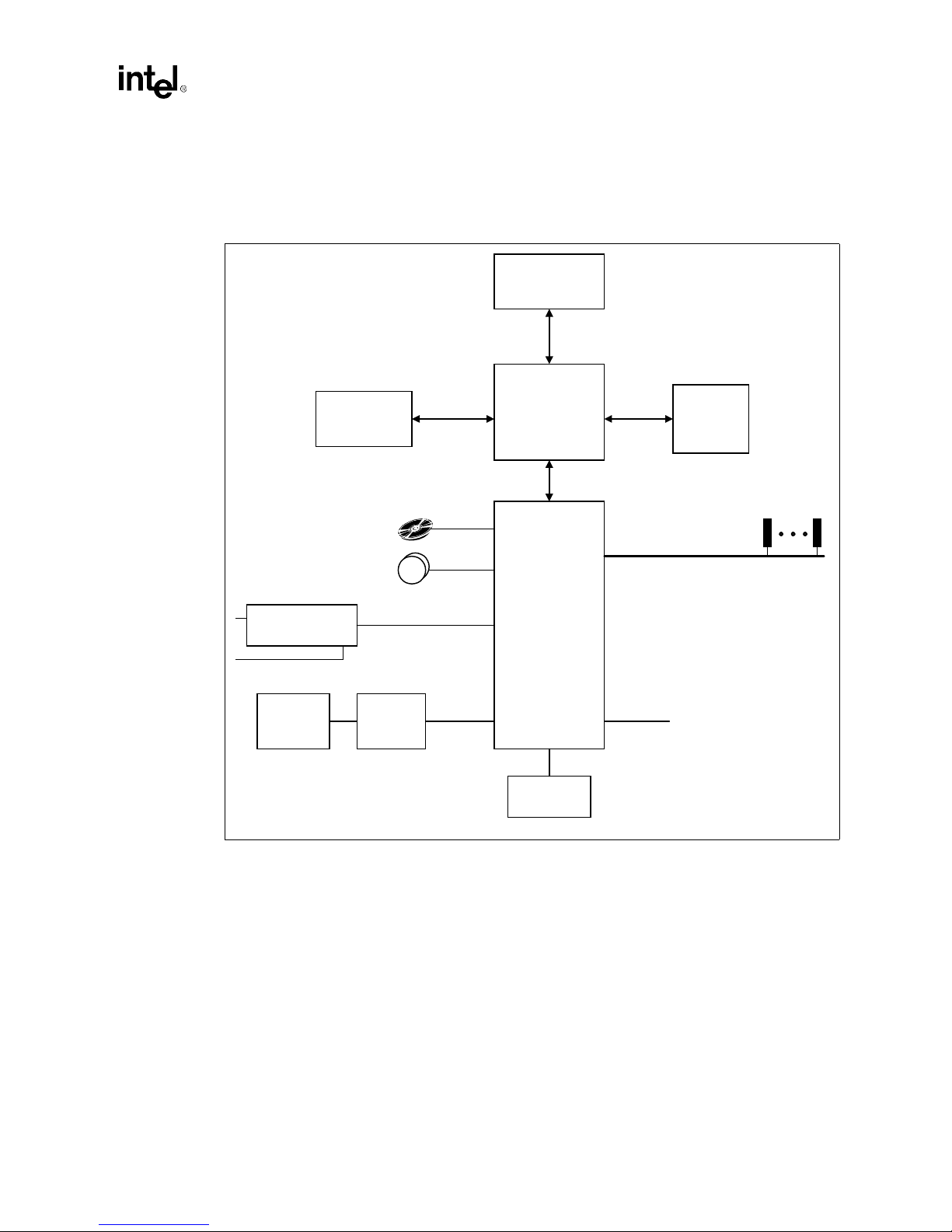
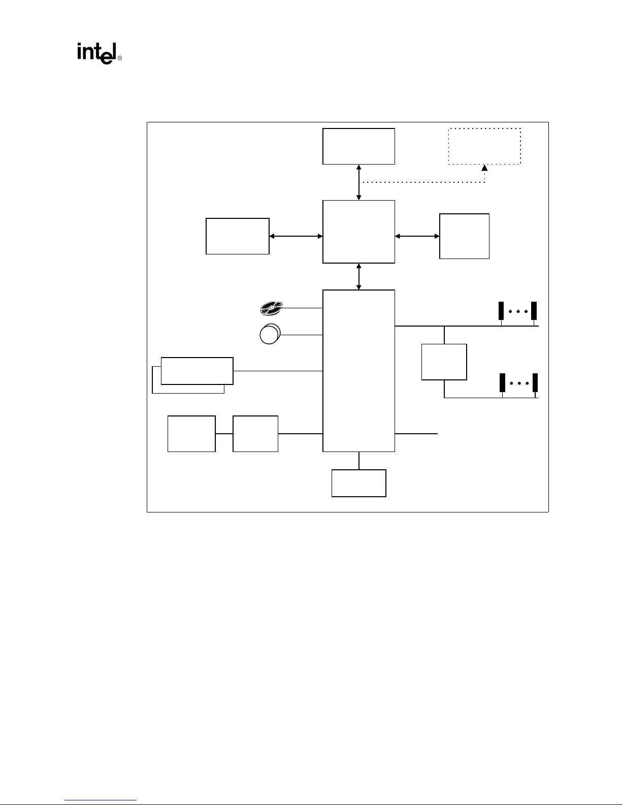
®
Figure 1-1. Intel
820 Chipset Platform Performance Desktop Block Diagram
4X AGP
Graphics
Controller
4 IDE Drives
2 USB Ports
AGP 2.0
Processor
82820
Memory
Controller Hub
(MCH)
Hub Interface
Introduction
Main
Memory
PCI Slot
PCI Bus
AC'97 Codec(s)
(optional)
Keyboard,
Mouse, FD,
PP, SP, IR
AC'97 2.1
Super I/O
82801AA
I/O Controller Hub
(ICH)
LPC I/F
GPIO
FWH Flash
BIOS
Intel®820 Chipset Design Guide 1-5
Page 18
Introduction
s
s
Figure 1-2. Intel® 820 Chipset Platform Performance Desktop Block Diagram (with ISA Bridge)
Processor
82820
4X AGP
Graphics
Controller
4 IDE Drives
2 USB Ports
AGP 2.0
Memory
Controller Hub
(MCH)
Hub Interface
Main
Memory
PCI Slot
PCI Bus
AC'97 Codec(s)
(optional)
Keyboard,
Mouse, FD,
PP, SP, IR
AC'97 2.1
Super I/O
LPC I/F
82801AA
I/O Controller Hub
(ICH)
FWH Flash
BIOS
ISA Bridge
(optional)
GPIO
ISA Slot
1-6 Intel
®
820 Chipset Design Guide
Page 19
Introduction
s
s
Figure 1-3. Intel® 820 Chipset Platform Dual-Processor Performance Desktop Block Diagram
Processor Processor
Optional 2-Way/MP
82820
4X AGP
Graphics
Controller
4 IDE Drives
2 USB Ports
AGP 2.0
Memory
Controller Hub
(MCH)
Hub Interface
Main
Memory
PCI Slot
PCI Bus
AC'97 Codec(s)
(optional)
Keyboard,
Mouse, FD,
PP, SP, IR
AC'97 2.1
Super I/O
LPC I/F
82801AA
I/O Controller Hub
(ICH)
FWH Flash
BIOS
ISA Bridge
(optional)
GPIO
ISA Slot
Intel®820 Chipset Design Guide 1-7
Page 20

Introduction
1.4 Platform Initiatives
1.4.1 Direct Rambus
The Direct Rambus* (RDRAM) initiative provides the memory bandwidth necessary to obtain
optimal performance from the Pentium III processor as well as a high-performance AGP graphics
controller. The MCH RDRAM interface supports 266 MHz, 300 MHz, 356 MHz, and 400 MH z
operation; the latter delivers 1.6 GB/s of theoretical memory bandwidth; twice the memo ry
bandwidth of 100 MHz SDRAM systems. Coupled with the greater bandwidth, the RDRAM
protocol, which is heavily pipelined, provides substantially more efficient data transfer. The
RDRAM memory interface can achieve greater than 95% utilization of the 1.6 GB/s theoretical
maximum bandwidth.
In addition to RDRAM’s performance features, the new memory architecture provides enhanced
power management capabilities. The powerdown mode of operation enables Intel
based systems to cost-effectively support suspend-to-RAM.
*
1.4.2 Streaming SIMD Extensions
The Pentium III processor provides 70 new Streaming SIMD (single instruction, multiple data)
Extensions. The Pentium III new extensions are floating point SIMD extensions . Inte l MMX™
technology provides integer SIMD extensions. The Pentium III processor new extensions
complement the Intel MMX™ technology SIMD extensions and provide a performance boost to
floating-point intensive 3D applications.
1.4.3 AGP 2.0
®
820 chipset
The AGP 2.0 interface, along with Direct Rambus* memory technology, allows graphics
controllers to access main memory at over 1 GB/s; twice the AGP bandwidth of previous AGP
platforms. AGP 2.0 provides the infrastructure necessary for photor ealistic 3D. In conjun ction with
Direct Rambus
the next level of 3D graphics performance.
*
and the Pentium III processor new Streaming SIMD Extensions, AGP 2.0 delivers
1.4.4 Hub Interface
As I/O speeds increase, the demand placed on the PCI bus by the I/O bridge has become
significant. With the addition of AC’97 and ATA/66, coupled with the existing USB, I/O
requirements will begin to impact PCI bus performance. The Intel
architecture ensures that the I/O subsystem, both PCI and the integrated I/O features (IDE, AC’97,
USB, etc.), receives adequate bandwidth. By placing the I/O bridge on the hub interface instead of
PCI, the hub architecture ensures that both the I/O functions integrated into the ICH and the PCI
peripherals obtain the bandwidth necessary for peak performance. In addition, the hub interface’s
lower pin count allows a smaller package for the MCH and ICH.
®
820 chipset’s hub interface
1-8 Intel
®
820 Chipset Design Guide
Page 21

1.4.5 Manageability
The Intel® 820 chipset platform integrates several functions designed to manage the system and
lower the total cost of ownership (TCO) of the system. These system management functions are
designed to report errors, diagn os e the s yst em, an d reco ver fro m s ystem locku ps without th e aid o f
an external microcontroller.
TCO Timer
The ICH integrates a programmable TCO T imer. This timer is used to d etect system locks. The firs t
expiration of the timer generates an SMI# which the system can use to recover from a software
lock. The second expiration of the timer causes a system reset to recover from a hardware lock.
CPU Present Indicator
The ICH looks for the CPU to fetch the first instruction after reset. If the CPU does not fetch the
first instruction, the ICH will reboot the system at the safe-mode frequency multiplier.
ECC Error Reporting
Upon detecting an ECC error, the MCH can send one of several messages to the ICH. The MCH
can instruct the ICH to generate either an SMI#, NMI#, SERR#, or TCO interrupt.
Introduction
Function Disable
The ICH provides the ability to disable the following functions: AC'97 Modem, AC'97 Audio,
IDE, USB or SMBus. Once disabled, these functions no longer decode I/O, memory, or PCI
configuration space. Also, no interrupts or power management events are generated from the
disabled functions.
Intruder Detect
The ICH provides an input signal (INTRUDER#) that can be attached to a switch that is activated
by the system case being opened. The ICH can be programmed to generate an SMI# or TCO
interrupt due to an active INTRUDER# signal.
SMBus
The ICH integrates an SMBus controller. The SMBus provides an interface to manage peripherals
(e.g., serial presence detection (SPD) on RIMMs and thermal sensors).
Alert on LAN*
The ICH supports Alert on LAN*. In response to a TCO event (intruder detect, thermal event, CPU
not booting) the ICH sends a mes sage over A LERTCLK and ALERTDAT A. A LAN contro ller can
decode this alert message and send a message over the network to alert the network manager.
Intel®820 Chipset Design Guide 1-9
Page 22

Introduction
1.4.6 AC’97
The Audio Codec’97 (AC’97) Specification defines a digital link that can be used to attach an
audio codec (AC), a modem codec (MC), an audio/modem codec (AMC), or both an AC and an
MC. The AC’97 Specification defines the interface between the system logic and the audio or
modem codec known as the AC’97 Digital Link.
The ability to add cost-effective audio and modem solutions is important as the platform migrates
away from ISA. In addition, the AC’97 audio and modem components are software configurable.
This reduces configuration errors. Intel
only replaces ISA audio and modem functionality, but also improves overall platform integration
by incorporating the AC’97 digital link. Using Intel
reduces cost and eases migration from ISA.
®
820 chipset’s AC’97 (with the appropriate codecs) not
®
820 chipset’s integrated AC’97 digital link
By using an audio codec, the AC’97 digital link allows for cost-effective, high-quality, integrated
audio on the Intel
with the use of a modem codec. Several system options exist when implementing AC’97. Intel
®
820 chipset platform. In addition, an AC’97 soft modem can be implemented
®
820 chipset’s integrated digital link allows two external codecs to be connected to the ICH. The
system designer can provide audio with an audio codec (Figure 1-4a) or a modem with a modem
codec (Figure 1-4b). For systems requiring both audio and a modem, there are two solutions. The
audio codec and the modem codec can be integrated into a single Audio Modem Codec (AMC)
(Figure 1-4c), or separate audio and modem codecs can be connected to the ICH (Figure 1-4d).
Modem implementation for different co untries mu st b e con sidered as teleph one sy stems may var y.
By using a split design, the audio codec can be on-board and the modem codec can be placed on a
riser. With a single integrated codec, or AMC, both audio and modem can be routed to a connector
near the rear panel where the external ports can be located.
The digital link in the ICH is AC’97 Rev. 2.1 compliant, supporting two codecs with independent
PCI functions for audio and modem. Microphone input and left and right audio channels are
supported for a high quality two-speaker audio solution. Wake on ring from suspend is also
supported with an appropriate modem codec.
1-10 Intel
®
820 Chipset Design Guide
Page 23
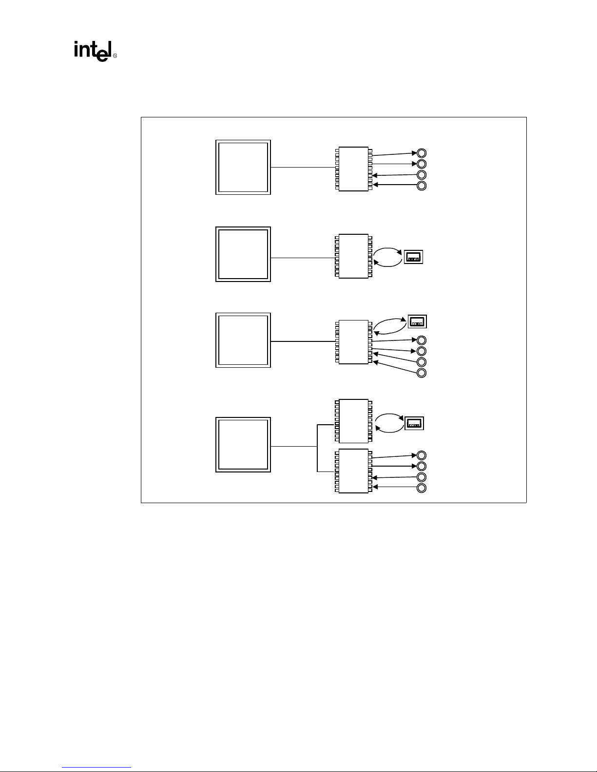
Figure 1-4. (a-d) AC’97 Connections
a) AC'97 With Audio Codec
Introduction
ICH
(241 mBGA)
b) AC'97 With Modem Codec
ICH
(241 mBGA)
c) AC'97 With Audio/Modem Codec
ICH
(241 mBGA)
d) AC'97 With Audio and Modem Codec
ICH
(241 mBGA)
AC'97 Digital
Link
AC'97 Digital
Link
AC'97 Digital
Link
AC'97
Digital Link
AC'97
Audio
Codec
AC'97
Modem
Codec
AC'97
Audio/
Modem
Codec
AC'97
Modem
Codec
AC'97
Audio
Codec
Audio Ports
Modem Port
Modem Port
Audio Ports
Modem Port
Audio Ports
1.4.7 Low Pin Count (LPC) Interface
In the Intel® 820 chipset platform, the super I/O component has migrated to the Low Pin Count
(LPC) interface. Migration to the LPC interface allows for lower cost super I/O designs. The LPC
super I/O component requires the same feature set as traditional super I/O components. It should
include a keyboard and mouse controller, floppy disk controller and serial and parallel ports. In
addition to the super I/O features, an integrated game port is recommended because the AC’97
interface does not provide support for a game port. In a system with ISA audio, the game port
typically existed on the audio card. The fifteen pin game port connect o r prov ides fo r two joys t ic ks
and a two-wire MPU-401 MIDI interface. Consult your super I/O vendor for a comprehensive list
of devices offered and features supported.
In addition, depending on system requirements, a device bay controller and USB hub could be
integrated into the LPC super I/O component. For systems requiring ISA support, an ISA-IRQ to
serial-IRQ converter is required. Potentially, this converter could be integrated into the super I/O.
Intel®820 Chipset Design Guide 1-11
Page 24

Introduction
This page is intentionally left blank
1-12 Intel
®
820 Chipset Design Guide
Page 25

Layout and Routing
Guidelines
2
Page 26

This page is intentionally left blank.
Page 27

Layout/Routing Guidelines
Layout/Routing Guidelines
This chapter documents motherboard layout and routing guidelines for Intel® 820 chipset based
systems. This section does not discuss the functional aspects of any bus, or the layout guidelines
for an add-in device.
Caution: If the guidelines listed in this document are not followed, it is very important that thorough
signal integrity and timing simulations are completed for each design. Even when the
guidelines are followed, critical signals should still be simulated to ensure proper signal integrity
and flight time. As bus speeds increase, it is imperative that the guidelines documented are
followed precisely. Any deviation from these guidelines must be simulated!
2.1 General Recommendations
The trace impedance typically noted (i.e., 60Ω ±10%) is the “nominal” trace impedance. That is,
the impedance of the trace when not subjected to the fields created by changing current in
neighboring traces. When calculating flight times, it is important to consider the minimum and
maximum impedance of a trace based on the switching of neighboring traces. Using wider spaces
between the traces can minimize this trace-to-trace coupling. In addition, these wider spaces reduce
crosstalk and settling time.
Coupling between two traces is a function of the coup led length , the d istance sep arating the traces ,
the signal edge rate, and the degree of mutual capacitance and inductance. In order to minimize the
effects of trace-to-trace coupling, the routing guidelines documented in this section should be
followed. In addition, the PCB should be fabricated as documented in Section 5.3, “Stackup
Requirement” on page 5-1 of this document.
2
All recommendations in this section (except where noted) assume 5 mil wide traces. If trace width
is greater than 5 mils then the trace spacing requirements must be adjusted accordingly (linearly).
For example, this section recommends routing most AGP signals with 5 mil traces on 20 mil spaces
(1:4). If 6 mil traces are used, then 24 mil spaces must be used (also 1:4). Using a wider trace (and
therefore wider spaces) will make routing more difficult.
Additionally, these routing guidelines are created using the stack-up described in section
Section 5.3, “Stackup Requirement” on page 5-1. If this stack-up is not used, extremely thorough
simulations of every interface must be completed. Using a thicker dielectric (prepreg) will make
routing very difficult or impossible.
2.2 Component Quadrant Layout
The quadrant layouts shown are approximate and the exact ball assignments should be used to
conduct routing analysis. These quadrant layouts are designed for use during component
placement.
Intel®820 Chipset Design Guide 2-1
Page 28
Layout/Routing Guidelines
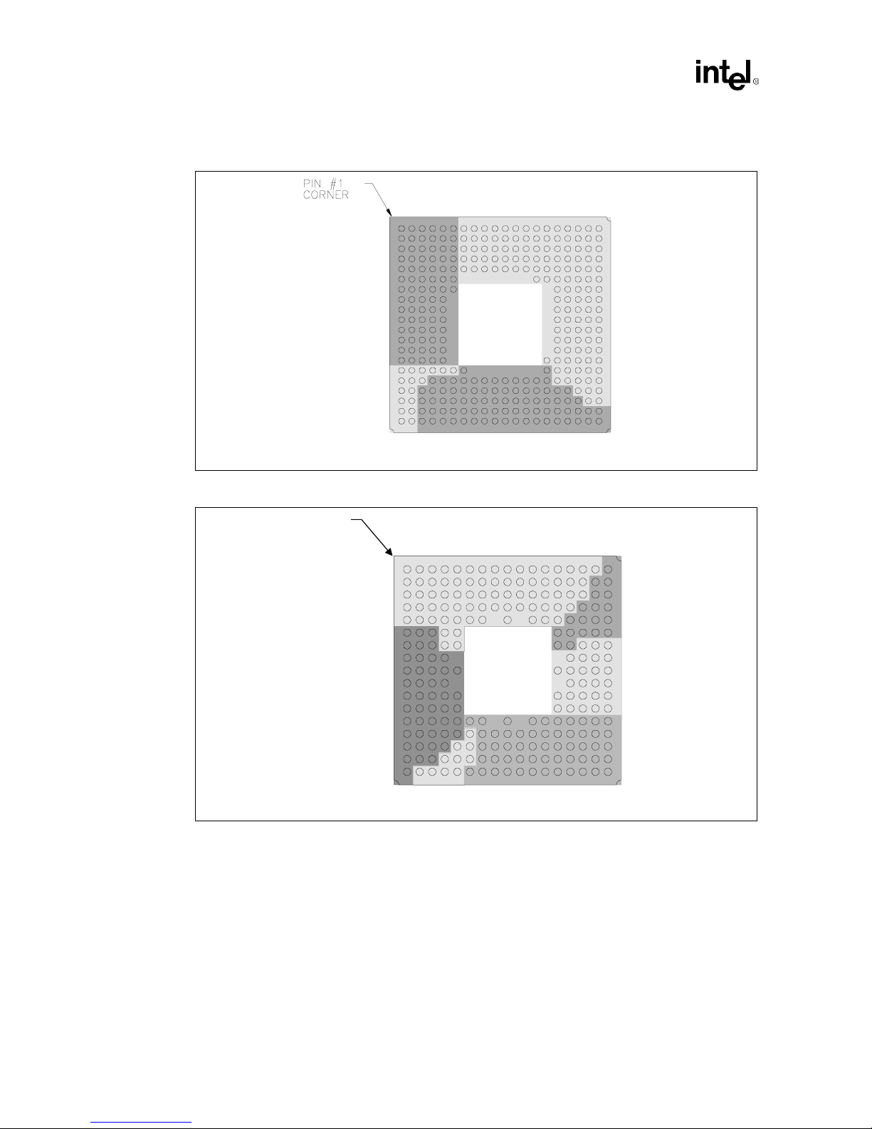
Figure 2-1. MCH 324-uBGA Quadrant Layout (Top View)
System Bus
AGP 2.0
(324-uBGA)
Hub Interface
Direct RDRAM
Figure 2-2. ICH 241-uBGA Quadrant Layout (Top View)
Pin #1 Corner
241 uBGA
AC'97,
SMBus
MCH
PCI
ICH
System Bus
Processor
Hub Interface
2-2 Intel
LPC
IDE
®
820 Chipset Design Guide
Page 29
Layout/Routing Guidelines
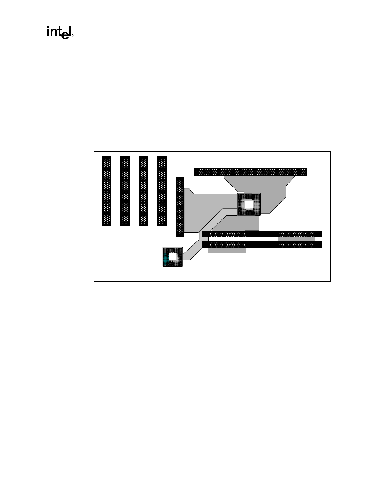
2.3 Intel® 820 Chipset Component Placement
Notes:
1.
The ATX placements and layo uts shown in
Figure 2-3 is
chipset based system design.
2. The trace length limitation between critical connections will be addressed later in this
document.
3.
The figure is for reference only.
Figure 2-3. Sample ATX MCH/ICH Component Placement
AGP
2.0
Hub Interface
ICH
RDRAM Termination
recommended for single (UP) Intel® 820
Processor Host Bus
MCH
Direct
RDRAM
Intel®820 Chipset Design Guide 2-3
Page 30
Layout/Routing Guidelines
2.4 Core Chipset Routing Recommendations
Figure 2-4 and Figure 2-5 show MCH core routing examples.
Figure 2-4. Primary Side MCH Core Routing Example (ATX)
2-4 Intel
®
820 Chipset Design Guide
Page 31

Figure 2-5. Secondary Side MCH Core Routing Example (ATX)
Layout/Routing Guidelines
2.5 Source Synchronous Strobing
Source synchronous strobing is one of the technologies used in AGP 4X, Direct RDRAM and hub
interface that allow very high data transfer rates. As buses get faster, and cycle times get shorter,
the propagation delay is becoming a limiting factor in bus speed. Source synchronous strobing is
used to minimize the impact of propagation delay (T
A source synchronous strobed interface uses strobe signals (instead of the clock) to indicate that
data is valid. Refer to Figure 2-6 for an example.
Intel®820 Chipset Design Guide 2-5
) on maximum bus frequency.
prop
Page 32

Layout/Routing Guidelines
Figure 2-6. Data Strobing Example
Clock
Strobe
Data
For a source synchronous strobed interface, it is very important that the strobe signals are routed
carefully . These signals mu st be very clean (free of noise). Data signals are typically latched on the
rising or falling edge of the strobe signal (or both). If there is noise on these signals, it could cause
an extra “edge” to be detected, thus latching incorrect data. Refer to Figure 2-7 for examples.
Figure 2-7. Effect of Crosstalk on Strobe Signal
Data
Sample
data_str.vsd
a) Correct Strobing Example (no noise) b) Effect of Crosstalk on Strobe Signal
Data is correctly
clock
Data
Threshold
Strobe
latchecd as a "0"
Some buses have more than one strobe (i.e., AGP). The AGP 1.0 specification (1X and 2X mode)
employs 3 strobe signals. These three strobe signals are each used to strobe different data signals.
That is, each strobe has an associated set of data signals. The associations for AGP 1.0 (AGP 2X)
are documented in Table 2-1. Refer to Section 2.7, “AGP 2.0” on page 2-31 for more information
on AGP 2.0 (AGP 4X, 1.5v).
T a ble 2-1. AGP 2X Data/Strobe Association
Data Associated Strobe
AD[15:0] and C/BE[1:0]# AD_STB0
AD[31:16] and C/BE[3:2]# AD_STB1
SBA[7:0] SB_STB
clock
Data
Threshold
Strobe
Data is incorrectly
latchecd as a "1"
Noise
(i.e.,
crosstalk)
In this example, the lower address signals (AD[15:0]) are sampled on the rising and falling edges
of AD_STB0, while the upper address signals (AD[31:16]) are sampled on the rising and falling
edges of AD_STB1.
2-6 Intel
®
820 Chipset Design Guide
Page 33

When routing strobes and their associated data lines, trace length mismatch is very important (in
addition to noise immunity). The primary benefit of source synchronous strobing is that the data
and the strobe arrive at the receiver simultaneously. Thus, a strobe and its associated data signals
have very critical length mismatch requirements. With well matched trace lengths (as well as
matched impedance), the propagation delay for the strobe, and the propagation delay for the data
will be very close. Hence, the strobe and the data arrive at the receiver simultaneously. For some
interfaces, the trace length mismatch requirement is less than 0.25 inch.
2.6 Direct Rambus* Interface
The Direct Rambus* Channel is a multi-symbol interconnect. Due to the length of the interconnect
and the frequency of operation, this bus is designed to allow multiple command and data packets to
be present on a signal wire at any given instant. The driving device sends the next data out before
the previous data has left the bus.
Figure 2-8. RIMM Diagram
Layout/Routing Guidelines
The nature of the multi-symbol interconnect forces many requirements on the bus design and
topology. First and foremost, a drastic reduction in reflected voltage levels is required. The
interconnect transmission lines must be terminated at their characteristic impedance, or the
reflected voltage resulting from a mismatch in impedance will degrade signal quality. These
reflections will reduce noise and timing margins, and reduce the maximum operating frequency of
the bus. Potentially, the reflections could create data errors.
Due to the tolerances of components such as PCBs, connectors, and termination resistors, there will
be some reflected voltage on the interconnect. In this multi-symbol interconnect, timings are
pattern dependent due to the reflections interfering with the next transfer.
Additionally, coupled noise can greatly affect the performance of high-speed interfaces. Just as in
source synchronous designs, the odd and even mode propagation velocity change creates skew
between the clock and data or command lines whi ch reduces t he maximu m operating frequency of
the bus. Efforts must be made to significantly decrease crosstalk, as well as the other sources of
skew.
To achieve these bus requirements, the Direct Rambus
transmission line; all components, including the individual RDRAMs, are incorporated into the
design to create a uniform bus structure that can support up to 33 devices (including the MCH)
running at 800 MegaTransfers/second (MT/s).
*
channel is designed to operate as a
Intel®820 Chipset Design Guide 2-7
Page 34

Layout/Routing Guidelines
2.6.1 Stackup
The perfect matching of transmission line impedance and un iform trace leng th are essen tial for th e
Direct RDRAM interface to work properly. Maintaining 28 Ω (±10%) loaded impedance for every
RSL (Direct Rambus* Signaling Level) signal has changed the requirements for trace width and
prepreg thickness for the Intel
on page 5-1).
Achievin g a 28 Ω nominal impedance with a traditional 7 mil prepreg requires 28 mil wide traces.
These traces are too wide to break out of the two rows of RSL balls on the MCH. To reduce trace
width, a 4.5 mil thick prepreg is required. This thinner prepreg allows 18 mil wide traces to meet
the 28 Ω (±10%) nominal impedance requirement. Refer to Section 5.3, “Stackup Requir ement” on
page 5-1 for detailed stackup requirements.
®
820 chipset platform (refer to Section 5.3, “Stackup Requirement”
2.6.2 Direct Rambus* Layout Guidelines
The signals on the Direct Rambus* Channel are broken into three groups: RSL signals, CMOS
signals, and Clocking signals. The signal groups are:
•
RSL Signals
— DQA[8:0]
—DQB[8:0]
—RQ[7:0]
•
CMOS Signals
— CMD (high-speed CMOS signal)
— SCK (high-speed CMOS signal)
—SIO
•
Clocking Signals
—CTM, CTM#
—CFM, CFM#
2.6.2.1 RSL Routing
The RSL signals enter the first RIMM on the left side, propagate through the RIMM, and exit on
the right. The signal continues through the rest of the existing RIMMs until it is terminated at
V
. All unpopulated slots must have continuity modules in place to ensure that the signals
term
propagate to the termination.
2-8 Intel
®
820 Chipset Design Guide
Page 35

Figure 2-9. RSL Routing Dimensions
MCH
To maintain a nominal 28 Ω trace impedance, the RSL signals must be 18 mils wide. To control
crosstalk and odd/even mode velocity deltas, there must be a 10 mil ground isolation trace routed
between adjacent RSL signals. The 10 mil ground isolation traces must be connected to ground
with a via every 1”. A 6 mil gap is required between the RSL signals and the ground isolation trace.
These signals must be length matched to ±10 mils in line section “A” and ±2 mils in both line
sections labeled “B” using the trace length matching methods in Section 2.6.2.6, “Length Matching
Methods” on page 2-21. T o ensure unif orm trace lines, trace width variation must be uniform on all
RSL signals at every neck-down for each line section. All RSL si gnals must hav e the same numb er
of vias. It may be necessary to place vias on RSL signals where they are not necessary to meet this
via loading requirement (i.e., dummy vias).
RIMM_0 RIMM_1
0"-3.50"
A B C
MCH to
First RIMM
0.4"-0.45"
RIMM to
RIMM
Layout/Routing Guidelines
0"-3"
RIMM to
Termination
T able 2-2. Placement Guidelines for Motherboard Routing Lengths
Reference Trace Description Maximum Trace Length (in.)
A MCH to first RIMM Connector 0” to 3.50”
B RIMM to RIMM 0.4” – 0.45”
C RIMM to Termination 0” to 3”
Figure 2-10 shows a top view of the trace width/spacing requirements for the RSL signals.
Figure 2-10. RSL Routing Diagram
18 mils
6 mils
10 mils
6 mils
18 mils
6 mils
10 mils
6 mils
Space
Space
Space
Space
RSL Signal Trace
Ground
RSL Signal Trace
Ground
Intel®820 Chipset Design Guide 2-9
Page 36

Layout/Routing Guidelines
Figure 2-11 and Figure 2-12 show a top view of an example RSL breakout and route.
Figure 2-11. Primary Side RSL Breakout Example
Ground Flood
(Shaded area)
Neckdown for BJT
BJT
Neckdown to
pass vias
18 mil clock
traces when
not 14:6
14 on 6
Differential
clock pair
2-10 Intel
®
820 Chipset Design Guide
Page 37

Figure 2-12. Secondary Side RSL Breakout Example
Layout/Routing Guidelines
2.6.2.2 RSL Termination
All RSL signals must be terminated to 1.8V (Vter m) using 2 7Ω-2% or 28Ω-1% r esistors at th e en d
of the channel opposite the MCH. Resistor packs are acceptable. Vterm must be decoupled using
high speed bypass capacitors (one 0.1 µF ceramic chip capacitor per two RSL lines) near the
terminating resistors. Additionally, bulk capacitance is required. Assuming a linear regulator with
approximate 20 ms response time, two 100 µF tantalum capacitors are recommended. The trace
length between the last RIMM and the termination resistors should be less than 3”. Length
matching in this section of the channel is not required. The Vterm power island should be at
LEAST 50 mils wide. This voltage does not need to be supplied during suspend-to-RAM.
Figure 2-13. Direct RDRAM Termination
RSL Signals
Terminator
R-packs
Vterm
Intel®820 Chipset Design Guide 2-11
Page 38

Layout/Routing Guidelines
Note: It is necessary to compensate for the slight difference in electrical characteristics between a dummy
via and a real via. Refer to Section 2.6.2.7, “VIA Compensation” on page 2-23 for more
information on Via Compensation.
Figure 2-14. Direct Rambus* Termination Example
2 GND VIAS /
Capacitor
2-12 Intel
®
820 Chipset Design Guide
Page 39

2.6.2.3 Direct Rambus* Ground Plane Reference
All RSL signals must be referenced to GND to provide an optimal current return path. The direct
Rambus ground plane reference must be continuous to the Vterm capacitors. The ground referen ce
island under the RSL signals must be continuous from the last RIMM to the back of the termination
capacitors. Choose the reference island shape such that power delivery to the components is not
compromised. The return current will flow through the Vterm capacitors into the ground island and
under the RSL traces. Any split in the ground island will provide a sub-optimal return path. In a 4
layer board, this will require the Vterm island to be on an outer layer. The Vterm island should
AL WAYS be placed on the top layer . Refer to Section 6.2, “Power Plane Splits” on page 6-7 for an
example of power plane splits.
Figure 2-15. Incorrect Direct Rambus* Ground Plane Referencing
Layout/Routing Guidelines
MCH
Wrong
1.8V Plane
RIMM1
Wrong
RIMM2
Figure 2-16. Direct Rambus Ground Plane Reference
Required
MCH
GND Plane
1.8V Plane
3.3V Plane
3.3V Plane
Extend GND PLANE
Reference Island Beyond
The ground reference island under the RSL signals MUST be connected to the ground pins on the
RIMM connector and the grou nd vias used to connect th e gr oun d is olat ion on t he 1
Intel®820 Chipset Design Guide 2-13
Vterm Capacitors
RIMM1
RIMM2
Vterm Resistors
Vterm Capacitors
Vterm Layer Not Shown
GND PlaneGND Plane
st
and 4th layers.
Page 40

Layout/Routing Guidelines
All 4 layers of the motherboard require correct grounding between the RSL signals on the
motherboard:
•
Layer 1 = Ground Isolation
•
Layer 2 = Ground Plane
•
Layer 3 = Ground Reference in the Power Plane
•
Layer 4 = Ground Isolation
All ground vias and pins MUST be connected to all 4 layers.
2.6.2.4 Direct Rambus* Connector Compensation
The RIMM connector inductance causes an impedance discontinuity on the Direct Rambus*
channel. This may reduce voltage and timing margin.
To compensate for the inductance of the connector, approximately 0.65 pF–0.85 pF compensating
capacitive tab (C-TAB) is required on each RSL connector pin. This compensating capacitance
must be added to the following connector pins at each connector:
LCTM LCTM#
RCTM RCTM#
LCFM LCFM#
RCFM RCFM#
LROW[2:0] RROW[2:0]
LCOL[4:0] RCOL[4:0]
RDQA[8:0] LDQA[8:0]
RDQB[8:0] LDQB [8:0]
SCK CMD
This can be achieved on the motherboard by adding a copper tab to the specified RSL pins at each
connector. The target value is approximately 0.65pF–0.85 pF. The copper tab area for the
recommended stackup was determined through simulation. The placement of the copper tabs can
be on any signal layer, independent of th e layer on whi ch the RSL signal is routed.
Equation is an approximation that can be used for calculating copper tab area on an outer layer.
Equation 2-1. Approximate Copper Tab Area Calculation
Length*Width = Area = C
* Thickness of prepreg / [(ε0) (εr) (1.1)]
plate
Where:
— ε
= 2.25 x 10
0
= Relative dielectric constant of prepreg material
— ε
r
-16
Farads/mil
— Thickness of prepreg = Stackup dependent
— Length, Width = Dimensions in mils of copper plate to be added
— Factor of 1.1 accounts for fringe capacitance.
Based on the stackup requirement in Section 5.3, “Stackup Requirement” on page 5-1 the copper
tab area should be 2800 to 3600 sq mils. Different stackups require different copper tab areas.
Table 2-3 shows example copper tab areas.
2-14 Intel
®
820 Chipset Design Guide
Page 41

T a ble 2-3. Copper Tab Area Calculation
Layout/Routing Guidelines
Dielectric
Thickness
(D)
4.5 6 10 6 0.65 2800
Separation
Between
Signal Trace &
Copper Tab
Minimum
Ground
flood
Air Gap
between
Signal &
GND Flood
Compen-
sating
Capacitance
in pF
Copper T ab
(C-TAB)
Area (A) In
sq mils
C-TAB
Shape
(mils)
140 L x 20 W
70 L x 40 W
Based on Equation 1, the tab area is 2800 sq mils, where εr is 4.2 and D is 4.5. These values are
based on 2116 prepreg material.
Note that more than one copper tab shape may be used. The tab dimensions are based on copper
area over the ground plane. The actual length and width of the tabs may be d ifferent due to routing
constraints (e.g., if tab must extend to center of hole, or antipad); however, each copper tab should
have equivalent area. For example, the copper tabs in Figure 2-17 have the following dimensions,
when measured tangent to the antipad:
Inner C-TAB = 140 (length) x 20(width )
Outer C-TAB = 70 (length) x 40 (width)
The following figures show a routing example of tab compensation capacitors. Note that ground
floods around the RIMM pins must not be interrupted by the capacitor tabs, and they must be
connected to avoid discontinuity in the ground plane as shown.
Intel®820 Chipset Design Guide 2-15
Page 42

Layout/Routing Guidelines
Figure 2-17. Connector Compensation Example
S
E
C
T
I
O
N
A
2-16 Intel
MCH
S
E
C
T
I
O
N
B
®
820 Chipset Design Guide
Page 43

Figure 2-18. Section A1, Top Layer
Outer C-tab
Layout/Routing Guidelines
Inner C-tab
NOTES:
1. Refe r to Figure 2-17. Ground flood removed from picture for clarity
Intel®820 Chipset Design Guide 2-17
Page 44

Layout/Routing Guidelines
Figure 2-19. Section A1, Bottom Layer
NOTES:
1. Refer to Figure 2-17. Ground flood removed from picture for clarity
2-18 Intel
®
820 Chipset Design Guide
Page 45

Figure 2-20. Section B1, Top Layer
Layout/Routing Guidelines
NOTES:
1. Refe r to Figure 2-17. Ground flood removed from picture for clarity
Intel®820 Chipset Design Guide 2-19
Page 46

Layout/Routing Guidelines
Figure 2-21. Section B
1
, Bottom Layer
NOTES:
1. Refer to Figure 2-17. Ground flood removed from picture for clarity
2.6.2.5 RSL Signal Layer Alternation
RSL signals must alternate layers as they are routed through the channel. If a signal is routed on the
primary layer from the MCH to the first RIMM socket, it must be routed on the secondary layer
from the first RIMM to the second RIMM as shown in Figure 2-22 (signal B). If a signal is routed
on the secondary layer from the MCH to the first RIMM socket, it must be routed on the primary
layer from the first RIMM to the second RIMM as shown in Figure 2-22 (signal A). Signals to the
termination resistors can be routed on either layer from the last RIMM.
2-20 Intel
®
820 Chipset Design Guide
Page 47

Figure 2-22. RSL Signal Layer Alternation
Signal on Secondary Side
Signal on Primary Side
Layout/Routing Guidelines
Signal B
Signal A
MCH
Signal B
Table 2-4. RSL Routing Layer Requirements
MCH to 1st RIMM 1st RIMM to 2nd RIMM
Method 1 Primary Side Secondary Side
Method 2 Secondar y Side Primary Side
2.6.2.6 Length Matching Methods
In order to allow for greater routing flexibility, the RSL signals require pad-to-pin length matching
between the MCH and the first connector. If the trace lengths are matched between the balls of the
MCH and the pin of RIMM connector, the length mismatch between the pad (on the die) and the
ball has not been accounted. However , gi ven the package dimension, a rep resentation o f the leng th
from the pad to the ball, the routing can compensate for this package mismatch. Therefore, the
board length mismatch can be increased.
Signal A
Route on EITHER layer.
Ground Isolation is
REQUIRED!
Term
The RSL channel requires matching trace lengths from pad-to-pin within ±10 mils.
Given these definitions:
•
Package Dimension: a representation of the length from the pad to the ball.
•
Board Trace Length: the trace length on the board.
•
Nominal RSL Length: the length to which all signals are matched. (note: there is not
necessarily a trace that is EXACTLY to nominal length, but all RSL signals must be matched
to within ±10mil of a nominal length). The Nominal RSL Length is an arbitrary length (within
the limits of the routing guidelines) to which all the RSL signals will be matched (within
10 mils).
ALL RSL signals must meet the following equation.
Intel®820 Chipset Design Guide 2-21
Page 48

Layout/Routing Guidelines
Equation 2-2. RDRAM RSL Signal Trace Length Calculation
Package Dimension + Board Trace Length = Nominal R SL Lengt h ± 10mil s
Figure 2-23. RDRAM Trace Length Matching Example
L1, L2 -> Package Dimensions
L3, L4 -> Board Trace Length
MCH Package
MCH
MCH
Die
Die
L1 + L3 = Nominal RSL Length ±10 mils
L2 + L4 = Nominal RSL Length ±10 mils
NOTE: R e fe r to the Intel
package dimensions.
L1
Ball
L2
®
820 Chipset: Intel® 82820 Memory Controller Hub (MCH) Datasheet for component
L3
L4
R
I
M
M
C
o
n
n
e
c
t
o
r
R
I
M
M
C
o
n
n
e
c
t
o
r
V
t
e
r
m
The RDRAM clocks (CTM, CTM#, CFM and CFM#) must be longer than the RDRAM signals
due to their increased trace velocity (because they are rout ed as a dif ferential pair ). To calculate the
length for each clock, the following formula should be used:
Equation 2-3. RDRAM Clock Signal Trace Length Calculation
Using this formula, the clock signals will be 21 mils/inch longer than the Nominal Length. The
lengthening of the clock signals, to compensate for their trace velocity change, ONLY applies to
routing between the MCH and the first RIMM. The clock signals should be matched in length to
the RSL signals between RIMMs. Refer to Chapter 4, “Clocking” for more detailed clock routing
guidelines.
The high-speed CMOS signals must be length matched to the RSL signals within 1200 mils
(1.2 in) due to a timing requirement between CMOS and RSL signals during NAP Exit and PDN
Exit.
It is necessary to compensate for the slight difference in electrical characteristics between a dummy
via and a real via. Refer to the following section for more information on Via Compensation.
2-22 Intel
Clock Length = Nominal RSL Signal Lengt h (package + boa rd) * 1.0 21
®
820 Chipset Design Guide
Page 49

2.6.2.7 VIA Compensation
As described in Section 2.8.2, “Strobe Signals” on page 2-44, all signals must have the same
number of vias. As a result, each trace will have 1 via (near the BGA pad) because some of the
RSL signals must be routed on the bottom of the motherboard. Therefore, it is necessary to place a
dummy via on all signals that are routed on the top layer. Because the electrical characteristics of a
dummy via do not match the electrical characteristics of a real via exactly , additional compensation
must be performed on each signal that has a dummy via. Each signal with a dummy via must have
25 mils of additional trace length. That is: a real via = a dummy via + 25 mils of trace length.
This 25 mils of additional trace length must be added to each signal routed on the top layer after
length matching, as documented in Section 2.6.2.6, “Length Matching Methods” on page2-21.
Figure 2-24. "Dummy" Via vs. Real "Via"
Layout/Routing Guidelines
“DUMMY Via”
Trace
PCB PCB
Via Via
PCB PCB
2.6.2.8 Length Matching & Via Compensation Example
Table 2-5 can be used to ensure that the RSL signals are the correct length.
Note: 2000 mils was chosen as an EXAMPLE Nominal RSL Length.
“REAL Via”
Trace
Trace
Intel®820 Chipset Design Guide 2-23
Page 50

Layout/Routing Guidelines
Table 2-5. Line Matching and Via Compensation Example
Motherboard Trace
Nominal
Signal
DQA0 A13 2000 138.14 1851.86 1871.86 1876.86 1896.86 Top
DQA1 C13 2000 19.11 1970.89 1990.89 1995.89 2015.89 Bottom
DQA2 A14 2000 163.16 1826.84 1846.84 1851.84 1871.84 Top
DQA3 C14 2000 39.87 1950.13 1970.13 1975.13 1995.13 Bottom
DQA4 B14 2000 97.54 1892.46 1912.46 1917.46 1937.46 Top
DQA5 C15 2000 62.67 1927.33 1947.33 1952.33 1972.33 Bottom
DQA6 A15 2000 186.11 1803.90 1823.90 1828.90 1848.90 Top
DQA7 C16 2000 95.70 1894.30 1914.30 1919.30 1939.30 Bottom
DQA8 A16 2000 230.20 1759.81 1779.81 1784.81 1804.81 Top
DQB0 C7 2000 39.56 1950.44 1970.44 1975.44 19 95.44 Bottom
DQB1 B7 2000 95.83 1894.17 1914.17 1919.17 1939.17 Top
DQB2 C6 2000 63.49 1926.51 1946.51 1951.51 19 71.51 Bottom
DQB3 A6 2000 153.69 1836.31 1856.31 1861.31 1881.31 Top
DQB4 C5 2000 97.33 1892.67 1912.67 1917.67 19 37.67 Bottom
DQB5 A5 2000 191.43 1798.57 1818.57 1823.57 1843.57 Top
DQB6 B5 2000 152.47 1837.53 1857.53 1862.53 1882.53 Bottom
DQB7 A4 2000 237.71 1752.29 1772.29 1777.29 1797.29 Top
DQB8 C4 2000 138.29 1851.71 1871.71 1876.71 1896.71 Bottom
RQ0 A7 2000 179.49 1810.51 1830.51 1835.51 1855.51 Top
RQ1 C8 2000 27.12 1962.88 1982.88 1987.88 2007.88 Bottom
RQ2 A8 2000 162.21 1827.79 1847.79 1852.79 1872.79 Top
RQ3 C9 2000 5.80 1984.20 2004.20 2009.20 2029.20 Bottom
RQ4 B9 2000 71.70 1918.30 1938.30 1943.30 1963.30 Top
RQ5 A9 2000 133.88 1856.12 1876.12 1881.12 1901.12 Bottom
RQ6 A10 2000 122.20 1867.81 1887.81 1892.81 1912.81 Top
RQ7 C10 2000 0.00 1990.00 2010.00 2015.00 2035.00 Bottom
CFM A12 2000 132.37 1906.85 1932.37 Bottom
CFM# B12 2000 64.63 1976.02 2001.54 Bottom
CTM B11 2000 56.06 1984.76 2010.29 Top
CTM# A11 2000 126.34 1913.01 1938.53 Top
Ball
on
MCH
RSL
Length
(mils)
Package
Dimension
(mils)
Length when
Routed on Bottom
(i.e., Real Via)
Min
(mils)
Formula A Formula B
FORMULA C FORMULA D
1,2,3,4,5,6,7,8,9,10
Motherboard Trace
Length when
Routed on Top
(i.e., Dummy Via)
Max
(mils)
Min
(mils)
Recommended
To Route On
Max
(mils)
NOTES:
1. Signals connecting to the "A" side of the RIMM connector (i.e., A1, A2, A3, etc.) should be routed on the top
(primary side) of the motherboard;
2. S ignals connecting to the "B" side of the RIMM connector should be routed on bottom (solder side).
3. These trace lengths ONLY apply from MCH to the 1st RIMM. All signals must match EXACTLY from RIMM to
RIMM.
4. Clock trace lengths include 1.021 trace velocity factor.
5. Fo rmula A min: Motherboard Trace = (Nominal RSL Length - Package Dimension) - 10 mil
6. Fo rmula A max: Motherboard Trace = (Nominal RSL Length - Package Dimension) + 10 mil
7. Fo rmula B min: Motherboard Trace = (Nominal RSL Length - Package Dimension) - 10 mil + 25 mil
8. Fo rmula B max: Motherboard Trace = (Nominal RSL Length - Package Dimension) + 10 mil + 25 mil
9. Fo rmula C: Motherboard Trace = (Nominal RSL Length - Package Dimension) * 1.021
10.Form ula D: Motherboard Trace = (Nominal RSL Length - Package Dimension + 25 mil) * 1.021
2-24 Intel
®
820 Chipset Design Guide
Page 51

2.6.3 Direct Rambus* Reference Voltage
The Direct Rambus* reference voltage (RAMREF) must be generated as shown in Figure 2-25.
RAMREF should be generated from a typical resistor divider using 2% tolerance resistors.
Additionally, RAMREF must be decoupled locally at EACH RIMM connector, at the resistor
divider and at the MCH. Finally, as shown in Figure 2-25, a 100 Ω series resistor is required near
the MCH. The RAMREF signal should be routed with a 10 mil wide trace.
Figure 2-25. RAMRef Generation Example Circuit
Vterm
MCH
R1
RAMREFA
RAMREFB
100 Ω
C4
0.1 uF 0 .1 uF
160 Ω 2%
R3
C10
R2
560 Ω 2%
Layout/Routing Guidelines
C5
0.1 uF
R
I
M
M
C8
0.1 uF
R
I
M
M
2.6.4 High-speed CMOS Routing
•
The high-speed CMOS signals (CMD & SCK) must be routed using 28 Ω traces. Using the
recommended stackup, these signals will be 18 mils wide.
•
The high-speed CMOS signals must be length matched to the RSL signals within 1200 mils
(1.2in) due to a timing requirement between CMOS and RSL signals during NAP Exit and
PDN Exit.
•
The high-speed CMOS signals require termination as shown in Figure 2-26 due to the buffer
strengths in the MCH.
•
The resistors m ust be 91 Ω pullup and 39 Ω pulldown; they also must 2% or better for S3
mode reliability. The trace impedances remain 28 Ω.
Intel®820 Chipset Design Guide 2-25
Page 52

Layout/Routing Guidelines
Figure 2-26. High-Speed CMOS Termination
MCH
RIMM_0 RIMM_1
R1
Vterm
91
Ω
2.6.4.1 SIO Routing
The SIO signal must be routed from RIMM to RIMM as shown in Figure 2-17. The SIO signal
requires a 2.2 KΩ – 10 KΩ terminating resistor on the SOUT pin of the last RIMM. SIO is routed
with a standard 5 mil wide 60 Ω trace. The motherboard routing lengths for the SIO signal are the
same as RSL signals (see Figure 2-17).
Figure 2-27. SIO Routing Example
82820
MCH
SIN B36
A
0" - 3.50"
N
3
2
1
A36 SOUT
B
0.4" - 0.45"
SIN B36
N
3
2
1
R2
A36 SOUT
39
Ω
2.2KΩ -
Ω
10K
2.6.4.2 Suspend-to-RAM Shunt Transistor
When an Intel® 820 chipset system enters or exits Suspend-to-RAM, power will be ramping to the
MCH (i.e., it will be powering-up or powerin g-down). Wh en power is ra mping, the state of the
MCH outputs is not guaranteed. Therefore, the MCH could drive the CMOS signals and issue
CMOS commands. One of the commands (the only one the RDRAMs would respond to) is the
powerdown exit command. To avoid the MCH inadvertently taking the RDRAMs out of powerdown due to the CMOS interface being driven during power ramp, the SCK (CMOS clock) signal
must be shunted to ground when the MCH is ente ring and exi ting Sus pend-t o-RAM. Thi s shunt ing
can be accomplished using the NPN transistor shown in circuit shown in Figure 2-28. The
transistor should have a Cobo of 4 pf or less (i.e., MMBT3904LT1).
In addition, to match the electrical characteristics on the SCK signal, the CMD signal needs a
dummy transistor. This transistor’s base should be tied to ground (i.e., always turned off).
2-26 Intel
®
820 Chipset Design Guide
Page 53

T o minimize impedance d iscontinuities, the traces for CMD and SCK must have a neckdown from
18 mil traces to 5 mil traces for 175 mils on either side of the SCK/CMD attach point as shown in
Figure 2-28.
Figure 2-28. RDRAM CMOS Shunt Transistor
Layout/Routing Guidelines
PWROK
MCH
MCH
18 mils
wide
VCC5SBY
2N3904
18 mils
wide
5 mils
wide
175 mils
175
mils
175 mils
5 mils
wide
18 mils
wide
R
I
M
M
S
2N3904
SCK
18 mils
wide
R
I
M
M
S
175
mils
Intel®820 Chipset Design Guide 2-27
2N3904
CMD
Page 54

Layout/Routing Guidelines
2.6.5 Direct Rambus* Clock Routing
Refer to Chapter 4, “Clocking” for Intel® 820 chipset platform Direct Rambus* clock routing
guidelines.
2.6.6 Direct Rambus* Design Checklist
Use the following checklist as a final check to ensure the motherboard incorporates solid design
practices. This list is only a reference. For correct operation, all of the design guidelines within this
document must be followed.
Table 2-6. Signal List
RSL Signals
DQA[8:0]
DQB[8:0]
RQ[7:0]
•
Ground Isolation Well Grounded
High-Speed
CMOS Signals
CMD
SCK
Serial CMOS Signal Clocks
CTM
SIO
CTM#
CFM
CFM#
— Via to ground every ½ inch around edge of isolation island
— Via to ground every ½ inch between RIMMs
— Via to ground every ½ inch between signals (from MCH to first RIMM)
— Via between every signal within 100mils of the MCH edge and the connector edge
— No unconnected ground floods
— All ground isolation at least 10 mils wide
— Ground isolation fills between serpentines
— Ground isolation not broken by C-TABs
— Ground isolation connects to the ground pins in the middle of the RIMM connectors
— Ground isolation vias connect on all 4 layers and should NOT have thermal reliefs
— Ground pins in RIMM connector connect on all 4 layers
•
Vterm Layout Yields Low Noise
— Solid Vterm island is on top layer – do not split this plane
— Ground island (for ground side of Vterm caps) is on top
— Termination Resistors connect DIRECTLY to the Vterm island on the top layer (without
vias)
— Decoupling Vterm is CRITICAL!
— Decoupling capacitors connect to top layer Vterm island and top layer ground island
directly (see layout example)
— Use AT LEAST 2 vias per decoupling capacitor in the top layer ground island
— Use 2 x 100 uF TANTALUM capacitors to decouple Vterm
(Aluminum/Electrolytic capacitors are too slow!)
— High-frequency decoupling capacitors MUST be spread-out across the term ination island
so that all termination resistors are near high-frequency capacitors
— 100uF TA NTALUM capacitors should be at each end of the Vterm island
— 100uF TA NTALUM capacitors must be connected to Vterm island directly
— 100uF TANTALUM capacitors must have AT LEAST 2 vias/cap to ground
2-28 Intel
®
820 Chipset Design Guide
Page 55

Layout/Routing Guidelines
— Vterm island should be 50 – 75 mils wide
— Vterm island should not be broken
— If any RSL signals are routed out of the last RIMM (towards termination) on the bottom
side (even for a short distance), ensure Ground Reference Plane (on the third layer) is
continuous under the termination resistors/capacitors
— Ensure current path for power delivery to the MCH does not go through the Vterm island
•
CTM/CTM# Routed Properly
— CTM/CTM# are routed differentially from DRCG to last RIMM
— CTM/CTM# are ground isolated from DRCG to last RIMM
— CTM/CTM# are ground referenced from DRCG to last RIMM
— Vias are placed in ground isolation and ground reference every ½”
— When CTM/CTM# serpentine together, they MUST maintain EXACTLY 6 mils spacing
•
Clean DRCG Power Supply
— 3.3V DRCG power flood on the top layer. This should connect to each
— High frequency (0.1 uF) capacitors are near the DRCG power pins. One capacitor next to
each power pin.
— 10uF bulk tantalum capacitor near DRCG connected directly to the 3.3V DRCG power
flood on the top layer
— Ferrite bead isolat ing D RCG power flood from 3.3V main power also connecting d irect ly
to the 3.3VDRCG power flood on the top layer
— Use 2 vias on the ground side of each
•
Good DRCG Output Network Layout
— Series resistors (39 Ω) should be VERY near CTM/CTM# pins
— Parallel resistors (51 Ω) should be very near series resistors
— CTM/CTM# should be 18mils wide from the CTM/CTM# pins to the resistors
— CTM/CTM# should be 14 on 6 routed differential as soon as possible after the resistor
network
— When not 14 on 6, the clocks should be 18 mils wide
— Ensure CTM/CTM# are ground referenced and the ground reference is connected to the
ground plane every ½” to 1”
— Ensure CTM/CTM# are ground isolated and the ground isolation is connected to the
ground plane every ½” to 1”
— Ensure 15 pf EMI capacitors to ground are removed (the pads are not necessary and
removing the pads provides more space for better placement of other components)
— Ensure the 4 pf EMI capacitor is implemented (but do not assemble the capacitor)
•
Good RSL Transmission Lines
— RSL traces are 18 mils wide
— When RSL traces neck down to exit MCH BGA, the minimum width is 15 mils and the
neckdown is no longer than 25 mils in length
— RSL traces do NOT neckdown when routing into the RIMM connector
— If tight serpentining is necessary, 10 mil ground isolation MUST be between serpentine
segments (i.e., an RSL signal CAN NOT serpentine so tightly that the si gnal is adjacent to
itself with no ground isolation between the serpentines).
— RSL traces do not cross power plane sp lits. RSL signals must also not be routed on next to
a power plane splits (e.g., the RSL signals on the 4
the ground isolation split on the 3
— Uniform ground isolation flood is exactly 6 mils from the RSL signals at all times
rd
layer)
th
layer can not be routed directly b elow
Intel®820 Chipset Design Guide 2-29
Page 56

Layout/Routing Guidelines
— ALL RSL, CMD/SCK and CTM/CTM#/CFM/CFM# signals have CTABs on each RIMM
connector pin
— All RSL signals are routed adjacent to a ground reference plane. This includes all signals
from the last RIMM to the termination. If signals are routed on the bottom from the last
RIMM to the termination, the ground reference plane on the 3
these signals AND include the ground side of the Vterm decoupling capacitors.
— CTABs must not cross (or be on top of) power plane splits. They must be ENTIRELY
referenced to ground.
— At least 10 mils ground flood isolation required around ALL RSL signals (ground
isolation must be exactly 6 mils from RSL signals). Ground flood recommended for
isolation. This ground flood should be as close to the MCH (and the 1st RIMM) as
possible. If possible connect the flood to the ground balls/pins on the MCH/connector.
•
Clean V
— Ensure 1 x 0.1 uF capacitor on V
— Use 10 mil wide trace (6 mils minimum)
— Do not route V
•
RSL Routing
— All signals must be length matched within ±10 mils of the Nominal RSL Length (note:
use the table in the Intel
to verify trace lengths). Ensure that signals with a dummy via are compensated correctly.
— ALL RSL signals must have 1 via near the MCH BGA pad. Signals routed on the
secondary side of the MB will have a “real via” while signals routed on the primary side
will have a “dummy via”. Additionally, all signals with a dummy via must have an
additional trace length of 25 mils.
— “B” side RIMM connector signals are routed on the secondary side of the motherboard.
“A” side RIMM connector signals are routed on the primary side of the motherboard.
— Signals must “alternate” layers as shown in the following table.
REF
Routing
REF
near high-speed signals
REF
®
820 chipset: 82820 Memory Controller Hub (MCH) Datasheet
at each connector
rd
layer MUST extend under
If Signal Routed from MCH to the 1st RIMM on:
Primary Side Secondary Side
Secondary Side Primary Side
•
Clock Routing
Then Route Signal fro m 1
RIMM on:
st
RIMM to Next
— Clock signals must be routed as a differential pair. The traces must be 14 mils wide and 6
mils apart (with no ground isolation) when they are routed as a differential pair. For very
short sections under the MCH and under the 1st RIMM, it will not be possible to route as
a differential pair. In these sections, the clocks signals MUST neck up to 18 mils and be
ground isolated with at least 10 mils ground isolation.
— Clock signals must be length compensated (using the 1.021 length factor described in
Section 2.7.3, “2X/4X Timing Domain Routing Guidelines” on page 2-33). Ensure that
each clock pair is length matched within ±2 mils.
— When clock signals serpentine, they must serpentine together (to maintain differential
14:6 routing).
— 22 mils ground isolation required on each side of the differential pair.
2-30 Intel
®
820 Chipset Design Guide
Page 57

2.7 AGP 2.0
For detailed AGP Interface functionality (protocols, rules and signaling mechanisms, etc.) refer to
the latest AGP Interface Specification revision 2.0, which can be obtained from http://
www.agpforum.org. This document focuses only on specific Intel
recommendations.
The AGP Interface Specification revision 2.0 enhances the functionality of the original AGP
Interface Specification (revision 1.0) by allowing 4X data transfers (4 data samples per clock) and
1.5 volt operation. In addition to these major enhancements, additional performance enhancement
and clarifications, such as fast write capability, are included in the AGP Interface Specification,
Revision 2.0. The In tel
AGP 2.0.
The 4X operation of the AGP interface provides for “quad-pumping” of the AGP AD (Address/
Data) and SBA (Side-band Addressing) buses. That is, data is sampled four times during each
66 MHz AGP clock. This means that each data cycle is ¼ of a 15 ns (66 MHz) clock or 3.75 ns. It
is important to realize that 3.75 ns is the data cycle time, not the clock cycle time. During 2X
operation, data is sampled twice during a 66 MHz clock cycle; therefore, the data cycle time is
7.5 ns.
Layout/Routing Guidelines
®
820 chipset platform
®
820 chipset is the first Intel chipset that supports the enhanced features of
To allow for these high speed data transfers, the 2X mode of AGP operation uses source
synchronous data strobing (refer to Section 2.5, “Source Synchronous Strobing” on page 2-5).
During 4X operation, the AGP interface uses differential source synchronous strobing.
With data cycle times as small as 3.75 ns, and setup/hold times of 1 ns, propagation delay
mismatch is critical. In addition to reducing propagation delay mismatch, it is important to
minimize noise. Noise on the data lines will cause the settling time to be large. If the mismatch
between a data line and the associated strobe is too great, or there is noise on the interface,
incorrect data will be sampled.
The low-voltage operation on AGP (1.5V) requires even more noise immunity. For example,
during 1.5V operation, V
is 570 mv. Without proper isolation, crosstalk could create signal
ilmax
integrity issues.
Intel®820 Chipset Design Guide 2-31
Page 58

Layout/Routing Guidelines
2.7.1 AGP Interface Signal Groups
The signals on the AGP interface are broken into three groups: 1X timing domain signals, 2X/4X
timing domain signals and miscellaneous signals. Each group has different routing requirements .
In addition, within the 2X/4X timing domain signals, there are three sets of signals. All signals in
the 2X/4X timing domain must meet minimum and maximum trace length requirements as well as
trace width and spacing requirements. However, trace length matching requirements only need to
be met within each set of 2X/4X timing domain signals.
Signal groups
•
1X Timing Domain
— CLK (3.3V)
— RBF#
—WBF#
— ST[2:0]
—PIPE#
—REQ#
—GNT#
—PAR
—FRAME#
— IRDY#
— TRDY#
—STOP#
— DEVSEL#
•
2X/4X Timing Domain
Set #1
— AD[15:0]
— C/BE[1:0]#
—AD_STB0
— AD_STB0# (used in 4X mode ONLY)
Set #2
— AD[31:16]
— C/BE[3:2]#
—AD_STB1
— AD_STB1# (used in 4X mode ONLY)
Set #3
—SBA[7:0]
—SB_STB
— SB_STB# (used in 4X mode ONLY)
•
Miscellaneous, Async
—USB+
—USB—OVRCNT#
—PME#
— TYPDET#
—PERR#
—SERR#
— INTA#
—INTB#
2-32 Intel
®
820 Chipset Design Guide
Page 59

T able 2-7. AGP 2.0 Data/Strobe Associations
Layout/Routing Guidelines
Data
AD[15:0] and
C/BE[1:0]#
AD[31:16] and
C/BE[3:2]#
SBA[7:0]
Strobes are not used in 1X mode. All data is
sampled on rising clock edges.
Strobes are not used in 1X mode. All data is
sampled on rising clock edges.
Strobes are not used in 1X mode. All data is
sampled on rising clock edges.
Associated
Strobe in 1X
AD_STB0 AD_STB0, AD_STB0#
AD_STB1 AD_STB1, AD_STB1#
SB_STB SB_STB, SB_STB#
Throughout this section the term data refers to AD[31:0], C/BE[3:0]# and SBA[7:0]. The term
strobe refers to AD_STB[1:0], AD_STB#[1:0], SB_STB and SB_STB#. When the term data is
used, it is referring to one of the three sets of data signals. When the term strobe is used, it is
referring to one of the strobes as it relates to the data in its associated group.
The routing guidelines for each group of signals (1X timing domain signals, 2X/4X timing domain
signals and miscellaneous signals) will be addressed separately.
2.7.2 1X Timing Domain Routing Guidelines
•
The AGP 1X timing domain signals (refer to Signal Groups previously shown) have a
maximum trace length of 7.5 inches. This maximum applies to ALL of the si gnals listed as 1X
timing domain signals in Signal Groups section.
•
AGP 1X timing domain signals can be routed with 5 mil minimum trace separation.
•
There are no trace length matching requirements for 1X timing domain signals.
Associated
Strobe in 2X
Associated
Strobes in 4X
2.7.3 2X/4X Timing Domain Routing Guidelines
These trace length guidelines apply to ALL of the signals listed as 2X/4X timing domain signals.
These signals should be routed using 5 mil (60 Ω) traces.
The maximum line length and length mismatch requirements are dependent on the routing rules
used on the motherboard. These routing rules were created to give design freedom by making
tradeoffs between signal coupling (trace spacing) and line lengths. The maximum length of the
AGP interface defines which set of routing guidelines must be used. Guidelines for short AGP
interfaces (e.g., < 6”) and the long AGP interfaces (e.g., > 6” and < 7.25”) are documented
separately. The maximum length allowed for the AGP interface is 7.25 inches.
Interfaces < 6”
If the AGP interface is less than 6 inches, a minimum 1:3 trace spacing is required for 2X/4X lines
(data and strobes). These 2X/4X signals must be matched their associated strobe within ±0.5
inches. These guidelines are for designs that require less than 6 inches between the AGP connector
and the MCH.
For example, if a set of strobe signals (e.g., AD_STB0 and AD_STB0#) are 5.3” long, the data
signals which are associated to those strobe signals (e.g ., AD[15:0] and C/BE[2 :0]#), can be 4.8” to
5.8” long. Another strobe set (e.g., SB_STB and SB_STB#) could be 4.2” long, and the data
signals which are associated to those strobe signals (e.g., SBA[7:0]), can be 3.7” to 4.7” long.
Intel®820 Chipset Design Guide 2-33
Page 60

Layout/Routing Guidelines
The strobe signals (AD_STB0, AD_STB0# , AD_STB1, AD_STB1#, SB_STB and SB_ST B#) act
as clocks on the source synchronous AGP interface; therefore, special care must be taken when
routing these signals. Because each strobe pair is truly a differential pair, the pair should be routed
together (e.g., AD_STB0 and AD_STB0# should be routed next to each other). The two strobes in
a strobe pair should be routed on 5 mil traces with at least 15 mils of space (1:3) between them.
This pair should be separated from the rest of the AGP signals (and all other signals) by at least
20 mils (1:4). The strobe pair must be length matched to less than ±0.1” (i.e., a strobe and its
compliment must be the same length within 0.1”).
Figure 2-29. AGP 2X/4X Routing Example for Interfaces < 6”
5 mil trace
15 mils
5 mil trace
20 mils
5 mil trace
15 mils
5 mil trace
20 mils
5 mil trace
15 mils
2X/4X Signal
2X/4X Signal
AGP STB#
AGP STB
2X/4X Signal
2X/4X Signal
Associated AGP 2X/4X Data Signal Length
Interfaces > 6” and < 7.25”
2X/4X Signal
2X/4X Signal
AGP STB#
AGP STB
2X/4X Signal
2X/4X Signal
STB/STB# Length
0.5" 0.5"
Min Max
Longer lines have more crosstalk; therefore, to reduce skew, longer line lengths require a greater
amount of spacing between traces. For line lengths greater than 6 inches and less than 7.25 inches,
1:4 routing is required for all data lines and strobes. For these designs, the line length mismatch
must be less than ±0.125” within each signal group (between all data signals and the strobe
signals).
For example, if a set of strobe signals (e.g., AD_STB0 and AD_STB0#) are 6.5” long, the data
signals which are associated with those strobe signals (e.g., AD[15:0] and C/BE[2:0]#), can be
6.475” to 6.625” long. Another strobe set (e.g., SB_STB and SB_STB#) could be 6.2” long, and
the data signals that are associated with those strobe signals (e.g., SBA[7:0]), can be 6.075” to
6.325” long.
The strobe signals (AD_STB0, AD_STB0# , AD_STB1, AD_STB1#, SB_STB and SB_ST B#) act
as clocks on the source synchronous AGP interface; therefore, special care must be taken when
routing these signals. Because each strobe pair is truly a differential pair, the pair should be routed
together (e.g., AD_STB0 and AD_STB0# should be routed next to each other). The two strobes in
a strobe pair should be routed on 5 mil traces with at least 20 mils of space (1:4) between them.
2-34 Intel
®
820 Chipset Design Guide
Page 61

This pair should be separated from the rest of the AGP signals (and all other signals) by at least
20 mils (1:4). The strobe pair must be length matched to less than ±0.1” (i.e., a strobe and its
compliment must be the same length within 0.1”).
All AGP Interfaces
The 2X/4X Timing Domain Signals can be routed with 5 mil spacing when breaking out of the
MCH. The routing must widen to the documented requirements within 0.3” of the MCH package.
When matching trace length for the AGP 4X interface, all traces should be matched from the ball
of the MCH to the pin on the AGP connector. It is not necessary to compensate for the length of the
AGP signals on the MCH package.
Reduce line length mismatch to insure added margin. In order to reduce trace to trace coupling
(cross talk), separate the traces as much as possible. All signals in a signal group should be routed
on the same layer. The trace length and trace spacing requirements must not be violated by any
signal. Trace length mismatch for all signals within a signal group should be as close to zero as
possible to provide timing margin.
2.7.4 AGP 2.0 Routing Summary
Layout/Routing Guidelines
T a ble 2-8. AGP 2.0 Routing Summary
Signal
1X Timing Domain 7.5” 5 mils
2X/4X Timing
Domain Set#1
2X/4X Timing
Domain Set#2
2X/4X Timing
Domain Set#3
2X/4X Timing
Domain Set#1
2X/4X Timing
Domain Set#2
2X/4X Timing
Domain Set#3
NOTES:
1. Each strobe pair must be separated from other signals by at least 20 mils
2. These guidelines apply to board stackups with 10% impedance tolerance
Maximum
Length
7.25” 20 mils ±0.125”
7.25” 20 mils ±0.125”
7.25” 20 mils ±0.125”
6” 15 mils
6” 15 mils
6” 15 mils
1,2
Trace Spacing
(5 mil traces)
1
1
1
Length
Mismatch
No
Requirement
±0.5”
±0.5”
±0.5”
Relative To Notes
N/A None
AD_STB0 and
AD_STB0#
AD_STB1 and
AD_STB1#
SB_STB and
SB_STB#
AD_STB0 and
AD_STB0#
AD_STB1 and
AD_STB1#
SB_STB and
SB_STB#
AD_STB0, AD_STB0#
must be the same
length
AD_STB1, AD_STB1#
must be the same
length
SB_STB, SB_STB#
must be the same
length
AD_STB0, AD_STB0#
must be the same
length
AD_STB1, AD_STB1#
must be the same
length
SB_STB, SB_STB#
must be the same
length
Intel®820 Chipset Design Guide 2-35
Page 62

Layout/Routing Guidelines
2.7.5 AGP Clock Routing
The maximum total AGP clock skew (between the MCH and the graphics component) is 1 ns for
all data transfer modes. This 1 ns includes skew and jitter which originates on the motherboard,
add-in card, and clock synthesizer. Clock skew must be evaluated not only at a single threshold
voltage, but at all points on the clock edge that fall in the switch i ng r ange. The 1 ns skew budget is
divided such that the motherboard is allotted 0.9ns of clock skew (the motherboard designer shall
determine how the 0.9 ns is allocated between the board and the synthesizer). For Intel
chipset platform AGP clock routing guidelines, refer to Chapter 4, “Clocking”.
2.7.6 General AGP Routing Guidelines
The following routing guidelines are recommended for an optimal system design. The main focus
of these guidelines is to minimize signal integrity problems on the AGP interface of the 82820
MCH. The guidelines below are not intended to replace thorough system validation on Intel
chipset based products.
Recommendations
Decoupling
®
820
®
820
•
For VDDQ decoupling, a minimum of six (6) 0.01 uF capacitors are required and at least four
(4) must be within 70 mils of the outer row of balls on the MCH. (see Figure 2-30).
•
Evenly distribute placement of decoupling capacitors among the AGP interface signal field.
•
Use a low ESL ceramic capacitor (e.g., 0603 body type, X7R dielectric).
•
In addition to the minimum decoupling capacitors, bypass capacitors should be placed at vias
that transition AGP signals from one reference signal plane to another. On a typical four layer
PCB design the signals transition from one side of the board to the other.
•
One extra 0.01 uF capacitor is required per 10 vias. The capacitor should be placed as close to
the center of the via field as possible.
•
Ensure that the AGP connector is well decoupled as described in the AGP Design Guide,
Revision 1.0 (Section 1.5.3.3).
Note: To add the decoupling capacitors close as possible to the MCH and/or close to the vias, the trace
spacing may be reduced as the traces go around each capacitor. The narrowing of space between
traces should be minimal and for as short a distance as possible (1” maximum).
2-36 Intel
®
820 Chipset Design Guide
Page 63

Figure 2-30. Top Signal Layer
Layout/Routing Guidelines
Must add six 0.01 uF ceramic 603 Type Capacitors
Ground Reference
It is strongly recommended that, at a minimum, the following critical signals be referenced to
ground from the MCH to an AGP connector (or to an AGP video controller if implemented as a
“down” solution) utilizing a minimum number of vias on each net; AD_STB0, AD_STB0#,
AD_STB1, AD_STB1#, SB_STB, SB_STB#, G_GTRY#, G_IRDY#, G_GNT# and ST[2:0].
In addition to the minimum signal set listed above, it is strongly recommended that half of all your
AGP signals be reference to ground depending on board layout. An ideal design would have the
complete AGP interface signal field referenced to ground.
The recommendations above are not specific to any particular PCB stackup, but are applied to all
®
Intel
Chipset designs.
2.7.7 VDDQ Generation and TYPEDET#
AGP specifies two separate power planes (VCC and VDDQ). VCC is the core power for the
graphics controller. VCC is always 3.3V. VDDQ is the interface voltage. In AGP 1.0
implementations VDDQ was also 3.3V. For the designer developing an AGP 1.0 motherboard,
there is no distinction between VCC and VDDQ as both are tied to the 3.3V power plane on the
motherboard.
Intel®820 Chipset Design Guide 2-37
Page 64

Layout/Routing Guidelines
AGP 2.0 requires that these power planes be separate. In conjunction with the 4X data rate, the
AGP 2.0 Interface Specification provides for low-voltage (1.5V) operation. The AGP 2.0
Specification implements a TYPEDET# (type detect) signal on the AGP connector that determines
the operating voltage of the AGP 2.0 interface (VDDQ). The motherboard must provide either
1.5V or 3.3V to the add-in card depending on the state of the TYPEDET# signal (refer to
Table 2-9. The 1.5V low-voltage operation applies ONLY to the AGP interface (VDDQ); VCC is
always 3.3V.
Note: The motherboard provides 3.3V to the Vcc pins of the AGP connector. If the graphics controller
needs a lower voltage, then the add-in card must regulate the 3.3V VCC voltage to the controller’s
requirements. The graphics controller may ONLY power AGP I/O buffers with the VDDQ power
pins.
The TYPEDET# signal indicates whether the AGP 2.0 interface operates 1.5 volts or 3.3 volts. If
TYPEDET# is floating (no connect) on an AGP add-in card, the interface is 3.3 volts. If
TYPEDET# is shorted to ground, the interface is 1.5 volts.
Table 2-9. TYPDET#/VDDQ Relationship
TYPEDET# (on add-in card) VDDQ (supplied b y MB)
GND 1.5V
N/C 3.3V
As a result of this requirement, the motherboard must provide a flexible voltage regulator. This
regulator must supply the appropriate voltage to the VDDQ pins on the AGP connector. For
specific design recommendations, refer to the schematics in Appendix A, “Reference Design
Schematics: Uni-Processor” and Appendix B, “Reference Design Schematics: Dual-Processor”.
VDDQ generation and AGP V
generation must be considered together. Before developing
REF
VDDQ generation circuitry, refer to the AGP 2.0 Interface Specification.
Figure 2-31 demonstrates one way to design the VDDQ voltage regulator. This regulator is a linear
regulator with an external, low R
FET. The source of the FET is connected to 3.3V. This
DS-ON
regulator will convert 3.3V to 1.5V or pass 3.3V depending on the state of TYPEDET#. If a linear
regulator is used, it must draw power from 3.3V (not 5V) in order to control thermals (i.e., 5V
regulated down to 1.5V with a linear regulator will dissipate approximately 7W at 2A). Because it
must draw power from 3.3V and, in some situations, must simply pass that 3.3V to VDDQ (when a
3.3V add-in card is placed in the system), the regulator MUST use a low R
AGP 1.0 modified VDDQ3.3
to 3.1V. Using an ATX power supply; the 3.3V
min
dson
FET.
is 3.168V.
min
Therefore, 68 mV of drop is allowed across the FET at 2A. This corresponds to a FET with an
R
of 34 mW.
dson
How does the regulator switch? The feedback res i stor divider is set to 1.5V. When a 1.5V card i s
placed in the system, the transistor is off and the regulator regulates to 1.5V. When a 3.3V card is
placed in the system, the transistor is on, and the feedback is pulled to grou nd. W hen this happ ens ,
the regulator drives to gate of the FET to nearly 12V. This turns the FET on and passes 3.3V - 2A *
R
DS-ON
to VDDQ.
2-38 Intel
®
820 Chipset Design Guide
Page 65

Figure 2-31. AGP VDDQ Generation Example Circuit
Layout/Routing Guidelines
TYPEDET#
1 K
+3.3V
O
+12V
O
U1
LT1575
1
SHDN IPOS
2
R1
Ω
C1
1 uF
VIN INEG
3
GND GATE
4
FB COMP
47 uF
C5
7.5 K
5
6
7
8
C4
10 pF
R5
Ω
C2
47 uF
5
Ω
R2
R3
301
R4
1.21 K
C3
220 uF
Ω
Ω
VDDQ
O
2.7.8 V
V
AGP cards generate V
down to V
GND at the MCH and graphics controller, 1.5V cards use source generated V
signal is generated at the graphics controller and sent to th e MCH, and another V
the MCH and sent to the graphics controller). Refer to Figure 2-32.
Both the graphics controller and the MCH are required to generate V
the connector (1.5V add-in cards only). There are two pins defined on the AGP 2.0 universal
connector to allow this V
To preserve the common mode relationship between the V
routing of the two Vref signals must be matched in length to the strobe lines within 0.5 inches on
the motherboard and within 0.25 inches on the add-in card.
The voltage divider networks consists of AC and DC elements as shown in the figure.
The V
benefit of the common mode power supply effects. However, the trace spacing around the V
signals must be a minimum of 25 mils to reduce cross-talk and maintain signal integrity.
Generation for AGP 2.0 (2X and 4X)
REF
generation for AGP 2.0 will be different depending on the AGP card type used. The 3.3V
REF
•
•
) as shown in Figure 2-32. To account for potential differences between VDDQ and
REF
V
GC - Vref from the graphics controller to the chipset
REF
V
CG - Vref from the chipset to the graphics controller
REF
divider network should be placed as close to the AGP interface as is practical to get the
REF
locally (i.e., they have a resistor divider on the card that divides VDDQ
REF
(i.e., the V
REF
is generated at
REF
and distribute it through
REF
passing. These pins are:
REF
and data signals, it is important the
REF
REF
REF
Intel®820 Chipset Design Guide 2-39
Page 66

Layout/Routing Guidelines
During 3.3V AGP 2.0 oper ation, V
must be 0.4VDDQ. However, during 1.5V AGP 2.0
REF
operation, Vref must be 0.5VDDQ. This requires a flexible voltage divider for V
methods of accomplishing this exist, and one such example is shown in Figure 2-32.
Figure 2-32. AGP 2.0 VREF Generation & Distribution
+12V
O
Note: R7 is the same resistor seen in
AGP VDDQ Generation Example Circuit
R7
1.5V AGP
Card
3.3V AGP
Card
AGP
Device
VDDQ
GND
REF
1K
VrefGC
VrefCG
The resistor dividers should be placed near the MCH. Both VrefGC and VrefCG
signals must be 5 mils wide and routed 25 mils from adjacent signals.
+12V
O
R7
1K
VrefGC
Figure (R1)
TYPEDET#
U6
mosfet
Note: R7 is the same resistor seen in AGP
VDDQ Generation Example Circuit Figure
(R1)
TYPEDET#
R9
300
1%
R11
200
1%
Place C10 close to the MCH
R9
300
1%
R11
200
1%
0.1uF
C10
. Various
REF
VDDQ
500pF
C8
R6
VDDQ
MCH
REF
GND
VDDQ
1K
1K
R2
500pF
C9
R5
82
R4
82
500pF
C8
VDDQ
AGP
REF
Device
GND
VrefCG
The resistor dividers should be placed near the MCH. Both VrefGC and VrefCG
The flexible V
generated V
divider shown in Figure 2-32 uses a FET switch to switch between the locally
REF
(for 3.3V add-in cards) and the source generated V
REF
Usage of the source generated V
signals must be 5 mils wide and routed 25 mils from adjacent signals.
at the receiver is optional and is a product implementation
REF
U6
mosfet
issue which is beyond the scope of this document.
Place C10 close to the MCH
0.1uF
C10
R6
VDDQ
MCH
REF
GND
(for 1.5V add-in cards).
REF
1K
R2
1K
500pF
C9
R5
82
R4
82
2-40 Intel
®
820 Chipset Design Guide
Page 67

2.7.9 Compensation
The MCH AGP interface supports resistive buffer compensation (RCOMP). Tie the GRCOMP pin
to a 40 Ω 2% (or 39 Ω 1%) pull-down resistor (to ground) via a 10 mil wide, very short (<0.5”)
trace.
2.7.10 AGP Pull-ups
AGP control signals require pull-up resistors to VDDQ on the motherboard to ensure they contain
stable values when no agent is actively driving the bus. The signals requiring pull-up resistors are:
•
1X Timing Domain Signals
—FRAME#
— TRDY#
—IRDY#
—DEVSEL#
—STOP#
—SERR#
—PERR#
—RBF#
—PIPE#
—REQ#
—WBF#
— GNT#
— ST[2:0]
It is critical that these signals are pulled up to VDDQ (NOT 3.3V).
The trace stub to the pull-up resistor on 1X timing domain signals should be kept to less than
0.5 inch to avoid signal reflections from the stub.
The strobe signals require pull-u p/pull-downs on t he motherboard to ensure th ey contain stable
values when no agent is driving the bus.
Note: INTA# and INTB# should be pulled to 3.3V – not VDDQ.
Layout/Routing Guidelines
•
2X/4X Timing Domain Signals
— AD_STB[1:0] (pull-up to VDDQ)
— SB_STB (pull-up to VDDQ)
— AD_STB[1:0]# (pull-down to ground)
— SB_STB# (pull-down to ground)
The trace stub to the pull-up/pull-down resistor on 2X/4X timing domain signals should be
kept to less than 0.1 inch to avoid signal reflections from the stub.
The pull-up/pull-down resistor value requirements are shown in the table below:
Rmin Rmax
Ω
4 K
The recommended AGP pull-up/pull-down resistor value is 8.2 KΩ.
Intel®820 Chipset Design Guide 2-41
16 K
Ω
Page 68

Layout/Routing Guidelines
2.7.10.1 AGP Signal Voltage Tolerance List
The following signals on the AGP interface are 3.3V tolerant during 1.5V operation:
•
PME#
•
INTA#
•
INTB#
•
GPERR#
•
GSERR#
•
CLK
•
RST
The following signals on the AGP interface are 5V tolerant (refer to the USB specification):
•
USB+
•
USB-
•
OVRCNT#
The following signal is a special AGP signal. It is either Grounded or No Connected on an AGP
card.
•
TYPEDET#
Note: All other signals on the AGP interface are in the VDDQ group. They are not 3.3V tolerant
during 1.5V AGP operation.
2.7.1 1 Motherboard / Add-in Card Interoperability
Currently, there are three AGP connectors:
•
3.3V AGP connector
•
1.5V AGP connector
•
Universal AGP connector.
To maximize add-in flexibility, implementing the universal connector in Intel
system is strongly recommended. All add-in cards are either 3.3V or 1.5V cards. Due to timings,
4X transfers at 3.3V are not allowed.
Table 2-10. Connector/Add-in Card Interoperability
1.5V Connector 3.3V Connector Universal Connector
1.5V Card Yes No Yes
3.3V Card No Yes Yes
®
820 chipset based
Table 2-11. Voltage/Data Rate Interoperability
1.5V VDDQ Yes Yes Yes
3.3V VDDQ Yes Yes No
2-42 Intel
1X 2X 4X
®
820 Chipset Design Guide
Page 69

2.8 Hub Interface
The MCH and ICH ball assignments have been optimized to simplify hub interface routing. It is
recommended that the hub interface signals be routed directly from th e MCH to the ICH on the top
signal layer (they do not need to be run through vias) (refer to Figure 2-4).
The hub interface is broken into two signal groups: data signals and strobe signals. These groups
are:
•
Data Signals
—HL[10:0]
•
Strobe Signals
—HL_STB
—HL_STB#
Note: HL_STB/HL_STB# is a differential strobe pair.
There are no pull-ups or pull-downs required on the hub interface.
Layout/Routing Guidelines
Each signal must be routed such that it meets the guidelines documented for the signal group to
which it belongs.
Figure 2-33. Hub Interface Signal Routing Example
1.8V
O
10 K
Ω
HL11
ICH MCH
CLK66
HL_STB
HL_STB#
HL[10:0]
GCLK
Clocks
Intel®820 Chipset Design Guide 2-43
Page 70

Layout/Routing Guidelines
2.8.1 Data Signals
The Hub interface data signals (HL[10:0]) should be routed 5 on 20 . Thes e sign als can be rou ted 5
on 15 for navigation around components or mounting holes. In order to break-out of the MCH
uBGA and the ICH uBGA, the hub interface data signals can be routed 5 on 5. The signals must be
separated to 5 on 20 within 300 mil of the uBGA package.
The maximum trace length for the hub interface data signals is 7”. These signals must each be
matched within ±0.1” of the HL_STB and HL_STB# signals.
2.8.2 Strobe Signals
Due to their differential nature, the hub inter face strobe signals should be 5 mils wide and r outed 20
mils apart. This strobe pair should be a minimum of 20 mils from any adjacent signals. The
maximum length for the strobe signals is 7” and the two strobes must be the same length.
Additionally , the trace length for each data signal must be matched to the trace length of the strobes
with ±0.1”.
2.8.3 HREF Generation/Distribution
HREF is the hub interface reference voltage. It is 0.5 * 1.8V = 0.9V ±2%. I t can be generated us ing
a single HREF divider or locally generated dividers (as shown in Figure 2-34 and Figure 2-35).
The resistors should be equal in value and rated at 1% tolerance (to maintain 2% tolerance on
0.9V). The value of these resistors must be chosen to ensure that the reference voltage tolerance is
maintained over the entire input leakage specification. The recommended range for the resistor
value is from minimum 100 ohm to maximum 1K ohm (300 ohm shown in example).
The single HREF divider should not be located more than 4" away from either MCH or ICH. If the
single HREF divider is located more than 4" away, then the locally generated hub interface
reference dividers should be used instead.
The reference voltage generated by a single HREF divider should be bypassed to ground at each
component with a 0.01 uF capacitor located close to the component HREF pin. If the reference
voltage is generated locally, the bypass capacitor needs to be close to the component HREF pin.
Figure 2-34. Single Hub Interface Reference Divider Circuit
1.8V
300
Ω
HUBREF
MCH
300
Ω
0.01uF0.01uF
HUBREF
ICH
2-44 Intel®820 Chipset Design Guide
0.1uF
HubRef1.vsd
Page 71

Figure 2-35. Locally generated Hub Interface Reference Dividers
Layout/Routing Guidelines
HUBREF
MCH
HubRef2.vsd
2.8.4 Compensation
There are two options for the ICH hub interface compensation (HLCOMP). HLCOMP is used by
the ICH to adjust buffer characteristics to specifi c board characteristics. Refer to the IC H Datasheet
for details on compensation. It can be used as either Impedance Compensation (ZCOMP) or
Resistive Compensation (RCOMP). The guidelines are below:
RCOMP: Tie the COMP pin to a 40Ω 2% (or 39 Ω 1%) pull-up resistor (to 1.8V) v ia a 10 mil
•
wide, very short (<0.5”) trace.
ZCOMP: The COMP pin must be tied to a 10 mil trace that is AT LEAST 18” long. This trace
•
must be unterminated and care should be taken when routing the signal to avoid crosstalk
(15–20 mil separation between this signal and any adjacent signals is recommended). This
signal may not cross power plane splits.
300
300
Ω
1.8V
Ω
1.8V
Ω
300
Ω
300
0.1uF 0.1uF
HUBREF
ICH
The MCH also has a hub interface compensation pin. This signal (HLCOMP) can be routed using
either the RCOMP method or ZCOMP method described for the ICH.
Intel®820 Chipset Design Guide 2-45
Page 72

Layout/Routing Guidelines
2.9 System Bus Design
2.9.1 100/133 MHz System Bus
First, determine the approximate location of the processor and the chip set on the base board. An
example topology is shown in Figure 2-36. This example “star” topology is valid for 133 MHz and
100 MHz 2-way processor/Intel
electrically in the center of the bus. The SC242 connectors should be placed on either end of the
bus to allow the processors to terminate each end.
Table 2-12 below provides segment descriptio ns and length recommendations for the investigated
topology shown in Figure 2-36. Segment lengths are defined at the pins of the devices or
components. For 2-way processor / Intel
in the unused slot when only one processor is pop ulated. This is necessary to ensure s ignal integrity
requirements are met.
Figure 2-36. Intel
®
Pentium® III Processor Dual Processor Configuration
®
820 chipset designs. The 82820 MCH should be placed
Processor Processor
®
820 chipset designs, a termination card must be placed
L1
MCH
L2
L3
L(1,2,3): Z
= 60Ω ± 15%
0
Table 2-12. Segment Descriptions and Lengths for Figure 2-36
Segment Description
L1 SC242 connector to Centerpoint 1.5 3.0
L2 SC242 connector to Centerpoint 1.5 3.0
L3 Chip set breakout stub 0.0 1.5
L1+L3 or L2+L3 SC242 distance from MCH 2.0 4.5
L1 + L2 SC242 spacing 5.5
Min length
(inches)
Figure 2-37 shows the topology and trace lengths required for single processor designs.
Figure 2-37. Intel® Pentium® III Processor Uni-Processor Configuration
Max length
(inches)
2-46 Intel®820 Chipset Design Guide
MCH Processor
L(1): Z
= 60Ω ± 15%
0
L1 Min = 1.75"
L1 Max = 4.5"
Page 73

2.9.2 System Bus Ground Plane Reference
All system bus signals must be referenced to GND to provide optimal current return path. The
ground reference must be continuous from the MCH to the SC242 connector. This may require a
GND reference island on the plane layers closest to the signals. Any split in the ground island will
provide a sub-optimal return path. In a 4 layer board, this will require the VCCID island to be on an
outer signal layer. Figure 2-38 shows a four layer motherboard power plane wit h ground reference
for system bus signals.
Figure 2-38. Ground Plane Reference (Four Layer Motherboard)
Required
SC242
GND Plane
Layout/Routing Guidelines
MCH
2.10 S.E.C.C. 2 Grounding Retention Mechanism (GRM)
Intel is enabling a new S.E.P.P. (Single Edge Processor Package) style retention mechanism which
will provide a grounding path for the heatsink on processors in the S.E.C.C. 2 package. This
solution is referred to as the S.E.C.C.2 (Single Edge Contact Cartidge 2) Grounding Retention
Mechanism (GRM). OEMs who choose to utilize this new solution will need to add grounding
pads on the primary side of the motherboard which will interface with the enabled GRM. If the
motherboard or heat sink do not have the proper interfaces, the GRM may not be utilized to its full
ability and damage could occur to the motherboard.
The most notable interface requirement to accommodate the GRM is the addition of grounding
pads around two of the Retention Mechanism (RM) mounting holes within the existing RM keepout zone on the motherboard. The other interface is a contact area on the heat sink flanges. The
interface size and locations for the motherboard are discussed in detail further in this section.
The reference design GRM is asymmetric, and requires 0.159” mounting holes. To minimize the
impact to trace routing, only two ground pads are required. This makes it necessary to key the
GRM to prevent the ground clips from being installed on the soldermask instead of the grounding
pads. This keying is accomplished by making the GRM asymmetric. The requirement for the
0.159” mounting holes is for the supported plastic fastener attachment mechanism.
Intel®820 Chipset Design Guide 2-47
Page 74

Layout/Routing Guidelines
Motherboard Interfaces
Figure 2-39 shows the Hole Locations and Keepout Zones For Support Components (from the
motherboard surface to 0.100” above the motherboard surface.).
Figure 2-39. Hole Locations and Keepout Zones For Support Components
1,2
Primary Side
1.270
0.806
0.231
4x ∅ 0.300 Keepout
Secondary Side
NOTES:
1. The dashed lin es represent the centerlines for the connector keying features.
2. Drawing not to scale
0.232
0.375
0.175
4.706
4.881
5.256
1. All dimensions are in inches and all tolerances ±0.04, unless
otherwise specified.
2. Dash lines represent control line for connector key features when
placed on planar.
3. Retention solution not to exceed height of 2.75" off of primary
side of planar and 0.150" off of secondary side of planar.
4. Retention mechanism must stay within cross-hatch area.
Figure 2-40 shows the dimensions of the grounding pad needed to ground the heat sink.
Figure 2-40. Grounding Pad Dimensions for the SECC2 GRM
0.364
0.182
4x Thru ∅ 0.159
1.038
Ground Pad Areas,
See Detail A
+0.002
-0.001
Heat Sink Area
0.232
0.464
Notes:
1. All dimensions are in inches and all
tolerances are ±0.004, unless otherwise
specified.
2. Retention mechanisim must stay within
Cross-Hatch area.
3. Entire specified plating area must be plated
Detail A
NOTE: Drawing not to scale.
and grounded with a minimum of eight VIAS.
It is not recommended to use the GRM without the minimum size ground pads in the correct
locations. If the GRM is used without the correct pads, then there is a high risk that the metal clip
that grounds to the motherboard will be t ouching the solder mask on the top layer of the bo ard, and
possibly short out traces immediately beneath the solder mask, resulting in board failure. The
required thickness of the pad is less than 0.001” (using 1/2 oz. copper).
2-48 Intel®820 Chipset Design Guide
Page 75

2.11 Processor CMOS Pullup Values
Table 2-13 contains the pullup values for the Intel® Pentium® III processor with the Intel® 820
chipset. This table supports both single and dual processor configurations.
Layout/Routing Guidelines
Table 2-13. Processor and 82820 MCH Connection Checklist
CPU Pin UP Pin Connection (CPU0) DP Pin Connection (CPU1)
AGTL+ Signals
A[35:3]#
ADS#
1
1
AERR# Leave as N/C (not supported by chipset). Leave as N/C
AP[1:0]# Leave as N/C (not supported by chipset). Leave as N/C
BERR# Leave as N/C (not supported by chipset). Leave as N/C
BINIT# Leave as N/C (not supported by chipset). Leave as N/C
1
BNR#
BP[3:2]# Leave as N/C Leave as N/C
BPM[1:0] Leave as N/C Leave as N/C
1
BPRI#
BREQ0# (BR0#) 10Ω pull down to GND See and
BREQ1# (BR1#) Leave as N/C See and
D[63:0]#
DBSY#
DEFER#
1
1
1
DEP[7:0]# Leave as N/C (not supported by chipset). Leave as N/C
1
DRDY#
1
HIT#
1
HITM#
1
LOCK#
REQ[4:0]#
RESET#
1
RP# Leave as N/C (not supported by chipset). Leave as N/C
RS[2:0]#
1
RSP# Leave as N/C (not supported by chipset). Leave as N/C
1
TRDY#
Connect A[31:3]# to MCH. Leave A[35:32]#
as N/C (not supported by chipset).
Connect to MCH Connect to 2nd processor
Connect to MCH Connect to 2nd processor
Connect to MCH Connect to 2nd processor
Connect to MCH Connect to 2nd processor
Connect to MCH Connect to 2nd processor
Connect to MCH Connect to 2nd processor
Connect to MCH Connect to 2nd processor
Connect to MCH Connect to 2nd processor
Connect to MCH Connect to 2nd processor
Connect to MCH Connect to 2nd processor
1
Connect to MCH Connect to 2nd processor
Connect to MCH, 240Ω series resistor to ITP Connect to 2nd processor
Connect to MCH Connect to 2nd processor
Connect to MCH Connect to 2nd processor
1,2
Connect A[31:3]# to 2
nd
processor
Intel®820 Chipset Design Guide 2-49
Page 76

Layout/Routing Guidelines
T able 2-13. Processor and 82820 MCH Connection Checklist
CPU Pin UP Pi n Connectio n (CP U0) DP Pin Connection (CPU1)
CMOS Signals
A20M# 150Ω pull up to Vcc2.5, connect to ICH Connect to 2
FERR# 150Ω pull up to Vcc2.5, connect to ICH Connect to 2
FLUSH# 150Ω pull up to Vcc2.5 (not used by chipset). Connect to 2
IERR#
IGNNE# 150Ω pull up to Vcc2.5, connect to ICH Connect to 2
INIT#
LINT0/INTR 150Ω pull up to Vcc2.5, connect to ICH Connect to 2
LINT1/NMI 150Ω pull up to Vcc2.5, connect to ICH Connect to 2
PICD[1:0] 150Ω pull up to Vcc2.5, connect to ICH
PREQ#
PWRGOOD
SLP# 150Ω pull up to Vcc2.5, connect to ICH
SMI# 150Ω pull up to Vcc2.5, connect to ICH
STPCLK# 150Ω pull up to Vcc2.5, connect to ICH
THERMTRIP#
TAP Signals
150Ω pull up to Vcc2.5 if tied to custom logic
or leave as N/C (not used by chipset).
150Ω pull up to Vcc2.5, connect to ICH and
FWH Flash BIOS
~200–330Ω pull up to Vcc2.5, connect to ITP
pin 16
150–330Ω pull up to 2.5V, output from the
PWRGOOD logic
150Ω pull up to Vcc2.5 and connect to power
off logic or ASIC, or leave as N/C
1,2
(Continued)
nd
processor
nd
processor
nd
processor
Connect to 2
Connect to 2
Two 300–330Ω pull ups to Vcc2.5 located
at each end of trace. Connect to 2
nd
processor
nd
processor
nd
processor
nd
processor
nd
processor
nd
processor
~200–330Ω pull up to Vcc2.5, connect to
ITP pin 20
Connect to 2
Connect to 2
nd
processor
nd
processor. Could tie
separately to a monitoring ASIC.
PRDY#
150Ω pull up to V
ITP pin 18
, 240Ω series resistor to
TT
150Ω pull up to VTT, 240Ω series resistor
to ITP pin 22
Each processor should receive a
TCK
1kΩ pull up to Vcc2.5, 47Ω series resistor to
ITP pin 5
separately buffered copy of TCK from the
ITP. Tank circuit is optional for signal
integrity. See
TDO
150Ω pull up to Vcc2.5 and connect to ITP
10
TDO of CPU1 is connected to the ITP TDO
pin 10. Pull up both sets of TDI/TDO nets
as described.
TDI of CPU0 is connected to the ITP pin 8,
TDI
~150–330Ω pull up to Vcc2.5 and connect to
ITP pin 8
TDI of CPU1 is connected to TDO of
CPU0. Pull up both sets of TDI/TDO nets
as described.
Each processor should receive a
separately buffered copy of TMS from the
ITP.
Tank circuit is optional for signal integrity.
TMS
1KΩ pull up to Vcc2.5, 47Ω series resistor
to ITP pin 7
See
nd
TRST# ~680Ω pull down, connect to ITP pin 12 Connect to 2
processor
2-50 Intel®820 Chipset Design Guide
Page 77

Layout/Routing Guidelines
Table 2-13. Processor and 82820 MCH Connection Checklist
CPU Pin UP Pin Connection (CPU0) DP Pin Connection (CPU1)
Clock Signals
Connect to CK133. 22 – 33Ω series resistor
(Though OEM needs to simulate based on
BCLK
PICCLK
Other Signals
BSEL0
BSEL1
EMI[5:1]
SLOTOCC#
TESTHI
VID[4:0]
driver characteristics). To reduce pin-to-pin
skew, tie host clock outputs together at the
clock driver then route to the MCH and
processor.
Connect to CK133. 22 – 33Ω series resistor
(Though OEM needs to simulate based on
driver characteristics)
100/133 MHz support: 220Ω pull up to 3.3V,
connected to PWRGOOD logic such that a
logic low on BSEL0 negates PWRGOOD
220Ω pull up to 3.3V, connect to CK133
SEL133/100# pin. Connect to MCH HL10 pin
via 8.2 KΩ series resistor.
Tie to GND. Zero ohm resistors are an option
instead of direct connection to GND.
Tie to GND, leave it N/C, or could be
connected to powergood logic to gate system
from powering on if no processor is present.
If used, 1 KΩ – 10 KΩ pull up to any voltage.
1K–100KΩ pull up to Vcc2.5
If a legacy design pulls this up to VCC
use a 1 KΩ – 10 KΩ pull up
CORE
Connect to on-board VR or VRM. For onboard VR, 10 KΩ pull up to power-solution
compatible voltage required (usually pulled
up to input voltage of the VR). Some of these
solutions have internal pull-ups. Optional
override (jumpers, ASIC, etc.) could be used.
May also connect to system monitoring
device.
,
1,2
(Continued)
Use separate BCLK from TAP and CPU0,
or use ganged clock. Terminate as
described.
Use separate PICCLK from CPU0.
Term inate as described.
nd
Connect to 2
Connect to 2
processor
nd
processor
Implement in same manner as CPU0.
Implement in same manner as CPU0.
Implement in same manner as CPU0.
Implement in same manner as CPU0.
CPU0 and CPU1 should have different
VR/VRMs.
Power
VCC
CORE
V
TT
No Connects
Reserved
NOTES:
1. Fo r single processo r designs, the AGTL+ bus can be dual-ended or single-ended termination based on
simulation results. Single-ended termination is provided by the processor.
2. This checklist supports Intel
a FMB guideline of 19.3A, and future Intel
Intel®820 Chipset Design Guide 2-51
Connect to core voltage regulator. Provide
high & low frequency decoupling.
Connect to 1.5V regulator. Provide high and
low frequency decoupling.
The following pins must be left as noconnects: A16, A47, A88, A113, A116, B12,
B20, B76, and B112.
®
Pentium® II processors at all current speeds, Intel® Pentium® III processors to
®
Pentium® III processors to the current FMB guideline of 18.4A.
Implement in same manner as CPU0.
Implement in same manner as CPU0.
Implement in same manner as CPU0.
Page 78

Layout/Routing Guidelines
Figure 2-41. TCK/TMS Implementation Example for DP Designs
Vcc2.5
Ω
1 K
R
I
ITP Port
TCK
or
TMS
non-inverting buffer
non-inverting buffer
100 nH
100 nH
SC242
Connector A
motherboard trace
56 pF
SC242
Connector B
motherboard trace
56 pF
Table 2-14. Bus Request Connection Scheme for DP Intel
Bus Signal Agent 0 Pins Agent 1 Pins
BREQ0# BR0# BR1#
BREQ1# BR1# BR0#
®
820 Chipset Designs
2.12 Additional Host Bus Guidelines
BREQ Pins
UP Systems: For uni-processor systems , the BREQ 0 pin sho uld b e pulle d down t o groun d thro ugh
a 10 Ω resistor. The BREQ1 pin should be left as a no-connect.
Figure 2-42. Single Processor BREQ Strapping Requirements
CPU #1
BREQ0# BREQ1#
No Connect
2-52 Intel®820 Chipset Design Guide
Page 79

DP Systems: For dual processor systems, BREQ0# (to one of the processors) needs to be driven
for arbitration ID strapping. Refer to Figure 2-43 for an example of the BREQ connections in a DP
system. It is a requirement that the on-board logic tri-state BREQ0# after the arbitration ID
strapping is complete. Additionally, BREQ0# and BREQ1# are high-speed AGTL+ signals and the
loading characteristics of the on-board logic must be considered even when the logic is tri-stated.
Figure 2-43. Dual-Processor BREQ Strapping Requirements
CPU #1 CPU #2
BREQ0# BREQ0# BREQ1#BREQ1#
on-board logic
Layout/Routing Guidelines
Figure 2-44. BREQ0# Circuitry for DP Systems
5V
R2
ΩΩΩΩ
2.7 K
CPURST#
R2
4.7 K
CPUCLK
ΩΩΩΩ
2N3904
2
/PRE
D
3
CLK CLK
/CLR
1
This circuit holds BREQ0 low for two clocks after the deas ser tion o f r eset. The 2 N390 4 co nnected
to BREQ0 should be connected to the BREQ0 AGTL trace with a very short stub. Additionally, the
series current limiting resistor on CPURESET should be attached to the CPURESET trace with a
very short stub.
External Circuit Recommendation for HA7 Strapping for IOQ Depth of 1
For debug purpose, the external logic to set the IOQ depth of 1 on the front side bus may be
needed. Do not add this circuit for production since overall system performance will be degraded.
The external logic for HA7# strapping is very similar to the BREQ0 strapping that is described in
the previous section.
5V5V
4
5
QQ
6
/Q /Q
74F74 74F74
4
2
/PRE
D
3
/CLR
1
4.7 K
5
6
BREQ0#
ΩΩΩΩ
2N3904
The timing requirement of HA7# strapping is also similar to BREQ0 strapping for the hold time
after the deassertion of RESET# (RSTIN# signal from MCH). The value of the strappin g need s to
be held for a minimum of 2 hos t clocks af ter the deassert ion of RSTIN# . Refer to the latest ver sion
of the processor datasheets for complete description on the timing requirement.
Intel®820 Chipset Design Guide 2-53
Page 80

Layout/Routing Guidelines
The recommendation for the layout and the schematic example are shown below. Layout
guidelines are:
•
Place the transistor and stub as close as possible to MCH (or place the transistor pad on top of
trace)
•
The max stub for transistor is less than 0.25”
•
The recommended loading of transistor is less than 5 pf.
•
For dual processor design, the stub is recommended to place on the stub of the MCH and as
close as possible to the MCH, and is less than 0.25”
Note: This circuit is only recommended for the debug situation that requires to set the IOQ depth equal to
1. For the production, do not add this circuit, since the overall system performance will be
degraded. Also, Intel does not guarantee the above layout recommendation will work under the
worst case condition.
Figure 2-45. HA7# Strapping Option Example Circuit (For Debug Purposes Only)
5V
5V5V
R2
2.7 K
CPURST#
R2
4.7 K
ΩΩΩΩ
ΩΩΩΩ
2N3904
4
2
D
CLK
3
5
/PRE
QQ
6
/Q /Q
/CLR
1
74F74 74F74
4
/PRE
/CLR
5
6
1
4.7 K
ΩΩΩΩ
2
D
CLK
3
jumper
R2
4.7 K
HA7
2N3904
ΩΩΩΩ
CPUCLK
In-Target Probe (ITP)
It is important that all of the processor electrical characteristic requirements are met. It is
recommended that prototype boards implement the ITP connector.
Logic Analyzer Interface (LAI)
Note that 1 KΩ resistors that are used to pull-up several processor signals in the schematics in
Appendix A, “Reference Design Schematics: Uni-Processor” and Appendix B, “Reference Design
Schematics: Dual-Processor” (e.g., HINIT#, IGNNE#, SMI#, etc.) preclude use of the Intel
Pentium III processor LAI. The Intel Pentium III processor LAI will function correctly with these
1KΩ pull-up resistors.
2-54 Intel®820 Chipset Design Guide
Page 81

Layout/Routing Guidelines
Minimizing Crosstalk on the AGTL+ Interface
The following general rules will minimize the impact of crosstalk in the high speed AGTL+ bus
design:
•
Maximize the space between traces. Maintain a minimum of 0.010” between traces wherever
possible. It may be necessary to use tighter spacings when routing between component pins.
•
Avoid parallelism between signals on adjacent layers.
•
Since AGTL+ is a low signal swing technology, it is important to isolate AGTL+ signals from
other signals by at least 0.025”. This will avoid coupling from signals that have larger voltage
swings, such as 5V PCI.
•
Select a board stack-up that minimizes the coupling between adjacent signals.
•
Route AGTL+ address, data and control signals in separate groups to minimize crosstalk
between groups. The Pentium III processor uses a split transaction bus. In a given clock cycle,
the address lines and corresponding control lines could be driven by a different agent than the
data lines and their corresponding control lines.
Additional Considerations
•
Distribute VTT with a wide trace. A 0.050” minimum trace is recommended to minimize DC
losses. Route the V
capacitors. Guidelines for V
Power Distribution Guidelines.”
trace to all components on the host bus. Be sure to include decoupling
TT
distribution and decoupling are contained in “Slot 1 Processor
TT
•
Place resistor divider pairs for V
is needed at the processor(s). V
decoupling capacitors. Guidelines for V
1 Processor Power Distribution Guidelines.”
•
Special Case AGTL+ signals for simulation: There are six AGTL+ signals that can be driven
by more than one agent simultaneously. These signals may require extra attention during the
layout and validation portions of the design. When a signal is asserted (driven low) by two
agents on the same clock edge, the two falling wave fronts will meet at some point on the bus.
This can create a large undershoot, followed by ringback which may violate the ringback
specifications. This “wired-OR” situation should be simulated for the following signals:
AERR#, BERR#, BINIT#, BNR#, HIT#, and HITM#.
generation at the MCH component. No V
REF
is generated locally on the processor. Be sure to include
REF
distribution and decoupling are contained in “Slot
REF
generation
REF
Intel®820 Chipset Design Guide 2-55
Page 82

Layout/Routing Guidelines
2.13 Ultra ATA/66
This section contains guidelines for connecting and routing the ICH IDE interface. The ICH has
two independent IDE channels. This section provides guidelines for IDE connector cabling and
motherboard design, including component and resistor placement, and signal termination for both
IDE channels. The ICH has integrated the 33
the IDE data signals running to the two ATA connectors.
The IDE interface can be routed with 5 mil traces on 5 mil spaces, and must be less than 8 inches
long (from ICH to IDE connector). Additionally, the shortest IDE signal (on a given IDE channel)
must be less than 0.5” shorter than the longest IDE signal (on that channel).
Cable
Length of cable: Each IDE cable must be equal to or less than 18 inches.
•
Capacitance: Less than 30 pF.
•
Placement: A maximum of 6 inches between drive connectors on the cable. If a single drive is
•
placed on the cable it should be placed at the end of the cable. If a second dr ive is placed on the
same cable it should be placed on the next closest connector to the end of the cable (6” away
from the end of the cable).
Grounding: Provide a direct low impedance chassis path between the motherboard ground
•
and hard disk drives.
ICH Placement: The ICH must be placed equal to or less than 8 inches from the ATA
•
connector(s).
PC99 requirement: Support Cable Select for master-slave configuration is a system design
•
requirement for Microsoft* PC99. CSEL signal needs to be pulled down at the host side by
using a 470
pull-down resistor for each ATA connector.
Ω
series resistors that have been typically required on
Ω
2.13.1 Ultra ATA/66 Detection
The Intel® 820 chipset supports many Ultra DMA modes including ATA/66. The Intel® 820
chipset needs to determine the installed IDE device mode and the type of cable to configure its own
hardware and software to support it.
A new IDE cable is required for Ultra ATA/66. This cable is an 80 conductor cable; however the 40
pin connectors do not change. The wires in the cable alternate: ground, signal, ground, signal,
ground, signal, ground… All the ground wires are tied together on the cable (and they are tied to
the ground on the motherboard through the ground pins in the 40 pin connector). This cable
conforms to the Small Form Factor Specification SFF-8049. This specification can be obtained
from the Small Form Factor Committee.
To determine if ATA/66 mode can be enabled, the Intel
attempt to determine the cable type used in the system. The BIOS does this in one of two ways:
•
Host Side Detection
•
Device Side Detection
If the BIOS detects an 80-conductor cable, it may use any Ultra DMA mode up to the highest
transfer mode supported by both the Intel
can only enable modes that do not require an 80-conductor cable (e.g., Ultra ATA/33 Mode).
After determining the Ultra DMA mode to be used, the BIOS will configure the Intel
hardware and software to match the selected mode.
®
820 chipset requires the system BIOS to
®
820 chipset and the IDE device. Otherwise, the BIOS
®
820 chipset
2-56 Intel®820 Chipset Design Guide
Page 83

2.13.2 Ultra ATA/66 Cable Detection
The Intel® 820 chipset can use two methods to detect the cable type. Each mode requires a
different motherboard layout.
Host-Side Detection (BIOS Detects Cable Type Using GPIOs)
Host side detection requires the use of two GPI pins (1 per IDE controller). The proper way to
connect the PDIAG/CBLID signal of the IDE connector to the host is shown in Figure 2-46. All
IDE devices have a 10 KΩ pull-up resistor to 5 volts. The GPI and GPIO pi ns on t he ICH and GPI
pins on the FWH Flash BIOS are not 5 volt tolerant. This requires a resistor divider so that 5 volts
will not be driven to the ICH or FWH Flash BIOS pins. The proper value of the series resistor is
15 KΩ (as shown in Figure 2-46). This creates a 10 KΩ / 15 KΩ resistor divider and produces
approximately 3 volts for a logic high.
This mechanism allows the host, after diagnostics, to sample PDIAG/CBLID. If PDIAG/CBLIB is
high then there is 40-conductor cable in the s ystem and ATA modes 3 and 4 should not be enabled.
If PDIAG/CBLID is low then there is an 80-conductor cable in the system.
Figure 2-46. Host-Side IDE Cable Detection
Layout/Routing Guidelines
IDE Drive
ICH
ICH
GPIO
GPIO
GPIO
GPIO
To Secondary
IDE Connector
15 K
To Secondary
IDE Connector
15 K
5V
10 K
5V
PDIAG
IDE Drive
10 K
PDIAG
Ω
Ω
40-Conductor
Cable
Ω
80-Conductor
IDE Cable
Ω
Open
Intel®820 Chipset Design Guide 2-57
Page 84

Layout/Routing Guidelines
Device-Side Detection (BIOS Queries IDE Drive for Cable Type)
Device side detection requires only a 0.047 uF capacitor on the motherboard as shown in
Figure 2-47. This mechanism creates a resistor-capacitor (RC) time con stant. The AT A mode 3 or 4
drive will drive PDIAG/CBLID low and then release it (pulled up through a 10 KΩ resistor) The
drive will sample the PDIAG signal after releasing it. In an 80-conductor cable, PDIAG/CBLID is
not connected through and, therefore, the capacitor has no effect. In a 40-conductor cable, PDIAG/
CBLID is connected though to the drive. Therefore, the signal rises more slowly. The drive can
detect the difference in rise times and it reports the cable type to the BIOS when it sends the
IDENTIFY_DEVICE packet during system boot as described in the ATA/66 specification.
Figure 2-47. Drive-Side IDE Cable Detect ion
40-Conductor
Cable
5V
10 K
IDE Drive
Ω
ICH
ICH
0.047 uF
0.047 uF
80-Conductor
IDE Cable
Open
5V
PDIAG
10 K
PDIAG
IDE Drive
Ω
Layout for BOTH Host-Side and Drive-Side Cable Detection
It is possible to layout fo r bo th Hos t-Si d e and D r ive-S i de cable detection and decide the method to
be used during assembly. Figure 2-48 shows the layout that allows for both host-side and drive-side
detection.
•
For Host-Side Detection:
—R1 is a 0Ω resistor
—R2 is a 15KΩ re sistor
— C1 is not stuffed
•
For Drive-Side Detection:
— R1 is not stuffed
— R2 is not stuffed
— C1 is a 0.047 uF capacitor
2-58 Intel®820 Chipset Design Guide
Page 85

Figure 2-48. Layout for Host- or Drive-Side IDE Cable Detection
Layout/Routing Guidelines
Figure 2-49. Ultra ATA/66 Cable
ICH
R2
R1
C1
IDE Connector
Intel®820 Chipset Design Guide 2-59
Black wires are ground
Grey wires are signals
Page 86

Layout/Routing Guidelines
2.13.3 Ultra ATA/66 Pullup/Pulldown Requirements
•
22 Ω – 47 Ω series resistors are required on RESET#. The correct value sho uld be determined
for each unique motherboard design, based on signal quality.
•
An 8.2 KΩ to 10 KΩ pull-up resistor is required on IRQ14 and IRQ15 to VCC5.
•
A 10 KΩ pull-down resistor is required on PDD7 and SDD7 (as required by the ATA-4
specification).
•
A 5.6 KΩ pull-down resistor is required on PDDREQ# and SDDREQ# (as required by the
ATA-4 specification).
•
A 1K Ω pull-up resistor is required on PIORDY and SIORDY (as required by the ATA-4
specification).
Figure 2-50. Resistor Requirements for Primary IDE Connector
PCIRST_BUF#*
PDD[15:8]
PDD[7]
PDD[6:0]
PDA[2:0]
PDCS1#
PDCS3#
PDIOR#
PDIOW#
PDDREQ
PIORDY
IRQ14
PDDACK#
ICH
*Due to ringing, PCIRST# must be buffered.
1k
ohm
5V
8.2k-10k
ohm
5V
5.6k
ohm
22 - 47 ohm
10k
ohm
470 ohm
N.C.
N.C.
Reset#
Primary IDE Connector
CSEL
Pin 32
Pin 34
2-60 Intel®820 Chipset Design Guide
Page 87

Figure 2-51. Resistor Requirements for Secondary IDE Connector
Layout/Routing Guidelines
PCIRST_BUF#*
SDD[15:8]
SDD[7]
SDD[6:0]
SDA[2:0]
SDCS1#
SDCS3#
SDIOR#
SDIOW#
SDDREQ
SIORDY
IRQ15
SDDACK#
ICH
*Due to ringing, PCIRST# must be buffered.
1k
ohm
5V
8.2k-10k
ohm
5V
5.6k
ohm
22 - 47 ohm
10k
ohm
470 ohm
N.C.
N.C.
Reset#
Secondary IDE Connector
CSEL
Pin 32
Pin 34
2.14 AC’97
The ICH implements an AC’97 2.1 compliant digital controller. Any codec attached to the ICH
AC-link must be AC’97 2.1 compliant as well. Contact your codec IHV for information on 2.1
compliant products. The AC’97 2.1 specification is on the Intel website. The ICH supports the
following combinations of codecs:
Table 2-15. ICH Codec Options
Audio (AC) None
Modem (MC) None
Audio (AC) Modem (MC)
Audio/Modem (AMC) None
As shown in the table, the ICH does not support two codecs of the same type on the link. For
example, if an AMC is on the link, it must be the only codec. If an AC is on the link, another AC
cannot be present.
Intel has developed a common connector specification known as the Audio/Modem Riser (AMR).
This specification defines a mechanism for allowing OEM plug-in card options.
Primary Secondary
Intel®820 Chipset Design Guide 2-61
Page 88

Layout/Routing Guidelines
The AMR specification provides a mechanism for AC’97 codecs to be on a riser card. This is
important for modem codecs as it helps ease international certification of the modem.
For increased part placement flexibility, there are two routing methods for the AC’97 interface: the
tee topology and the daisy-chain topology. The AC’97 interface can be routed using 5 mil traces
with 5 mil space between the traces.
Figure 2-52. Tee Topology AC'97 Trace Length Requirements
4" Max
Codec
ICH
2" Max 3" Max
A
M
R
Figure 2-53. Daisy-Chain Topology AC'97 Trace Length Requirements
ICH Codec
5" Max
A
M
R
3" Max
2-62 Intel®820 Chipset Design Guide
Page 89

Layout/Routing Guidelines
Clocking is provided from the primary codec on the link via BITCLK, and is derived from a
24.576 MHz crystal or oscillator. Refer to the primary codec vendor for crystal or oscillator
requirements. BITCLK is a 12.288 MHz clock driven by the primary codec to the digital controller
(ICH), and any other codec present. That clock is used as the timebase for latching and driving
data.
On the Intel
®
820 chipset platform, the ICH supports Wake on Ring from S1, S3, and S4 via the
AC’97 link. The codec asserts SDATAIN to wake the system. To provide wake capability and/or
caller ID, standby power must be provided to the modem codec.
The ICH has weak pulldowns/pullups that are only enabled when the AC-Link Shut Off bit in the
ICH is set. This will keep the link from floating when the AC-link is off, or there are no codecs
present.
If the Shut-off bit is not set, it implies that there is a codec on the link. Therefore, BITCLK and
AC_SDOUT will be driven by the codec and ICH respectively. However, AC_SDIN0 and
AC_SDIN1 may not be driven. If the link is enabled, the assumption can be made that there is at
least one codec. If there is an onboard codec only (i.e., no AMR), then the un used SDIN p in should
have a weak (10 KΩ) pulldown to keep it from floating. If an AMR is used, any SDIN signal that
could be no connected (e.g., with no codec, both can be NC), then both SDIN pins must have a
10 KΩ pulldown.
T able 2-16. AC'97 SDIN Pulldown Resistors
System Solution Pullup Requirements
On-board Codec Only Pulldown the SDIN pin that is NOT connected to the codec
AMR Only Pulldown BOTH SDIN pins
BOTH AMR and On-board Codec Pulldown any SDIN pin that could be NC*
NOTE: If the on-board codec can be disabled, both SDIN pins must have pulldowns. If the on-board codec can
not be disabled, only the SDIN not connected to the on-board codec requires a pulldown.
2.14.1 AC’97 Signal Quality Requirements
In a lightly loaded system (e.g., single codec down), AC'97 signal integrity should be evaluated to
confirm that the signal quality on the link is acceptable to the codec used in the design. A series
resistor at the driver and a capacitor at the codec can be implemented in order to compensate for
any signal integrity issues. The values used will be design dependent and should be verified for
correct timings. The ICH AC-link output buffers are designed to meet the AC'97 2.1 specification
with the specified load of 50pF.
2.14.2 AC’97 Motherboard Implementation
The following design considerations are provided fo r the implementation of an ICH0/ICH platform
using AC’97. These design guidelines have been developed to ensure maximum flexibility for
board designers while reducing the risk of board related issues. These recommendations do not
represent the only implementation or a complete checklist, but provides recommendations based on
the ICH0/ICH platform.
Intel®820 Chipset Design Guide 2-63
Page 90

Layout/Routing Guidelines
•
Codec Implementation
— The motherboard can implement any valid combination of codecs on the mother board and
on the riser. For ease of homologation, it is recommended that a modem codec be
implemented on the AMR module; however, nothing precludes a modem codec on the
motherboard.
— Only one primary codec can be pr esent on the link. A max imum of two pres ent codecs can
be supported in an ICH0/ICH platform.
— If the motherboard implements an active primary codec on the motherboard and provides
an AMR connector, it must tie PRI_DN# to ground.
— The PRI_DN# pin is provided to indicate a primary codec is present on the motherboard.
Therefore, the AMR module and/or codec must provide a means to prevent contention
when this signal is asserted by the motherboard, without software intervention.
— Components (e.g., FET switches), buffers, or logic states should not be implemented on
the AC-link signals, except for AC_RST#. Doing so will potentially interfere with timing
margins and signal integrity.
— If the motherboard requires that an AMR module over ride a primary codec d own, a means
of preventing contention on the AC-link must be provided for the onboard codec.
— The ICH0/ICH supports Wake on Ring* from S1-S4 states via the AC’97 link. The codec
asserts SDATAIN to wake the system. To provide wake capability and/or caller ID,
standby power must be provided to the modem codec. If no codec is attached to the link,
internal pulldowns will prevent the inputs from floating, therefore external resistors are
not required. The ICH0/ICH does not wake from the S5 state via the AC’97 link.
— The SDATAIN[0:1] pins should no t be left in a floating state if the pins are n ot connected
and the AC-link is active—they should be pulled to ground through a weak
(approximately 10 KΩ) pull-down resistor. If the AC-link is disabled (by setting the shutoff bit to 1), then the ICH0/ICH’s internal pull-down resistors are enabled, and thus there
is no need for external pull-down resistors. However, if the AC-link is to be active, then
there should be pull-down resistors on any SDATAIN signal that has the potential of not
being connected to a codec. For example, if a dedicated audio codec is on the
motherboard, and cannot be disabled via a hardware jumper or stuffing option, then its
SDATAIN s ignal does not n eed a pul l-down resistor. If however, the SD ATAIN signal has
no codec connected, or is connected to an AMR slot, or is connected to an onboard codec
that can be hardware disabled, then the signal should have an external pull-down resistor
to ground.
•
AMR Slot Special Connections
— AUDIO_MUTE#: No connect on the motherboard.
— AUDIO_PWRDN: No connect on the motherboard. Codecs on the AMR card should
implement a powerdown pin, per the AC’97 2.1 specification, to control the amplifier.
— MONO_PHONE: Connect top onboard audio codec if supported.
— MONO_OUT/PC_BEEP: Connect to SPKR output from the ICH0/ICH, or MONO_OUT
from onboard codec.
— PRIMARY_DN#: See discussion above.
— +5VDUAL/+5VSB: Connect to VCC5 core on the motherboard, unless adequate power
supply is available. An AMR card using this standby/dual supply should not prevent basic
operation if this pin is connected to core power.
— S/P-DIF_IN: Connect to ground on the motherboard.
— AC_SDATAIN[3:2]: No connect on the motherboard. The ICH0/ICH supports a
maximum of two codecs, which should be attached to SDATAIN[1:0].
— AC97_MSTRCLK: Connect to ground on the motherboard.
•
The ICH0/ICH provides internal weak pulldowns. Therefore, the motherboard does not need
to provide discrete pulldown resistors.
•
PC_BEEP should be routed through the audio codec. Care should be taken to avoid the
introduction of a pop when powering the mixer up or down.
2-64 Intel®820 Chipset Design Guide
Page 91

2.15 USB
The following are general guidelines for the USB interface:
•
Unused USB ports should be terminated with 15 KΩ pulldown resistors on both P+/P- data
lines.
•
15 Ω series resistors should be placed as close as possible to the ICH (<1 inch). These series
resistors are required for source termination of the reflected signal.
•
47 pF caps must be placed as close to the ICH as possible and on the ICH side of the series
resistors on the USB data lines (P0+/-, P1+/-). These caps are there for signal quality (rise/fall
time) and to help minimize EMI radiation.
•
15 KΩ ±5% pulldown resistors should be placed on the USB side of the series resisto rs on the
USB data lines (P0+/-, P1+/-), and are REQUIRED for signal termination by USB
specification. The length of the stub should be as short as possible.
•
The trace impedance for the P0+/-, P1+/- signals should be 45 Ω (to ground) for each USB
signal P+ or P-. Using the stackup recommended in section Section 5.3, “Stackup
Requirement” on page 5-1. USB requires 9 mils traces. The impedance is 90 Ω between the
differential signal pairs P+ and P- to match the 90 Ω USB twisted pair cable impedance. Note
that twisted pair characteristic impedance of 90Ω is the series impedance of both wires,
resulting in an individual wire presenting a 45 Ω impedance. The trace impedance can be
controlled by carefully selecting the trace width, trace distance from power or ground planes,
and physical proximity of nearby traces.
•
USB data lines must be ro uted as cri tical signals. Th e P+/P- sig nal pair mus t be routed together
and not parallel with other signal traces to minimize crosstalk. Doubling the space from the
P+/P- signal pair to adjacent signal traces will help to prevent crosstalk. Do not worry about
crosstalk between the two P+/P- signal traces. The P+/P- signal traces must also be the same
length. This will minimize the effect of common mode current on EMI.
Layout/Routing Guidelines
Figure 2-54 illustrates the recommended USB schematic.
Figure 2-54. USB Data Signals
Driver
P+
Driver
P-
ICH
< 1"
< 1"
15 ohm
47 pf
15 ohm
47 pf
Motherboard Trace
45 ohm
15k
90 ohm
Motherboard Trace
USB Connector
45 ohm
15k
USB Twisted Pair CableTransmission Line
Intel®820 Chipset Design Guide 2-65
Page 92

Layout/Routing Guidelines
Recommended USB trace characteristics
•
Impedance ‘Z0’ = 45.4 Ω
•
Line Delay = 160.2 ps
•
Capacitance = 3.5 pF
•
Inductance = 7.3 nH
•
Res @ 20° C = 53.9 mOhm
2.16 ISA (82380AB)
2.16.1 ICH GPIO connected to 82380AB
At reset, the ICH LPC Br idge defau lts to subtract ive deco de. Since the LPC bridge logicall y sits on
PCI there will be two subtractive decode bridges in systems with the 82380AB (which is also a
subtractive decode device). A GPO that defaults high (i.e., ICH GPO 21) must be connected to the
NOGO signal on the 82380AB. Asserting NOGO prevents the 82380AB from subtractively
decoding cycles on the PCI bus. The BIOS must configure the 82380AB, program the ICH to
positively decode LPC cycles, and release the NOGO signal to the 82380AB.
2.16.2 Sub Class Code
Both the LPC Bridge and the 82380AB have the same Sub Class code indicating an ISA bridge.
This can not be handled by the OS’s PC I PnP code. The ICH provides the ability to hide IDSEL to
the 82380AB. ICH A22 must be connected to the 82380AB IDSEL signal. After the BIOS
configures the 82380AB, it will set a bit in the ICH that hides the 82380AB from the OS by not
asserting the IDSEL (A22) to the 82380AB during OS enumeration.
2.17 IOAPIC Design Recommendation
UP systems not using the IOAPIC should follow these recommendations:
•
On the ICH
— Connect PICCLK directly to ground
— Connect PICD0, PICD1 to ground through a 10 KΩ resistor
•
On the CPU
— PICCLK must be connected from the clock generato r to the PICCLK pi n on the pr oces sor
— Connect PICD0 to 2.5V through 10 KΩ resistors
— Connect PICD1 to 2.5V through 10 KΩ resistors
2-66 Intel®820 Chipset Design Guide
Page 93

2.18 SMBus/Alert Bus
The Alert on LAN* signals can be used as:
Alert on LAN* signals: 4.7 KΩ pullup resistors to 3.3VSB are required.
•
GPIOs: Pullup resistors to 3.3VSB and the signals must be allowed to
•
Not Used: 4.7 KΩ pullup resistors to 3.3VSB are required.
•
If the SMBus is used only for the three SPD EEPROMs (one on each RIMM), both signals should
be pulled up with a 4.7 KΩ resistor to 3.3V.
2.19 PCI
The ICH provides a PCI Bus interface that is compliant with the PCI Local Bus Specification
Revision 2.2. The implementation is optimized for high-performance data streaming when the ICH
is acting as either the target or the initiator on the PCI bus. For more information on the PCI Bus
interface, refer to the PCI Local Bus Specification Revision 2.2.
Layout/Routing Guidelines
change states on powerup (e.g., on power-up, the ICH drives
heartbeat m e ssages until the BIOS programs these signals as
GPIOs). The value of t he pullup res istors depends on the loading on
the GPIO signal.
The ICH supports six PCI Bus masters (excluding the ICH), by providing six REQ#/GNT# pairs.
In addition, the ICH supports two PC/PCI REQ#/GNT# pairs, one of which is multiplexed with a
PCI REQ#/GNT# pair.
Figure 2-55. PCI Bus Layout Example
2.20 RTC
The ICH contains a real time clock (RTC) with 256 bytes of battery backed SRAM. The internal
RTC module provides two key functions: keeping date and t ime, and storing system data in its
RAM when the system is powered down.
This section will present the recommended hookup for th e RTC circuit for the ICH. This circuit is
not the same as the circuit used for the PIIX4.
ICH
Intel®820 Chipset Design Guide 2-67
Page 94

Layout/Routing Guidelines
2.20.1 RTC Crystal
The ICH RTC module requires an external oscillating source of 32.768 KHz connected on the
RTCX1 and RTCX2 pins. Figure 2-56 documents the external circuitry that comprises the
oscillator of the ICH RTC.
Figure 2-56. External Circuitry for the ICH RTC
2
VCC3_3SBY
Vbat_rtc
Ω
1 k
Ω
1 k
0.047 uF
C1
32768 Hz
Xtal
1 µF
C2
1
C3
1
R1
10 M
R2
10 M
Ω
Ω
VCCRTC
RTCX2
RTCX1
VBIAS
7
VSS
NOTES:
1. The exact capacitor value needs to based on what the crystal maker recommends.
2. T his circu it is not the same as the one used for PIIX4.
3. V CC
4. RTCX2: Crystal Input 2 – Connected to the 32.768 KHz crystal.
: Power for RTC Well
RTC
5. RTCX1: Crystal Input 1 – Connected to the 32.768 KHz crystal.
6. VBIAS: RTC BIAS Voltage – This pin is used to provide a reference voltage, and this DC voltage sets a
current which is mirrored throughout the oscillator and buffer circuitry.
7. VS S: Groun d
3
4
5
6
2.20.2 External Capacitors
To maintain the RTC accuracy, the external capacitor C1 needs to be 0.047 uF, and the external
capacitor values (C2 and C3) should be chosen to provide the manufacturer’s specified load
capacitance (Cload) for the crystal when combined with the parasitic capacitance of the trace,
socket (if used), and package. When the external capacitor values are combined with the
capacitance of the trace, socket, and package, the closer the capacitor value can be matched to the
actual load capacitance of the crystal used, the more accurate the RTC will be.
Equation 2-4 can be used to choose the external capacitance values (C2 and C3):
Equation 2-4. External Capacitance Calculation
Cload = (C2 * C3)/(C2 +C3) + Cp arasitic
C3 can be chosen such that C3 > C2. Then C2 can be trimmed to obtain the 32.768 kHz.
2-68 Intel®820 Chipset Design Guide
Page 95

2.20.3 RTC Layout Considerations
•
Keep the RTC lead lengths as short as possible; around ¼ inch is sufficient.
•
Minimize the capacitance between Xin and Xout in the routing.
•
Put a ground plane under the XTAL components.
•
Do not route switching signals under the external components (unless on the other side of the
board).
•
The oscillator VCC should be clean; use a filter, such as an RC lowpass, or a ferrite inductor.
2.20.4 RT C External Battery Connection
The RTC requires an external battery connection to maintain its functionality and its RAM while
the ICH is not powered by the system.
Example batteries are Duracell 2032, 2025, or 2016 (or equivalent), which can give many years of
operation. Batteries are rated by storage capacity. The battery life can be calculated by dividing the
capacity by the average current required. For example, if the battery storage capacity is 170 mAh
(assumed usable) and the average current required is 3 uA, the battery life will be at least:
Layout/Routing Guidelines
170,000 uAh / 3 uA = 56,666 h = 6.4 years
The voltage of the battery can affect the RTC accuracy. In general, when the battery voltage
decays, the RTC accuracy also decreases. High accuracy can be obtained when the RTC voltage is
in the range of 3.0V to 3.3V.
The battery must be connected to the ICH via an isolation schottky diode circuit. The schottky
diode circuit allows the ICH RTC-well to be powered by the battery when the system power is not
available, but by the system power when it is available. To do this, the diodes are set to be reverse
biased when the system power is not available. Figure 2-57 is an example of a diode circuitry that
is used.
Figure 2-57. Diode Circuit Connecting RTC External Battery
VCC3_3SBY
1 K
Ω
1.0 uF
VccRTC
A standby power supply should be used in a desktop system to provide continuous power to the
RTC when available, which will sign ificantly increase the RTC battery life and thereby increase the
RTC accuracy.
Intel®820 Chipset Design Guide 2-69
Page 96

Layout/Routing Guidelines
2.20.5 RTC External RTCRST Circuit
The ICH RTC requires some additional external circuitry . Th e RTCRST# signal is used to reset the
RTC well. Th e ex ternal capacitor and the external resistor between RTCRST# and the RTC battery
(Vbat) were selected to create an RC time delay, such that RTCRST# will go high some time after
the battery voltage is valid. The RC time delay should be in the range of 10-20 ms. When
RTCRST# is asserted, bit 2 (RTC_PWR_STS) in the GEN_PMCON_3 (General PM Configuration
3) register is set to 1, and remains set until software clears it. As a result of this, when the system
boots, the BIOS knows that the RTC battery has been removed.
Figure 2-58. RTCRST External Circuit for the ICH RTC
Diode/
Battery
Circuit
1K
VCC3_3SBY
VccRTC
1.0 uF
RTCRST
Circuit
This RTCRST# circuit is combined with the diode circuit (Figure 2-57) which allows the RTC well
to be powered by the battery when the system power is not available. Figure 2-56 is an example of
this circuitry that is used in conjuction with the external diode circuit.
2.20.6 RTC Routing Guidelines
•
All RTC OSC signals (RTCX1, RTCX2, VBIAS) should all be routed with trace lengths of
less than 1”, the shorter the better
•
Minimize the capacitance between RTCX1 and RTCX2 in the routing (optimal would be a
ground line between them)
•
Put a ground plane under all of the external RTC circuitry
•
Do not route any switching signals under the external components (unless on the other side of
the ground plane)
8.2K
RTCRST#
2.2 uF
2-70 Intel®820 Chipset Design Guide
Page 97

Layout/Routing Guidelines
2.20.7 VBIAS DC Voltage and Noise Measurements
•
Steady state VBIAS will be a DC voltage of about 0.38V ±0.06V.
•
VBIAS will be “kicked” when the battery is inserted to about 0.7–1.0V, but it will come back
to its DC value within a few ms.
•
Noise on VBIAS must be kept to a minimum, 200 mV or less.
•
VBIAS is very sensitive and cannot be directly probed; it can be probed through a 0.01 uF
capacitor.
•
Excess noise on VBIAS can cause the ICH internal oscillator to misbehave or even stop
completely.
•
To minimize noise of VBIAS, it is necessary to implement the routing guidelines described
above and the required external RTC circuitry.
Intel®820 Chipset Design Guide 2-71
Page 98

Layout/Routing Guidelines
This page is intentionally left blank.
2-72 Intel®820 Chipset Design Guide
Page 99

Advanced System Bus
Design
3
Page 100

This page is intentionally left blank.
 Loading...