

Page 1

Intel® 4 Series Chipset
Thermal and Mechanical Design Guidelines
September 2008
Document Number: 319972-004
Page 2

INFORMATION IN THIS DOCUMENT IS PROVIDED IN CONNECTION WITH INTEL® PRODUCTS. NO LICENSE, EXPRESS OR
IMPLIED, BY ESTOPPEL OR OTHERWISE, TO ANY INTELLECTUAL PROPERTY RIGHTS IS GRANTED BY THIS DOCUMENT. EXCEPT
AS PROVIDED IN INTEL’S TERMS AND CONDITIONS OF SALE FOR SUCH PRODUCTS, INTEL ASSUMES NO LIABILITY
WHATSOEVER, AND INTEL DISCLAIMS ANY EXPRESS OR IMPLIED WARRANTY, RELATING TO SALE AND/OR USE OF INTEL
PRODUCTS INCLUDING LIABILITY OR WARRANTIES RELATING TO FITNESS FOR A PARTICULAR PURPOSE, MERCHANTABILITY,
OR INFRINGEMENT OF ANY PATENT, COPYRIGHT OR OTHER INTELLECTUAL PROPERTY RIGHT.
UNLESS OTHERWISE AGREED IN WRITING BY INTEL, THE INTEL PRODUCTS ARE NOT DESIGNED NOR INTENDED FOR ANY
APPLICATION IN WHICH THE FAILURE OF THE INTEL PRODUCT COULD CREATE A SITUATION WHERE PERSONAL INJURY OR
DEATH MAY OCCUR.
Intel may make changes to specifications and product descriptions at any time, without notice. Designers must not rely on the
absence or characteristics of any features or instructions marked “reserved” or “undefined.” Intel reserves these for future
definition and shall have no responsibility whatsoever for conflicts or incompatibilities aris ing from future changes to them. The
information here is subject to change without notice. Do not finalize a design with th is information.
The products described in this document may contain design defects or errors known as errata which may cause the product to
deviate from published sp ecifications. Current characterized errata are available on request.
Contact your local Intel sales office or your distributor to obtain the latest specifications and before placin g your product order.
This document contains information on products in the design phase of development.
All products, platforms, dates, and figures specified are preliminary based on current expectations, and are subject to change
without notice. All dates specified are target dates, are provided for planning purposes only and are subject to change.
This document contains information on products in the design phase of development. Do not finalize a design with this
information. Revised information will be published when the product is available. Verify with your local sales office that you have
the latest datasheet before finalizing a design.
Code names featured are u sed internally within Intel to identify products that are in development and not yet publicly announced
for release. Customers, licensees and other third parties are not authorized by Intel to use code names in advertising,
promotion or marketing of any product or services and any such use of Intel’s internal code names is at the sole risk of the user.
Intel, Intel, Pentium, Intel Core, and the Intel logo and the Intel logo are trademarks of Intel Corporation in the U.S. and other
countries.
*Other names and brands may be claimed as the property of others.
Copyright © 2008, Intel Corporation. All rights reserved.
Thermal and Mechanical Design Guidelines 2
Page 3

Contents
1 Introduction.....................................................................................................7
1.1 Terminology ..........................................................................................8
1.2 Reference Documents.............................................................................9
2 Product Specifications......................................................................................11
2.1 Package Description..............................................................................11
2.1.1 Non-Grid Array Package Ball Placement......................................11
2.2 Package Loading Specifications...............................................................12
2.3 Thermal Specifications..........................................................................12
2.3.1 Thermal Design Power (TDP) ....................................................13
2.3.1.1 Definition ................................................................13
2.3.2 TDP Prediction Methodology......................................................13
2.3.2.1 Pre-Silicon...............................................................13
2.3.2.2 Post-Silicon..............................................................13
2.3.3 Thermal Specifications.............................................................14
2.3.4 T
2.4 Non-Critical to Function Solder Balls........................................................15
Limit..........................................................................15
CONTROL
3 Thermal Metrology..........................................................................................17
3.1 Case Temperature Measurements...........................................................17
3.1.1 Thermocouple Attach Methodology.............................................17
3.2 Airflow Characterization ........................................................................19
4 Reference Thermal Solution..............................................................................21
4.1 Operating Environment .........................................................................22
4.1.1 ATX Form Factor Operating Environment ....................................23
4.1.2 Balanced Technology Extended (BTX) Form Factor Operating
Environment...........................................................................
4.2 Reference Design Mechanical Envelope....................................................27
4.3 Thermal Solution Assembly....................................................................27
4.4 Environmental Reliability Requirements...................................................29
Appendix A Enabled Suppliers ...........................................................................................31
Appendix B Mechanical Drawings.......................................................................................33
26
3 Thermal and Mechanical Design Guidelines
Page 4

Figures
Figure 1. (G)MCH Non-Grid Array......................................................................11
Figure 2. Package Height .................................................................................12
Figure 3. Non-Critical to Function Solder Balls.....................................................15
Figure 4. 0° Angle Attach Methodology (top view, not to scale)..............................18
Figure 5. 0° Angle Attach Heatsink Modifications (generic heatsink side and
bottom view shown, not to scale).........................................................
Figure 6. Airflow &Temperature Measurement Locations.......................................19
Figure 7. Cross-Cut Dimension Change of PWSHS Reference Design.......................22
Figure 8. ATX Boundary Conditions....................................................................24
Figure 9. Side View of ATX Boundary Conditions..................................................25
Figure 10. Processor Heatsink Orientation to Provide Airflow to (G)MCH
Heatsink on an ATX Platform..............................................................
Figure 11. Processor Heatsink Orientation to Provide Airflow to (G)MCH
Heatsink on a Balanced Technology Extended (BTX) Platform.................
Figure 12. Design Concept for ATX (G)MCH Heatsink — Installed on Board..............28
Figure 13. Design Concept for Balanced Technology Extended (BTX) (G)MCH
Heatsink Design — Installed on Board.................................................
Figure 14. (G)MCH Package Drawing .................................................................34
Figure 15. (G)MCH Component Keep-Out Restrictions for ATX Platforms .................35
Figure 16. (G)MCH Component Keep-Out Restrictions for Balanced Technology
Extended (BTX) Platforms.................................................................
Figure 17. (G)MCH Reference Heatsink for ATX Platforms – Sheet 1.......................37
Figure 18. (G)MCH Reference Heatsink for ATX Platforms – Sheet 2.......................38
Figure 19. (G)MCH Reference Heatsink for ATX Platforms – Anchor ........................39
Figure 20. (G)MCH Reference Heatsink for ATX Platforms – Ramp Retainer Sheet 1..40
Figure 21. (G)MCH Reference Heatsink for ATX Platforms – Ramp Retainer Sheet 2..41
Figure 22. (G)MCH Reference Heatsink for ATX Platforms – Wire Preload Clip ..........42
Figure 23. (G)MCH Reference Heatsink for Balanced Technology Extended
(BTX) Platforms ...............................................................................
Figure 24. (G)MCH Chipsets Reference Heatsink for Balanced Technology
Extended (BTX) Platforms – Clip.........................................................
18
25
27
28
36
43
44
Tables
Table 1. Package Loading Specifications.............................................................12
Table 2. Thermal Specifications.........................................................................14
Table 3. (G)MCH Heatsink Boundary Condition Summary in ATX Platforms..............23
Table 4. (G)MCH Heatsink Boundary Condition Summary in BTX Platforms..............26
Table 5. ATX Reference Thermal Solution Environmental Reliability Requirements
(Board Level) .....................................................................................
Table 6. Balanced Technology Extended (BTX) Reference Thermal Solution
Environmental Reliability Requirements (System Level)............................
Table 7. ATX Intel Reference Heatsink Enabled Suppliers for (G)MCH .....................31
Table 8. BTX Intel Reference Heatsink Enabled Suppliers for (G)MCH .....................31
Table 9. Supplier Contact Information................................................................32
Thermal and Mechanical Design Guidelines 4
29
30
Page 5
Revision History
Revision
Number
-001 Initial Release June 2008
-002 Minor edits and formatting throughout. June 2008
-003 Added Intel 82G41 GMCH September 2008
-004 Added Intel 82Q43 GMCH and 82Q45 GMCH September 2008
Description Date
§
5 Thermal and Mechanical Design Guidelines
Page 6

Thermal and Mechanical Design Guidelines 6
Page 7

Introduction
1 Introduction
As the complexity of computer systems increases, so do power dissipation
requirements. The additional power of next generation systems must be properly
dissipated. Heat can be dissipated using improved system cooling, selective use of
ducting, and/or passive heatsinks.
The objective of thermal management is to ensure that the temperatures of all
components in a system are maintained within functional limits. The functional
temperature limit is the range within which the electrical circuits can be expected to
meet specified performance requirements. Operation outside the functional limit can
degrade system performance, cause logic errors, or cause component and/or system
damage. Temperatures exceeding the maximum operating limits may result in
irreversible changes in the operating characteristics of the component.
This document is for the following devices:
®
• Intel
• Intel
• Intel
• Intel
P45 Chipset MCH (82P45 MCH)
®
P43 Chipset MCH (82P43 MCH)
®
G45 Chipset GMCH (82G45 GMCH)
®
G43 Chipset GMCH (82G43 GMCH)
• Intel® G41 Chipset GMCH (82G41 GMCH)
• Intel® Q45 Chipset GMCH (82Q45 GMCH)
• Intel® Q43 Chipset GMCH (82Q43 GMCH)
This document presents the conditions and requirements to properly design a cooling
solution for systems that implement the (G)MCH. Properly designed solutions provide
adequate cooling to maintain the (G)MCH case temperature at or below thermal
specifications. This is accomplished by providing a low local-ambient temperature,
ensuring adequate local airflow, and minimizing the case to local-ambient thermal
resistance. By maintaining the (G)MCH case temperature at or below those
recommended in this document, a system designer can ensure the proper
functionality, performance, and reliability of this component.
Note: Unless otherwise specified the information in this document applies to all
configurations of Intel
®
P45, P43, Q45, Q43, G45, G43, and G41 Chipsets. The Intel®
Q45, Q43, G45, G43, and G41 Chipsets are available with integrated graphics and
associated SDVO and digital display ports. In this document the integrated graphics
version is referred to as GMCH. In addition a version will be offered using discrete
graphics and is referred to as the MCH. The term (G)MCH will be used to when
referring to all configurations.
Note: In this document the Intel P45, P43, Q45, Q43, G45, and G43 Chipsets refer to the
combination of the (G)MCH and the Intel
®
ICH10. For ICH10 thermal details, refer to
the Intel® I/O Controller Hub 10 (ICH10) Thermal Design Guidelines. The Intel G41
Chipset refers to the combination of the GMCH and Intel ICH7. For ICH7 details, refer
to the Intel® I/O Controller Hub 7 (ICH7) Thermal Design Guidelines.
7 Thermal and Mechanical Design Guidelines
Page 8
1.1 Terminology
Term Description
FC-BGA Flip Chip Ball Grid Array. A package type defined by a plastic substrate where a
die is mounted using an underfill C4 (Controlled Collapse Chip Connection)
attach style. The primary electrical interface is an array of solder balls attached
to the substrate opposite the die. Note that the device arrives at the customer
with solder balls attached.
Intel® ICH7 Intel® I/O Controller Hub 7. The chipset component that contains the primary
PCI interface, LPC interface, USB2, SATA, and/or other legacy functions.
Intel® ICH10 Intel® I/O Controller Hub 10. The chipset component that contains the primary
PCI interface, LPC interface, HDA interface, USB2, SATA, and/or other legacy
functions.
GMCH Graphic Memory Controller Hub. The chipset component that contains the
processor and memory interface and integrated graphics core.
TA The local ambient air temperature at the component of interest. The ambient
temperature should be measured just upstream of airflow for a passive
heatsink or at the fan inlet for an active heatsink.
Introduction
TC The case temperature of the (G)MCH component. The measurement is made at
the geometric center of the die.
T
The maximum value of T
C-MAX
T
The minimum valued of T
C-MIN
TDP Thermal Design Power is specified as the maximum sustainable power to be
dissipated by the (G)MCH. This is based on extrapolations in both hardware and
software technology. Thermal solutions should be designed to TDP.
TIM Thermal Interface Material: thermally conductive material installed between two
surfaces to improve heat transfer and reduce interface contact resistance.
Ψ
Case-to-ambient thermal solution characterization parameter (Psi). A measure
CA
of thermal solution performance using total package power. Defined as (T
) / Total Package Power. Heat source size should always be specified for Ψ
T
A
measurements.
.
C
.
C
–
C
Thermal and Mechanical Design Guidelines 8
Page 9
Introduction
1.2 Reference Documents
Document Location
Intel® 4 Series Chipset Family Datasheet http://www.intel.com/assets/p
Intel® I/O Controller Hub 7 (ICH7) Thermal Design Guidelines http://www.intel.com/assets/p
Intel® I/O Controller Hub 10 (ICH10) Thermal Design Guidelines http://www.intel.com/assets/p
df/datasheet/319970.pdf
df/designguide/307015.pdf
df/designguide/319975.pdf
Intel® Core™2 Duo Processor E8000Δ and E7000Δ Series and Intel®
Pentium
Mechanical Design Guidelines
Intel® Core™2 Extreme Quad-Core Processor and Intel® Core™2
Quad Processor Thermal and Mechanical Design Guidelines
Balanced Technology Extended (BTX) Interface Specification http://www.formfactors.org
Various System Thermal and Mechanical Design Suggestions http://www.formfactors.org
Various Chassis Thermal and Mechanical Design Suggestions http://www.formfactors.org
®
Dual-Core Processor E5000Δ Series Thermal and
http://www.intel.comdesign/pro
cessor/designex/318734.pdf
http://www.intel.com/
design/processor/designex/
315594.htm
§
9 Thermal and Mechanical Design Guidelines
Page 10

Introduction
Thermal and Mechanical Design Guidelines 10
Page 11
Product Specifications
2 Product Specifications
2.1 Package Description
The (G)MCH is available in a 34 mm [1.34 in] x 34 mm [1.34 in] Flip Chip Ball Grid
Array (FC-BGA) package with 1254 solder balls. The die size is currently 10.80 mm
[0.425 in] x 9.06 mm [0.357 in] and is subject to change. A mechanical drawing of
the package is shown in
2.1.1 Non-Grid Array Package Ball Placement
The (G)MCH package utilizes a “balls anywhere” concept. Minimum ball pitch is
0.7 mm [0.028 in], but ball ordering does not follow a 0.7 mm grid. Board designers
should ensure correct ball placement when designing for the non-grid array pattern.
For exact ball locations relative to the package, refer to the Intel
Family Datasheet.
Figure 1. (G)MCH Non-Grid Array
Figure 14, Appendix B.
®
4 Series Chipset
34 x 34mm Substrate [1.34 x 1.34 in]
Non-standard grid ball pattern. Minimum Pitch 0.7mm [0.028 in]
11 Thermal and Mechanical Design Guidelines
Page 12

2.2 Package Loading Specifications
Table 1 provides static load specifications for the package. This mechanical maximum
load limit should not be exceeded during heatsink assembly, shipping conditions, or
standard use conditions. Also, any mechanical system or component testing should
not exceed the maximum limit. The package substrate should not be used as a
mechanical reference or load-bearing surface for the thermal and mechanical solution.
Table 1. Package Loading Specifications
Parameter Maximum Notes
Static
NOTES:
1. These specifications apply to uniform compressive loading in a direction normal to the
package.
2. This is the maximum force that can be applied by a heatsink retention clip. The clip
must also provide the minimum specified load on the package.
3. These specifications are based on limited testing for design characterization. Lo ading
limits are for the package only.
To ensure the package static load limit is not exceeded, the designer should
understand the post reflow package height. The following figure shows the nominal
post-reflow package height assumed for calculation of a heatsink clip preload of the
reference design. Refer to the package drawing in
analysis.
15 lbf
1,2,3
Appendix B to perform a detailed
Product Specifications
Figure 2. Package Height
2.3 Thermal Specifications
To ensure proper operation and reliability of the (G)MCH, the case temperature must
be at or below the maximum value specified in
thermal enhancements are required to dissipate the heat generated and maintain the
(G)MCH within specifications. Chapter 3 provides the thermal metrology guidelines for
case temperature measurements.
Table 2. System and component level
Thermal and Mechanical Design Guidelines 12
Page 13

Product Specifications
2.3.1 Thermal Design Power (TDP)
2.3.1.1 Definition
Thermal design power (TDP) is the estimated power dissipation of the (G)MCH based
on normal operating conditions including V
case power intensive applications. This value is based on expected worst-case data
traffic patterns and usage of the chipset and does not represent a specific software
application. TDP attempts to account for expected increases in power due to variation
in (G)MCH current consumption due to silicon process variation, processor speed,
DRAM capacitive bus loading and temperature. However, since these variations are
subject to change, there is no assurance that all applications will not exceed the TDP
value.
The system designer must design a thermal solution for the (G)MCH such that it
maintains T
specification is a requirement for a sustained power level equal to TDP, and that
T
C-MAX
below T
C
the case temperature must be maintained at temperatures less than T
operating at power levels less than TDP. This temperature compliance is to ensure
component reliability. The TDP value can be used for thermal design if the thermal
protection mechanisms are enabled. The (G)MCH incorporate a hardware-based failsafe mechanism to keep the product temperature in spec in the event of unusually
strenuous usage above the TDP power.
for a sustained power level equal to TDP. Note that the
C-MAX
and T
CC
while executing real worst-
C-MAX
C-MAX
when
2.3.2 TDP Prediction Methodology
2.3.2.1 Pre-Silicon
To determine TDP for pre-silicon products in development, it is necessary to make
estimates based on analytical models. These models rely on knowledge of the past
(G)MCH power dissipation behavior along with knowledge of planned architectural and
process changes that may affect TDP. Knowledge of applications available today and
their ability to stress various aspects of the (G)MCH is also included in the model. The
projection for TDP assumes (G)MCH operation at T
accounts for normal manufacturing process variation.
2.3.2.2 Post-Silicon
Once the product silicon is available, post-silicon validation is performed to assess the
validity of pre-silicon projections. Testing is performed on both commercially available
and synthetic high power applications and power data is compared to pre-silicon
estimates. Post-silicon validation may result in a small adjustment to pre-silicon TDP
estimates.
. The TDP estimate also
C-MAX
13 Thermal and Mechanical Design Guidelines
Page 14

2.3.3 Thermal Specifications
The data in Table 2 is based on post-silicon power measurements for the (G)MCH. The
TDP values are based on system configuration with two (2) DIMMs per channel, DDR3
(or DDR2) and the FSB operating at the top speed allowed by the chipset with a
processor operating at that system bus speed. Intel recommends designing the
(G)MCH thermal solution to the highest system bus speed and memory frequency for
maximum flexibility and reuse. The (G)MCH packages have poor heat transfer
capability into the board and have minimal thermal capability without thermal
solutions. Intel requires that system designers plan for an attached heatsink when
using the (G)MCH.
Table 2. Thermal Specifications
Product Specifications
Component Mem
Intel® G45
Type
DDR3 1333
Chipset
Intel® G43
DDR3 1333
Chipset
Intel® G41
DDR3 1333
Chipset
Intel® Q45 /
DDR3 1333
Q43 Chipset
Intel® Q45 /
DDR2 1333
Q43 Chipset
Intel® Q43
DDR3 1333
Chipset
Intel® P45
DDR3 1333
Chipset
Intel® P43
DDR3 1333
Chipset
NOTES:
1. Thermal specifications assume an attached heatsink is present.
2. Max Idle power is the worst case idle power in the system booted to Windows* with no
3. Intel
4. When an external graphic card is installed in a system with the Intel
5. The Idle and TDP numbers are assuming Internal Graphics is disabled on the Intel Q43
6. Idle data is measured on Intel P45, P43 Chipset when an external graphics card is
Sys
Bus
Speed
MT/s
MT/s
MT/s
MT/s
MT/s
MT/s
MT/s
MT/s
background applications running.
®
P45, P43, G45, G43, Q45, and Q43 Chipset TDP is measured with DDR3 (or
DDR2) with 2 channels, 2 DIMMs per channel and Max Idle power is measured with
DDR3 (or DDR2) with 2 channels, 1 DIMM per channel. Intel
Idle power are measured with DDR3 with 2 channels, 1 DIMM per channel.
Mem
Freq
1333
MT/s
1067
MT/s
1067
MT/s
1067
MT/s
800
MT/s
1067
MT/s
1333
MT/s
1067
MT/s
Max Idle
Power
(C1/C2
Enabled)
Max Idle
Power
(C3/C4
Enabled)
TDP T
C-MIN
T
C-MAX
Notes
9 W 7.7 W 24 W 0 °C 103°C 1,2,3,4
9 W 7.7 W 24 W 0 °C 103 °C 1,2,3,4
11.5 W N/A 25 W 0 °C 102 °C 1,2,3
6W 4.7 W 17 W 0 °C 105 °C 1,2,3
6W 4.7 W 17 W 0 °C 105 °C 1,2,3
5W 3.8 W 13 W 0 °C 105 °C 1,2,3,5
9 W 7.5 W 22 W 0 °C 103 °C 1,2,3,6
9 W 7.5 W 22 W 0 °C 103 °C 1,2,3,6
®
G41 Chipset TDP and Max
®
G45, G43
Chipsets, the TDP for these parts will drop to approximately 22 W. The GMCH will
detect the presence of the graphics card and disable the on-board graphics resulting in
the lower TDP for these components.
Chipset.
installed in a system wherein this card must support L0s /L1 ASPM.
Thermal and Mechanical Design Guidelines 14
Page 15

Product Specifications
2.3.4 T
CONTROL
Limit
Intel® Quiet System Technology (Intel® QST) can monitor an embedded thermal
sensor. The maximum operating limit when monitoring this thermal sensor is T
For the (G)MCH this value is 99° C. This value should be programmed into the
appropriate register of Intel
®
QST, as the maximum sensor temperature for operation
of the (G)MCH.
2.4 Non-Critical to Function Solder Balls
Intel has defined selected solder joints of the (G)MCH as non-critical to function
(NCTF) when evaluating package solder joints post environmental testing. The
(G)MCH signals at NCTF locations are typically redundant ground or non-critical
reserved, so the loss of the solder joint continuity at end of life conditions will not
affect the overall product functionality.
the (G)MCH package.
Figure 3. Non-Critical to Function Solder Balls
Figure 3 identifies the NCTF solder joints of
CONTROL
.
§
15 Thermal and Mechanical Design Guidelines
Page 16

Product Specifications
Thermal and Mechanical Design Guidelines 16
Page 17

Thermal Metrology
3 Thermal Metrology
The system designer must measure temperatures in order to accurately determine the
thermal performance of the system. Intel has established guidelines for proper
techniques of measuring (G)MCH component case temperatures.
3.1 Case Temperature Measurements
To ensure functionality and reliability of the (G)MCH the TC must be maintained at or
below the maximum temperature listed in
at the geometric center of the die corresponds to T
care to ensure an accurate temperature reading.
Temperature differences between the temperature of a surface and the surrounding
local ambient air can introduce error in the measurements. The measurement errors
could be due to a poor thermal contact between the thermocouple bead and the
surface of the package, heat loss by radiation and/or convection, conduction through
thermocouple leads, or contact between the thermocouple cement and the heatsink
base (if a heatsink is used). To minimize these measurement errors a thermocouple
attach with a zero-degree methodology is recommended.
Table 2. The surface temperature measured
. Measuring TC requires special
C
3.1.1 Thermocouple Attach Methodology
1. Mill a 3.3 mm [0.13 in] diameter hole centered on bottom of the heatsink base.
The milled hole should be approximately 1.5 mm [0.06 in] deep.
2. Mill a 1.3 mm [0.05 in] wide slot, 0.5 mm [0.02 in] deep, from the centered hole
to one edge of the heatsink. The slot should be in the direction parallel to the
heatsink fins (see
3. Attach thermal interface material (TIM) to the bottom of the heatsink base.
4. Cut out portions of the TIM to make room for the thermocouple wire and bead.
The cutouts should match the slot and hole milled into the heatsink base.
5. Attach a 36 gauge or smaller K-type thermocouple bead to the center of the top
surface of the die using a cement with high thermal conductivity. During this step,
make sure no contact is present between the thermocouple cement and the
heatsink base because any contact will affect the thermocouple reading. It is
critical that the thermocouple bead makes contact with the die
Figure 4).
(see
6. Attach heatsink assembly to the (G)MCH, and route thermocouple wires out
through the milled slot.
Figure 5).
17 Thermal and Mechanical Design Guidelines
Page 18

Thermal Metrology
Figure 4. 0° Angle Attach Methodology (top view, not to scale)
Figure 5. 0° Angle Attach Heatsink Modifications (generic heatsink side and bottom
view shown, not to scale)
Thermal and Mechanical Design Guidelines 18
Page 19

Thermal Metrology
3.2 Airflow Characterization
Figure 6 describes the recommended location for air temperature measurements
measured relative to the component. For a more accurate measurement of the
average approach air temperature, Intel recommends averaging temperatures
recorded from two thermocouples spaced about 25 mm [1.0 in] apart. Locations for
both a single thermocouple and a pair of thermocouples are presented.
Figure 6. Airflow &Temperature Measurement Locations
Airflow velocity can be measured using sensors that combine air velocity and
temperature measurements. Typical airflow sensor technology may include hot wire
anemometers.
Figure 6 provides guidance for airflow velocity measurement locations
which should be the same as used for temperature measurement. These locations are
for a typical JEDEC test setup and may not be compatible with chassis layouts due to
the proximity of the processor to the (G)MCH. The user may have to adjust the
locations for a specific chassis. Be aware that sensors may need to be aligned
perpendicular to the airflow velocity vector or an inaccurate measurement may result.
Measurements should be taken with the chassis fully sealed in its operational
configuration to achieve a representative airflow profile within the chassis.
§
19 Thermal and Mechanical Design Guidelines
Page 20

Thermal Metrology
Thermal and Mechanical Design Guidelines 20
Page 21

Reference Thermal Solution
4 Reference Thermal Solution
The design strategy for the reference thermal solution for the (G)MCH for use in ATX
platforms reuses the Intel
Wave Solder Heatsink (PWSHS), see
®
3 Series Chipsets reference thermal solution, Preload
Figure 18 and Figure 19. The ramp retainer, MB
anchors and the thermal interface material remains the same to meet the (G)MCH
thermal/mechanical requirements. The keep out zone remains the same as used with
the Intel 3 Series Chipsets, see
Figure 15.
The (G)MCH maximum TDP has been updated in Table 2. The TDP reduction may
allow system designers to lower thermal solution cost for McCreary and Boulder Creek
platforms. The reference design for the (G)MCH is a PWSHS which provides adequate
solder joint protection but may exceed thermal performance requirements in most
systems. Customers may save costs by reducing the heatsink size to meet the
lowered TDP.
The PWSHS reference design has the cross-cut dimension change from 3.75 mm to
3.90 mm (see
design (Intel
Note: The nominal height of (G)MCH package (see
Figure 7) to prevent the gapping issue for cross-products heatsink
®
3 Series Chipsets and Intel® 4 Series Chipsets).
Figure 2) is 0.25 mm lower compared to
Intel® 3 Series Chipsets package. Customers should analyze this gapping issue
resulting of thinner Intel® 4 Series Chipsets package (nominal height of 2.13 mm)
compared to Intel® 3 Series Chipsets package (nominal height of 2.38 mm) prior to
design.
Note: The PWSHS reference design retention requires zero gap (between anchor wire clip
and ramp retainer) to ensure effective top-side stiffening for solder joint protection.
This cross-cut dimension change design allows to be used on Intel
®
3 Series Chipsets
without assembly issue.
21 Thermal and Mechanical Design Guidelines
Page 22

Reference Thermal Solution
Figure 7. Cross-Cut Dimension Change of PWSHS Reference Design
The BTX reference design for the (G)MCH will reuse the Z-clip heatsink and MB
anchors from the Intel
®
3 Series Chipsets thermal solution. The thermal interface
material and extrusion design requirements are being evaluated for changes
necessary to meet the (G)MCH thermal requirements. The keep out zone remains the
same as used with the Intel
®
3 Series Chipsets, see Figure 16.
This chapter provides detailed information on operating environment assumptions,
heatsink manufacturing, and mechanical reliability requirements for the (G)MCH.
4.1 Operating Environment
The operating environment of the (G)MCH will differ depending on system
configuration and motherboard layout. This section defines operating environment
boundary conditions that are typical for ATX and BTX form factors. The system
designer should perform analysis in the expected platform operating environment to
assess impact on thermal solution selection.
Thermal and Mechanical Design Guidelines 22
Page 23

Reference Thermal Solution
4.1.1 ATX Form Factor Operating Environment
The (G)MCH reference design thermal solution has been optimized to meet all three
boundary conditions for 65W/95W/130W processor TDPs. The highest processor TDP
provide a boundary condition for the (G)MCH heatsink with higher air inlet speed and
temperature (T
temperature. The (G)MCH heatsink design is required to meet all of these boundary
conditions as specified in
Table 3. (G)MCH Heatsink Boundary Condition Summary in ATX Platforms
) while the lowest processor TDP provides lower air inlet speed and
A
Table 3.
Processor TDP
(TDP)
65 W 245
95 W 292
130 W 341
Airflow Speed
(LFM)
Air Inlet Temperature
)
(T
A,
47.2 °C
50.0 °C
51.6 °C
In ATX platforms using the 130 W TDP processor, an airflow speed of 1.73 m/s
[341 lfm] is assumed to be approaching the heatsink at a 30° angle from the
processor thermal solution, see
ambient air temperature, T
Figure 8 and Figure 9 for more details. The local
, at the (G)MCH heatsink in an ATX platform is assumed to
A
be 51.6 °C for the (G)MCH. The airflow assumed above can be achieved by using a
processor heatsink providing omni directional airflow, such as a radial fin or “X”
pattern heatsink. Such a heatsink can deliver airflow to both the (G)MCH and other
areas like the voltage regulator, as shown in
Figure 10. In addition, (G)MCH board
placement should ensure that the (G)MCH heatsink is within the air exhaust area of
the processor heatsink.
Note that heatsink orientation alone does not guarantee that airflow speed
will be achieved. The system integrator should use analytical or experimental means
to determine whether a system design provides adequate airflow speed for a
particular (G)MCH heatsink.
The thermal designer must carefully select the location to measure airflow to get a
representative sampling. ATX platforms need to be designed for the worst-case
thermal environment, typically assumed to be 35 °C ambient temperature external to
the system measured at sea level.
23 Thermal and Mechanical Design Guidelines
Page 24

Figure 8. ATX Boundary Conditions
Reference Thermal Solution
Thermal and Mechanical Design Guidelines 24
Page 25

Reference Thermal Solution
Figure 9. Side View of ATX Boundary Conditions
Figure 10. Processor Heatsink Orientation to Provide Airflow to (G)MCH Heatsink on an
ATX Platform
Airflow Direction
GMCH Heatsink
GMCH Heatsink
Airflow Direction
Airflow Direction
TOP VIEW
TOP VIEW
Airflow Direction
Airflow Directi on
Airflow Directi on
Omni Directional Flow
Omni Directional Flow
Processor Heatsink
Processor Heatsink
(Fan not Shown)
(Fan not Shown)
Airflow Direction
Airflow Direction
Other methods exist for providing airflow to the (G)MCH heatsink, including the use of
system fans and/or ducting, or the use of an attached fan (active heatsink).
25 Thermal and Mechanical Design Guidelines
Page 26
Reference Thermal Solution
4.1.2 Balanced Technology Extended (BTX) Form Factor Operating Environment
This section provides operating environment conditions based on what has been
exhibited on the Intel BTX Entertainment PC reference design, refer to the Balanced
Technology Extended (BTX) Entertainment PC Case Study for detail system study. On
a BTX platform, the (G)MCH obtains in-line airflow directly from the processor thermal
module. Since the processor thermal module provides lower inlet temperature airflow
to the processor, reduced inlet ambient temperatures are also often seen at the
(G)MCH as compared to ATX. An example of how airflow is delivered to the (G)MCH
on a BTX platform is shown in
A set of three system level boundary conditions will be established to determine
(G)MCH thermal solution requirement.
• Low external ambient (23 °C)/ idle power for the components (Case 3). This
covers the system idle acoustic condition
• Low external ambient (23 °C)/ TDP for the components (Case 2). The TMA fan
speed is limited by the thermistor in the fan hub.
• High ambient (35 °C)/ TDP for the components (Case 1). This covers the
maximum TMA fan speed condition.
Figure 11.
The values in
Table 4 correspond to the ePC configuration. For more details on the
TMA airflow set points, refer to the Balanced Technology Extended (BTX) System
Design Guide.
Table 4. (G)MCH Heatsink Boundary Condition Summary in BTX Platforms
Case Processor TDP
Case 1
Case 2
Case 3
(TDP)
65W 43.0 194
65W 38.2 117
65W 34.7 29.5
TA into MCH heatsink
(°C)
Airflow into the (G)MCH
heatsink
(LFM)
Note: The customer should analyze their system design to verify their applicable boundary
conditions prior to design. The thermal designer must carefully select the location to
measure airflow to get a representative sampling. BTX platforms need to be designed
for the worst-case thermal environment, typically assumed to be 35 °C ambient
temperature external to the system measured at sea level.
Note: The risk of the solder ball fracture can be minimized with good chassis structure
design on a BTX platform, refer to the Balanced Technology Extended (BTX) Chassis
Design Guide (or Balanced Technology Extended (BTX) System Design Guide) for
detail chassis mechanical design.
Thermal and Mechanical Design Guidelines 26
Page 27

Reference Thermal Solution
Figure 11. Processor Heatsink Orientation to Provide Airflow to (G)MCH Heatsink on a
Balanced Technology Extended (BTX) Platform
BTX Thermal
Airflow Direction
GMCH
Top View
Module Assembly
over processor
4.2 Reference Design Mechanical Envelope
The motherboard component keep-out restrictions for the (G)MCH on an ATX platform
are included in
restrictions for the (G)MCH on a BTX platform are included in Appendix B, Figure 16.
Appendix B, Figure 15. The motherboard component keep-out
4.3 Thermal Solution Assembly
The reference thermal solution for the (G)MCH for an ATX chassis is shown in
Figure 12 and is an aluminum extruded heatsink that uses two ramp retainers, a wire
preload clip, and four motherboard anchors. Refer to
drawings. The heatsink is attached to the motherboard by assembling the anchors into
the board, placing the heatsink, with the wire preload clip over the (G)MCH and
anchors at each of the corners, and securing the plastic ramp retainers through the
anchor loops before snapping each retainer into the fin gap. Leave the wire preload
clip loose in the extrusion during the wave solder process. The assembly is then sent
through the wave process. Post wave, the wire preload clip is snapped into place on
the hooks located on each of the ramp retainers. The clip provides the mechanical
preload to the package. This mechanical preload is necessary to provide both
sufficient pressure to minimize thermal contact resistance and improvement for solder
ball joint reliability. The mechanical stiffness and orientation of the extruded heat sink
also provides protection to reduce solder ball reliability risk. A thermal interface
material (Honeywell PCM45F) is pre-applied to the heatsink bottom over an area
which contacts the package die.
The design concept for the (G)MCH in a BTX chassis is shown in
heatsink is aluminum extruded and utilizes a Z-clip for attach. The clip is secured to
the system motherboard via two solder down anchors around the (G)MCH. The clip
helps to provide a mechanical preload to the package via the heatsink. A thermal
interface material (Honeywell PCM45F) will be pre-applied to the heatsink bottom over
an area in contact with the package die.
Note: To minimize solder ball joint reliability risk, the BTX Z-clip heatsink is intended to be
used with the Support Retention Mechanism (SRM) described in the Balanced
Technology Extended (BTX) Interface Specification. For additional information on
designing the BTX chassis to minimize solder ball joint reliability, refer to the Balanced
Technology Extended (BTX) Chassis Design Guide.
Appendix B for the mechanical
Figure 13. The
27 Thermal and Mechanical Design Guidelines
Page 28

Reference Thermal Solution
Figure 12. Design Concept for ATX (G)MCH Heatsink — Installed on Board
Figure 13. Design Concept for Balanced Technology Extended (BTX) (G)MCH Heatsink
Design — Installed on Board
Thermal and Mechanical Design Guidelines 28
Page 29

Reference Thermal Solution
4.4 Environmental Reliability Requirements
The environmental reliability requirements for the reference thermal solution are
shown in
Validation test plans should be defined by the user based on anticipated use
conditions and resulting reliability requirements.
The ATX testing will be performed with the sample board mounted on a test fixture
and includes a processor heatsink with a mass of 550g. The test profiles are
unpackaged board level limits.
Table 5. ATX Reference Thermal Solution Environmental Reliability Requirements
(Board Level)
Table 5 and Table 6. These should be considered as general guidelines.
Test1 Requirement Pass/Fail
Mechanical
Shock
Random
Vibration
Thermal
Cycling
Humidity • 85 % relative humidity / 55 °C Visual Check
NOTES:
1. The above tests should be performed on a sample size of at least 12 assemblies from 3
different lots of material.
2. Additional Pass/Fail Criteria may be added at the discretion of the user.
• 3 drops for + and - directions in each of 3
perpendicular axes (i.e., total 18 drops).
• Profile: 50 G, Trapezoidal waveform, 4.3 m/s
[170 in/s] minimum velocity change
• Duration: 10 min/axis, 3 axes
• Frequency Range: 0.01 g2/Hz @ 5Hz ramping to
0.02 g2/Hz @20 Hz, 0.02 g2/Hz @ 20 Hz to 500 Hz
• Power Spectral Density (PSD) Profile: 3.13 g RMS
• Non-Operating, -40 °C to +70 °C Thermal
Criteria
Visual\Electrical
Check
Visual/Electrical
Check
Performance
2
The current plan for BTX reference solution testing is to mount the sample board
mounted in a representative BTX chassis with a thermal module assembly having a
mass of 900g. The test profiles are unpackaged system level limits.
29 Thermal and Mechanical Design Guidelines
Page 30

Reference Thermal Solution
Table 6. Balanced Technology Extended (BTX) Reference Thermal Solution
Environmental Reliability Requirements (System Level)
Test1 Requirement Pass/Fail
Mechanical
Shock
Random
Vibration
Thermal
Cycling
Humidity • 85 % relative humidity / 55 °C Visual Check
NOTES:
1. The above tests should be performed on a sample size of at least 12 assemblies from 3
different lots of material.
2. Additional Pass/Fail Criteria may be added at the discretion of the user.
3. Mechanical Shock minimum velocity change is based on a system weight of 20 to 29
lbs.
4. For the chassis level testing the system will include: 1 HD, 1 ODD, 1 PSU, 2 DIMMs and
the I/O shield.
• 3 drops for + and - directions in each of 3
perpendicular axes (i.e., total 18 drops).
• Profile: 25g, Trapezoidal waveform, 5.7 m/s
[225 in/sec] minimum velocity change.
• Duration: 10 min/axis, 3 axes
• Frequency Range: 0.001 g2/Hz @ 5Hz ramping to
0.01 g2/Hz @20 Hz, 0.01 g2/Hz @ 20 Hz to 500 Hz
• Power Spectral Density (PSD) Profile: 2.20 g RMS
• Non-Operating, -40 °C to +70 °C Thermal
Criteria2
Visual\Electrical
Check
Visual/Electrical
Check
Performance
§
Thermal and Mechanical Design Guidelines 30
Page 31

Enabled Suppliers
Appendix A Enabled Suppliers
Enabled suppliers for the (G)MCH reference thermal solution are listed in Table 7 and
Table 8. The supplier contact information is listed in Table 9.
Note: These vendors and devices are listed by Intel as a convenience to Intel's general
customer base, but Intel does not make any representations or warranties whatsoever
regarding quality, reliability, functionality, or compatibility of these devices. This list
and/or these devices may be subject to change without notice.
Table 7. ATX Intel Reference Heatsink Enabled Suppliers for (G)MCH
ATX
Items
Heatsink &
TIM D31682-002 S902Y10002 335I83330201
Plastic Clip C85370-001 P109000024 334C863501A 3EE77-002
Wire Clip D29082-001 A208000233 334I833301A 3KS02-155
Anchor C85376-001 2Z802-015 G2100C888-143
Intel PN AVC CCI Foxconn Wieson
Table 8. BTX Intel Reference Heatsink Enabled Suppliers for (G)MCH
BTX
Items
Heatsink
assembly
(HS/TIM &
Wire Clip) D34258-001 S905Y00001 00I833201A 2ZQ99-066
Anchor
(Lead
Free)
Intel PN AVC CCI Foxconn Wieson
A13494-008 HB9703E-
DW
G2100C888-064H
31 Thermal and Mechanical Design Guidelines
Page 32

Table 9. Supplier Contact Information
Supplier Contacts Phone Email
Enabled Suppliers
AVC (Asia Vital
Components)
CCI(Chaun Choung
Technology)
Foxconn
Wieson
Technologies
David Chao +886-2-2299-6930 ext.
7619
Raichel Hsu +886-2-2299-6930 ext.
7630
Monica Chih +886-2-2995-2666 monica_chih@ccic.com.tw
Harry Lin (714) 739-5797 hlinack@aol.com
Jack Chen (408) 919-6121 jack.chen@foxconn.com
Wanchi Chen (408) 919-6135
Chary Lee +886-2-2647-1896 ext.
6684
Henry Liu +886-2-2647-1896 ext.
6330
david_chao@avc.com.tw
raichel_hsi@avc.com.tw
wanchi.chen@foxconn.com
chary@wieson.com
henry@wieson.com
§
Thermal and Mechanical Design Guidelines 32
Page 33

Mechanical Drawings
Appendix B Mechanical Drawings
The following table lists the mechanical drawings available in this document:
Drawing Name Page
. (G)MCH Package Drawing 34
. (G)MCH Component Keep-Out Restrictions for ATX Platforms 35
. (G)MCH Component Keep-Out Restrictions for Balanced Technology Extended (BTX)
Platforms
. (G)MCH Reference Heatsink for ATX Platforms – Sheet 1 37
. (G)MCH Reference Heatsink for ATX Platforms – Sheet 2 38
. (G)MCH Reference Heatsink for ATX Platforms – Anchor 39
. (G)MCH Reference Heatsink for ATX Platforms – Ramp Retainer Sheet 1 40
. (G)MCH Reference Heatsink for ATX Platforms – Ramp Retainer Sheet 2 41
. (G)MCH Reference Heatsink for ATX Platforms – Wire Preload Clip 42
. (G)MCH Reference Heatsink for Balanced Technology Extended (BTX) Platforms 43
. (G)MCH Chipsets Reference Heatsink for Balanced Technology Extended (BTX)
Platforms – Clip
Number
36
44
33 Thermal and Mechanical Design Guidelines
Page 34

Mechanical Drawings
Thermal and Mechanical Design Guide
Figure 14. (G)MCH Package Drawing
Notes:
34
Page 35

D
C
1345678
5.27.04 CJK
.345[]
4X 8.76
REVISION HISTORY
C72156 1 2
COMP HEIGHT TO 38.1MM
KEEPOUT WIDTH TO 60.6MM
PRELIMINARY RELEASE 03/01/04
2 ADDED KEEPOUT FOR HS ASSEMBLY 9.27.04
1 ROLLED REVISION 7.16.04 CJK
0.1
0.4
DWG. NO SHT. REV
***
B4
D6
ZONE R EV DESCRIPTION DATE APPROVED
B-C
7&5
NO COMPONENTS THIS AREA
DETAIL A
.345[]
4X 8.76
.200[]
4X 5.08
DETAIL A
SCALE 8
.072[]
4X 1.84
2.9134[]
74
B
0.97 .038[]
8X 1.42[.056] TRACE KEEPOUT
8X PLATED THRU HOLE
EAST
COMPONENT CENTER
NOTES:
MAX 1.27 [.050]
A
2
REVDRAWING NUMBERCAGE CODE
123
2200 MISSION COLLEGE BLVD.
P.O. BOX 58119
SANTA CLARA, CA 95052-8119
CORP.
R
DESCRIPTIONPART NUMBER
TMD
DEPARTMENT
TITLE
PARTS LIST
4.30.04C BERMENSOLO
DATECHECKED BY
DATEDESIGNED BY
ATX LAKEPORT MCH HEAT SINK KEEP OUTC72156TOP
1 HOLE PLACEMENT FABRICATION
TOLERANCE PER INTEL 454979, CLASS 1,2,3
2. HEATSINK COMPONENT HEIGHT NOT TO EXCEED
38.1MM ABOVE M OTHERBOARD SURFACE.
MAX 25 [1.000]
COMPONENT HEIGHT
COMPONENT HEIGHT
(NON-MCH COMPONENTS)
ITEM NO
-001-002-003
QTY PER ASSY
UNLESS OTHERW IS E SPECIFIED
INTERPRET DIMENSIONS AND TOLERANCES
IN ACCORDANCE WI TH ASME Y14.5M-1994
DIMENSIONS ARE IN MIL LIMETERS
TOLERANCES:
LINEAR 0.1MM
SHEET 1 OF 1
C72156 D
DO NOT SCALE DRAWING
HEAT SINK KEEP OUT
ATX LAKEPORT MCH
SCALE: NONE
SIZE
5.27.04
DATEAPPROVED BY DATECHECKED BY
NA
FINISH:NAMATERIAL:
C KOEPSELL
THIRD ANGLE PROJECTION
4
2.398[]
60.92
.1575[]
4
5678
135
1.85[]
47
A
2.386[]
60.6
1.055[]
1.890[]
26.79
48
NORTH
1.803[]
45.79
2.638[]
67
THIS DRAWING CONTA I NS INTE L CO RP ORA T ION CONFID E NTIA L IN FOR MA TION . IT IS DISCLOSE D IN CONFI DE NC E AND IT S CONT ENTS
MAY NOT BE DISCLOSED, REPRODUCED, DI SPLAYED OR MODIFIED, WITHOUT THE PRI OR WRITTEN CONSENT OF INTEL CORPORAT ION.
D
C
3.189[]
81
B
Mechanical Drawings
Figure 15. (G)MCH Component Keep-Out Restrictions for ATX Platforms
Thermal and Mechanical Design Guide 35
Page 36

13
Mechanical Drawings
D24866 1 0.4
DWG. NO SHT. REV
4
REVISION HISTORY
*** 0.1 PRELIMINARY RELEASE mm/dd/yy X
ZONE REV DESCRIPTION DATE APPROVED
B6,C6 0.4 CHANGE MAX COMP HEIGHT FROM 1.27MM TO 1.55MM 06/24/05
D
.165[]
4X 4.19
4X D PLATED THRU HOLE
4X 1.42[.056] TRACE KEEPOUT
.345[]
4X 8.76
.200[]
4X 5.08
C
NO COMPONENTS THIS AREA
.082[]
4X 2.095
SEE DETAIL A
B
.130[]
2X 3.3
1 HOLE PLACEMENT FABRICATION
NOTES:
TOLERANCE PER INTEL 454979, CLASS 1,2,3
2. HEATSINK COMPONENT HEIGHT NOT TO EXCEED
.090[]
2X 2.29
DETAIL B
DETAIL A
SCALE 8
.225[]
2X 5.72
SCALE 6
.100[]
2X 2.54
34.3MM ABOVE MOTHERBOARD SURFACE.
MAX 1.78 [.070] COMPONENT HEIGHT
A
2200 MISSION COLLEGE BLVD.
P.O. BOX 58119
SANTA CLARA, CA 95052-8119
CORP.
R
DESCRIPTIONPART NUMBER
TMI
DEPARTMENT
PARTS LIST
mm/dd/yyKG TAN
DATEDRAWN BY
DATEDESIGNED BY
D24866TOP
ITEM NO
-001-002-003
QTY PER ASSY
UNLESS OTHERWISE SPECIFIED
INTERPRET DIMENSIONS AND TOLERANCES
IN ACCORDANCE WITH ASME Y14.5M-1994
DIMENSIONS ARE IN MILLIMETERS
0.4D24866 D
REVDRAWING NUMBERCAGE CODE
12345678
SHEET 1 OF 1
DO NOT SCALE DRAWING
BROADWATER BTX KEEP OUT ZONE
SCALE: 4
SIZE
TITLE
06/01/05KG TAN
mm/dd/yyDANA GRINDLE
mm/dd/yyX
DATEAPPROVED BY
DATECHECKED BY
NA
THIRD ANGLE PROJECTION
TOLERANCES:
LINEAR TOL 0.1
FINISH:NAMATERIAL:
Thermal and Mechanical Design Guide
MAX 1.55 [.060]
COMPONENT HEIGHT
COMPONENT CENTER
(NON-MCH COMPONENTS)
MAX 1.27 [.050]
COMPONENT HEIGHT
(NON-MCH COMPONENTS)
5678
1.900[]
48.26
SEE DETAIL B
A
THIS DRAWING CONTAINS INTEL CORPORAT ION CONFIDENTIAL INFORMATION. IT IS DISCLOSED IN CONFIDENCE AND ITS CONT ENTS
MAY NOT BE DISCLOSED, REPRODUCED, DI SPLAYED OR MODIFIED, WITHOUT THE PRI OR WRITTEN CONSENT OF INTEL CORPORAT ION.
51.4
D
2.024[]
1.732[]
44
2.200[]
55.88
2.440[]
61.98
C
B
Figure 16. (G)MCH Component Keep-Out Restrictions for Balanced Technology Extended (BTX) Platforms
36
Page 37

13
REVISION HISTORY
D24866 1 0.4
DWG. NO SHT. REV
*** 0.1 PRELIMINARY RELEASE mm/dd/yy X
ZONE REV DESCRIPTION DATE APPROVED
4
B6,C6 0.4 CHANGE MAX COMP HEIGHT FROM 1.27MM TO 1.55MM 06/24/05
D
.165[]
4X 4.19
4X D PLATED THRU HOLE
4X 1.42[.056] TRACE KEEPOUT
.345[]
4X 8.76
.200[]
4X 5.08
C
NO COMPONENTS THIS AREA
.082[]
4X 2.095
SEE DETAIL A
B
.130[]
2X 3.3
1 HOLE PLACEMENT FABRICATION
NOTES:
TOLERANCE PER INTEL 454979, CLASS 1,2,3
2. HEATSINK COMPONENT HEIGHT NOT TO EXCEED
.090[]
2X 2.29
DETAIL B
DETAIL A
SCALE 8
.225[]
2X 5.72
SCALE 6
.100[]
2X 2.54
34.3MM ABOVE MOTHERBOARD SURFACE.
MAX 1.78 [.070] COMPONENT HEIGHT
A
2200 MISSION COLLEGE BLVD.
P.O. BOX 58119
CORP.
R
DESCRIPTIONPART NUMBER
TMI
DEPARTMENT
PARTS LIST
mm/dd/yyKG TAN
DATEDESIGNED BY
D24866TOP
ITEM NO
-001-002-003
QTY PER ASSY
UNLESS OTHERWISE SPECIFIED
INTERPRET DIMENSIONS AND TOLERANCES
IN ACCORDANCE WITH ASME Y14.5M-1994
DIMENSIONS ARE IN MILLIMETERS
0.4D24866 D
REVDRAWING NUMBERCAGE CODE
123
SANTA CLARA, CA 95052-8119
TITLE
06/01/05KG TAN
DATEDRAWN BY
TOLERANCES:
LINEAR TOL 0.1
SHEET 1 OF 1
DO NOT SCALE DRAWING
BROADWATER BTX KEEP OUT ZONE
SCALE: 4
SIZE
mm/dd/yyDANA GRINDLE
mm/dd/yyX
DATEAPPROVED BY
DATECHECKED BY
NA
FINISH:NAMATERIAL:
THIRD ANGLE PROJECTION
4
MAX 1.55 [.060]
COMPONENT HEIGHT
COMPONENT CENTER
5678
2.024[]
51.4
THIS DRAWING CONTAINS INTEL CORPORAT ION CONFIDENTIAL INFORMATION. IT IS DISCLOSED IN CONFIDENCE AND ITS CONT ENTS
MAY NOT BE DISCLOSED, REPRODUCED, DI SPLAYED OR MODIFIED, WITHOUT THE PRI OR WRITTEN CONSENT OF INTEL CORPORAT ION.
D
C
(NON-MCH COMPONENTS)
1.732[]
44
2.200[]
55.88
2.440[]
61.98
MAX 1.27 [.050]
COMPONENT HEIGHT
(NON-MCH COMPONENTS)
5678
1.900[]
48.26
SEE DETAIL B
B
A
Mechanical Drawings
Figure 17. (G)MCH Reference Heatsink for ATX Platforms – Sheet 1
Thermal and Mechanical Design Guide 37
Page 38

Mechanical Drawings
D31682 2 A
DWG. NO SHT. REV
H
G
60.6
.024[]
F
TYP 135
.020[]
R0.5
E
.157[]
TYP 4
66.72 0.15
.005[]
.265
61.5 0.15
NO BURR ALL AROUND
TYP R 1
D
DETAIL B
SCALE 5
.005[]
.108
TYP 62.75 0.15
.005[]
.059
TYP DETAIL A
SCALE 5
.039[]
C
B
A
2
OF
2
SHEET
DO NOT SCALE DRAWING
2
SIZE DRAWING NUMBER REV
A1 D31682 A
SCALE:
2200 MISSION COLLEGE BLVD.
P.O. BOX 58119
SANTA CLARA, CA 95052-8119
R CORP.
TMI
DEPARTMENT
Thermal and Mechanical Design Guide
Figure 18. (G)MCH Reference Heatsink for ATX Platforms – Sheet 2
0.1 [.00]
G
.532[]
13.5
.787[]
20
20
F
8 7 6 5 4 3 2
THIS DRAWING CONTAINS INTEL CORPORATION CONFIDENTIAL INFORMATION. IT IS DISCLOSED IN CONFIDENCE AND ITS CONTENTS
MAY NOT BE DISCLOSED, REPRODUCED, DISPLAYED OR MODIFIED, WITHOUT THE PRIOR WRITTEN CONSENT OF INTEL CORPORATION.
H
.787[]
2.598[]
66
E
.906[]
23
5 4X 45 X 1 [.039]
12
D
BOTTOM VIEW
C
8 7 6 5 4 3 2 1
B
A
38
Page 39
2X CHAMF ER A LL AROUND
CONT ACT T O INSULAT OR INT ERF ACE
AT SUPPLIERS OPTIO N
+.000
-.002
0
-0.07
.025
0.64
[]
.003[]
.030
2X 60.77 0.1
.005[]
.300
7.62 0.15
NOTES: 1. THIS DRA W ING T O B E USE D IN CO NJUNCT IO N W ITH SUP PLIED 3D
DATABASE FILE. ALL DIMENSIONS AND TOLERANCES ON THIS
DRAWING TAK E PRECEDENCE OVER SUPPLIED FILE AND ARE
APPLICABLE AT PART FREE, UNCONSTRAINED STATE UNLESS
INDICATE D OT HE RW ISE.
2. TO LERANCES O N DIME NSIO NED A ND UNDIMENS IO NED
FEATURES UNLESS OTHERWISE SPECIFIED:
DIMENSIONS ARE IN MILLIMETERS.
FOR FEAT URE SIZES < 10MM: LINEAR .07
.005[]
.155
45 X 0.2 M IN
2X 45 2
.005[]
.098
2.5 0. 15
2X 3. 94 0.15
FOR FEAT URE SIZES > 10MM: LINEAR .08
ANGLES: 0.5
3. MATERIALS:
.001[]
.020
2X 0.5 0.05
6 CRIT ICAL T O FUNCT IO N DIM E NSIO N
INSULATOR: POLYCARBONATE THERMOPLASTIC, UL 94V-0, BLACK (739)
(REF. GE LEXAN 3412R-739)
CONTACT: BRASS OR EQUIVALENT UPON INTEL APPROVAL
CO NT A CT F IN IS H: .000050u" M IN . NI CK E L UND ER PLA T IN G ;
SOLDER TAILS, 0.000100" MIN TIN ONLY SOLDER (LEAD FREE).
5. MARK WITH INTEL P/N AND REVISION PER INTEL MARKING
ST A N DA RD 164997; P E R S E C 3.8 (P O LY E T HY LE N E B A G )
7. ALL DIMENSIO NS SHO W N SHALL BE M EA SURED FO R F AI
8. NOT E RE MO VED
9. DEGA TE : FLUSH T O 0.35 BELOW S TRUCT URAL T HICKNES S
(GATE W ELL OR GATE RECESS ACCEPTABLE)
10. FLASH: 0.15 MAX.
11. SINK: 0.25 MAX.
12. EJECTOR MARKS: FLUSH TO -0.25
13. PARTING LINE MISMATCH NOT TO EXCEED 0.25.
14. EJECTION PIN BOSSES, GATING, AND TOO LING INSERTS REQUIRE
INTEL'S APPROVAL PRIOR TO TO OL CONSTRUCTION.
ALL EJECTION PIN BOSSES AND GATE FEAT URES SHOWN
ARE F O R RE F ERENCE O NLY.
15. EDGES SHOW N AS SHARP R 0.1 MAX.
16. TOO LING REQUIRED TO MAKE T HIS PART SHALL BE THE
PROPERTY O F INTEL, AND SHALL BE PERMANENTLY MARKED
WITH INTEL'S NAME AND APPROPRIATE PART NUMBER.
17. ALL SECONDARY UNIT DIM ENS IO NS ARE FO R REF ERE NCE O NLY.
.004[]
.399
2X 10.13 0.12
+.000
-.002
0
-0.07
.025
0.64
[]
65.08 0.12
.004[]
.200
Mechanical Drawings
Figure 19. (G)MCH Reference Heatsink for ATX Platforms – Anchor
.157[]
2X 4
.030[]
2X 0.75
65.21 0. 12
.004[]
.205
.004[]
.308
4X 67.83 0.12
Thermal and Mechanical Design Guide 39
Page 40

Mechanical Drawings
NOTES: 1. THIS DRAW ING TO BE USED IN CO NJUNCTIO N W ITH SUP PLIED 3D
DATABASE FILE. ALL DIMENSIONS AND TOLERANCES ON THIS
DRAWING TAKE PRECEDENCE OVER SUPPLIED FILE AND ARE
APPLICABLE AT PART FREE, UNCONSTRAINED STATE UNLESS
INDICAT ED O T HERW IS E.
2. TO LERANCE S O N DIM ENS IONE D AND UNDIM ENS IO NED
FEATURES UNLESS OTHERWISE SPECIFIED:
670. 49
2.775[]
661.51
2.422[]
Thermal and Mechanical Design Guide
5 MARK PART W ITH INTEL P/N, REVISION, CAVITY NUMBER
DIMENSIONS ARE IN MILLIMETERS.
FOR FEAT URE SIZES < 10MM: LINEAR .07
FOR FEAT URE SIZES BETW EEN 10 AND 25 MM: LINEAR .08
FOR FEAT URE SIZES BETW EEN 25 AND 50 MM: LINEAR .10
FOR FEAT URE SIZES > 50MM: LINEAR .18
ANGLES: 0.5
3. MATE RIAL:
A) TYPE: ENVIRONMENTALLY COMPLIANT THERMO PLASTIC OR
EQUIVALENT UPON INTEL APPROVAL (REF. GE LEXAN 500ECR-739)
B) CRITICAL M ECHA NICAL MA TE RIAL PRO P ERT IES
FOR EQ UIVALENT MATERIAL SELECTION:
TENSILE YIELD ST RENG TH (AST M D638) > 57 MPa
TENSILE ELONGATIO N AT BREAK (ASTM D638) >= 46%
F LE X UR A L M O D ULU S (A ST M D 638) 3116 M P a 10%
SOF TE NING T EM P (VICAT , RATE B ): 154 C
C) COLOR: APPROXIMATING BLACK, (REF GE 739)
6 CRITICAL TO FUNCTION DIMENSION
D) REGRIND: 25% PERMISSIBLE.
E) V O LUM E - 1. 73e+ 03 CU BI C-M M (R EF )
WEIG HT - 2.16 GRAM S (REF )
AND DATE CODE APPROX WHERE SHOW N PER INTEL MARKING
ST A NDA R D 164997
7. ALL DIMENSIONS SHOW N SHALL BE MEASURED FOR FAI
8. NOTE REMO VED
9. DEG AT E: F LUSH T O 0.35 BELO W ST RUCT URAL T HICKNE SS
(GATE W ELL OR GAT E RECESS ACCEPTABLE)
10. FLASH: 0.15 MAX.
11. S IN K : 0. 25 M A X .
12. EJECTO R M ARK S: F LUSH TO -0.25
13. PARTING LINE M ISMA TCH NO T T O EXCE ED 0.25.
14. EJECTION PIN BOSSES, G ATING, AND TOO LING INSERTS REQUIRE
INTEL'S APPROVAL PRIOR TO TOOL CONSTRUCTION.
ALL EJECTION PIN BOSSES AND GATE FEAT URES SHOWN
ARE F O R REF ERENCE O NLY.
15. EDGES SHOW N AS SHARP R 0.1 MAX.
16. TOO LING REQ UIRED T O MA KE THIS P ART SHALL BE T HE
PROPERTY OF INTEL, AND SHALL BE PERMA NENTLY MARKED
WITH INTEL'S NAME AND APPROPRIATE PART NUMBER.
17. ALL SECONDA RY UNIT DIM ENSIO NS ARE F O R REF E RENCE O NLY.
Figure 20. (G)MCH Reference Heatsink for ATX Platforms – Ramp Retainer Sheet 1
5
62 0.05
SEE DETAIL C
SEE DETAIL C
1.100[]
.118[]
3
2X 27. 95
1.225[]
2X 31.1
.001[]
.079
SEE DETAIL ASEE DETAIL A
40
Page 41

.157[]
4
65.56
.219[]
DETA IL C
SCALE 10
.114[]
2X 62.9
.252[]
6.4
.227[]
2X 65.76
SECTION B-B
Mechanical Drawings
Figure 21. (G)MCH Reference Heatsink for ATX Platforms – Ramp Retainer Sheet 2
.047[]
1.19
60.5
61.75
.020[]
.069[]
63.15
.108[]
.124[]
2.75
B
64. 7 5
.187[]
.205[]
5.2
2X DE T A IL A
SCALE 20
6.55
.118[]
3
B
.258[]
Thermal and Mechanical Design Guide 41
Page 42

D29082 1 A
Mechanical Drawings
DWG. NO SHT. REV
REVISION HISTORY
ZONE REV DESCRIPTION DATE APPROVED
H
- A INITIAL RELEASE 09/06/05 -
G
F
.110[]
4 2.8
E
NOTES: 1. THIS DRAWING TO BE USED IN CORRELATION WITH SUPPLIED 3D
.071[]
4X R 1.8
D
DATABASE FILE. ALL DIMENSIONS AND TOLERANCES ON THIS
DRAWING TAKE PRECEDENCE OVER SUPPLIED FILE AND ARE
APPLICABLE AT PART FREE, UNCONSTRAINED STATE UNLESS
INDICATED OTHERWISE.
2. TOLERANCES ON DIMENSIONED AND UNDIMENSIONED
FEATURES UNLESS OTHERWISE SPECIFIED:
DIMENSIONS ARE IN MILLIMETERS.
4 CRITICAL TO FUNCTION DIMENSION
TOLERANCES: LINEAR 0.25
ANGLES: 3
3. MATERIAL:
TYPE: ASTM A228 MUSIC WIRE 1.8 0.1MM 4
PLATING: ELECTRO-LESS NICKEL OR EQUIVALENT UPON
INTEL APPROVAL.
5. MARK WITH INTEL P/N AND REVISION PER INTEL MARKING
C
STANDARD 164997; PER SEC 3.8 (POLYETHYLENE BAG)
6. REMOVE ALL SHARP EDGES AND BURRS.
7. ALL DIMENSIONS SHOWN SHALL BE MEASURED FOR FAI
8. ALL SECONDARY UNIT DIMENSIONS ARE FOR REFERENCE ONLY.
B
2200 MISSION COLLEGE BLVD.
P.O. BOX 58119
SANTA CLARA, CA 95052-8119
R CORP.
DESCRIPTIONPART NUMBER
TMI
DEPARTMENT
PARTS LIST
07/10/05KGTAN
DATEDESIGNED BY
SPRING, HSS, 8.00 LBI, 65.00MMD29082-001TOP
UNLESS OTHERWISE SPECIFIED
ITEM NO
IN ACCORDANCE WITH ASME Y14.5M-1994
INTERPRET DIMENSIONS AND TOLERANCES
QTY
PRELOAD, PWSH, BW, ATX
TITLE
09/06/05C.BERMENSOLO
DATECHECKED BY
08/08/05KGTAN
DATEDRAWN BY
THIRD ANGLE PROJECTION
09/06/05DANA GRINDLE
A
1
OF
1
SHEET
DO NOT SCALE DRAWING
3
SIZE DRAWING NUMBER REV
A1 D29082 A
SCALE:
SEE NOTESSEE NOTES
FINISHMATERIAL
09/06/05DANA GRINDLE
DATEAPPROVED BY
Thermal and Mechanical Design Guide
8 7 6 5 4 3 2
THIS DRAWING CONTAINS INTEL CORPORATION CONFIDENTIAL INFORMATION. IT IS DISCLOSED IN CONFIDENCE AND ITS CONTENTS
MAY NOT BE DISCLOSED, REPRODUCED, DISPLAYED OR MODIFIED, WITHOUT THE PRIOR WRITTEN CONSENT OF INTEL CORPORATION.
H
Figure 22. (G)MCH Reference Heatsink for ATX Platforms – Wire Preload Clip
A
64.3
2X 90
.019[]
.760
19.3 0.5
.019[]
1.075
27.3 0.5
.019[]
0.5
1.835
46.6
G
F
E
4 128.6 3
1.445[]
2X 4 36.7
D
C
B
8 7 6 5 4 3 2 1
A
42
Page 43

D29080 1 A
D29080 1 A
DWG. NO SHT. REV
DWG. NO SHT. REV
REVISION HISTORY
REVISION HISTORY
- A INITIAL RELEASE 09/06/05 -
- -
ZONE REV DESCRIPTION DATE APPROVED
ZONE REV DESCRIPTION DATE APPROVED
H
G
F
E
NOTES: 1. THIS DRAWING TO BE USED IN CONJUNCTION WITH SUPPLIED 3D
D
5 MARK PART WITH INTEL P/N AND REVISION APPROX
DATABASE FILE. ALL DIMENSIONS AND TOLERANCES ON THIS
DRAWING TAKE PRECEDENCE OVER SUPPLIED FILE AND ARE
APPLICABLE AT PART FREE, UNCONSTRAINED STATE UNLESS
INDICATED OTHERWISE.
2. TOLERANCES ON DIMENSIONED AND UNDIMENSIONED
FEATURES UNLESS OTHERWISE SPECIFIED:
6 CRITICAL TO FUNCTION DIMENSION
DIMENSIONS ARE IN MILLIMETERS.
TOLERANCES:
LINEAR 0.25
ANGULAR 1
3. MATERIAL: 6063-T5 ALUMINUM
4. FINISH: NONE
WHERE SHOWN PER INTEL MARKING STANDARD 164997
7. EDGES SHOWN AS SHARP R 0.1 MAX.
8. TOOLING REQUIRED TO MAKE THIS PART SHALL BE THE
PROPERTY OF INTEL, AND SHALL BE PERMANENTLY MARKED
C
12 . APPLY HONEYWELL TIM PCM45F (STD SIZE 20MM x 20MM) AT
WITH INTEL'S NAME AND APPROPRIATE PART NUMBER.
9. ALL SECONDARY UNIT DIMENSIONS ARE FOR REFERENCE ONLY.
10. ALL DIMENSIONS SHOWN SHALL BE MEASURED FOR FAI
11. REMOVE ALL BURRS OR SHARP EDGES AROUND PERIMETER
OF PART. SHARPNESS OF EDGES SUBJECT TO HANDLING ARE
REQUIRED TO MEET UL1439 TEST.
HEAT SINK BASE WITH AN ASSEMBLY POSITIONAL TOLERANCE OF
1.0MM TOLERANCE
B
HTSNK,EXTD,FBGA,15,ALD29080-001TOP
HTSNK,EXTD,FBGA,15,ALD29080-001TOP
DESCRIPTIONPART NUMBER
DESCRIPTIONPART NUMBER
PARTS LIST
PARTS LIST
2200 MISSION COLLEGE BLVD.
P.O. BOX 58119
SANTA CLARA, CA 95052-8119
2200 MISSION COLLEGE BLVD.
P.O. BOX 58119
SANTA CLARA, CA 95052-8119
R CORP.
R CORP.
TMI
TMI
DEPARTMENT
DEPARTMENT
DATEDRAWN BY
08/08/05KGTAN
DATEDESIGNED BY
DATEDRAWN BY
KGTAN
DATEDESIGNED BY
BROADWATER MCH BTX HEAT SINK
BROADWATER MCH BTX HEAT SINK
TITLE
TITLE
09/06/05DANA GRINDLE
09/06/05C BERMENSOLO
DATECHECKED BY
08/12/05KG TAN
DATECHECKED BY
A
1
1
OF
OF
1
1
SHEET
SHEET
DO NOT SCALE DRAWING
DO NOT SCALE DRAWING
3:1
3:1
SIZE DRAWING NUMBER REV
SIZE DRAWING NUMBER REV
A1 D29080 A
A1 D29080 A
SCALE:
SCALE:
SEE NOTESSEE NOTES
FINISHMATERIAL
09/06/05DANA GRINDLE
DATEAPPROVED BY
SEE NOTESSEE NOTES
FINISHMATERIAL
DATEAPPROVED BY
8 7 6 5 4 3 2
1.732[]
44
.118[]
3
B
14 X EQUAL SPACES
15X FULL ROUND
1.232[]
31.3
R0 TO FULL
THIRD ANGLE PROJECTION
THIRD ANGLE PROJECTION
UNLESS OTHERWISE SPECIFIED
DIMENSIONS ARE IN MILLIMETERS
ITEM NO
ITEM NO
IN ACCORDANCE WITH ASME Y14.5M-1994
INTERPRET DIMENSIONS AND TOLERANCES
QTY
0.25 [.00] B C
0.1 [.003]
QTY
5
12 HONEYWELL TIM-PCM45F
.007[]
.118
6 3 0.2
A
.142[]
3.6
8 7 6 5 4 3 2 1
2.110[]
.787[]
20
.787[]
20
2.000[]
50.8
53.6
Mechanical Drawings
Figure 23. (G)MCH Reference Heatsink for Balanced Technology Extended (BTX) Platforms
.039[]
15 X 1
THIS DRAWING CONTAINS INTEL CORPORATION CONFIDENTIAL INFORMATION. IT IS DISCLOSED IN CONFIDENCE AND ITS CONTENTS
MAY NOT BE DISCLOSED, REPRODUCED, DISPLAYED OR MODIFIED, WITHOUT THE PRIOR WRITTEN CONSENT OF INTEL CORPORATION.
THIS DRAWING CONTAINS INTEL CORPORATION CONFIDENTIAL INFORMATION. IT IS DISCLOSED IN CONFIDENCE AND ITS CONTENTS
MAY NOT BE DISCLOSED, REPRODUCED, DISPLAYED OR MODIFIED, WITHOUT THE PRIOR WRITTEN CONSENT OF INTEL CORPORATION.
H
G
F
E
.012[]
R0.3
.118[]
3
D
.276[]
7
C
C
B
A
Thermal and Mechanical Design Guide 43
Page 44

D29081 1 A
Mechanical Drawings
DWG. NO SHT. REV
REVISION HISTORY
ZONE REV DESCRIPTION DATE APPROVED
H
G
F
E
D
C
B
DESCRIPTIONPART NUMBER
PARTS LIST
2200 MISSION COLLEGE BLVD.
P.O. BOX 58119
SANTA CLARA, CA 95052-8119
R CORP.
BROADWATER MCH BTX Z-CLIP
TMI
DEPARTMENT
TITLE
09/06/05DANA GRINDLE
O9/06/05C BERMENSOLO
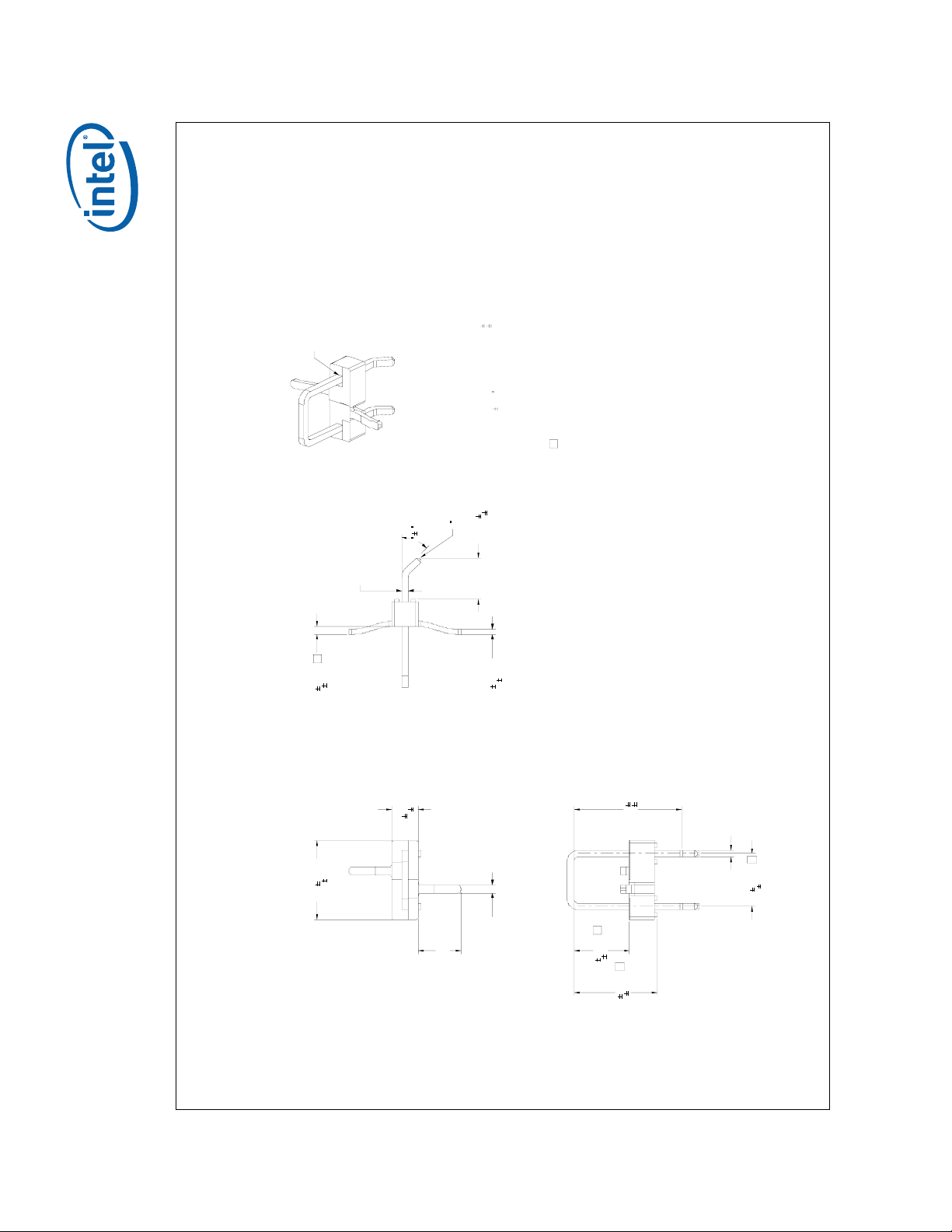
DATECHECKED BY
08/12/05KGTAN
DATEDRAWN BY
08/08/05KGTAN
DATEDESIGNED BY
- A INITIAL RELEASE 09/06/05 -
WIRE CLIP, MCH, BW, BTXD29081-001TOP
6. REMOVE ALL SHARP EDGES AND BURRS.
7. ALL DIMENSIONS SHOWN SHALL BE MEASURED FOR FAI
8. ALL SECONDARY UNIT DIMENSIONS ARE FOR REFERENCE ONLY.
THIRD ANGLE PROJECTION
UNLESS OTHERWISE SPECIFIED
DIMENSIONS ARE IN MILLIMETERS
ITEM NO
IN ACCORDANCE WITH ASME Y14.5M-1994
INTERPRET DIMENSIONS AND TOLERANCES
QTY
.189[]
4 4.8
.071[]
4X R 1.8
NOTES: 1. THIS DRAWING TO BE USED IN CORRELATION WITH SUPPLIED 3D
DATABASE FILE. ALL DIMENSIONS AND TOLERANCES ON THIS
DRAWING TAKE PRECEDENCE OVER SUPPLIED FILE AND ARE
APPLICABLE AT PART FREE, UNCONSTRAINED STATE UNLESS
INDICATED OTHERWISE.
2. TOLERANCES ON DIMENSIONED AND UNDIMENSIONED
4 CRITICAL TO FUNCTION DIMENSION
FEATURES UNLESS OTHERWISE SPECIFIED:
DIMENSIONS ARE IN MILLIMETERS.
TOLERANCES: LINEAR 0.25
ANGLES: 3
3. MATERIAL:
TYPE: ASTM A228 MUSIC WIRE 1.8 0.1MM 4
PLATING: ELECTRO-LESS NICKEL OR EQUIVALENT UPON
INTEL APPROVAL.
5. MARK WITH INTEL P/N AND REVISION PER INTEL MARKING
STANDARD 164997; PER SEC 3.8 (POLYETHYLENE BAG)
A
1
OF
1
SHEET
DO NOT SCALE DRAWING
4:1
SIZE DRAWING NUMBER REV
A1 D29081 A
SCALE:
SEE NOTESSEE NOTES
FINISHMATERIAL
09/06/05DANA GRINDLE
DATEAPPROVED BY
Thermal and Mechanical Design Guide
8 7 6 5 4 3 2
.8[]
21.3
1.075[]
27.3
1.625[]
41.3
.019[]
0.5
2.465
62.6
.315[]
8
THIS DRAWING CONTAINS INTEL CORPORATION CONFIDENTIAL INFORMATION. IT IS DISCLOSED IN CONFIDENCE AND ITS CONTENTS
MAY NOT BE DISCLOSED, REPRODUCED, DISPLAYED OR MODIFIED, WITHOUT THE PRIOR WRITTEN CONSENT OF INTEL CORPORATION.
H
G
F
Figure 24. (G)MCH Chipsets Reference Heatsink for Balanced Technology Extended (BTX) Platforms – Clip
10.0
WITHIN
WIRE TERMINATION
.161[]
2X 4.1
.283[]
2X 7.2
C
4 132.6 3
2X 90
E
D
.051[]
2X R 1.3
2X 90
A
66.3
.930[]
2X 4 23.63
B
8 7 6 5 4 3 2 1
A
44
 Loading...