

Page 1

Intel® 41110 Serial to Parallel PCI Bridge
Design Guide
March 2006
Order Number: 310335-001
Page 2

INFORMATION IN THIS DOCUMENT IS PROVIDED IN CONNECTION WITH INTEL® PRODUCTS. NO LICENSE, EXPRESS OR IMPLIED, BY
ESTOPPEL OR OTHERWISE, TO ANY INTELLECTUAL PROPERTY RIGHTS IS GRANTED BY THIS DOCUMENT. EXCEPT AS PROVIDED IN
INTEL'S TERMS AND CONDITIONS OF SALE FOR SUCH PRODUCTS, INTEL ASSUM ES NO LIABILITY WHATSOEVER, AND INTEL DISCLAIMS
ANY EXPRESS OR IMPLIED WARRANTY, RELATING TO SALE AND/OR USE OF INTEL PRODUCTS INCLUDING LIABILITY OR WARRANTIES
RELATING T O FITNESS FOR A PARTICULAR PURPOSE, MERCHANTABILITY, OR INFRINGEMENT OF ANY PATENT, COPYRI GHT OR OTHER
INTELLECTUAL PROPERTY RIGHT. Intel products are not intended for use in medical, life saving, life sustaining applications.
Contact your local Intel sales office or your distributor to obtain the latest specifications and before placing your product order.
Copies of documents which have an ordering number and are referenced in this document, or other Intel literature may be obtained by calling
1-800-548-4725 or by visiting Intel's website at http://www.intel.com.
Intel is a trademark or registered trademark of Intel Corporation or its subsidiaries in the United States and other countries.
*Other names and brands may be cla imed as the property of others.
Copyright © Intel Corporation, 2006
ii Intel® 41110 Serial to Parallel PCI Bridge Design Guide
Page 3

Contents
Contents
1 About This Document ...................................................................................................................7
1.1 Terminology and Definitions .................................................................................................7
2 Introduction....................................................................................................................................9
2.1 PCI Express Interface Features............................................................................................9
2.2 PCI-X Interface Features......................................................................................................9
2.3 Power Management............................................................................................................10
2.4 SMBus Interface .................................................................................................................10
2.5 JTAG...................................................................................................................................12
2.6 Related Documents ............................................................................................................12
2.7 Intel® 41110 Serial to Parallel PCI Bridge Applications .....................................................13
3 Package Information ...................................................................................................................15
3.1 Package Specification ........................................................................................................15
4 Power Plane Layout ....................................................................................................................17
4.1 41110 Decoupling Guidelines......................... ...... ...... ....... ...... ....... ...... ....... .......................1 7
4.2 Split Voltage Planes............................................................................................................19
5 41110 Reset and Power Timing Considerations.......................................................................21
5.1 A_RST# and PERST# Timing Requirements.....................................................................21
5.2 VCC15 and VCC33 Voltage Requirements........................................................................21
6 General Routing Guidelines .......................................................................................................23
6.1 General Routing Guidelines................................................................................................23
6.2 Crosstalk.............................................................................................................................23
6.3 EMI Considerations ............................................................................................................24
6.4 Power Distribution and Decoupling.....................................................................................25
6.5 Trace Impedance................................................................................................................25
7 Board Layout Guidelines............................................................................................................27
7.1 Adapter Card Topology.. ....... ...... ....... ...... ....... ...... ...... ....... ...... ....... ....................................27
8 PCI-X Layout Guidelines.............................................................................................................29
8.1 Interrupts.............................................................................................................................29
8.2 PCI Arbitration ....................................................................................................................30
8.3 PCI General Layout Guidelines ..........................................................................................31
8.4 PCI Clock Layout Guidelines ..............................................................................................32
8.5 PCI-X Topology Layout Guidelines.....................................................................................35
8.6 41110 Layout Analysis............................. ....... ...... ...... ....... ....................................... ...... ....35
9 PCI Express Layout.....................................................................................................................41
9.1 General recommendations .................................................................................................41
9.2 PCI-Express Layout Guidelines..........................................................................................42
9.3 Adapter Card Layout Guidelines.........................................................................................42
10 Circuit Implementations..............................................................................................................45
10.1 41110 Analog Voltage Filters.......................... ...... ...... ....................................... ....... ...... ....45
Intel® 41110 Serial to Parallel PCI Bridge Design Guide iii
Page 4

Contents
10.2 41110 Reference and Compensation Pins.........................................................................48
11 41110 Customer Reference Boards...........................................................................................51
11.1 Board Stack-up..................................... ...................................... ....... ...... ....... ...... ....... .......51
11.2 Material...............................................................................................................................52
11.3 Impedance..........................................................................................................................52
11.4 Board Outline.................... ....... ...... ....... ...... ....... ...... ...... ....... ...... ....... .................................53
12 Design Guide Checklist ..............................................................................................................55
Figures
1 Microcontroller Block Diagram....................................................................................................11
2 41110 Microcontroller Connections............................................................................................12
3 41110 Block Diagram .................................................................................................................13
4 41110 Adapter Card Block Diagram...........................................................................................14
5 41110 Bridge Package Dimensions (Top View) .........................................................................15
6 41110 Bridge Package Dimensions (Side View)........................................................................16
7 Decoupling Placement for Core and PCI Express Voltage Planes ............................................17
8 Decoupling Placement for PCI/PCI-X 1.5V and 3.3V Voltage Planes........................................18
9 41110 Bridge Single-Layer Split Voltage Plane..........................................................................20
10 Crosstalk Effects on Trace Distance and Height........................................................................24
11 PCB Ground Layout Around Connectors ...................................................................................24
12 Cross Section of Differential Trace.............................................................................................26
13 Two-by-two Differential Impedance Matrix .................................................................................26
14 Adapter Card Stackup .............. ....... ...... ....... ...... ....... ...... ...... ....... ...... ....... ...... ...........................28
15 PCI RCOMP ...............................................................................................................................31
16 PCI Clock Distribution and Matching Requirements...................................................................33
17 Embedded PCI-X 133 MHz Topology ........................................................................................36
18 Embedded PCI-X 100 MHz Topology ........................................................................................37
19 PCI-X 66 MHz Embedded Routing Topology.............................................................................38
20 PCI 66 MHz Embedded Topology..............................................................................................39
21 PCI 33 MHz Embedded Mode Routing Topology.......................................................................40
22 PCI Analog Voltage Filter Circuit................................................................................................46
23 PCI Express Analog Voltage Filter Circuit..................................................................................47
24 Bandgap Analog Voltage Filter Circuit........................................................................................48
25 Reference and Compensation Circuit Implementations .............................................................49
26 Mechanical Outline of the 41110................................................................................................53
Tables
1 Terminology and Definitions .........................................................................................................7
2 41110 Decoupling Guidelines.....................................................................................................19
3 Adapter Card Stack Up, Microstrip and Stripline ........................................................................27
4 INTx Routing Table.....................................................................................................................29
5 Interrupt Binding for Devices Behind a Bridge...........................................................................30
6 PCI-X Signals .............................................................................................................................32
7 PCI/PCI-X Frequency/Mode Straps............................................................................................32
8 PCI-X Clock Layout Requirements Summary ............................................................................34
9 PCI-X Slot Guidelines.................................................................................................................35
iv Intel® 41110 Serial to Parallel PCI Bridge Design Guide
Page 5

Contents
10 Embedded PCI-X 133 MHz Routing Recommendations............................................................36
11 Embedded PCI-X 100 MHz Routing Recommendations............................................................37
12 PCI-X 66 MHz Embedded Routing Recommendations..............................................................38
13 PCI 66 MHz Embedded Table....................................................................................................39
14 PCI 33 MHz Embedded Routing Recommendations..................................................................40
15 Adapter Card Routing Recommendations..................................................................................42
16 Recommended R, L and C Values for 41110 Analog Filter Circuits...........................................45
17 SMBUs Address Configuration...................................................................................................49
18 CRB Board Stackup....................................................................................................................51
19 PCI Express Interface Signals....................................................................................................55
20 PCI/PCI-X Interface Signals .......................................................................................................56
21 Miscellaneous Signals ................................................................................................................57
22 SMBus Interface Signals ............................................................................................................58
23 Reset Pins ..................................................................................................................................59
24 Power and Ground Signals.........................................................................................................60
25 JTAG Signals......................... ....... ...... ....... ...... ....................................... ...... ....... ...... .................61
Intel® 41110 Serial to Parallel PCI Bridge Design Guide v
Page 6

Contents
Revision History
Date Revision Description
March 2006 001 Initial release.
vi Intel® 41110 Serial to Parallel PCI Bridge Design Guide
Page 7
About This Document 1
This document provides layout i nformation and guide lines for designing p latform or add-in board
applications with the Intel® 41110 Serial to Parallel PCI Bridge (also called the 411 10 Bridge). It is
recommended that this document be used as a guideline. Intel recommends employing best-known
design practices with board level simulation, signal integrity testing and validation for a robust
design.
Designers should note that this guide focuses upon specific design considerations for the 41110
Bridge and is not intended to be an all-inclusive list of all good design practices. Use this guide as
a starting point and use empirical data to optimize your particular design.
1.1 Terminology and Definitions
Table 1 provides a list of terms and definitions that may be useful when working with the 41110
Bridge product.
Table 1. Terminology and Definitions (Sheet 1 of 2)
Term Definition
Stripline in a PCB is composed of the
conductor inserted in a dielectric with GND
planes to the top and bottom.
Stripline
NOTE: An easy way to distinguish stripline
from microstrip is that you need to
strip away layers of the board to view
the trace on stripline.
Microstrip
Prepreg
Core
Intel® 41110 Serial to Parallel PCI Bridge Design Guide 7
Material used for the lamination process of manufacturing PCBs. It consists of a layer of
epoxy material that is placed between two cores. This layer melts into epoxy when heated and
forms around adjacent traces.
Material used for the lamination process of manufacturing PCBs. This material is two sided
laminate with copper on each side. The core is an internal layer that is etched.
Microstrip in a PCB is composed of the
conductor on the top layer above the dielectric
with a ground plane below
Page 8
About This Document
Table 1. Terminology and Definitions (Sheet 2 of 2)
Term Definition
Layer 1: copper
Prepreg
Layer 2: GND
Core
PCB
Example of a Four-Layer Stack
SSTL_2 Series Stub Terminated Logic for 2.5 V
JEDEC Provides standards for the semiconductor industry.
A network that transmits a coupled signal to another network is aggressor network.
Aggressor
Victim A network that receives a coupled cross-talk signal from another network is a victim network.
Network The trace of a PCB that completes an electrical connection between two or more components.
Stub Branch from a trunk terminating at the pad of an agent.
CRB Customer Reference Board
Downstream
Upstream
Local memory
DWORD 32-bit data word.
Flip Chip
Mode
Conversion
PCI-E PCI-Express
Downstream refers either to the relative position of an interconnect/system element (Link/
device) as something that is farther from the Root Complex, or to a direction of information
flow, i.e., when information is flowing away from the Root Complex.
Memory subsystem on the Intel XScale
busses.
FC-BGA (flip chip-ball grid array) chip packages are designed with processor core flipped up
on the back of the chip, facing away from the PCB. This allows more efficient cooling of the
package.
Mode Conversions are due to imperfections on the interconnect which transform differential
mode voltage to common mode voltage and common mode voltage to differential voltage.
Zo
Layer 3: VCC15
Prepreg
Layer 4: copper
Zo
Victim Network
Aggressor Network
Printed circuit board.
Example manufacturing process consists of
the following steps:
• Consists of alternating layers of core and
prepreg stacked
• The finished PCB is heated and cured.
• The via holes are drilled
• Plating covers holes and outer surfaces
• Etching removes unwanted copper
• Board is ti nned, coated with solder mask
and silk screened
Zo
Zo
®
processor DDR SDRAM or Peripheral Bus Interface
8 Intel® 41110 Serial to Parallel PCI Bridge Design Guide
Page 9

Introduction 2
The Intel® 411 1 0 Serial to Parallel PCI Bridge integrates a PCI Express-to-PCI bridge. The bridge
follows the PCI-to-PCI Bridge programming model. The PCI Express port is compliant to the PCI
Express Specification, Revision1.0. The PCI bus interface is fully compliant to the PCI Lo cal Bus
Specification, Revision 2.3.
2.1 PCI Express Interface Features
• PCI Express Specification, Revision 1.0b compliant.
• Support for single x8, single x4 or single x1 PCI Express operation.
• 64-bit addressing support.
• 32-bit CRC (cyclic redundancy checking) covering all transmitted data packets.
• 16-bit CRC on all link message information.
• Raw bit-rate on the data pins of 2.5 Gbit/s, resulting in a raw bandwidth per pin of 250 MB/s.
• Maximum realized bandwidth on PCI Express interface is 2 GB/s (in x8 mode) in each
direction simultaneously, for an aggregate of 4 GB/s.
2.2 PCI-X Interface Features
• PCI Local Bus Specification, Revision 2.3 compliant.
• PCI-to-PCI Bridge Specification, Revision 1.1 compliant.
• PCI-X Addendum to the PCI Local Bus Specification, Revision 1.0a compliant.
• 64-bit 66 MHz, 3.3 V, NOT 5 V tolerant.
• On Die Termi nati on (ODT) with 8.2KΩ pull-up to 3.3V for PCI signals.
• Six external REQ/GNT Pairs for internal arbiter on the PCIX bus segment respectively.
• Programmable bus parking on either the last agent or always on Int el® 41 1 10 S erial to Parallel
PCI Bridge.
• 2-level programmable round-robin internal arbiter with Multi-Transaction Timer (MTT)
• External PCI clock-feed support for asynchronous primary and secondary domain operation.
• 64-bit addressing for upstream and downstream transactions
• Downstream LOCK# support.
• No upstream LOCK# support.
• PCI fast Back-to-Back capable as target.
• Up to four active and four pending upstream memory read transactions
Intel® 41110 Serial to Parallel PCI Bridge Design Guide 9
Page 10

Introduction
• Up to two downstream delayed (memory read, I/O read/write and configuration read/write)
transaction.
• Tunable inbound read prefetch algorithm for PCI MRM/MRL commands
• Local initialization via SMBus
• Secondary side initialization via Type 0 configuration cycles.
2.3 Power Management
• Support for PCI Express Active State Power Management (ASPM) L0s link state
• Support for PCI PM 1.1 compatible D0, D3hot and D3cold device power states
• Support for PME# event propagation on behalf of PCI devices
2.4 SMBus Interface
• Compatible with System Management Bus Specification, Revision 2.0
• Slave mode operation only.
• Full read/write access to all configuration registers
2.4.1 SMBus for configuration register initialization
• Support for local initialization of the configuration registers can be implemented using a
microcontroller via SMB. Figure 1shows this SMBus and the data transfer that occurs between
the 41110 and the microcontroller.
• Configuration Register information is stored internally in a microcontroller and the
information is transferred to the product via System Managed Bus (SMBus) protocols when
the device receives power or reset.
• The requirements of the microcontroller are as follows:
— Supports I
— Has at least 256 Byte of internal EEprom space
— To facilitate this programming on the Customer Reference Board a Microchip part
PIC16F876A was used.
— Code space: estimated code size is ~2K words of program s pace and 32 words of RAM
2
C and SMBus Prot ocols
10 Intel® 41110 Serial to Parallel PCI Bridge Design Guide
Page 11
Figure 1. Micro c ontro l ler Block Diag ra m
Introduction
Se rial to P ar a lle l
PCI Bridge
2.4.2 Microcontroller Connections to the 41110
Figure 2 shows the SMB interface from the 41110 to the microcontroller.
Intel® 41110 Serial to Parallel PCI Bridge Design Guide 11
Page 12
Introduction
Figure 2. 41110 Microcontroller Connections
Serial to
Parallel PCI
Bridge
2.5 JTAG
• Compliant with IEEE Standard Test Access Port and Boundary Scan Architecture 1149.1a
2.6 Related Documents
• .
• PCI Express Specification, Revision 1.0, from www.pci-s ig.com.
• PCI Express Design Guide, Revision 0.5
• PCI Local Bus Specification, Revision 2.3, from www.pci-sig.com.
• PCI-X Addendum to the PCI Local Bus Specification, Revision 1.0a, from www.pci-sig.com.
• IEEE Standard Test Access Port and Boundary Scan Architecture 1149.1a
• System Management Bus Specification, Revision 2.0
12 Intel® 41110 Serial to Parallel PCI Bridge Design Guide
Page 13
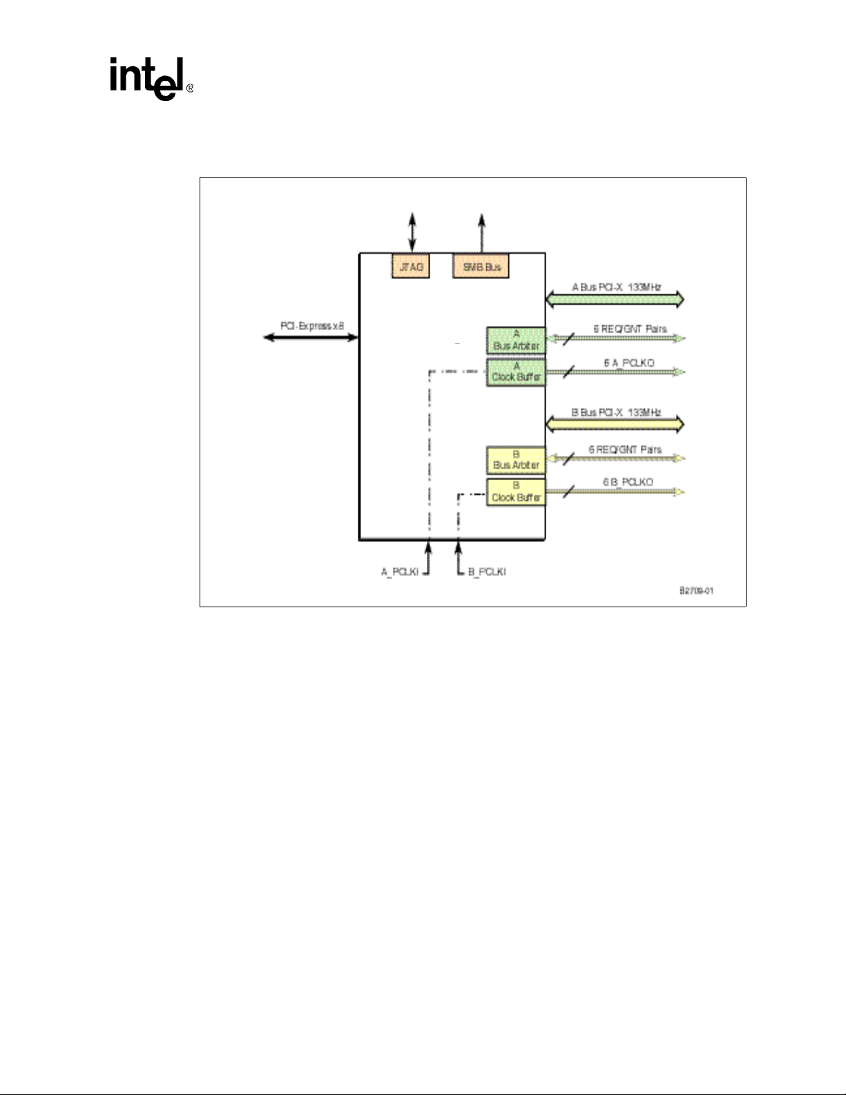
Figure 3. 41110 Block Diagram
Introduction
Serial to Parallel
PCI Bridge
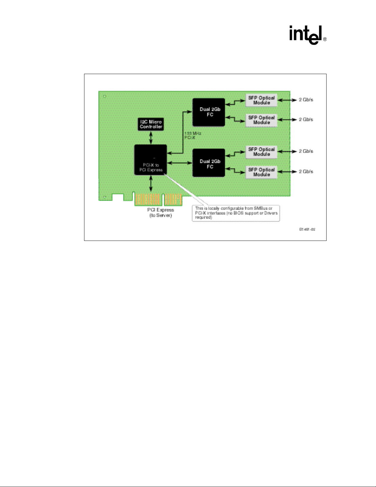
2.7 Intel® 41110 Serial to Parallel PCI Bridge Applications
This section provides a block diagram for a typical the 41110 application. This application shows a
PCI-E adapter card with two Dual 2Gb Fibre Channel controllers. Each of the PCI-X bus segmen ts
is connected to the Dual 2Gb Fibre Channel chip running at 133MHz. The two Dual FC chips
provides the four 2Gb/s outputs.
Intel® 41110 Serial to Parallel PCI Bridge Design Guide 13
Page 14
Introduction
Figure 4. 41110 Adapter Card Block Diagram
Serial to Pa rallel
PCI Bridge
14 Intel® 41110 Serial to Parallel PCI Bridge Design Guide
Page 15
Package Information 3
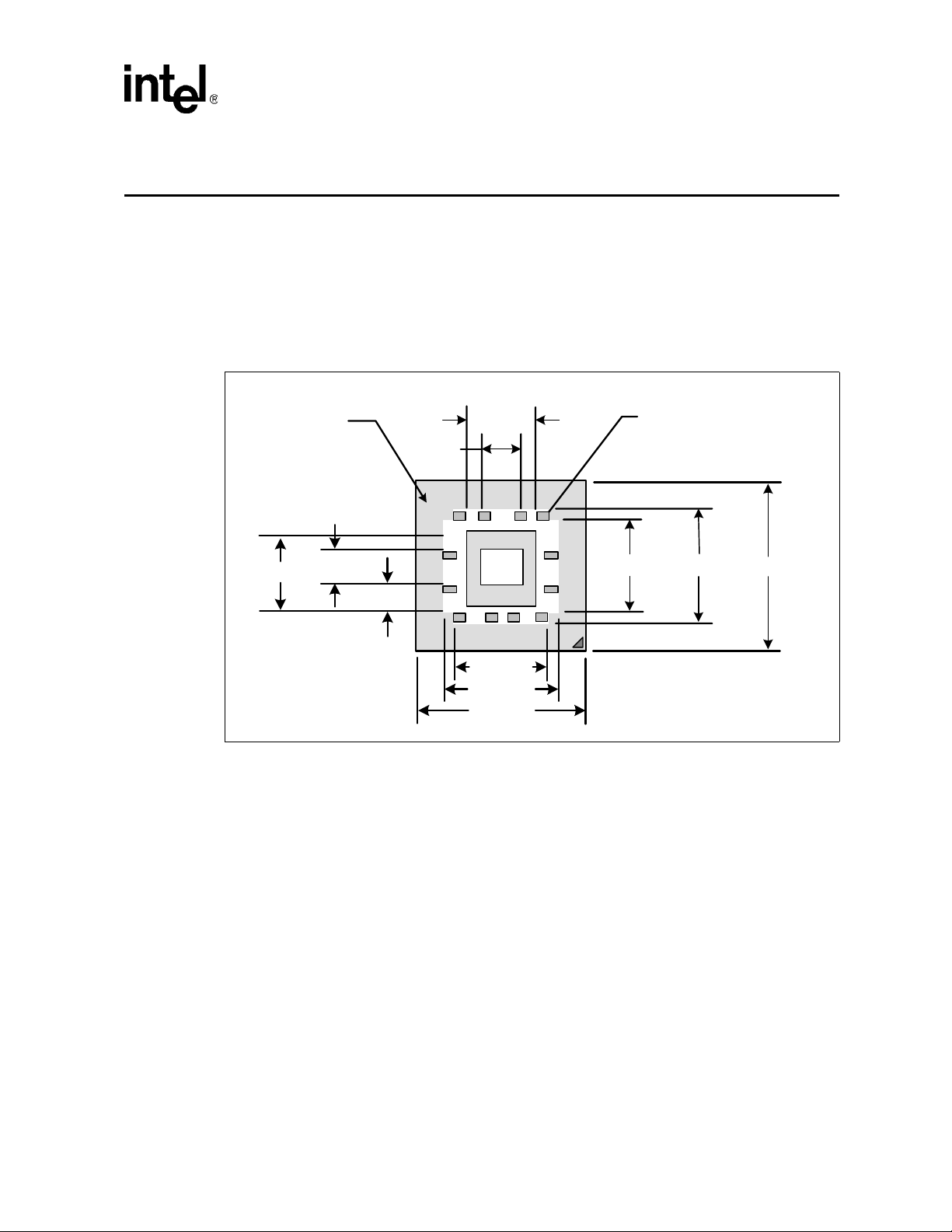
3.1 Package Specification
The 41110 Bridge is in a 567-ball FCBGA package, 31mm X 31mm in size, with a 1.27mm ball
pitch (see Figure 5 and Figure 6).
Figure 5. 41110 Bridge Package Dimensions (T o p View)
Handling
Exclusion
0. 547 in.
Area
0. 247 in.
0. 200 in.
0. 291 in.
0. 491 in.
17. 00 mm
21. 00 mm
31. 00 mm
Die
Keepout
Area
17. 00 mm 21 . 00 mm 31 . 00 mm
Intel® 41110 Serial to Parallel PCI Bridge Design Guide 15
Page 16
Package Information
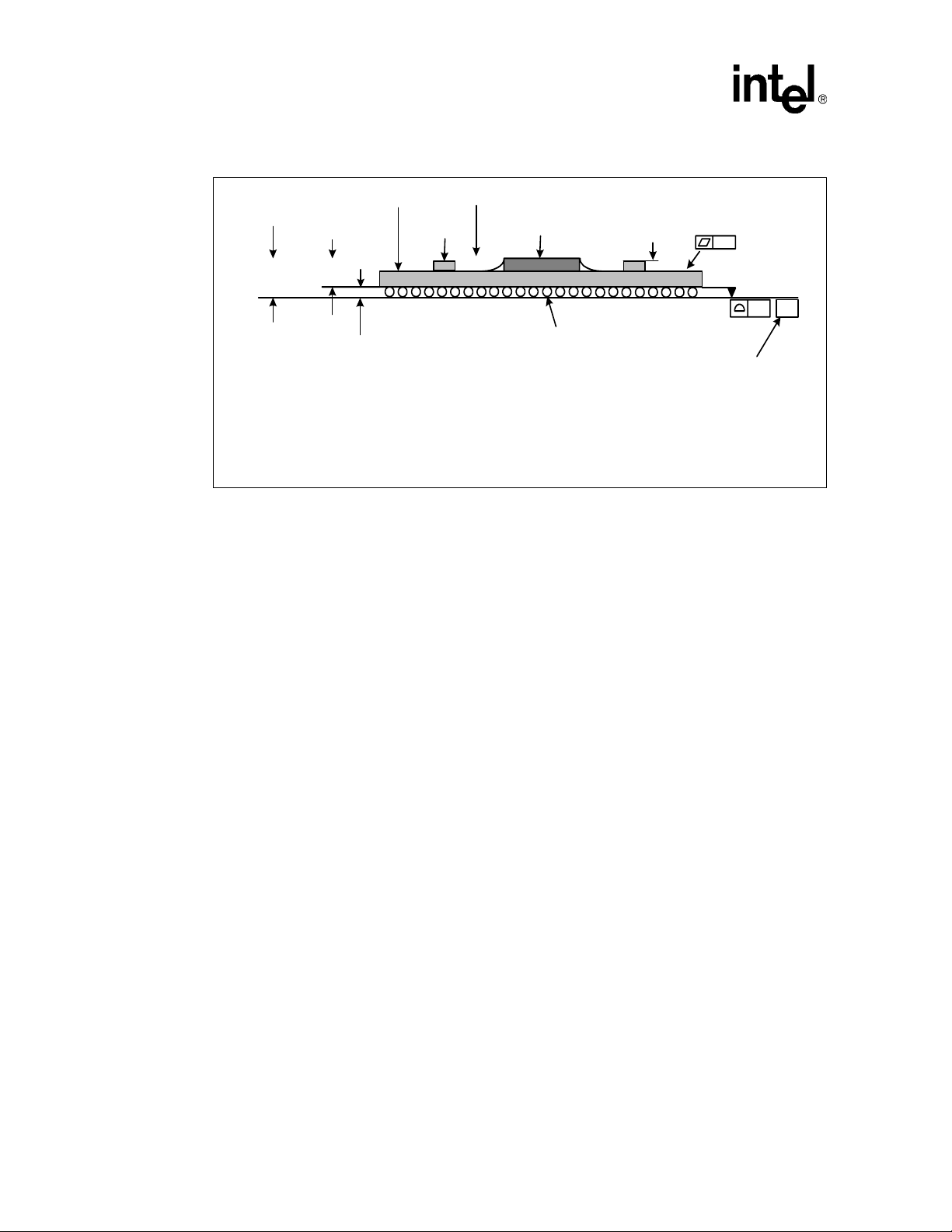
Figure 6. 41110 Bridge Package Dimensions (Side View)
Substrate
2.445±0.102 mm
2.010±0.099 mm
0.435±0.025 mm
Se e Note 3
Notes:
1. Primary datum -C- and seating plan are defined by the spherical crowns of the solder balls (shown before motherboard attach).
2. All dimensions and tolerances conform to ANSI Y14.5M-1994
3. BGA has a pre-SMT height of 0.5 mm and post-SMT height of 0.41-0.46 mm
4. Shown before motherboard attach; FCBGA has a convex (dom e shape) orientation before reflow and is expected to have a slightly
concave (bowl shaped) orientation after reflow.
0.84±0.05 mm
Decoup
Cap
Die
Seating Plane
0.7 mm Max
0.20
See Note 4.
0.20
Se e Note 1
Note: Primary datum -C- and seating plane are defined by the spherical crowns of the solder balls.
Note: All dimensions and tolerance s conform t o ANSI Y14.5M -1982
-C-
16 Intel® 41110 Serial to Parallel PCI Bridge Design Guide
Page 17
Power Plane Layout 4
This chapter provides details on the decoupling and voltage planes needed to bias the 41110
package.
4.1 41110 Decoupling Guidelines
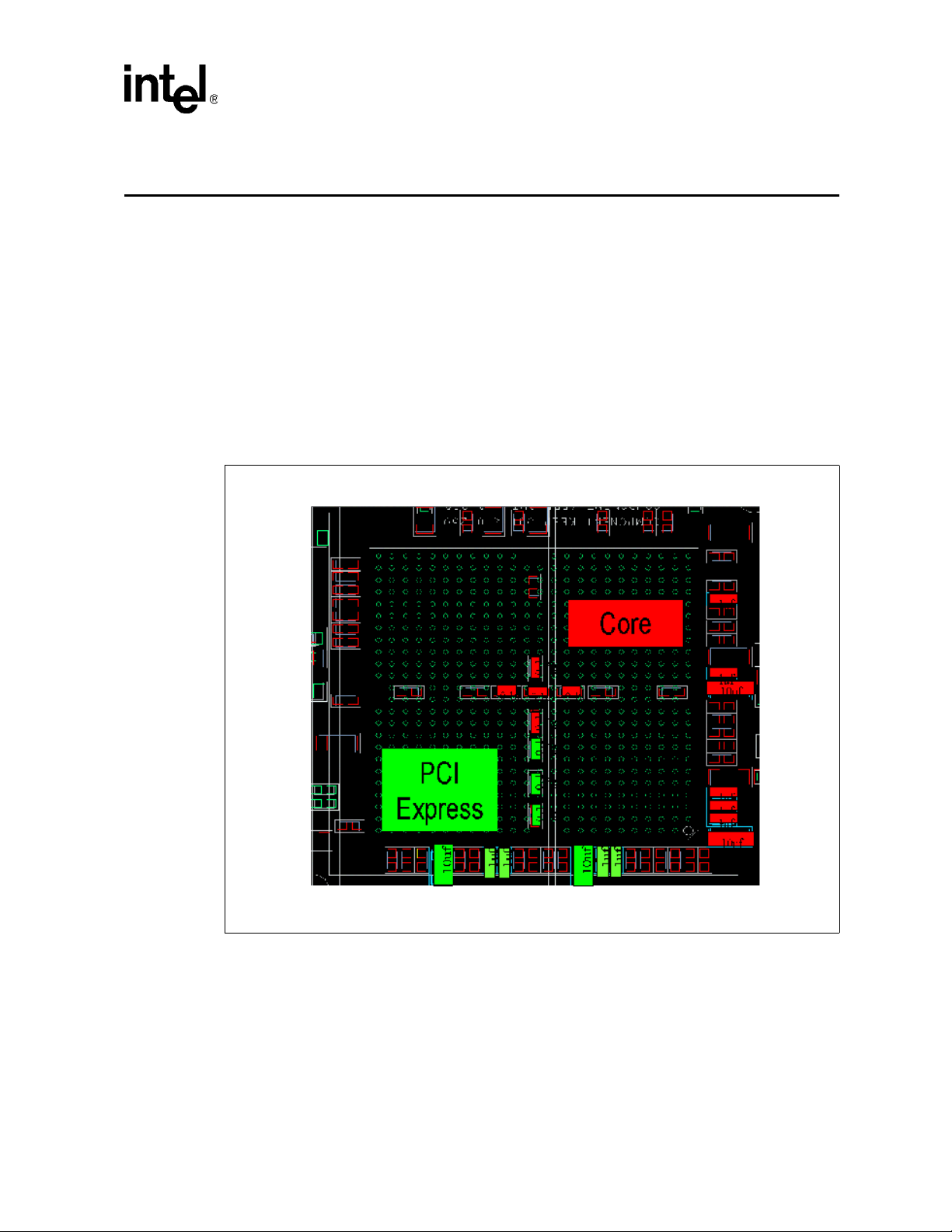
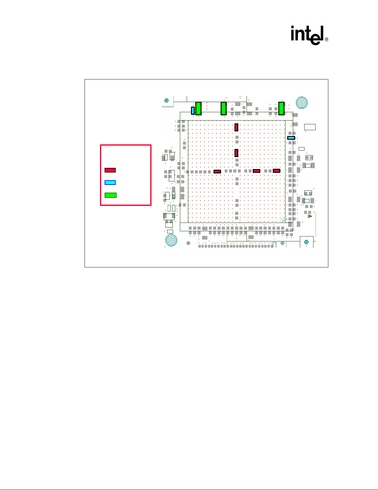
Table 2 lists the decoupling guidelines for the 41110. Figure 7 and Figure 8 provide the decoupling
capacitors around the 41110 ball grid pins.
Figure 7. Decoupling Placement for Core and PCI Express Voltage Planes
B2713-01
Intel® 41110 Serial to Parallel PCI Bridge Design Guide 17
Page 18
Power Plane Layout
Figure 8. Decoupling Placement for PCI/PCI-X 1.5V and 3.3V Volt age Planes
Capacitor Legend
0603-0.1 F
0603-1 F
1206-10 F
B2714-01
18 Intel® 41110 Serial to Parallel PCI Bridge Design Guide
Page 19
T a ble 2. 41110 Decoupling Guidelines
Power Plane Layout
Vol tage Plane Voltage
PCI/PCI-X
Voltage
PCI/PCI-X
Voltage
PCI/PCI-X
Voltage
Core Voltage 1.5V VCC15 0.1 0603 200 2.0 5
Core Voltage 1.5V VCC15 1.0 0805 200 2.3 5
Core Voltage 1.5V VCC15 10 1206 200 1.9 2
PCI Express
Voltage
PCI Express
Voltage
PCI Express
Voltage
3.3V VCC33 0.1 0603
3.3V VCC33 1.0 0603
3.3V VCC33 10 1206
1.5V VCCPE 0.1 0603 200 2.0 3
1.5V VCCPE 1 0805 200 2.3 4
1.5V VCCPE 10 1206 200 1.9 2
41110
Bridge
Pins
C
(uF)
Package
ESR
(mΩ)
50-
300
50-
300
50-
300
ESL
(nH)
1.0-
3.0
1.0-
3.0
1.0-
3.0
Caps
# of
5
As close as design
2
41110 Bridge BGA
As close as design
3
41110 Bridge BGA
As close as design
41110 BridgeBGA
As close as design
41110 Bridge BGA
As close as design
41110 Bridge BGA
As close as design
41110 Bridge BGA
Location
Beneath 41110
Bridge BGA
rules will allow to
rules will allow to
Beneath 41110
Bridge BGA
rules will allow to
rules will allow to
Beneath41110
Bridge BGA
rules will allow to
rules will allow to
4.2 Split Voltage Planes
There are two 1.5V voltage planes that supply power to the 4111 0:
• VCC15:1.5V ±5% (1.5V core voltage)
• VCCPE:1.5V ±3% (1.5V PCI Express voltage)
The 41110 Bridge core (VCC15), PCI-Express (VCCPE) voltages should be supplied by t wo
separate voltage regulators or a single regulator. If VCC15 and VCCPE is supplied by a single
voltage regulator the power planes should be split as shown in Figure 9.
Intel® 41110 Serial to Parallel PCI Bridge Design Guide 19
Page 20

Power Plane Layout
Note: Linear voltage regulators are recommended when using 1.5 Volt power supplies.
Figure 9. 41110 Bridge Single-Layer Split Voltage Plane
re
Core
PCI
Express
B2715-01
20 Intel® 41110 Serial to Parallel PCI Bridge Design Guide
Page 21

41110 Reset and Power Timing
Considerations 5
This chapter describes the 41110 reset timing considerations.
5.1 A_RST# and PERST# Timing Requirements
The PCI-X Specification requires that there is a 100ms delay from valid power (PERST#) to reset
deassertion (A_RST#). 41110 will keep A_RST# asserted for a minimum of 320ms after PERST#
is deasserted.
5.2 VCC15 and VCC33 Voltage Requirements
The following steps are the power sequencing requirements th at must be followed with the
41110:
1. The 41110 requires that the VCC33 voltage rail be no less than 0.5V below VCC15 (absolute
voltage value) at all times during 41110 operation, including during system power up and
power down. In other words, the f ollowing mu st always be t rue:
VCC33 >= (VCC15 – 0.5V)
This can be accomplished by placing a diode (with a voltage drop <0.5V) between VCC15 and
VCC33. A node will be connected to VCC15 and cathode will be connected to VCC33.
If VCC15 (1.5V PCI-X I/O voltage) and VCC15 (1.5V core voltage) are tied together on the
platform, then both voltages must meet the above rule.
Note: Linear voltage regulators are recommended when using 1.5 Volt power supplies.
2. If a voltage regulator solution is used which shunts VCC15 to ground while VCC33 is
powered, the maximum all owa ble t ime that VCC15 can be shunted to ground w hil e V C C33 is
fully powered is 20ms.
3. The maximum allowed time between VCC33 and VCC15 ramping is 525ms .
Note: There is no minimum sequencing time requirement other thanrequirements in Steps 2 and 3.
Intel® 41110 Serial to Parallel PCI Bridge Design Guide 21
Page 22

41110 Reset and Power Timing Considera tions
This page intentionally left blank.
22 Intel® 41110 Serial to Parallel PCI Bridge Design Guide
Page 23

General Routing Guidelines 6
This chapter provides some basic ro uting guidel ines for layout and design of a printed circuit board
using the 41110. The high-speed clocking required when designin g with the 41110 requires special
attention to signal integrity. In fact, it is highly recommended that the board design be simulated to
determine optimum layout for signal integrity. The information in this chapter provides guidelines
to aid the designer with board layout. Several factors influence the signal integrity of a 41110
design. These factors include:
• power distribution
• minimizing crosstalk
• decoupling
• layout considerations when routing the PCI Express bus and PCI-X bus interfaces
6.1 General Routing Guidelines
This section details general routing guidelines for designing with the 41110. The order in which
signals are routed varies from designer to designer. Some designers prefer to route all clock signals
first, while others pre fer to route al l high -speed b us sig nals fi rst. Ei ther ord er can be u sed, pr ovide d
the guidelines listed here are followed.
6.2 Crosstalk
Crosstalk is caused by capacitive and inductive coupling between signals. Crosstalk is composed of
both backward and forward cr osstalk comp onents. Back ward crosstalk cre ates an induced signal on
victim network that propagates in the opposite direction of the aggressor signal. Forward crosstalk
creates a signal that propagates in the same direction as the aggressor signal.
Circuit board analysis software is used to analyze your board layout for crosstalk problems.
Examples of 2D analysis tools include Parasitic Parameters from ANSOFT
*
Design
software is not available, the layout should be designed to maintain at least the minimum
recommended spacing for bus interfaces.
. Crosstalk problems occur when circuit etch lines run in parallel. When board analysis
• A general guideline to use is, that space distance between adjacent signals be a least 3.3 times
the distance from signal trace to the nearest return plane. The coupled noise between adjacent
traces decreases by the square of the distance between the adjacent traces.
• It is also recommended to specify the height of the above reference plane when laying out
traces and provide this parameter to the PCB manufacturer. By moving traces closer to the
nearest reference plane, the coupled noise decreases by the square of the distance to the
reference plane.
*
and XFS from Quad
Intel® 41110 Serial to Parallel PCI Bridge Design Guide 23
Page 24
General Routing Guidelines
Figure 10. Crosstalk Effects on Trace Distance and Height
P
H
aggressor victim
• Avoid slots in the ground plane. Slots increases mutual inductance thus increasing crosstalk.
• Make sure that ground plane surrounding connector pin fields are not completely cleared out.
When this area is completely cleared out, around the connector pins, all the return current must
flow together around the pin field increasing crosstalk. The preferred method of laying out a
connector in the GND layer is shown in Figure 11.
Figure 11. PCB Ground Layout Around Connectors
Connector
Connector Pins
Reference Plane
Reduce Crosstalk:
- Maximize P
- Minimize H
A9259-01
GND PCB Layer
A. Incorrect method B. Correct method
A9260-01
6.3 EMI Considerations
It is highl y recommen ded that good EMI design practice s be followed when designing with th e
41110.
• To minimize EMI on your PCB a useful technique is to not extend the power planes to the
edge of the board.
• Another technique is to surround the perimeter of your PC B layers with a GND trace. This
helps to shield the PCB with grounds minimizing radiation.
The below link can provide some useful general EMI guidelines considerations:
http://developer.intel.com/design/auto/mcs96/applnots/272673.htm
24 Intel® 41110 Serial to Parallel PCI Bridge Design Guide
Page 25

6.4 Power Distribution and Decoupling
Have ample decoupling to ground, for the power planes, to minimize the effects of the switching
currents. Three types of decoupling are: the bulk, the high-frequency ceramic, and the inter-plane
capacitors.
• Bulk capacitance consist of electrolytic or tantalum capacitors. These capacitors supply large
reservoirs of charge, bu t they are useful only at lower frequencies due to lead inductance
effects. The bulk capacitors can be located anywhere on the board.
• For fast switching currents, high-frequency low-inductance capacitors are most effective.
Place these capacitors as close to the device being decoupled as possible. This minimizes the
parasitic resistance and inductance associated with board traces and vias.
• Use an inter-plane capacitor between power and ground planes to reduce the effective plane
impedance at high frequencies. The general guideline for placing capacitors is to place highfrequency ceramic capacitors as close as possi ble to the module.
6.4.1 Decoupling
Inadequate high-frequency decoupling results in intermittent and unreliable behavior.
General Routing Guidelines
A general guideline recommends that you use the largest easily available capacitor in the lowest
inductance package. For specific decoupling requirements for a 41110 appli cation please refer to
Chapter 4.
6.5 Trace Impedance
All signal layers require contr olled impeda nce 60 Ω +/- 15%, microstrip or stripline for add-in card
applications. Selecting the appropriate board stack-up to minimi ze impedan ce variation s is very
important. When calculating flight times, it is important to consider the minimum and maximum
trace impedance based on the switching neighboring traces. Use wider s paces between traces, since
this can minimize trace-to-trace coupling, and reduce cros s talk.
When a different stack up is used the trace widths must be adjusted appropriately. When wider
traces are used, the trace spacing must be adjusted accordingly (linearly).
It is highly recommended that a 2D Field Solver be used to design the high-speed traces. The
following Impedance Calculator URL provide approximations for the trace impedance of various
topologies. They may be used to generate the starting point for a full 2D Field solver.
http://emclab.umr.edu/pcbtlc/
The following website link provides a useful basic guideline for calculating trace parameters:
http://www.ultracad.com/calc.htm
Intel® 41110 Serial to Parallel PCI Bridge Design Guide 25
Page 26

General Routing Guidelines
Note: Using stripline transmission lines may give better results than m icrost rip. This is due to th e
difficulty of precisely controlling the dielectric constant of the solder mask, and the difficulty in
limiting the plated thickness of microstrip conductors, which can substantially increase cross-talk.
6.5.1 Differential Impedance
The PCI Express standard defines a 100 Ω differential impedance. This sect ion provides some basi c
background information on the differential impedance calculations. In the cross section of
Figure 12 shows the cross section of two traces of a differential pair.
Figure 12. Cross Section of Different ial Trace
Ground reference plane
B2716 -01
To calculate the coupled impedance requires a 2x2 matrix. The diagonal values in the matrix
represent the impedance of the traces to ground and the off-diagonal values provide a measure of
how tightly the traces are coupled. The “differential impedance is the value of the line-to-line
resistor terminator that optimally terminates pure differential signals.” The two by two matrix is
shown below as:
Figure 13. Two-by-two Differential Impedance Matrix
Z11 Z12
=
Z
o
Z21 Z22
For a symmetric trace Z11 = Z22, the differential impedance can be calculated from this equation:
Z
differential
For two traces to be symmetric, they must have the same width, thickness and height above the
ground plane.
= 2(Z11-Z12)
1
With the traces terminated with the appropriate differential, impedance ringing is
minimized.
B2717 -01
1. “Terminating Differential Signals on PCBs”, Steve Kaufer and Kelee Crisafulli, Printed Circuit Design, March 1999
26 Intel® 41110 Serial to Parallel PCI Bridge Design Guide
Page 27

Board Layout Guidelines 7
This chapter provides details on adapter card stackup suggestions. It is highly recommend ed that
signal integrity simulations be run to verify each 41110 PCB layout especially if it deviates from
the recommendations listed in these design guidelines.
7.1 Adapter Card Topology
The 41110 will be implemented on PCI-E adapter cards with an eight layer stackup PCB. The
specified impedance range for all adapter card implementations will be 60
will be made for interfaces specified at other impedances. Table 3 defines the typical layer
geometries for eight layer boards.
T a ble 3. Adapter Card Stack Up, Microstrip and Stripline
Ω +/-15%. Adjustments
Variable Type
Solder Mask Thickness (mil) N/A 0.8 0.6 1.0
Solder Mask E
Core Thickness (mil) N/A 2.8 3.0 3.2
Core E
Plane Thickness (mil)
Trace Height
Trace Thickness (mil)
Trace Width (mil) Microstrip 4.0 2.5 5.5
Total Thickness (mil) FR4 62.0 56.0 68.0
(mil)
Preg E
N/A 3.65 3.65 3.65
r
N/A 4.3 3.75 4.85 2113 material
r
Power 2.7 2.5 2.9
Ground 1.35 1.15 1.55
13.53.33.7
23.53.33.7
3 10.5 9.9 11.1
Microstrip 4.30 3.75 4.85 2113 material
Stripline1 4.30 3.75 4.85 2113 material
r
Stripline2 4.3 3.75 4.85
Microstrip 1.75 1.2 2.3
Stripline 1.4 1.2 1.6
Stripline 4.0 2.5 5.5
Nominal
(mils)
Minimum
(mils)
Maximum
(mils)
Notes
The trace height will be determined to
achieve a nominal 60 Ω.
7628 material. Trace height 3 is composed
of one piece of 2113 and one piece of
7628.
Trace Spacing (using
microstrip E2E/C2C)
Trace Spacing (using
stripline E2E/C2C)
Trace Impedance
[12]/[16]
[12]/[16]
Microstrip 60 51 69
Stripline 60 51 69
Intel® 41110 Serial to Parallel PCI Bridge Design Guide 27
Page 28

Board Layout Guidelines
Note: Each interface will set the trace spacing based on its signal integrity of differential impedance
requirements. For the purposes of the building the transmission line models, it is assumed the
artwork is very accurate and therefore a constant. All the variability in the trace spacing is the result
of the tolerances of the trace width.
Figure 14. Adapter Card Stackup
L8
Stripline
Trace
Spacing
Microstrip
Trace
Width
L1
L3
Stripline
Trace
Width
Microstrip Trace Thickness
Solder Mask Thickness
Trace Height 1
Trace Height 2
Stripline Trace Thickness
Trace Height 3
Core Thickness
Plane Thickness
L4
B1436-01
Microstrip
Trace
Spacing
L1
L2 (GND)
L3
L4 (VCC)
Total Thicken ss
L5 (VCC)
L4
L7 (GND)
28 Intel® 41110 Serial to Parallel PCI Bridge Design Guide
Page 29

PCI-X Layout Guidelines 8
This chapter describes several factors to be considered with a 41110 PCI/PCI-X design. These
include the PCI IDSEL, PCI RCOMP, PCI Interrupts and PCI arbitration.
8.1 Interrupts
PCI Express provides interrupt messages that emulate the legacy wired mechanism. This allows IO
devices to signal PCI-style interrupts using a pair of ASSERT and DEASSERT messages This
message pairing preserves the level-sensitive semantics of the PCI interrupts on PCI Express.
The 41110 uses four interrupts - A_INTA:A_INTD on bus A segment corresponding to the four
interrupts defined in the PCI specification. The 41110 routes its PCI interrupt pins and the internal
interrupts to PCI Express INTx interrupts according to Table 4.
Table 4. INTx Routing Table
A_INT# Interrupt Pins PCI Express INTx Message
A_INTA INTA
A_INTB INTB
A_INTC INTC
A_INTD INTD
The 411 10 wi ll use its primary bu s number and dev ice number in the Requ ester ID field fo r the PCI
Express INTx messages. As stated in the PCI Express specification, the function number is
reserved for interrupt messages and wil l always be 0.
Intel® 41110 Serial to Parallel PCI Bridge Design Guide 29
Page 30

PCI-X Layout Guidelines
Note: PCI Express Assert_INTx/Deassert_INTx messages are not inhibited by the BME bit.
8.1.1 Interrupt Routing for Devices Behind a Bridge
Given the legacy interrupt sharing scheme shown in Table 5, to get the best legacy interrupt
performance (by reducing interrupt sharing), adapter boards have to select the appropriate
A_INTX# (where X is A, B, C or D) inpu t pin to us e on the P CI bus segm ent. The ch osen inte rrupt
input also imposes a PCI device number requirement for the interrupt source as specified in the
PCI-to-PCI Bridge specification and reproduced in Table 5
Table 5. Interrupt Binding for Devices Behind a Bridge
.
Device Number on
Secondary Bus
a
. 4, 8b, 12, 16, 20, 24, 28
-
b
1, 5, 9
, 13, 17, 21, 25, 29
b
2, 6, 10
3, 7, 11
a. Device number 0 is reserved for the Bridge and should not be assigned to secondary devices.
b. AD[27:24] which correspond to devices 11:8 should not be used for IDSEL# connections as these signals are used
, 14, 18, 22, 26, 30
b
, 15, 19, 23, 27, 31
when accessing the extended configuration space in the bridge from the secondary bus.
Interrupt Pin on Device Interrupt on 41110 Bridge
INTA# INTA#
INTB# INTB#
INTC# INTC#
INTD# INTD#
INTA# INTB#
INTB# INTC#
INTC# INTD#
INTD# INTA#
INTA# INTC#
INTB# INTD#
INTC# INTA#
INTD# INTB#
INTA# INTD#
INTB# INTA#
INTC# INTB#
INTD# INTC#
8.2 PCI Arbitration
The 41110 supports a high-performance internal PCI arbiter that supports up to seven masters on
each PCI segment A and B PCI Buses. The request inputs into the internal arbiter include: six
external request inputs and 1 internal request input. All request inputs to the internal arbiter are
split into two groups, a high priority group and a low priority group. Any master, including the
internal master, c an be p rog rammed to be i n eit her of the t wo g rou ps . Thi s could al so m ean that all
the request inputs into the arbiter could be in one single group. Within a group, priority is roundrobin. The entire low-priorit y group represents one slot in the high priority group. The 41110
provides a 16-bit arbiter control register to control two aspects of the internal arbiter behavior:
• Priority group for a master (i.e., whether a master is in low priority group or high priority
group).
30 Intel® 41110 Serial to Parallel PCI Bridge Design Guide
Page 31

• Bus parking on last PCI agent or the bridge.
By default, the arbiter parks the bus on the bridge and drives the A/D, C/BE# and PAR lines to a
known value while the bus is idle.
8.2.1 PCI Resistor Compensation
Figure 15 provides the recommended resistor compensation pin termination for the PCI A bus.
Figure 15. PCI RCOMP
RCOMP
100
PCI-X Layout Guidelines
Ω
– 1%
8.3 PCI General Layout Guidelines
For acceptable signal integrity with bus speeds up to 133MHz it is important to PCB design layout
to have controlled impedance.
• Signal traces should have an unloaded impedance of 60 +/- 10% Ω.
• Signal trace velocity should be roughly 150 – 190ps/inch
There are a couple of general guidelines which s hould be used when routing your PCI bus signals:
• Avoid routing signals > 8”.
• The following signals have no length restrictions: A_INTA#, A_INTB#, A_INTC#,
A_INTD#, and TCK, TDI, TDO, TMS and TRST#. Most PCI-X signals are timing critical.
These signals have length restrictions for propagation, setup, and hold requirements. Table 6
shows the PCI-X signals.
B2718 -01
Intel® 41110 Serial to Parallel PCI Bridge Design Guide 31
Page 32

PCI-X Layout Guidelines
Table 6. PCI-X Signals
A PCI Bus Segment:
Timing Critical Signals
Reset Signals
Non Timing Critica l
Signals
A_ACK64#, A_AD[63:0], A_C BE _ [7: 0] # , A_DEVSEL#, A_FRAME#,
A_GNT_[5:0]#, A_IRDY#, A_LOCK#, A_PAR64, A_REQ64#, A_REQ_[5:0]#,
A_STOP#, A_TRDY#, A_CLKO [6: 0 ], A_C LKI
A PCI Bus Segment:
A_RST#, A_PME#
A PCI Bus Segment:
A_133EN, A_IRQ[15:0]#, A_M 66EN, A_PCIXCAP, A_PERR#, A_SERR#
Table 7. PCI/PCI-X Frequency/Mode Straps
A_PCIXCAP A_M66EN A_133EN(on
00XPCI 33
01XPCI 66
PCI-X 66MHz cards connect this
signal to ground through a 10KΩ
±5% resistor in parallel with a
0.01uF ±10% capacitor.
PCI-X 133 MHz cards connect
PCIXCAP to ground through a
0.01uF ±10% capacitor.
PCI-X 133 MHz cards connect
PCIXCAP to ground through a
0.01uF ±10% capacitor.
XXPCI-X 66
X0PCI-X 100
X1PCI-X 133
board)
Note: All signals sampled on the rising edge of PERST#.
8.3.1 PCI Pullup Resistors Not Required
PCI control signal s on the 41110 do NOT require pullup resi stor s on the adapt er card to ens ure that
they contain stable values when no agent is actively driving the bus. These include:
A_ACK64#, A_AD[63:32], A_CBE#[7:4], A_DEVSEL#, A_FRAME#, A_INTA#, A_INTB#,
A_INTC#, A_INTD#, A_IRDY#, A_PERR#, A_PAR, A_GNT#[5:0], A_REQ#[5:0], A_LOCK#,
A_PAR64, A_REQ64#, A_SERR #, A_STOP#, and A_TRDY#
Bus
Mode/
Freq
8.4 PCI Clock Layout Guidelines
The PCI-X Addendum to the PCI Local Bus Specification, Revision 1.0a compliant, allows a
maximum of 0.5 ns clock skew timing for each of the PCI-X frequencies: 66 MHz, 100 MHz and
133 MHz. A typical PCI-X application may require separate clock point-to-point connections
32 Intel® 41110 Serial to Parallel PCI Bridge Design Guide
Page 33
distributed to each PCI device. The 411 10 provides seven bu f fered cl ocks o n th e PCI b us to conn ect
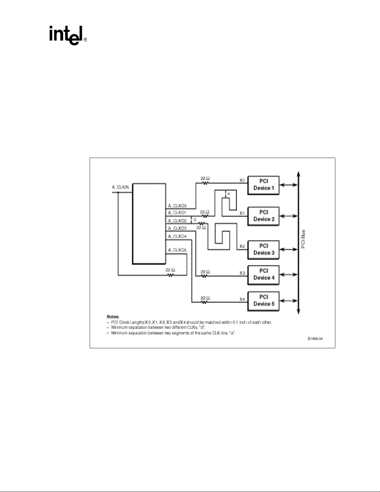
to multiple PCI-X devices. The Figure 16 shows the use of four PCI “A” clock outputs and length
matching requirements. . The recommended clock buffer layout are specified as follows:
• Match each of the used the 41 1 1 0 outpu t clock len gths A_CLK[6:0 ] to within 0.1”to h elp keep
the timing within the 0.5 ns maximum budget.
• Keep the distance between the clock lines and other signals “d” at least 25 mils from each other.
• Keep the distance between the clock line and itself “a” at a minimum of 25mils apart (for
serpentine clock layout).
• A_CLKIN gets connected to A_CLKO6 through a 22Ω +/- 1% resistor The 22 +/- 1% Ω
resistor is within 500 mils of A_CLKO.
Figure 16. PCI Clock Distribution and Matching Requirements
Serial to
Parallel PCI
Bridge
PCI-X Layout Guidelines
Intel® 41110 Serial to Parallel PCI Bridge Design Guide 33
Page 34

PCI-X Layout Guidelines
Table 8. PCI-X Clock Layout Requirements Summary
Parameter Routing Guidelines
Signal Group PCI Clocks A_CLK[6:0]
Reference Plane Route over unbroken ground or power plane
Stripline Tr ace Width 4 mils
Stripline Trace Spacing: Separation between two
different clock lines, “d” clock lines
Stripline Trace Spacing: Separation between two
segments of the same clock line (on serpentine
layout), “a” dimension
Stripline T race Sp acing: Separation between clocks
and other lines
Length Matching Requirements
Total Length of the 41110 PCI CLKs on the adapter
card
A_CLKIN Series Termination
A_CLK[6:0] Series Termination
Routing Guideline 1
Routing Guideline 2 Minimize number of vias
25 mils center to center from any other signal
25 mils center to center from any other signal
50 mils center to center from any other signal
All 41110 Output Clocks A_CLK[6:0] connected to
devices must be length matched to 0.1 inch of each
other.
The clock feedback line lengths from A_CLKOUT to
A_CLKIN should be length matched to all other clock
lines within 0.1”.
10” -14”
Connect A_CLKIN to one end of a 22Ω +/- 1% resistor
and the other end connected to A_CLKOUT
Each of the clock outputs A_CLKO[6:0] should have
series 22Ω resistor located within 500 mils of the
41110 clock output.
Point to point signal routing should be used to keep
the reflections low.
34 Intel® 41110 Serial to Parallel PCI Bridge Design Guide
Page 35
8.5 PCI-X Topology Layout Guidelines
The PCI-X Addendum to the PCI Local Bus Specification, Revision 1.0a compliant, recommends
the following guide lines f or th e number of loads for your PC I-X d esigns. Any deviati on fro m these
maximum values requires close attention to layout with regard to loading and trace lengths.
Table 9. PCI-X Slot Guidelines
Frequency Maximum Loads Maximum Number of Slots
66 MHz 8 4
100 MHz 4 2
133 MHz 2 1
8.6 41110 Layout Analysis
The following sections describes layout recommendations based on the signal integrity analysis.
This analysis was conducted using the following parameters:
• Card stack up: 60 Ω +/- 15% single-ended impedance
• Driver Model 41110 IBIS
• Receiver Model: generic models for PCI-X and PCI
PCI-X Layout Guidelines
• Driver Package Model: 41110 Model
• Cross talk and ISI impact on timing were not modeled
Intel® 41110 Serial to Parallel PCI Bridge Design Guide 35
Page 36
PCI-X Layout Guidelines
8.6.1 Embedded PCI-X 133 MHz
This section lists the routing recommendations for PCI-X 133 MHz without a slot. Figure 17 shows
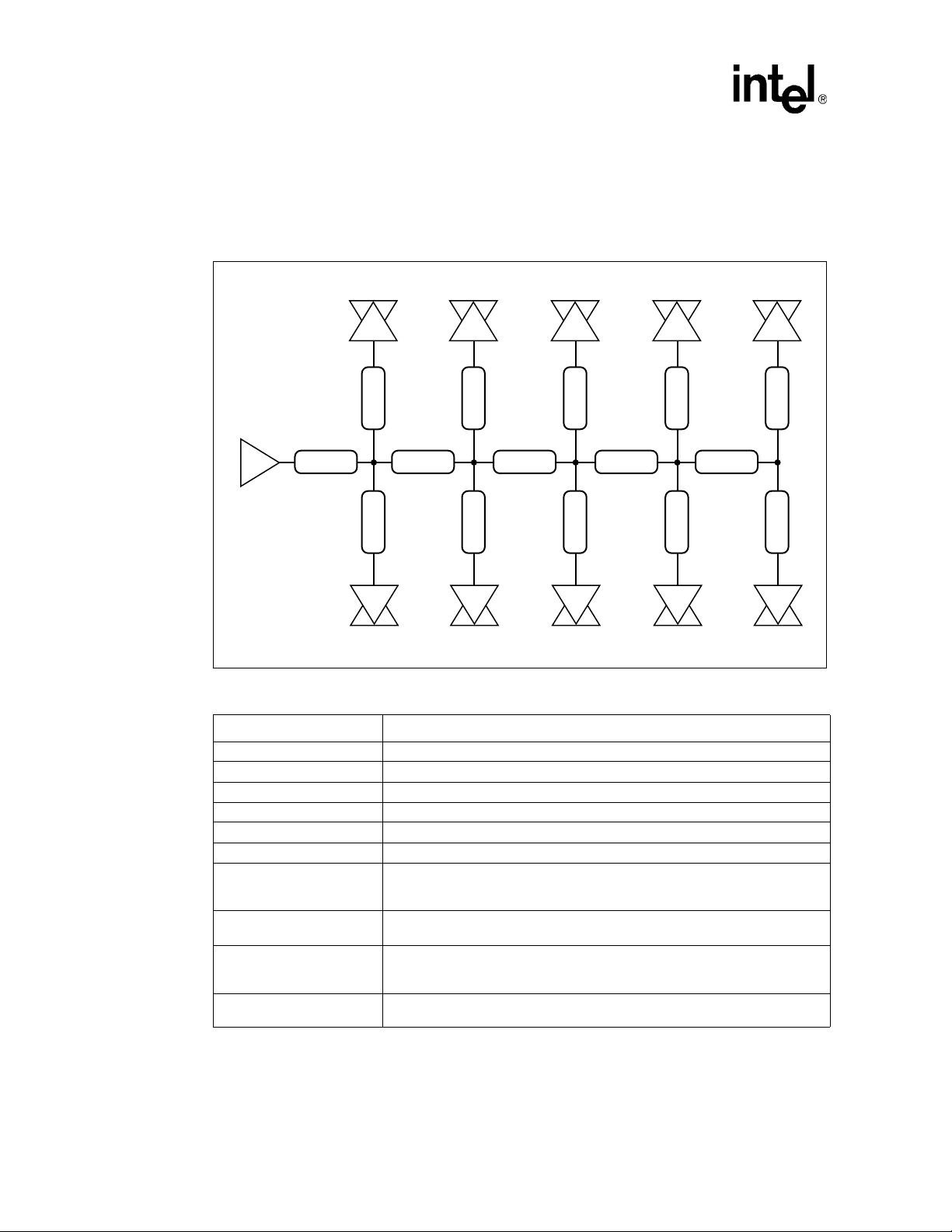
the block diagram of this topology and Table 10 describes the routing recommendations.
Figure 17. Embedded PCI-X 133 MHz Topology
TL1
EM1
TL_EM2 TL_EM1
EM2
Table 10. Embedded PCI-X 133 MHz Routing Recommendations
Parameter Routing Guideline for Lower AD Bus
Reference Plane Route over an unbroken ground plane
Board Impedance 60 Ω +/- 15%
Stripline Trace Spacing 12 mils from edge to edge
Microstrip Trace Spacing 18 mils, from edge to edge
Break Out 5 mils on 5 mils spacing. Maximum length of breakout region can be 500 mils
Group Spacing Spacing from other groups: 25 mils min, edge to edge
Trace Length 1 (TL1): From
41110 signa l Bal l to fi rs t
junction
Trace Length 3 junction of
TL_EM1 and TL_EM2 to the
embedded device
Length Matching
Requirements:
Number of vias 3 vias max per path
1.75” min - 4.0” max
1.25” min - 3.25” max
Clocks coming form the clock driver must be on the same layer and length
matched to within 25 mils.
B2719 -01
36 Intel® 41110 Serial to Parallel PCI Bridge Design Guide
Page 37
8.6.2 Embedded PCI-X 100 MHz
This section lists the embedded routing recommendations for PCI-X 100 MHz. Figure 18 shows
the block di agram of this topology and Table 11 describes the routing recommendations.
Figure 18. Embedded PCI-X 100 MHz Topology
PCI-X Layout Guidelines
TL_EM1
EM1
TL1
Table 11. Embedded PCI-X 100 MHz Routing Recommendations
Parameter Routing Guideline for Lower AD Bus
Reference Plane Route over an unbroken ground plane
Board Impedance 60 Ω +/- 15%
Stripline Trace Spacing 12 mils from edge to edge
Microstrip Trace Spacing 18 mils, from edge to edge
Break Out 5 mils on 5 mils spacing. Maximum length of breakout region can be 500 mils
Group Spacing Spacing from other groups: 25 mils min, edge to edge
Trace Length 1 (TL1): From
41110 signal Ball to first
junction
Trace Length: TL_EM1: from
41110 signal ball to the first
embedded device
Trace Length TL_EM2 TL_EM3: from junction to the
embedded device
Length Matching
Requirements:
Number of vias 4 vias max per path
0.5” min - 3.0” max
2.5” min - 3.5” max
1.5” min - 3.5” max
Clocks coming form the clock driver must be on the same layer and length
matched to within 25 mils.
TL_EM3
TL_EM2
EM3
EM2
B2720 -01
Intel® 41110 Serial to Parallel PCI Bridge Design Guide 37
Page 38

PCI-X Layout Guidelines
8.6.3 PCI-X 66 MHz Embedded Topology
Figure 19 and Table 12 provide routing details for a topology with an embedded PCI-X 66 MHz
application.
Figure 19. PCI-X 66 MHz Embedded Routing Topology
TL1
EM1
TL2
TL_EM2 TL_EM1
EM2
EM3
TL3
TL_EM4 TL_EM3
EM4
Table 12. PCI-X 66 MHz Embedded Routing Recommendations
Parameter Routing Guideline for Lower AD Bus
Reference Plane Route over an unbroken ground plane
Board Impedance 60 Ω +/- 15%
Stripline Trace Spacing 12 mils edge to edge
Microstrip Trace Spacing 18 mils, edge to edge
Break Out 5 mils on 5 mils. Maximum length of breakout region can be 500 mils
Group Spacing Spacing from other groups: 25 mils min, edge to edge
Trace Length 1 (TL1): From
41110 signa l Bal l to fi rs t
junction
Trace Length TL2 to TL4 between junctions
Trace Length TL_EM1 to
TL_EM8 from junction
connector to the embedded
device
Length Matching
Requirements:
Number of vias 4 vias max.
1.0” - 5.0” max
1.0” min - 2.5” max
2.0” min - 3.0” max
Clocks coming form the clock driver must be length matched to within 25 mils
and routed identical in layers.
EM5
TL_EM6 TL_EM5
EM6
EM7
TL4
TL_EM8 TL_EM7
EM8
B2721 -01
38 Intel® 41110 Serial to Parallel PCI Bridge Design Guide
Page 39

8.6.4 PCI 66 MHz Embedded Topology
Figure 20 and Table 13 provide routing details for a topology with an embedded PCI 66 MHz
design.
Figure 20. PCI 66 MHz Embedded Topology
PCI-X Layout Guidelines
Table 13. PCI 66 MHz Embedded Table
Parameter Routing Guideline for Lower AD Bus
Reference Plane Route over an unbroken ground plane
Board Impedance 60 Ω +/- 15%
Microstrip Trace Spacing 18 mils center to center
Stripline Trace Spacing 12 mils center to center
Group Spacing Spacing from other groups: 25 mils min, edge to edge
Breakout
Trace Length 1 TL1: From 41110 signal Ball to first
junction
Trace Length TL2 between junctions 0. 5” min - 3.5” max
Trace Length TL_EM1 to TL_EM4 from junction to
embedded devices
Length Matching Requirements
Number of vias 4 vias max.
P
TL1
EM1
TL2
TL_EM2 TL_EM1
EM2
5 mils on 5 mils spacing. Maximum length of breakout
region can be 500 mils.
5.0” max
2.0” min - 3.0” max
Clocks coming from the clock driver must be length
matched to within 25 mils.
EM3
TL_EM4 TL_EM3
EM4
B2722 -01
Intel® 41110 Serial to Parallel PCI Bridge Design Guide 39
Page 40
PCI-X Layout Guidelines
8.6.5 PCI 33 MHz Embedded Mode Topology
Figure 21 and Table 14 provide routing details for a topology with an embedded PCI 33 MHz
design.
Figure 21. PCI 33 MHz Embedded Mode Routing Topology
TL1
EM1
TL2
TL_EM2 TL_EM1
EM2
EM3
EM4
EM5
TL3
TL_EM4 TL_EM3
EM6
Table 14. PCI 33 MHz Embedded Routing Recommendations
Parameter Routing Guideline for Lower AD Bus
Reference Plane Route over an unbroken ground plane
Board Impedance 60 Ω +/- 15%
Stripline Trace Spacing 12 mils, edge to edge
Microstrip Trace Spacing 18 mils edge to edge
Group Spacing Spacing from other groups: 25 mils min, edge to edge
Breakout 5 mils on 5 mils spacing. Maximum length of breakout region can be 500 mils.
Trace Length 1 TL1: From
41110 signa l Bal l to fi rs t
junction
Trace Length TL2 to TL5 between junctions
Trace Length TL_EM1 to
TL_EM10 from junction to
embedded devices
Length Matching
Requirements
5.0” max
0.5” min - 3.5” max
2.0” min - 3.0” max
Clocks coming from the clock driver must be length matched to within 25 mils.
TL_EM6 TL_EM5
TL4
EM7
TL_EM8 TL_EM7
EM8
EM9
TL5
TL_EM10 TL_EM9
EM10
B2723 -01
40 Intel® 41110 Serial to Parallel PCI Bridge Design Guide
Page 41

PCI Express Layout 9
This section provides an overview of the PCI-Exp ress stackup recommended based on Intel
presimulation results. For additional information, refer to the Intel® 41110 Serial to Parallel PCI
Bridge Developer’s Manual or the PCI Express Specification, Revision 1.0 from the
www.pcisig.com
9.1 General recommendations
PCI Express is a serial differential low-voltage point-to-point interconnect. The PCI Express was
designed to support 20 inches between components with standard F R4. The 41 110 supports x8 lanes.
PCI-Express requires special considerations be made for intercon nect loss es, ji tter, crosstalk and
mode conversions. The below list provides some general guidelines f or t he layo ut of a PCI-Express
trace:
1. Jitter: Trace lengths of a PCB trace can introduce around 1 to 5 ps of jitter and 0.35 to 0.5 dB
of loss per inch of differential pai r. An add-in card the trace length from edge-finger pad to
device is limited to 3 inches.
2. Matching within pair: Trace lengths of matching differential pairs are required to be matched
within +/-5 mil delta. Each net within a differential pair should be length matched on a
segment-by-segment basis at point of discontinuity such as an breakout area, routes between
vias, routes between AC coupling capacitors and conn ector pins.
website.
3. Trac e Sym met ry: T race Symmetry is required between two traces of the same differential pair.
4. Vias: Vias contribute 0.5 to 1.0 dB/via toward the loss budget. Vias on an add-in card should
be limited to one near the breakout section of the pads and one near the edge finger.
5. Bends: Trace bends should be kept to a minimum. If bends are used they should be at a 45-
degree angle or smaller. The number of left and right bends should be matched as closely as
possible to even out the overall lengths of each segment of the differential pair.
6. AC Coupling capacitors: AC coupling capacitor with a value of 75nF to 200nF should line
up at the same location from one trace to the other within t he pair. The 0402 size capacitor
with a small pad size is highly recommended. The breakout from the capacitor should be
symmetrical for both signal traces in the differential pair.
7. Connector pins: Length compensation for the connector pins of the differential pair being
offset from each other the PCB trace should be considered.
8. Ground Plane Refer encing: Ground plan e referencing is require d along the entire route of the
differential pair. Traces routed near the edge should maintain a 40 mil air gap to the edge.
Layer switching should also maintain the ground plane. Grounds between pl anes should be
connected with stitching vias (with one to three recommended per differential pair).
9. Breakout Areas: Breakout areas near a device package should be limited to 500 mils in lengths.
The necking down to a smaller trace width should be symmetrical on the differential pair.
Intel® 41110 Serial to Parallel PCI Bridge Design Guide 41
Page 42

PCI Express Layout
9.2 PCI-Express Layout Guidelines
The layout guidelines for PCI-Express were developed for an adapter card topologies. The models and
assumptions used in development of these guidelines were as follows:
• Add-In Card Stackup: 60 Ω single-ended impedance
• Target Differential Impedance: 100 Ω +/- 20%.
• Driver Model: 41110 PCI-E IBIS
• Receiver Model: 41110 PCI-E IBIS. Specification model did not meet specifications
• Driver Package Model: Preliminary 41110 model.
• No receiver package model used since specification eye is at package pin.
• Assumed that traces in a lane could be routed totally on microstrip, totally on stripline, or a
mixture of microstrip and stripline.
• AC coupling capacitors were modeled as a parasitic resistor and inductor in series.
• Add-in card was modeled as micro-strip routes only.
• No vias were modeled at this time.
• Only the receiver eye was evaluated. The next revision will evaluate the eye at the transmitter
and connector as well as the receiver.
9.3 Adapter Card Layout Gu idelines
Table 15. Adapter Card Routing Recommendations (Sheet 1 of 2)
Parameter Routing Guidelines
Reference Plane Route over an unbroken ground plane
Target Single Ended
Impedance
Target Differential
Impedance
Microstrip and Stripline Trace
Width
Microstrip Trace Spacing
Group Spacing Spacing from other groups: 25 mils minimum, center to center
Transmit Trace Length
(41110 signal pin to AC
coupling capacitor.)
Transmit Trace Length (AC
coupling capacitor to card
edge finger.)
60 Ω nominal
100 Ω +/- 20% Differential Impedance
4 mils
Intrapair: 10 mils center-to-center
Interpair: 30 mils center-to-center
22 mils. center to center (pair to pair).
Transmit and Receive pairs should be interleaved. If no interleaving, then inter
pair spacing should be increased to 50 mils (c2c). Center to center of inter pair is
defined as center of Positive of one pair to Center of Negative of the next or vice
versa
0.25”- 5.0” max
1.00”- 4.5” max
42 Intel® 41110 Serial to Parallel PCI Bridge Design Guide
Page 43

Table 15. Adapter Card Routing Recommendations (Sheet 2 of 2)
Receive Trace Length (Card
edge finger to 411 10 receiver
pin
Length Matching
Requirements:
Number of vias 4 max
1.0” min - 6.0” max
Total allowable intra-pair length mis-match must not exceed 25 mils. Each
routing segment should be matched as close as possible. Total skew across all
lanes must be less than 20 ns. See the PCI-Express Desktop Design Guidelines
for additional routing requirements
PCI Express Layout
Intel® 41110 Serial to Parallel PCI Bridge Design Guide 43
Page 44

PCI Express Layout
This page intentionally left blank.
44 Intel® 41110 Serial to Parallel PCI Bridge Design Guide
Page 45

Circuit Implementations
Circuit Implementations 10
This chapter describes 41110 circuit implementations.
10.1 41110 Analog Voltage Filters
The 4111 0 requires several external analog voltage filter circuits to be placed on the system board,
three for the PCI interface, one for the PCI Express interface, and one fo r the bandgap voltage. The
411 10 lists the recommended filter values for these filter circuits -- any one of the filter circuits can
use any one of the four R, L and C combinations shown in Table 16, except that configuration
number 4 cannot be used for the PCI Express analog voltage filter.
T able 16. Recommended R, L and C Values for 41110 Analog Filter Circuits
Config R L C
1
2
3
a
4
a. Configuration number 4 cannot be used for the PCI Express analog voltage filter.
0.5Ω ±1%
1/16W
0.5Ω ±1%
1/16W
0.5Ω ±1%
1/16W
1.0Ω ±1%
1/16W
4.7uH ±25%
PCI, PCI-E: 45mA
Bandgap: 30mA
4.7uH ±20
PCI, PCI-E: 45mA
Bandgap: 30mA%
4.7uH ±20%
PCI, PCI-E: 45mA
Bandgap: 30mA
4.7uH ±20%
PCI: 45mA
Bandgap: 30mA
Additional Notes:
• L (Inductor)
— L must be magnetically shielded
—ESR: max < 0.4
Ω
— rated at 45mA (or 30mA for bandgap circuit only)
• C (Capacitor)
—ESR: max < 0.5
Ω
33uF ±20%
6.3V
22uF ±20%
6.3V
2x10uF ±20%
6.3V
10uF ±20%
6.3V
— ESL < 3.0nH
• R (Resistor)
—1/16W
Intel® 41110 Serial to Parallel PCI Bridge Design Guide 45
Page 46

Circuit Implementations
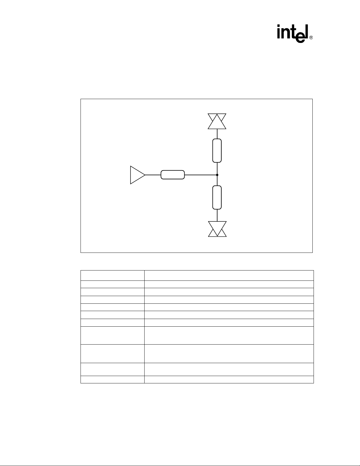
10.1.1 PCI Analog Voltage Filters
The following filter circuit is recommended for the PCI interface. Three separate, identical
versions of this circuit should be placed on the system board, one for each VCCAPCI[2:0] pin on
the 41110.
Figure 22. PCI Analog Voltage Filter Circuit
Serial to
Paralle l P C I
Bridge
Note: Three of these PCI filter circuits must be placed on the system board, one for each of the
VCCAPCI[2:0] pins on the 41110.
• Place C as close as possible to package pin.
• R must be placed between VCC15 and L.
• Route VCCPCI[x] and VSS as differential traces.
• VCCPCI[x] and VSS traces must be ground referenced (No VCC15 references).
• Max total board trace length = 1.2”.
• Min trace space to other nets = 30 mils.
10.1.2 PCI Express Analog Voltage Filter
Figure 23 shows the PCI Express Analog Voltage Circuit.
46 Intel® 41110 Serial to Parallel PCI Bridge Design Guide
Page 47

Figure 23. PCI Express Analog Voltage Filter Circuit
Additional Notes:
• Place C as close as possible to package pin.
• R must be placed between VCC15 and L.
Circuit Implementations
Serial to
Paralle l P CI
Bridge
• Route VCCAPE and VSSAPE as differential traces.
• VCCAPE and VSSAPE traces must be ground referenced (No VCC15 references).
• Max total board trace length = 1.2”.
• Min trace space to other nets = 30 mils.
10.1.3 Bandgap Analog Voltage Filter
Figure 24 shows the Bandgap Analog Voltage Filter Circuit.
Intel® 41110 Serial to Parallel PCI Bridge Design Guide 47
Page 48

Circuit Implementations
Figure 24. Bandgap Analog Voltage Filter Circuit
Additional Notes:
• Place C as close as possible to package pin.
• R must be placed between the 2.5V supply and L.
Serial to
Parallel PCI
Bridge
• Route VCCBGPE and VSSBGPE as differential traces.
• VCCBGPE and VSSBGPE traces must be ground referenced (No 2.5V references).
• VSSBGPE should be grounded at the capacitor.
• Max total board trace length = 1.2”.
• Min trace space to other nets = 30 mils.
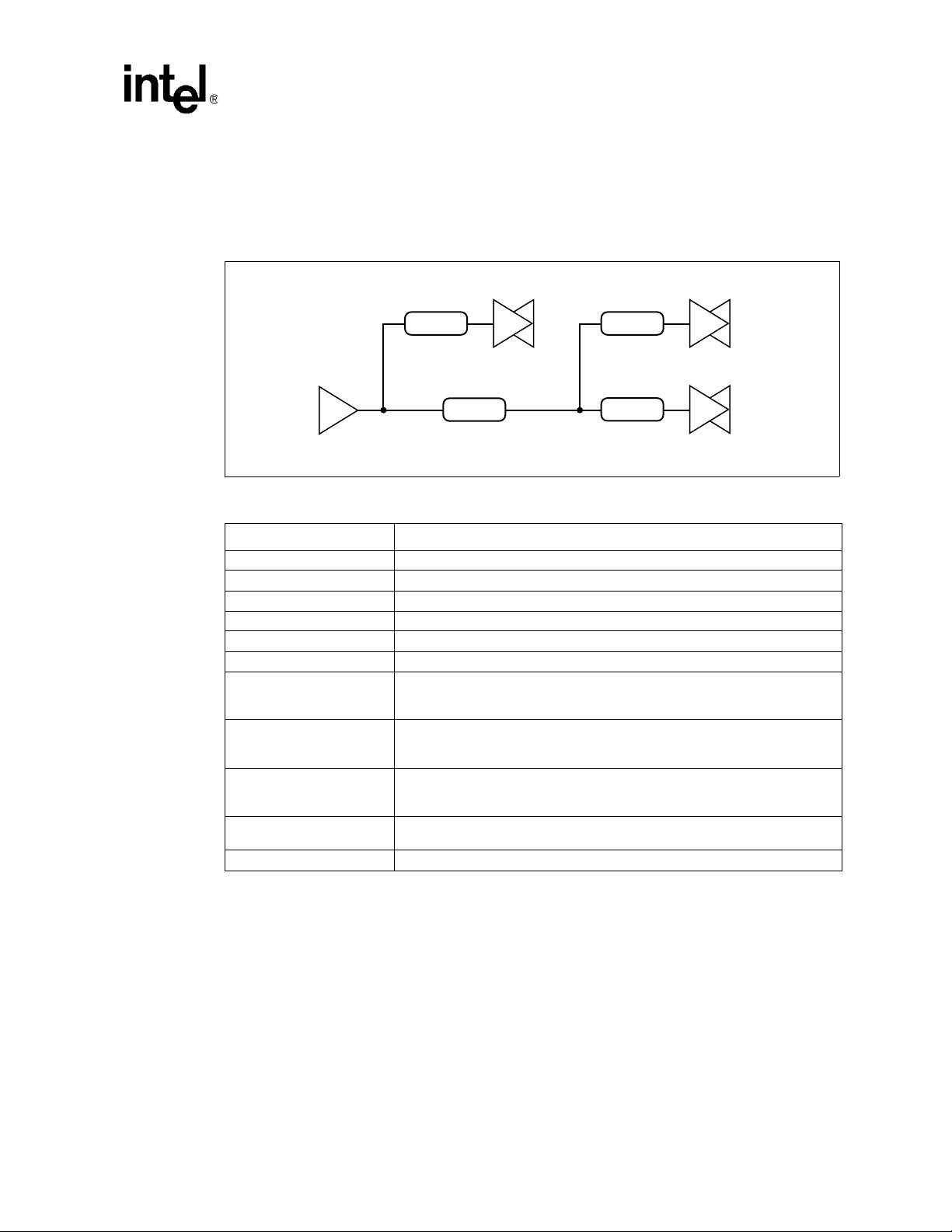
10.2 41110 Reference and Compensation Pins
There are three compensation pins on 41110.
PE_RCOMP[1:0] are two separate pins that provide voltage compensation for the PCI Express
interface on the 41110. The nominal compensation voltage is 0.5V. An external 24.9
resistor should be used to connect to VCC15. A single pullup resistor can be used to for both of
these signals.
RCOMP is an analog PCI interf ace compens ation pin, providin g 0.75V to th e 41110. A 100
pulldown resistor should be used to connect the RCOMP pin to ground.
These implementations are shown in Figure 25.
Ω ±1% pullup
Ω ±1%
48 Intel® 41110 Serial to Parallel PCI Bridge Design Guide
Page 49
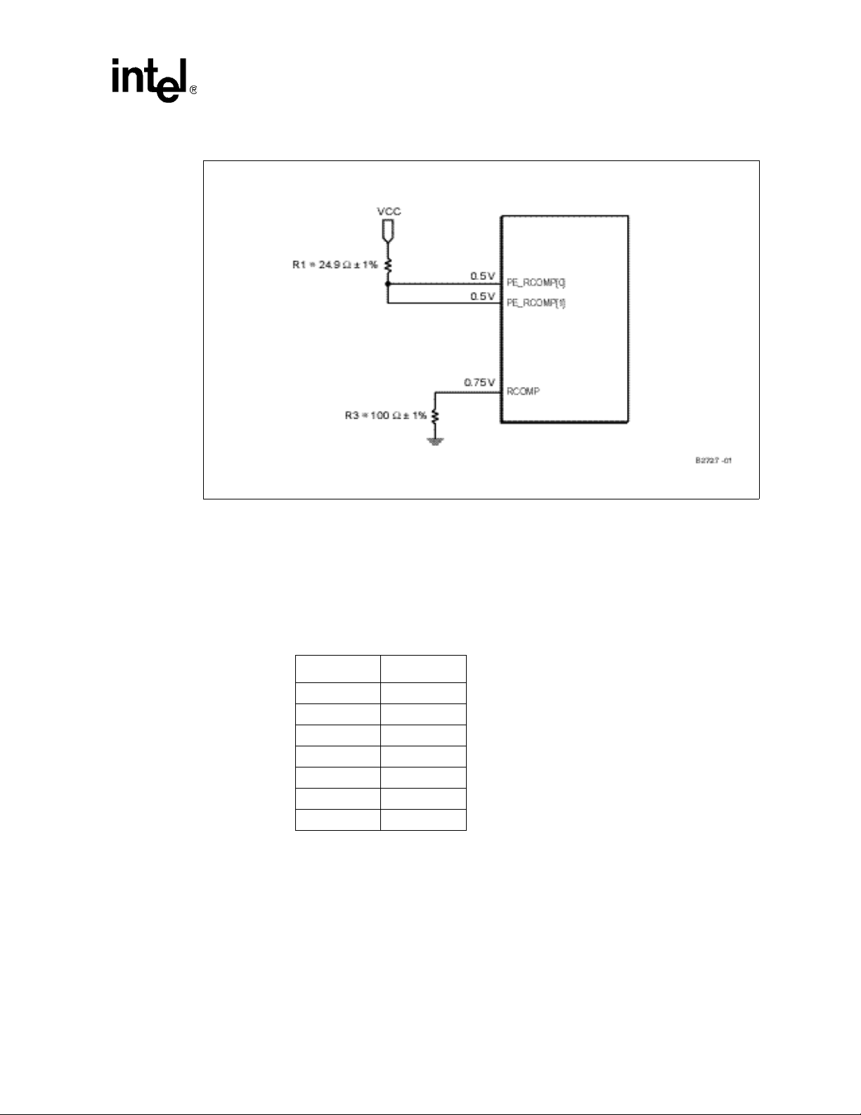
Figure 25. Reference and Compensation Circuit Implementations
Serial to
Paralle l P C I
Bridge
Circuit Implementations
10.2.1 SM Bus
The SMBus interface does not have configuration registers. The SMBus addr ess is set by the states
of pins SMBUS[5] and SMBUS [3: 1] when PERST# is asserted as described in Table 17.
T a ble 17. SMBUs Address Configuration
Refer to Section 2.4 for details on how to use the SMBus to initialize 41110 registers with a
microcontroller.
Bit Value
71
61
5SMBUS[5]
40
3SMBUS[3]
2SMBUS[2]
1SMBUS[1]
Intel® 41110 Serial to Parallel PCI Bridge Design Guide 49
Page 50

Circuit Implementations
This page intentionally left blank.
50 Intel® 41110 Serial to Parallel PCI Bridge Design Guide
Page 51
41110 Customer Reference Boards 11
This chapter describes the 41110 Customer Reference Board (CRB).
11.1 Board Stack-up
The proposed layout of the PCB is eight layers with the following stackup:
• Signal #1 (Top/Component Side)
• Ground Plane: GND
• Signal #2
• Power Plane
• Power Plane
• Signal #3
• Ground Plane
• Signal #4 (Bo t t om)
The permittivity constant Er = 4.5
Table 18. CRB Board Stackup (Sheet 1 of 2)
Layer Type
1 Signal 2.00 1/2 + plating
Prepreg 4.50
2 Plane: GND 1.20 1
Core 4.80
3 Signal 1.20 1
Prepreg 14.00
4 Plane: PWR 1.20 1
Core 3.8
5 Plane: PWR 1.20 1
Prepreg 14.00
6 Signal 1.20 1
Core 4.80
7 Plane: Power 1.20 1
Thickness
(mils)
Copper Weight
Intel® 41110 Serial to Parallel PCI Bridge Design Guide 51
Page 52
41110 Customer Reference Boards
T able 18. CRB Board Stackup (Sheet 2 of 2)
Thickness
11.2 Material
The following materials are used with the 41110 CRB:
• FR-4, 0.062 in. +/- .007, 1.0 oz Copper Power/GND.
• Full length PCI Raw Card (3.3V Universal) 6.2” high x 7.00” long max with ½ inch cut away.
11.3 Impedance
Layer Type
1 Signal 2.00 1/2 + plating
Prepreg 4.50
2 Plane: GND 1.20 1
Core 4.80
3 Signal 1.20 1
Prepreg 4.50
8 Signal 2.00 1/2 + plating
Est. Total
Thickness
(mils)
62 +/- 7
Copper Weight
Most signal layers require controlled Impedance of 60 Ω +/- 5% microstrip or stripline where
appropriate.
Differential signals for the PCI-E interface require matched 100
as matched 50
Ω resistances referenced to ground.
Ω differential termination realized
52 Intel® 41110 Serial to Parallel PCI Bridge Design Guide
Page 53
11.4 Board Outline
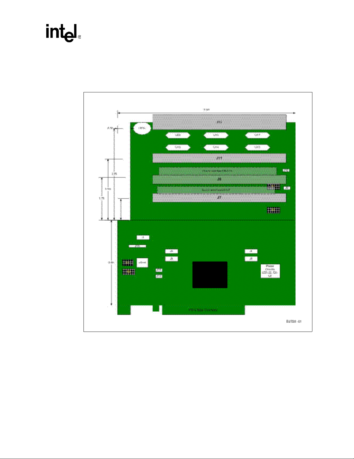
Figure 26 provides the mechanical outline of the 41110 CRB.
Figure 26. Mechanical Outline of the 41110
41110 Customer Reference Boards
U1
Serial to
Parallel PCI
Bridge
Intel® 41110 Serial to Parallel PCI Bridge Design Guide 53
Page 54

41110 Customer Reference Boards
This page intentionally left blank.
54 Intel® 41110 Serial to Parallel PCI Bridge Design Guide
Page 55

Design Guide Checklist 12
This checklist highlights design considerations that should be reviewed prio r to manufacturing an
adapter card that implements the 41110 product. The items contained within this checklist attempt
to address important connections to these devices and any critical supporting circuitry . This is not a
complete list and does not guarantee that a design will function properly.
T able 19. PCI Express Interface Signals
Signals Recommendations Reason/Impact
REFCLKn,
REFCLKp
PE_RCOMP[1:0]
PERP[7:0]
PERN[7:0]
PETP[7:0]
PETN[7:0]
Must be connected to clock from a PCI Express
connector for add-in card designs or to a 100MHz
oscillator for an embedded design.
24.9Ω ±1% pullup resistor to 1.5V . A single resistor can
be used for both signals. Place resistor as close as
possible to REFCLKn, REFCLKp pins.
For X1 mode, only signals PERp[0] and PERn[0] or
PERp[7] and PERn[7] are used.
For X4 mode, only signals PERp[3:0] and PERn[3:0]
are used.
For X8 mode, all of these signals, PERp[7:0] and
PERn[7:0], are used.
For X1 mode, only signals PETp[0] and PETn[0] or
PETp[7] and PETn[7] are used.
For X4 mode, only signals PETP[3:0] and PETN[3:0]
are used.
For X8 mode, all of these signals, PETP[7:0] and
PETN[7:0], are used.
PCI Express compensation pin.
0.5V nominal.
PCI Express data serial inputs
(differential data receive
signals).
PCI Express data serial inputs
(differential data transmit
signals).
Intel® 41110 Serial to Parallel PCI Bridge Design Guide 55
Page 56

Design Guide Checklist
Table 20. PCI/PCI-X Interface Signals (Sheet 1 of 2)
Signals Recommendations Reason/Impact
A_AD[63:32]
A_CBE[7:4]#
A_DEVSEL#
A_FRAME#
A_IRDY#
A_TRDY#
A_STOP#
A_PERR#
A_SERR#
A_REQ[5:0]#
A_GNT[5:0]#
A_LOCK#
A_PAR
A_PAR64
A_ACK64#
A_REQ64#
A_133EN
No external pullup resistors required on system board.
Only relevant when running in PCI-X Mode
(X_PCIXCAP = 1).
Determines the max PCI-X Mode 1 frequency for a
particular segment (100 MHz or 133 MHz):
0 = 100 MHz PCI-X max frequency
1 = 133 MHz PCI-X max frequency
41110 has internal pullup resistors
on these signals.
X_AD[31:0] and X_CBE#[3:0]
signals do not require pullups
according to the PCI Specification.
Sampled on the rising edge of
PERST#.
A_INTA#
A_INTB#
A_INTC#
A_INTD#
Use an 8.2KΩ pullup resistor to VCC33. This resistor is
located on the system board.
No pullup resistors required on these signals.
The 41110 has internal pullup
resistors on these signals.
56 Intel® 41110 Serial to Parallel PCI Bridge Design Guide
Page 57
T able 20. PCI/PCI-X Interface Signals (Sheet 2 of 2)
Signals Recommendations Reason/Impact
Controls frequency of the PCI segment when running
in conventional PCI mode (33 MHz or 66 MHz):
A_M66EN
A_PCIXCAP
0 = 33 MHz PCI
1 = 66 MHz PCI
• Pull-up using a 8.2KΩ resistor when the PCI bus is
to operate at 66 MHz and not already pulled up by
system board. This signal is grounded for 33 MHz
operation.
Connects directly to the PCIXCAP pin on the PCI slot.
Connect to VCC33 through an 8.2KΩ pullup resistor.
Design Guide Checklist
Sampled on the rising edge of
PERST#.
• Design without secondary PCI/PCI-
X Slot
— If there is at least one legacy
PCI device on the PCI/PCI-X
bus, tie this pin directly to
GND.
— If all devices are PCI-X
capable and there is at least
one PCI-X device that only
supports maximum PCI- X
66MHz on the secondary PCI
bus, pull down to GND
through 10K
parallel with a 0.01uF
capacitor.
— If all secondary PCI-X
devices (a nd th e bus lo ading)
support PCI-X 133MHz,
connect PCIXCAP to 3.3V
through an 8.2K
Ω series resistor
Ω resistor
The series resistor on IDSEL should be 200Ω ±5% if it
IDSEL
is exclusively PCIX mode. If it is PCI mode or mixed
PCI/ PCIX mode is intended, 510 ohms is
recommended.
Table 21. Miscellaneous Signals
Signals Recommendations Reason/Impact
RSTIN#
A_STRAP0,
A_STRAP1,
A_STRAP2,
A_STRAP6,
RESERVED [8:1]
Used for debug purposes. Connect to VCC33 through
an 8.2KΩ pullup resistor for normal operation.
These signals REQUIRE external pull-downs to GND
on the board 8.2KΩ unless otherwise stated.
Intel® 41110 Serial to Parallel PCI Bridge Design Guide 57
Page 58

Design Guide Checklist
Table 21. Miscellaneous Signals
Signals Recommendations Reason/Impact
CFGRETRY
A_TEST1,
A_TEST2,
A_PME#,
A_STRAP[3],
A_STRAP[4],
A_STRAP[5],
CMODE This signal requires an external pull-up, 8.2KΩ to 3.3V.
T able 22. SMBus Interface Signals
Signal Recommendations Reason/Impact
SMBCLK Connect to VCC33 through an 8.2KΩ pullup resistor.
SMBDAT Connect to VCC33 through an 8.2KΩ pullup resistor.
SMBUS[5],
SMBUS[3:1]
Input pin to configure 41110 to retry configuration
accesses on it's PCI Express interface.
• T o retry configuration accesses to the 41110, pull high to
3.3V through a 2K
• To allow configuration accesses to the 41110, ground
this pin through a 2K
These signals REQUIRE an external pull-up, 8.2KΩ to
3.3V.
SMBus addressing:
Bit 7----------------’1’
Bit 6----------------’1’
Bit 5---------------SMBUS[5]
Bit 4----------------’0’
Bit 3---------------SMBUS[3]
Bit 2---------------SMBUS[2]
Bit 1---------------SMBUS[1]
Ω resistor.
Ω resistor.
In normal operating mode, this
pin must be tied high.
Sampled on the rising edge of
PERST#.
Use 8.2KΩ resistors as pullups to VCC33 for a ‘1’ and
as pulldowns to ground for a ‘0’ to set the SMBus
address.
58 Intel® 41110 Serial to Parallel PCI Bridge Design Guide
Page 59

T a ble 23. Reset Pins
Ballout Pin Name Usage
E6 STRAP_V_1 Pull up to VCC33
B5 STRAP_V_2 Pull up to VCC33
B3 STRAP_V_3 Pull up to VCC33
A3 STRAP_V_4 Pull up to VCC33
B4 STRAP_V_5 Pull up to VCC33
D4 STRAP_V_6 Pull up to VCC33
F5 STRAP_V_7 Pull up to VCC33
P2 STRAP_V_8 Pull up to VCC33
C3 STRAP_V_9 Pull up to VCC33
D1 STRAP_V_10 Pull up to VCC33
U1 STRAP_V_11 Pull up to VCC33
D7 STRAP_V_12 Pull up to VCC33
U10 STRAP_V_13 Pull up to VCC33
R5 STRAP_V_14 Pull up to VCC33
A19 STRA P_V_15 Pull down to GND
Design Guide Checklist
Intel® 41110 Serial to Parallel PCI Bridge Design Guide 59
Page 60

Design Guide Checklist
Table 24. Power and Ground Signals
Signal Recommendations Reason/Impact
100Ω ±1% (1/4 W) pulldown resistor to ground.
RCOMP
The trace impedance of this signal should be < 0.1Ω.
Connect to 1.5V power supply.
Note: Linear voltage regulators are recommended
when using 1.5 Volt power supplies.
Decoupling:
VCC15
VCC33
VCCAPE
VCCAPCI[2:0] See Figure 22 for circuit. Analog PCI voltage pins.
VCCBGPE
VCCPE
VSS Connect to ground.
VSSAPE See Figure 23 for circuit. Analog ground for PCI Express.
VSSBGPE
5 0.1uF caps beneath package (backside of board)
2 1.0 uF caps as close as design rules permit to
package
3 10 uF caps as close as design rules permit to
package
Connect to 3.3V power supply.
Decoupling: TBD
The platform must insure that the VCC33 voltage rail
be greater than to (or no less than 0.5V below) VCC15
(absolute voltage value at all times during 41110
operation, including during system power up, power
down or any other time during system operation. This
can be accomplished by placing a diode (with a voltage
drop < 0.5V) between VCC15 and VCC33. Anode will
be connected to VCC15 and cathode will be connected
to VCC33.
Connect to 1.5V power supply.
Voltage output of th e bandgap filter circuit into 41110,
separated from the rest of the VCC15s. See Figure 24
for circuit.
Connect to 1.5V power supply.
Decoupling:
• 3 0.1uF caps beneath package (backside of board)
• 4 1.0 uF caps as close as design rules permit to
• 2 10 uF caps as close as design rules permit to
Ground for the bandgap filter circuit, separated from
the rest of the VSSs. See Figure 24 for circuit.
Analog compensation pin for
PCI. 0.75V nominal.
1.5V ±5% core voltage.
3.3V ±5% PCI I/O voltage.
1.5V ±3% Analog PCI Express
voltage.
2.5V ±3% PCI Express voltage.
1.5V ±3% PCI Express voltage.
package
package
Ground reference for all
supplies.
Ground for analog bandgap
voltage.
60 Intel® 41110 Serial to Parallel PCI Bridge Design Guide
Page 61

Table 25. JTAG Signals
Signal Recommendations Reason/Impact
TCK If not used for JTA G, leave as No Connect Internal pull-up
TDI If not used for JTAG, leave as No Connect Internal pull-up
TDO I f not used for JTAG, leave as No Connect Internal pull-up
TMS I f not used for JTAG, leave as No Connect Internal pull-up
TRST# Connect to ground via a 1KΩ pulldown resistor.
If TAP interface is not used this
should be tied to ground.
Page 62

Design Guide Checklist
This page intentionally left blank.
62 Intel® 41110 Serial to Parallel PCI Bridge Design Guide
 Loading...