

Page 1

Intel® 82575EB Gigabit Ethernet
Controller Software Developer’s
Manual and EEPROM Guide
LAN Access Division
324632-003
Revision: 2.1
January 2011
Page 2

Intel® 82575EB Gigabit Ethernet Controller — Legal
Legal
INFORMATION IN THIS DOCUMENT IS PROVIDED IN CONNECTION WITH INTEL® PRODUCTS. NO LICENSE, EXPRESS OR IMPLIED,
BY ESTOPPEL OR OTHERWISE, TO ANY INTELLECTUAL PROPERTY RIGHTS IS GRANTED BY THIS DOCUMENT. EXCEPT AS PROVIDED
IN INTEL'S TERMS AND CONDITIONS OF SALE FOR SUCH PRODUCTS, INTEL ASSUMES NO LIABILITY WHATSOEVER, AND INTEL
DISCLAIMS ANY EXPRESS OR IMPLIED WARRANTY, RELATING TO SALE AND/OR USE OF INTEL PRODUCTS INCLUDING LIABILITY OR
WARRANTIES RELATING TO FITNESS FOR A PARTICULAR PURPOSE, MERCHANTABILITY, OR INFRINGEMENT OF ANY PATENT,
COPYRIGHT OR OTHER INTELLECTUAL PROPERTY RIGHT. Intel products are not intended for use in medical, life saving, life
sustaining, critical control or safety systems, or in nuclear facility applications.
Intel may make changes to specifications and product descriptions at any time, without notice.
Intel Corporation may have patents or pending patent applications, trademarks, copyrights, or other intellectual property rights that
relate to the presented subject matter. The furnishing of documents and other materials and information does not provide any
license, express or implied, by estoppel or otherwise, to any such patents, trademarks, copyrights, or other intellectual property
rights.
Designers must not rely on the absence or characteristics of any features or instructions marked “reserved” or “undefined.” Intel
reserves these for future definition and shall have no responsibility whatsoever for conflicts or incompatibilities arising from future
changes to them.
Intel processor numbers are not a measure of performance. Processor numbers differentiate features within each processor family,
not across different processor families. See http://www.intel.com/products/processor_number for details.
Hyper-Threading Technology requires a computer system with an Intel
HT Technology enabled chipset, BIOS and operating system. Performance will vary depending on the specific hardware and software
you use. See http://www.intel.com/products/ht/Hyperthreading_more.htm for additional information.
Contact your local Intel sales office or your distributor to obtain the latest specifications and before placing your product order.
Copies of documents which have an order number and are referenced in this document, or other Intel literature may be obtained by
calling 1-800-548-4725 or by visiting Intel's website at http://www.intel.com.
Intel and Intel logo are trademarks or registered trademarks of Intel Corporation or its subsidiaries in the United States and other
countries.
*Other names and brands may be claimed as the property of others.
Copyright © 2006,2007,2008,2010.2011; Intel Corporation. All Rights Reserved.
®
Pentium® 4 processor supporting HT Technology and a
Intel® 82575EB Gigabit Ethernet Controller 324632-003
Software Developer’s Manual and EEPROM Guide Revision: 2.1
2 January 2011
Page 3

Revisions — Intel® 82575EB Gigabit Ethernet Controller
Revisions
Revision Date Description
.25 2/2006 Initial release (Intel Secret).
1.1 1/2008 • Updated Section 13.4.8.15 (bit 15 description).
• Updated Table 61 (bit 13 bit description).
.5 6/2006 Major revisions all sections.
1.0 6/2007 Final release (Intel Confidential).
1.2 6/2008 • Updated Section 5.6.1.5 (changed default device ID to 10A7h.
• Updated Section 5.6.1.1 (removed note concerning MAC
addresses).
• Removed table note from Sections 13.7.4 through 13.7.6.
• Updated Sections 13.4.65 and 14.7 concerning COLD field values.
• Updated Section 13.4.8.15 (revised bit 15 description).
• Updated Section 13.4.8.19 (removed statement that D0LPLU can
be loaded from the EEPROM.
• Updated Section 5.6.9 (added new PHY values).
.75 6/2006 Initial release (Intel Confidential).
1.3 9/2008 • Updated Section 13.4.2 (updated SPEED field description; bits
2.0 12/14/2010 • Section 4.1, EEPROM Device - EEPROM size data updated.
2.1 1/28/2011 • Updated brand strings. Updated title.
7:6).
• Replaced device ID table with note to refer to the spec update for
supported device IDs.
• Section 4.5.1.29, PXE Words (Words 30h:3Eh) - Section updated.
Specific field information exposed.
• Section 4.6.4, NC-SI Configuration Structure - Hardware default
values added.
• Section 4.7.2, PBA Number (Words 08h, 09h) - Section updated to
address new methodology.
• Section 5.4.1.3, Association through VLAN tag ID - Added.
• Section 5.4.1.4, Association through VLAN tag ID +RSS - Added.
• Section 10.2.1, Adding 802.1q Tags on Transmits - Section
updated.
• Section 14.3.34, Interrupt Cause Read Register - ICR (000C0H; R)
- Note located in OUTSYNC description updated.
• ASF references removed.
®
324632-003 Intel
Revision: 2.1 Software Developer’s Manual and EEPROM Guide
January 2011 3
82575EB Gigabit Ethernet Controller
Page 4

Intel® 82575EB Gigabit Ethernet Controller — Content
Content
1.0 Introduction ...........................................................................................................................19
1.1 Register and Bit References ........................................................................................................ 19
1.2 Byte and Bit Designations ........................................................................................................... 19
1.3 References ............................................................................................................................... 19
1.4 Memory Alignment Terminology .................................................................................................. 20
2.0 Architectural Overview ...........................................................................................................21
2.1 External Architecture ................................................................................................................. 21
2.1.1 Integrated 10/100/1000 Mb/s PHY......................................................................................... 22
2.1.2 System Interface................................................................................................................. 22
2.1.3 EEPROM Interface ............................................................................................................... 22
2.1.4 Flash Memory Interface........................................................................................................ 23
2.1.5 Management Interfaces........................................................................................................ 23
2.1.5.1 Software Watchdog ....................................................................................................... 23
2.1.6 General-Purpose I/O (Software-Definable Pins) ....................................................................... 23
2.1.7 LEDs.................................................................................................................................. 24
2.1.8 Network Interfaces .............................................................................................................. 24
2.2 DMA Addressing ........................................................................................................................ 24
2.3 Ethernet Addressing................................................................................................................... 25
2.4 Interrupt Control and Tuning....................................................................................................... 26
2.5 Hardware Acceleration Capability ................................................................................................. 26
2.5.1 Jumbo Frame Support.......................................................................................................... 27
2.5.2 Receive and Transmit Checksum Offloading ............................................................................ 27
2.5.3 TCP Segmentation ............................................................................................................... 27
2.5.4 Receive Fragmented UDP Checksum Offloading ....................................................................... 27
2.6 Buffer and Descriptor Structure ...................................................................................................27
2.7 Multiple Transmit Queues ........................................................................................................... 28
2.8 iSCSI Boot................................................................................................................................ 28
3.0 General Initialization and Reset Operation..............................................................................29
3.1 Power Up State ......................................................................................................................... 29
3.2 Initialization Sequence ............................................................................................................... 29
3.3 Interrupts During Initialization..................................................................................................... 29
3.4 Global Reset and General Configuration ........................................................................................ 30
3.5 Receive Initialization .................................................................................................................. 30
3.5.1 Initialize the Receive Control Register ....................................................................................31
3.5.2 Dynamic Queue Enabling and Disabling .................................................................................. 31
3.6 Transmit Initialization ................................................................................................................ 31
3.6.1 Dynamic Queue Enabling and Disabling .................................................................................. 32
3.7 Link Setup Mechanisms and Control/Status Bit Summary ................................................................ 32
3.7.1 PHY Initialization ................................................................................................................. 32
3.7.2 MAC/PHY Link Setup (CTRL_EXT.LINK_MODE = 00b) ............................................................... 32
3.7.3 MAC/SerDes Link Setup (CTRL_EXT.LINK_MODE = 11b)........................................................... 34
3.7.4 MAC/SGMII Link Setup (CTRL_EXT.LINK_MODE = 10b) ............................................................ 35
3.8 Reset Operation ........................................................................................................................ 37
3.8.1 PHY Behavior During a Manageability Session: ........................................................................ 41
3.9 Initialization of Statistics ............................................................................................................ 42
4.0 EEPROM and Flash Interface................................................................................................... 43
4.1 EEPROM Device ......................................................................................................................... 43
4.1.1 Software Accesses............................................................................................................... 43
4.1.2 Signature and CRC Fields ..................................................................................................... 44
4.1.3 EEPROM Recovery ............................................................................................................... 44
4.1.4 Protected EEPROM Space...................................................................................................... 45
4.1.5 Initial EEPROM Programming ................................................................................................ 45
4.1.6 Activating the Protection Mechanism ...................................................................................... 46
4.1.7 Non Permitted Accesses to Protected Areas in the EEPROM ....................................................... 46
4.1.8 EEPROM-Less Support.......................................................................................................... 46
Intel® 82575EB Gigabit Ethernet Controller 324632-003
Software Developer’s Manual and EEPROM Guide Revision: 2.1
4 January 2011
Page 5

Content — Intel® 82575EB Gigabit Ethernet Controller
4.2 Flash Interface Operation ........................................................................................................... 49
4.2.1 Flash Write Control .............................................................................................................. 50
4.2.2 Flash Erase Control.............................................................................................................. 50
4.3 Shared EEPROM ........................................................................................................................ 50
4.3.1 EEPROM Deadlock Avoidance ................................................................................................ 50
4.3.2 EEPROM Map Shared Words.................................................................................................. 51
4.4 Shared FLASH........................................................................................................................... 51
4.4.1 Flash Access Contention ....................................................................................................... 52
4.4.2 Flash Deadlock Avoidance..................................................................................................... 52
4.5 EEPROM Map ............................................................................................................................ 52
4.5.1 Hardware Accessed Words....................................................................................................54
4.5.1.1 Ethernet Address (Words 00h – 02h) ............................................................................... 56
4.5.1.2 Initialization Control 1 (Word 0Ah) .................................................................................. 56
4.5.1.3 Subsystem ID (Word 0Bh) ............................................................................................. 57
4.5.1.4 Subsystem Vendor ID (Word 0Ch)................................................................................... 57
4.5.1.5 Device ID (Word 0Dh, 11h) ............................................................................................ 57
4.5.1.6 Dummy Device ID (Word 1Dh) ....................................................................................... 57
4.5.1.7 Initialization Control 2 (Word 0Fh)................................................................................... 57
4.5.1.8 Software Defined Pins Control (Word 10h)........................................................................ 59
4.5.1.9 EEPROM Sizing & Protected Fields (Word 12h) .................................................................. 60
4.5.1.10 Initialization Control 3 (Word 14h, 24h) ........................................................................... 61
4.5.1.11 NC-SI and PCIe* Completion Timeout Configuration (Word 15h) ......................................... 63
4.5.1.12 MSI-X Configuration (Word 16h) ..................................................................................... 64
4.5.1.13 PLL/Lane/PHY Initialization Pointer (Word 17h) ................................................................. 64
4.5.1.14 PCIe* Initialization Configuration 1 (Word 18h)................................................................. 64
4.5.1.15 PCIe* Initialization Configuration 2 (Word 19h)................................................................. 64
4.5.1.16 Software Defined Pins Control (Word 20h)........................................................................ 65
4.5.1.17 PCIe* Initialization Configuration 3 (Word 1Ah)................................................................. 66
4.5.1.18 PCIe* Control (Word 1Bh) .............................................................................................. 68
4.5.1.19 LED 1, 3 Configuration Defaults (Word 1Ch) ..................................................................... 69
4.5.1.20 Device Revision ID (Word 1Eh) ....................................................................................... 70
4.5.1.21 LED 0, 2 Configuration Defaults (Word 1Fh)...................................................................... 70
4.5.1.22 Functions Control (Word 21h) ......................................................................................... 72
4.5.1.23 LAN Power Consumption (Word 22h) ............................................................................... 72
4.5.1.24 Management Hardware Configuration Control (Word 23h) .................................................. 72
4.5.1.25 End of RO Area (Word 2Ch ............................................................................................. 74
4.5.1.26 Start of RO Area (Word 2Dh) .......................................................................................... 74
4.5.1.27 Watchdog Configuration (Word 2Eh) ................................................................................ 74
4.5.1.28 VPD Pointer (Word 2Fh) ................................................................................................. 74
4.5.1.29 PXE Words (Words 30h:3Eh) .......................................................................................... 74
4.5.1.29.1 Main Setup Options PCI Function 0 (Word 30h) .............................................................. 74
4.5.1.29.2 Configuration Customization Options PCI Function 0 (Word 31h) ...................................... 76
4.5.1.29.3 PXE Version (Word 32h)............................................................................................ 77
4.5.1.29.4 IBA Capabilities (Word 33h) ........................................................................................ 77
4.5.1.29.5 Setup Options PCI Function 1 (Word 34h) ..................................................................... 77
4.5.1.29.6 Configuration Customization Options PCI Function 1 (Word 35h) ...................................... 78
4.5.1.29.7 iSCSI Option ROM Version (Word 36h).......................................................................... 78
4.5.1.29.8 Alternate MAC Address Pointer (Word 37h).................................................................... 78
4.5.1.29.9 Setup Options PCI Function 2 (Word 38h) ..................................................................... 78
4.5.1.29.10 Configuration Customization Options PCI Function 2 (Word 39h) ...................................... 78
4.5.1.29.11 Setup Options PCI Function 3 (Word 3Ah) ..................................................................... 78
4.5.1.29.12 Configuration Customization Options PCI Function 3 (Word 3Bh) ...................................... 78
4.5.1.29.13 iSCSI Boot Configuration Offset (Word 3Dh) .................................................................. 78
4.5.1.29.13.1 iSCSI Module Structure ........................................................................................ 78
4.5.1.29.14 Checksum Word (Word 3Fh)........................................................................................ 80
4.6 Manageability Control Sections .................................................................................................... 81
4.6.1 Sideband Configuration Structure .......................................................................................... 81
4.6.1.1 Section Header - (0ffset 0h) ........................................................................................... 81
4.6.1.2 SMBus Max Fragment Size - (0ffset 01h).......................................................................... 81
4.6.1.3 SMBus Notification Timeout and Flags - (0ffset 02h) .......................................................... 81
®
324632-003 Intel
Revision: 2.1 Software Developer’s Manual and EEPROM Guide
January 2011 5
82575EB Gigabit Ethernet Controller
Page 6

Intel® 82575EB Gigabit Ethernet Controller — Content
4.6.1.4 SMBus Slave Addresses - (0ffset 03h).............................................................................. 81
4.6.1.5 SMBus Fail-Over Register (Low Word) - (0ffset 04h) .......................................................... 83
4.6.1.6 SMBus Fail-Over Register (High Word) - (0ffset 05h) ......................................................... 83
4.6.1.7 NC-SI Configuration (0ffset 06h)..................................................................................... 83
4.6.2 Flex TCO Filter Configuration Structure................................................................................... 83
4.6.2.1 Section Header - (0ffset 0h) ........................................................................................... 83
4.6.2.2 Flex Filter Length and Control - (0ffset 01h) ..................................................................... 85
4.6.2.3 Flex Filter Enable Mask - (0ffset 02 - 09h) ........................................................................ 85
4.6.2.4 Flex Filter Data - (0ffset 0Ah - Block Length) .................................................................... 85
4.6.3 NC-SI Microcode Download Structure ..................................................................................... 85
4.6.3.1 Data Patch Size (Offset 0h) ............................................................................................ 85
4.6.3.2 Rx and Tx Code Size (Offset 1h) ..................................................................................... 85
4.6.3.3 Download Data (Offset 2h - Data Size)............................................................................. 85
4.6.4 NC-SI Configuration Structure............................................................................................... 86
4.6.4.1 Section Header - (0ffset 0h) ........................................................................................... 86
4.6.4.2 Rx Mode Control1 (RR_CTRL[15:0]) (Offset 01h)............................................................... 86
4.6.4.3 Rx Mode Control2 (RR_CTRL[31:16]) (Offset 02h)............................................................. 86
4.6.4.4 Tx Mode Control1 (RT_CTRL[15:0]) (Offset 03h) .............................................................. 86
4.6.4.5 Tx Mode Control2 (RT_CTRL[31:16]) (Offset 04h) ............................................................. 87
4.6.4.6 MAC Tx Control Reg1 (TxCntrlReg1 (15:0]) (Offset 05h) .................................................... 87
4.6.4.7 MAC Tx Control Reg2 (TxCntrlReg1 (31:16]) (Offset 06h) .................................................. 87
4.6.5 Common Firmware Pointer ................................................................................................... 87
4.6.5.1 Manageability Capability/Manageability Enable (Word 54h) ................................................. 88
4.6.6 Pass Through Pointers.......................................................................................................... 88
4.6.6.1 PT LAN0 Configuration Pointer (Word 56h) ....................................................................... 88
4.6.6.2 SMBus Configuration Pointer (Word 57h).......................................................................... 88
4.6.6.3 Flex TCO Filter Configuration Pointer (Word 58h)............................................................... 88
4.6.6.4 PT LAN1 Configuration Pointer (Word 59h) ....................................................................... 90
4.6.6.5 NC-SI Microcode Download Pointer (Word 5Ah)................................................................. 90
4.6.6.6 NC-SI Configuration Pointer (Word 5Bh)........................................................................... 90
4.6.7 PT LAN Configuration Structure .............................................................................................90
4.6.7.1 Section Header (Offset 0h) ............................................................................................. 90
4.6.7.2 LAN0 IPv4 Address 0 LSB, MIPAF0 (Offset 01h)................................................................. 90
4.6.7.3 LAN0 IPv4 Address 0 LSB, MIPAF0 (Offset 02h)................................................................. 90
4.6.7.4 LAN0 IPv4 Address 1; MIPAF1 (Offset 03h:04h) ................................................................ 90
4.6.7.5 LAN0 IPv4 Address 2; MIPAF2 (Offset 05h:06h) ................................................................ 91
4.6.7.6 LAN0 IPv4 Address 3; MIPAF3 (Offset 07h:08h) ................................................................ 91
4.6.7.7 LAN0 MAC Address 0 LSB, MMAL0 (Offset 09h) ................................................................. 91
4.6.7.8 LAN0 MAC Address 0 LSB, MMAL0 (Offset 0Ah) ................................................................. 91
4.6.7.9 LAN0 MAC Address 0 MSB, MMAH0 (Offset 0Bh)................................................................ 91
4.6.7.10 LAN0 MAC Address 1; MMAL/H1 (Offset 0Ch:0Eh) ............................................................. 91
4.6.7.11 LAN0 MAC Address 2; MMAL/H2 (Offset 0Fh:11h).............................................................. 91
4.6.7.12 LAN0 MAC Address 3; MMAL/H3 (Offset 12h:14h) ............................................................. 91
4.6.7.13 LAN0 UDP Flex Filter Ports 0:15; MFUTP Registers (Offset 15h:24h)..................................... 92
4.6.7.14 LAN0 VLAN Filter 0:7; MAVTV Registers (Offset 25h:2Ch)................................................... 92
4.6.7.15 LAN0 Manageability Filters Valid; MFVAL LSB (Offset 2Dh) .................................................. 92
4.6.7.16 LAN0 Manageability Filters Valid; MFVAL MSB (Offset 2Eh) ................................................. 92
4.6.7.17 LAN0 MAC Value MSB (Offset 2Fh) .................................................................................. 93
4.6.7.18 LAN0 MANC Value LSB (Offset 30h) ................................................................................. 93
4.6.7.19 LAN0 Receive Enable 1(Offset 31h) ................................................................................. 93
4.6.7.20 LAN0 Receive Enable 2 (Offset 32h) ................................................................................ 93
4.6.7.21 LAN0 MANC2H Value LSB (Offset 33h) ............................................................................. 95
4.6.7.22 LAN0 MANC2H Value MSB (Offset 34h) ............................................................................ 95
4.6.7.23 Manageability Decision Filters; MDEF0,1 (Offset 35h)......................................................... 95
4.6.7.24 Manageability Decision Filters; MDEF0, 2 (Offset 36h) ........................................................ 96
4.6.7.25 Manageability Decision Filters; MDEF1:6, 1:2 (Offset 37h:42h) ........................................... 96
4.6.7.26 ARP Response IPv4 Address 0 LSB (Offset 43h) ................................................................ 97
4.6.7.27 ARP Response IPv4 Address 0 MSB (Offset 44h)................................................................ 97
4.6.7.28 LAN0 IPv6 Address 0 LSB; MIPAF (Offset 45h) .................................................................. 97
4.6.7.29 LAN0 IPv6 Address 0 MSB; MIPAF (Offset 46h) ................................................................. 97
Intel® 82575EB Gigabit Ethernet Controller 324632-003
Software Developer’s Manual and EEPROM Guide Revision: 2.1
6 January 2011
Page 7

Content — Intel® 82575EB Gigabit Ethernet Controller
4.6.7.30 LAN0 IPv6 Address 0 LSB; MIPAF (Offset 47h) .................................................................. 97
4.6.7.31 LAN0 IPv6 Address 0 MSB; MIPAF (Offset 48h) ................................................................. 97
4.6.7.32 LAN0 IPv6 Address 0 LSB; MIPAF (Offset 49h) .................................................................. 98
4.6.7.33 LAN0 IPv6 Address 0 MSB; MIPAF (Offset 4Ah) ................................................................. 98
4.6.7.34 LAN0 IPv6 Address 0 LSB; MIPAF (Offset 4B).................................................................... 98
4.6.7.35 LAN0 IPv6 Address 0 MSB; MIPAF (Offset 4Ch) ................................................................. 98
4.6.7.36 LAN0 IPv6 Address 1; MIPAF (Offset 4Dh) ........................................................................ 98
4.6.7.37 LAN0 IPv6 Address 2; MIPAF (Offset 55h:5Ch).................................................................. 98
4.7 Software Owned EEPROM Words..................................................................................................98
4.7.1 Compatibility Fields (Word 03h:07h) ...................................................................................... 99
4.7.2 PBA Number (Words 08h, 09h) ............................................................................................. 99
5.0 Receive and Transmit Description......................................................................................... 101
5.1 82575 Data Flows.................................................................................................................... 101
5.1.1 Transmit Data Flow ............................................................................................................101
5.2 Receive Data Flow ................................................................................................................... 102
5.3 Receive Functionality ............................................................................................................... 102
5.3.1 Packet Address Filtering ......................................................................................................103
5.3.2 Receive Data Storage .........................................................................................................103
5.3.3 Legacy Receive Descriptor Format ........................................................................................104
5.3.3.1 Length Field ................................................................................................................104
5.3.3.2 Packet Checksum.........................................................................................................104
5.3.3.3 Receive Descriptor Status Field ...................................................................................... 105
5.3.3.4 Receive Descriptor Errors Field ......................................................................................107
5.3.3.5 VLAN Tag Field ............................................................................................................109
5.3.4 Advanced Receive Descriptors..............................................................................................109
5.3.4.1 Packet Buffer Address................................................................................................... 109
5.3.4.2 Header Buffer Address .................................................................................................. 109
5.3.4.3 Packet Type ................................................................................................................111
5.3.4.4 RSS Type.................................................................................................................... 111
5.3.4.5 Split Header ................................................................................................................ 111
5.3.4.6 Packet Checksum.........................................................................................................112
5.3.4.7 RSS Hash Value ...........................................................................................................113
5.3.4.8 Extended Status ..........................................................................................................113
5.3.4.9 Extended Errors...........................................................................................................114
5.3.4.10 Packet Buffer (Number of Bytes Exists in the Host Packet Buffer) .......................................115
5.3.4.11 VLAN Tag Field ............................................................................................................116
5.3.5 Receive UDP Fragmentation Checksum..................................................................................116
5.3.6 Receive Descriptor Fetching .................................................................................................116
5.3.7 Receive Descriptor Write-Back .............................................................................................117
5.3.7.1 Receive Descriptor Packing............................................................................................ 117
5.3.8 Receive Descriptor Ring Structure.........................................................................................117
5.4 Multiple Receive Queues ........................................................................................................... 119
5.4.1 Queuing for Virtual Machine Devices (VMDq)..........................................................................120
5.4.1.1 Association Through MAC Address ..................................................................................120
5.4.1.2 Association Through MAC Address + RSS ........................................................................121
5.4.1.3 Association through VLAN tag ID.................................................................................... 121
5.4.1.4 Association through VLAN tag ID +RSS ...........................................................................121
5.4.2 Multiple Receive Queues & Receive-Side Scaling (RSS) ............................................................122
5.4.2.1 RSS Hash Function.......................................................................................................122
5.4.2.1.1 Hash for IPv4 with TCP ..............................................................................................124
5.4.2.1.2 Hash for IPv4 with UDP.............................................................................................. 125
5.4.2.1.3 Hash for IPv4 without TCP.......................................................................................... 125
5.4.2.1.4 Hash for IPv6 with TCP ..............................................................................................125
5.4.2.1.5 Hash for IPv6 with UDP.............................................................................................. 125
5.4.2.1.6 Hash for IPv6 without TCP.......................................................................................... 125
5.4.2.2 Indirection Table.......................................................................................................... 125
5.4.2.3 Support for Multiple Processors ...................................................................................... 126
5.4.3 RSS Verification Suite .........................................................................................................126
5.4.3.1 IPv4...........................................................................................................................126
5.4.3.2 IPv6...........................................................................................................................126
®
324632-003 Intel
Revision: 2.1 Software Developer’s Manual and EEPROM Guide
January 2011 7
82575EB Gigabit Ethernet Controller
Page 8

Intel® 82575EB Gigabit Ethernet Controller — Content
5.5 Header Splitting and Replication ................................................................................................ 127
5.5.1 Receive Packet Checksum Offloading ................................................................................... 130
5.5.1.1 MAC Address Filter .......................................................................................................131
5.5.1.2 SNAP/VLAN Filter .........................................................................................................131
5.5.1.3 IPv4 Filter ...................................................................................................................131
5.5.1.4 IPv6 Filter ...................................................................................................................131
5.5.1.5 IPv6 Extension Headers ................................................................................................132
5.5.1.6 UDP/TCP Filter.............................................................................................................133
5.6 Packet Transmission ................................................................................................................ 133
5.6.1 Transmit Data Storage ....................................................................................................... 134
5.6.2 Transmit Contexts ............................................................................................................. 134
5.6.3 Transmit Descriptors.......................................................................................................... 135
5.6.4 Legacy Transmit Descriptor Format...................................................................................... 135
5.6.5 Transmit Descriptor Write Back Format ................................................................................ 136
5.6.5.1 Length........................................................................................................................136
5.6.5.2 Checksum Offset and Start (CSO and CSS)...................................................................... 136
5.6.5.3 Command Byte (CMD) .................................................................................................. 137
5.6.5.4 Transmit Descriptor Status Field Format.......................................................................... 139
5.6.6 Transmit Descriptor Special Field Format .............................................................................. 139
5.6.7 Advanced Transmit Context Descriptor ................................................................................. 140
5.6.7.1 Maximum Segment Size (MSS) Control ...........................................................................141
5.6.8 Advanced Transmit Data Descriptor ..................................................................................... 142
5.6.8.1 Address ......................................................................................................................142
5.6.8.2 DTALEN ......................................................................................................................142
5.6.8.3 DTYP ..........................................................................................................................142
5.6.8.4 DCMD.........................................................................................................................143
5.6.8.5 STA............................................................................................................................144
5.6.8.6 IDX ............................................................................................................................144
5.6.8.7 POPTS ........................................................................................................................ 144
5.6.8.8 PAYLEN.......................................................................................................................144
5.7 Transmit Descriptor Ring Structure ............................................................................................ 144
5.7.1 Transmit Descriptor Fetching .............................................................................................. 146
5.7.2 Transmit Descriptor Write-Back ........................................................................................... 146
5.8 TCP Segmentation ................................................................................................................... 147
5.8.1 Assumptions..................................................................................................................... 148
5.8.2 Transmission Process......................................................................................................... 148
5.8.2.1 TCP Segmentation Data Fetch Control............................................................................. 148
5.8.3 TCP Segmentation Performance .......................................................................................... 148
5.8.4 Packet Format .................................................................................................................. 149
5.8.5 TCP Segmentation Indication .............................................................................................. 149
5.8.6 IP and TCP/UDP Headers .................................................................................................... 151
5.8.7 IP/TCP/UDP Header Updating.............................................................................................. 156
5.8.7.1 TCP/IP/UDP Header for the First Frame ........................................................................... 157
5.8.7.2 TCP/IP/UDP Header for the Subsequent Frames ...............................................................157
5.8.7.3 TCP/IP/UDP Header for the Last Frame ...........................................................................158
5.9 IP/TCP/UDP Transmit Checksum Offloading ................................................................................. 158
5.10 IP/TCP/UDP Transmit Checksum Offloading in Non-Segmentation Mode .......................................... 159
5.10.1 IP Checksum .................................................................................................................... 159
5.10.2 TCP Checksum .................................................................................................................. 160
5.11 Multiple Transmit Queues ......................................................................................................... 160
5.12 Tx Completions Head Write-Back ............................................................................................... 161
5.13 Interrupts............................................................................................................................... 162
5.13.1 Interrupt Cause Register (ICR)............................................................................................ 162
5.13.2 Interrupt Cause Set Register (ICS) ...................................................................................... 163
5.13.3 Interrupt Mask Set/Read Register (IMS) ............................................................................... 163
5.13.4 Interrupt Mask Clear Register (IMC)..................................................................................... 163
5.13.5 Interrupt Acknowledge Auto-mask register (IAM)................................................................... 163
5.13.6 Extended Interrupt Cause Registers (EICR)........................................................................... 163
5.13.7 Extended Interrupt Cause Set Register (EICS)....................................................................... 164
Intel® 82575EB Gigabit Ethernet Controller 324632-003
Software Developer’s Manual and EEPROM Guide Revision: 2.1
8 January 2011
Page 9

Content — Intel® 82575EB Gigabit Ethernet Controller
5.13.8 Extended Interrupt Mask Set and Read Register (EIMS)/Extended Interrupt Mask Clear Register (EIMC)
164
5.13.9 Extended Interrupt Auto Clear Enable Register (EIAC).............................................................164
5.13.10 Extended Interrupt Auto Mask Enable Register (EIAM).............................................................164
5.13.11 Interrupt Modes Setting Bits ................................................................................................165
5.14 Interrupt Moderation................................................................................................................ 165
5.15 Clearing Interrupt Causes ......................................................................................................... 168
5.15.1 Auto-Clear.........................................................................................................................168
5.15.2 Write to Clear ....................................................................................................................169
5.15.3 Read to Clear.....................................................................................................................169
5.16 Dynamic Interrupt Moderation................................................................................................... 169
5.16.1 TCP Timer Interrupt............................................................................................................170
5.17 Memory Error Correction and Detection ...................................................................................... 170
6.0 PCIe* Local Bus Interface..................................................................................................... 173
6.1 General Functionality ............................................................................................................... 173
6.1.1 Message Handling (Receive Side) .........................................................................................173
6.1.2 Message Handling (Transmit Side)........................................................................................173
6.1.3 Data Alignment ..................................................................................................................174
6.1.3.1 4 KB Boundary ............................................................................................................174
6.1.4 Transaction Attributes.........................................................................................................174
6.1.4.1 Traffic Class and Virtual Channels................................................................................... 174
6.1.4.2 Relaxed Ordering ......................................................................................................... 175
6.1.4.3 Snoop Not Required .....................................................................................................175
6.1.4.3.1 No Snoop and Relaxed Ordering for LAN Traffic.............................................................175
6.1.4.3.2 No Snoop Option for Payload ......................................................................................175
6.2 Flow Control ........................................................................................................................... 176
6.2.1 Flow Control Rules..............................................................................................................176
6.2.2 Upstream Flow Control Tracking ...........................................................................................176
6.2.3 Flow Control Update Frequency ............................................................................................177
6.2.4 Flow Control Timeout Mechanism..........................................................................................177
6.2.5 Error Forwarding ................................................................................................................177
6.3 Host Interface......................................................................................................................... 177
6.3.1 Tag IDs.............................................................................................................................177
6.3.2 Completion Timeout Mechanism ...........................................................................................181
6.4 Error Events and Error Reporting ............................................................................................... 182
6.4.1 Error Events ......................................................................................................................182
6.4.2 Error Pollution....................................................................................................................184
6.4.3 Unsuccessful Completion Status ..........................................................................................184
6.4.4 Error Reporting Changes .....................................................................................................184
6.5 Link Layer .............................................................................................................................. 185
6.5.1 ACK/NAK Scheme...............................................................................................................185
6.5.2 Supported DLLPs................................................................................................................185
6.5.3 Transmit EDB Nullifying.......................................................................................................186
6.6 Physical Layer ......................................................................................................................... 186
6.6.1 Link Width.........................................................................................................................186
6.6.1.1 Polarity Inversion.........................................................................................................187
6.6.1.2 L0s Exit latency ...........................................................................................................187
6.6.1.3 Lane-to-Lane De-Skew .................................................................................................187
6.6.1.4 Lane Reversal.............................................................................................................. 187
6.6.1.5 Reset .........................................................................................................................188
6.6.1.6 Scrambler Disable ........................................................................................................188
6.6.2 Performance Monitoring ......................................................................................................188
6.6.3 Configuration Registers .......................................................................................................188
6.6.3.1 PCI Compatibility .........................................................................................................188
6.6.4 Mandatory PCI Configuration Registers.................................................................................. 189
6.6.5 PCI Power Management Registers.........................................................................................195
6.6.5.1 Message Signaled Interrupt (MSI) Configuration Registers .................................................197
6.6.5.2 MSI-X Configuration ..................................................................................................... 198
6.6.5.3 PCIe* Configuration Registers........................................................................................ 201
6.6.5.3.1 PCIe* Extended Configuration Space ...........................................................................210
®
324632-003 Intel
Revision: 2.1 Software Developer’s Manual and EEPROM Guide
January 2011 9
82575EB Gigabit Ethernet Controller
Page 10

Intel® 82575EB Gigabit Ethernet Controller — Content
6.6.5.3.2 Advanced Error Reporting Capability............................................................................211
6.6.5.3.3 Device Serial Number ................................................................................................211
7.0 Power Management .............................................................................................................. 215
7.1 Power States .......................................................................................................................... 215
7.2 Auxiliary Power ....................................................................................................................... 216
7.3 Form Factor Power Limits ......................................................................................................... 216
7.4 Power Management Interconnects ............................................................................................. 217
7.4.0.1 PCIe* Link Power Management ......................................................................................217
7.4.0.2 NC-SI Clock Control .....................................................................................................219
7.4.0.3 PHY Power Management ...............................................................................................219
7.4.0.3.1 Link Speed Control ....................................................................................................219
7.4.0.3.2 D0a State ................................................................................................................220
7.4.0.3.3 Non-D0a State..........................................................................................................221
7.4.0.3.4 Link Energy Detect ....................................................................................................221
7.4.0.3.5 PHY Power-Down State .............................................................................................. 221
7.4.0.3.6 SerDes/SGMII Power-Down State................................................................................222
7.4.1 Power States .................................................................................................................... 222
7.4.1.1 Dr State .....................................................................................................................222
7.4.1.1.1 Dr Disable Mode .......................................................................................................222
7.4.1.1.2 Entry to Dr State ......................................................................................................223
7.4.1.2 D0 Uninitialized State ...................................................................................................223
7.4.1.2.1 Entry to D0u State ....................................................................................................223
7.4.1.3 D0 Active State............................................................................................................224
7.4.1.3.1 Entry to D0a State ....................................................................................................224
7.4.1.4 D3 State .....................................................................................................................224
7.4.1.4.1 Entry to D3 State......................................................................................................224
7.4.1.4.2 Master Disable.......................................................................................................... 225
7.4.1.5 Link-Disconnect ...........................................................................................................225
7.4.2 Power-State Transitions Timing ........................................................................................... 226
7.4.2.1 Power Up (Off to Dup to D0u to D0a).............................................................................. 226
7.4.2.2 Transition from D0a to D3 and Back without PE_RST_N.....................................................227
7.4.2.3 Transition from D0a to D3 and Back with PE_RST_N .........................................................228
7.4.2.4 D0a to Dr and Back without Transition to D3 ...................................................................229
7.4.2.5 Timing Requirements.................................................................................................... 229
7.4.2.6 Timing Guarantees .......................................................................................................230
7.4.3 82575 and SerDes Power-Down State .................................................................................. 230
7.4.3.1 SerDes Power-Down State.............................................................................................230
7.4.3.2 82575 Power-Down State.............................................................................................. 231
7.5 Wake Up ................................................................................................................................ 231
7.5.1 Advanced Power Management Wakeup................................................................................. 231
7.5.2 PCIe Power Management Wakeup........................................................................................ 232
7.5.3 Wake-Up Packets .............................................................................................................. 233
7.5.3.1 Pre-Defined Filters .......................................................................................................233
7.5.3.1.1 Directed Exact Packet ................................................................................................ 233
7.5.3.1.2 Directed Multicast Packet ...........................................................................................233
7.5.3.1.3 Broadcast ................................................................................................................234
7.5.3.1.4 Magic Packet* ..........................................................................................................234
7.5.3.1.5 ARP/IPv4 Request Packet ........................................................................................... 235
7.5.3.1.6 Directed IPv4 Packet .................................................................................................235
7.5.3.1.7 Directed IPv6 Packet .................................................................................................236
7.5.3.2 Flexible Filter...............................................................................................................236
7.5.3.2.1 IPX Diagnostic Responder Request Packet ....................................................................237
7.5.3.2.2 Directed IPX Packet...................................................................................................237
7.5.3.2.3 IPv6 Neighbor Discovery Filter ....................................................................................238
7.5.3.3 Wake Up Packet Storage ............................................................................................... 238
8.0 DCA ...................................................................................................................................... 239
8.1 Implementation Details ............................................................................................................ 239
8.1.1 PCIe* Message Format for DCA (MWr Mode) ......................................................................... 239
Intel® 82575EB Gigabit Ethernet Controller 324632-003
Software Developer’s Manual and EEPROM Guide Revision: 2.1
10 January 2011
Page 11

Content — Intel® 82575EB Gigabit Ethernet Controller
9.0 Ethernet Interface ................................................................................................................ 241
9.1 Internal MAC/PHY 10/100/1000Base-T Interface.......................................................................... 242
9.1.1 MDIO/MDC ........................................................................................................................242
9.2 Duplex Operation for Copper PHY Operation ................................................................................ 243
9.2.1 Full Duplex ........................................................................................................................243
9.2.2 Half Duplex .......................................................................................................................244
9.2.3 Gigabit Physical Coding Sub-Layer (PCS) for SerDes ...............................................................244
9.2.3.1 8B10B Encoding/Decoding ............................................................................................244
9.2.3.2 Code Groups and Ordered Sets ...................................................................................... 245
9.2.4 SGMII Encoding in 10/100 Mb/s ...........................................................................................245
9.3 Auto-Negotiation and Link Setup ............................................................................................... 246
9.3.1 SerDes Link Configuration ...................................................................................................246
9.3.1.1 SerDes Mode Auto-Negotiation ......................................................................................246
9.3.1.2 PCS Hardware Auto-Negotiation ..................................................................................... 247
9.3.1.3 Forcing Link ................................................................................................................ 247
9.3.1.4 Hardware Detection of Non-Auto-Negotiation Partner........................................................248
9.3.1.5 SGMII Auto-Negotiation ................................................................................................ 248
9.3.2 Copper PHY Link Configuration .............................................................................................249
9.3.2.1 PHY Auto-Negotiation (Speed, Duplex, and Flow Control) ..................................................249
9.3.2.2 MAC Speed Resolution .................................................................................................. 249
9.3.2.2.1 Forcing MAC Speed ...................................................................................................249
9.3.2.2.2 Using Internal PHY Direct Link-Speed Indication............................................................250
9.3.2.3 MAC Full/Half Duplex Resolution ....................................................................................250
9.3.2.4 Using PHY Registers .....................................................................................................250
9.3.2.5 Comments Regarding Forcing Link.................................................................................. 251
9.3.3 Loss of Signal/Link Status Indication.....................................................................................251
9.3.4 Flow Control ......................................................................................................................251
9.3.4.1 MAC Control Frames and Reception of Flow Control Packets ............................................... 252
9.3.5 Discard PAUSE Frames and Pass MAC Control Frames .............................................................254
9.3.6 Transmission of PAUSE Frames ............................................................................................254
9.3.7 Software Initiated PAUSE Frame Transmission........................................................................255
9.4 Loopback Support.................................................................................................................... 255
9.4.1 MAC Loopback ...................................................................................................................256
9.4.1.1 Setting the 82575 to MAC Loopback Mode ....................................................................... 256
9.4.2 Internal PHY Loopback ........................................................................................................256
9.4.2.1 Setting the 82575 to Internal PHY Loopback Mode............................................................256
9.4.3 Internal SerDes Loopback....................................................................................................257
9.4.3.1 Setting Internal SerDes Loopback Mode ..........................................................................257
9.4.4 External PHY Loopback........................................................................................................257
9.4.4.1 Setting External PHY Loopback Mode ..............................................................................258
10.0 802.1q VLAN Support............................................................................................................ 259
10.1 802.1q VLAN Packet Format...................................................................................................... 259
10.1.1 802.1q Tagged Frames .......................................................................................................259
10.2 Transmitting and Receiving 802.1q Packets................................................................................. 260
10.2.1 Adding 802.1q Tags on Transmits.........................................................................................260
10.2.2 Stripping 802.1q Tags on Receives .......................................................................................261
10.3 802.1q VLAN Packet Filtering .................................................................................................... 261
10.4 Double VLAN Support............................................................................................................... 262
11.0 PHY Functionality and Features ............................................................................................ 263
11.1 Auto MDIO Register Initialization ............................................................................................... 263
11.1.1 General Register Initialization ..............................................................................................263
11.1.2 Visible Mirror Bit Initialization...............................................................................................263
11.2 Determining Link State............................................................................................................. 264
11.2.1 False Link..........................................................................................................................264
11.2.2 Forced Operation................................................................................................................265
11.2.3 Auto Negotiation ................................................................................................................265
11.2.4 Parallel Detection ...............................................................................................................266
11.2.5 Auto Cross-Over ................................................................................................................266
11.2.5.1 Support for Different Board Layouts ...............................................................................266
®
324632-003 Intel
Revision: 2.1 Software Developer’s Manual and EEPROM Guide
January 2011 11
82575EB Gigabit Ethernet Controller
Page 12

Intel® 82575EB Gigabit Ethernet Controller — Content
11.3 Link Criteria............................................................................................................................ 267
11.3.1 1000BASE-T ..................................................................................................................... 267
11.3.2 100BASE-TX..................................................................................................................... 267
11.3.3 10BASE-T......................................................................................................................... 267
11.4 Link Enhancements.................................................................................................................. 267
11.4.1 SmartSpeed ..................................................................................................................... 267
11.4.1.1 Using SmartSpeed .......................................................................................................268
11.4.2 Flow Control ..................................................................................................................... 268
11.5 Management Data Interface ...................................................................................................... 269
11.6 Low Power Operation ............................................................................................................... 269
11.7 Power Down via the PHY Register .............................................................................................. 269
11.8 1000 Mb/s Operation ............................................................................................................... 269
11.8.1 Transmit Functions ............................................................................................................ 270
11.8.1.1 Scrambler ................................................................................................................... 270
11.8.2 Transmit FIFO................................................................................................................... 271
11.8.2.1 Transmit Phase-Locked Loop PLL.................................................................................... 271
11.8.2.2 Trellis Encoder.............................................................................................................271
11.8.2.3 4DPAM5 Encoder..........................................................................................................271
11.8.2.4 Spectral Shaper ........................................................................................................... 271
11.8.2.5 Low-Pass Filter ............................................................................................................272
11.8.2.6 Line Driver ..................................................................................................................272
11.8.2.7 Transmit/Receive Flow..................................................................................................272
11.8.3 Receive Functions.............................................................................................................. 273
11.8.3.1 Hybrid ........................................................................................................................ 273
11.8.3.2 Automatic Gain Control .................................................................................................273
11.8.3.3 Timing Recovery ..........................................................................................................273
11.8.3.4 Analog-to-Digital Converter ........................................................................................... 273
11.8.3.5 Digital Signal Processor.................................................................................................273
11.8.3.6 Descrambler................................................................................................................ 273
11.8.3.7 Viterbi Decoder/Decision Feedback Equalizer (DFE)...........................................................274
11.8.3.8 4DPAM5 Decoder .........................................................................................................274
11.9 100 Mb/s Operation ................................................................................................................. 274
11.10 10 Mb/s Operation ................................................................................................................... 274
11.10.1 Link Test.......................................................................................................................... 274
11.10.2 10Base-T Link Failure Criteria and Override .......................................................................... 275
11.10.3 Jabber ............................................................................................................................. 275
11.10.4 Polarity Correction............................................................................................................. 275
11.10.5 Dribble Bits ...................................................................................................................... 275
12.0 Configurable LED Outputs..................................................................................................... 277
13.0 Dual Port Characteristics ...................................................................................................... 279
13.1 Features of Each MAC .............................................................................................................. 279
13.1.1 PCIe* Interface................................................................................................................. 279
13.1.2 MAC Configuration Register Space ....................................................................................... 281
13.1.3 SDP, LED, INT# Output...................................................................................................... 281
13.2 Shared EEPROM ...................................................................................................................... 281
13.3 Shared FLASH ......................................................................................................................... 281
13.3.1 FLASH Access Contention ................................................................................................... 281
13.4 Link Mode/Configuration........................................................................................................... 282
13.5 LAN Disable ............................................................................................................................ 282
13.5.1 Overview ......................................................................................................................... 282
13.5.2 Multi-Function Advertisement.............................................................................................. 283
13.5.3 Legacy Interrupt Use ......................................................................................................... 283
13.5.4 Power Reporting................................................................................................................ 283
13.6 Device Disable ........................................................................................................................ 283
13.6.1 BIOS Handling of Device Disable ......................................................................................... 284
13.7 Copper/Fiber Switch................................................................................................................. 284
14.0 Register Descriptions............................................................................................................ 287
14.1 Register Conventions ............................................................................................................... 287
Intel® 82575EB Gigabit Ethernet Controller 324632-003
Software Developer’s Manual and EEPROM Guide Revision: 2.1
12 January 2011
Page 13

Content — Intel® 82575EB Gigabit Ethernet Controller
14.1.1 Memory and I/O Address Decoding .......................................................................................289
14.1.1.1 Memory-Mapped Access to Internal Registers and Memories ..............................................289
14.1.1.2 Memory-Mapped Access to FLASH ..................................................................................289
14.1.1.3 Memory-Mapped Access to MSI-X Tables......................................................................... 289
14.1.1.4 Memory-Mapped Access to Expansion ROM...................................................................... 290
14.1.2 I/O-Mapped Internal Register, Internal Memory, and Flash ......................................................290
14.1.2.1 IOADDR...................................................................................................................... 290
14.1.2.2 IODATA ......................................................................................................................291
14.1.2.3 Undefined I/O Offsets ................................................................................................... 292
14.2 Register Summary................................................................................................................... 292
14.3 Main Register Descriptions ........................................................................................................ 298
14.3.1 Device Control Register - CTRL (00000h; R/W).......................................................................299
14.3.2 Device Status Register - STATUS (00008h; R)........................................................................302
14.3.3 EEPROM/Flash Control Register - EEC (00010h; R/W)..............................................................303
14.3.4 EEPROM Read Register - EERD (00014h; RW) ........................................................................305
14.3.5 Extended Device Control Register - CTRL_EXT (00018h, R/W)..................................................306
14.3.6 Flash Access - FLA (0001Ch; R/W)........................................................................................309
14.3.7 MDI Control Register - MDIC (00020h; R/W)..........................................................................310
14.3.8 PHY Registers ....................................................................................................................311
14.3.8.1 PHY Control Register - PCTRL (00d; R/W)........................................................................ 312
14.3.8.2 PHY Status Register - PSTATUS (01d; R).........................................................................313
14.3.8.3 PHY Identifier Register 1 (LSB) - PHY ID 1 (02d; R) .......................................................... 314
14.3.8.4 PHY Identifier Register 2 (MSB) - PHY ID 2 (03d; R) .........................................................314
14.3.8.5 Auto-Negotiation Advertisement Register - ANA (04d; R/W) ..............................................314
14.3.8.6 Auto-Negotiation Base Page Ability Register - (05d; R)...................................................... 315
14.3.8.7 Auto-Negotiation Expansion Register - ANE (06d; R)......................................................... 316
14.3.8.8 Auto-Negotiation Next Page Transmit Register - NPT (07d; R/W)........................................316
14.3.8.9 Auto-Negotiation Next Page Ability Register - LPN (08d; R)................................................317
14.3.8.10 1000BASE-T/100BASE-T2 Control Register - GCON (09d; R/W) .......................................... 317
14.3.8.11 1000BASE-T/100BASE-T2 Status Register - GSTATUS (10d; R) ..........................................318
14.3.8.12 Extended Status Register - ESTATUS (15d; R) .................................................................319
14.3.8.13 Port Configuration Register - PCONF (16d; R/W) ..............................................................319
14.3.8.14 Port Status 1 Register - PSTAT (17d; RO) ........................................................................320
14.3.8.15 Port Control Register - PCONT (18d; R/W) ....................................................................... 321
14.3.8.16 Link Health Register - LINK (19d; RO) ............................................................................ 322
14.3.8.17 1000Base-T FIFO Register - PFIFO (20d; R/W) ................................................................. 323
14.3.8.18 Channel Quality Register - CHAN (21d; RO) ..................................................................... 324
14.3.8.19 PHY Power Management - (25d; R/W) ............................................................................ 324
14.3.8.20 Special Gigabit Disable Register - (26d; R/W) ..................................................................324
14.3.8.21 Misc Cntrl Register 1 - (27d; R/W) ................................................................................. 325
14.3.8.22 Misc Cntrl Register 2 - (28d; RO) ...................................................................................325
14.3.8.23 Page Select Core Register - (31d; WO) ........................................................................... 326
14.3.9 SERDES ANA - SERDESCTL (00024h; R/W)............................................................................326
14.3.10 Copper/Fiber Switch Control - CONNSW (00034h; R/W) ..........................................................326
14.3.11 VLAN Ether Type - VET (00038h; R/W) .................................................................................327
14.3.12 Fuse Register - UFUSE (5B78h; RO)......................................................................................327
14.3.13 Flow Control Address Low - FCAL (00028h; R/W)....................................................................328
14.3.14 Flow Control Address High - FCAH (0002Ch; R/W) ..................................................................328
14.3.15 Flow Control Type - FCT (00030h; R/W) ................................................................................329
14.3.16 Flow Control Transmit Timer Value - FCTTV (00170h; R/W) .....................................................329
14.3.17 LED Control - LEDCTL (00E00h; RW) ....................................................................................329
14.3.17.1 MODE Encodings for LED Outputs ................................................................................... 330
14.3.18 Packet Buffer Allocation - PBA (01000h; R/W)........................................................................331
14.3.19 Packet Buffer Size - PBS (01008h; R/W)................................................................................332
14.3.20 SFP 12C Command - I2CCMD (01028h; R/W) ........................................................................332
14.3.21 SFP 12C Parameters - I2CPARAMS (0102Ch; R/W) .................................................................333
14.3.22 Flash Opcode - FLASHOP (0103Ch; R/W)...............................................................................334
14.3.23 EEPROM Diagnostic - EEDIAG (01038h; RO) ..........................................................................334
14.3.24 Manageability EEPROM Control Register - EEMNGCTL (01010h; RO) ..........................................335
14.3.25 Manageability EEPROM Read/Write Data - EEMNGDATA (1014h; RO).........................................336
®
324632-003 Intel
Revision: 2.1 Software Developer’s Manual and EEPROM Guide
January 2011 13
82575EB Gigabit Ethernet Controller
Page 14

Intel® 82575EB Gigabit Ethernet Controller — Content
14.3.26 Manageability Flash Control Register - FLMNGCTL (1018h; R/W).............................................. 336
14.3.27 Manageability Flash Read Data - FLMNGDATA (101Ch; R/W) ................................................... 336
14.3.28 Manageability Flash Read Counter - FLMNGCNT (1020h; R/W)................................................. 337
14.3.29 EEPROM Auto Read Bus Control - EEARBC (01024h; R/W) ...................................................... 337
14.3.30 Watchdog Setup - WDSTP (01040h; R/W) ............................................................................ 338
14.3.31 Watchdog SW Device Status - WDSWSTS (01044h; R/W) ....................................................... 338
14.3.32 Free Running Timer - FRTIMER (01048h; RWS) ..................................................................... 339
14.3.33 TCP Timer - TCPTIMER (0104Ch; R/W)................................................................................. 339
14.3.34 Interrupt Cause Read Register - ICR (000C0H; R).................................................................. 340
14.3.35 Interrupt Cause Set Register - ICS (000C8h; WO) ................................................................. 341
14.3.36 Interrupt Mask Set/Read Register - IMS (000D0h; R/W) ......................................................... 342
14.3.37 Interrupt Mask Clear Register - IMC (000D8h; W).................................................................. 343
14.3.38 Interrupt Acknowledge Auto Mask Register - IAM (000E0h; R/W)............................................. 344
14.3.39 Extended Interrupt Cause - EICR (01580h; RC/W1C) ............................................................. 345
14.3.40 Extended Interrupt Cause Set - EICS (01520h; WO) .............................................................. 345
14.3.41 Extended Interrupt Mask Set/Read - EIMS (01524h; RWS) ..................................................... 346
14.3.42 Extended Interrupt Mask Clear - EIMC (01528h; WO)............................................................. 346
14.3.43 Extended Interrupt Auto Clear - EIAC (0152Ch; R/W)............................................................. 347
14.3.44 Extended Interrupt Auto Mask Enable - EIAM (01530h; R/W) .................................................. 347
14.3.45 Interrupt Throttle - EITR (01680h + 4*n [n = 0..9]; R/W) ...................................................... 348
14.3.46 Immediate Interrupt Rx - IMIR (05A80h + 4*n [n = 0..7]; R/W) ............................................. 349
14.3.47 Immediate Interrupt Rx Extended - IMIREXT (05AA0h + 4*n [n = 0..7]; R/W) .......................... 350
14.3.48 Immediate Interrupt Rx VLAN Priority - IMIRVP (05AC0h; R/W)............................................... 350
14.3.49 MSI-X Allocation - MSIXBM (01600h + 4*n [n = 0..9]; R/W)................................................... 351
14.3.50 Receive Control Register - RCTL (00100h; R/W) .................................................................... 351
14.3.51 Split and Replication Receive Control - SRRCTL (0280Ch + 100*n [n=0..3]; R/W) ..................... 354
14.3.52 Packet Split Receive Type - PSRTYPE (05480h + 4*n [n=0..3]; R/W) ....................................... 355
14.3.53 Flow Control Receive Threshold Low - FCRTL (02160h; R/W)................................................... 356
14.3.54 Flow Control Receive Threshold High - FCRTH (02168h; R/W) ................................................. 357
14.3.55 Flow Control Refresh Threshold Value - FCRTV (02460h; R/W) ................................................ 357
14.3.55.1 Receive Descriptor Base Address Low - RDBAL (02800h + 100*n [n=0..3]; R/W) .................358
14.3.56 Receive Descriptor Base Address High - RDBAH (02804h + 100*n [n=0..3]; R/W) ..................... 358
14.3.57 Receive Descriptor Length - RDLEN (02808h + 100*n [n=0..3]; R/W)...................................... 358
14.3.58 Receive Descriptor Head - RDH (02810h + 100*n [n=0..3]; R/W) ........................................... 359
14.3.59 Receive Descriptor Tail - RDT (02818h + 100*n [n=0..3]; R/W) .............................................. 359
14.3.60 Receive Descriptor Control - RXDCTL (02828h + 100*n [n=0..3]; R/W).................................... 360
14.3.61 Receive Checksum Control - RXCSUM (05000h; R/W) ............................................................ 361
14.3.62 Receive Long Packet Maximum Length - RLPML (05004; R/W)................................................. 362
14.3.63 Receive Filter Control Register - RFCTL (05008h; R/W)........................................................... 362
14.3.64 Transmit Control Register - TCTL (00400h; R/W)................................................................... 363
14.3.65 Transmit Control Extended - TCTL_EXT (00404;R/W) ............................................................. 364
14.3.66 Transmit IPG Register - TIPG (00410;R/W)........................................................................... 365
14.3.67 DMA Tx Control - DTXCTL (03590h; R/W)............................................................................. 365
14.3.68 Transmit Descriptor Base Address Low - TDBAL (03800h + 100*n [n=0..3]; R/W) ..................... 366
14.3.69 Transmit Descriptor Base Address High - TDBAH (03804h + 100*n [n=0..3]; R/W).................... 366
14.3.70 Transmit Descriptor Length - TDLEN (03808h + 100*n [n=0..3]; R/W) .................................... 367
14.3.71 Transmit Descriptor Head - TDH (03810h + 100*n [n=0..3]; R/W) .......................................... 367
14.3.72 Transmit Descriptor Tail - TDT (03818h + 100*n [n=0..3]; R/W)............................................. 367
14.3.73 Transmit Descriptor Control - TXDCTL (03828h + 100*n [n=0..3]; R/W) .................................. 368
14.3.74 Tx Descriptor Completion Write-Back Address Low - TDWBAL (03838h + 100*n [n=0..3]; R/W) .. 369
14.3.75 Tx Descriptor Completion Write-Back Address High - TDWBAH (0383Ch + 100*n [n=0..3]; R/W) 370
14.3.76 PCS Configuration 0 - PCS_CFG (04200h; R/W)..................................................................... 370
14.3.77 PCS Link Control - PCS_LCTL (04208h; R/W) ........................................................................ 371
14.3.78 PCS Link Status - PCS_LSTS (0420Ch; R/W)......................................................................... 372
14.3.79 AN Advertisement - PCS_ANADV (04218h; R/W) ................................................................... 373
14.3.80 Link Partner Ability - PCS_LPAB (0421Ch; RO) ...................................................................... 374
14.3.81 Next Page Transmit - PCS_NPTX (04220h; RO) ..................................................................... 375
14.3.82 Link Partner Ability Next Page - PCS_LPABNP (04224h; RO).................................................... 376
14.4 DCA Registers ......................................................................................................................... 376
14.4.1 Rx DCA Control Registers - RXCTL (02814h 100h *n [n=0..3]; R/W)........................................ 376
Intel® 82575EB Gigabit Ethernet Controller 324632-003
Software Developer’s Manual and EEPROM Guide Revision: 2.1
14 January 2011
Page 15

Content — Intel® 82575EB Gigabit Ethernet Controller
14.4.2 Tx DCA Control Registers - TXCTL (03814h + 100h *n [n=0..3]; R/W) ......................................378
14.5 Filter Registers........................................................................................................................ 378
14.5.1 Multicast Table Array - MTA (05200h + 4*n [n..127]; R/W) .....................................................379
14.5.2 Receive Address Low - RAL (05400h + 8*n [n=0..15]; R/W)....................................................380
14.5.3 Receive Address High - RAH (05404h + 8*n [n=0..15]; R/W) ..................................................380
14.5.4 VLAN Filter Table Array - VFTA (05600h + 4*n [n=0..127]; R/W) .............................................381
14.5.5 Multiple Receive Queues Command Register - MRQC (05818h; R/W).........................................382
14.5.6 Redirection Table - RETA (05C00h + 4*n [n=0..31]; R/W).......................................................383
14.5.7 RSS Random Key Register - RSSRK (05C80h + 4*n [n=0..9]; R/W)..........................................384
14.5.8 VMDq Control - VMD_CTRL (0581Ch; R/W)............................................................................384
14.5.9 VLAN Filter Queue Array 0 - VFQA0 (0B100h + 4*n [n=0…127]; R/W) ......................................385
14.5.10 VLAN Filter Queue Array 1 - VFQA1 (0B200h + 4*n [n=0…127]; R/W) ......................................385
14.6 Wakeup Registers.................................................................................................................... 385
14.6.1 Wakeup Control Register - WUC (05800h; R/W) .....................................................................385
14.6.2 Wakeup Filter Control Register - WUFC (05808h; R/W)............................................................386
14.6.3 Wakeup Status Register - WUS (05810h; R/W1C)...................................................................387
14.6.4 IP Address Valid - IPAV (5838h; R/W)...................................................................................387
14.6.5 IPv4 Address Table - IP4AT (05840h + 8*n [n=0..3]; R/W) .....................................................388
14.6.6 IPv6 Address Table - IP6AT (05880h + 4*n[n=0..3]; R/W) ......................................................388
14.6.7 Wakeup Packet Length - WUPL (05900h; RC).........................................................................389
14.6.8 Wakeup Packet Memory (128 Bytes) - WUPM (05A00h + 4*n [n=0..31]; RC).............................389
14.6.9 Flexible Filter Mask Table - FFMT (09000h + 8*n [n=0..127]; R/W) ..........................................389
14.6.10 Flexible Filter Value Table - FFVT (09800h + 8*n [n=0..127]; R/W) ..........................................390
14.6.11 Flexible Filter Length Table - FFLT (05F00h + 8*n [n=0..3]; R/W) ............................................390
14.7 Manageability Registers............................................................................................................ 391
14.7.1 Management VLAN TAG Value - MAVTV (5010h +4*n [n=0..7]; R/W) .......................................391
14.7.2 Management Flex UDP/TCP Ports - MFUTP (5030h + 4*n [n=0..7]; R/W)...................................392
14.7.3 Management Control Register - MANC (05820h; R/W).............................................................392
14.7.4 Manageability Filters Valid - MFVAL (5824h; R/W)...................................................................393
14.7.5 Management Control to Host Register - MANC2H (5860h; R/W)................................................394
14.7.6 Manageability Decision Filters- MDEF (5890h + 4*n [n=0..7]; R/W)..........................................394
14.7.7 Manageability IP Address Filter - MIPAF (0x58B0-0x58EC; RW) ................................................395
14.7.8 Manageability MAC Address Low - MMAL (5910h + 8*n[n=0..3]; RW) .......................................398
14.7.9 Manageability MAC Address High - MMAH (0x5914 + 8*n[n=0..3]; RW) ....................................398
14.7.10 Flexible TCO Filter Table Registers - FTFT (09400h-097FCh; RW)..............................................398
14.7.11 Legacy Sensor Polling Mask 1...8 Register (F8h:FFh)...............................................................400
14.8 PCIe* Registers....................................................................................................................... 400
14.8.1 PCIe* Control - GCR (05B00h; R).........................................................................................400
14.8.2 Function Tag - FUNCTAG (05B08h; R/W) ...............................................................................403
14.8.3 PCIe* Statistics Control #1 - GSCL_1 (05B10h; R) .................................................................403
14.8.4 PCIe* Statistics Control #2 - GSCL_2 (05B14h; R) .................................................................403
14.8.5 PCIe* Statistics Control #3 - GSCL_3 (05B18h; R/W) .............................................................407
14.8.6 PCIe* Statistics Control #4 - GSCL_4 (05B1Ch; R/W) .............................................................407
14.8.7 PCIe* Counter #0 - GSCN_0 (05B20h; R/W) .........................................................................407
14.8.8 PCIe* Counter #1 - GSCN_1 (05B24h; R/W) .........................................................................407
14.8.9 PCIe* Counter #2 - GSCN_2 (05B28h; R/W) .........................................................................408
14.8.10 PCIe* Counter #3 - GSCN_3 (05B2Ch; R/W) .........................................................................408
14.8.11 Function Active and Power State to MNG - FACTPS (05B30h; R) ...............................................408
14.8.12 SerDes/CCM/PCIe* CSR - GIOANACTL0 (05B34h; R/W) ..........................................................409
14.8.13 SerDes/CCM/PCIe* CSR - GIOANACTL1 (05B38h; R/W) ..........................................................409
14.8.14 GIOANACTL2 (05B3Ch; R/W)............................................................................................... 409
14.8.15 GIOANACTL3 (05B40h; R/W) ...............................................................................................410
14.8.16 SerDes/CCM/PCIe* CSR - GIOANACTLALL (05B44h; R/W) .......................................................410
14.8.17 SerDes/CCM/PCIe* CSR - CCMCTL (05B48h; R/W) .................................................................410
14.8.18 SerDes/CCM/PCIe* CSR - SCCTL (05B4Ch; R/W)....................................................................410
14.8.19 Software Semaphore - SWSM (05B50h; R/W) ........................................................................411
14.8.20 Firmware Semaphore - FWSM (05B58h; R/WS) ......................................................................411
14.8.21 Software-Firmware Synchronization - SW_FW_SYNC (05B5Ch; R/WS) ......................................413
14.8.21.1 Using the Software-Firmware Synchronization Register .....................................................413
14.8.22 Mirrored Revision ID - MREVID (05B64h; R/W).......................................................................415
®
324632-003 Intel
Revision: 2.1 Software Developer’s Manual and EEPROM Guide
January 2011 15
82575EB Gigabit Ethernet Controller
Page 16

Intel® 82575EB Gigabit Ethernet Controller — Content
14.8.23 MSI-X PBA Clear - PBACL (05B68h; R/W1C).......................................................................... 415
14.8.24 DCA Requester ID Information - DCA_ID (05B70h; R/W)........................................................ 415
14.8.25 DCA Control - DCA_CTRL (05B74h; R/W) ............................................................................. 416
14.9 Statistics Registers .................................................................................................................. 416
14.9.1 CRC Error Count - CRCERRS (04000h; RC) ........................................................................... 416
14.9.2 Alignment Error Count - ALGNERRC (04004h; RC) ................................................................. 417
14.9.3 Symbol Error Count - SYMERRS (04008h; RC)....................................................................... 417
14.9.4 RX Error Count - RXERRC (0400Ch; RC) ............................................................................... 417
14.9.5 Missed Packets Count - MPC (04010h; RC) ........................................................................... 417
14.9.6 Single Collision Count - SCC (04014h; RC) ........................................................................... 418
14.9.7 Excessive Collisions Count - ECOL (04018h; RC).................................................................... 418
14.9.8 Multiple Collision Count - MCC (0401Ch; RC)......................................................................... 418
14.9.9 Late Collisions Count - LATECOL (04020h; RC)...................................................................... 418
14.9.10 Collision Count - COLC (04028h; RC) ................................................................................... 418
14.9.11 Defer Count - DC (04030h; RC)........................................................................................... 419
14.9.12 Transmit with No CRS - TNCRS (04034h; RC) ....................................................................... 419
14.9.13 Receive Length Error Count - RLEC (04040h; RC) .................................................................. 419
14.9.14 XON Received Count - XONRXC (04048h; RC)....................................................................... 419
14.9.15 XON Transmitted Count - XONTXC (0404Ch; RC)................................................................... 420
14.9.16 XOFF Received Count - XOFFRXC (04050h; RC)..................................................................... 420
14.9.17 XOFF Transmitted Count - XOFFTXC (04054h; RC)................................................................. 420
14.9.18 FC Received Unsupported Count - FCRUC (04058h; RC) ......................................................... 420
14.9.19 Packets Received (64 Bytes) Count - PRC64 (0405Ch; RC)...................................................... 421
14.9.20 Packets Received (65-127 Bytes) Count - PRC127 (04060h; RC) ............................................. 421
14.9.21 Packets Received (128-255 Bytes) Count - PRC255 (04064h; RC)............................................ 421
14.9.22 Packets Received (256-511 Bytes) Count - PRC511 (04068h; RC)............................................ 421
14.9.23 Packets Received (512-1023 Bytes) Count - PRC1023 (0406Ch; RC) ........................................ 422
14.9.24 Packets Received (1024 to Max Bytes) Count - PRC1522 (04070h; RC) .................................... 422
14.9.25 Good Packets Received Count - GPRC (04074h; RC)............................................................... 422
14.9.26 Broadcast Packets Received Count - BPRC (04078h; RC) ........................................................ 423
14.9.27 Multicast Packets Received Count - MPRC (0407Ch; RC) ......................................................... 423
14.9.28 Good Packets Transmitted Count - GPTC (04080h; RC) .......................................................... 423
14.9.29 Good Octets Received Count - GORCL (04088h; RC)/GORCH (0408Ch; RC)............................... 424
14.9.30 Good Octets Transmitted Count - GOTCL (04090h; RC)/ GOTCH (04094; RC)............................ 424
14.9.31 Receive No Buffers Count - RNBC (040A0h; RC) .................................................................... 424
14.9.32 Receive Undersize Count - RUC (040A4h; RC) ....................................................................... 425
14.9.33 Receive Fragment Count - RFC (040A8h; RC)........................................................................ 425
14.9.34 Receive Oversize Count - ROC (040ACh; RC) ........................................................................ 425
14.9.35 Receive Jabber Count - RJC (040B0h; R) .............................................................................. 425
14.9.36 Management Packets Received Count - MNGPRC (040B4h; RC) ............................................... 426
14.9.37 Management Packets Dropped Count - MPDC (040B8h; RC) .................................................... 426
14.9.38 Management Packets Transmitted Count - MNGPTC (040BCh; RC) ........................................... 426
14.9.39 Total Octets Received - TORL (040C0h; RC) / TORH (040C4h; RC)........................................... 427
14.9.40 Total Octets Transmitted - TOTL (040C8h; RC / TOTH (040CCh; RC)........................................ 427
14.9.41 Total Packets Received - TPR (040D0h; RC) .......................................................................... 427
14.9.42 Total Packets Transmitted - TPT (040D4h; RC)...................................................................... 428
14.9.43 Packets Transmitted (64 Bytes) Count - PTC64 (040D8h; RC) ................................................. 428
14.9.44 Packets Transmitted (65-127 Bytes) Count - PTC127 (040DCh; RC)......................................... 428
14.9.45 Packets Transmitted (128-255 Bytes) Count - PTC255 (040E0h; RC)........................................ 429
14.9.46 Packets Transmitted (256-511 Bytes) Count - PTC511 (040E4h; RC)........................................ 429
14.9.47 Packets Transmitted (512-1023 Bytes) Count - PTC1023 (040E8h; RC) .................................... 429
14.9.48 Packets Transmitted (1024 Bytes or Greater) Count - PTC1522 (040ECh; RC) ........................... 429
14.9.49 Multicast Packets Transmitted Count - MPTC (040F0h; RC) ..................................................... 430
14.9.50 Broadcast Packets Transmitted Count - BPTC (040F4h; RC) .................................................... 430
14.9.51 TCP Segmentation Context Transmitted Count - TSCTC (040F8h; RC) ...................................... 430
14.9.52 Interrupt Assertion Count - IAC (04100h; RC)....................................................................... 431
14.9.53 Rx Packets to Host Count - RPTHC (04104h; RC)................................................................... 431
14.9.54 Transmit Queue Empty Count - TXQEC (04118h; RC)............................................................. 431
14.9.55 Receive Descriptor Minimum Threshold Count - RXDMTC (04120h; RC) .................................... 431
14.9.56 Interrupt Cause Receiver Overrun Count - ICRXOC (04124h; RC) ............................................ 431
Intel® 82575EB Gigabit Ethernet Controller 324632-003
Software Developer’s Manual and EEPROM Guide Revision: 2.1
16 January 2011
Page 17

Content — Intel® 82575EB Gigabit Ethernet Controller
14.9.57 SerDes/SGMII Code Violation Packet Count - SCVPC (04228h; R/WS) .......................................432
14.10 Diagnostics Registers ............................................................................................................... 432
14.10.1 Receive Data FIFO Head Register - RDFH (02410h; RO) ..........................................................432
14.10.2 Receive Data FIFO Tail Register - RDFT (02418h; RO) .............................................................432
14.10.3 Receive Data FIFO Head Saved Register - RDFHS (02420h; RO) ...............................................433
14.10.4 Receive Data FIFO Tail Saved Register - RDFTS (02428h; RO)..................................................433
14.10.5 Receive Data FIFO Packet Count - RDFPCQ (02430h + 4 *n [n=0..3]; RO).................................433
14.10.6 PB Descriptor Read Pointers - PBDESCRP (02454h; RO) ..........................................................434
14.10.7 Packet Buffer Diagnostic - PBDIAG (02458h; R/W)..................................................................434
14.10.8 Transmit Data FIFO Head Register - TDFH (03410h; RO) .........................................................434
14.10.9 Transmit Data FIFO Tail Register - TDFT (03418h; R/WS)........................................................435
14.10.10 Transmit Data FIFO Head Saved Register - TDFHS (03420h; R/WS) ..........................................435
14.10.11 Transmit Data FIFO Tail Saved Register - TDFTS (03428h; R/WS).............................................435
14.10.12 Transmit Data FIFO Packet Count - TDFPC (03430h; RO).........................................................436
14.10.13 Packet Buffer ECC Error Inject - PBEEI (03438h; RO) ..............................................................436
14.10.14 Tx Descriptor Handler ECC Error Inject - TDHEEI (035F8h; R/W) ..............................................437
14.10.15 Rx Descriptor Handler ECC Error Inject - RDHEEI (025F8h; R/W)..............................................437
14.10.16 Packet Buffer Memory - PBM (10000h - 10FFCh; R/W) ............................................................438
14.10.17 Packet Buffer Memory Page NPBMPN Register Bit Description ...................................................438
14.10.18 Rx Descriptor Handler Memory Page Number - RDHMP (025FCh; R/W) ......................................438
14.10.19 Tx Descriptor Handler Memory Page Number - TDHMP (035FCh; R/W) ......................................439
14.10.20 Packet Buffer ECC Status - PBECCSTS (0245Ch; R/W).............................................................440
14.10.21 Rx Descriptor Handler ECC Status - RDHESTS (02468h; R/W) ..................................................440
14.10.22 Tx Descriptor Handler ECC Status - TDHESTS (0246Ch; R/W) ..................................................441
14.11 Packet Generator Registers ....................................................................................................... 441
14.11.1 Packet Generator Destination Address Low - PGDAL (04280h; R/W)..........................................441
14.11.2 Packet Generator Destination Address High - PGDAH (04284h; R/W) ........................................441
14.11.3 Packet Generator Source Address Low - PGSAL (04288h; R/W) ................................................442
14.11.4 Packet Generator Source Address High - PGSAH (0428Ch; R/W)...............................................442
14.11.5 Packet Generator Inter Packet Gap - PGIPG (04290h; R/W) .....................................................442
14.11.6 Packet Generator Packet Length - PGPL (04294h; R/W)...........................................................443
14.11.7 Packet Generator Number of Packets - PGNP (04298h; R/W)....................................................443
14.11.8 Packet Generator StaPGSTS Bit Description ...........................................................................444
14.11.9 Packet Generator ContPGCTL Bit Description..........................................................................444
14.12 MSI-X Registers ...................................................................................................................... 445
14.12.1 MSI-X Table Entry Lower Address - MSIXTADD (00000h - 00090h; R/W) ...................................446
14.12.2 MSI-X Table Entry Upper Address - MSIXTUADD (BAR3: 0004h + n*10h [n=0..9]; RW) ..............446
14.12.3 MSI-X Table Entry Message - MSIXTMSG (BAR3: 0008h + n*10h [n=0..9]; RW) ........................446
14.12.4 MSI-X Table Entry Vector Control - MSIXVCTRL (BAR3: 000Ch + n*10h [n=0..9]; RW) ...............446
14.12.5 MSI-X Pending Bit Array - MSIXPBA Bit Description.................................................................447
15.0 Diagnostics and Testability................................................................................................... 449
15.1 Diagnostics............................................................................................................................. 449
15.1.1 FIFO Pointer Accessibility ....................................................................................................449
15.1.2 FIFO Data Accessibility........................................................................................................449
15.1.3 Loopback Operations ..........................................................................................................449
15.2 Testability .............................................................................................................................. 450
15.2.1 EXTEST Instruction.............................................................................................................450
15.2.2 SAMPLE/PRELOAD Instruction ..............................................................................................450
15.2.3 IDCODE Instruction ............................................................................................................450
15.2.4 BYPASS Instruction ............................................................................................................451
16.0 Statistics .............................................................................................................................. 453
16.1 IEEE 802.3 Clause 30 Management ............................................................................................ 453
16.2 OID_GEN_STATISTICS ............................................................................................................. 454
16.3 RMON .................................................................................................................................... 455
16.4 Linux net_device_stats............................................................................................................. 455
®
324632-003 Intel
Revision: 2.1 Software Developer’s Manual and EEPROM Guide
January 2011 17
82575EB Gigabit Ethernet Controller
Page 18

Intel® 82575EB Gigabit Ethernet Controller — Content
NOTE: This page intentionally left blank.
Intel® 82575EB Gigabit Ethernet Controller 324632-003
Software Developer’s Manual and EEPROM Guide Revision: 2.1
18 January 2011
Page 19

Introduction — Intel® 82575EB Gigabit Ethernet Controller
1.0 Introduction
This document describes the external architecture (including device operation, register definitions, etc.)
for the 82575, a Gigabit Ethernet (GbE) network interface controller.
For introduction to the 82575EB and for an overview, see the Intel® 82575EB GbE Controller
Datasheet.
1.1 Register and Bit References
This document refers to device register names with all capital letters. To refer to a specific bit in a
register the convention REGISTER.BIT is used. For example CTRL.FD refers to the Full Duplex Mode bit
in the Device Control Register (CTRL).
1.2 Byte and Bit Designations
This document uses “B” to abbreviate quantities of bytes. For example, a 4 KB represents 4096 bytes.
Similarly, “b” is used to represent quantities of bits. For example, 100 Mb/s represents 100 Megabits
per second.
1.3 References
Intel references include the following manuals:
• Intel® 82575EB Gigabit Ethernet Controller Datasheet
• Intel® 82575EB Gigabit Ethernet Controller Design Guide
• Intel® 82575EB Gigabit Ethernet Controller Manageability
• Intel® 82575EB Gigabit Ethernet Controller Software Developer's Manual and EEPROM Guide
• Intel® 82575EB Gigabit Ethernet Controller Thermal Design Considerations
• Intel® 82575EB Gigabit Ethernet Controller Specification Update
Industry references include:
• IEEE standard 802.3, 2002 Edition (Ethernet). Incorporates various IEEE Standards previously
published separately. Institute of Electrical and Electronic Engineers (IEEE).
• IEEE standard 1149.1, 2001 Edition (JTAG). Institute of Electrical and Electronics Engineers (IEEE)
• PCI Express* Base Specification, Rev.1.1RD, November 2004
®
324632-003 Intel
Revision: 2.1 Software Developer’s Manual and EEPROM Guide
January 2011 19
82575EB Gigabit Ethernet Controller
Page 20

Intel® 82575EB Gigabit Ethernet Controller — Memory Alignment Terminology
• PCI Express* Card Electromechanical Specification, Rev 1.1RD, November 2004
• PICMG3.1 Ethernet/Fiber Channel Over PICMG 3.0 Draft Specification, September 4, 2002, Version
0.90.
• Advanced Configuration and Power Interface Specification, Rev 2.0b, October 2002
• PCI Bus Power Management Interface Specification, Rev. 1.2, March 2004
• PCI Local Bus Specification Revision 2.3 MSI-X ECN
1.4 Memory Alignment Terminology
Some 82575 data structures have special memory alignment requirements. This implies that the
starting physical address of a data structure must be aligned as specified in this manual. The following
terms are used for this purpose:
• BYTE alignment: Implies that the physical addresses can be odd or even. Examples: 0FECBD9A1h,
02345ADC6h.
• WORD alignment: Implies that physical addresses must be aligned on even boundaries. For
example, the last nibble of the address can only end in 0, 2, 4, 6, 8, Ah, Ch, or Eh (0FECBD9A2h).
• DWORD (Double-Word) alignment: Implies that the physical addresses can only be aligned on 4byte boundaries. For example, the last nibble of the address can only end in 0, 4, 8, or Ch
(0FECBD9A8h).
• QWORD (Quad-Word) alignment: Implies that the physical addresses can only be aligned on 8byte boundaries. For example, the last nibble of the address can only end in 0 or 8 (0FECBD9A8h).
• PARAGRAPH alignment: Implies that the physical addresses can only be aligned on 16-byte
boundaries. For example, the last nibble must be a 0 (02345ADC0h).
§ §
Intel® 82575EB Gigabit Ethernet Controller 324632-003
Software Developer’s Manual and EEPROM Guide Revision: 2.1
20 January 2011
Page 21

Architectural Overview — Intel® 82575EB Gigabit Ethernet Controller
2.0 Architectural Overview
This section provides an overview of the 82575. The following sections give detailed information about
the 82575’s functionality, register description, and initialization sequence. All major interfaces of the
82575 is described in detail.
The following principles shaped the design of the 82575:
1. Provide an Ethernet interface containing a 10/100/1000Mb/s PHY that also supports 1000 Base-X
implementations.
2. Provide the highest performance solution possible, based on the following:
— Provide direct access to all memory without using mapping registers
— Minimize the PIO accesses required to manage the 82575
— Minimize the interrupts required to manage the 82575
— Off-load the host processor from simple tasks such as TCP checksum calculations
— Maximize PCIe* efficiency and performance
3. Provide a simple software interface for basic operations.
4. Provide a highly configurable design that can be used effectively in different environments.
2.1 External Architecture
Figure 1 shows the external interfaces to the 82575.
®
324632-003 Intel
Revision: 2.1 Software Developer’s Manual and EEPROM Guide
January 2011 21
82575EB Gigabit Ethernet Controller
Page 22
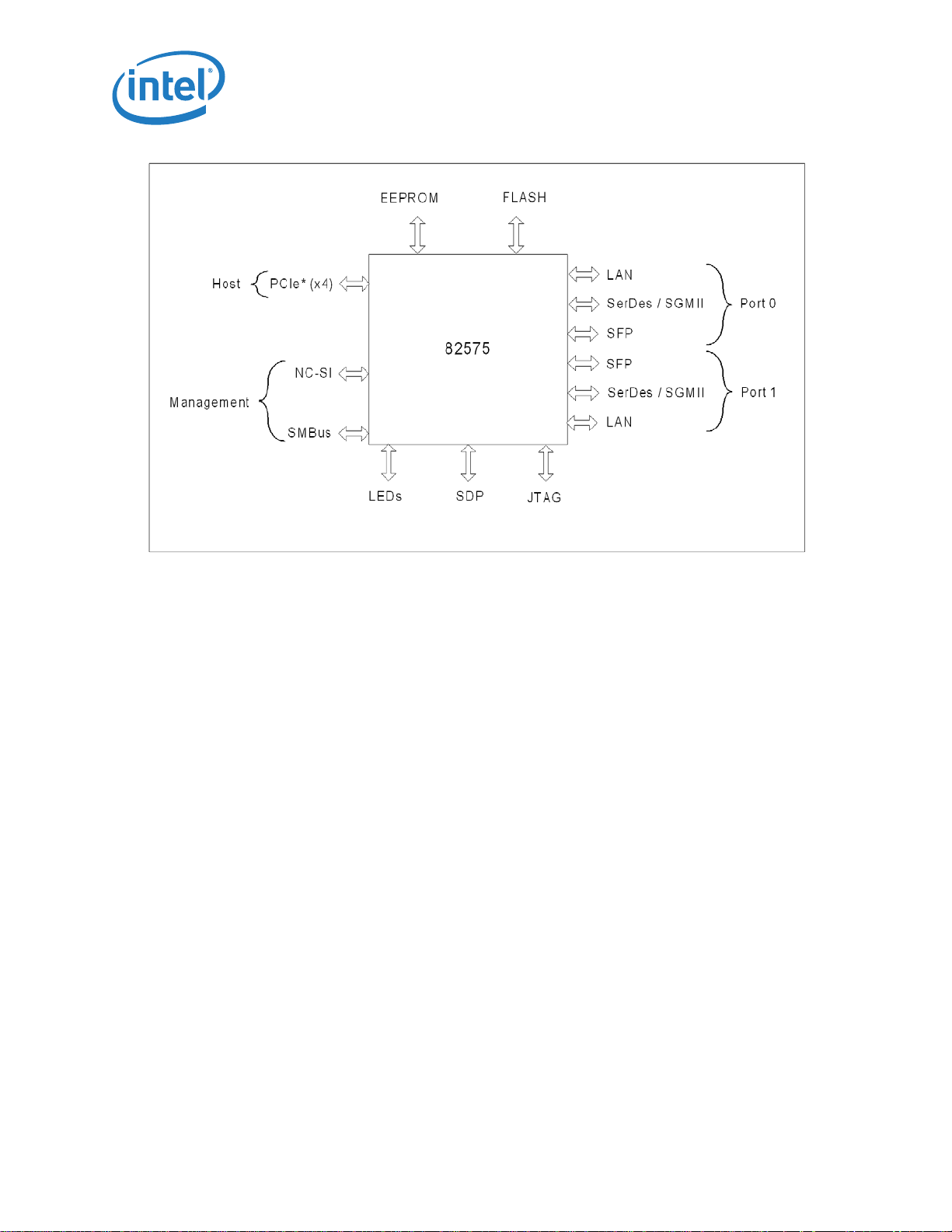
Intel® 82575EB Gigabit Ethernet Controller — Integrated 10/100/1000 Mb/s PHY
Figure 1. 82575 External Interfaces
2.1.1 Integrated 10/100/1000 Mb/s PHY
The 82575 contains integrated 10/100/1000 Mb/s-capable Copper PHY's. Each of these PHY's
communicate with its MAC controllers using a standard 10/100/1000Base-T interface internal to the
component to transfer transmit and receive data. A standard MDIO interface, accessible to software via
MAC control registers, is also used to configure and monitor each PHY operation.
2.1.2 System Interface
The 82575 provides 4 lanes of PCIe* bus interface working at 2.5 GHz each, this should provide
sufficient bandwidth to support sustained dual port of 1000 Mb/s transfer rates. 48 KB of on-chip
buffering mitigates instantaneous receive bandwidth demands and eliminates transmit under-runs by
buffering the entire outgoing packet prior to transmission.
2.1.3 EEPROM Interface
The 82575 provides a four-wire direct interface to a serial EEPROM device such as the 93C46 or
compatible for storing product configuration information. Several words of the data stored in the
EEPROM are automatically accessed by the 82575, after reset, to provide pre-boot configuration data to
the 82575 before it is accessible by the host software. The remainder of the stored information is
accessed by various software modules to report product configuration, serial number and other
parameters.
Note: An EEPROM is required for normal operation.
Intel® 82575EB Gigabit Ethernet Controller 324632-003
Software Developer’s Manual and EEPROM Guide Revision: 2.1
22 January 2011
Page 23

Flash Memory Interface — Intel® 82575EB Gigabit Ethernet Controller
2.1.4 Flash Memory Interface
The 82575 provides an external serial interface to a FLASH device. Accesses to the FLASH are
controlled by the 82575 and are accessible to software as normal PCIe* reads or writes to the FLASH
memory mapping area. The 82575 supports FLASH devices with up to 512 KB of memory
2.1.5 Management Interfaces
The 82575 contains two possible interfaces to an external BMC.
• SMBus
•NC-SI
Since the manageability sideband throughput is lower than the network link throughput, the 82575
allocates an 8 KB internal buffer for incoming network packets prior to being send over the sideband
interface. Refer to the 82575 System Management Bus Interface Application Note for detailed
information about the management interface.
2.1.5.1 Software Watchdog
In some situations it might be useful to give an indication to the manageability firmware or to external
devices that the 82575 hardware or the driver is not functional. In order to provide this functionality, a
watchdog mechanism is used. This mechanism can be enabled by default, according to the EEPROM
configuration. Once the host driver is up and it determines hardware is functional, it might reset the
watchdog timer to indicate the device is functional. The software device driver then should re-arm the
timer periodically. If the timer is not re-armed after a pre-programmed timeout, an interrupt is given to
firmware and a pre-programmed SDP is raised. The SDP indication is shared between the ports.
The register controlling this feature is WDSETUP. This register enables setting the timeout period and
the activation of this mode. Both get their default from the EEPROM.
The re-arming of the timer is done by setting the WDSWSTS.Dev_functional.
If software needs to trigger the watchdog immediately because it suspects hardware is stuck, it can set
the WDSWSTS.Force_WD bit. It can also give firmware an indication if the watchdog reason using the
WDSWSTS.stuck_reason field.
The SDP that provides the watchdog indication is set using the CTRL.SDP0_WDE. In this mode the
CTRL.SDP0_IODIR should be set to output. The CTRL.SDP0_DATA bit indicates the polarity of the
indication. Setting this bit in one of the cores causes the watchdog indications of both cores to be
indicated on this SDP.
2.1.6 General-Purpose I/O (Software-Definable Pins)
The 82575 has four software-defined pins (SDP pins) per port that can be used for miscellaneous
hardware or software-controllable purposes. These pins and their function are bound to a specific LAN
device (for example, eight SDP pins might not be associated with a single LAN device). These pins can
each be individually configurable to act as either input or output pins. The default direction of each of
®
324632-003 Intel
Revision: 2.1 Software Developer’s Manual and EEPROM Guide
January 2011 23
82575EB Gigabit Ethernet Controller
Page 24

Intel® 82575EB Gigabit Ethernet Controller — LEDs
the four pins is configurable via EEPROM as well as the default value of any pins configured as outputs.
To avoid signal contention, all four pins are set as input pins until after the EEPROM configuration is
loaded.
The use, direction, and values of SDP pins are controlled and accessed using fields in the Device Control
register (CTRL) and Extended Device Control register (CTRL_EXT).
2.1.7 LEDs
The 82575 provides four LEDs per port that can be used to indicate different traffic status. The default
setup of the LEDs is done via the EEPROM words 1Ch and 1Fh. The default setup for both ports is the
same. This setup is reflected in the LEDCTL register of each port. Each software device driver can
change its setup individually. For each of the LEDs the following parameters can be defined:
• Mode: Defines which information is reflected by this LED. The encoding is described in the LEDCTL
register.
• Polarity: Defines the polarity of the LED.
• Blink mode: should the LED blink or be stable.
In addition, the blink rate of all LEDs can be defined. The possible rates are 200 ms or 83 ms for each
phase. There is one rate for all LEDs.
2.1.8 Network Interfaces
The 82575 MAC provides a complete CSMA/CD function that supports IEEE 802.3
(10 Mb/s), 802.3u (100 Mb/s), 802.3z and 802.3ab (1000 Mb/s) implementations. The 82575 performs
all of the functions required for transmission, reception, and collision handling called out in the
standards.
Each 82575 MAC can be configured to be used as a different media interface. While the most likely
application is expected to be based on use of the internal copper PHY, the 82575 supports the following
potential configurations:
• Internal copper PHY
• External SerDes device such as an optical SerDes (SFP or onboard) or backplane connections.
• External SGMII device. This mode is used for SFP connections or external SGMII PHYs.
Selection between the various configurations is programmable via each MAC's Extended Device Control
register (CTRL_EXT.LINK_MODE bits) and defaulted via EEPROM settings.
2.2 DMA Addressing
In appropriate systems, all addresses mastered by the 82575 are 64 bits in order to support systems
that have larger than 32-bit physical addressing. Providing 64-bit addresses eliminates the need for
special segment registers.
Note: Descriptor accesses are not byte swapped.
The following example illustrates data-byte ordering. Bytes for a receive packet arrive in the order
shown from left to right.
Intel® 82575EB Gigabit Ethernet Controller 324632-003
Software Developer’s Manual and EEPROM Guide Revision: 2.1
24 January 2011
Page 25
Ethernet Addressing — Intel® 82575EB Gigabit Ethernet Controller
01 02 03 04 05 06 07 08 09 0a 0b 0c 0d 0e 0f 10 11 12 13 14 15 16 17 18 19 1a 1b 1c 1d 1e
Example 1. Byte Ordering
There are no alignment restrictions on packet-buffer addresses. The byte address for the major words
is shown on the left. The byte numbers and bit numbers for the PCIe* bus are shown across the top.
Table 1. Little Endian Data Ordering
Byte
Address
00807060504030201
8100f 0e0d0c0b0a09
10 18 17 16 15 14 13 12 11
18 20 1f 1e 1d 1c 1b 1a 19
63 0
76543210
2.3 Ethernet Addressing
Several registers store Ethernet addresses in the 82575. Two 32-bit registers make up the address: one
is called “high”, and the other is called “low”. For example, the Receive Address Register is comprised of
Receive Address High (RAH) and Receive Address Low (RAL). The least significant bit of the least
significant byte of the address stored in the register (for example, bit 0 of RAL) is the multicast bit. The
LS byte is the first byte to appear on the wire. This notation applies to all address registers, including
the flow control registers.
Figure 2 shows the bit/byte addressing order comparison between what is on the wire and the values in
the unique receive address registers.
Preamble & SFD Destination Address Source Address
...55 D5 00 11 22 33 ...XXX00 AA
Bit 0 of this byte is first on the wire
dest_addr[0]
2233 00AA0011
Destination address stored
internally as shown here
...
33
001122
00AA
Multicast bit
Figure 2. Example of Address Byte Ordering
The address byte order numbering shown in Figure 2 maps to Table 2. Byte #1 is first on the wire.
®
324632-003 Intel
Revision: 2.1 Software Developer’s Manual and EEPROM Guide
January 2011 25
82575EB Gigabit Ethernet Controller
Page 26

Intel® 82575EB Gigabit Ethernet Controller — Interrupt Control and Tuning
Table 2. Intel® Architecture Byte Ordering
IA Byte # 1 (LSB) 2 3 4 5 6 (MSB)
Byte Value (Hex) 00 AA 00 11 22 33
Note: The notation in this manual follows the convention shown in Table 2. For example, the
address in Table 2 indicates 00_AA_00_11_22_33h, where the first byte (00h_) is the first
byte on the wire, with bit 0 of that byte transmitted first.
2.4 Interrupt Control and Tuning
The 82575 provides a complete set of interrupts that allow for efficient software management. The
interrupt structure is designed to accomplish the following:
• Make accesses “thread-safe” by using ‘set’ and ‘clear-on-read’ rather than ‘read-modify-write’
operations.
• Correlate between related bits in different registers (for example, ICR)
• Minimize the number of interrupts needed relative to work accomplished.
• Minimize the processing overhead associated with each interrupt.
The interrupt logic consists of the interrupt registers that are described in sections 14.3.34 through
14.3.37.
Two actions minimize the number of interrupts:
1. Reducing the frequency of all interrupts
2. Accepting multiple receive packets before signaling an interrupt.
One interrupt register consolidates all interrupt information eliminating the need for multiple accesses.
Note: The 82575 supports Message Signaled Interrupts per the PCI 2.2, 2.3, and PCIe*
specifications. See Section 4.7.5.1 for details.
2.5 Hardware Acceleration Capability
The 82575 provides the ability to offload IP, TCP, and UDP checksum for transmit. The functionality
provided by these features can significantly reduce processor utilization by shifting the burden of the
functions from the driver to the hardware. Features include:
• Jumbo frame support
• Receive and transmit checksum offloading
• TCP segmentation
• Receive fragmented UDP checksum offload
• These features are briefly outlined in the following sections.
Intel® 82575EB Gigabit Ethernet Controller 324632-003
Software Developer’s Manual and EEPROM Guide Revision: 2.1
26 January 2011
Page 27

Jumbo Frame Support — Intel® 82575EB Gigabit Ethernet Controller
2.5.1 Jumbo Frame Support
The 82575 supports jumbo frames to increase performance and decrease CPU utilization. By default,
the 82575 might receive packets with a maximum size of 1522 bytes. If large frame reception is
enabled by the RCTL register, the 82575 supports jumbo packet reception of up to 9018 bytes
(including CRC and headers). On the transmit size, jumbo packets are always supported by the 82575.
It is the responsibility of the software device driver to initiate jumbo packets only when it is configured
to do so.
2.5.2 Receive and Transmit Checksum Offloading
The 82575 provides the ability to offload the IP, TCP, and UDP checksum requirements from the
software device driver. For common frame types, the hardware automatically calculates, inserts, and
checks the appropriate checksum values normally handled by software.
For transmits where the 82575 is doing non-TCP segmentation, every transmitted Ethernet packet can
have two checksums calculated and inserted by the 82575. Typically these would be the IPv4 and either
TCP or UDP checksums. The software device driver specifies which portions of the packet are included
in the checksum calculations, and where the calculated values are inserted, via descriptor(s).
For receives, the hardware recognizes the packet type and performs the checksum calculations as well
as error checking automatically. Checksum and error information is provided to software via the receive
descriptor(s). Refer to Section 5.5.1 for details.
2.5.3 TCP Segmentation
The 82575 implements a TCP segmentation capability for transmits that enables the software device
driver to offload packet segmentation and encapsulation to the hardware. The software device driver
can send the 82575 the entire IP (IPv6 or IPv6), TCP or UDP message sent down by the Network
Operating System (NOS) for transmission. The 82575 segments the packet into legal Ethernet frames
and transmit them on the wire. By handling the segmentation tasks, the hardware alleviates the
software from handling some of the framing responsibilities. This reduces the overhead on the CPU for
the transmission process thus reducing overall CPU utilization.
2.5.4 Receive Fragmented UDP Checksum Offloading
The 82575 provides the ability to offload inbound fragmented UDP packet reassembly. The 82575
provides the partial checksum calculation for each incoming UDP fragment so that the software device
driver is required to sum the partial checksum words for each fragment to produce the complete
checksum. The fragmented UDP checksum offload is provided to IPv4 packets.
2.6 Buffer and Descriptor Structure
Software allocates the transmit and receive buffers, and also forms the descriptors that contain
pointers to, and the status of, those buffers. A conceptual ownership boundary exists between the
driver software and the hardware of the buffers and descriptors.
®
324632-003 Intel
Revision: 2.1 Software Developer’s Manual and EEPROM Guide
January 2011 27
82575EB Gigabit Ethernet Controller
Page 28

Intel® 82575EB Gigabit Ethernet Controller — Multiple Transmit Queues
The software gives the hardware ownership of a queue of buffers for receives. These receive buffers
store data that the software then owns once a valid packet arrives.
For transmits, the software maintains a queue of buffers. The driver software owns a buffer until it is
ready to transmit. The software then commits the buffer to the hardware; the hardware then owns the
buffer until the data is loaded or transmitted in the transmit FIFO.
Descriptors store the following information about the buffers:
• The physical address
• The length
• Status and command information about the referenced buffer
Descriptors contain an end-of-packet field that indicates the last buffer for a packet. Descriptors also
contain packet-specific information indicating the type of packet, and specific operations to perform in
the context of transmitting a packet, such as those for VLAN or checksum offload.
2.7 Multiple Transmit Queues
The 82575 supports four transmit descriptor rings (this matches the expected number of processors on
most server platforms).
The priority between the queues can be set and specified in the memory space. Multiple transmit
queues are intended for the following usage models.
Note: If there are more processors than queues, then one queue can be used to service more
than one processor.
2.8 iSCSI Boot
This feature consists of adding an iSCSI class code to potentially replace the LAN class code of the
ports. When the system is booting, the BIOS detects this class code and runs SCSI software.
The 82575 reads two control bits out of EEPROM. Each bit affects its respective LAN class code value. If
the bit is 0b (this is the current value of the unused bits) the LAN class code remains as it is (value =
020000 = LAN). If the bit is set to 1b, the LAN class code becomes a SCSI class code (value = 010000
= SCSI). Having this functionality enables programmers to change one port (or two in specific
applications) to a SCSI device type and loads an iSCSI miniport driver for that port. This port also
functions as iSCSI HBA. Default values for these fields in the EEPROM for both ports remain as a
network class type.
In this case, the MAC address and the IP address of the port are used by the iSCSI function.
§ §
Intel® 82575EB Gigabit Ethernet Controller 324632-003
Software Developer’s Manual and EEPROM Guide Revision: 2.1
28 January 2011
Page 29

General Initialization and Reset Operation — Intel® 82575EB Gigabit Ethernet Controller
3.0 General Initialization and Reset Operation
This section lists all necessary initializations and describes the reset commands for the 82575.
3.1 Power Up State
When the 82575 powers up, it reads the EEPROM. The EEPROM contains sufficient information to bring
the link up and configure the 82575 for manageability and/or APM wakeup. However, software
initialization is required for normal operation.
3.2 Initialization Sequence
The following sequence of commands is typically issued to the 82575 by the software device driver in
order to initialize the 82575 to normal operation. The major initialization steps are:
• Disable Interrupts - see Interrupts during initialization.
• Issue Global Reset and perform General Configuration - see Global Reset and General
Configuration.
• Setup the PHY and the link - see Link Setup Mechanisms and Control/Status Bit Summary.
• Initialize all statistical counters - see Initialization of Statistics.
• Initialize Receive - see Receive Initialization.
• Initialize Transmit - see Transmit Initialization.
• Enable Interrupts - see Interrupts During Initialization.
3.3 Interrupts During Initialization
Most drivers disable interrupts during initialization to prevent re-entrancy. Interrupts are disabled by
writing to the IMC and EIMC registers. Note that the interrupts also need to be disabled after issuing a
global reset, so a typical driver initialization flow might be:
• Disable interrupts
• Issue a Global Reset
• Disable interrupts (again)
•…
®
324632-003 Intel
Revision: 2.1 Software Developer’s Manual and EEPROM Guide
January 2011 29
82575EB Gigabit Ethernet Controller
Page 30

Intel® 82575EB Gigabit Ethernet Controller — Global Reset and General Configuration
After the initialization completes, a typical driver enables the desired interrupts by writing to the IMS
and EIMS registers.
3.4 Global Reset and General Configuration
The 82575 initialization typically starts with a global reset that puts it into a known state and enables
the software device driver to continue the initialization sequence.
Several values in the Device Control Register (CTRL) need to be set upon power up or after an 82575
reset for normal operation.
• FD should be set per interface negotiation (if done in software), or is set by the hardware if the
interface is Auto-Negotiating. This is reflected in the Device Status Register in the Auto-Negotiating
case.
• Speed is determined via Auto-Negotiation or forced by software if the link is forced. Status
information for speed is also readable in STATUS.
• In SerDes mode, CTRL.ILOS should be set to according to the polarity of the Sig_DET signal.
Set the packet buffer allocation for transmit receive flows in the PBA register. This should be done
before RCTL.RXEN & TCTL.TXEN are set. An ordered disabling of all queues and of the Rx and Tx flows
is required before any change in the packet buffer allocation is done.
If flow control is enabled, program the FCRTL, FCRTH, FCTTV and FCRTV registers.
3.5 Receive Initialization
Program the Receive address register(s) per the station address. This can come from the EEPROM or
from any other means (for example, on some systems, this comes from the system PROM not the
EEPROM on the adapter card)
Set up the MTA (Multicast Table Array) per software by zeroing all entries initially and adding in entries
as requested.
Program RCTL with appropriate values. If initializing it at this stage, it is best to leave the receive logic
disabled (EN = 0b) until after the receive descriptor ring has been initialized. If VLANs are not used,
software should clear VFE. Then there is no need to initialize the VFTA. Select the receive descriptor
type.
The following should be done once per receive queue:
• Allocate a region of memory for the receive descriptor list.
• Receive buffers of appropriate size should be allocated and pointers to these buffers should be
stored in the descriptor ring.
• Program the descriptor base address with the address of the region.
• Set the length register to the size of the descriptor ring.
• Program PSRCTL of the queue according to the size of the buffers and the required header handling
• If header split or header replication is required for this queue, program the PSRTYPE register
according to the required headers.
Intel® 82575EB Gigabit Ethernet Controller 324632-003
Software Developer’s Manual and EEPROM Guide Revision: 2.1
30 January 2011
Page 31

Initialize the Receive Control Register — Intel® 82575EB Gigabit Ethernet Controller
• Enable the queue by setting RXDCTL.ENABLE. In the case of queue zero, the enable bit is set by
default, as such, the ring parameters should be set before RCTL.RXEN is set.
• Program the direction of packets to this queue according to the mode select in MRQC. Packets
directed to a disabled queue are dropped.
3.5.1 Initialize the Receive Control Register
To properly receive packets, the receiver should be enabled by setting RCTL.RXEN. This should be done
only after all other setup is accomplished. If software uses the Receive Descriptor Minimum Threshold
Interrupt, that value should be set.
Note: The Receive Descriptor Tail register of the queue (RDT[n]) should not be bumped until the
queue is enabled. This register must also be written after the queue is enabled and the
receiver is enabled.
3.5.2 Dynamic Queue Enabling and Disabling
Receive queues can be dynamically enabled or disabled provided the following procedure is followed:
Enabling:
• Follow the per queue initialization previously described.
• If there are still packets in the packet buffer directed to this queue according to previous settings,
they are received after the queue is re-enabled. The software device driver might check if old
packets are still in the internal packet buffer by reading the RDFPCQ# register of the queue.
Disabling:
• Disable the direction of packets to this queue.
• Disable the queue by clearing RXDCTL.ENABLE. The 82575 immediately stops to fetch and write
back descriptors from this queue. The 82575 eventually completes the storage of one buffer
allocated to this queue. Any further packet directed to this queue is dropped. If the currently
processed packet is spread over more than one buffer, all subsequent buffers are not written.
• The 82575 clears RXDCTL.ENABLE only after all pending memory accesses to the descriptor ring or
to the buffers are done. The software device drive should poll this bit before releasing the memory
allocated to this queue.
The Rx path can be disabled only after all Rx queues are disabled.
3.6 Transmit Initialization
Program the TCTL register according to the required MAC behavior.
If work in half duplex mode is expected, program the TCTL_EXT.COLD field. For internal PHY mode, the
default value is 41h. For SGMII mode, a value reflecting the 82575 and the PHY SGMII delays should be
used. A suggested value for a typical PHY is 46h for 10 Mb/s and 4Ch for 100 Mb/s.
The following should be done once per transmit queue:
• Allocate a region of memory for the transmit descriptor list.
• Program the descriptor base address with the address of the region.
®
324632-003 Intel
Revision: 2.1 Software Developer’s Manual and EEPROM Guide
January 2011 31
82575EB Gigabit Ethernet Controller
Page 32

Intel® 82575EB Gigabit Ethernet Controller — Dynamic Queue Enabling and Disabling
• Set the length register to the size of the descriptor ring.
• Program the TXDCTL register with the desired TX descriptor write back policy. Suggested values
are:
— WTHRESH = 1b
— All other fields 0b.
• Set the queue priority using TXDCTL.Priority
• Enable the queue using TXDCTL.ENABLE (queue zero is enabled by default).
Enable the transmit path by setting TCTL. This should be done only after all other settings are done.
3.6.1 Dynamic Queue Enabling and Disabling
Transmit queues can be dynamically enabled or disabled provided the following procedure is followed:
Enabling: Follow the per queue initialization previously described.
Disabling:
• Stop storing packet for transmission in this queue.
• Wait until the head of the queue (TDH) is equal to the tail (TDT). For example, the queue is empty.
• Disable the queue by clearing TXDCTL.ENABLE.
The Tx path can be disabled only after all Tx queues are disabled.
3.7 Link Setup Mechanisms and Control/Status Bit Summary
Note: The CTRL_EXT.LINK_MODE value should be set to the desired mode prior to the setting of
the other fields in the link setup procedures.
3.7.1 PHY Initialization
Refer to the PHY documentation for the initialization and link setup steps. The software device driver
uses the MDIC register to initialize the PHY and setup the link.
3.7.2 MAC/PHY Link Setup (CTRL_EXT.LINK_MODE =
00b)
This section summarizes the various means of establishing proper MAC/PHY link setups, differences in
MAC CTRL register settings for each mechanism, and the relevant MAC status bits. The methods are
ordered in terms of preference (the first mechanism being the most preferred).
• MAC settings automatically based on duplex and speed resolved by PHY
(CTRL.FRCDPLX = 0b, CTRL.FRCSPD = 0b)
Intel® 82575EB Gigabit Ethernet Controller 324632-003
Software Developer’s Manual and EEPROM Guide Revision: 2.1
32 January 2011
Page 33

MAC/PHY Link Setup (CTRL_EXT.LINK_MODE = 00b) — Intel® 82575EB Gigabit Ethernet
Controller
CTRL.FD - Don't care; duplex setting is established from PHY's internal indication to the MAC (FDX)
after PHY has auto-negotiated a successful link-up
CTRL.SLU - Must be set to 1b by software to enable communications between MAC and PHY
CTRL.RFCE - Must be set by software after reading flow control resolution from PHY registers
CTRL.TFCE - Must be set by software after reading flow control resolution from PHY registers
CTRL.SPEED - Don't care; speed setting is established from PHY's internal indication to the MAC
(SPD_IND) after PHY has auto-negotiated a successful link-up
STATUS.FD - Reflects the actual duplex setting (FDX) negotiated by the PHY and indicated to MAC
STATUS.LU - Reflects link indication (LINK) from PHY qualified with CTRL.SLU (set to 1b)
STATUS.SPEED - Reflects actual speed setting negotiated by the PHY and indicated to the MAC
(SPD_IND)
• MAC duplex and speed settings forced by software based on resolution of PHY
(CTRL.FRCDPLX = 1b, CTRL.FRCSPD = 1b)
CTRL.FD - Set by software based on reading PHY status register after PHY has auto-negotiated a
successful link-up
CTRL.SLU - Must be set to 1b by software to enable communications between MAC and PHY
CTRL.RFCE - Must be set by software after reading flow control resolution from PHY registers
CTRL.TFCE - Must be set by software after reading flow control resolution from PHY registers
CTRL.SPEED - Set by software based on reading PHY status register after PHY has auto-negotiated a
successful link-up.
STATUS.FD - Reflects the MAC forced duplex setting written to CTRL.FD
STATUS.LU - Reflects link indication (LINK) from PHY qualified with CTRL.SLU (set to 1b)
STATUS.SPEED - Reflects MAC forced speed setting written in CTRL.SPEED
• MAC/PHY duplex and speed settings both forced by software (fully-forced link setup)
(CTRL.FRCDPLX = 1b, CTRL.FRCSPD = 1b, CTRL.SLU = 1b)
CTRL.FD - Set by software to desired full/half duplex operation (must match duplex setting of PHY)
CTRL.SLU - Must be set to 1b by software to enable communications between MAC and PHY. PHY must
also be forced/configured to indicate positive link indication (LINK) to the MAC
CTRL.RFCE - Must be set by software to desired flow-control operation (must match flow-control
settings of PHY)
CTRL.TFCE - Must be set by software to desired flow-control operation (must match flow-control
settings of PHY)
CTRL.SPEED - Set by software to desired link speed (must match speed setting of PHY)
®
324632-003 Intel
Revision: 2.1 Software Developer’s Manual and EEPROM Guide
January 2011 33
82575EB Gigabit Ethernet Controller
Page 34

Intel® 82575EB Gigabit Ethernet Controller — MAC/SerDes Link Setup (CTRL_EXT.LINK_MODE =
STATUS.FD - Reflects the MAC duplex setting written by software to CTRL.FD
STATUS.LU - Reflects 1b. (positive link indication LINK from PHY qualified with CTRL.SLU).
Note: Since both CTRL.SLU and the PHY link indication LINK are forced, this bit set does not
guarantee that operation of the link has been truly established.
STATUS.SPEED - Reflects MAC forced speed setting written in CTRL.SPEED.
11b)
3.7.3 MAC/SerDes Link Setup (CTRL_EXT.LINK_MODE = 11b)
Link setup procedures using an external SerDes interface mode:
• Hardware Auto-Negotiation Enabled (PCS_LCTL.AN_ENABLE = 1b)
CTRL.FD - Ignored; duplex is set by priority resolution of PCS_ANDV and PCS_LPAB.
CTRL.SLU - Ignored; it is not possible to “force” link configuration (AN_ENABLE takes precedence)
CTRL.RFCE - Must be set by software after reading flow control resolution from PCS registers
CTRL.TFCE - Must be set by software after reading flow control resolution from PCS registers
CTRL.SPEED - Ignored; speed always 1000 Mb/s when using SGMII mode communications
STATUS.FD - Reflects hardware-negotiated priority resolution
STATUS.LU - Reflects PCS_LSTS.AN COMPLETE (Auto-Negotiation complete)
STATUS.SPEED - Reflects 1000 Mb/s speed, reporting fixed value of 10b
PCS_LCTL.FORCE_LINK - Ignored; it is not possible to "force" link configuration (AN_ENABLE takes
precedence)
PCS_LCTL.FSD - Ignored; it is not possible to "force" link configuration (AN_ENABLE takes precedence)
PCS_LCTL.FSV - Ignored; speed always 1000Mb/s when using SerDes mode communications
PCS_LCTL.FDV - Ignored; duplex is set by priority resolution of PCS_ANDV and PCS_LPAB
PCS_LCTL.FLV - Ignored; it is not possible to "force" link configuration (AN_ENABLE takes precedence)
• Software-Executed Auto-Negotiation Enabled (PCS_LCTL.AN_ENABLE = 0b)
CTRL.FD - Should be set by software to the duplex value established via software priority resolution
CTRL.SLU - Should be set by software to 1b when software Auto-Negotiation completes
CTRL.RFCE - Set by software as a result of software priority resolution
CTRL.TFCE - Set by software as a result of software priority resolution
CTRL.SPEED - Ignored; speed always 1000 Mb/s when using SerDes mode communications
Intel® 82575EB Gigabit Ethernet Controller 324632-003
Software Developer’s Manual and EEPROM Guide Revision: 2.1
34 January 2011
Page 35

MAC/SGMII Link Setup (CTRL_EXT.LINK_MODE = 10b) — Intel® 82575EB Gigabit Ethernet
Controller
STATUS.FD - Reflects the value written by software to CTRL.FD
STATUS.LU - Reflects whether loss-of-signal (LOS) from SerDes is indicated, qualified with CTRL.SLU
(set to 1b)
STATUS.SPEED - Reflects 1000 Mb/s speed, reporting fixed value of 10b
PCS_LCTL.FORCE_LINK - Must be set to 1b by software to enable communications to the SerDes
PCS_LCTL.FSD - Must be set to 1b by software to enable communications to the SerDes
PCS_LCTL.FSV - Ignored; speed always 1000 Mb/s when using SerDes mode communications.
PCS_LCTL.FDV - Should be set by software to the duplex value established via software priority
resolution
PCS_LCTL.FLV - Should be set by software to 1b when software Auto-Negotiation completes
• Forced-Link (Auto-Negotiation Skipped) (PCS_LCTL. AN ENABLE = 0b, and no software autonegotiation performed)
CTRL.FD - Duplex is set by software for the desired duplex mode of operation
CTRL.SLU - Must be set to 1b by software to enable communications to the SerDes
CTRL.RFCE - Set by software for the desired mode of operation
CTRL.TFCE - Set by software for the desired mode of operation
CTRL.SPEED - Ignored
STATUS.FD - Reflects the value written by software to CTRL.FD
STATUS.LU - Reflects whether loss-of-signal (LOS) from SerDes is indicated, qualified with CTRL.SLU
(set to 1b)
STATUS.SPEED - Reflects 1000 Mb/s speed, reporting fixed value of 10b
PCS_LCTL.FORCE_LINK - Must be set to 1b by software to enable communications to the SerDes
PCS_LCTL.FSD - Must be set to 1b by software to enable communications to the SerDes
PCS_LCTL.FSV - Ignored; speed always 1000 Mb/s when using SerDes mode communications.
PCS_LCTL.FDV - Duplex is set by software for the desired duplex mode of operation.
PCS_LCTL.FLV - Should be set by software to 1b to enable communications to the SerDes
3.7.4 MAC/SGMII Link Setup (CTRL_EXT.LINK_MODE = 10b)
Link setup procedures using an external SGMII interface mode:
®
324632-003 Intel
Revision: 2.1 Software Developer’s Manual and EEPROM Guide
January 2011 35
82575EB Gigabit Ethernet Controller
Page 36

Intel® 82575EB Gigabit Ethernet Controller — MAC/SGMII Link Setup (CTRL_EXT.LINK_MODE =
10b)
• Hardware Auto-Negotiation Enabled (PCS_LCTL. AN ENABLE = 1b,
CTRL.FRCDPLX = 0b, CTRL.FRCSPD = 0b)
CTRL.FD - Ignored; duplex is set by priority resolution of PCS_ANDV and PCS_LPAB.
CTRL.SLU - Ignored; it is not possible to “force” link configuration (AN_ENABLE takes precedence)
CTRL.RFCE - Must be set by software after reading flow control resolution from PCS registers
CTRL.TFCE - Must be set by software after reading flow control resolution from PCS registers
CTRL.SPEED - Don't care; speed setting is established from SGMII's internal indication to the MAC after
SGMII has auto-negotiated a successful link-up
STATUS.FD - Reflects hardware-negotiated priority resolution
STATUS.SPEED - Reflects actual speed setting negotiated by the SGMII and indicated to the MAC
PCS_LCTL.FORCE_LINK - Ignored; it is not possible to "force" link configuration (AN_ENABLE takes
precedence)
PCS_LCTL.FSD - Ignored; it is not possible to "force" link configuration (AN_ENABLE takes precedence)
PCS_LCTL.FSV - Ignored; speed is set by priority resolution of PCS_ANDV and PCS_LPAB
PCS_LCTL.FDV - Ignored; duplex is set by priority resolution of PCS_ANDV and PCS_LPAB
PCS_LCTL.FLV - Ignored; it is not possible to "force" link configuration (AN_ENABLE takes precedence)
• Software-Executed Auto-Negotiation Enabled (PCS_LCTL. AN ENABLE = 0b; CTRL.FRCDPLX = 1b,
CTRL.FRCSPD = 1b)
CTRL.FD - Should be set by software to the duplex value established via software priority resolution
CTRL.SLU - Should be set by software to 1b when software Auto-Negotiation completes
CTRL.RFCE - Set by software as a result of software priority resolution
CTRL.TFCE - Set by software as a result of software priority resolution
CTRL.SPEED - Set by software to desired link speed (must match speed setting of external SGMII PHY)
STATUS.FD - Reflects MAC forced speed setting written in CTRL.SPEED
STATUS.LU - Reflects whether loss-of-signal (LOS) from SerDes is indicated, qualified with CTRL.SLU
(set to 1b)
STATUS.SPEED - Reflects MAC forced speed setting written in CTRL.SPEED
PCS_LCTL.FORCE_LINK - Must be set to 1b by software to enable communications to the SGMII PHY
PCS_LCTL.FSD - Must be set to 1b by software to enable communications to the SGMII PHY
PCS_LCTL.FSV - Set by software to desired link speed (must match speed setting of external SGMII
PHY)
Intel® 82575EB Gigabit Ethernet Controller 324632-003
Software Developer’s Manual and EEPROM Guide Revision: 2.1
36 January 2011
Page 37

Reset Operation — Intel® 82575EB Gigabit Ethernet Controller
PCS_LCTL.FDV - Should be set by software to the duplex value established via software priority
resolution
PCS_LCTL.FLV - Should be set by software to 1b when software Auto-Negotiation completes
• Forced-Link (Auto-Negotiation Skipped) (PCS_LCTL. AN_ENABLE = 0b, and no software autonegotiation performed)
CTRL.FD - Duplex is set by software for the desired duplex mode of operation
CTRL.SLU - Must be set to 1b by software to enable communications to the SerDes
CTRL.RFCE - Set by software for the desired mode of operation
CTRL.TFCE - Set by software for the desired mode of operation
CTRL.SPEED - Set by software to desired link speed (must match speed setting of external SGMII PHY)
STATUS.FD - Reflects the value written by software to CTRL.FD
STATUS.LU - Reflects whether loss-of-signal (LOS) from SerDes is indicated, qualified with CTRL.SLU
(set to 1b)
STATUS.SPEED - Reflects MAC forced speed setting, written in CTRL.SPEED
PCS_LCTL.FORCE_LINK - Must be set to 1b by software to enable communications to the SerDes
PCS_LCTL.FSD - Must be set to 1b by software to enable communications to the SerDes
PCS_LCTL.FSV - Set by software to desired link speed (must match speed setting of external SGMII
PHY and CTRL.SPEED)
PCS_LCTL.FDV - Duplex is set by software for the desired duplex mode of operation (must match
duplex setting of external SGMII PHY and CTRL.FD)
PCS_LCTL.FLV - Must be set by software to 1b to enable communications to the SerDes
3.8 Reset Operation
The 82575’s reset sources are as follows:
PE_RST_N:
Asserting PE_RST_N indicates that both the power and the PCIe* clock sources are stable. This pin
asserts an internal reset also after a D3cold exit. Most units are reset on the rising edge of PE_RST_N.
The only exception is the GIO unit, which is kept in reset while PE_RST_N is deasserted (level).
Inband PCIe* Reset:
The 82575 generates an internal reset in response to a Physical layer message from the PCIe* or when
the PCIe* link goes down (entry to Polling or Detect state). This reset is equivalent to PCI reset in
previous (PCI) gigabit LAN controllers.
®
324632-003 Intel
Revision: 2.1 Software Developer’s Manual and EEPROM Guide
January 2011 37
82575EB Gigabit Ethernet Controller
Page 38

Intel® 82575EB Gigabit Ethernet Controller — Reset Operation
D3hot to D0 Transition:
This is also known as ACPI Reset. The 82575 generates an internal reset on the transition from D3hot
power state to D0 (caused after configuration writes from D3 to D0 power state). Note that this reset is
per function and resets only the function that transitioned from D3hot to D0.
Software Reset:
Software can reset the 82575 by writing the Device Reset bit of the Device Control register (CTRL.RST).
The 82575 re-reads the per-function EEPROM fields after a software reset. Bits that are normally read
from the EEPROM are reset to their default hardware values. Note that this reset is per function and
resets only the function that received the software reset. PCI Configuration space (configuration and
mapping) of the 82575 is unaffected. Prior to issuing a software reset the software device driver needs
to operate the master disable algorithm.
Force TCO:
This reset is generated when manageability logic is enabled. It is only be generated if the Reset on
Force TCO bit of the EEPROM's Management Control word is 1b. In pass through mode it is generated
when receiving a ForceTCO SMB command with bit 1 or bit 7 set. EEPROM Reset:
Writing a 1b to the EEPROM Reset bit of the Extended Device Control Register (CTRL_EXT.EE_RST)
causes the 82575 to re-read the per-function configuration from the EEPROM, setting the appropriate
bits in the registers loaded by the EEPROM.
PHY Reset:
Software can write a 1b to the PHY Reset bit of the Device Control Register (CTRL.PHY_RST) to reset
the internal PHY. The firmware must configure the PHY following a PHY Reset.
The procedure for resetting the PHY by software is as follows:
1. Take PHY ownership using the software semaphore (SWSM.SWESMBI - 05B50h, bit 1 and
SY_FW_SYNC.SW_PHY_SM0/1 - 05B5Ch, bit 1/2).
2. Drive PHY reset.
3. Wait 10 ms
4. Release PHY reset in the CTRL register.
5. Release PHY and EEPROM ownership using the software semaphore (SWSM.SWESMBI - 05B50h, bit
1 and SY_FW_SYNC. SW_PHY_SM0/1, SY_FW_SYNC. SW_EEP_SM - 05B5Ch, bit 1/2/0).
6. Wait for the CFG_DONE (EEMNGCTL.CFG_DONE - 1010h, bit 18).
7. Start configuring the PHY.
Note: Refer to Section 14.0 for a description of software/firmware semaphore usage.
The resets affect the registers and logic listed in Table 3.
Intel® 82575EB Gigabit Ethernet Controller 324632-003
Software Developer’s Manual and EEPROM Guide Revision: 2.1
38 January 2011
Page 39

Reset Operation — Intel® 82575EB Gigabit Ethernet Controller
Table 3. 82575 Reset Effects
Reset Activation
LTSSM (PCIe* back
to detect/polling)
PCIe* Link data
path
Read EEPROM (Per
Function)
Read EEPROM
(Complete Load)
PCI Configuration
Registers RO
PCI Configuration
Registers RW
PCIe* local
registers
Data path X X X X X X
Wake Up (PM)
Context
Wake Up Control
Register
Wake Up Status
Registers
Rule Checker
Tables
Manageability
Control Registers
Firmware (MMS
Unit)
Wake-Up
Management
Registers
Internal_Power_O
n_Reset
XXX
XXX
XXX
XXX 4
XXXX
XXX 5
X Note 1 5
X 6
X 7
X
X 8
X
X X X X X X 4, 9
PE_
RST_N
In-Band
PCIe*
D3hot
to D0
XXXX
SW
Force
TCO
EE PHY Notes
Memory
Configuration
Registers
PHY/SerDes PHY ÷ ÷ ÷ ÷ ÷ ÷ 2
Strapping Pins ÷ ÷ ÷
Notes:
÷÷÷÷÷÷ 4
1. If AUX_POWER = 0b the Wakeup Context is reset (PME_Status and PME_En bits should be 0b at
reset if the 82575 does not support PME from D3cold).
2. The firmware must configure the PHY after any PHY reset.
3. Link reset clears the Receive Configuration Word (RXCW).
4. The following register fields do not follow the previously stated general rules:
®
324632-003 Intel
Revision: 2.1 Software Developer’s Manual and EEPROM Guide
January 2011 39
82575EB Gigabit Ethernet Controller
Page 40

Intel® 82575EB Gigabit Ethernet Controller — Reset Operation
a. SDP0_IODIR, SDP1_IODIR, SDP2_IODIR, SDP3_IODIR - reset on Internal_Power_On_Reset
only. Any EEPROM auto-load resets these fields to the values in the EEPROM.
b. Packet Buffer Allocation (PBA) - reset on Internal_Power_On_Reset only.
c. Packet Buffer Size (PBS) - reset on Internal_Power_On_Reset only.
d. LED configuration registers
e. The Aux Power Detected bit in the PCIe* Device Status register is reset on
Internal_Power_On_Reset and GIO Power Good only
f. FLA - reset on Internal_Power_On_Reset only.
5. The following registers are part of this group:
a. SWSM
b. GCR (only part of the bits; see Section 14.0)
c. FUNCTAG
d. GSCL_1/2/3/4
e. GSCN_0/1/2/3
f. SW_FW_SYNC (only part of the bits; see Section 14.0)
6. The Wake Up Context is defined in the PCI Bus Power Management Interface Specification (Sticky
bits). It includes:
a. PME_En bit of the Power Management Control/Status Register (PMCSR).
b. PME_Status bit of the Power Management Control/Status Register (PMCSR).
c. Aux_En in the PCIe* registers
d. The device Requester ID (since it is required for the PM_PME TLP).
e. The shadow copies of these bits in the Wakeup Control Register are treated identically.
7. Refers to bits in the Wake Up Control Register that are not part of the Wake-Up Context (the
PME_En and PME_Status bits).
8. The Wake Up Status Registers include the following:
a. Wake Up Status Register
b. Wake Up Packet Length.
c. Wake Up Packet Memory.
9. The manageability control registers refer to the following registers:
a. MANC - 5820h
b. MFUTP01-7 - 05030h - 504Ch
c. MFVAL - 05824h
d. MANC2H - 5860h
e. MAVTV1-7 - 0x5010 - 0x502C
f. MDEF0-7 - 890h - 58AC
g. MIPAF0-15 - 58B0h - 58ECh
10. MMAH/MMAL0-3 - 5910h - 592Ch
11. FWSM
Note: For detailed manageability control register information, refer to the Intel® 82575 TCO/
System Manageability Interface Application Note.
12. The Wake-up Management Registers include the following:
a. Wake Up Filter Control.
Intel® 82575EB Gigabit Ethernet Controller 324632-003
Software Developer’s Manual and EEPROM Guide Revision: 2.1
40 January 2011
Page 41

PHY Behavior During a Manageability Session: — Intel® 82575EB Gigabit Ethernet Controller
b. IP Address Valid.
c. IPv4 Address Table
d. IPv6 Address Table
e. Flexible Filter Length Table
f. Flexible Filter Mask Table
13. The Other Configuration Registers includes:
— General Registers
— Interrupt Registers
— Receive Registers
— Transmit Registers
— Statistics Registers
— Diagnostic Registers
Of these registers, MTA[n], VFTA[n], WUPM[n], FFMT[n], FFVT[n], TDBAH/TDBAL, and RDBAH/RDVAL
registers have no default value. If the functions associated with the registers are enabled they must be
programmed by software. Once programmed, their value is preserved through all resets as long as
power is applied to the 82575.
Note: In situations where the 82575 is reset using the software reset CTRL.RST, the TX data lines
are forced to all zeros. This causes a substantial number of symbol errors to be detected by
the link partner.
3.8.1 PHY Behavior During a Manageability Session:
During some manageability sessions (for example a IDER or SOL session as initiated by an external
BMC), the platform is reset so that it boots from a remote media. This reset must not cause the
Ethernet link to drop since the manageability session will be lost. Also, the Ethernet link should be kept
on continuously during the session for the same reasons. The 82575 limits the cases in which the
internal PHY would restart the link, by masking two types of events from the internal PHY:
• PE_RST_N and PCIe* resets (in-band and link drop) do not reset the PHY during such a
manageability session
• The PHY does not change link speed as a result of a change in power management state to avoid
link loss. For example, the transition to D3hot state is not propagated to the PHY.
— Note that if main power is removed, the PHY is allowed to react to the change in power state
(the PHY might respond in link speed change). The motivation for this exception is to reduce
power when operating on auxiliary power by reducing link speed.
The capability described in this section is disabled by default on Internal_Power_On_Reset. The
Keep_PHY_Link_Up_En bit in the EEPROM must be set to 1b to enable it. Once enabled, the feature is
enabled until the next Internal_Power_On_Reset (the 82575 does not revert to the hardware default
value on PE_RST_N, PCIe* reset, or any other reset but Internal_Power_On_Reset).
When the Keep_PHY_Link_Up bit (veto bit) in the MANC register is set, the following behaviors are
disabled:
• The PHY is not reset on PE_RST_N and PCIe* resets (in-band and link drop). Other reset events are
not affected: Internal_Power_On_Reset, Device Disable, Force TCO, and PHY reset by software.
• The PHY does not change its power state. As a result link speed does not change.
• The 82575 does not initiate configuration of the PHY to avoid losing link.
®
324632-003 Intel
Revision: 2.1 Software Developer’s Manual and EEPROM Guide
January 2011 41
82575EB Gigabit Ethernet Controller
Page 42

Intel® 82575EB Gigabit Ethernet Controller — Initialization of Statistics
The Keep_PHY_Link_Up bit is set by the BMC through a command on the sideband interface. It is
cleared by the external BMC (again, through a command on the sideband interface) when the
manageability session ends. Once the Keep_PHY_Link_Up bit is cleared, the PHY updates its Dx state
and acts accordingly (negotiates its speed).
The Keep_PHY_Link_Up bit is also cleared on de-assertion of the MAIN_PWR_OK input pin.
MAIN_PWR_OK must be de-asserted at least 1 ms before power drops below its 90% value. This allows
enough time to respond before auxiliary power takes over.
The Keep_PHY_Link_Up bit is a R/W bit and can be accessed by host software, but software is not
expected to clear the bit. The bit is cleared in the following cases:
• On Internal_Power_On_Reset
• When the BMC resets or initializes it
• On de-assertion of the MAIN_PWR_OK input pin. The BMC should set the bit again if it wishes to
maintain speed on exit from Dr state.
3.9 Initialization of Statistics
Statistics registers are hardware-initialized to values as detailed in each particular register’s
description. The initialization of these registers begins upon transition to D0active power state (when
internal registers become accessible, as enabled by setting the Memory Access Enable of the PCIe*
Command register) and is guaranteed to complete within 1 μs of this transition. Access to statistics
registers prior to this interval might return indeterminate values.
All of the statistical counters are cleared on read and a typical software device driver reads them
(making them zero) as a part of the initialization sequence.
§ §
Intel® 82575EB Gigabit Ethernet Controller 324632-003
Software Developer’s Manual and EEPROM Guide Revision: 2.1
42 January 2011
Page 43

EEPROM and Flash Interface — Intel® 82575EB Gigabit Ethernet Controller
4.0 EEPROM and Flash Interface
This section describes the EEPROM and Flash interfaces supported by 82575.
4.1 EEPROM Device
The 82575 uses an EEPROM device to store product configuration information. The EEPROM is divided
into three general regions:
• Hardware Accessed — Loaded by the 82575 after power-up, PCI reset de-assertion, a D3 to D0
transition, or a software commanded EEPROM read (CTRL_EXT.EE_RST).
• Manageability Firmware Accessed
— In Pass-Through (PT) mode, loaded by the 82575 in PT mode after power up or a firmware
reset. Refer to the Intel® 82575 GbE Controller System Manageability Interface Application
Note for more information.
• Software Accessed — Used by software only. These registers are listed in this document for
convenience and are only for software and are ignored by the 82575.
The EEPROM interface supports Serial Peripheral Interface (SPI) mode 0 and expects the EEPROM to be
capable of 2 MHz operation.
The 82575 is compatible with many sizes of 4-wire serial EEPROM devices.If PT mode functionality
(SMBus or NC-SI) is desired, a 32 KB (256 Kb) serial SPI-compatible EEPROM is recommended. If no
manageability mode is desired, a 16 KB (128 Kb) serial SPI-compatible EEPROM can be used. All
EEPROMs are accessed in 16-bit words although the EEPROM is designed to also accept 8-bit data
accesses.
The 82575 automatically determines the address size to be used with the SPI EEPROM it is connected
to and sets the EEPROM Size field of the EEPROM/Flash Control (EEC) and Data Register
(EEC.EE_ADDR_SIZE; bit 10). Software uses this size to determine the EEPROM access method. The
exact size of the EEPROM is stored within one of the EEPROM words.
Note: The different EEPROM sizes have two different numbers of address bits (8 bits or 16 bits).
As a result, they must be accessed with a slightly different serial protocol. Software must be
aware of this if it accesses the EEPROM using direct access.
4.1.1 Software Accesses
The 82575 provides two different methods for software access to the EEPROM. It can either use the
built-in controller to read the EEPROM or access the EEPROM directly using the EEPROM’s 4-wire
interface.
®
324632-003 Intel
Revision: 2.1 Software Developer’s Manual and EEPROM Guide
January 2011 43
82575EB Gigabit Ethernet Controller
Page 44

Intel® 82575EB Gigabit Ethernet Controller — Signature and CRC Fields
Software can use the EEPROM Read register (EERD) to cause the 82575 to read a word from the
EEPROM that the software can then use. To do this, software writes the address to read into the Read
Address field (EERD.ADDR; bits 15:2) and simultaneously writes a 1b to the Start Read bit
(EERD.START; bit 0). The 82575 then reads the word from the EEPROM, sets the Read Done bit
(EERD.DONE; bit 1), and puts the data in the Read Data field (EERD.DATA; bits 31:16). Software can
poll the EEPROM Read register until it sees the Read Done bit set, then use the data from the Read Data
field. Any words read this way are not written to the 82575’s internal registers.
Software can also directly access the EEPROM’s 4-wire interface through the EEPROM/Flash Control
register (EEC). It can use this for reads, writes, or other EEPROM operations.
To directly access the EEPROM, software should follow these steps:
1. Write a 1b to the EEPROM Request bit (EEC.EE_REQ; bit 6).
2. Read the EEPROM Grant bit (EEC.EE_GNT; bit 7) until it becomes 1b. It remains 0b as long as the
hardware is accessing the EEPROM.
3. Write or read the EEPROM using the direct access to the 4-wire interface as defined in the EEPROM/
Flash Control & Data register (EEC). The exact protocol used depends on the EEPROM placed on the
board and can be found in the appropriate datasheet.
4. Write a 0b to the EEPROM Request bit (EEC.EE_REQ; bit 6).
Finally, software can cause the 82575 to re-read part of the hardware accessed fields of the EEPROM
(setting the 82575’s internal registers appropriately) by writing a 1b to the EEPROM Reset bit of the
Extended Device Control Register (CTRL_EXT.EE_RST; bit 13).
Note: If the EEPROM does not contain a valid signature, the 82575 assumes 16-bit addressing. In
order to access an EEPROM requiring 8-bit addressing, software must use the direct access
mode.
4.1.2 Signature and CRC Fields
The only way the 82575 can discover whether an EEPROM is present is by trying to read the EEPROM.
The 82575 first reads the EEPROM Sizing & Protected field Word at address 12h. The 82575 checks the
signature value for bits 15 and 14. If bit 15 is 0b and bit 14 is 1b, it considers the EEPROM to be
present and valid and reads additional EEPROM words and programs its internal registers based on the
values read. Otherwise, it ignores the values it read from that location and does not read any other
words.
4.1.3 EEPROM Recovery
The EEPROM contains fields that if programmed incorrectly might affect the functionality of 82575. The
impact can range from incorrectly setting a function like LED programming, disabling an entire feature
like no manageability or link disconnection, to the inability to access the 82575 via the regular PCIe*
interface.
The 825785 implements a mechanism that enables a recovery from a faulty EEPROM no matter what
the impact is by using an SMBus message that instructs the firmware to invalidate the EEPROM.
Intel® 82575EB Gigabit Ethernet Controller 324632-003
Software Developer’s Manual and EEPROM Guide Revision: 2.1
44 January 2011
Page 45

Protected EEPROM Space — Intel® 82575EB Gigabit Ethernet Controller
This mechanism uses an SMBus message that the firmware is able to receive in all modes, no matter
what the content of the EEPROM is (even in diagnostic mode). After receiving this kind of message, the
firmware clears the signature of the EEPROM in word 12h bit 15/14 to 00b. Afterwards, the BIOS/
operating system initiates a reset to force an EEPROM auto-load process that fails and enables access
to the 82575.
Firmware is programmed to receive such a command only from a PCIe* reset until one of the functions
changes it status from D0u to D0a. Once one of the functions switches to D0a, it can be safely assumed
that the 82575 is accessible to the host and there is no more need for this function. This reduces the
possibility of malicious software to use this command as a back door and limits the time the firmware
must be active in non-manageability mode.
If the firmware is programmed not to do any other function apart from answering to this command, it
can request clock gating immediately after one of the functions changes it status from D0u to D0a. If
the system goes back down to D0u from D0a, it is undefined whether firmware supports the EEPROM
recovery command.
The Command is sent on a fixed SMBus address of C8h. The format of the command is SMBus Write
Data Byte as follows:
Function Command Data Byte
Release EEPROM C7h AAh
Note: This solution requires a controllable SMBus connection to the 82575.
If more than one 82575 is in a state to accept this solution, then all the 82575s on the
board ACKs this command and accepts it. An 82575 supporting this mode should not ACK
this command if it is not in D0u state.
The 82575 is guaranteed to accept the command on the SMBus interface and on address
C8h; however, it might be accepted on other configured interfaces and addresses as well.
After receiving a release EEPROM command, firmware should keep its current state. It is the
responsibility of the programmer updating the EEPROM to send a firmware reset, if required, after the
full EEPROM update process completes.
4.1.4 Protected EEPROM Space
The 82575 provides to the host a mechanism for a hidden area in the EEPROM. The hidden area cannot
be accessed via the EEPROM registers in the CSR space. It can be accessed only by the Manageability
(MNG) subsystem. For more information on the MNG subsystem, refer to the 82575 TCO/System
Manageability Interface Application Note.
A mechanism to protect part of the EEPROM from host writes is also provided. This mechanism is
controlled by words 2Dh and 2Ch. These words control the start and the end of the read only area.
4.1.5 Initial EEPROM Programming
In most applications, initial EEPROM programming is done directly on the EEPROM pins. Nevertheless, it
is desirable to enable existing software utilities (accessing the EEPROM via the host interface) to initially
program the whole EEPROM without breaking the protection mechanism. Following a power-up
®
324632-003 Intel
Revision: 2.1 Software Developer’s Manual and EEPROM Guide
January 2011 45
82575EB Gigabit Ethernet Controller
Page 46

Intel® 82575EB Gigabit Ethernet Controller — Activating the Protection Mechanism
sequence, the 82575 reads the hardware initialization words in the EEPROM. If the signature in word
12h does not equal 01b the EEPROM is assumed as non-programmed. There are two effects for nonvalid signature:
• The 82575 stops reading EEPROM data and sets the relevant registers to default values.
• The 82575 enables access to any location in the EEPROM via the EEPROM CSR registers.
4.1.6 Activating the Protection Mechanism
Following an 82575 initialization, it reads the EEPROM. It then turns on the protection mechanism if
word 12h [15:14] contains a valid signature (equals 01b) and bit 4 in word 12h is set (enable
protection). Once the protection mechanism is turned on, words 12h, 2Ch, and 2Dh become writeprotected and the area that is defined by word 12h becomes hidden (for example, read/write
protected) and the area defined by word 2Ch and 2Dh becomes write protected.
Note: No matter what the read only protected area is, words 30h:3Fh (used by the PXE driver)
are writeable unless defined as hidden.
4.1.7 Non Permitted Accesses to Protected Areas in the EEPROM
This section refers to EEPROM accesses via the EEC (bit banging) or EERD (parallel read access)
registers. Following a write access to the write protected areas in the EEPROM, the hardware responds
properly on the PCIe* bus, but does not initiate any access to the EEPROM. Following a read access to
the hidden area in the EEPROM (as defined by word 12h), the hardware does not access the EEPROM
and returns meaningless data to the host.
Note: Using bit banging, the SPI EEPROM can be accessed in a burst mode. For example,
providing an opcode address and then reading or writing data for multiple bytes. The
hardware inhibits an attempt to access the protected EEPROM locations even in burst
accesses.
Software should not access the EEPROM in a Burst Write mode starting in a non protected area and
continue to a protected one. In such a case, it is not guaranteed that the write access to any area ever
takes place.
4.1.8 EEPROM-Less Support
The 82575 loads information from the EEPROM non-volatile memory storage into the device registers
during the power-up sequence. If an EEPROM is not present, either by design or by fault, some of the
device registers might not be tuned for normal operation. It is required that the following script be run
immediately after an 82575 reset and before normal operation if an EEPROM is not detected.
Note: These actions are presented without comment because most of the settings involved are
not customer tunable. They must be performed in order, and the loader function is included
as follows. The example code is designed to be extensible to include other hardware
families.
Definitions:
u32 is unsigned 32 bit value,
Intel® 82575EB Gigabit Ethernet Controller 324632-003
Software Developer’s Manual and EEPROM Guide Revision: 2.1
46 January 2011
Page 47

EEPROM-Less Support — Intel® 82575EB Gigabit Ethernet Controller
s32 is signed 32 bit value,
u8 is unsigned 8 bit value.
#define E1000_CCMCTL 0x05B48 /* CCM Control Register */
#define E1000_GIOCTL 0x05B44 /* GIO Analog Control Register */
#define E1000_SCCTL 0x05B4C /* PCIc PLL Cfg Register */
#define E1000_SCTL 0x00024 /* SerDes Control */
#define E1000_EECD 0x00010 /* EEPROM Control */
#define E1000_EECD_PRES 0x00000100 /* NVM Present */
#define E1000_GEN_CTL_READY 0x80000000
#define E1000_GEN_CTL_ADDRESS_SHIFT 8
#define E1000_GEN_POLL_TIMEOUT 640
Error codes are not required to be standard; programmers can define them as needed.
/* Is the EEPROM present? If not then run the tuning script*/
if ((E1000_READ_REG(hw, E1000_EECD) & E1000_EECD_PRES) == 0)
if (hw->mac.type == e1000_82575) {
/* SerDes configuration via SERDESCTRL */
e1000_write_8bit_ctrl_reg(E1000_SCTL, 0x00, 0x0C);
e1000_write_8bit_ctrl_reg(E1000_SCTL, 0x01, 0x78);
e1000_write_8bit_ctrl_reg(E1000_SCTL, 0x1B, 0x23);
e1000_write_8bit_ctrl_reg(E1000_SCTL, 0x23, 0x15);
/* CCM configuration via CCMCTL register */
e1000_write_8bit_ctrl_reg(E1000_CCMCTL, 0x14, 0x00);
e1000_write_8bit_ctrl_reg(E1000_CCMCTL, 0x10, 0x00);
/* PCIe lanes configuration */
e1000_write_8bit_ctrl_reg(E1000_GIOCTL, 0x00, 0xEC);
e1000_write_8bit_ctrl_reg(E1000_GIOCTL, 0x61, 0xDF);
e1000_write_8bit_ctrl_reg(E1000_GIOCTL, 0x34, 0x05);
®
324632-003 Intel
Revision: 2.1 Software Developer’s Manual and EEPROM Guide
January 2011 47
82575EB Gigabit Ethernet Controller
Page 48

Intel® 82575EB Gigabit Ethernet Controller — EEPROM-Less Support
e1000_write_8bit_ctrl_reg(E1000_GIOCTL, 0x2F, 0x81);
/* PCIe PLL Configuration */
e1000_write_8bit_ctrl_reg(E1000_SCCTL, 0x02, 0x47);
e1000_write_8bit_ctrl_reg(E1000_SCCTL, 0x14, 0x00);
e1000_write_8bit_ctrl_reg(E1000_SCCTL, 0x10, 0x00);
}
}
/**
* e1000_write_8bit_ctrl_reg - Write a 8bit CTRL register
* INPUTS
* reg: 32-bit register offset such as E1000_SCTL
* offset: register offset to write to
* data: data to write at register offset
*
* Writes an address/data control type register. There are several of these
* and they all have the format address << 8 | data and bit 31 is polled for
* completion.
**/
s32
e1000_write_8bit_ctrl_reg (u32 reg, u32 offset, u8 data)
{
u32 i, regvalue = 0;
s32 ret_val = E1000_SUCCESS;
/* Set up the address and data */
regvalue = ((u32)data) | (offset << E1000_GEN_CTL_ADDRESS_SHIFT);
E1000_WRITE_REG(reg, regvalue);
Intel® 82575EB Gigabit Ethernet Controller 324632-003
Software Developer’s Manual and EEPROM Guide Revision: 2.1
48 January 2011
Page 49

Flash Interface Operation — Intel® 82575EB Gigabit Ethernet Controller
/* Poll the ready bit to see if the MDI read completed */
for (i = 0; i < E1000_GEN_POLL_TIMEOUT; i++) {
usec_delay(5);
regvalue = E1000_READ_REG(reg);
if (regvalue & E1000_GEN_CTL_READY)
break;
}
if (!(regvalue & E1000_GEN_CTL_READY)) {
DEBUGOUT1("Reg %08x did not indicate ready\n", reg);
ret_val = -E1000_ERR_PHY;
}
return ret_val;
}
4.2 Flash Interface Operation
The 82575 provides two different methods for software access to the Flash.
Using legacy Flash transactions, the Flash is read from, or written to, each time the host processor
performs a read or a write operation to a memory location that is within the FLASH address mapping or
at boot via accesses in the space indicated by the Expansion ROM Base Address register. All accesses to
the Flash require the appropriate command sequence for the 82575 used. Refer to the specific Flash
data sheet for more details on reading from or writing to Flash.
Accesses to the Flash are based on a direct decode of processor accesses to a memory window defined
in either:
1. The 82575’s Flash Base Address register (PCIe* Control register at offset 14h or 18h).
2. A certain address range of the IOADDR register defined by the IO Base Address register (PCIe*
Control register at offset 18h or 20h).
3. The Expansion ROM Base Address register (PCIe* Control register at offset 30h).
The 82575 controls accesses to the Flash when it decodes a valid access.
Note: Flash read accesses must always be assembled by the 82575 each time the access is
greater than a byte-wide access.
The 82575 byte reads or writes to the Flash take on the order of 2 s. The 82575 continues
to issue retry accesses during this time.
The 82575 supports only byte writes to the Flash.
Another way for software to access the Flash is directly using the Flash's 4-wire interface through the
Flash Access register (FLA). It can use this for reads, writes, or other Flash operations (accessing the
Flash status register, erase, etc.).
®
324632-003 Intel
Revision: 2.1 Software Developer’s Manual and EEPROM Guide
January 2011 49
82575EB Gigabit Ethernet Controller
Page 50

Intel® 82575EB Gigabit Ethernet Controller — Flash Write Control
To directly access the Flash, software needs to:
1. Write a 1b to the Flash Request bit (FLA.FL_REQ)
2. Read the Flash Grant bit (FLA.FL_GNT) until it = 1b. It remains 0b as long as there are other
accesses to the Flash.
3. Write or read the Flash using the direct access to the 4-wire interface as defined in the Flash Access
register (FLA). The exact protocol used depends on the Flash placed on the board and can be found
in the appropriate datasheet.
4. Write a 0b to the Flash Request bit (FLA.FL_REQ).
4.2.1 Flash Write Control
The Flash is write controlled by the FWE bits in the EEPROM/FLASH Control and Data register
(EEC.FWE). Note that attempts to write to the Flash device when writes are disabled (FWE = 10b)
should not be attempted. Behavior after such an operation is undefined and can result in component
and/or system hangs.
After sending a one byte write to the Flash, software checks if it can send the next byte to write (check
if the write process in the Flash had finished) by reading the Flash Access register. If the bit
(FLA.FL_BUSY) in this register is set, the current write did not finish. If bit (FLA.FL_BUSY) is cleared,
then software can continue and write the next byte to the Flash.
4.2.2 Flash Erase Control
When software needs to erase the Flash, it sets bit FLA.FL_ER in the Flash Access register to 1b (Flash
Erase) and then set bit EEC.FWE in the EEPROM/Flash Control register to 0b.
Hardware gets this command and sends the erase command to the Flash. Note that the erase process
completes automatically. Software should wait for the end of the erase process before any further
access to the Flash. This can be checked by using the Flash Write control mechanism.
The op-code used for erase operation is defined in the FLASHOP register.
Note: Sector erase by software is not supported. In order to delete a sector, the serial (bit bang)
interface should be used.
4.3 Shared EEPROM
The 82575 uses a single EEPROM device to configure hardware default parameters for both LAN devices
including Ethernet Individual Addresses (IA), LED behaviors, receive packet-filters for manageability,
and wakeup capability). Certain EEPROM words are used to specify hardware parameters that are LAN
device-independent (such as those which affect circuits behavior). Other EEPROM words are associated
with a specific LAN device. Both LAN devices access the EEPROM to obtain their respective configuration
settings.
4.3.1 EEPROM Deadlock Avoidance
The EEPROM is a shared resource between four clients:
Intel® 82575EB Gigabit Ethernet Controller 324632-003
Software Developer’s Manual and EEPROM Guide Revision: 2.1
50 January 2011
Page 51

EEPROM Map Shared Words — Intel® 82575EB Gigabit Ethernet Controller
• Hardware auto read.
• Accesses of port 0 LAN driver.
• Accesses of port 1 LAN driver.
• Firmware accesses.
All clients can access the EEPROM using parallel access, where hardware implements the actual access
to the EEPROM. Hardware can also schedule these accesses so that all clients get served without
starvation.
However, software and firmware clients can access the EEPROM using bit banging. In this case, there is
a request/grant mechanism that locks the EEPROM to the exclusive usage of one client. If this client is
stuck without releasing the lock, the other clients can no longer access the EEPROM. To avoid this, the
82575 implements a timeout mechanism that releases the grant from a client that did not toggle the
EEPROM bit-bang interface for more than two seconds.
Consequently, if an agent that was granted access to the EEPROM for bit-bang access did not toggle,
the bit bang interface for 500 ms. The agent should check if it still owns the interface before continuing
the bit-banging.
4.3.2 EEPROM Map Shared Words
The EEPROM map lists those words configuring either LAN devices or the entire 82575 as LAN 0/LAN 1
Both. Those words configuring a specific LAN’s device parameters are identified as either LAN 0 or LAN
1.
The following EEPROM words warrant additional notes specifically related to dual-LAN support:
Ethernet Address (IA)
(LAN 0/LAN 1 shared)
Initialization Control 1,
Initialization Control 2
(LAN 0/LAN 1 shared)
Initialization Control 3
(LAN 0, LAN 1 unique)
The EEPROM specifies the IA associated with the LAN 0 device and used as the hardware
default of the Receive Address registers for that device. The hardware-default IA for the
LAN 1 device is automatically determined by the same EEPROM word and is set to the value
of {IA
These EEPROM words specify hardware-default values for parameters that apply a single
value to both LAN devices, such as link configuration parameters required for autonegotiation, wakeup settings, PCI/PCI-X bus advertised capabilities, etc.
This EEPROM word configures default values associated with each LAN device's hardware
connections, including which link mode (internal PHY) is used with this LAN device. Because
a separate EEPROM word configures the defaults for each LAN, extra care must be taken to
ensure that the EEPROM image does not specify a resource conflict.
XOR 010000000000h}.
LAN 0
4.4 Shared FLASH
The 82575 provides an interface to an external serial Flash/ROM memory device. This Flash/ROM
device can be mapped into memory and/or I/O address space for each LAN device through the use of
Base Address Registers (BARs). Bit 13 of the EEPROM Initialization Control Word 3 associated with each
LAN device selectively disables/enables whether the Flash can be mapped for each LAN device by
controlling the BAR register advertisement and write ability.
®
324632-003 Intel
Revision: 2.1 Software Developer’s Manual and EEPROM Guide
January 2011 51
82575EB Gigabit Ethernet Controller
Page 52

Intel® 82575EB Gigabit Ethernet Controller — Flash Access Contention
4.4.1 Flash Access Contention
The 82575 implements internal arbitration between Flash accesses initiated through the LAN 0 device
and those initiated through the LAN 1 device. If accesses from both LAN devices are initiated during the
same approximate size window, the first one is served first and only then the next one. Note that the
82575 does not synchronize between the two entities accessing the Flash though contentions caused
from one entity reading and the other modifying the same locations is possible.
To avoid this contention, accesses from both LAN devices should be synchronized using external
software synchronization of the memory or I/O transactions responsible for the access. It might be
possible to ensure contention-avoidance simply by nature of software sequence.
4.4.2 Flash Deadlock Avoidance
The flash is a shared resource between the following clients:
• Accesses of port 0 LAN driver
• Accesses of port 1 LAN driver
• BIOS Parallel access via expansion ROM mechanism
• Firmware accesses
All clients can access the EEPROM using parallel access, where hardware implements the actual access
to the flash. Hardware can schedule these accesses so that all the clients get served without starvation.
However, software and hardware clients can access the serial flash using bit banging. In this case, there
is a request/grant mechanism that locks the serial flash to the exclusive usage of one client. If this
client is stuck without releasing the lock, the other clients cannot access the flash. In order to avoid
this, the 82575 implements a timeout mechanism, which releases the grant from a client that did not
toggle the flash bit-bang interface for more than two seconds.
Consequently, if an agent that was granted access to the flash for bit-bang access did not toggle the
bit-bang interface for 500 ms, it should check if it still owns the interface before continuing bit banging.
This mode is enabled by bit 5 in word 0Ah of the EEPROM.
4.5 EEPROM Map
Table 4 lists the EEPROM map for the 82575.
Table 4. 82575 EEPROM Map
Word
00h HW Ethernet Address Byte 2 Ethernet Address Byte 1 IA(2,1) Both
01h HW Ethernet Address Byte 4 Ethernet Address Byte 3 IA(4,3) Both
02h HW Ethernet Address Byte 6 Ethernet Address Byte 5 IA(6,5) Both
03h:
07h
08h SW PBA Byte 1 PBA Byte 2
Used
1
By
SW Compatibility (High Byte) Compatibility (Low Byte) 0000h Both
High Byte (15:8) Low Byte (7:0)
Image
Value
LAN 0/1
Intel® 82575EB Gigabit Ethernet Controller 324632-003
Software Developer’s Manual and EEPROM Guide Revision: 2.1
52 January 2011
Page 53

EEPROM Map — Intel® 82575EB Gigabit Ethernet Controller
Table 4. 82575 EEPROM Map
Word
Used
1
By
High Byte (15:8) Low Byte (7:0)
09h SW PBA Byte 3 PBA Byte 4
0Ah HW Initialization Control 1 All
0Bh HW Subsystem ID Both
0Ch HW Subsystem Vendor ID All
0Dh HW Device ID LAN 0
0Eh HW Reserved All
0Fh HW Initialization Control 2 All
10h HW Software Defined Pins Control LAN 1
11h HW Device ID LAN 1
12h HW EEPROM Sizing & Protected Fields Both
13h HW Reserved Both
14h HW Initialization Control 3 XXXXh LAN 1
15h HW NC-SI Configuration PCIe* Completion Timeout
Configuration
16h HW MSI-X Configuration Both
17h FW Firmware Start Address (Including PHY Initialization Address) Both
18h HW PCIe* Initialization Configuration 1 Both
19h HW PCIe* Initialization Configuration 2 Both
1Ah HW PCIe* Initialization Configuration 3 Both
1Bh HW PCIe* Control Both
1Ch HW LEDCTL 1 3 Default Both
1Dh HW Dummy Function Device ID Both
1Eh HW Device Revision ID Both
1Fh FW LEDCTL 0 2 Default Both
20h HW Software Defined Pins Control LAN 0
21h HW Functions Control Both
22h HW LAN Power Consumption 280Ch Both
23h HW Management Hardware Configuration Control Both
24h HW Initialization Control 3 XXXXh LAN 0
25h:
HW Reserved Both
2Bh
2Ch HW End of RO Area Both
2Dh HW Start of RO Area Both
2Eh HW Watchdog Configuration Both
2Fh OEM VPD Pointer
30h PXE Main Setup Options PCI Function 0 (Word 30h)
31h PXE Configuration Customization Options PCI Function 0 (Word 31h)
32h PXE PXE Version (Word 32h)
33h PXE IBA Capabilities (Word 33h)
34h PXE Setup Options PCI Function 1 (Word 34h)
35h PXE Configuration Customization Options PCI Function 1 (Word 35h)
36h PXE iSCSI Option ROM Version (Word 36h)
37h PXE Alternate MAC Address Pointer (Word 37h)
38h PXE Setup Options PCI Function 2 (Word 38h)
Image
Value
LAN 0/1
Both
®
324632-003 Intel
82575EB Gigabit Ethernet Controller
Revision: 2.1 Software Developer’s Manual and EEPROM Guide
January 2011 53
Page 54

Intel® 82575EB Gigabit Ethernet Controller — Hardware Accessed Words
Table 4. 82575 EEPROM Map
Word
39h PXE onfiguration Customization Options PCI Function 2 (Word 39h)
3Ah PXE CSetup Options PCI Function 3 (Word 3Ah)
3Bh PXE Configuration Customization Options PCI Function 3 (Word 3Bh)
3Dh iSCSI SCSI Boot Configuration Offset (Word 3Dh)
3Fh PXE Checksum Word (Word 3Fh)
40h:
4Fh
50h:
53h
54h FW MNG Capabilities MNG
55h:
5Ah
5Bh:
. . .
1. This column specifies whether this byte is used by hardware (HW), software (SW) or firmware (FW). EEPROM words can also be
used by Preboot eXecution Environment (PXE) code.
Used
1
By
HW Reserved
FW Common Firmware Pointers MNG
FW PT Pointers MNG
FW Firmware Structure MNG
High Byte (15:8) Low Byte (7:0)
Image
Value
LAN 0/1
4.5.1 Hardware Accessed Words
This section describes the EEPROM words that are loaded by the 82575 hardware. Most of these bits
are located in configuration registers. The words are only read and used if the signature field in the
EEPROM Sizing & Protected Fields (word 12h) is valid.
Note: When changing the default value of a reserved bit, 82575 behavior is undefined.
The following table lists the auto-load sequence.
Intel® 82575EB Gigabit Ethernet Controller 324632-003
Software Developer’s Manual and EEPROM Guide Revision: 2.1
54 January 2011
Page 55

Hardware Accessed Words — Intel® 82575EB Gigabit Ethernet Controller
Table 5. EEPROM Auto-Load Sequence
Full Reset
012 012 012
00A 00A 00A
018
019
01A
01B
026
027
028
029
02A
02B
025
021
01E
015
016
014
024
Reset of
LAN0 Only
Reset of
LAN1 Only
Comments
01C
01F
02C
02D
022
00B Loaded only if load subsystem ID bit is set
00C
00D Loaded only if load device ID bit is set
01D
011
00F 00F 00F
040
041
®
324632-003 Intel
Revision: 2.1 Software Developer’s Manual and EEPROM Guide
January 2011 55
82575EB Gigabit Ethernet Controller
Page 56

Intel® 82575EB Gigabit Ethernet Controller — Hardware Accessed Words
044
047
04E
04F
000 000 000
001 001 001
002 002 002
020 020
010 010
02E 02E 02E
4.5.1.1 Ethernet Address (Words 00h – 02h)
The Ethernet Individual Address (IA) is a 6-byte field that must be unique for each Ethernet port and
each copy of the EEPROM image. The first three bytes are vendor specific. The value from this field is
loaded into the Receive Address Register 0 (RAL0/RAH0).
The Ethernet address is loaded for LAN0 and bit 41 (8th MSB) is inverted for LAN1 (bit 0 byte 6 in the
EEPROM = bit 8 in EEPROM word 2.
4.5.1.2 Initialization Control 1 (Word 0Ah)
This word read by the 82575 contains initialization values that:
• Set defaults for some internal registers.
• Enable or disable specific features.
• Determine which PCI configuration space values are loaded from the EEPROM.
Table 6. Initialization Control 1 (Word 0Ah)
Bit(s) Name Default Description
15:12 Reserved 0000b Reserved
11 FRCSPD 1b Default setting for the Force Speed bit in the Device Control register (CTRL[11]). The
10 FD 1b Default for duplex setting. Mapped to Device Control register bit 0. The hardware default
9 LRST 1b Default setting for link reset (CTRL[3]). It should set to 0b for hardware to initiate Auto-
8:7 Reserved 00b Reserved.
hardware default value is 1b.
0b = Do not force.
1b = Force.
value is 1b.
0b = Half duplex.
1b = Full duplex.
Negotiation upon power up or assertion of a PCIe* reset without driver intervention. The
hardware default value is 1b.
0b = Initiate auto-negotiation.
1b = Do not initiate auto-negotiation.
Intel® 82575EB Gigabit Ethernet Controller 324632-003
Software Developer’s Manual and EEPROM Guide Revision: 2.1
56 January 2011
Page 57

Hardware Accessed Words — Intel® 82575EB Gigabit Ethernet Controller
Table 6. Initialization Control 1 (Word 0Ah)
Bit(s) Name Default Description
6 SDP_
5 Deadlock
4 ILOS 0b Default setting for the Loss-of-Signal Polarity setting for CTRL[7]. The hardware default
3 Power
2 Reserved 0b Reserved.
1 Load
0 Load
IDDQ_E
N
Timeout
Enable
MNG
Subsystem ID
Vendor/
Device
ID
0b When set, SDP keeps their value and direction when the 82575 enters dynamic IDDQ
1b If set, a device granted access to the EEPROM that does not toggle the interface for more
1b This bit defines the 82575 power management support:
1b When this bit equals 1b, the 82575 loads its PCIe* Subsystem ID and Subsystem Vendor
1b When this bit is set to 1b, the 82575 loads its PCIe* device ID from EEPROM words 0Dh,
mode. Otherwise, SDP moves to HighZ and pull up mode in dynamic IDDQ mode.
than 1 second might have the grant revoked.
0b = Disable.
1b - Enable.
value is 0b.
0b = The power management registers set is read only. The 82575 does not execute a
hardware transition to D3. Note: This setting is for testing purposes only.
1b = Full support for power management. For normal operation, this bit must be set to
1b.
ID from the EEPROM words 0Bh and 0Ch.
0b = Do not load.
1b = Load.
11h, and 1Dh.
0b = Do not load.
1b = Load.
4.5.1.3 Subsystem ID (Word 0Bh)
If the Load Subsystem IDs bit in the Initialization Control Word 1 (0Ah) is set, this word is used to
initialize the Subsystem ID. Its default value is 0h.
4.5.1.4 Subsystem Vendor ID (Word 0Ch)
If the Load Subsystem IDs bit in the Initialization Control Word 1 (0Ah) is set, this word is used to
initialize the Subsystem Vendor ID. Its default value is 8086h.
4.5.1.5 Device ID (Word 0Dh, 11h)
If the Load Device IDs bit in the Initialization Control Word 1 (0Ah) is set, this word is used to initialize
the Device ID of LAN0 and LAN1 functions, respectively. Its default value is 10A7h.
4.5.1.6 Dummy Device ID (Word 1Dh)
If the Load Device IDs in word 0Ah is set, this word is used to initialize the Device ID of dummy
devices. Its default value is 10A6h
4.5.1.7 Initialization Control 2 (Word 0Fh)
This is the second word read by the 82575 and contains additional initialization values that:
®
324632-003 Intel
Revision: 2.1 Software Developer’s Manual and EEPROM Guide
January 2011 57
82575EB Gigabit Ethernet Controller
Page 58

Intel® 82575EB Gigabit Ethernet Controller — Hardware Accessed Words
• Set defaults for some internal registers.
• Enable and disable specific features.
Table 7. Initialization Control 2 (Word 0Fh)
Bit(s) Name Default Description
15 APM PME#
Enable
14 Reserved 0b Reserved. Should be set to 0b.
13:12 Pause
Capability
11 ANE 0b This bit enables Auto-Negotiation and is mapped to PCS_LCTL.AN_ENABLE.
10:8 Flash Size
Indication
7 DMA Clock
Gating
Enable
6 PHY Power
Down
Enable
5 Reserved 0b Reserved.
4 CCM PLL
Shutdown
Enable
3 L1
Indication
Enable
0b The APM PME# Enable bit represents the initial value of the Assert PME On APM Wakeup
bit in the Wake Up Control Register (WUC.APMPME).
0b = Disable
1b = Enable
11b These bits enable the desired PAUSE capability for the advertised configuration base page.
Mapped to PCS_ANADV.ASM.
0b = Disable.
1b = Enable.
000b Requested flash Memory Space:
000b = 64 KB
001b = 128 KB
010b = 256 KB
011b = 512 KB
100b = 1 MB
101b = 2 MB
110b = 4 MB
111b = 8 MB
1b Enables automatic reduction of DMA and MAC frequency. Mapped to STATUS[31]. This bit
is relevant only if the L1 indication enable is set.
0b = Disable.
1b = Enable.
1b This bit enables the PHY to power down. When it is set, the PHY can enter into a low
power state.
0b = Disable.
1b = Enable.
0b When set, the CCM PLL can be shut down in low power states when the PHY is in power-
down (link disconnect). When cleared, the CCM PLL is not shut down in a low-power state.
0b = Disable.
1b = Enable.
0b When set, enables idle indication to the L1 mechanism.
0b = Disable.
1b = Enable.
Intel® 82575EB Gigabit Ethernet Controller 324632-003
Software Developer’s Manual and EEPROM Guide Revision: 2.1
58 January 2011
Page 59

Hardware Accessed Words — Intel® 82575EB Gigabit Ethernet Controller
Table 7. Initialization Control 2 (Word 0Fh)
Bit(s) Name Default Description
2 SerDesLo
w Power
Enable
1 Reserved 1b Reserved. Should be set to 0b.
0 LPLU 1b Low Power Link Up
0b When this bit is set, the SerDes can enter a low power state when the function is in Dr
state. This bit is mapped to CTRL_EXT[18].
0b = Disabled.
1b = Enabled.
Enables the decrease in link speed in non-D0a states when dictated by power policy and
the power management state. This bit is loaded to each of the PHYs only when LAN0/1
OEM bits disable (word 23 bit 7/8) respectively, are cleared.
0b = Disable.
1b = Enable.
4.5.1.8 Software Defined Pins Control (Word 10h)
This word configures initial settings for the Software Definable Pins.
Note: Word 10h is for LAN1.
Table 8. Software Defined Pins Control (Word 10h)
Bit(s) Name Default Description
15 SDPDIR[3] 0b SDP3 Pin - Initial Direction. This bit configures the initial hardware value of the
14 SDPDIR[2] 0b SDP2 Pin - Initial Direction. This bit configures the initial hardware value of the
13 PHY_in_
LAN_
disable
12 Reserved 0b Reserved. Should be set to 0b.
11 LAN_DIS 0b LAN Disable. When this bit is set to 1b, the appropriate LAN is disabled.
10 LAN_PCI_
DIS
0b Determines the behavior of the MAC and PHY when a LAN port is disabled through an
0b LAN PCI Disable. When this bit is set to 1b, the appropriate LAN PCI function is disabled.
SDP3_IODIR bit in the Extended Device Control (CTRL_EXT) register following power up.
0 = Input.
1b = Output.
Set to 1b if not using SDP.
SDP2_IODIR bit in the Extended Device Control (CTRL_EXT) register following power up.
0 = Input.
1b = Output.
Set to 1b if not using SDP.
external pin.
0b = MAC and PHY maintain functionality while in LAN Disable (to support
manageability).
1b = MAC and PHY are powered down in LAN Disable (manageability cannot access the
network through this port).
0b = Enable.
1b = Disable.
For example, the LAN is functional for MNG operation but is not connected to the host
through PCIe*.
0b = Enable.
1b = Disable.
®
324632-003 Intel
Revision: 2.1 Software Developer’s Manual and EEPROM Guide
January 2011 59
82575EB Gigabit Ethernet Controller
Page 60

Intel® 82575EB Gigabit Ethernet Controller — Hardware Accessed Words
Table 8. Software Defined Pins Control (Word 10h)
Bit(s) Name Default Description
9 SDPDIR[1] 0b SDP1 Pin - Initial Direction. This bit configures the initial hardware value of the
8 SDPDIR[0] 0b SDP0 Pin - Initial Direction. This bit configures the initial hardware value of the
7 SDPVAL[3] 0b This bit holds the value of the SDP3 pin (Initial Output Value). It configures the initial
6 SDPVAL[2] 0b SDP2 Pin - Initial Output Value. This bit configures the initial power on value output of
5 WD_SDP0 0b When set, SDP[0] is used as watchdog timeout indication. When reset, it is used as a
4 Gigabit
Disable
3 Disable
1000 in
non-D0a
2 D3COLD_
WAKEUP_
ADVEN
1 SDPVAL[1] 0b SDP1 Pin - Initial Output Value. This bit configures the initial power on value output of
0 SDPVAL[0] 0b SDP0 Pin - Initial Output Value. This bit configures the initial power on value output of
0b When this bit is set, the Gigabit Ethernet operation is disabled. An example of when this
0b Disables 1000 Mb/s operation in non-D0a states. This bit is for software use. Hardware
1b Configures the initial hardware default value of the ADVD3WUC bit in the Device Control
SDP1_IODIR bit in the Device Control (CTRL) register following power up.
0b = Input.
1b = Output.
Set to 0b is not using SDP.
SDP00_IODIR bit in the Device Control (CTRL) register following power up.
0b = Input.
1b = Output.
Set to 0b is not using SDP.
power-on value output of SDP3 when it is configured as an output. This is accomplished
by configuring the initial hardware value of the SDP3_DATA bit in the Extended Device
Control (CTRL_EXT) register after power up.
SDP2 (when it is configured as an output) by configuring the initial hardware value of the
SDP2_DATA bit in the Extended Device Control (CTRL_EXT) register after power up.
Software Defined Pin (as per bits 8 and 0). This bit is mapped to SDP0_WDE[21] in the
CTRL register.
0b = SDP0 is used normally as SDP.
1b = SDP0 is used as a watchdog timeout indication.
might be used is if Gigabit Ethernet operation exceeds system power limits. Software
configures this bit only if the LAN1/LAN0 OEM Bit configuration disable (word 23h, bits
8:7) are cleared. Hardware does not use this bit.
0b = Enable.
1b = Disable.
does not use this bit.
0b = Enable.
1b = Disable
register (CTRL) after power up.
0b = Advertised.
1b = Not advertised.
SDP2 (when it is configured as an output) by configuring the initial hardware value of the
SDP1_DATA bit in the Device Control (CTRL) register after power up.
SDP2 (when it is configured as an output) by configuring the initial hardware value of the
SDP0_DATA bit in the Device Control (CTRL) register after power up.
4.5.1.9 EEPROM Sizing & Protected Fields (Word 12h)
Provides common power consumption and other indications about EEPROM size and protection.
Note: The software driver can only read this word. It has no write access to this word through the
EEC and EERD registers. Write access is possible only through an authenticated firmware
interface.
Intel® 82575EB Gigabit Ethernet Controller 324632-003
Software Developer’s Manual and EEPROM Guide Revision: 2.1
60 January 2011
Page 61

Hardware Accessed Words — Intel® 82575EB Gigabit Ethernet Controller
Table 9. EEPROM Sizing & Protected Fields (Word 12h)
Bit(s) Name Default Description
15:14 Signature01b The Signature field indicates to the device that there is a valid EEPROM present. If the
13:10 EEPROM
Size
9:5 Reserved 00000b Reserved. Should be set to 00000b.
4 Enable
EEPROM
Protectio
n
3:0 HEPSize 0000b T0000 = No hidden block
0010b These bits indicate the actual EEPROM size and are mapped to EEC[14:11]:
0b If set, all EEPROM protection schemes are enabled.
Signature field is not 01b, the other bits in this word are ignored, no further EEPROM read
is performed and default values are used for the configuration space IDs.
0000b = 128 bytes
0001b = 256 bytes
0010b = 512 bytes
0011b = 1 KB
0100b = 2 KB
0101b = 4 KB
0110b = 8 KB
0111b = 16 KB
1000b = 32 KB
1001b - 1011b = Reserved
0001b = 2 bytes
0010b = 4 bytes
0011b = 8 bytes
0100b = 16 bytes
0101b = 32 bytes
0110b = 64 bytes
0111b = 128 bytes
1000b = 256 bytes
1001b = 512 bytes
1010b = 1 KB
1011b = 2 KB
1100b = 4 KB
1101b = 8 KB
1110b -=16 KB
1111b = 32 KB
4.5.1.10 Initialization Control 3 (Word 14h, 24h)
This word controls general initialization values. Word 14h is used for LAN1. Word 24 is used for LAN0.
®
324632-003 Intel
Revision: 2.1 Software Developer’s Manual and EEPROM Guide
January 2011 61
82575EB Gigabit Ethernet Controller
Page 62

Intel® 82575EB Gigabit Ethernet Controller — Hardware Accessed Words
Table 10. Initialization Control 3 (Word 14h and 24h High Byte)
Bit(s) Name Default Description
15 SerDes
Energy
Source
14 I2C SFP
Enable
13 LAN
Flash
Disable
12:11 Interrupt
Pin
10 APM
Enable
9:8 Link
Mode
7 Expansio
n BAR
Enable
6:5 Reserved - Reserved.
4:2 Reserved 000b Reserved.
1 Ext_VLAN0b Sets the default for CTRL_EXT[26] bit. Indicates that additional VLAN is expected in the
0 Keep_
PHY_
Link_Up_
En
0b SerDes Energy Source Detection
When 0b, internal SerDes Rx electrical Idle indication.
When 1b, external LOS signal.
This bit also indicates the source of the signal detect while establishing a link in SerDes
mode.
This bit sets the default value of the CONNSW.ENRGSRC bit.
0b I2C SFP Enable
0b = Disabled. When disabled, the I2C pads are isolated.
1b = Enabled.
Used to set the default value of CTRL_EXT[25].
1b A bit value of 1b disables the Flash logic. The Flash access BAR in the PCI Configuration
0b for LAN
0
1b for LAN
1
1b This field controls the initial value of Advanced Power Management Wake Up Enable in the
00b This field controls the initial value of Link Mode bits of the Extended Device Control Register
0b Enable/disable Expansion ROM BAR
0b Enables No PHY Reset when the BMC indicates that the PHY should be kept on. When
space is disabled.
This bit controls the value advertised in the Interrupt Pin field of the PCI Configuration
header for this device and function. A value of 0b reflected in the Interrupt Pin field
indicates that this device uses INTA#; a value of 1b indicates that this device uses INTB#.
If only a single port of the 82575 is enabled, this value is ignored and the Interrupt Pin field
of the enabled port reports INTA# usage.
0 = INT#A
1 = INT#B
2 = INT#C
3 = INT#D
Wake Up Control Register (WUC.APME) and is mapped to CTRL[6] and to WUC[0].
0b = APM wakeup disabled.
1b= =APM wakeup enable.
(CTRL_EXT.LINK_MODE), specifying which link interface and protocol is used by the MAC.
00b = MAC operates in 1000Base-T mode with the internal copper PHY.
01b = MAC operates using internal SerDes module (legacy).
10b = MAC operates in SGMII mode.
11b = MAC operates in internal SerDes mode (recommended).
0b = Enable.
1b = Disable.
system.
1b = Expect additional VLAN in all packets.
0b = Don’t expect additional VLAN.
asserted, this bit prevents the PHY reset signal and the power changes reflected to the PHY
according to the MANC.Keep_PHY_Link_Up value. This bit should be set to the same value
at both words (14h, 24h) to reflect the same option to both LANs.
1b = Enable.
0b = Disable.
Intel® 82575EB Gigabit Ethernet Controller 324632-003
Software Developer’s Manual and EEPROM Guide Revision: 2.1
62 January 2011
Page 63

Hardware Accessed Words — Intel® 82575EB Gigabit Ethernet Controller
The description of bits 13 and 11 in various combinations are as follows:
Flash Disable (Bit 13) Boot Disable (Bit 11) Functionality (Active Windows)
0b 0b Flash and Expansion ROM Bars are active.
0b 1b Flash BAR is enabled and Expansion ROM BAR is disabled.
1b 0b Flash BAR is disabled and Expansion ROM BAR is enabled.
1b 1b Flash and Expansion ROM BARs are disabled.
4.5.1.11 NC-SI and PCIe* Completion Timeout Configuration
(Word 15h)
Table 11. NC-SI and PCIe* Completion Timeout Configuration (Word 15h)
Bit(s) Name Default Description
15 NC-SI
Clock
Pad
Drive
Strength
14 NC-SI
Data Pad
Drive
Strength
13 NC-SI
Output
Clock
Disable
12:8 Reserved - Reserved.
7 Com-
pletion
Timeout
Disable
6:5 Com-
pletion
Timeout
Value
4 Com-
pletion
Timeout
Resend
3:0 Reserved 0000b Reserved.
0b Defines the driving strength of the NC-SI_CLK_OUT pad.
0b Defines the drive strength of the NC-SI_DV & NC-SI_RXD pads.
0b If set, the clock source is external. In this case, the NC-SI_CLK_OUT pad is kept stable at
zero and the NC-SI_CLK_IN pad is used as an input source of the clock.
If cleared, the 82575 outputs the NC-SI clock through the NC-SI_CLK_OUT pad. The NCSI_CLK_IN pad is still used as an NC-SI clock input.
If NC-SI is not used, then this bit is set.
If this bit is cleared, the Device Dr Power Down Enable in word 0Fh should not be set.
0b = Output clock enabled.
1b = Output clock enable.
0b This bit is loaded into the GCR.Completion_Timeout_Disable bit.
0b = Completion timeout enabled.
1b = Completion timeout disabled.
00b These bits are loaded into the GCR.Completion_Timeout_Value bit.
00b = 50 s - 10 ms.
01b = 10 ms - 200 ms.
10b = 200 ms - 4 s.
11b = 4 s - 64 s.
1b This bit is loaded into the GCR.Completion_Timeout_Resend bit.
0b = Do not resend request on completion timeout.
1b = Resend request on completion timeout.
®
324632-003 Intel
Revision: 2.1 Software Developer’s Manual and EEPROM Guide
January 2011 63
82575EB Gigabit Ethernet Controller
Page 64

Intel® 82575EB Gigabit Ethernet Controller — Hardware Accessed Words
4.5.1.12 MSI-X Configuration (Word 16h)
Table 12. MSI-X Configuration (Word 16h)
Bit(s) Name Default Description
15:12 MSI-
11:8 MSI-
7:5 Reserved - Reserved.
4:0 PCIE_
X0_N
X1_N
EIDLE_
DLY
9h This field specifies the number of entries in MSI-X tables of LAN 0. The range is 0-15.
MSI_X_N is equal to the number of entries minus one.
9h This field specifies the number of entries in MSI-X tables of LAN 0. The range is 0-15.
MSI_X_N is equal to the number of entries minus one.
0h PCIe* Electrical Idle Delay
Delay cycles before entering electrical idle to allow a data path flush.
4.5.1.13 PLL/Lane/PHY Initialization Pointer (Word 17h)
Bit(s) Name Default Description
15:0 PLL/Lane/PHY Initialization Pointer
4.5.1.14 PCIe* Initialization Configuration 1 (Word 18h)
This field sets default values for some internal registers and enables or disables specific features.
Table 13. PCIe* Initialization Configuration 1 (Word 18h)
Bit(s) Name Default Description
15 Reserved 0b Reserved. Should be set to 0b.
14:12 L1 Act
Exit
Latency
11:9 L1 Act
Accept
Latency
8:6 L0s
Accept
Latency
5:3 L0s
Separate
d Exit
Latency
2:0 L0s
Common
Exit
Latency
110b This field represents the L1 active exit latency for the configuration space. When it is set to
110b, the latency range is 32 μs to 64 μs.
110b This field represents the L1 active acceptable latency for the configuration space. When it is
set to 110b, the acceptable latency range is 32 μs to 64 μs.
011b This field represents the L0s acceptable latency for the configuration space. When it is set
to 011b, the acceptable latency is 512 ns.
001b This field represents the L0s exit latency for active state power management with a
separated reference clock. When it is set to 001b, the latency range is between 64 ns and
128 ns.
001b This field represents the L0s exit latency for active state power management with a
common reference clock. When it is set to 001b, the latency range is between 64 ns and
128 ns.
4.5.1.15 PCIe* Initialization Configuration 2 (Word 19h)
This word sets default values for some internal registers.
Intel® 82575EB Gigabit Ethernet Controller 324632-003
Software Developer’s Manual and EEPROM Guide Revision: 2.1
64 January 2011
Page 65

Hardware Accessed Words — Intel® 82575EB Gigabit Ethernet Controller
Table 14. PCIe* Initialization Configuration 2 (Word 19h)
Bit(s) Name Default Description
15 DLLP
Timer
Enable
14 Reserved 0b Reserved.
13 Reserved 0b Reserved.
12 Serial
Number
Capabilit
y
11:8 Extra
NFTS
7:0 NFTS 50h This field identifies the number of special sequences for L0s transition to L0.
0b When it is set to 1b, the DLLP timer counter is enabled.
0b = Disable.
1b = Enable.
1b Serial Number Capability Enable. Should be set to 1b.
0000b Extra NFTS (Number of Fast Training Signal) that is added to the original requested
number of NFTS (as requested by the upstream component).
4.5.1.16 Software Defined Pins Control (Word 20h)
This configures initial settings for the Software Definable Pins.
Note: Word 20h is for LAN0.
Table 15. Software Defined Pins Control (Word 20h)
Bit(s) Name Default Description
15 SDPDIR[3] 0b SDP3 Pin - Initial Direction. This bit configures the initial hardware value of the
14 SDPDIR[2] 0b SDP2 Pin - Initial Direction. This bit configures the initial hardware value of the
13 PHY_in_
LAN_
disable
12:10 Reserved 000b Reserved. Should be set to 000b.
9 SDPDIR[1] 0b SDP1 Pin - Initial Direction. This bit configures the initial hardware value of the
0b Determines the behavior of the MAC and PHY when a LAN port is disabled through an
SDP3_IODIR bit in the Extended Device Control (CTRL_EXT) register following power up.
0b = Input.
1b = Output.
Set to 1b if not using SDP.
SDP2_IODIR bit in the Extended Device Control (CTRL_EXT) register following power up.
0b = Input.
1b = Output.
Set to 1b if not using SDP.
external pin.
0b = MAC and PHY maintain functionality while in LAN Disable (to support
manageability).
1b = MAC and PHY are powered down in LAN Disable (manageability cannot access the
network through this port).
SDP1_IODIR bit in the Device Control (CTRL) register following power up.
0b = Input.
1b = Output.
Set to 0b if not using SDP.
®
324632-003 Intel
Revision: 2.1 Software Developer’s Manual and EEPROM Guide
January 2011 65
82575EB Gigabit Ethernet Controller
Page 66

Intel® 82575EB Gigabit Ethernet Controller — Hardware Accessed Words
Table 15. Software Defined Pins Control (Word 20h)
Bit(s) Name Default Description
8 SDPDIR[0] 0b SDP0 Pin - Initial Direction. This bit configures the initial hardware value of the
7 SDPVAL[3] 0b This bit holds the value of the SDP3 pin (Initial Output Value). It configures the initial
6 SDPVAL[2] 0b SDP2 Pin - Initial Output Value. This bit configures the initial power on value output of
5 WD_SDP0 0b When set, SDP[0] is used as watchdog timeout indication. When reset, it is used as a
4 Gigabit
Disable
3 Disable
1000 in
non-D0a
2 D3COLD_
WAKEUP_
ADVEN
1 SDPVAL[1] 0b SDP1 Pin - Initial Output Value. This bit configures the initial power on value output of
0 SDPVAL[0] 0b SDP0 Pin - Initial Output Value. This bit configures the initial power on value output of
0b When this bit is set, the Gigabit Ethernet operation is disabled. An example of when this
0b Disables 1000 Mb/s operation in non-D0a states. This bit is for software use. Hardware
1b Configures the initial hardware default value of the ADVD3WUC bit in the Device Control
SDP00_IODIR bit in the Device Control (CTRL) register following power up.
0b = Input.
1b = Output.
Set to 1b if not using SDP.
power-on value output of SDP3 when it is configured as an output. This is accomplished
by configuring the initial hardware value of the SDP3_DATA bit in the Extended Device
Control (CTRL_EXT) register after power up.
SDP2 (when it is configured as an output) by configuring the initial hardware value of the
SDP2_DATA bit in the Extended Device Control (CTRL_EXT) register after power up.
Software Defined Pin (as per bits 8 and 0). This bit is mapped to SDP0_WDE[21] in the
CTRL register.
0b = SDP0 is used normally as SDP.
1b = SDP0 is used as a watchdog timeout indication.
might be used is if Gigabit Ethernet operation exceeds system power limits. Software
configures this bit only if the LAN1/LAN0 OEM Bit configuration disable (word 23h, bits
8:7) are cleared. Hardware does not use this bit.
0b = Enable.
1b = Disable.
does not use this bit.
0b = Enable.
1b = Disable.
register (CTRL) after power up.
0b = Advertised.
1b = Not advertised.
SDP2 (when it is configured as an output) by configuring the initial hardware value of the
SDP1_DATA bit in the Device Control (CTRL) register after power up.
SDP2 (when it is configured as an output) by configuring the initial hardware value of the
SDP0_DATA bit in the Device Control (CTRL) register after power up.
4.5.1.17 PCIe* Initialization Configuration 3 (Word 1Ah)
This word sets default values for some internal registers.
Intel® 82575EB Gigabit Ethernet Controller 324632-003
Software Developer’s Manual and EEPROM Guide Revision: 2.1
66 January 2011
Page 67

Hardware Accessed Words — Intel® 82575EB Gigabit Ethernet Controller
Table 16. PCIe* Initialization Configuration 3 (Word 1Ah)
Bit(s) Name Default Description
15 Master
Enable
14 Scramble
Disable
13 Ack/Nak
Scheme
12 Cache
Line Size
11:10 GIO
Capabilit
y
9 IO
Support
8 Max
Packet
Size
7:6 Lane
Width
5 Elastic
Buffer
Diff1
4 Elastic
Buffer
Control
1b When this bit is set to 1b, the PHY can act as a master (upstream component with cross
link functionality).
0b = Disable.
1b = Enable.
0b When this bit is set to 1b, the PCIe* LFSR scrambling feature is disabled.
0b = Enable.
1b = Disable.
0b This field identifies the acknowledgement/no acknowledgement scheme for the 82575.
0b = Scheduled for transmission following any TLP.
1b = Scheduled for transmission according to time-outs specified in the PCIe* specification.
0b This bit represents the cache line size.
0b = 64 bytes.
1b = 128 bytes.
Note: The value loaded must be equal to the actual cache line size used by the platform as
configured by system software.
01b PCIe* Capability Version
The value of this field is reflected in the two LSBs of the capability version in the PCIe* CAP
register (configuration space - A2h).
Note that this is not the PCIe* version. It is the PCIe* capability version. This version is a
field in the PCIe* capability structure and is not the same as the PCIe* version. It changes
only when the content of the capability structure changes. For example, PCIe* 1.0, 1.0a
and 1.1 all have a capability version of 1. PCIe* 2.0 has a version 2 because it added
registers to the capabilities structures.
1b This bit represents the status of I/O support (I/O BAR request). When it is set to 1b, I/O is
supported.
0b = Not supported.
1b = Supported.
1b This bit identifies the status of the default packet size.
0b = 128 bytes.
1b = 256 bytes.
10b This field identifies the maximum link width.
00b = 1 lane.
01b = 2 lanes.
10b = 4 lanes.
11b = Reserved.
0b When this bit is set to 1b, the elastic buffers are activated in a more limited mode (read
and write pointers).
0b When this bit equals 1b, the elastic buffers operate under phase-only mode during
electrical idle states.
®
324632-003 Intel
Revision: 2.1 Software Developer’s Manual and EEPROM Guide
January 2011 67
82575EB Gigabit Ethernet Controller
Page 68

Intel® 82575EB Gigabit Ethernet Controller — Hardware Accessed Words
Table 16. PCIe* Initialization Configuration 3 (Word 1Ah)
Bit(s) Name Default Description
3:2 Active
State PM
Support
1 Slot
Clock Cfg
0 Loopbac
k Polarity
Inversion
11b This field determines support for Active State Link Power Management. It is loaded into the
PCIe* Active State Link PM Support register.
00b = Reserved.
01b = L0s entry supported.
10b = Reserved.
11b = L0s and L1 supported.
1b When this bit is set, the 82575 uses the PCIe* reference clock supplied on the connector.
This is primarily used for add-in solutions.
0b This field verifies the polarity inversion in loopback master entry.
4.5.1.18 PCIe* Control (Word 1Bh)
This word configures initial settings for the PCIe* default functionality.
Table 17. PCIe* Control (Word 1Bh)
Bit(s) Name Default Description
15 Reserved 0b Reserved.
14 Dummy
Function
Enable
13 GIO Down
Reset
Disable
12 Lane
Reversal
Disable
11 Good
Recovery
10 Reserved 1b Reserved. Should always be set to 1b.
9:7 Reserved 000b Reserved. Always set to 000b.
6 GIO TS
Retrain
Mode
5 L2 Disable 0b This bit disables the link from entering L2 state.
4 Skip
Disable
0b Dummy Function Enable
0b = Disabled function 0 is replace with function 1.
1b = Disabled function 0 is replaced with dummy function.
0b This bit disables a core reset when the PCIe* link goes down.
0b = Enable.
1b = Disable.
0b This bit disables the ability to negotiate lane reversal.
0b = Enable.
1b = Disable.
0b When set to 1b, the LTSSM Recovery states always progresses towards LinkUp (force a
good recovery, when a recovery occurs).
0b = Normal mode.
0b - Enable.
1b = Disable.
0b This bit controls the condition of LTSSM entry to recovery.
0b = Normal mode.
1b = Special mode.
0b = Enable.
1b = Disable.
0b This bit disables the SKIP symbol insertion in the elastic buffer.
0b = Enable.
1b = Disable.
Intel® 82575EB Gigabit Ethernet Controller 324632-003
Software Developer’s Manual and EEPROM Guide Revision: 2.1
68 January 2011
Page 69

Hardware Accessed Words — Intel® 82575EB Gigabit Ethernet Controller
Table 17. PCIe* Control (Word 1Bh)
Bit(s) Name Default Description
3 Reserved 0b Reserved.
2 Electrical
Idle
1:0 Latency to
Enter L1
0b Electrical Idle Mask. When set to 1b, disables the check for illegal electrical idle sequence
(for example, eidle ordered set without common mode and vise versa). Also excepts any
of them as a correct eidle sequence.
0b = Enable.
1b = Disable
Note: Specification can be interpreted so that the eidle ordered set is sufficient for
transition to power management states. The use of this bit allows an exception for such
interpretation and avoids the possibility of correct behavior being understood as illegal
sequences.
11b These bits identify the period in L0s state before transitioning into an L1 state.
00b = 64 μs
01b = 256 μs
10b = 1 ms
11b = 4 ms
4.5.1.19 LED 1, 3 Configuration Defaults (Word 1Ch)
This EEPROM word specifies the hardware defaults for the LEDCTL register fields controlling the LED1
(ACTIVITY indication) and LED3 (LINK_1000 indication) output behaviors.
Table 18. LED 1-3 Configuration Defaults (Word 1Ch)
Bit(s) Name Default Description
15 LED3
Blink
14 LED3
Invert
13 Reserved 0b
12 Reserved 0b This bit is reserved and should be set to 0b.
11:8 LED3
Mode
7 LED1
Blink
6 LED1
Invert
5 Reserved 0b
4 Reserved 0b This bit is reserved and should be set to 0b.
3:0 LED1
Mode
1. These bits are read from the EEPROM.
0b This bit represents the initial value of the LED3_BLINK field. If it equals 0b, the LED is non-
0b This bit represents the initial value of the LED3_IVRT field. If it equals 0b, it is an active low
1
0111b This field represents the initial value of the LED3_MODE specifying the event, state, and
1b This field holds the initial value of LED1_BLINK field and is equal to 0b for non-blinking.
0b This field holds the initial value of LED1_IVRT field and is equal to 0b for an active low
a
0011b This field represents the initial value of the LED1_MODE specifying the event, state, and
blinking.
output.
Reserved.
pattern displayed on the LED3 (LINK_1000) output. A value of 0111b (or 7h) causes this to
indicate 1000 Mb/s operation. See Table 19 for all available LED modes.
output.
Reserved.
pattern displayed on the LED1 (ACTIVITY) output. A value of 0011b (3h) causes this to
indicate ACTIVITY state. See Table 19 for all available LED modes.
Note: A value of 0703h is used to configure default hardware LED behavior equivalent to 82544-
based copper Ethernet controllers (LED0=LINK_UP, LED1=blinking ACTIVITY,
LED2=LINK_100, and LED3=LINK_1000).
®
324632-003 Intel
Revision: 2.1 Software Developer’s Manual and EEPROM Guide
January 2011 69
82575EB Gigabit Ethernet Controller
Page 70

Intel® 82575EB Gigabit Ethernet Controller — Hardware Accessed Words
Table 19. LED Mode
Mode Selected Mode Source Indication
0000b LINK_10/1000 Asserted when either 10 or 1000 Mb/s link is established and maintained.
0001b LINK_100/1000 Asserted when either 100 or 1000 Mb/s link is established and maintained.
0010b LINK_UP Asserted when any speed link is established and maintained.
0011b FILTER_ACTIVITY Asserted when link is established and packets are being transmitted or received that
0100b LINK/ACTIVITY Asserted when link is established and when there is no transmit or receive activity.
0101b LINK_10 Asserted when a 10 Mb/s link is established and maintained.
0110b LINK_100 Asserted when a 100 Mb/s link is established and maintained.
0111b LINK_1000 Asserted when a 1000 Mb/s link is established and maintained.
1000b SDP_MODE LED activation is a reflection of the SDP signal. SDP0, SDP1, SDP2, SDP3 are reflected
1001b FULL_DUPLEX Asserted when the link is configured for full duplex operation (de-asserted in half-
1010b COLLISION Asserted when a collision is observed.
1011b ACTIVITY Asserted when link is established and packets are being transmitted or received.
1100b BUS_SIZE Asserted when the 82575 detects a 1-lane PCIe* connection.
1101b PAUSED Asserted when the 82575’s transmitter is flow controlled.
1110b LED_ON Always high (Asserted)
1111b LED_OFF Always low (De-asserted)
passed MAC filtering.
to LED0, LED1, LED2, LED3 respectively.
duplex).
4.5.1.20 Device Revision ID (Word 1Eh)
Table 20. Device Revision ID (Word 1Eh)
Bit(s) Name Default Description
15 DEV_OFF_EN0b When set, enables the 82575 to enter power down.
0b = Disable.
1b = Enable.
14 Reserved 1b Reserved.
13 Reserved 0b Reserved.
12 LAN 1
iSCSI
Enable
11 LAN 0
iSCSI
Enable
10:8 Reserved 0h Reserved.
7:0 Device
Revision ID
0b When set, LAN 1 class code is set to 010000h (SCSI)
When reset, LAN 1 class code is set to 020000h (LAN)
0b When set, LAN 0 class code is set to 010000h (SCSI)
When reset, LAN 0 class code is set to 020000h (LAN)
00h Device Revision ID.
4.5.1.21 LED 0, 2 Configuration Defaults (Word 1Fh)
This EEPROM word specifies the hardware defaults for the LEDCTL register fields controlling the LED0
Intel® 82575EB Gigabit Ethernet Controller 324632-003
Software Developer’s Manual and EEPROM Guide Revision: 2.1
70 January 2011
Page 71

Hardware Accessed Words — Intel® 82575EB Gigabit Ethernet Controller
(LINK_UP) and LED2 (LINK_100) output behaviors
Table 21. LED 0-2 Configuration Defaults (Word 1Fh)
Bit(s) Name Default Description
15 LED2
14 LED2
13 Reserved 0b
12 Reserved 0b This bit is reserved and should be set to 0b.
11:8 LED2
7 LED0
6 LED0
5 Global
4 Reserved 0b This bit is reserved and should be set to 0b.
3:0 LED0
1. These bits are read from the EEPROM.
Blink
Invert
Mode
Blink
Invert
Blink
Mode
Mode
0b This bit represents the initial value of the LED2_BLINK field. If it equals 0b, the LED is non-
0b This bit represents the initial value of the LED2_IVRT field. If it equals 0b, it is an active low
1
0110b This field represents the initial value of the LED2_MODE specifying the event, state, and
0b This field holds the initial value of LED0_BLINK field and is equal to 0b for non-blinking.
0b This field holds the initial value of LED0_IVRT field and is equal to 0b for an active low
a
0b
0010b This field represents the initial value of the LED0_MODE specifying the event, state, and
blinking.
output.
Reserved.
pattern displayed on the LED2 (LINK_1000) output. A value of 0110b (or 6h) causes this to
indicate 100 Mb/s operation. See Table 19 for all available LED modes.
output.
Global Blink Mode
0b = Blink at 200 ms on and 200ms off.
1b = Blink at 83 ms on and 83 ms off.
pattern displayed on the LED0 (ACTIVITY) output. A value of 0010b (2h) causes this to
indicate link up state. See Table 19 for all available LED modes.
Note: A value of 0602h is used to configure default hardware LED behavior equivalent to 82544-
based copper 82575s (LED0=LINK_UP, LED1=blinking ACTIVITY, LED2=LINK_100, and
LED3=LINK_1000).
®
324632-003 Intel
Revision: 2.1 Software Developer’s Manual and EEPROM Guide
January 2011 71
82575EB Gigabit Ethernet Controller
Page 72

Intel® 82575EB Gigabit Ethernet Controller — Hardware Accessed Words
4.5.1.22 Functions Control (Word 21h)
Table 22. Functions Control (Word 21h)
Bit(s) Name Default Description
15:13 Reserved 000b Reserved.
12 LAN
Function
Select
11:0 Reserved 0h Reserved.
0b When both LAN ports are enabled and the LAN function select equals 0b, LAN 0 is routed to
PCI function 0 and LAN 1 is routed to PCI function 1. If the LAN function select bit equals
1b, LAN 0 is routed to PCI function 1 and LAN 1 is routed to PCI function 0. This bit is
mapped to FACTPS[30].
4.5.1.23 LAN Power Consumption (Word 22h)
This word is meaningful only if the EEPROM signature in word 0Ah is valid and Power Management is
enabled.
Table 23. LAN Power Consumption (Word 22h)
Bit(s) Name Default Description
15:8 LAN D0
Power
7:5 Function
0
Common
Power
4:0 LAN D3
Power
0h The value in this field is reflected in the PCI Power Management Data Register of the LAN
functions for D0 power consumption and dissipation (Data_Select = 0 or 4). Power is
defined in 100 mW units and includes the external logic required for the LAN function.
0h The value in this field is reflected in the PCI Power Management Data Register of function 0
when the Data_Select field is set to 8 (common function). The most significant bits in the
Data Register that reflect the power values are padded with zeros.
0h The value in this field is reflected in the PCI Power Management Data Register of the LAN
functions for D3 power consumption and dissipation (Data_Select = 3 or 7). Power is
defined in 100 mW units and includes the external logic required for the LAN function. The
most significant bits in the Data Register that reflect the power values are padded with
zeros.
4.5.1.24 Management Hardware Configuration Control (Word
23h)
This word contains bits that direct special firmware behavior when configuring the PHY/PCIe*/SerDes.
Bit Name Description
15 LAN1_FTCO_DIS LAN1 force TCO reset disable (1 disable, 0 enable).
14 LAN0_FTCO_DIS LAN0 force TCO reset disable (1 disable, 0 enable).
13:10Reserved Reserved.
9 Firmware Code Exist If set, indicates to the firmware that there is firmware EEPROM code at address
8 LAN1_OEM_DIS LAN1 OEM bits configuration disable.
7 LAN0_OEM_DIS LAN0 OEM bits configuration disable.
Intel® 82575EB Gigabit Ethernet Controller 324632-003
Software Developer’s Manual and EEPROM Guide Revision: 2.1
72 January 2011
50h.
0b = Enable.
1b = Disable.
0b = Enable.
1b = Disable.
Page 73

Hardware Accessed Words — Intel® 82575EB Gigabit Ethernet Controller
6 CRC_DIS PHY / SERDES / PCIe* CRC disable.
0b = Enable.
1b = Disable.
5 LAN1_ROM_DIS LAN1 ROM Disable
Disables PHY and SerDes ROM configuration for port 1.
0b = Enable.
1b = Disable.
4 LAN0_ROM_DIS LAN0 ROM Disable
Disables PHY and SerDes ROM configuration for port 0.
0b = Enable.
1b = Disable.
3 MNG_wake_check_dis When set, indicates that the firmware is always to configure the PHY after power-
up without checking that manageability or wake-up are enabled.
0b = Enable.
1b = Disable.
2 PCIe* ROM Disable When set, indicates that the firmware is not to configure the PCIe* from the ROM
tables.
0b = Enable.
1b = Disable.
1 PHY ROM Disable When set, indicates that the firmware is not to configure the PHY of both ports
from the ROM tables.
0b = Enable.
1b = Disable.
0 SERDES ROM Disable When set, indicates that the firmware is not to configure the SerDes of both ports
from the ROM tables.
0b = Enable.
1b = Disable.
®
324632-003 Intel
82575EB Gigabit Ethernet Controller
Revision: 2.1 Software Developer’s Manual and EEPROM Guide
January 2011 73
Page 74

Intel® 82575EB Gigabit Ethernet Controller — Hardware Accessed Words
4.5.1.25 End of RO Area (Word 2Ch
Table 24. End of RO Area (Word 2Ch)
Bit(s) Name Default Description
15 Reserved 0b Reserved.
14:0 EORO_
area
0h Defines the end of the area in the EEPROM that is RO. The resolution is one word
and can be up to byte address FFFFh (7FFFh words). A value of zero indicates no
RO area.
4.5.1.26 Start of RO Area (Word 2Dh)
Table 25. Start of RO Area (Word 2Dh)
Bit(s) Name Default Description
15 Reserved 0b Reserved.
14:0 SORO_
area
0h Defines the start of the area in the EEPROM that is RO. The resolution is one word
and can be up to byte address FFFFh (7FFFh words). Should be smaller or equal to
Word 2Ch.
4.5.1.27 Watchdog Configuration (Word 2Eh)
Table 26. Watchdog Configuration (Word 2Eh)
Bit(s) Name Default Description
15 Watchdog
Enable
14:11 Watchdog
Timeout
10:0 Reserved - Reserved.
0b Enable watchdog interrupt.
2h Watchdog timeout period (in seconds).
4.5.1.28 VPD Pointer (Word 2Fh)
This word points to the Vital Product Data (VPD) structure. This structure is available for the NIC/LOM
vendor to store it's own data.
4.5.1.29 PXE Words (Words 30h:3Eh)
Words 30h through 3Eh have been reserved for configuration and version values to be used by PXE
code. The only exception is word 3Dh. 3Dh is used for iSCSI boot configuration.
4.5.1.29.1 Main Setup Options PCI Function 0 (Word 30h)
Intel® 82575EB Gigabit Ethernet Controller 324632-003
Software Developer’s Manual and EEPROM Guide Revision: 2.1
74 January 2011
Page 75

Hardware Accessed Words — Intel® 82575EB Gigabit Ethernet Controller
The main setup options are stored in word 30h. These options are those that can be changed by the
user via the Control-S setup menu. Word 30h has the following format:
Bit(s) Name Default Description
15:13 RFU 0x0 Reserved. Must be 0.
12:10 FSD 0x0 Bits 12-10 control forcing speed and duplex during driver operation.
Valid values are:
000b – Auto-negotiate
001b – 10Mbps Half Duplex
010b – 100Mbps Half Duplex
011b – Not valid (treated as 000b)
100b – 10Mbps Full Duplex
101b – 100Mbps Full Duplex
111b – 1000Mbps Full Duplex
Only applicable for copper-based adapters. Not applicable to 10GbE.
Default value is 000b.
9 RSV 0b Reserved. Set to 0.
8 DSM 1b Display Setup Message.
If the bit is set to 1, the Press Control-S message is displayed after the title
message.
Default value is 1.
7:6 PT 0x0 Prompt Time.
These bits control how long the CTRL-S setup prompt message is displayed, if
enabled by DIM.
00 = 2 seconds (default)
01 = 3 seconds
10 = 5 seconds
11 = 0 seconds
Note: CTRL-S message is not displayed if 0 seconds prompt time is selected.
5 IBD 0b iSCSI Boot Disable.
4:3 DBS 0b Default Boot Selection.
These bits select which device is the default boot device. These bits are only
used if the agent detects that the BIOS does not support boot order selection
or if the MODE field of word 31h is set to MODE_LEGACY.
00 = Network boot, then local boot (default)
01 = Local boot, then network boot
10 = Network boot only
11 = Local boot only
2 DEP 0b Deprecated. Must be 0.
1:0 PS 0x0 Protocol Select.
These bits select the active boot protocol.
00 = PXE (default value)
01 = RPL (only if RPL is in the flash)
10 = iSCSI Boot primary port (only if iSCSI Boot is using this adapter)
11 = iSCSI Boot secondary port (only if iSCSI Boot is using this adapter)
Only the default value of 00b should be initially programmed into the adapter;
other values should only be set by configuration utilities.
®
324632-003 Intel
Revision: 2.1 Software Developer’s Manual and EEPROM Guide
January 2011 75
82575EB Gigabit Ethernet Controller
Page 76

Intel® 82575EB Gigabit Ethernet Controller — Hardware Accessed Words
4.5.1.29.2 Configuration Customization Options PCI Function 0 (Word 31h)
Word 31h of the EEPROM contains settings that can be programmed by an OEM or network
administrator to customize the operation of the software. These settings cannot be changed from within
the Control-S setup menu. The lower byte contains settings that would typically be configured by a
network administrator using an external utility; these settings generally control which setup menu
options are changeable. The upper byte is generally settings that would be used by an OEM to control
the operation of the agent in a LOM environment, although there is nothing in the agent to prevent
their use on a NIC implementation. The default value for this word is 4000h.
Bit(s) Name Default Function
15:14 SIG 0x1 Signature. Must be set to 01 to indicate that this word has been
13 RFU 0b Reserved. Must be 0.
12 RFU 0b Reserved. Must be 0.
11 RETRY 0b Selects Continuous Retry operation.
10:8 MODE 0b Selects the agent’s boot order setup mode.
7 RFU 0b Reserved. Must be 0.
6 RFU 0b Reserved. Must be 0.
5 DFU 0b Disable Flash Update.
programmed by the agent or other configuration software.
If this bit is set, IBA will NOT transfer control back to the BIOS if it fails to
boot due to a network error (such as failure to receive DHCP replies).
Instead, it will restart the PXE boot process again. If this bit is set, the only
way to cancel PXE boot is for the user to press ESC on the keyboard. Retry
will not be attempted due to hardware conditions such as an invalid
EEPROM checksum or failing to establish link.
Default value is 0.
This field changes the agent’s default behavior in order to make it
compatible with systems that do not completely support the BBS and PnP
Expansion ROM standards. Valid values and their meanings are:
000b - Normal behavior. The agent will attempt to detect BBS and PnP
Expansion ROM support as it normally does.
001b - Force Legacy mode. The agent will not attempt to detect BBS or PnP
Expansion ROM supports in the BIOS and will assume the BIOS is not
compliant. The user can change the BIOS boot order in the Setup
Menu.
010b - Force BBS mode. The agent will assume the BIOS is BBS-compliant,
even though it may not be detected as such by the agent’s detection
code. The user can NOT change the BIOS boot order in the Setup
Menu.
011b - Force PnP Int18 mode. The agent will assume the BIOS allows boot
order setup for PnP Expansion ROMs and will hook interrupt 18h (to
inform the BIOS that the agent is a bootable device) in addition to
registering as a BBS IPL device. The user can NOT change the BIOS
boot order in the Setup Menu.
100b - Force PnP Int19 mode. The agent will assume the BIOS allows boot
order setup for PnP Expansion ROMs and will hook interrupt 19h (to
inform the BIOS that the agent is a bootable device) in addition to
registering as a BBS IPL device. The user can NOT change the BIOS
boot order in the Setup Menu.
101b - Reserved for future use. If specified, is treated as a value of 000b.
110b - Reserved for future use. If specified, is treated as a value of 000b.
111b - Reserved for future use. If specified, is treated as a value of 000b.
If this bit is set to 1, the user is not allowed to update the flash image using
PROSet. Default value is 0.
Intel® 82575EB Gigabit Ethernet Controller 324632-003
Software Developer’s Manual and EEPROM Guide Revision: 2.1
76 January 2011
Page 77

Hardware Accessed Words — Intel® 82575EB Gigabit Ethernet Controller
4 DLWS 0b Disable Legacy Wakeup Support.
If this bit is set to 1, the user is not allowed to change the Legacy OS
Wakeup Support menu option. Default value is 0.
3 DBS 0b Disable Boot Selection.
If this bit is set to 1, the user is not allowed to change the boot order menu
option. Default value is 0.
2 DPS 0b Disable Protocol Select. If set to 1, the user is not allowed to change the
1 DTM 0b Disable Title Message.
0 DSM 0b Disable Setup Menu.
boot protocol. Default value is 0.
If this bit is set to 1, the title message displaying the version of the Boot
Agent is suppressed; the Control-S message is also suppressed. This is for
OEMs who do not wish the boot agent to display any messages at system
boot. Default value is 0.
If this bit is set to 1, the user is not allowed to invoke the setup menu by
pressing Control-S. In this case, the EEPROM may only be changed via an
external program. Default value is 0.
4.5.1.29.3 PXE Version (Word 32h)
Word 32h of the EEPROM is used to store the version of the boot agent that is stored in the flash image.
When the Boot Agent loads, it can check this value to determine if any first-time configuration needs to
be performed. The agent then updates this word with its version. Some diagnostic tools to report the
version of the Boot Agent in the flash also read this word. The format of this word is:
Bit(s) Name
15 - 12 MAJ 0x0 PXE Boot Agent Major Version. Default value is 0.
11 – 8 MIN 0x0 PXE Boot Agent Minor Version. Default value is 0.
7 – 0 BLD 0x0 PXE Boot Agent Build Number. Default value is 0.
Hardware
Default
Function
4.5.1.29.4 IBA Capabilities (Word 33h)
Word 33h of the EEPROM is used to enumerate the boot technologies that have been programmed into
the flash. This is updated by flash configuration tools and is not updated or read by IBA.
Bit(s) Name Default Function
15 - 14 SIG 0x1 Signature.
Must be set to 01 to indicate that this word has been programmed by the
agent or other configuration software.
13 – 5 RFU 0b Reserved. Must be 0.
4 ISCSI 0b iSCSI Boot is present in flash if set to 1.
3 EFI 0b EFI UNDI driver is present in flash if set to 1.
2 Reserved 0b Set to 0.
1 UNDI 0b PXE UNDI driver is present in flash if set to 1.
0 BC 0b PXE Base Code is present in flash if set to 1.
4.5.1.29.5 Setup Options PCI Function 1 (Word 34h)
This word is the same as word 30h, but for function 1 of the device.
®
324632-003 Intel
Revision: 2.1 Software Developer’s Manual and EEPROM Guide
January 2011 77
82575EB Gigabit Ethernet Controller
Page 78

Intel® 82575EB Gigabit Ethernet Controller — Hardware Accessed Words
4.5.1.29.6 Configuration Customization Options PCI Function 1 (Word 35h)
This word is the same as word 31h, but for function 1 of the device.
4.5.1.29.7 iSCSI Option ROM Version (Word 36h)
Word 0x36 of the NVM is used to store the version of iSCSI Option ROM updated as the same format as
PXE Version at Word 0x32. The value must be above 0x2000 and the value below (word 0x1FFF = 16
KB NVM size) is reserved. iSCSIUtl, FLAUtil, DMiX update iSCSI Option ROM version if the value is
above 0x2000, 0x0000, or 0xFFFF. The value (0x0040 - 0x1FFF) should be kept and not be overwritten.
4.5.1.29.8 Alternate MAC Address Pointer (Word 37h)
This word may point to a location in the EEPROM containing additional MAC addresses used by system
management functions. If the additional MAC addresses are not supported, the word shall be set to
0xFFFF
4.5.1.29.9 Setup Options PCI Function 2 (Word 38h)
This word is the same as word 30h, but for function 2 of the device.
4.5.1.29.10 Configuration Customization Options PCI Function 2 (Word 39h)
This word is the same as word 31h, but for function 2 of the device.
4.5.1.29.11 Setup Options PCI Function 3 (Word 3Ah)
This word is the same as word 30h, but for function 3 of the device.
4.5.1.29.12 Configuration Customization Options PCI Function 3 (Word 3Bh)
This word is the same as word 31h, but for function 3 of the device.
4.5.1.29.13 iSCSI Boot Configuration Offset (Word 3Dh)
Bit Name Description
15:0 Offset Defines the offset in EEPROM where the iSCSI boot configuration structure starts.
4.5.1.29.13.1 iSCSI Module Structure
Configuration Item Size in Bytes Comments
iSCSI Boot Signature 2 ‘i’, ‘S’
iSCSI Block Size 2 Total byte size of the iSCSI configuration block
Structure Version 1 Version of this structure. Should be set to 1.
Reserved 1 Reserved for future use.
Initiator Name 255 + 1 iSCSI initiator name. This field is optional and built by manual input, DHCP host
name, or with MAC address as defined in section 4.4.
Intel® 82575EB Gigabit Ethernet Controller 324632-003
Software Developer’s Manual and EEPROM Guide Revision: 2.1
78 January 2011
Page 79

Hardware Accessed Words — Intel® 82575EB Gigabit Ethernet Controller
Reserved 34 Reserved for future use.
BELOW FIELDS ARE
PER PORT.
Flags 2 Bit 00h Enable DHCP
0 – Use static configurations from this structure
1 – Overrides configurations retrieved from DHCP.
Bit 01h Enable DHCP for getting iSCSI target information.
0 – Use static target configuration
1 – Use DHCP to get target information by the Option 17 Root Path.
Bit 02h – 03h Authentication Type
00 – none
01 – one way chap
02 – mutual chap
Bit 04h – 05h Ctrl-D setup menu
00 – enabled
03 – disabled, skip Ctrl-D entry
Bit 06h – 07h Reserved
Bit 08h – 09h ARP Retries
Retry value
Bit 0Ah – 0Fh ARP Timeout
Timeout value for each try
Initiator IP 4 Initiator DHCP flag;
not set This field should contain the initiator IP address.
set this field is ignored.
Subnet Mask 4 Initiator DHCP flag;
not set This field should contain the subnet mask.
set this field is ignored.
Gateway IP 4 Initiator DHCP flag;
not set This field should contain the gateway IP address.
set If DHCP bit is set this field is ignored.
Boot LUN 2 Target DHCP flag;
not set iSCSI target LUN number should be specified.
set this field is ignored.
Target IP 4 Target DHCP flag;
not set IP address of iSCSI target.
set this field is ignored.
Target Port 2 Target DHCP flag;
not set TCP port used by iSCSI target. Default is 3260.
set this field is ignored.
Target Name 255 + 1 Target DHCP flag;
not set iSCSI target name should be specified.
set this field is ignored.
CHAP Password 16 + 2 The minimum CHAP secret must be 12 octets and maximum CHAP secret size is
16. The last 2 bytes are null alignment padding.
CHAP User Name 127 + 1 The user name must be non-null value and maximum size of user name allowed
is 127 characters.
®
324632-003 Intel
82575EB Gigabit Ethernet Controller
Revision: 2.1 Software Developer’s Manual and EEPROM Guide
January 2011 79
Page 80

Intel® 82575EB Gigabit Ethernet Controller — Hardware Accessed Words
Reserved 2 Reserved
Mutual CHAP Password 16 + 2 The minimum mutual CHAP secret must be 12 octets and maximum mutual
Reserved 160 Reserved for future use.
CHAP secret size is 16. The last 2 bytes are null alignment padding.
The maximum amount of boot configuration information that is stored is 834 bytes (417 words);
however, the iSCSI boot implementation can limit this value in order to work with a smaller EEPROM.
Variable length fields are used to limit the total amount of EEPROM that is used for iSCSI boot
information. Each field is preceded by a single byte that indicates how much space is available for that
field. For example, if the Initiator Name field is being limited to 128 bytes, then it is preceded with a
single byte with the value of 128. The following field begins at 128 bytes after the beginning of the
Initiator Name field regardless of the actual size of the field. The variable length fields must be NULL
terminated unless they reach the maximum size specified in the length byte.
4.5.1.29.14 Checksum Word (Word 3Fh)
The checksum word (0x3F) is used to ensure that the base EEPROM image is a valid image. The value
of this word should be calculated such that after adding all the words (0x00:0x3F), including the
checksum word itself, the sum should be 0xBABA. The initial value in the 16-bit summing register
should be 0x0000 and the carry bit should be ignored after each addition.
Note: Hardware does not calculate the word 0x3F checksum during EEPROM write; it must be
calculated by software independently and included in the EEPROM write data. Hardware
does not compute a checksum over words 0x00:0x3F during EEPROM reads in order to
determine validity of the EEPROM image; this field is provided strictly for software
verification of EEPROM validity. All hardware configurations based on word 0x00:0x3F
content is based on the validity of the Signature field of EEPROM Initialization Control Word
1 (Signature must be 01b).
Intel® 82575EB Gigabit Ethernet Controller 324632-003
Software Developer’s Manual and EEPROM Guide Revision: 2.1
80 January 2011
Page 81

Manageability Control Sections — Intel® 82575EB Gigabit Ethernet Controller
4.6 Manageability Control Sections
4.6.1 Sideband Configuration Structure
4.6.1.1 Section Header - (0ffset 0h)
Bit Name Description
15:8 Block CRC8
7:0 Block Length
4.6.1.2 SMBus Max Fragment Size - (0ffset 01h)
Bit Name Description
15:0 SMBus Max Fragment Size (bytes)
4.6.1.3 SMBus Notification Timeout and Flags - (0ffset 02h)
Bit Name Description
15:8 SMBus Notification Timeout (ms) Timeout until discarding a packet not read by the BMC.
00h = No discard.
7:6 SMBus Connection Speed 00b = Slow SMBus connection.
01b = Fast SMBus connection (1 MHz).
10b = Reserved.
11b = Reserved.
5 SMBus Block Read Command 0b = Block read command is C0h.
1b = Block read command is D0h.
4 SMBus Addressing Mode 0b = Single-address mode.
1b = Dual-address mode.
3 Reserved
Bit Name Description
2 Disable SMBus ARP Functionality
1 SMBus ARP PEC
0 Reserved
4.6.1.4 SMBus Slave Addresses - (0ffset 03h)
Bit Name Description
®
324632-003 Intel
Revision: 2.1 Software Developer’s Manual and EEPROM Guide
January 2011 81
82575EB Gigabit Ethernet Controller
Page 82

Intel® 82575EB Gigabit Ethernet Controller — Sideband Configuration Structure
15:9 SMBus 1 Slave Address Dual-address mode only.
8 Reserved
7:1 SMBus 0 Slave Address
0 Reserved
Intel® 82575EB Gigabit Ethernet Controller 324632-003
Software Developer’s Manual and EEPROM Guide Revision: 2.1
82 January 2011
Page 83

Flex TCO Filter Configuration Structure — Intel® 82575EB Gigabit Ethernet Controller
4.6.1.5 SMBus Fail-Over Register (Low Word) - (0ffset 04h)
Bit Name Description
15:12 Gratuitous ARP Counter
11:10 Reserved
9 Enable Teaming Fail-Over on DX
8 Remove Promiscuous on DX
7 Enable MAC Filtering
6 Enable Repeated Gratuitous ARP
5 Reserved
4 Enable Preferred Primary
3 Preferred Primary Port
2 Transmit Port
1:0 Reserved
4.6.1.6 SMBus Fail-Over Register (High Word) - (0ffset 05h)
Bit Name Description
15:8 Gratuitous ARP Transmission Interval (seconds)
7:0 Link Down Fail-Over Time
4.6.1.7 NC-SI Configuration (0ffset 06h)
Bit Name Description
15:8 Reserved
7 Send Package Status
6 Multi-Drop NC-SI
5 Filter Control Over NC-SI
4 LAN Packets Over NC-SI
3:0 Component ID
4.6.2 Flex TCO Filter Configuration Structure
4.6.2.1 Section Header - (0ffset 0h)
Bit Name Description
®
324632-003 Intel
Revision: 2.1 Software Developer’s Manual and EEPROM Guide
January 2011 83
82575EB Gigabit Ethernet Controller
Page 84

15:8 Block CRC8
7:0 Block Length
Intel® 82575EB Gigabit Ethernet Controller — Flex TCO Filter Configuration Structure
Intel® 82575EB Gigabit Ethernet Controller 324632-003
Software Developer’s Manual and EEPROM Guide Revision: 2.1
84 January 2011
Page 85

NC-SI Microcode Download Structure — Intel® 82575EB Gigabit Ethernet Controller
4.6.2.2 Flex Filter Length and Control - (0ffset 01h)
Bit Name Description
15:8 Flex Filter Length (bytes)
7:5 Reserved
4 Last Filter
3:2 Filter Index (0-3)
1 Apply Filter to LAN 1
0 Apply Filter to LAN 0
4.6.2.3 Flex Filter Enable Mask - (0ffset 02 - 09h)
Bit Name Description
15:0 Flex Filter Enable Mask
4.6.2.4 Flex Filter Data - (0ffset 0Ah - Block Length)
Bit Name Description
15:0 Flex Filter Data
4.6.3 NC-SI Microcode Download Structure
4.6.3.1 Data Patch Size (Offset 0h)
Bit Name Description
15:0 Data Size
4.6.3.2 Rx and Tx Code Size (Offset 1h)
Bit Name Description
15:8 Rx Code Length in Dwords
7:0 Tx Code Length in Dwords
4.6.3.3 Download Data (Offset 2h - Data Size)
Bit Name Description
15:0 Download Data
®
324632-003 Intel
Revision: 2.1 Software Developer’s Manual and EEPROM Guide
January 2011 85
82575EB Gigabit Ethernet Controller
Page 86

Intel® 82575EB Gigabit Ethernet Controller — NC-SI Configuration Structure
4.6.4 NC-SI Configuration Structure
4.6.4.1 Section Header - (0ffset 0h)
Bit Name Description
15:8 Block CRC8
7:0 Block Length
4.6.4.2 Rx Mode Control1 (RR_CTRL[15:0]) (Offset 01h)
Bit Name
15:8 Reserved 0 Should be 0b.
7:5 Reserved 0 Reserved.
4 False Carrier Enable 0b
3 NC-SI Speed 1b When set, the NC-SI MAC speed is 100 Mb/s. When reset,
2 Receive Without Leading
Zeros
1 Clear Rx Error 1b Should be set when the Rx path is stuck because of an
0 NC-SI Loopback Enable 0b When set, Enables NC-SI Tx to Rx loop. All data that is
HDW Default
0Ch
NC-SI MAC speed is 10 Mb/s.
0b If set, packets without leading zeros (such as /J/K/
symbols) between TXEN assertion and TXD first preamble
byte can be received.
overflow condition.
transmitted from NC-SI is returned to it. No data is
actually transmitted from the NC-SI.
Description
4.6.4.3 Rx Mode Control2 (RR_CTRL[31:16]) (Offset 02h)
Bit Name
15:0 Reserved 00h Should be 0b.
HDW Default
00h
Description
4.6.4.4 Tx Mode Control1 (RT_CTRL[15:0]) (Offset 03h)
Bit Name
15:3 Reserved 0 Should be 0b.
2 Transmit With Leading Zeros 0b When set, send leading zeros (such as /J/K/ symbols)
Intel® 82575EB Gigabit Ethernet Controller 324632-003
Software Developer’s Manual and EEPROM Guide Revision: 2.1
86 January 2011
HDW Default
00h
Description
from CRS_DV assertion to start of preamble (PHY
Mode).
When deasserted, doesn’t send leading zeros (MAC
mode).
Page 87

Common Firmware Pointer — Intel® 82575EB Gigabit Ethernet Controller
1 Clear Tx Error 0b Should be set when Tx path is stuck because of an
0 Enable Tx Pads 0b When set, the NC-SI Tx pads are driving, else they are
underflow condition Cleared by hardware when release
is done.
isolated.
4.6.4.5 Tx Mode Control2 (RT_CTRL[31:16]) (Offset 04h)
Bit Name
15:0 Reserved 00h Should be 0b.
HDW Default
00h
Description
4.6.4.6 MAC Tx Control Reg1 (TxCntrlReg1 (15:0]) (Offset
05h)
Bit Name
15:7 Reserved 0 Should be 0b.
6 NC-SI_en 0b Enable the MAC internal NC-SI mode of operation
5 Two_part_deferral 0b When set, perform the optional two part deferral.
4 Append_fcs 1b When set, compute and append FCS on TX frames.
HDW Default
18h
Description
(disables external NC-SI gasket).
3 Pad_enable 1b Pad the TX frames, which are less than the minimum
2 Rtry_col 0b Retry frames on collision until the max retry limit is
1 Half Duplex 1b Half-duplex mode of operation, when set. Else Full
0 Reserved 0b Reserved
frame size.
reached. Note that this bit has no effect when working
in full duplex.
duplex is assumed.
4.6.4.7 MAC Tx Control Reg2 (TxCntrlReg1 (31:16]) (Offset
06h)
Bit Name
15:0 Reserved 00h Should be 0b.
HDW Default
00h
Description
4.6.5 Common Firmware Pointer
Word 54h is used to point to firmware structures common to pass through, and non-manageability
modes.
®
324632-003 Intel
Revision: 2.1 Software Developer’s Manual and EEPROM Guide
January 2011 87
82575EB Gigabit Ethernet Controller
Page 88

Intel® 82575EB Gigabit Ethernet Controller — Pass Through Pointers
4.6.5.1 Manageability Capability/Manageability Enable (Word
54h)
Bit Name Description
15 Enable Firmware Reset 0b = Firmware reset via HICR is disabled.
1b = Firmware reset via HICR is enabled.
14 Pass Through LAN Interface: 0b = SMBus.
1b = NC-SI.
13:11 Reserved Reserved.
10:8 Manageability Mode 0h = None.
2h = PT mode.
3h = Reserved.
4h = Host interface enable only.
5h:7h = Reserved.
7 Port1 Manageability Capable 1b = Bits 3:0 are applicable to port 1.
6 Port0 Manageability Capable 1b = Bits 3:0 are applicable to port 0.
5:4 Reserved Reserved.
3 Pass Through Capable 0b = Disable.
1b = Enable.
2 Reserved Reserved.
1 Reserved 0b
0 Rerserved 0b.
4.6.6 Pass Through Pointers
4.6.6.1 PT LAN0 Configuration Pointer (Word 56h)
Bit Name Description
15:0 Pointer Pointer to the PT LAN0 configuration pointer structure.
4.6.6.2 SMBus Configuration Pointer (Word 57h)
Bit Name Description
15:0 Pointer Pointer to the SMBus configuration pointer structure.
4.6.6.3 Flex TCO Filter Configuration Pointer (Word 58h)
Bit Name Description
Intel® 82575EB Gigabit Ethernet Controller 324632-003
Software Developer’s Manual and EEPROM Guide Revision: 2.1
88 January 2011
Page 89

Pass Through Pointers — Intel® 82575EB Gigabit Ethernet Controller
15:0 Pointer Pointer to the flex TCO configuration pointer structure.
®
324632-003 Intel
82575EB Gigabit Ethernet Controller
Revision: 2.1 Software Developer’s Manual and EEPROM Guide
January 2011 89
Page 90

Intel® 82575EB Gigabit Ethernet Controller — PT LAN Configuration Structure
4.6.6.4 PT LAN1 Configuration Pointer (Word 59h)
Bit Name Description
15:0 Pointer Pointer to the PT LAN1 configuration pointer structure.
4.6.6.5 NC-SI Microcode Download Pointer (Word 5Ah)
Bit Name Description
15:0 Pointer Pointer to the NC-SI microcode download configuration
pointer structure.
4.6.6.6 NC-SI Configuration Pointer (Word 5Bh)
Bit Name Description
15:0 Pointer Pointer to the NC-SI configuration pointer structure.
4.6.7 PT LAN Configuration Structure
4.6.7.1 Section Header (Offset 0h)
Bit Name Description
15:8 Block CRC8
7:0 Block Length
4.6.7.2 LAN0 IPv4 Address 0 LSB, MIPAF0 (Offset 01h)
Bit Name Description
15:8 LAN0 IPv4 Address 0 (Byte 1)
7:0 LAN0 IPv4 Address 0 (Byte 0)
4.6.7.3 LAN0 IPv4 Address 0 LSB, MIPAF0 (Offset 02h)
Bit Name Description
15:8 LAN0 IPv4 Address 0 (Byte 3)
7:0 LAN0 IPv4 Address 0 (Byte 2)
4.6.7.4 LAN0 IPv4 Address 1; MIPAF1 (Offset 03h:04h)
Intel® 82575EB Gigabit Ethernet Controller 324632-003
Software Developer’s Manual and EEPROM Guide Revision: 2.1
90 January 2011
Page 91

PT LAN Configuration Structure — Intel® 82575EB Gigabit Ethernet Controller
Same structure as LAN0 IPv4 Address 0.
4.6.7.5 LAN0 IPv4 Address 2; MIPAF2 (Offset 05h:06h)
Same structure as LAN0 IPv4 Address 0.
4.6.7.6 LAN0 IPv4 Address 3; MIPAF3 (Offset 07h:08h)
Same structure as LAN0 IPv4 Address 0.
4.6.7.7 LAN0 MAC Address 0 LSB, MMAL0 (Offset 09h)
Bit Name Description
15:8 LAN0 MAC Address 0 (Byte 1)
7:0 LAN0 MAC Address 0 (Byte 0)
4.6.7.8 LAN0 MAC Address 0 LSB, MMAL0 (Offset 0Ah)
Bit Name Description
15:8 LAN0 MAC Address 0 (Byte 3)
7:0 LAN0 MAC Address 0 (Byte 2)
4.6.7.9 LAN0 MAC Address 0 MSB, MMAH0 (Offset 0Bh)
Bit Name Description
15:8 LAN0 MAC Address 0 (Byte 5)
7:0 LAN0 MAC Address 0 (Byte 4)
4.6.7.10 LAN0 MAC Address 1; MMAL/H1 (Offset 0Ch:0Eh)
Same structure as LAN0 MAC Address 0.
4.6.7.11 LAN0 MAC Address 2; MMAL/H2 (Offset 0Fh:11h)
Same structure as LAN0 MAC Address 0.
4.6.7.12 LAN0 MAC Address 3; MMAL/H3 (Offset 12h:14h)
Same structure as LAN0 MAC Address 0.
®
324632-003 Intel
Revision: 2.1 Software Developer’s Manual and EEPROM Guide
January 2011 91
82575EB Gigabit Ethernet Controller
Page 92

Intel® 82575EB Gigabit Ethernet Controller — PT LAN Configuration Structure
4.6.7.13 LAN0 UDP Flex Filter Ports 0:15; MFUTP Registers
(Offset 15h:24h)
Bit Name Description
15:0 LAN UDP Flex Filter Value
4.6.7.14 LAN0 VLAN Filter 0:7; MAVTV Registers (Offset
25h:2Ch)
Bit Name Description
15:12 Reserved
11:0 LAN0 VLAN Filter Value
4.6.7.15 LAN0 Manageability Filters Valid; MFVAL LSB (Offset
2Dh)
Bit Name Description
15:8 VLAN Indicates if the VLAN filter registers (MAVTV) contain valid
7:4 Reserved Reserved.
3:0 MAC Indicates if the MAC unicast filter registers (MMAH and
VLAN tags. Bit 8 corresponds to filter 0, etc.
MMAL) contain valid MAC addresses. Bit 0 corresponds to
filter 0, etc.
4.6.7.16 LAN0 Manageability Filters Valid; MFVAL MSB (Offset
2Eh)
Bit Name Description
15:12 Reserved Reserved.
11:8 IPv6 Indicates if the IPv6 address filter registers (MIPAF)
7:4 Reserved Reserved.
3:0 IPv4 Indicates if the IPv4 address filters (MIPAF) contains a
contain valid IPv6 addresses. Bit 8 corresponds to address
0, etc. Bit 11 (filter 3) applies only when IPv4 address
filters are not enabled (MANC.EN_IPv4_FILTER=0b).
valid IPv4 address. These bits apply only when IPv4
address filters are enabled (MANC.EN_IPv4_FILTER=1b)
Intel® 82575EB Gigabit Ethernet Controller 324632-003
Software Developer’s Manual and EEPROM Guide Revision: 2.1
92 January 2011
Page 93

PT LAN Configuration Structure — Intel® 82575EB Gigabit Ethernet Controller
4.6.7.17 LAN0 MAC Value MSB (Offset 2Fh)
Bit Name Description
15:0 Reserved Reserved.
4.6.7.18 LAN0 MANC Value LSB (Offset 30h)
Bit Name Description
15:9 Reserved Reserved.
8 Enable IPv4 Address Filters When set, the last 128 bits of the MIPAF register are used
7 Enable Xsum Filtering to MNG When this bit is set, only packets that pass the L3 and L4
6 Reserved Reserved.
5 Enable MNG Packets to Host
Memory
4:0 Reserved Reserved.
to store four IPv4 addresses for IPv4 filtering. When
cleared, these bits store a single IPv6 filter.
checksum are send to the MNG block.
This bit enables the functionality of the MANC2H register.
When set, the packets that are specified in the MANC2H
registers are also sent to host memory if they pass the
manageability filters.
4.6.7.19 LAN0 Receive Enable 1(Offset 31h)
Bit Name Description
15:8 Receive Enable Byte 12 BMC SMBus slave address.
7 Enable BMC Dedicated MAC
6 Reserved Always set to 1b.
5:4 Notification Method 00b = SMBus alert.
01b = Asynchronous notify.
10b = Direct receive.
11b = Reserved.
3 Enable ARP Response
2 Enable Status Reporting
1 Enable Receive All
0 Enable Receive TCO
4.6.7.20 LAN0 Receive Enable 2 (Offset 32h)
Bit Name Description
15:8 Receive Enable Byte 14 Alert value.
®
324632-003 Intel
Revision: 2.1 Software Developer’s Manual and EEPROM Guide
January 2011 93
82575EB Gigabit Ethernet Controller
Page 94

Intel® 82575EB Gigabit Ethernet Controller — PT LAN Configuration Structure
7:0 Receive Enable Byte 13 Interface value.
Intel® 82575EB Gigabit Ethernet Controller 324632-003
Software Developer’s Manual and EEPROM Guide Revision: 2.1
94 January 2011
Page 95

PT LAN Configuration Structure — Intel® 82575EB Gigabit Ethernet Controller
4.6.7.21 LAN0 MANC2H Value LSB (Offset 33h)
Bit Name Description
15:8 Reserved Reserved.
7:0 Host Enable When set, indicates that packets routed by the
manageability filters to manageability are also sent to the
host. Bit 0 corresponds to decision rule 0, etc.
4.6.7.22 LAN0 MANC2H Value MSB (Offset 34h)
Bit Name Description
15:0 Reserved Reserved.
4.6.7.23 Manageability Decision Filters; MDEF0,1 (Offset 35h)
Bit Name Description
15:12 Flex Port Controls the inclusion of flex port filtering in the manageability filter
11 Port 26Fh Controls the inclusion of port 26Fh filtering in the manageability filter
10 Port 298h Controls the inclusion of port 298h filtering in the manageability filter
9 Neighbor Discovery Controls the inclusion of neighbor discovery filtering in the
8 ARP Response Controls the inclusion of ARP response filtering in the manageability
decision (OR section). Bit 12 corresponds to flex port 0, etc. (see also
bits 11:0 of the next word).
decision (OR section).
decision (OR section).
manageability filter decision (OR section).
filter decision (OR section).
7 ARP Request Controls the inclusion of ARP request filtering in the manageability
6 Multicast Controls the inclusion of multicast addresses filtering in the
5 Broadcast Controls the inclusion of broadcast address filtering in the
4 Unicast Controls the inclusion of unicast address filtering in the manageability
3 IP Address Controls the inclusion of IP address filtering in the manageability filter
2 VLAN Controls the inclusion of VLAN addresses filtering in the manageability
1 Broadcast Controls the inclusion of broadcast address filtering in the
0 Unicast Controls the inclusion of unicast address filtering in the manageability
324632-003 Intel
Revision: 2.1 Software Developer’s Manual and EEPROM Guide
January 2011 95
filter decision (AND section).
manageability filter decision (OR section).
manageability filter decision (OR section).
filter decision (OR section).
decision (AND section).
filter decision (AND section).
manageability filter decision (AND section).
filter decision (AND section).
®
82575EB Gigabit Ethernet Controller
Page 96

Intel® 82575EB Gigabit Ethernet Controller — PT LAN Configuration Structure
4.6.7.24 Manageability Decision Filters; MDEF0, 2 (Offset 36h)
Bit Name Description
15:12 Flex TCO Controls the inclusion of flex TCO filtering in the manageability filter
11:0 Flex Port Controls the inclusion of flex port filtering in the manageability filter
decision (OR section). Bit 12 corresponds to flex TCO filter 0, etc.
decision (OR section). Bit 11 corresponds to flex port 0, etc. (see bits
15:12 of previous word).
4.6.7.25 Manageability Decision Filters; MDEF1:6, 1:2 (Offset
37h:42h)
Same as words 35h and 36h for MDEF1:MDEF6.
Intel® 82575EB Gigabit Ethernet Controller 324632-003
Software Developer’s Manual and EEPROM Guide Revision: 2.1
96 January 2011
Page 97

PT LAN Configuration Structure — Intel® 82575EB Gigabit Ethernet Controller
4.6.7.26 ARP Response IPv4 Address 0 LSB (Offset 43h)
Bit Name Description
15:8 ARP Response IPv4 Address Byte
7:0 ARP Response IPv4 Address Byte
1
0
4.6.7.27 ARP Response IPv4 Address 0 MSB (Offset 44h)
Bit Name Description
15:8 ARP Response IPv4 Address Byte
7:0 ARP Response IPv4 Address Byte
3
2
4.6.7.28 LAN0 IPv6 Address 0 LSB; MIPAF (Offset 45h)
Bit Name Description
15:8 LAN0 IPv6 Address 0 Byte 1
7:0 LAN0 IPv6 Address 0 Byte 0
4.6.7.29 LAN0 IPv6 Address 0 MSB; MIPAF (Offset 46h)
Bit Name Description
15:8 LAN0 IPv6 Address 0 Byte 3
7:0 LAN0 IPv6 Address 0 Byte 2
4.6.7.30 LAN0 IPv6 Address 0 LSB; MIPAF (Offset 47h)
Bit Name Description
15:8 LAN0 IPv6 Address 0 Byte 5
7:0 LAN0 IPv6 Address 0 Byte 4
4.6.7.31 LAN0 IPv6 Address 0 MSB; MIPAF (Offset 48h)
Bit Name Description
15:8 LAN0 IPv6 Address 0 Byte 7
7:0 LAN0 IPv6 Address 0 Byte 6
®
324632-003 Intel
Revision: 2.1 Software Developer’s Manual and EEPROM Guide
January 2011 97
82575EB Gigabit Ethernet Controller
Page 98

Intel® 82575EB Gigabit Ethernet Controller — Software Owned EEPROM Words
4.6.7.32 LAN0 IPv6 Address 0 LSB; MIPAF (Offset 49h)
Bit Name Description
15:8 LAN0 IPv6 Address 0 Byte 9
7:0 LAN0 IPv6 Address 0 Byte 8
4.6.7.33 LAN0 IPv6 Address 0 MSB; MIPAF (Offset 4Ah)
Bit Name Description
15:8 LAN0 IPv6 Address 0 Byte 11
7:0 LAN0 IPv6 Address 0 Byte 10
4.6.7.34 LAN0 IPv6 Address 0 LSB; MIPAF (Offset 4B)
Bit Name Description
15:8 LAN0 IPv6 Address 0 Byte 13
7:0 LAN0 IPv6 Address 0 Byte 12
4.6.7.35 LAN0 IPv6 Address 0 MSB; MIPAF (Offset 4Ch)
Bit Name Description
15:8 LAN0 IPv6 Address 0 Byte 15
7:0 LAN0 IPv6 Address 0 Byte 14
4.6.7.36 LAN0 IPv6 Address 1; MIPAF (Offset 4Dh)
Same structure as LAN0 IPv6 Address 0.
4.6.7.37 LAN0 IPv6 Address 2; MIPAF (Offset 55h:5Ch)
Same structure as LAN0 IPv6 Address 0.
4.7 Software Owned EEPROM Words
This section describes the software owned EEPROM words (words 03h:09h).
Intel® 82575EB Gigabit Ethernet Controller 324632-003
Software Developer’s Manual and EEPROM Guide Revision: 2.1
98 January 2011
Page 99

Compatibility Fields (Word 03h:07h) — Intel® 82575EB Gigabit Ethernet Controller
4.7.1 Compatibility Fields (Word 03h:07h)
Five words in the EEPROM image are reserved for compatibility information. New bits within these fields
will be defined as the need arises for determining software compatibility between various hardware
revisions.
4.7.2 PBA Number (Words 08h, 09h)
The nine-digit Printed Board Assembly (PBA) number used for Intel manufactured Network Interface
Cards (NICs) is stored in EEPROM.
Through the course of hardware ECOs, the suffix field is incremented. The purpose of this information is
to enable customer support (or any user) to identify the revision level of a product.
Network driver software should not rely on this field to identify the product or its capabilities.
PBA numbers have exceeded the length that can be stored as HEX values in two words. For newer NICs,
the high word in the PBA Number Module is a flag (0xFAFA) indicating that the actual PBA is stored in a
separate PBA block. The low word is a pointer to the starting word of the PBA block.
The following shows the format of the PBA Number Module field for new products.
PBA Number Word 0x8 Word 0x9
G23456-003 FAFA Pointer to PBA Block
The following provides the format of the PBA block; pointed to by word 0x9 above:
Word Offset Description
0x0 Length in words of the PBA Block (default is 0x6)
0x1 ... 0x5 PBA Number stored in hexadecimal ASCII values.
The new PBA block contains the complete PBA number and includes the dash and the first digit of the 3digit suffix which were not included previously. Each digit is represented by its hexadecimal-ASCII
values.
The following shows an example PBA number (in the new style):
PBA Number
G23456-003 0006 4732 3334 3536 2D30 3033
Word Offset 0Word
Specifies 6
words
Offset 1
G2 34 56 -0 03
Word
Offset 2
Word
Offset 3
Word
Offset 4
Word
Offset 5
Older NICs have PBA numbers starting with [A,B,C,D,E] and are stored directly in words 0x8-0x9. The
dash in the PBA number is not stored; nor is the first digit of the 3-digit suffix (the first digit is always
0b for older products).
®
324632-003 Intel
Revision: 2.1 Software Developer’s Manual and EEPROM Guide
January 2011 99
82575EB Gigabit Ethernet Controller
Page 100

Intel® 82575EB Gigabit Ethernet Controller — PBA Number (Words 08h, 09h)
The following example shows a PBA number stored in the PBA Number Module field (in the old style):
PBA Number Byte 1 Byte 2 Byte 3 Byte 4
E23456-003 E2 34 56 03
§ §
Intel® 82575EB Gigabit Ethernet Controller 324632-003
Software Developer’s Manual and EEPROM Guide Revision: 2.1
100 January 2011
 Loading...