

Page 1
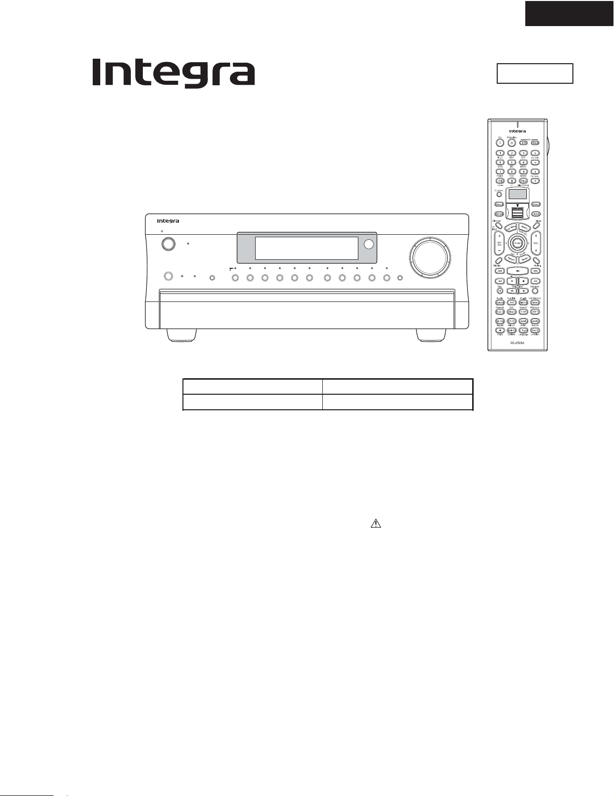
DTR-8.4
SERVICE MANUAL
1
Ref. No. 3788
Standby/On
Direct/
Pure Audio
Pure Audio psamplingU
SERVICE MANUAL
AV RECEIVER
MODEL DTR-8.4
Standby
()
Zone 2
GRN
()
Rec
RED
Audio
Selector
Video 2
Video 1
VCR 2
VCR 1
Video 3 Tape
Video 4 V
DVD
Dec., 2003
Master Volume
ideo 5
Tuner Phono Net AudioCD
Display
Push To Open
DTR-8.4
Black model
BMDD 120V, AC 60Hz
BMPA
230~240V, AC 50Hz
SAFETY-RELATED COMPONENT
WARNING!!
COMPONENTS IDENTIFIED BY MARK ON THE
SCHEMATIC DIAGRAM AND IN THE PARTS LIST ARE
CRITICAL FOR RISK OF FIRE AND ELECTRIC SHOCK.
REPLACE THESE COMPONENTS WITH ONKYO
PARTS WHOSE PART NUMBERS APPEAR AS SHOWN
IN THIS MANUAL.
MAKE LEAKAGE-CURRENT OR RESISTANCE
MEASUREMENTS TO DETERMINE THAT EXPOSED
PARTS ARE ACCEPTABLY INSULATED FROM THE
SUPPLY CIRCUIT BEFORE RETURNING THE
APPLIANCE TO THE CUSTOMER.
Page 2
SPECIFICATIONS
2
DTR-8.4
Amplifier Section
Power output:
All channels:
Dynamic power: 2 x 280 W (3
THD (total harmonic
distortion): 0.08% (rated power)
Damping factor: 60 (8
Input sensitivity and
impedance: 200 mV/50k
Output level and
impedance: 200 mV/470
Phono overload: 120 mV (MM, 1 kHz, 0.5%)
Frequency response: 5 Hz~100 kHz/+1 dB, ~-3 dB (CD, Direct)
Tone control: ±10 dB, 50 Hz (BASS)
S/N ratio (Direct mode): 110 dB (LINE, IHF-A, 0.5 V input)
Speaker impedance: 4~16
110 W (8 , 20 Hz~20 kHz, FTC)
(American Model)
150 W (6
(Australian model)
2 x 220 W (4
2 x 140 W (8
2.5 mV/50k (PHONO MM)
±10 dB, 20,000 Hz (TREBLE)
80 dB (PHONO, IHF-A, 5 mV input)
, 1 kHz, DIN)
, front)
, front)
, front)
)
(LINE)
(REC OUT)
Video Section
Input sensitivity, output
level and impedance: 1.0 Vp-p/75 (component and S-Video
Component video
frequency response: 5 Hz~50 MHz
Y)
0.7 Vp-p/75
0.286 Vp-p/75
1.0 Vp-p/75
(component P
(S-Video C)
(composite)
B/CB, PR/CR)
Tuner Section
FM
Tuning frequency range: 87.5~108.0 MHz
Usable sensitivity: FM STEREO 17.2 dBf, 2.0 µV (75
IHF)
FM MONO 11.2 dBf, 1.0 µV (75 IHF)
S/N ratio: FM STEREO 70 dB (IHF-A)
FM MONO 76 dB (IHF-A)
THD: FM STEREO 0.3%
FM MONO 0.2%
FM stereo separation: 45 dB at 1 kHz, 30 dB at 100 Hz~10 kHz
AM
Tuning frequency range: 530~1710 kHz (American model)
522~1611 kHz (Australian model)
Usable sensitivity: 30 µV
S/N ratio: 40 dB
THD: 0.7%
General
Power supply: American model: AC 120 V, 60 Hz
Power consumption: American model: 9.0 A
Standby power
consumption: 2.5 W
Dimensions
(W x H x D): 17-1/8" x 6-7/8" x 18-1/8"
Weight: 40.8 Ibs. (18.5 kg)
Video Inputs
Component video inputs:2 (Input 1, Input 2)
S-Video inputs: 6 (DVD, Video 1~5)
Video inputs: 6 (DVD, Video 1~5)
Video Outputs
Component video
outputs: 1 (Component Monitor Out)
S-Video outputs: 3 (Video 1 Out, Video 2 Out, Video
Video outputs: 4 (Video 1 Out, Video 2 Out, Video
Audio Inputs
Digital inputs: 8 (Optical 1~4, Optical Video 5 (fixed, on
Analog inputs: 9 (CD, Phono, Tape, DVD, Video 1~4,
Multichannel analog
inputs:
Audio Outputs
Digital outputs: 2 optical
Analog outputs: 4 (Tape Out, Video 1 Out, Video 2 Out,
Pre outs: 8 (Front L/R, Center, Surround L/R,
Subwoofer pre out: 1
Speaker outputs: 7
Phones: 1
Other Sockets
RS-232: 1
IR in/out: 1
12V trigger out: 3
Ethernet (Net-Tune) 1 (10Base-T
Specifications and features are subject to change without
notice.
Australian model: AC 230~240 V, 50 Hz
Australian model: 670 W
(435 x 175 x 460 mm)
Monitor Out)
Monitor Out, Zone 2 Video Out)
front panel), Coaxial 1~3)
Video 5)
7.1 ch (Front L/R, Center, Surround L/R,
Surround Back L/R, Subwoofer)
Zone 2 Out)
Surround Back L/R or Zone 2 L/R,
Subwoofer)
, RJ45)
Page 3

SERVICE PROCEDURES
3
DTR-8.4
1. Replacing the fuses
This symbol located near the fuses indicates
that the fuse used is fast operating type. For continued
protection against fire hazard, replace with same type fuse.
For fuse rating refer to the marking adjacent to the symbol.
Ce symbole indique que le fusible utlise est a
rapide. Pour une protection permanente, n'untiliser que
fusibles de meme type. Ce darnier est la qu le present
symbol est appse.
REF. NO.
F901
F902
F903
F9501,F9502
F9503,F9504
Note:
PART NO.
252196
252078
252244 or
252278
252164 or
252258
252075,
252241 or
252275
252160 or
252254
252075,
252241 or
252275
252158 or
252252
252073,
252239 or
252273
<D>: 120V model only
DESCRIPTION
12A-UL/T-314,Fuse <D>
5A-SE-EAK,
5A-SE-TL250V or
5A-SE-TL250V, Fuse <A>
5A-UL/T-237 or
5A-T/UL-ST2,Fuse <D>
2.5A-SE-EAK,
2.5A-SE-TL250V or
2.5A-SE-TL250V,Fuse <A>
2.5A-UL/T-237 or
2.5A-T/UL-ST2,Fuse <D>
2.5A-SE-EAK,
2.5A-SE-TL250V or
2.5A-SE-TL250V,Fuse <A>
1.6A-UL/T-237 or
1.6A-T/UL-ST2,Fuse <D>
1.6A-SE-EAK,
1.6A-SE-TL250V or
1.6A-SE-TL250V,Fuse <A>
<A>: Australian model only
3. Safety-check out
(U.S.A. model only)
After correcting the original service problem, perform the
following safety check before releasing the set to the customer.
Leakage Current Check
Measure leakage current to a known earth ground(water pipe,
conduit, etc.) by connecting a leakage current tester between
the earth ground and exposed metal parts of the appliance
(input/output terminals, screwheads,metal overlays, etc.).
Plug the power supply cord directly into a 120V AC 60 Hz outlet
and turn Standby switch on. Any current meausred must not
exceed 0.5mA.
4. Memory Preservation
This unit does not require memory preservation batteries.
built-in memory po wer back-up system preserves the contents
of the memory during power failures and even when the unit is
unplugged. The unit must be plugged in order to charge the
back-up system.
The memory preservation period after the unit has been
unplugged varies depending on climate and placement of the
unit. On the average, memory contents are protected over a
period of a few weeks after the last time the unit has been
unplugged. This period is shorter when the unit is e
xposed to a
highly humid climate.
A
2. To initialize the unit
This device employs a microprocessor to perform various
functions and operations. If interference generated by an
external power supply, radio wave, or other electrical source
results in accident which causes the specified operations
and functions to operate abnormally.
To perform a result, please follow the procedure below.
1.Press the STANDBY ON button to turn on the unit.
2.Press and hold down the VIDEO 1 button, then press the
STANDBY/ON button.
3.After "CLEAR" is displayed, the preset memory and each
mode stored in the memory, such as surround, are
initialized and will return to the factory setting.
4.Unplug the power supply cord.
Page 4
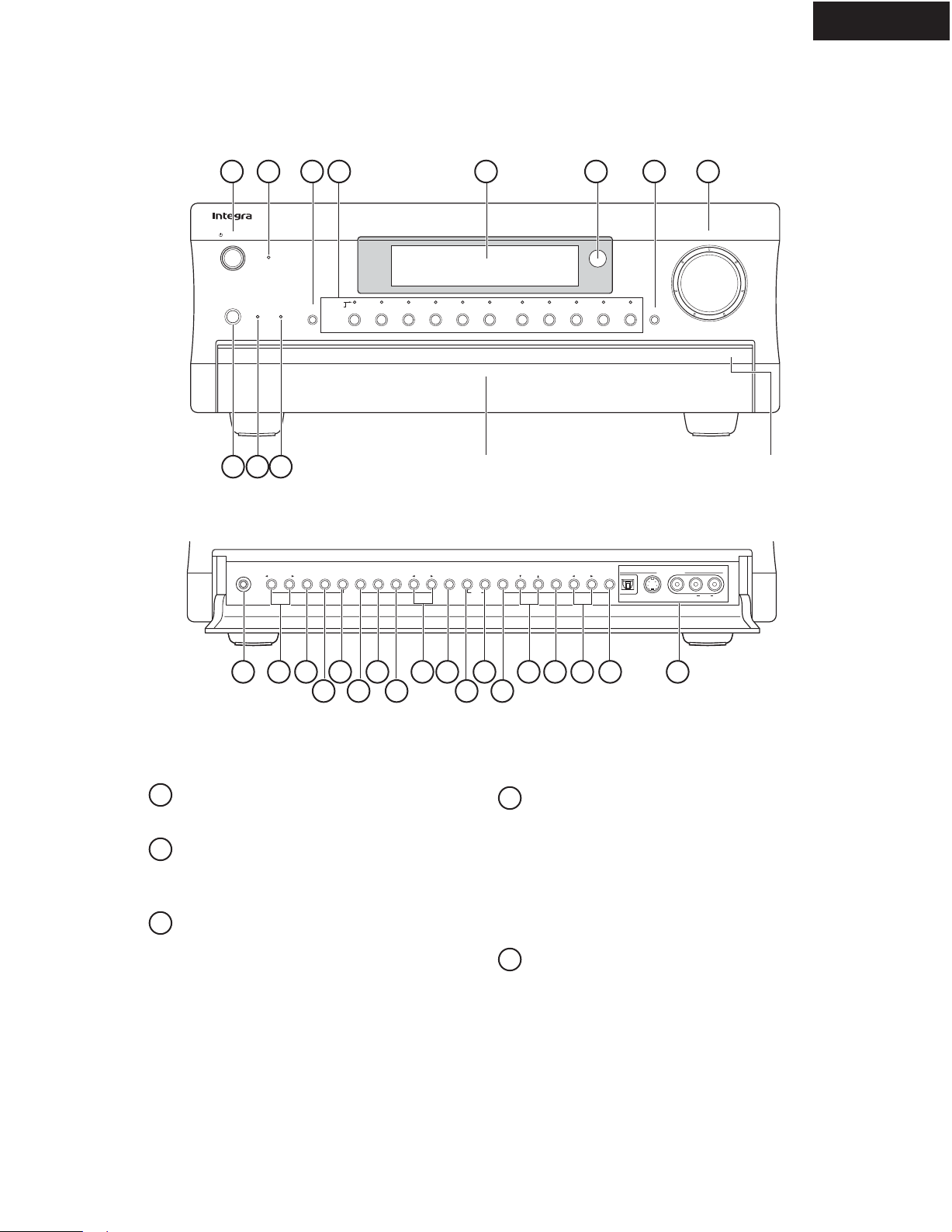
P ANEL VIEWS
4
FRONT PANEL
1 2 3 4 5 6 7 8
DTR-8.4
Standby/On
Standby
Direct/
Pure Audio
Pure Audio psamplingU
9 10 11
Phones
Zone 2
Level
Audio
Selector
()
Zone 2
GRN
()
Rec
RED
DVD
Video 1
VCR 1
Video 3 Tape
Video 2
VCR 2
Video 4 V
ideo 5
Tuner Phono Net AudioCD
Display
Front door Push here to open the flap
Stereo Surround THX
DSPRec Out Zone 2 Off Dimmer Memory
Setup Tuning
FM Mode
Clear
Enter Preset Return
S Video Audio
Digital
12 13 141516 18 20 21 23 25 26 27 28 29
24221917
Video 5
Input
Video L R
Master Volume
Push To Open
DTR-8.4
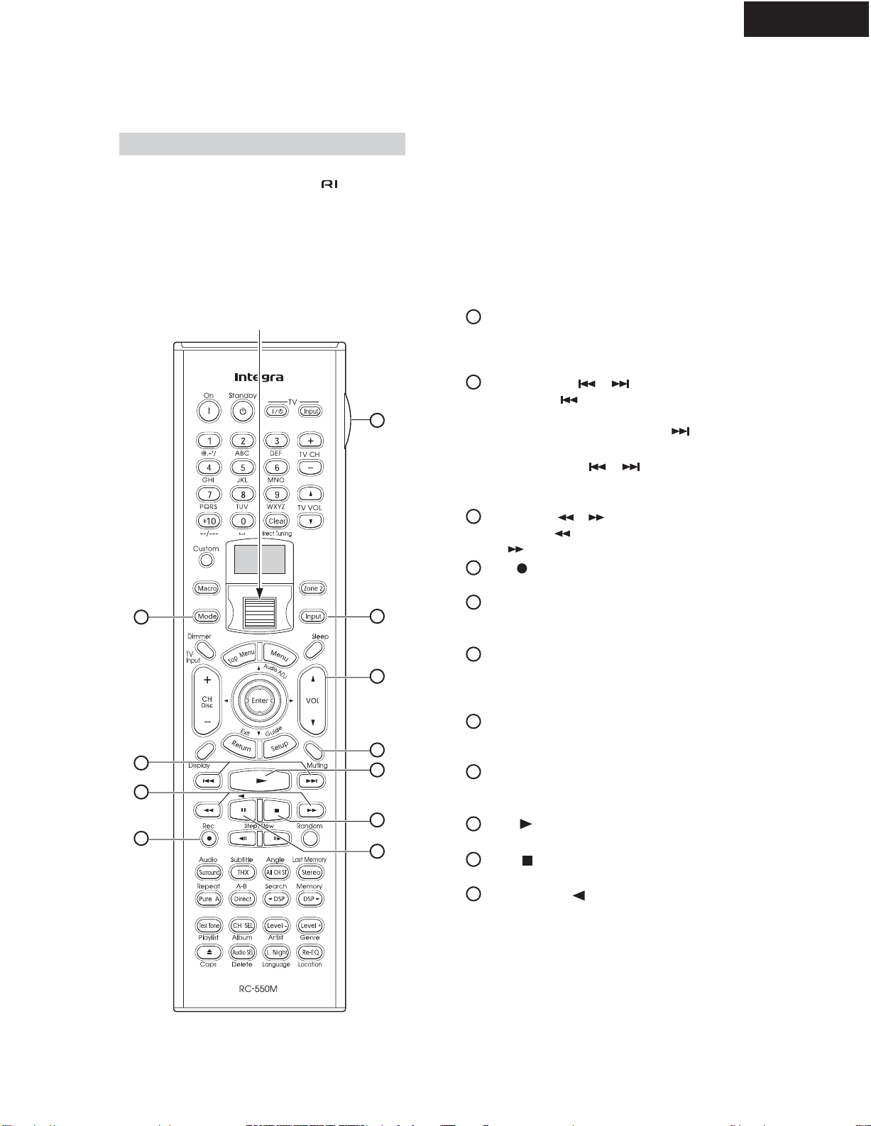
Standby/On button
1
This button is used to set the DTR-8.4 to On or
Standby.
2
Standby indicator
This indicator lights up when the DTR-8.4 is in
Standby mode, and it flashes while a signal is being
received from the remote controller.
Audio Selector button
3
This button is used to select the audio input signal
format: analog, digital, or multichannel.
Input selector buttons & indicators
4
These buttons are used to select the following input
sources: DVD, VIDEO 1~5, TAPE, TUNER,
PHONO, CD, and NET AUDIO. The indicators
show the currently selected input source.
The indicators also show which input source is
selected for Zone 2, in which case they light up
green, or which input source is selected for recording (REC OUT), in which case they light up red.
Display
5
See "Display" on page 3.
Page 5

P ANEL VIEWS
5
FRONT PANEL
DTR-8.4
Remote-control sensor
6
This sensor receives control signals from the remote
controller.
Display button
7
This button is used to display various information
about the currently selected input source.
Master V olume control
8
This control is used to set the volume of the
DTR-8.4 from 0 to 100.
Direct/Pure Audio button
9
This button is used to select the Direct or Pure
Audio listening modes.
Pure Audio indicator
10
This indicator lights up when the Pure Audio listening mode is selected.
Upsampling indicator
11
This indicator lights up when the Upsampling function is on.
Phones jack
12
This 1/4-inch phone jack is for connecting a standard pair of stereo headphones for private listening.
13
Zone 2 Level [ ] [ ] buttons
These buttons are used to set the v olume for Zone 2.
Rec Out button
14
This button is used to select the input source that
you want to record via the REC OUTs (i.e., TAPE
OUT, VIDEO 1 OUT, VIDEO 2 OUT).
15
Zone 2 button
This button is used to select the input source for
Zone 2.
16
Off button
This button is used to turn off the REC OUTs (i.e.,
TAPE OUT, VIDEO 1 OUT, VIDEO 2 OUT) or
Zone 2.
17
Stereo button
This button is used to select the Stereo listening
mode.
18
Surround button
This button is used to select the Dolby and DTS listening modes.
19
THX button
This button is used to select the THX listening
modes.
DSP [ ] [ ] buttons
20
These buttons are used to select the DSP (digital
signal processor) listening modes.
Dimmer button
21
This button is used to adjust the display brightness.
Memory button
22
This button is used when storing and deleting radio
presets.
FM Mode button
23
This button is used to select the FM radio Auto and
Mono modes.
Setup button
24
This button is used to access the onscreen setup
menus (OSD) that appear on the TV .
Tuning [ ] [ ] buttons
25
These buttons are used to tune into radio stations
and to select items on the onscreen setup menus
(OSD).
26
Enter button
This button is used when navigating the onscreen
setup menus (OSD), entering names, and confirming settings.
27
Preset [ ] [ ] buttons
These buttons are used to select radio presets and to
select items on the onscreen setup menus (OSD).
Return button
28
This button is used to return to the previously displayed onscreen setup menu (OSD).
29
Video 5 Inputs
These optical digital audio, S-Video, composite
video, and analog audio inputs can be used to connect a camcorder, g
ames console, and so on.
Page 6
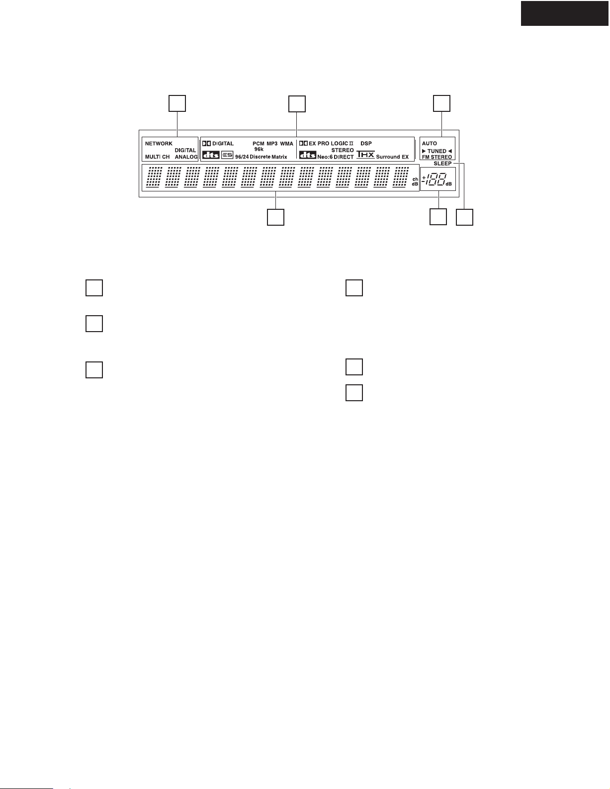
P ANEL VIEWS
6
DISPLAY
DTR-8.4
1
4
Audio input format indicators
1
These indicators show the audio input format for the
currently selected input source.
Listening mode & digital audio format
2
indicators
These indicators show the currently selected listening mode and digital audio format.
3 Tuning indicators
AUTO indicator:
This indicator lights up when the tuner is tuned to
an FM station and Stereo mode is selected. It goes
off when Mono mode is selected.
TUNED indicator:
This indicator lights up when the tuner is tuned into
an AM or FM station.
FM STEREO indicator:
This indicator lights up when the tuner is tuned to a
stereo FM station. It goes off when Mono mode is
selected.
2
3
5 6
Multipurpose display area
4
Normally, the name of the currently selected input
source is displayed here. When you select the AM
or FM input source, the radio frequency and preset
number are displayed. If you press the [Display]
button, the currently selected listening mode and
digital audio format are displayed.
5 Volume level
The volume level is displayed here.
6 SLEEP indicator
This indicator lights up when the Sleep function has
been set.
Page 7
P ANEL VIEWS
7
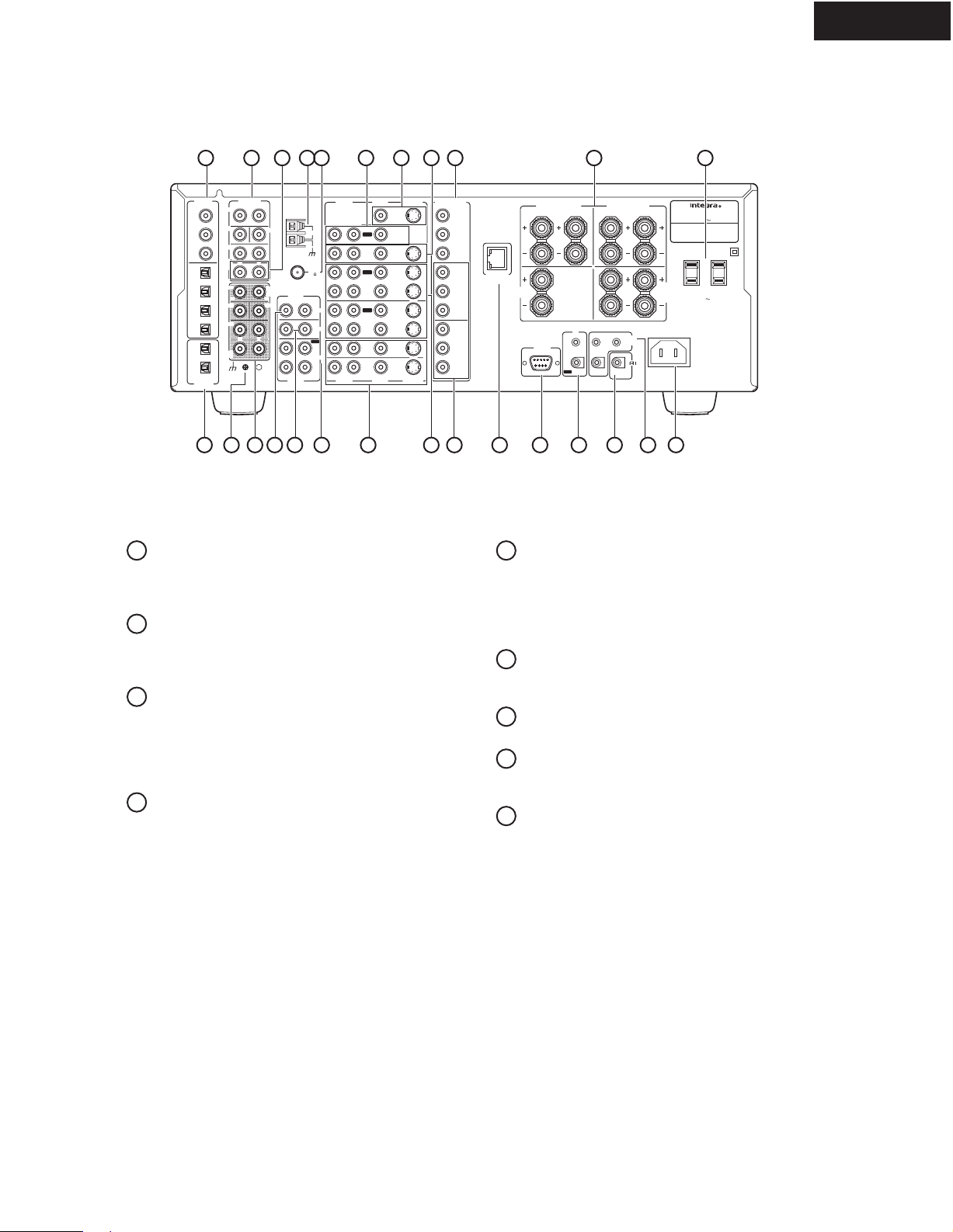
REAR PANEL
DTR-8.4
1
3 456 7
PRE OUT
DIGITAL
IN
FRONT
COAX
1
SUB
2
SURR
3
SURR
BACK/
OPT
ZONE 2
1
FRONT
2
R
SUB
3
SURR
4
OPT
1
SURR
BACK
2
GND
DIGITAL
OUT
26 2422
2
1
DIGITAL IN COAX 1~3, OPT 1~4
ANTENNA
L
R
CENTER
R
L
MULTI CH
INPUT
AUDIO
L
L
R
CENTER
R
L
L
R
AUDIO
8 9
AM
FM
75
PHONO
IN
CD
IN
OUT
TAPE
IN
10
VIDEO
AUDIO
L
R
OUT
IN
OUT
IN
OUT
IN
IN
IN
L
R
VIDEO
AUDIO
These coaxial and optical digital audio inputs can be
used to connect CD, DVD, or LD (laser disc) players and other components with digital audio outputs.
2
DIGITAL OUT OPT 1 & 2
These optical digital audio outputs can be used to
connect a CD recorder or other digital recorder with
digital inputs.
3
PRE OUT- FRONT L/R, SUB, CENTER,
SURR L/R
If you use the DTR-8.4 as a preamp, these analog
audio outputs can be connected to the inputs on a
separate power amp. The SUB output is used to
connect a powered subwoofer.
4
PRE OUT-SURR BACK/ZONE 2
These analog audio outputs can be used to feed the
L/R surround back inputs on a separate power amp
when the DTR-8.4 is used as a preamp, or to feed a
power amp in Zone 2.
1112 13
S VIDEO
MONITOR
OUT
ZONE 2
DVD
VIDEO 1
VIDEO 2
VIDEO 3
VIDEO 4
S VIDEO
1415
16
COMPONENT
VIDEO
OUTPUT
Y
P
PR
INPUT 1
Y
P
PR
INPUT 2
Y
P
PR
17
B
ETHERNET
-Tune)
(Net
B
B
CENTER
SPEAKER
RS232
18 20 21 23
5
MULTI CH INPUT-FR ONT L/R, SUB,
CENTER, SURR L/R, SURR BACK L/R
These analog audio inputs can be used to connect AV
components with multiple analog audio outputs,
including DVD players with individual 5.1/7.1 surround analog audio outputs.
6
AM ANTENNA
These push terminals are for connecting an AM
antenna.
7
FM ANTENNA
This connector is for connecting an FM antenna.
PHONO IN
8
These analog inputs can be used to connect a turntable with a moving-magnet cartridge.
9
CD IN
These analog inputs can be used to connect a CD
player with analog outputs.
19
FRONT SPEAKERS
RL
I R
IN
OUT
R
A
B
SURR SPEAKERS
R
ZONE 2
12 V
TRIGGER OUT
REMOTE
CONTROL
25
SURR
BACK/
ZONE 2
SPEAKERS
L
AC INLET
AV RECEIVER
MODEL NO. DTR
:
RATING
120 V 60 Hz 9.0 A
AC
AC OUTLETS
AC
120 V 60 Hz
SWITCHED
TOTAL 120W 1A MAX.
-
8.4
L
Page 8
P ANEL VIEWS
8
REAR PANEL
DTR-8.4
10
TAPE IN/OUT
These analog inputs and outputs can be used to connect a cassette recorder, Mini Disc recorder, or other
recorder with analog inputs and outputs.
MONITOR OUT
11
This S-Video or composite video output can be connected to the video input on your TV or projector .
ZONE 2 OUT
12
These composite video and analog audio outputs
can be used to feed a TV and an integrated amp in
Zone 2.
DVD IN
13
These S-Video, composite video, and analog audio
inputs can be used to connect a DVD player..
VIDEO 1 & 2 IN/OUT
14
These S-Video, composite video, and analog audio
inputs and outputs can be used to connect one or
two video recorders (e.g., VCRs).
15
VIDEO 3 & 4 IN
These S-Video, composite video, and analog audio
inputs can be used to connect one or two video
sources (e.g., cable TV , satellite TV, or a set-top
box).
COMPONENT VIDEO OUTPUT
16
This component video output can be used to connect a TV or projector with a component video
input.
17
COMPONENT VIDEO INPUT 1 & 2
These component video inputs can be used to connect one or two AV components with component
video outputs, such as a DVD player.
ETHERNET (Net-Tune)
18
This port is for connecting the DTR-8.4 to your
Ethernet network (i.e., router or switch) for use with
Net-Tune (i.e., Internet radio and MP3 and WAV
playback).
SPEAKERS
19
These terminal posts are for connecting your speakers. The SURR BACK/ZONE 2 terminals can be
used with surround back speakers in the main room
or speakers in another room (Zone 2).
RS232
20
This port is for connecting the DTR-8.4 to home
automation and external controllers.
IR IN/OUT
21
If you want to use the remote controller to control
the DTR-8.4 from Zone 2, or if the DTR-8.4 is
installed in a cabinet and the line of sight between
the DTR-8.4 and the remote controller is obstructed,
a commercially available IR receiver can be connected to the IR IN. A commercially available IR
emitter can be connected to the IR OUT to pass the
IR signals along to another AV component.
22
12V TRIGGER OUT ZONE 2/A/B
These outputs can be connected to the 12-volt trigger inputs on other components. They output 12
volts (100 milliamperes max). The ZONE 2 TRIGGER OUT outputs 12 volts while the DTR-8.4 is in
Zone 2 mode. The A and B outputs can be assigned
to input sources, in which case, the assigned trigger
output outputs 12 volts while the input source is
selected.
23
24
25
26
REMOTE CONTROL
This (Remote Interactive) socket can be connected to the socket on another Integra/Onk yo
AV component. The DTR-8.4's remote controller
can then be used to control that component. To use
, you must make an analog RCA/phono audio
connection between the DTR-8.4 and the other
component, even if they are connected digitally.
AC INLET
The supplied power cord should be connected here.
AC OUTLETS
These switched AC outlets can be used to supply
power to other AV components. The connector type
depends on the country in which you purchased
your DTR-8.4.
Grounding screw
This screw is for connecting a turntable's ground
wire.
AV
Page 9
P ANEL VIEWS
9
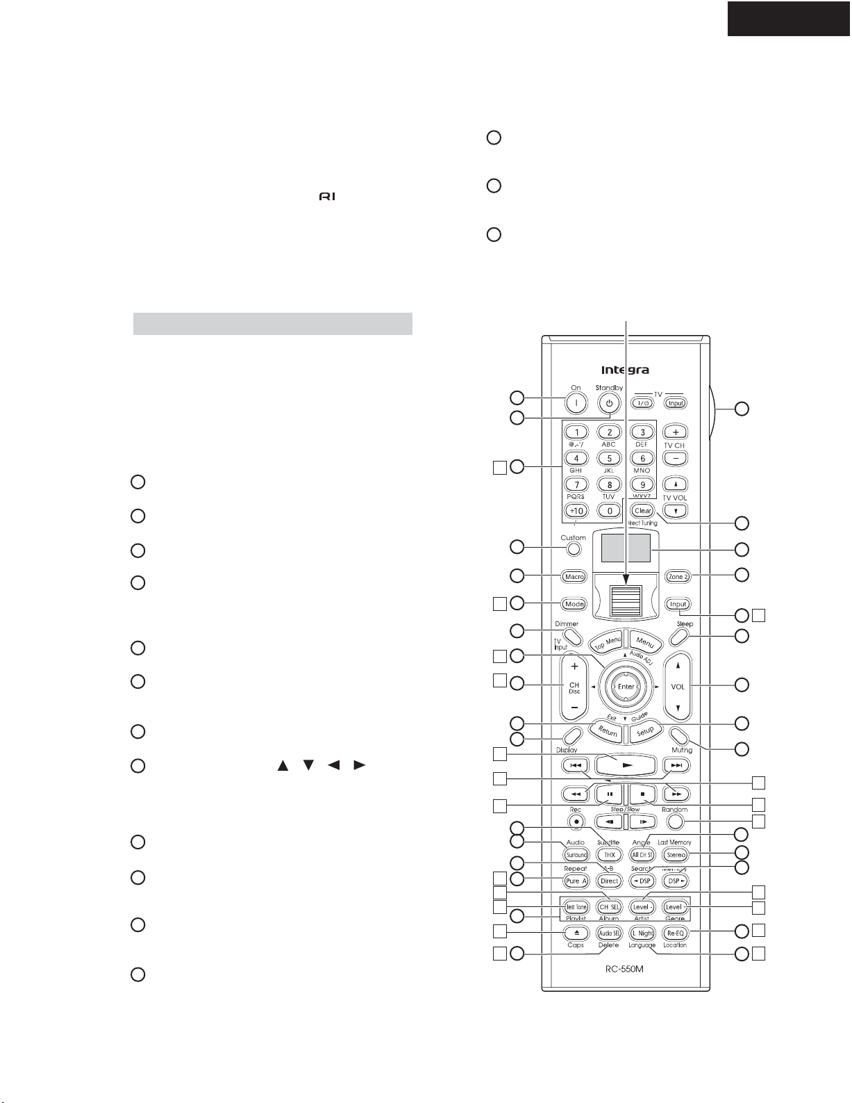
REMOTE CONTROLLER
DTR-8.4
The DTR-8.4's remote controller is a multipurpose
device that can be used to control not just the DTR-8.4
but your other AV components as well. This section
explains how it's various operating modes can be used to
control the DTR-8.4 and various -compatible Integra/Onkyo components.
Amp Mode
Amp mode is used to control the DTR-8.4. To select
Amp mode, press the scroll wheel. "AMP" appears
on the display.
Note:
While neither the [Input] button nor [Mode] button is
illuminated, rolling the scroll wheel changes the input
source and remote controller mode simultaneously.
Boxed numbers are for Net-Tune mode.
1
On button
This button is used to turn on the DTR-8.4.
2
Standby button
This button is used to set the DTR-8.4 to Standby.
Number/letter buttons
3
These buttons are used to enter numbers and letters.
4
Custom button
This button is used to access various settings that
you can use to customize the operation of the
remote controller.
Macro button
5
This button is used with the Macro function.
6
Mode button
This button is used with the scroll wheel to select
the remote controller modes.
Dimmer button
7
This button is used to adjust the display brightness.
Up/Down/Left/Right [ ]/[ ]/[ ]/[ ] &
8
Enter buttons
These buttons are used to select items on the
onscreen setup menus (OSD). The Enter button is
also used to enter names and to confirm settings.
9
CH/Disc button
This button is used to select radio presets.
10
Return/Exit button
This button is used to return to the previously displayed onscreen setup menu (OSD).
11
Display button
This button is used to display various information
about the currently selected input source.
12
THX button
This button is used to select the THX listening
modes.
13
Surround button
This button is used to select the Dolby and DTS listening modes.
14
Direct button
This button is used to select the Direct listening
mode.
15
Pure A button
This button is used to select the Pure Audio listening mode.
Scroll wheel
1
2
3
1
4
5
6
2
7
3
8
4
9
10
11
5
6
7
12
13
14
8
15
9
10
16
11
17
12
18
19
20
21
22
23
24
25
26
27
28
29
30
31
13
14
15
16
17
18
19
20
Page 10
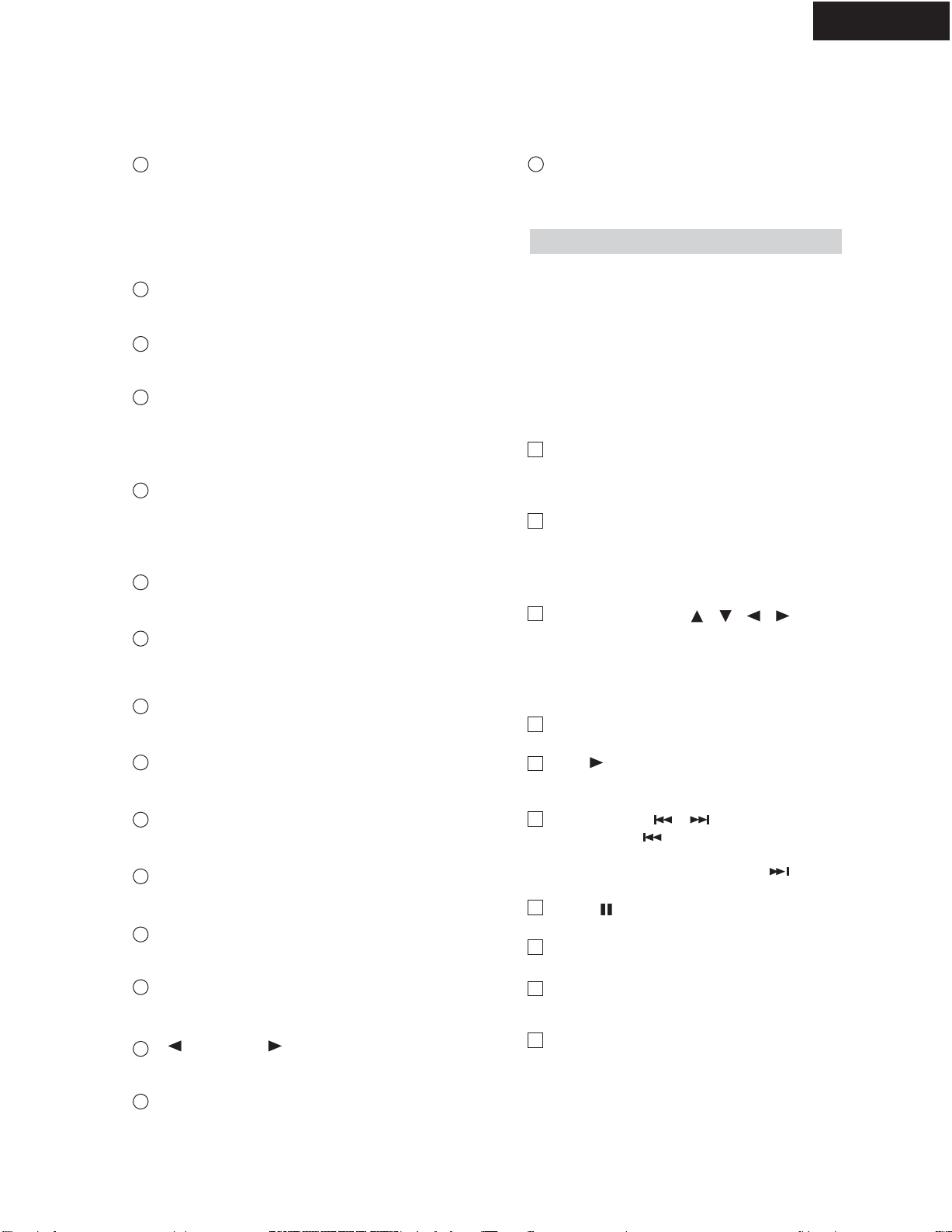
P ANEL VIEWS
10
REMOTE CONTROLLER
DTR-8.4
16
Test Tone, CH SEL, Le vel- & Level+ buttons
These buttons are used to adjust the level of each
speaker individually. These functions can be set
only with the remote controller. The [Leve-] and
[Level+] buttons are also used to adjust the volume
in Zone 2.
17
Audio SEL button
This button is used to select the audio input signal
format: analog, digital, or multichannel.
18
Light button
This button is used to turn on or off the remote controller's illuminated buttons.
19
Direct T uning button
This button is used with the number buttons to
select a radio station by entering its frequency. Press
this button first, and then use the number buttons to
enter the frequency..
20
Display
The top line of this LCD display shows the name of
the currently selected input source. The bottom line
shows the currently selected remote controller.
mode.
Zone 2 button
21
This button is used when you want to set the volume
and input source for Zone 2.
Input button
22
This button is used to select the input source. Press
this button first, and then roll the scroll wheel until
the name of the input source appears on the display.
23
Sleep button
This button is used to set the Sleep function. This
function can be set only with the remote controller.
24
VOL button
This button is used to set the volume of the
DTR-8.4.
25
Setup/guide button
This button is used to access the onscreen setup
menus (OSD) that appear on the TV.
26
Muting button
This button is used to mute the DTR-8.4. This function can be set only with the remote controller.
All CH ST button
27
This button is used to select the All Ch Stereo listening mode.
28
Stereo button
This button is used to select the Stereo listening
mode.
[ DSP] & [DSP ] buttons
29
These buttons are used to select the DSP (digital
signal processor) listening modes.
30
Re-EQ button
This button is used to turn on and off the Re-EQ
function.
31
L Night button
This button is used to set the Late Night function.
Net-Tune Mode
Net-Tune mode is used with the Net-T une functions. To
select Net-Tune mode, press the [Mode] button, and
then roll the scroll wheel until "NET-T" appears on
the display .
Note:
While neither the [Input] button nor [Mode] button is
illuminated, the scroll wheel changes the input source
and remote controller mode simultaneously. (e.g., set the
input source to "MSRV/IRD"and the mode to
"NET-T.")
1
Number/letter buttons
These buttons are used to enter numbers and letters
when searching for music in your network audio
server music library.
2
Mode button
This button is used with the scroll wheel to select
the remote controller modes. Press this button first,
and then roll the scroll wheel until "NET-T"
appears on the display.
3
Up/Down/Left/Right [ ]/[ ]/[ ]/[ ] &
Enter buttons
These buttons are used to navigate Internet radio
and network audio server menus. The Enter button
is used to confirm items and to start playback of
Net-Tune server tracks.
4
CH/Disc button
This button is used to select Internet radio presets.
5
Play [ ] button
This button is used to start playback of network
audio server tracks.
6
Previous/Next [ ]/[ ] buttons
The Previous [ ] button is used to select the previous track. During playback it selects the beginning of the current track. The Next [ ] button is
used to select the next track.
7
Pause [ ] button
This button is used to pause playback.
8
Repeat button
This button is used for repeat playback.
Album button
9
This button is used to search your network audio
server music library by album.
10
Playlist button
This button is used to search your network audio
serv
er library by playlist.
Page 11
P ANEL VIEWS
11
REMOTE CONTROLLER
DTR-8.4
11
Caps button
This button is used to select lowercase letters,
uppercase letters, and numbers when searching for
network audio server music by album, artist, or
playlist.
12
Delete button
This button is used to delete characters entered with
the number/letter buttons.
13
Input button
This button is used to select the input source. Press
this button first, and then roll the scroll wheel until
"MSRV" (network audio server) or "IRD" (Internet
Radio) appears on the display.
14
FR/FF [ ]/[ ] buttons
The FR [ ] button is used to start fast reverse. The
FF [ ] button is used to start fast forward.
Stop [ ] button
15
This button is used to stop playback.
16
Random button
This button is used for random playback.
17
Artist button
This button is used to search your network audio
server music library by artist.
18
Genre button
This button is used to search your network audio
server music library by genre, and to search for
Internet radio stations by genre.
19
Location button
This button is used to search for Internet radio stations by country.
20
Language button
This button is used to search for Internet radio stations by language.
Connecting your -compatible Integra/Onkyo DVD
player, CD player, MiniDisc recorder, or cassette
recorder to the DTR-8.4's socket allows you to control it with the DTR-8.4's remote controller. You only
need to point the remote controller at the DTR-8.4.
T o use the function, you must make an connection and an analog RCA/phono audio connection
between the AV component and your DTR-8.4, even if
they are connected digitally.
DVD Mode
DVD mode is used to control an Integra/Onkyo DVD
player connected to the DTR-8.4 via . To select DVD
mode, press the [Mode] button, and then roll the
scroll wheel until "DVD" appears on the display.
Note:
While neither the [Input] button nor [Mode] button is
illuminated, the scroll wheel changes the input source
and remote controller mode simultaneously (e.g., set the
input source and mode to "DVD".)
On button
1
This button is used to turn on the DVD player.
Standby button
2
This button is used to set the DVD player to
Standby.
3
Number/letter buttons
These buttons are used to enter title, chapter, and
track numbers and to enter times for locating specific points in time.
4
Mode button
This button is used with the scroll wheel to select
the remote controller modes. Press this button first,
and then roll the scroll wheel until "DVD" appears
on the display.
Top Menu button
5
This button is used to select a DVD' s top menu.
Up/Down/Left/Right [ ]/[ ]/[ ]/[ ] &
6
Enter buttons
These buttons are used to navigate DVD menus and
the DVD player's onscreen setup menus. The Enter
b utton is used to start playback of the selected menu
title, chapter, or track and to confirm settings.
CH/Disc button
7
This button is used to select discs on a DVD
changer.
Return/Exit button
8
This button is used to exit the DVD player's
onscreen setup menu and to restart menu playback.
9
Display button
This button is used to display information about the
current disc, title, chapter, or track, including the
elapsed time, remaining time, total time, and so on.
10
Previous/Next [ ]/[ ] buttons
The Previous [ ] button is used to select the previous chapter or track. During playback it selects
the beginning of the current chapter or track. The
Next [ ] button is used to select the next chapter
or track.
11
FR/FF [ ]/[ ] buttons
The FR [ ] button is used to start fast reverse. The
FF [ ] button is used to start fast forward.
12
Pause [ ] button
This button is used to pause DVD playback.
13
Step/Slow [ ]/[ ] buttons
These buttons are used for frame-by-frame playback
and slow-motion playback.
Subtitle button
14
This button is used to select subtitles.
Page 12
P ANEL VIEWS
12
REMOTE CONTROLLER
Scroll wheel
1
2
3
4
5
6
7
8
9
10
11
12
13
14
15
16
17
18
15
Audio button
This button is used to select foreign language
soundtracks and audio formats (e.g., Dolby Digital
or DTS).
16
Repeat button
This button is used to set the repeat playback functions.
A-B button
17
This button is used to set the A-B repeat playback
function.
19
32
20
21
22
23
24
25
26
27
28
29
30
31
18
Open/Close [ ] button
This button is used to open and close the disc tray.
19
Light button
This button is used to turn on or off the remote controller's illuminated buttons.
20
Input button
This button is used to select the input source. Press
this button first, and then roll the scroll wheel until
"DVD" appears on the display.
21
Menu button
This button is used to select a DVD's menu.
22
VOL button
This button is used to set the volume of the
DTR-8.4.
Setup/Guide button
23
This button is used to access the DVD player' s
onscreen setup menus.
24
Muting button
This button is used to mute the DTR-8.4. This function can be set only with the remote controller
25
Play [ ] button
This button is used to start DVD playback.
26
Stop [ ] button
This button is used to stop DVD playback.
27
Random button
This button is used with the random playback function.
Angle button
28
This button is used to select different camera angles.
29
Last Memory button
This button is used with the last memory function,
which allows you to resume DVD playback from
where you left off.
30
Memory button
This button is used with the memory playback function, which allows you to create a custom playlist of
titles, chapters, or tracks.
Search button
31
This button is used to search for titles, chapters,
tracks, and specific points in time.
32
Clear button
This button is used to cancel functions and to clear
entered numbers.
DTR-8.4
.
Page 13
P ANEL VIEWS
13
REMOTE CONTROLLER
CD Mode
CD mode is used to control an Integra/Onkyo CD player
connected to the DTR-8.4 via . T o select CD mode,
press the [Mode] button, and then roll the scroll
wheel until "CD" appears on the display.
Note:
While neither the [Input] button nor [Mode] button is
illuminated, the scroll wheel changes the input source
and remote controller mode simultaneously (e.g., set the
input source and mode to "CD.
Scroll wheel
1
1
2
2
3
3
4
4
5
5
6
6
7
7
8
8
9
9
10
10
DTR-8.4
Boxed numbers are for MiniDisc mode (next page).
On button
1
This button is used to set the CD player to On or
Standby.
2
Number/letter buttons
These buttons are used to enter track numbers and
to enter times for locating specific points in time.
3
")
11
11
19
19
12
12
13
13
14
14
15
15
16
16
17
17
18
18
Mode button
This button is used with the scroll wheel to select
the remote controller modes. Press this button first,
and then roll the scroll wheel until "CD" appears on
the display.
CH/Disc button
4
This button is used to select discs on a CD changer.
5
Display button
This button is used to display information about the
current disc or track, including the elapsed time,
remaining time, total time, and so on.
Previous/Next [ ]/[ ] buttons
6
The Previous [ ] button is used to select the previous track. During playback it selects the beginning of the current track. The Next [ ] button is
used to select the next track.
FR/FF [ ]/[ ] buttons
7
The FR [ ] button is used to start fast reverse. The
FF [ ] button is used to start fast forward.
8
Pause [ ] button
This button is used to pause CD playback.
9
Repeat button
This button is used to set the repeat playback functions.
10
Open/Close [ ] button
This button is used to open and close the disc tray.
11
Light button
This button is used to turn on or off the remote controller's illuminated buttons.
12
Input button
This button is used to select the input source. Press
this button first, and then roll the scroll wheel until
"CD" appears on the display.
13
VOL button
This button is used to set the volume of the
DTR-8.4.
14
Muting button
This button is used to mute the DTR-8.4. This function can be set only with the remote controller..
Play [ ] button
15
This button is used to start CD playback.
16
Stop [ ] button
This button is used to stop CD playback.
Page 14
P ANEL VIEWS
14
REMOTE CONTROLLER
DTR-8.4
Random button
17
This button is used with the random playback function.
18
Memory button
This button is used with the memory playback function, which allows you to create a custom playlist of
tracks.
19
Clear button
This button is used to cancel functions and to clear
entered numbers.
MiniDisc Mode
MiniDisc mode is used to control an Integra/Onkyo
MiniDisc recorder connected to the DTR-8.4 via . To
select MiniDisc mode, press the [Mode] button, and
then roll the scroll wheel until "MD" appears on the
display.
Note:
While neither the [Input] button nor [Mode] button is
illuminated, the scroll wheel changes the input source
and remote controller mode simultaneously (e.g., set the
input source and mode to "MD. ")
1
On button
This button is used to set the MiniDisc recorder to
On or Standby.
2
Number/letter buttons
These buttons are used to enter track numbers and
to enter times for locating specific points in time.
3
Mode button
This button is used with the scroll wheel to select
the remote controller modes. Press this button first,
and then roll the scroll wheel until "MD" appears on
the display.
4
Display button
This button is used to display information about the
current disc or track, including the elapsed time,
remaining time, total time, and so on.
5
Previous/Next [ ]/[ ] buttons
The Previous [ ] button is used to select the previous track. During playback it selects the beginning of the current track. The Next [ ] button is
used to select the next track.
6
FR/FF [ ]/[ ] buttons
The FR [ ] button is used to start fast reverse. The
FF [ ] button is used to start fast forward.
Pause [ ] button
7
This button is used to pause MiniDisc playback.
Rec [ ] button
8
This button is used to start MiniDisc recording.
Repeat button
9
This button is used to set the repeat playback functions.
10
Eject [ ] button
This button is used to set eject the MiniDisc.
11
Light button
This button is used to turn on or off the remote controller's illuminated buttons.
12
Input button
This button is used to select the input source. Press
this button first, and then roll the scroll wheel until
"MD" appears on the display.
13
VOL button
This button is used to set the volume of the
DTR-8.4.
Muting button
14
This button is used to mute the DTR-8.4. This function can be set only with the remote controller.
15
Play [ ] button
This button is used to start MiniDisc playback.
16
Stop [ ] button
This button is used to stop MiniDisc playback.
17
Random button
This button is used with the random playback function.
18
Memory button
This button is used with the memory playback function, which allows you to create a custom playlist of
tracks.
19
Clear button
This button is used to cancel functions and to clear
entered numbers.
Page 15
P ANEL VIEWS
15
REMOTE CONTROLLER
Tape Mode
Tape mode is used to control an Integra/Onkyo cassette
recorder connected to the DTR-8.4 via . To select
Tape mode, press the scroll wheel. "AMP" appears
on the display.
Note:
While neither the [Input] button nor [Mode] button is
illuminated, the scroll wheel changes the input source
and remote controller mode simultaneously (e.g., set the
input source and mode to "TAPE.")
Scroll wheel
1
2
3
4
10
11
DTR-8.4
Mode button
1
This button is used with the scroll wheel to select
the remote controller modes. Press the scroll wheel
until "AMP" appears on the display.
2
Previous/Next [ ]/[ ] buttons
The Previous [ ] button is used to select the pre-
5
6
7
8
9
vious track. During playback it selects the beginning of the current track. The Next [ ] button is
used to select the next track.
The Previous/Next [ ]/[ ] buttons make not
work properly with some cassette tapes depending
on how they were recorded.
3
Rewind/FF [ ]/[ ] buttons
The Rewind [ ] button is used to start rewind. The
FF [ ] button is used to start fast forward.
4
Rec [ ] button
This button is used to start tape recording.
5
Light button
This button is used to turn on or off the remote controller's illuminated buttons.
6
Input button
This button is used to select the input source. Press
this button first, and then roll the scroll wheel until
"TAPE" appears on the display.
VOL button
7
This button is used to set the volume of the
DTR-8.4.
8
Muting button
This button is used to mute the DTR-8.4. This function can be set only with the remote controller.
9
Play [ ] button
This button is used to start tape playback.
10
Stop [ ] button
This button is used to stop tape playback.
11
Reverse Play [ ] button
This button is used to start reverse playback.
Page 16
DTR-8.4
16
A
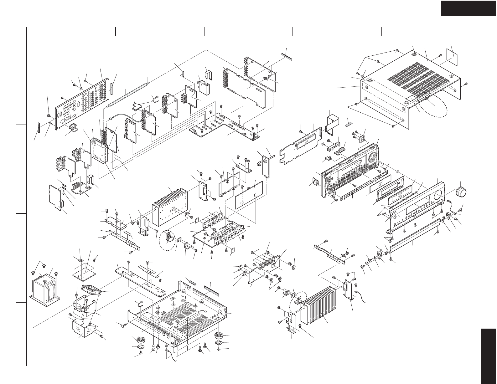
EXPLODED VIEW
1
80
80
15
2
3
77
59
4
85
U35
U31
F901
F902
F903
U27
F6901
F6902
T901
90
94
U8
U30
74
80
U45
U28
21
74
64
89
P2901
61
88
6
74
84
66
61
80
100
47
15
P603C
P602
89
U52
86
91
74
7
108
74
60
17
U55
68
F9501A
95
78
BCDE
80
D
32
104
58
41
43
53
78
98
63
P603
U51
46
96
48
74
61
U42
39
D
U47
87
20
U36
U13
U33
16
99
70
67
P1010
U61
74
5
74
U12
Q6062
Q6052
U21
25
44
74
74
45
U11
U41
U18
U26
99
F9501
F9502
F9504
F9503
Q6066
11
60
17
78
U32
Q6056
U23
U22
82
U7
13
P7701
Q9422B
69
74
U24
19
49
Q9422A
69
U36
U48
67
74
U4
72
14
74
93
72
8
74
73
25
U3
2
U5
62
38
6
74
3
79
78
30
18
37
34
35
1
80
29
40
74
4
80
42
31
12
57
36
80
P7201
U1
U6
51
D
68
39
74
DTR-8.4
Page 17
DTR-8.4
>
>
-
D
17
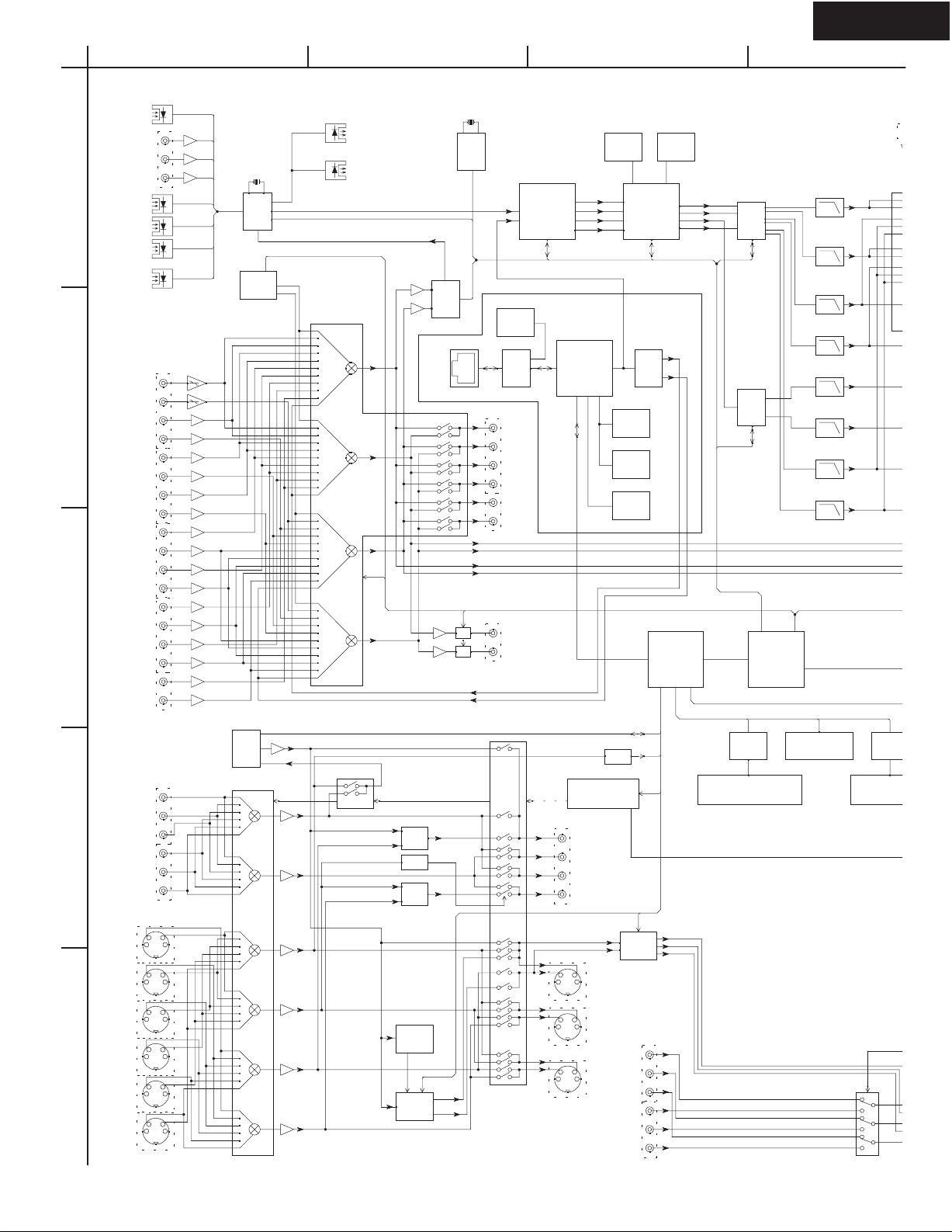
BLOCK DIAGRAM
OPTICAL
VIDEO 5
(FRO
COAXIAL 1
COAXIAL 2
1
COAX
OPTI
OPTI
OPTI
OPTI
AUDIO INPUT
PHONO L
2
VIDEO 1 L
VIDEO 2 L
VIDEO 3 L
3
VIDEO 4 L
VIDEO 5 L
(FRO
IAL 3
CAL 1
CAL 2
CAL 3
CAL 4
TAPE L
DVD L
NT)
CD L
NT)
DIGITAL AUDIO INPUT
R
R
R
R
R
R
R
R
R
A
BCD
RX0
RX1
RX2
76MHZ
24.5
RX3
RX4
RX5
RX6
RX7
DIR
AK4114VQ
FM/AM
TUNER
PACK
DAUX
TX0
DIGITAL AUDIO OUTPU
TC9273F-017
TC9274N-008
RIGHT
REC/
Z2
OPTI CAL 1
CAL 2
OPTI
T
AK4528VF
NETW
ETHERNET
-6dB
-6dB
96/24
2CH A/D
(1/2
ORK
24.5
76MHZ
1M
PROCESSING
MB86 344BPFV
SDRAM
64M
HM52
64165FTT
SDRAM
64M
NM52
64165FTT
4M
MX29
LV320BTC
POST
(THX CINEMA)
R EX)
(SUR
96/24
D/A
WM8716
M30626FGAFP
SRAM
CY7C
1019BV33
SUB MPU
192/24
6CH
AK43
56VQ
96/24
2CH D/A
AK45
28VF
(2/2
D/A
)
M306
MAIN MPU
24FGAFP
50KLPF
VLC
50KLPF
VLC
50KL
50KL
50KL
50KL
50KLPF
VLC
50KL
SL-
C-
SW-
SR
C-
SW-
PF
PF
PF
PF
PF
2ND
TC92
46F
DECORDING
(AC-3,DTS)
(DTS-ES)
(PLI
I,NEO:6)
MB86 D41BPFV
)
MUTE
MUTE
RECOUT
EEPROM 1K
MAC
ADDRESS
93LC 46B
10BASE-T
PHY
CS8900A
L TAPE
R
L VI DEO 1
R
L VI DEO 2
R
ZONE 2/
LINEOUT
L
R
(MP3,WMA DECODE)
Net-Tune
ARM7
MAVE
RICK
EP7312-CV
CY7C
1019BV33
FLASH ROM
COMPOSITE VI DEO INPUT
4
S-VIDEO INPUT
5
VIDE
VIDE
VIDE
VIDE
VIDEO 5
(FRO
DVD
O 1
O 2
O 3
O 4
NT)
VIDEO 1
VIDE
VIDEO 3
VIDEO 4
VIDEO 5
(FRO
OSD
0dB
LC74761
-918
9
DVD
O 2
NT)
YC
YC
YC
YC
YC
YC
REC/
74HC4051
INP
REC/
REC/
COMP
INP
COMP
INP
6dB
6dB
Z2
Y
6dB
Y
6dB
Z2
C
6dB
C
6dB
Z2
RN1444
Y/C mix
RSDET
Y/C mix
MM15 12
GENE
MM10 93
3-LI NE
Y/C
TC90A69F
FSC
RATOR
COMPOSITE VI DEO OUT
RN1444
S-VIDEO OUTP UT
SEP
TC92 73N-004
MONITOR
VIDEO 1
VIDEO 2
ZONE
YC
YC
YC
ISDET
2
MONI
TOR
VIDE
O 1
COMPONENT VI DEO
O 2
VIDE
VIDEO
ENCO
TA12 70BF
1
CB
CR
2
CB
CR
DER
T
INPU
Y
Y
FL D
RIVER
M66004FP
FLT
Key Matrix
Volume Control
LED
DRIVER
Rec Out LE
Zone 2 LED
Page 18
DTR-8.4
18
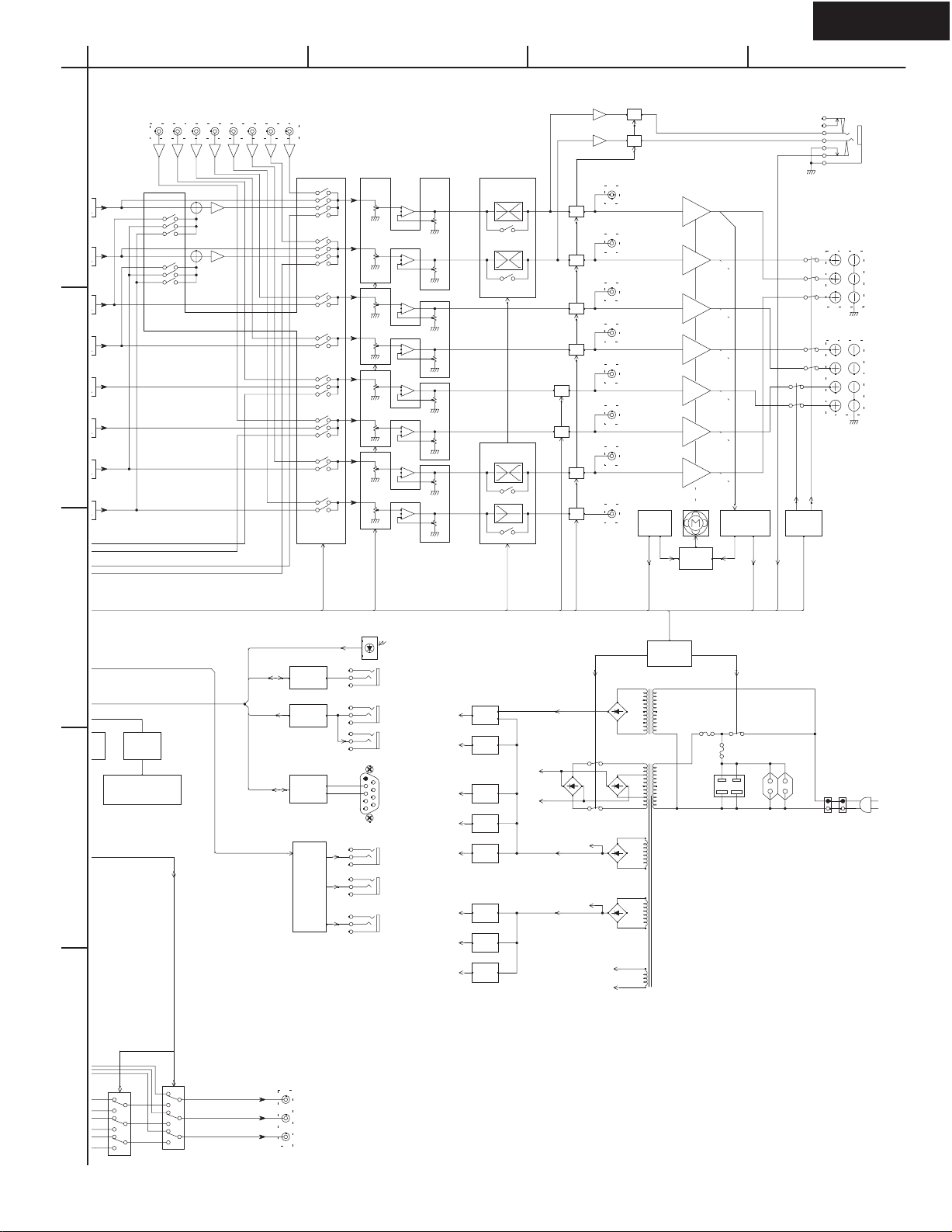
BLOCK DIAGRAM
SBR
1
L
SL->
C->L
SW->
L
R
SR->
C->R
SW->
R
2
A
BCD
11dB
MULTICHANNEL
LRCSWSLSRSBL
INPUT
BYPA
BYPA
BYPA
BYPA
NJU7
NJU7
TONE
306G
MUTE
SS
MUTE
SS
MUTE
MUTE
MUTE
MUTE
306G
MUTE
SS
MUTE
SS
MCL
TL
MCR
MCSL
DSL
MCSR
DSR
MCSB
DSBL
Z2L
MCSB
DSBR
Z2R
MCC
MCSW
DSW
DL
BL
TR
DR
BR
L
R
DC
TC9163
TC9164
-1
-1
MASTER VOLUM E
CUT
TC94A07F
TC94
TC94
TC94A07F
A07F
A07F
BOOS
T
11dB
SUBW
PREOUT
LEFT
RIGH
SURROUND
SURROUND
SURROUND BAC K
SURROUND BAC K
CENT
OOFER
MUTE
MUTE
T
LEFT
RIGH
T
/ ZONE 2 LEF
/ ZONE 2 RIG
ER
THERMAL
SENSOR
PHONE
HEAD
HPEN
Power Amplif ier
+29dB
FRONT SPEAKERS
+29dB
+29dB
+29dB
T
+29dB
HT
+29dB
+29dB
ING FAN
COOL
DRIV
FAN
ER
VOLTAGE SENSOR
CURRENT SENSOR
SURROUND BACK SPEAK ERS
RELAY
DRIV
ER
RIGHT
LEFT
ER
CENT
SURROUND SPEAKERS
RIGHT
LEFT
RIGHT
LEFT
/ZONE2 SPEAKERS
3
RELA
REMOTE SENSO
R
RI
INTE
RFACE
IR
DE-
MODULATOR
LED
DRIVER
RS 232
RFACE
Rec Out LED
Zone 2 LED
INTE
MPD4721GS
4
12V
TRIGGER
ROL
CONT
RI
IRIN
UT
IR O
RS 2
A
12V TRIGGER
B
ZONE 2
+5.6V
STAN
DBY
-27V
-VP
32
AUDI
VIDE
AUDI
VIDE
VIDE
+15V
-15V
+9V
+5V
DSP
+5V
-5V
MAIN AMP
-B1
+B1/
O
O
O
O
O
RELAY
+B2
12V TRIGGER
+B3
FLAC
FL TUBE
FLAC
Y
DRIV
ER
T902
TV-8
FUSE
T901
FUSE
AC O
UTLET
N
AC I
5
COMPONENT VI DEO OUTPUT
Y
CB
CR
Page 19
DTR-8.4
0
F2
66
2
R7340 10K
S
S
O
X
A
19
A
BCD
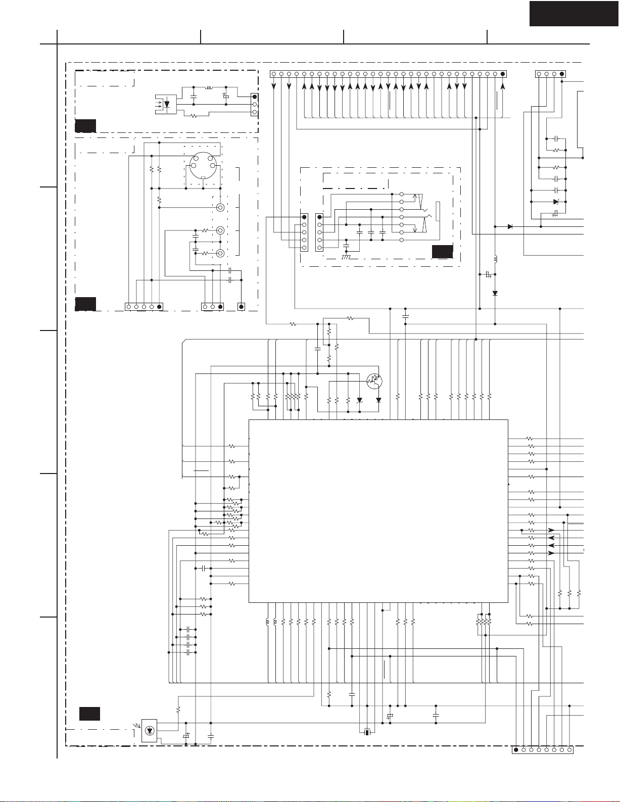
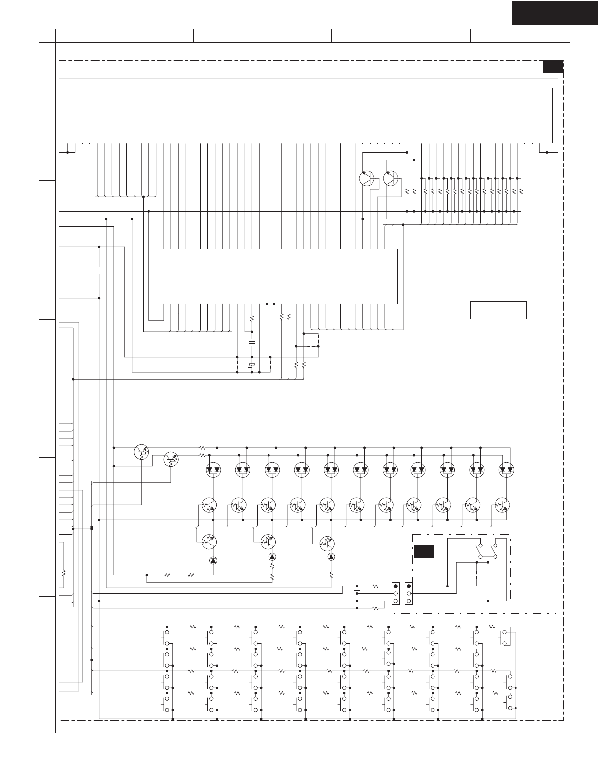
SCHEMATIC DIAGRAM 1 DISPLAY AND SUB MICROPROCESSOR SECTIONS
P7201A (SCH. 9)TO NAAR-80
75
C2572
C2571
RDS
NTSC
MODEL
L2576
NCH-1471
104Z
C2576
R2576
22
R2572
330
471J
330
R2571
471J
P3220B
TO NAAF-7220
(SCH-3)
SYNC
ISS
FLRES
K3
K2
K1
K0
YC
V5-L
V5-R
AGND
10K
R7604
0
R7293
R7294
R7295
R7297
C7206
104Z
R7300 10K
R7397 2.7K
R7395
R7394
C7297
C7295
C7294
C7293
C2579
10/16
10K
R7380
R7282
10K
R7284
10K
R7286
10K
R7386
+5V
DGND
OPT
P2508
S
VIDEO5
IN
V
P2510
L
R
C2577
104Z
C2578
104Z
P2509
1K
10K
R7379
R7280
4.7K
4.7K
4.7K
4.7K
2.7K
2.7K
102K
102K
102K
102K
R7279 1K
P102B
82
84
86
TO NADG-7687 (SCH. 2)
HPDET
MAINREQ
80
P07/D781
P06/D6
P05/D583
P04/D4
P03/D385
P02/D2
P01/D187
P00/D088
P107/AN7/~KI389
P106/AN6/~KI290
P105/AN5/~KI191
P104/AN4/~KI092
P103/AN393
P102/AN294
P101/AN195
AVSS96
P100/AN097
VREF98
AVCC99
P97/~ADTRG /SIN4100
1
LM182
R7201
FLOSDDA
HPR
HPL
HPE
R7382
SUBPOFF
R7377*
AREA2
78
79
2
3
LM182
R7203 1K
R7202
OSDCS
FLOSDCL
GND
RI
VDST
P7482A
1K
C7214102K
R7376*
R7277*
R7276*
RI
4.7K
R7275
AREA1
75
P13/D11 77
P14/D12 76
P16/D14/~INT474P17/D15/~INT5 73
P15/D13/~INT3
78:P12/D10
79:P11/D9
80:P10/D8
1:P96/ANEX1/SOUT4
2:P95/ANEX0/CLK4
3:P94/DA1/TB4IN
4:P93/DA0/TB3IN
5:P92/TB2IN/SOUT3
6:P91/TB1IN/SIN3
7:P90/TB0IN/CLK3
4
5
6
7
1K
1K
1K
1K
R7207
R7206
R7205
R7204
FLCS1
REMIN
DIMPWM
MAININ
ISS
FLOSDCL
SYNC
FLOSDDA
SUBPOFF
MAINREQ
NAETC-7740
P7482B
104Z
C7483
C7484
104Z
R7603
0
10K
R7371
0
R7601
0
R7602
10K
220K
R7272 220
BYTE8
R7301
R7271
71
P20/A0[/D0/_] 72
P21/A1[/D1/D0]
P22/A2[/D2/D1]70P23/A3[/D3/D2]69P24/A4[/D4/D3]68P25/A5[/D5/D4]67P26/A6[/D6/D5]66P27/A7[/D7/D6] 65
SUBMICROPROCESSOR
CNVSS
~RESET
P86/XCOUT11
P87/XCIN10
9
12
1K
1K
1K
R7211
R7209
R7210
R7212 1K
VDCL
VDDA
VDDA
REMIN
C7481
101J
UDZ5.1B
D7202 1SS352
VCC116
XIN15
VDCL
SUBRES
VDST
R7263 1K
63
VSS264
P30/A8[/_/D7]
P84/~INT218
P85/~NMI17
10K
10K
R7218
R7219
SUBRES
HEADPHONES
OSDCS
DIMPWM
C7482
101J
Q7202
RN2403
D7203
Q7201
M30626FHPFP
24:P76/TA3OUT
25:P75/TA2 IN/~W
26:P74/TA2 OUT/W
27:P73/~CT S2/~RTS2/TA1IN/~V
28:P72/CLK 2/TA1OUT/V
29:P71/RXD2/SCL/TA0IN/TB5IN
30:P70/TXD2/SDA/TA0OUT
VSS114
XOUT13
NAETC-7742
U2501
1
TORX178A
U6
NAETC-7741
75
R2575
R2574 75
R2573
2
V5C
GND
V5Y
GND
V-5
U5
3
4
P2506B
TO NAVD-8069
(SCH. 10)
EF
DD PA
R7276 - R7277 - R7289 0 10K
R7290 - 33K
R7291 - R7292 - R7376 10K 10K
R7377 10K 10K
R7389 - 33K
R7390 10K 56K
R7391 10K 10K
R7393
10K
R7389*
R7289*
R7390*
R7290*
R7391*
R7291*
R7392*
R7292*
2.7K
R7392 10K
5
U1
NADIS-7738
U7201
SPS-444-1-
VP
C7207
100/6.3
R7503
330
GND
C7208
104Z
C7213
R7309
10K
X7201
CST16.00MX
102K
W0C1
C7202
100/6.3
VSYNC
232RX
P7481
C7204
474Z
STBY
10K
R7260
VCC262
P31/A9 61
P32/A10 60
51:P43/A19
52:P42/A18
53:P41/A17
P82/~INT020
P83/~INT119
1K
R7220
VSYNC
78
SUBSO
NETTX
NETRX
MAINSO
232TX
U4
RZNET
PURE
UPSPL
RZDVD
10K
10K
10K
R7256 10K
R7255
R7258
R7259
58
P33/A11 59
P34/A12
P35/A13 57
P36/A14 56
P37/A15 55
P50/~WRL/~WR 46
P51/~WRH/~BHE
P57/~RDY/CLKOUT 39
P60/CTS0/RTS0 38
P64/~CTS1/~RTS1/~C 34
P77/TA3IN23
P80/TA4OUT/U22P81/TA4IN/~U21
24
25
26
C7203
474J
GND
MAINSCK
+12V
RZCD
RZPH
RZAM
10K
10K
10K
R7254
R7253
R7252
53
P44/~CS0 50
P45/~CS1 49
P40/A16 54
P46/~CS2 48
P47/~CS3 47
P52/~RD44
P53/BCLK43
P54/~HLDA42
P55/~HOLD41
P56/ALE 40
P61/CLK0 37
P62/RXD036
P63/TXD0 35
P65/CLK1 33
P66/RXD132
P67/TXD1
27
28
10K
220
R7329
R7229
232RX
GND
GND
10K
R7251
52
29
+5.6S
+5.6S
RZT1
51
30
232TX
CNVSS
TO NAPS-7708 (SCH. 7)
SUBREQ
D7502
1SS352
L7201
NCH-1471
C7201
100/6.3
D7201
1SS352
R7250
R7249
R7248
R7247
R7245
45
R7243 10K
R7242
R7240
R7239
R7238
R7237 220
R7236
R7235
R7234
R7233
R7232
R7231
31
R7432
2.2K
4.7K
220
R7431
R7230
R7330
220
CNVSS
RESET
330
RXD1
FLAC1
330
10K
10K
10K
10K
10K
10K
220
220
220
100
100
100
100
CLK1
-VP
C7501
R7501
VDD
FLGND
474Z
220
RTS1
JL72
FLAC2
R7502
C7502
C7509
D7501
C7510
33/50
+12V
LEDGRE
LEDRED
RZV1
RZV5
RZV4
RZV3
RZV2
VBJ
VAJ
SUBR
MAIN
MAIN
SUBS
10K
R7338
NETRX
NETT
GND
TXD1
R7339 10K
P7
FL
Page 20
DTR-8.4
/
R7339 10K
A
20
A
BCD
SCHEMATIC DIAGRAM 1 DISPLAY AND SUB MICROPROCESSOR SECTIONS
7)
L7201A
Q7501
P15
P14
P13
39
40
41
P14
P13
SEG13 47
SEG14 46
SEG15 45
M66005FP
XOUT20
P0
VCC119
18
27K
C7506
474J
16-BT-115GNK
or HNA-16MM40T
P12
P11
P10P9P8P7P6P5P4P3P2
34
35
36
37
38
P9P8P7P6P5P4P3P2P1
P12
P11
P10
SEG08 52
SEG09 51
SEG10 50
SEG11 49
SEG12 48
~RESET13
~CS14
P117
SCK15
SDATA16
1K
1K
R7505
FLOSDDA
1G2G3G4G5G6G7G8G9G
R7506
FLOSDCL
C7508
101J
FLCS1
FLRES
1K
1K
R7507
R7508
NPNPNPNPNP
P1
26
27
28
29
30
31
32
33
Q7503
2SC2712
OR
KTC3875
16G
VCC2 60
SEG01 59
SEG02 58
SEG03 57
SEG04 56
SEG05 55
SEG06 54
SEG07 53
DIG0112
DIG0211
DIG0310
DIG049
DIG058
DIG067
DIG076
DIG085
104Z
C7507
24
25
15G
61
DIG15 62
DIG16
DIG094
DIG103
10G
23
Q7504
14G
DIG14 63
DIG112
11G
13G
12G
NP
16G
15G
14G
13G
12G
11G
10G9G8G7G6G5G4G3G2G1GNPNPF1
14
15
16
17
18
19
20
21
22
10K
10K
10K
10K
R7511 10K
R7512 10K
14G
DIG121 DIG13 64
R7514
R7513
13G
12G
R7516
R7515
11G
10G
10
11
12
13
10K
10K
10K
10K
10K
10K
10K
10K
R7524
R7523
R7522
R7521
R7520
R7519
R7518
R7517
9G8G7G6G5G4G3G2G1G
10K
R7525
NADIS-7738
1
F2F2NPNPP35
502 220
502474Z
509474Z
501 UDZ11B
510
50
V
2
3
P36
P34
P33
P32
P31
P30
P29
P28
P27
P26
P25
P24
P23
P22
P21
P20
P19
P18
P17
P16
42
43
44
45
46
47
48
49
50
51
52
53
54
55
56
57
58
59
60
61
62
63
64
65
66
P36
P35
P34
P33
P32
P31
P30
P29
P28
P27
P26
P25
P24
P23
P22
P21
P20
P19
P18
P17
P16
P15
C7520
104Z
GND
-VP
SEG21 39
SEG22 38
SEG23 37
SEG24 36
SEG25 35
SEG26 34
SEG27 33
VP32
SEG2831
SEG2930
SEG3029
SEG3128
SEG3227
SEG3326
P28
P29
P30
P31
P32
P33
P34
SEG16 44
SEG17 43
SEG18 42
SEG19 41
SEG20 40
Q7502
VSS22
XIN21
SEG3425
SEG3524
SEG3623
P35
P36
R7504
101J
C7504
C7505
C7503
100/6.3
104Z
R7526 10K
U1
F1
123456789
RE
ED
1
V5
V4
V3
V2
BJ
AJ
BREQ
INSCK
INSO
4
BSO
RX
R7340 10K
TTX
5
P7203
FLASH WRITER
OR
LEDRED
K0
K1
K2
PUREAUDIO
K3
Q7536
KTC3875
2SC2712
LEDGRE
S7561
Z2 LEVL<
S7541
STANDBY
/ON
S7542
S7574
FM MODE
OR
Q7537
KTC3875
2SC2712
270
R7536
R7574 330
R7538
R7539
D7521
DVD
PURE
Q7535
D7535
270
R7535
S7562
Z2 LEVL>
S7571
DSP <
S7543
AUDIO SEL
S7552
TUN
S7563
REC
S7572
DSP >
DVD
SML1216C
D7523
V2
RZV2
UPSPL
Q7534
D7534
R7540
R7534
R7563
R7553
RN1402KRC102S OR
D7524V3D7525V4D7526V5D7527T1D7529
V1
Q7524
RZV3
UPSPL
470
470
S7564
ZONE 2
S7573
PTY/TP
DIMMER
S7545
VIDEO 1
S7554
RZV4
STBY
Q7533
D7533
R7564
560R7562 470R7561 330
MEMORY
VIDEO 2
560R7552 470
CD
RZV5
STANDBY
REDGREEN
R7533
470
820 R7565 1.2K
S7565
OFF
S7575
S7546
S7555
NET
C7211
102K
C7212
102K
R7315
R7316
S7566
STEREO
S7576
MENU
S7547
VIDEO 3
S7556
EXIT
RZT1
1K
1K
TU
RZAM
NAETC-7739
U3
P7559B
P7559A
S7567
SURROUND
S7577
TUNING
DOWN
S7548
VIDEO 4
2.2KR7555 1.2KR7554 820
R7556
S7557
PRESET >
D7521-D7532
Q7521-Q7535
180
180
D7522
Q7522 Q7523 Q7525 Q7526 Q7527 Q7529 Q7530 Q7531
RZDVD
RZV1
PURE AUDIO S7569
BLUE
VBJ
VAJ
S7544
S7553
PHONO
D7530
PH
RZPH
D7531CDD7532
VOLUME
R7567 3.9KR7566 2.2K
S7568
THX
R7577
3.9KR7576 2.2KR7575 1.2KR7573 820R7541 330 R7571 470 R7572 560
S7578
TUNING UP
3.9KR7547 2.2KR75461.2KR7545 820R7544 560R7543 470R7542 330
R7548
S7549
VIDEO 5
3.9K
R7557
S7558
PRESET <
RZCD
C7559
104Z
GREEN
NET
Q7532Q7521
RZNET
R7558
12K
DISPLAY
R7551
S7551
TAPE
R7578
12K
S7579
ENTER
RED
C7569
S7559
12K
104Z
Page 21
DTR-8.4
A
C
C
C
C
D
D
D
S
LRCKI236
C
C
N
S
D
D
P
D
D
VDDI5 73
V
S
X
104Z
CKO10
XI7
N
D
P
C
XTI
21
A
BCD
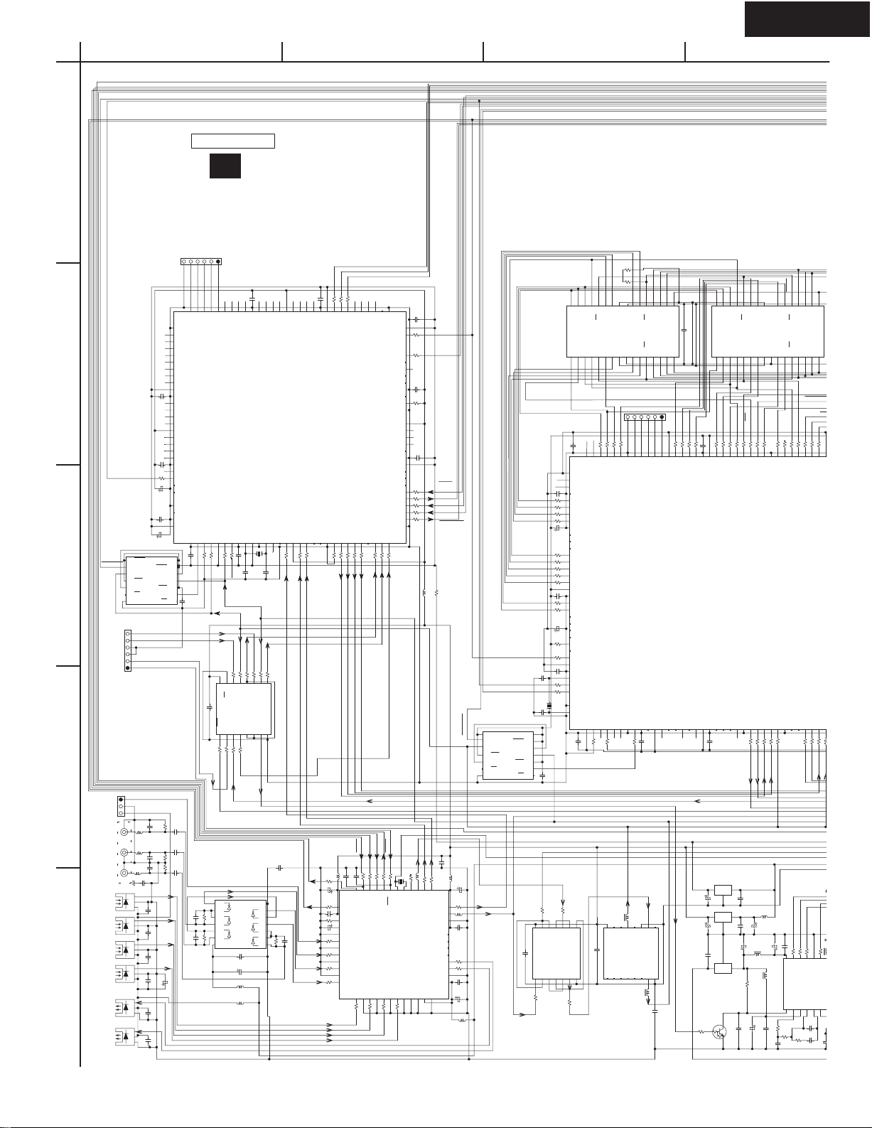
SCHEMATIC DIAGRAM 2 DSP and Main microprocessor sections
NADG-7687
1
2
C709
104Z
104Z
C710
R743
1K
DSPPM"
C720
4
100/
C711
104Z
C719
4
100/
141CLR1
(SCH.8)
P603B
1D2
1CK3
4
1PR
1Q5
6
1Q
GND7
BCKEX2
LRCK EX2
GND
SDIEX2
+5VDAC
Q701
TC74VHC74FT
2CLR
VCC
2D 12
2CK11
2PR
2Q 9
SN74AHC74
2Q
13
10
8
DSP1RST"
3
FROM NADG-7662
4
P100
OPTVCC
FROM
FRONT
(SCH.1)
P101
COAXIAL1
COAXIAL2
IAL3
COAX
TORX179
U100
OPT1
U101 TORX179
OPT2
U102 TORX179
OPT3
U103 TORX 179
5
OPT4
U104
TOTX
179
U105
TOTX
75
104K
R130
101J
C130
R133
C134
LM182-T
LM182-T
C135
R134
104K
R131
101J
C131
75
C136
R135
R132
C132
101J
75
LM182-T
104K
C133
104Z
104Z
C142
C143
104Z
104Z
C144
104Z
C145
47/6.3
C146
104Z
C147
104Z
179
C148
P701
VSS1191
A892
A793
A694
A595
A496
A397
D798
D699
VDDI5100
VSS12101
D5102
D4103
D3104
D2105
VDDE3106
D1107
D0108
A2109
A1110
VSS13111
A0112
PM113
SDI3114
SDI4115
SYNC116
TST2/VSS117
GP11/VSS118
C700
C712
OPTO
GNDDAC
U7
DSP1GP8"
A13 66
A14 65
A15 64
TST1 /BTACT 55
GP13/CLKEN
GP12/SDCLK
SDO325
SDO4
SPDIF27
26
DSP1 2SD4
DIRCS
DSPCL
1K
R1521KR153
INT036
OCKS0/CSN/CAD0 35
IPS0/RX4
NC02
1
470
R139
61
63
A16
A17 62
VDDI3 60
EXLOCK 59
MOD058
MOD1 57
BST56
BOOT54
PAGE 0 53
PAGE1 5
VSS751
PAGE2 50
WMD049
VSS648
WMD147
VDDE146
WE0 45
CS044
DQM/OE0 43
GP15/CAS 42
VSS541
VDDI2 40
GP/1 4RAS 39
HCS36
HDOUT 35
HCLK34
HDIN 33
HACN32
VSS431
LRCKI228
BCKI 229
30
R715
R713
330
330
330
2
SDI2
BCKI
LRCKI2
SDI2
CDTO
DIRPD
DSPDA
1K
1K
220
R150
R149
R151
33
CM1/CSN/SDA
CM0/CDTO/CAD132
OCKS0/CCLK/SCL34
AK4114VQ
TEST24
DIF0/RX53
DIF1/RX65
470
R141
R140
DSP1GP9"
DSP1GP10"
VSS8
38
37
SDI2
XTL-24.57M
31
XTI 30
PDN
Q131
DIR
DIF2/RX77
NC16
470
XTI
X130
2
R142
BK16
29
XTO
IPS1 /IIC8
C706
104Z
R730
R727
C705
104Z
R725
1K
C704
104Z
R720
R719
R718
R717
R716
08LM182
47
DAUX 28
P/SN9
L134
R148
MCK2
MCKO2 27
XTL010
1K
330
1K
330
1K
1K
330
022M
+3.3V
DALRCK
DIRBCK
47
R147
BICK 26
MCKO123
DVDD21
VOUT 20
UOUT19
COUT18
BOUT 17
XTL111
TDI
TCK
TMS
TDO
XRST
DSP1
TDI90
TCK89
XTRST 88
DSP1
104Z
C708
DSP1
87
A9 82
A10 85
A11 84
A12 83
TDO 86
TMS
VSS1 0 81
VDDE2 76
D8/GP0 80
D10/GP278
D11/GP377
D9/G P1 79
330
330
330
R734
R733
R732
C707
104Z
GP869
GP968
VSS971
GP1067
VDDI 4 70
D12/GP475
D13/GP574
D14/GP6 73
D15/GP772
Q700
MB86D41PFV-G-BND
DD/DTS/AAC-DECODER
TST3
119
/VSS
VDDI6
120
VSS01
080D
080D
C137
C138
MCLK212
MS13
VDD110
VSS211
MCLK19
LRCKI3/FS2
EXTI N3
PLOCK7
VDDI05
VSS18
BCKI3/FS1
XRST
2
6
4
R702
R700
R701
R703
C701
104Z
104Z
1K
16
VCC
SEL
1
R190
EX2
8
9
10
11
12
13
330
330
DACBCK
LRCKEX2
330
R198
R199
15
ST
4A14
Q190
TC74 HC157
SN74AHC157
1A2
1B3
R193
R192
R191
330
330
ADDA
SDIEX2
Q130
VCC14
104Z
C140
47/6
C141
L130
470K
L136
470K
X700
C703
220J
C702
220J
XTL-13.5M
DALRCK
LRCKI2
BCKEX2
DACBCK
BCKI2
47
330
330
47
330
R196
R195
R194
R197
4B13
4Y12
3A 11
3B 10
3Y 9
1Y4
2A5
2B6
2Y7
GND8
47
LRCLPLL
SDI2
C179
104Z
GND7
6
5
4
74HC U04
3
2
1
R138
.3
104Z
330
330
DALRCK
104Z
+3.3V
C190
10K
R136
R137
10K
UT
BCKO20
LRCKO19
VDDE016
BCKI117
R706
R707
330
330
DIRD A
DIRBCK
INT1"
104Z
R156
OPTF
RONT
COAX
IAL1
COAXIAL2
KFSO22
SDI118
SDO123
SDO224
VSS321
R708
R71147R71247R714
R710
R709
47
47
330
DSP1 2SD1
DSP1 2SD2
DSP1 2SD3
LRCKI2
+3.3V
022M
102K
101J
R154
220
L135
C155
C156
INT0"
C157
47/4
INT1
R155
220
37
C158
AVDD38
18K
R39
/50
C1590.47
VCOM
40
AVSS541
R157
RX042
470
NC4
43
R158
RX144
470
TEST145
R159
RX246
470
NC547
R160
RX348
470
470
OPT1
OPT2
OPT3
OPT4
+5VD
SP
LRCKI115
SCKOUT14
R705
330
DIRL RCK
080D
C139
10K
COAXIAL3
HDOUT"
DSPC L"
DSPD A"
L701
L702
+2.85V
DIRDA
47
R146
25
LRCK
DVSS22
TX1
TX0 15
NC214
TVDD13
VIN12
GNDD
INT1"
DSP1
BST"
DSP1
HCS"
DSP1
0.82
+5VD AC
C129
SDTO
24
16
HACN"
104Z
022M
47/6.3
R145
L132
104Z
C151
R144
R143 47
104Z
C149
10/16
C150
AC
022M
C152
L131
+3.3V
L133
47
DSP2RST"
INT1"
DSPPM"
DSPPM"
DSP2
1D2
1CK3
4
1PR
1Q5
1Q
6
GND7
DIRLRCK
MCK1
BK16
08LM182
47
OPT
OUT
BST"
Q751
TC74VHC74FT
C769
220J
120J
C770
VCC
2CLR
2D 12
2CK 11
2PR
SN74AHC541
2Q 9
2Q
A2
A1
D6
D5
OE0
A0
D4
D3
D2
D1
D0
INT1"
XTL-13.5M
141CLR1
13
10
8
104Z
C128
R175
104Z
56
56
56
56
56
56
56
56
56
104Z
56
56
4.7K
1K
1K
C761
R173
14
VCC
1A1
330
MCK1
C760
R790
R790
R790
R790
C764
4
100/
R791
R791
R791
R791
R792
C767
R793
R794
C765
100/
4
R795
R796
C768
104Z
R797
1K
R798
X751
DACBCK
104Z
UPSMPL
10K
R174
4A 13
4B 12
4Y 11
Q121
TC74VHCT00
1B2
1Y3
2A4
A3A2A1
A1415
A1514
CY7C 1019BV33 -15VCT
Q705
A1019
A1118
A1217 A1316
A4A5A6A7A8D7D6
104Z
C759
108
GP9
109
7
VDDI
GP8110
GP7111
GP6112
A2113
A1114
D6115
D5116
VSS11117
GP5
118
119
GP4
GP3
120
OE0121
A0122
D4123
D3124
D2125
VDDE4126
VSS12127
D1128
D0129
GP2130
GP1131
GP0132
NC3133
BTSL134
NC4135
EXLOCK136
VDDI8137
VSS13138
MCLK2139
PM140
BST141
BOOT142
VSS1 4143
144
MCLK1
VDDI11
104Z
C751
MCK2
330
3A 10
3B 9
3Y 8
GND7
2B5
2Y6
330
R126
A0
R745
330
A1613
A920
GP10 107
EXTIN2
+3.3V
104Z
C122
R7102
10K
10
3
R710
D1
D0
A13
A14
A15
WE0
12
WE
A821
A3A4D7
A3 106
D3
D2
I/O3 10
I/O4 11I/O522
I/O623
R78956R78956R78956R789
A4 105
D7 104
D8
56
GND19
VCC2
24
D8 103
VCC18
GND225
VSS10 102
A16
5OE28
CS
A0 4
A1 3
A2 2
A3 1A432
I/O1 6
I/O2 7
I/O726
I/O827
D5
D4
P750
D2TMS
DSXRST
101
TMS 100
104Z
C762
A729
A531
A630
A9
A10
A11
A12
OE0
D9
D10
A5
56
D2TDO
D2TD I
D2TCK
A5 95
D9 94
TDI 98
TDO99
D10 93
VDDI6 96
Q703
MB86344BPFV-G-BND
THX/OOS/BASS-MANAGEMENT
MOD06
WMD13
R747
1K
MOD15
WMD04
DACBCK
R124
14
15
Q10
Q11
VDD16
Q120
TC74VHC4040
Q121
VSS07
DALRCK
3
Q74Q 8 1
XRST8 XTRST
R750
C752
1K
LRCLPLL
MCK1
DALRCK
+5VDAC
+2.85V
UPSMPL
+5VD SP
08LL241
BK16
Q9 12
08LL241
BK16
VSS19
ADDA
EX2
RSET11
R125
C160
PAGE015
SCKOUT10
SYNC12 TCK97
VDDI211
PAGE114PAGE213PLOCK16
104Z
XTI
GND
9
Q1
CL_10
Q2
VSS
7Q36Q45Q53Q62
8
DACBCK
104Z
LRCL
PLL
A3A2A1
A0
D8
WE0
12
WE
A1415
A1514
A1613
I/O4 11I/O522
CY7C1019BV33 -15VCT
Q706
A821
A920
A1019
A1118
A1217 A1316
A4A5A6A7A8
D12
WE0
CS0
A6
D11
D12
D13
D14
56
56
56
56
R787
R786
R78756R78756R787
R78856R78856R78856R788
C758
D11 92
VSS9 91
BTACT17
VDDE118
+2.85V +5VD SP
4
100/
Q171
+3.3V
100/4
104Z
+15V
KRC104S
RN14
Q162
R169
47
GNDDAC
104Z
D12 89
VDDE3 90
VSS219
D3120
C753
104Z
Q170
MPC29285T
O
G
C177
MPC2933T
O
G
C178
C171
G
I
Q161
78L0 5
04
R785
A6 86
CS084
D13 88
D14 87
WE0 85
A1723
D3021
SDO325
VSS324
D2922
R755
47
DACDA4
I
C174
104Z
NCH-1479
I
104Z
C176
C175
.3
L162
C172
47/6
470K
O
1.5K
R161
C163
470J
C167
R784
R756
RAMCE
D9
GND19
I/O3 10
VCC18
GND225
I/O623
VCC2
24
D13
1K
220
R783
HACN 83
VSS8 81
HDOUT 82
SDI127
SDI228
SDO426
R757
R759
R758
47
330
330
DACDA3
DSP12SD2
DSP12SD1
L170
470K
.3
47/6
.3
C170
47/6
L160
470K
.3
R162
C168
104Z
47/6
470J
C164
A16
D10
D11
A13
A14
A15
5OE28
CS
A0 4
A1 3
A2 2
A3 1A432
I/O1 6
I/O2 7
A729
A531
A630
I/O726
I/O827
OE0A9A10
A11
A12
D14
D15
DSP2HAC
DSP2H
DS
A7
A8
DSP
D15
DS
1K
1K
56
56
R779
R782
R7801KR781
R78256R78256R782
A7 78
A8 77
HCS 76
D15 80
D16 79
HDIN 74
HCLK 75
V
VD
B
LR
KF
S
S
V
VD
S
B
LR
B
B
A1534
A1633
D2732
LRCKI129
SDI335
VSS430
D28
31
330
R76056R761
R763
R762
56
A16
A15
DALRCK
C169
R163
5.6K
DALRCK
DSP12SD3
104Z
DSPD A
2NDPLLCL
2NDPLLCS
2NDPLLLOCK
1K
1K
10K
R165
R166
R1671KR168
M1 11
M2 12
S1 13
S2 14
VDD16
LOCK15
Q160
TC92
46F
AMPI4
AMPO5
PD2
REF1
VDDA3
VSSA6
102J
C165
1.5K
C166
R164
C161150J
100
474K
Page 22
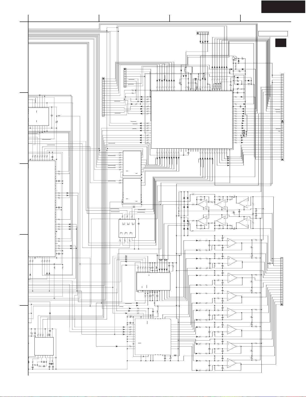
DTR-8.4
HDOUT 82
SDI127
7
7
47/6
3
R758
330
V
GND19
VCC224
22
A
DSPDA
DSPC L
1
XPOR SUBP OFF/FCL
XDAC
S SUBRST/FDI
XDARST CVSS
DSPD
A WRESET
NPOWER
DSPCL
SCL
SDA
SUBPOFF/FCL
MAINREQ
RAMCE
A16
D10
D11
A13
A14
A15
A0 4
A1 3
A2 2
A3 1A432
CS5OE28
I/O1 6
I/O2 7I/O726
VCC18
33 -15VCT
A729
I/O827
GND225
2
OE0A9A10
D14
D15
DSP2HACN"
A7
A8
D15
1K
56
56
R782
R78256R78256R782
79
A7 78
A8 77
D15 80
D16
VSS8 81
3
ENT
D2732
LRCKI129
SDI228
D2831
VSS430
330
R759
R760
56
4
5
A16
DALRCK
DSP12SD2
9
0
0K
104Z
2NDPLLCL
2NDPLLLOCK
.
1K
C169
C170
R1671KR168
S2 14
VDD16
LOCK15
Q160
470K
TC92
PD2
REF1
VDDA3
1.5K
R162
C168
R163
R164
5.6K
100
470J
C164
L753
+3.3V VLSTB
VCCMEM2
C763
104Z
470K
A531
A630
C766
100/4
A11
A12
DSP2
HDOUT"
DSP2HCS" UPSMPL
DSPCL" DSPC L
DSPD A" DSPD A
1K
R779
R7801KR781
C757
104Z
N.C2
72
HCS 76
HDIN 74
HCLK 75
VDDI5 73
71
N.C1
R778
56
A9
R777
56
A10
67
C756
104Z
47
47
56
56
DACBCK
DALRCK
DACBCK
56
56
DSP12SD4
DACBCK
0.82
L752
+2.85V
DACD
A1
DACD
A2
A11
A12
A13
A14
R775
R774
R773
58
57
56
C755
104Z
53
52
51
R772
R771
330
8
R770
1K
R769
330
44
43
R768
R767
330
40
R765
R764
38
330
37
C754
104Z
330
330
L751
022M
150J
C173
08LM182
L161
BK16
VSS 9
XO
8
680
R176
XTL-24.576M
120J
C162
DSPD A
1K
R166
102J
C165
C166
474K
A1633
R761
56
S1 13
46F
AMPI4
LRCKI3 47
A1534
R762
A15
M2 12
AMPO5
A9 70
A10 69
D17 68
D18
VSS7 66
VDDI4 65
BCKO 64
LRCKO 63
KFSI O 62
SDO2 61
SDO1 60
A11 59
D19
D20
D21
VSS6 55
VDDE2 54
D22
D23
D24
A12 50
SPDIF 49
BCKI3 4
BCKI2 46
VSS545
D25
D26
A1342
A14 41
MS
SDI439
BCKI1
VDDI3
LRCKI236
SDI335
R763
DALRCK
DSP12SD3
XTI
2NDPLLCS
10K
R165
M1 11
CKO10
VSSA6
XI7
150J
C161
X160
SUBRST/FDI
TO NAAR-8078(SCH.9)
NET
SUBSO
MAIN SO
MAINCL
2
SUBREQ
P700
CODECPD SPRL Z2
R7126
330
DSPDA"
R7128
330
DSPCL"
DSP1RST"
R715
M"
DSPP
R715
DSP1GP8"
R715
DSP1BST"
R715
HCS"
DSP1
R715
DSP2RST"
R7153~R7158:
330
R7159
DSP2
BST"
R7160
DSP2HCS"
DSP1HDOUT"
DSP2
HACN"
HACN"
DSP1
INT1" INT1
INT0" INT0
DSP2HDOUT"
DACDA2 RDACDA3 SL+
DACDA4 SLDALRCK SR+
BCD
(SCH.7)
AIN AMP
TO M
P7701A
VOLH
SEC1H
SCHEMATIC DIAGRAM 2
PRTCTV
PRTCTHM
DSP and Main microprocessor
sections
CSTC
PRTCTV
V16.0MXJ
SEC1H
0C
PRTCTHM
Z2MUT
AMUT
1K
P86/XCOUT11
P22/A2[/D2/D1]70
1K
DSP1HACN
4
4.7K
R7010
R70711KR70721KR7073
4.7K
R827
1.2K
1.2K
R828
R831
2.2K
R832
R833
2.2K
2.2K
R834
R835
1.2K
1.2K
R836
R837
1.2K
1.2K
R838
R839
2.2K
2.2K
R840
R841
1.2K
1.2K
R842
22K
R7110
CVSS
1K
2.2K
R7009
S9
CNVS
P87/XCIN 10
80:P10/D8
79:P11/D9
78:P12/D10
P20/A0[/D0/_]72
P21/A1[/D1/D0]71
DSP2 HACN
DSP2 HDOUT
6
5
3
2
C819
R829
1.2K
1.2K
R830
2.2K
C823
C824
C825
C826
HPMUT
470
470
470
R7007
R7006
R7005
10K
1K
7
R7109
R710
6
7
BYTE 8
P97/~ADTRG/SIN4100
P104/AN4/~KI0 92
P105/AN5/~KI1 91
P106/AN6/~KI2 90
P107/AN7/~KI3 89
P17/D15/~INT573
P16/D14/~INT474
P15/D13/~INT375
R7075
1K
1K
330
INT1
INT0
TNCS2
101J
4.7K
R108
C104
7
NJM4580M-D
NJM4580M-D
1
101J
4.7K
C105
R109
4.7K
R843
R859
472J
R860
R844
4.7K
R845
4.7K
R861
R862
C820
472J
4.7K
R846
4.7K
R847
180
R863
R864
R848
4.7K
R849
4.7K
R865
R866
180
4.7K
R850
4.7K
R851
R867
R868
472J
R852
4.7K
R853
4.7K
R869
R870
472J
180
4.7K
R854
4.7K
R855
180
R871
R872
472J
R856
4.7K
R857
4.7K
R873
R874
333J
4.7K
R858
GND
FLAS HDO
P7000FLASH WRITER
FLAS HBY
VCCP UP
10K
R7132
R7131
10K
R7031
1K
R7032
1K
R7033
1K
2.2K
R7034
R7035
220
R7036
2.2K
220
R7037
R7038
1K
DIRCS
2NDPLLLOCK TUMUT
2NDPLLCL PLLC E
11
Y8
Y712
R715
3
Y613
4
Y514
5
Y415
6
Y316
7
Y217
8
Y118
19
G2
VCC20
330
11
Y8
Y712
330
Y613
Y514
Y415
Y316
17
Y2
18
Y1
19
G2
20
VCC
+3.3V
R7174
1K
R71691KR7173
101112
13
14
Q7102
TC74HCT7007
12345678
1K
R71711KR7170
R7172
MCK1
DALRCK
DACBCK
ADDA
DACDA1
Q103
AK4528VF
ADC/DAC
DFS
CODECPD
DAPD
DACBCK
C802
MCK1
6.3
330/
C803
104Z
R805
47
R806
47
R807
47
R808
47
R804
1K
DFS SW-
R7042
330
R7043
470
DIRPD AFDA
R7044
470
DFS AFSTB
R7045
470
DAPD STREO
UP
VCCP
R7047
470
R7048
470
R7049
2NDPLLCS APOW
470
R7050
EX2 SPRL F
470
GND10
A8 9
A7 8
A6 7
A5 6
SN74AHC541
TC74HC541FT
A4 5
A3 4
A2 3
A1 2
Q7100
1
G1
GND10
A8 9
A7 8
A6 7
AHC541
A5 6
A4 5
SN74
TC74HC541FT
A3 4
3
A2
A1 2
Q7101
1
G1
C7100
104Z
DSP1HDOUT
DSP1
HACN
DSP2HACN
1K
+5VDSP
9
104Z
C7101
DSP2HDOUT
1K
330
330
47
330
330
R120
R117
R118
R121
R119
SDTI14
SDTO13
LRCK11
BICK12
MCLK10
CS/DIF17PDN
CCLK/CKS116
CDTI/CKS015
DFS18
19
GNDDAC
1K
R122
R1231K
R801
1K
47
R802
47
R803
11
DVDD
PDN 8
BICK 9
DVSS12
MCLK10
SDTI 113
SDTI 214
SDTI 315
LRCK16
SMUTE17
CCLK18
CDTI19
CSN20
DFS021
CKS022
CKS224
DIF025
DIF126
23
CKS1
100
R7030
P67/TXD131
P66/RXD132
P65/CLK133
P64/~CTS1/~RTS1/~C34
P63/TXD035
P62/RXD036
P61/CLK037
P60/CTS0/RTS038
P57/~RDY/CLKOUT39
P56/ALE40
P55/~HOLD41
P54/~HLDA42
P53/BCLK43
P52/~RD44
P51/~WRH/~BH E45
P50/~WRL/~WR46
P47/~CS347
P46/~CS248
P45/~CS149
P44/~CS050
1K
R7051
CODE
6.3
022M
330/
C115
C116
104Z
9
VA 8
S/P
AGND7
VT
DEM020
DEM121
22
6.3
C120
C118
C119
330/
101J
L102
022M
L801
101J
C801
5
CAD0 6
CAD1 7
DZFL1
Q800
AK4536VQ
DZFR329
DIF227
DZFE28
ER
NPOW
SDA
SCL
TNDATA
470
100
220
R7027
R7029
R7028
27
28
29
30
P40/A1654
51
52
53
R7052
R7054
1K
1K
1K
CPD
UPSMPL
DSP1RST
DSP1PM
152J
C113
LIN-
LIN+
RIN-
L101
AINL+ 4
AINL- 5
AINR- 3AOUTL+26
VD23 VREF 6
DGND24
AOUTL-25
104Z
+5VD
022M
3
L1+ 2
DZFL2
6CH DAC
AVSS34
VREFH32
DZFL3
DZFR2
30 DZFR1 4
31
C806
L1- 1
33
TNCS1
330
R7026
DSP1GP8
RIN+
R1+44
R1-43
L2+42
L2- 41
R2+40
R2-39
L3+38
L3- 37
R3+36
R3-35
26
P37/A1555
AINR+ 2
AOUTR-27
AC
AVDD
104Z
L
1M
POFF
XDACS
XDARST
2.2K
R7020
XPOR
470
470
C7009
104Z
470
R7025
25
29:P71/RXD2/SCL/TA0IN/TB5IN
27:P73/~CTS2/~RTS2/TA1IN/~V
P36/A1456
BST
DSP1
C114
152J
C111
VCOM1
AOUTR+28
C807
6.3
330/
R7024
R7023
24
P77/TA3IN 23
P82/~INT0 20
P83/~INT1 19
P80/TA4OUT/U22
P81/TA4IN/~U 21
30:P70/TXD2/SDA/TA0 OUT
28:P72/CLK2/TA1OUT/V
26:P74/TA2OU T/W
25:P75/TA2IN/~W
24:P76/TA3OUT
M30624FGAFP
53:P41/A17
52:P42/A18
51:P43/A19
P31/A961
P32/A1060
P33/A1159
P34/A1258
P35/A1357
VCC262
R70591KR70581KR70571KR70561KR70551KR7053
R7060
1K
HCS
BST
DSP1
DSP2RST
DSP2
DSP2HCS
D102~D109:1SS352 OR 1SS355
D106
D108
3.3K
R128
4.7K
R127
D109 D107
C110
47/6.3
104Z
L+
L-
R+
SR-
CENTER+
CENTER-
SW+
022M
L802
8
C7007
R701
P84/~INT2 18
Q7000
P30/A8[/_/D7]63
C7008
+5VDAC
D102
D104D105
NJM4580M-D
D103
R7119
WRESET
X7000
104Z
C7006
XIN 15
VCC116
VSS114
P85/~NMI 17
P25/A5[/D5/D4]67
P26/A6[/D6/D5]66
P27/A7[/D7/D6]65
VSS264
104Z
22
R112
22
7
R113
NJM4580M-D
R114
1
22
R115
22
RESET
47K
R7112
104Z
2.2K
2
R7011
R701
12
XOUT13
~RESET
7:P90/TB0IN/CLK3
6:P91/TB1IN/SIN3
5:P92/TB2IN/SOUT3
4:P93/DA0/TB3IN
3:P94/DA1/TB4IN
2:P95/ANEX0/CLK4
1:P96/ANEX1/SOUT4
P23/A3[/D3/D2]69
P24/A4[/D4/D3]68
R7070
R7069
1K
GP10
R110
101J
C106
Q102
8
Q102
101J
C107
R111
R811
3.3K
3.3K
R812
R813
3.3K
3.3K
R814
R815
0
0
R816
R817
0
0
R818
R819
3.3K
3.3K
R820
R821
3.3K
3.3K
R822
R823
0
0
R824
R825
3.3K
3.3K
R826
4.7K
R106
4.7K
R107
180
180
180
5
P14/D1276
Z2LMUT
470
R7004
4
P13/D1177
R7077
1K
Q101
Q101
180
180
180
180
180
180
180
4.7K
4.7K
TNCL
DSPCL
DSPDA
330
220
220
R7003
R7002
R7001
R7105 1K
R7106 1K
1
2
3
AVCC 99
VREF 98
P100 /AN0 97
AVSS 96
P101/AN1 95
P102/AN2 94
P103/AN3 93
P00/D0 88
P01/D1 87
P02/D2 86
P03/D3 85
P04/D4 84
P05/D5 83
P06/D6 82
P07/D7 81
78
79
80
R70791KR70781KR70761KR7074
R7080
1K
6
5
8
4
3
2
C827
681J
3
2
681J
C828
681J
C829
5
6
681J
C830
331J
C831
3
2
331J
C832
331J
C833
5
6
331J
C834
681J
C835
3
2
681J
C836
681J
C837
5
6
681J
C838
331J
C839
3
2
331J
C840
153J
C841
5
6
153J
C842
KRC104S
RN14
R7008220K
D7004
C7005
100/
6.3
C7003
104F
100/
R7104 1K
C7001
R7097
R7096
R7095
R7094
R7093
R7092
R7091
R7090
R7089
R7088
R7087
R7086
R7085
R7084
R7083
R7082
R7081
SPRL Z2
12VTRGZ
12VTRGB
12VTRGA
VPOW
180K
C102
R102
10K
R104
NJM4580M-D
.3
47/6
NJM4580M-D
10K
R105
180K
R103
8
Q801
NJM2114M-D
OR BA15532F
OR NJM5532M-D
4
Q801
NJM2114M-D
OR BA15532F
OR NJM5532M-D
8
Q802
NJM2114M-D
OR BA15532F
OR NJM5532M-D
4
Q802
NJM2114M-D
OR BA15532F
OR NJM5532M-D
8
Q803
NJM2114M-D
OR BA15532F
OR NJM5532M-D
4
Q803
NJM2114M-D
OR BA15532F
OR NJM5532M-D
8
Q804
NJM2114M-D
OR BA15532F
OR NJM5532M-D
4
Q804
NJM2114M-D
OR BA15532F
OR NJM5532M-D
R7013
D700
C7002
D700
104Z
1K
ER
47/6.3
C103
47/6
1
7
1
7
1
7
C108
7
1
04
10K
UDZ6
100/
6.3
C7000
C7010
330
330
330
330
330
330
1K
1K
1K
1K
1K
1K
7
C121
1
Q7001
C7004
D7003
D7005
2
0
1K
1K
1K
1K
Q100
Q100
.3
.2B
6.3
GNDDAC
8
104Z
4
NADG-7687
1/50
+13V
D700
1
L7000
220K
R7000
100
DSP1
HDOUT
VOLH Z2LM UT
104Z
DSP1
GP10"
DSP1GP9" TNCS1
CDTO
"TNCS2
R7186
R7185
R7184
22K
22K
22K
6
100K
R100
5
+15V
C100
-15V
C101
3
100K
R101
2
R875
22
6
C847
47/1
R876
C848
22
47/1
6
R877
22
6
C849
47/1
R878
C850
22
6
47/1
R879
22
C851
47/16
R880
C852
22
6
47/1
R881
22
6
C853
47/1
R882
C854
22
6
47/1
GNDDAC
+5VDSP
+5VDAC
RDSDET
TNDATA
12VTRGZ
12VTRGB
12VTRGA
VPOWER
47/16
6
47/1
ADIN
GNDADIN
C855
103K
DOSBR
DOSBL
U7
GND
-15V
+15V
AMUT
Z2MU
HPMU
TNCL
VPDA
VPCL
AFCL
SD
5.6S
+13V
GND
RT
LT
DOL
DOR
DOSL
DOSR
DOC
DOSW
T
T
ER
P800
TO NAAR-8078(SCH.9)
P7003P7004
TO NAAR-8078(SCH.9)
TO NAAR-8078(SCH.9)
Page 23
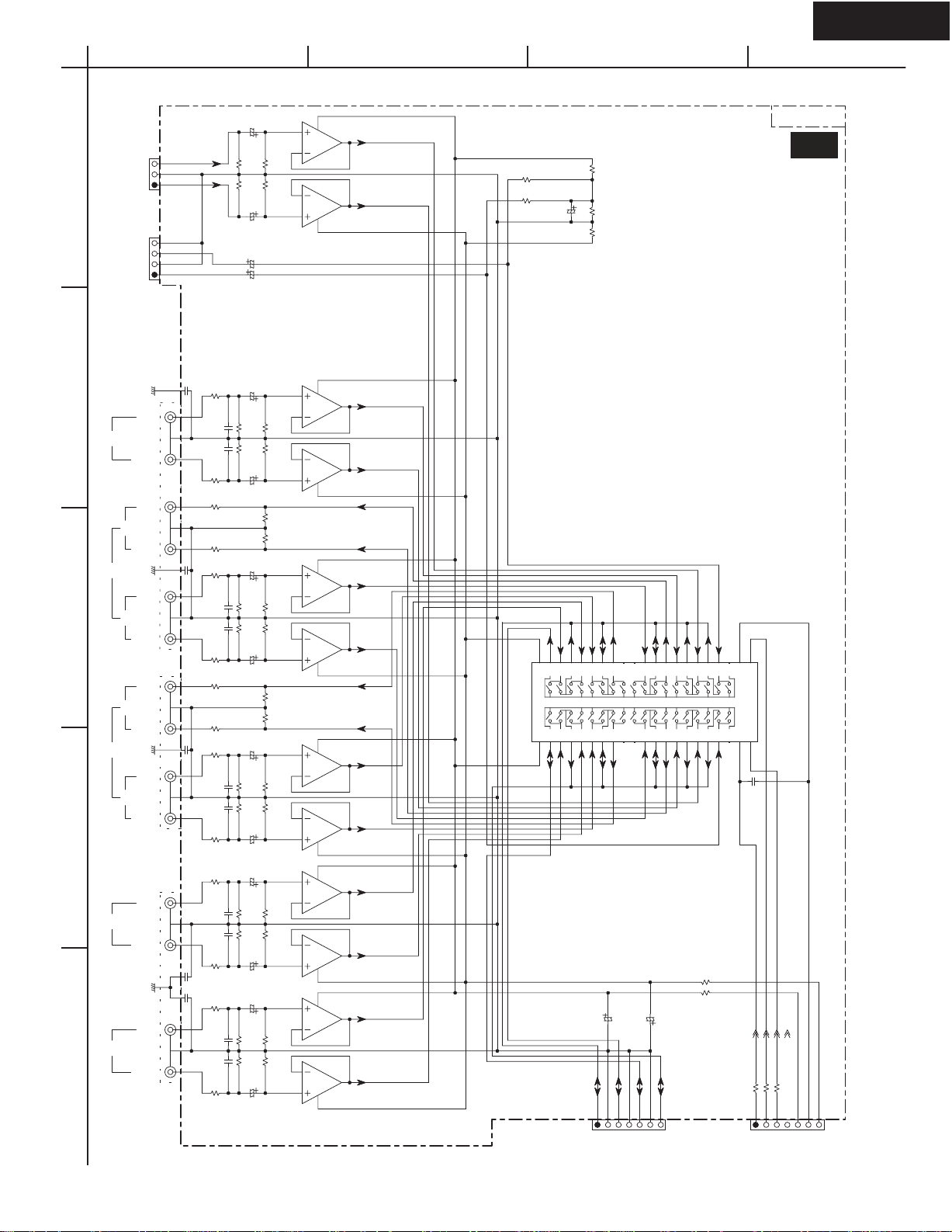
DTR-8.4
23
A
BCD
SCHEMATIC DIAGRAM 3 Audio I/O terminal section
8
3
NJM4565M-D
C3222
104Z
104Z
104Z
R3200
330
C3200
331K
C3201
331K
R3201
330
R3236
2.2K
R3237
2.2K
R3202
330
C3202
331K
C3203
331K
R3203
330
R3238
2.2K
R3239
2.2K
R3204
330
C3204
331K
C3205
331K
R3205
330
C3250
C3251
47/50
R3222
56K
R3223
56K
C3223
47/50
C3212
47/50
R3212
56K
R3213
56K
C3213
47/50
C3214
47/50
R3214
56K
R3215
56K
C3215
47/50
C3216
47/50
R3216
56K
R3217
56K
C3217
47/50
10/50
10/50
R3234
220K
R3235
220K
R3224
220K
R3225
220K
R3240
220K
R3241
220K
R3226
220K
R3227
220K
R3242
220K
R3243
220K
R3228
220K
R3229
220K
5
3
5
3
5
3
5
V5L
1
VIDEO 5
NET TUNE
2
DVD IN
REC OUT
VIDEO 1
3
PLAY IN
REC OUT
VIDEO 2
PLAY IN
(SCH. 1)
TO NAETC-7721
(SCH. 8)
TO NADG-7662
P3201
LEFT
RIGHT
LEFT
RIGHT
LEFT
RIGHT
P3202
LEFT
RIGHT
LEFT
RIGHT
P3220A
P602A
AGND
V5R
NTL
AGND
NTR
C3281
C3282
C3283
4
2
6
2
6
2
6
2
6
Q3205
Q3205
4
8
Q3200
Q3200
4
8
Q3201
Q3201
4
8
Q3202
Q3202
4
1
7
NJM4565M-D
1
7
NJM4565M-D
1
7
NJM4565M-D
1
7
R3250
100K
R3251
100K
R3252
100K
C3252
10/16
123456789
R3253
100
R3254
100K
Q3300
VDD VSS
42
10111213141516
TC9274AN-008
17
181920
2122
CL
GND
DATA
FUNC
23242526272829303132333435363738394041
C3300
101J
NAAF-7720
U13
8
3
P3203
LEFT
VIDEO 3
PLAY IN
RIGHT
LEFT
VIDEO 4
5
PLAY IN
RIGHT
C3206
C3207
C3284
104Z
C3285
104Z
C3208
C3209
R3206
330
331K
331K
R3207
330
R3208
330
331K
331K
R3209
330
C3218
47/50
R3218
56K
R3219
56K
C3219
47/50
C3220
47/50
R3220
56K
R3221
56K
C3221
47/50
R3230
220K
R3231
220K
R3232
220K
R3233
220K
2
6
5
3
2
6
5
Q3203
Q3203
4
8
Q3204
Q3204
4
NJM4565M-D
1
7
NJM4565M-D
1
7
LRZ2
AGNDLTAGNDRTAGND
TO NAAR-80
C3320
220/16
P3210B
78 (SCH. 9)
C3321
220/16
RRZ2
R3321
22
(1/2W)
R3320
22
(1/2W)
ASTB
AFCL
AFDA
+15V
MUTZ2
2.2K
2.2K
R3300
R3302
R3301 2.2K
P3211B
TO NAAR-8078 (SCH. 9)
-15V
Page 24
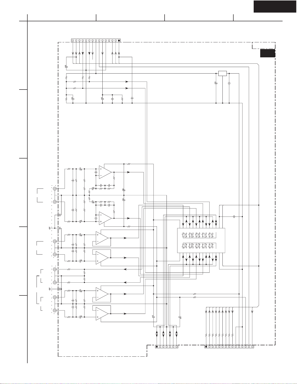
DTR-8.4
24
A
BCD
SCHEMATIC DIAGRAM 3 Audio I/O terminal section
TO TUNER P
TUL
DET
R1001
330
+5V
12VTU
ACK
FMSIG
C1003
3.3/50
VLCL
C1004
101J
VLDA
PLLCE
(CH)
R1002
100K
C1005
101J
(CH)
P1010A
SD
TUR
TMUT
STEREO
1
C1006
3.3/50
R1004
100K
R1003
100K
R1000
330
C1007
10/16
R1005
100K
R1006
100
2
C1002
10/16
Q1001
O
G
78M12
I
C1001
104Z
NAAF-7719
U12
NJM4565M-D
8
3
C3002
47/50
R3002
56K
R3014
47K
R3015
47K
R3003
56K
C3003
47/50
C3026
47/50
R3024
56K
R3025
56K
C3027
47/50
C3028
47/50
R3026
56K
R3027
56K
C3029
47/50
C3004
R3004
470K
220/6.3
220/6.3
R3005
470K
C3005
R3028
220K
R3029
220K
R3034
220K
R3035
220K
R3030
220K
R3031
220K
152J
C3006
R3006
560
R3007
560
C3007
152J
3
2
6
5
3
2
6
5
Q3000
2
C3008
123J
R3008
270K
R3009
270K
C3009
123J
6
Q3000
5
8
Q3020
Q3020
4
8
Q3021
Q3021
4
C3010
392J
R3010
22K
R3011
22K
C3011
392J
4
NJM4565M-D
1
7
NJM4565M-D
1
7
R3000
330
P3000
PHONO
CD
REC OUT
TAPE
PLAY IN
LEFT
RIGHT
C3080
104Z
LEFT
RIGHT
LEFT
RIGHT
LEFT
RIGHT
P3001
3
4
C3081
104Z
C3020
C3021
C3082
104Z
C3022
C3023
C3000
221K
C3001
221K
R3001
330
R3020
330
331K
331K
R3021
330
R3032
2.2K
R3033
2.2K
R3022
330
331K
331K
R3023
330
5
R3122
R3016
1.2K
R3017
1.2K
10
C3122
47/16
C3123
47/16
R3123
10
C3120
220/16
28
27
Q3100
VSS VDD
123456789
C3121
220/16
R3120
22
(1/2W)
R3121
22
(1/2W)
TC9273F-017
1011121314 15
ASTB
AFCL
2.2K
2.2K
2.2K
AFDA
PLLCE
2.2K
ASTB
1617181920212223242526
STB
GND
VLDA
2.2K
AFDAAFCL
VLCL
2.2K
CL DATA
TMUT
0
SD
C3100
101J
STEREO
2.2K
+15V
-15V
+5V
RDSDET
1
7
LRZ2
AGNDLTAGNDRTAGND
TO NAAR-80
P3010B
78 (SCH. 9)
RRZ2
R3102
R3100
R3101
R1012
R1011
TO NAAR-80
R1010
R1014
R1015
R1013 2.2K
P3011B
78 (SCH. 9)
Page 25
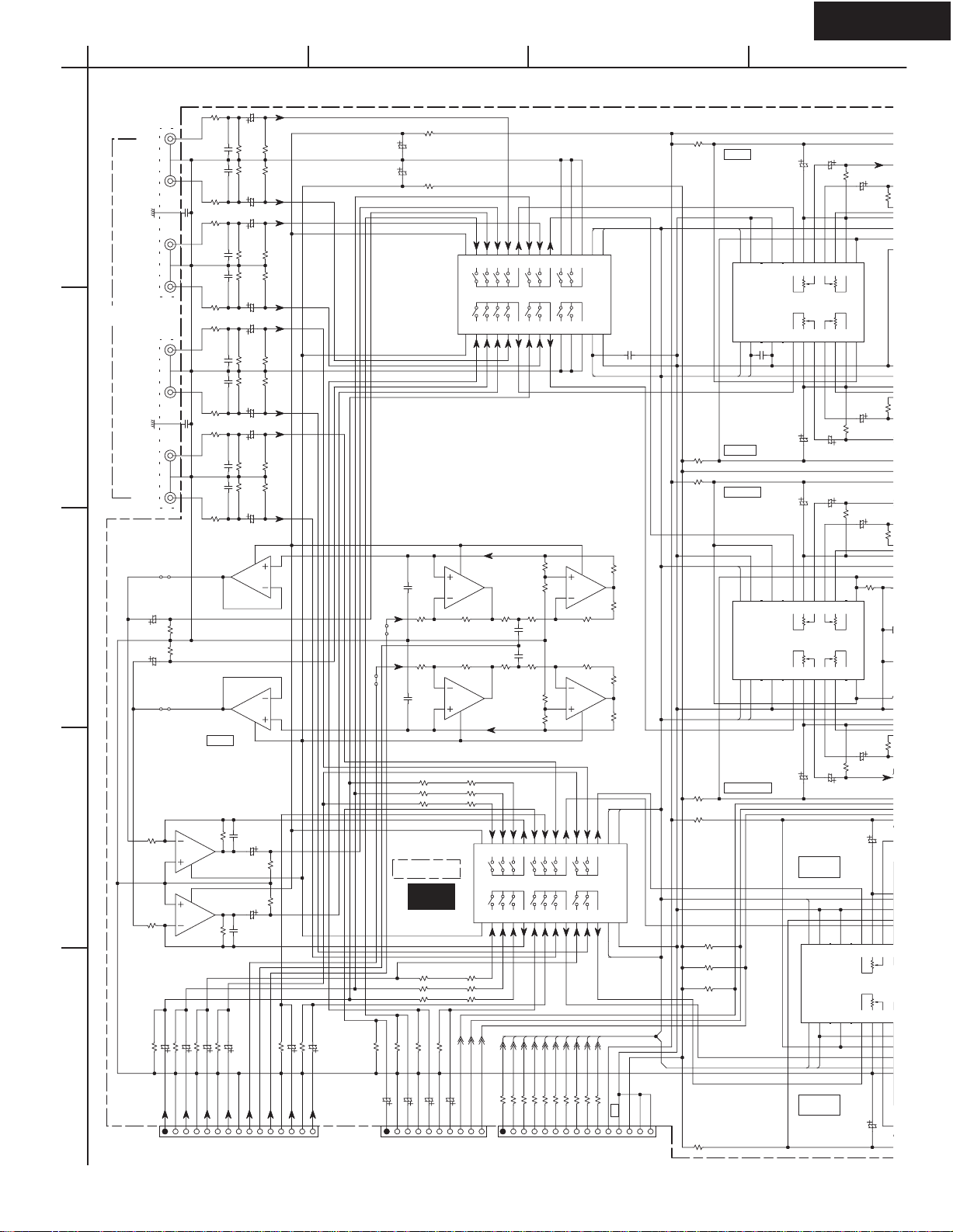
DTR-8.4
4
21
4
4
4
1
J
4
R
R
4
0
4
0
4
0
4
0
4
25
A
BCD
SCHEMATIC DIAGRAM 4 Preamplifier section
1
2
3
LEFT
FRONT
RIGHT
CENTER
SUBWOOFER
MULTICHANNEL
INPUT
LEFT
SURROUND
RIGHT
LEFT
SURROUND
BACK
RIGHT
C3800
47/50
R3800
220K
R3801
220K
C3801
47/50
P3600
P3601
J4039
J4044
C3680
104Z
C3681
104Z
R3600
C3600
331K
C3601
331K
R3601
R3602
C3602
331K
C3607
331K
R3607
R3603
C3603
331K
C3604
331K
R3604
R3605
C3605
331K
C3606
331K
R3606
330
330
330
330
330
330
330
330
VLSC
C3610
10/50
R3610
56K
R3611
56K
C3611
10/50
C3612
10/50
R3612
56K
R3617
56K
C3617
10/50
C3613
10/50
R3613
56K
R3614
56K
C3614
10/50
C3615
10/50
R3615
56K
R3616
56K
C3616
10/50
8
1
Q3862
NJM4565M-D
Q3862
7
4
R3620
220K
R3621
220K
R3622
220K
R3627
220K
R3623
220K
R3624
220K
R3625
220K
R3626
220K
3
2
6
5
C4120
220/16
C4121
220/16
J4042
J4038
R4042
R4032
R4022
C3864
R3864
R3865
C3865
R4120
22
(1/2W)
R4121
22
(1/2W)
NJM4565M-D
272J
10K
10K
272J
0
2.2K
2.2K
28
27
VDD
VSS
123456789
8
3
1
Q3860
2
R3866
10K
R3867
10K
6
Q3860
7
5
4
R4040
1.8K
12K
R4030
12K
R4020
Q4101 TC9164AF
NJM4565M-D
R3872
22K
R3874
22K
R3862
R3878
1.5K
22K
C3862
122J
C3863
122J
R3879
R3863
1.5K
22K
R3875
22K
R3873
22K
1011121314 15
R3868
8
3
Q3861
2
R3870
R3876
22K
R3877
22K
R3871
6
Q3861
5
4
R3869
AFDA
1617181920212223242526
DATA
ST
ASTB
1.5K
1.5K
1.5K
1.5K
AFCL
1
7
R4320
Left
22
(1/2W)
VLCLVLDA
10111213
NC
GNDSTB
GND CL
C4100
101J
R4321
22
(1/2W)
R4322
22
(1/2W)
R4323
22
(1/2W)
Q4200 TC94A07F
NCNCCS2 CS1
DATA CK
1415161718192021222324
VLSTB
Right
Center
VLCL
10111213
NC
GNDSTB
Q4201 TC94A07F
NCNCCS2 CS1
DATA CK
1415161718192021222324
VLDA
VLSTB
Subwoofer
C4320
220/16
C4300
C4321
220/16
C4322
220/16
C4323
220/16
C4200
10/50
C4220
R4200
100K
NC
LM
LTRT
RM
101J
R4201
100K
C4201
10/50
C4202
10/50
R4202
100K
NC
LM
LTRT
RM
R4207
100K
C4207
10/50
1/50
C4221
1/50
C4222
1/50
C4227
1/50
123456789
VSSVDD
R4541
4.7K
123456789
VSSVDD
R4210
220K
R4211
220K
R4212
220K
R4217
220K
C
1
C
1
C
1
C
1
D
5.
C
10
R
3.
C42
102
C4324
220/16
C4325
220/16
C
1
56789
NC
LMRM
C
1
AFDA
1011121314 15
TNDA
TNCL
TNCS1
2.2K
2.2K
2.2K
R4500
R4501
R4502
78 (SCH. 9)
ASTB
+15V
1617181920212223242526
DATA
ST
AFCL
GND
GND CL
-15V
R4000
C4010
4
5
R4010
10K
R4011
10K
220K
R3807
2
Q4000
3
4
NJM4565M-D
8
5
Q4000
6
R4001
220K
220K
470/6.3
R3802
R3804
C3802 47/50
C3807
DSWDCDSR
TO NAAR-8078 (SCH. 9)
10K
10K
10/50
C3804
1
7
220K
R3803
C4000
330J
C4001
330J
10/50
C3803
DSL
P4020B
10/50
R4060
R4061
C4011
10/50
DR
220K
220K
28
27
NAAF-7718
U11
2.2K
R4023
R4033 2.2K
R4043
0
220K
220K
10/50
10/50
R3806
C3806
R3805
C3805
DL
DSBL
DSBR
R3840 220K
220K
LRZ2
R3820
10/50
C3840
TO NAAR-80
LT
47/50
C3820
220K
R3821
P4010B
220K
RT
R3841
47/50
C3821
78 (SCH. 9)
VDD
VSS
123456789
12K
R4031 12K
R4041
1.8K
RRZ2
AMUT
HPMUT
Z2MUT
C3841 10/50
Q4100 TC9163AF
ASTB
AFDA
AFCL
VLCL
VLDA
VLSTB
2.2K
2.2K
2.2K
2.2K
R4103 2.2K
R4100 2.2K
R4101
R4300
R4301
R4302
TO NAAR-80
TNCS2
2.2K
R4503
P4011B
R4324
(1/2W)
R4325
(1/2W)
22
22
R4700
100K
R4701
100K
R4702
100K
Surround
Left
VLCL
10111213
NC
GNDSTB
Q4202
NCNCCS2 CS1
DATA CK
14151617181920
VLDA
VLSTB
Surround
Right
Page 26
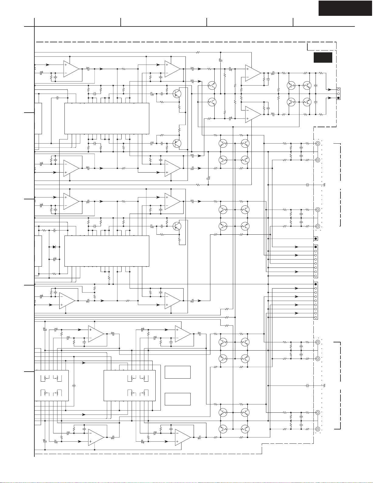
DTR-8.4
2
23
223
26
A
BCD
SCHEMATIC DIAGRAM 4 Pre amplifier section
NAAF-7718
R4920
22
(1/2W)
C4920
8
C4230
47/50
1
C4440
R4470
153J
1M
TNCS1
TNCS2
1234567
VSSVDD
24
2021
VCC ~CS
4
8
2021
VCC ~CS
1516171819
NC
VEE
fL1
fL2
fL3
TEST2
TEST1
Q4400 NJU7306G
fR3
fR2
fR1NCVSS
CLK
DI
2425262728293031323334353637383940
22
23
TNDA
TNCL
C4441
R4471
153J
1M
7
C4231
47/50
C4232
47/50
1
C4442
R4472
153J
1M
1516171819
NC
VEE
fL1
fL2
fL3
TEST2
TEST1
Q4401 NJU7306G
fR3
fR2
fR1NCVSS
CLK
DI
2425262728293031323334353637383940
22
23
TNDA
TNCL
7
C4213
100D
C4302
101J
C4237
470/6.3
3
R4237
470
Q4212
2
NJM4565M-D
R4227
8
2.2K
R4457
390
100/6.3
C4217
102J
LM
RM
C4210
100D
C4211
100D
C4212
100D
C4501
101J
D4540
5.1B
C4540
R4540
3.3K
C4203
10/50
R4203
C4500
101J
100K
6
5
LTRT
3
Q4210
2
NJM4565M-D
6
Q4210
5
3
Q4211
2
NJM4565M-D
Q4211
4
C4223
1/50
R4213
220K
C4220
1/50
1
R4210
220K
1
VSSVDD
7F
24
2
R4211
220K
C4221
1/50
C4222
1/50
R4212
220K
R4541
4.7K
1
3
VSSVDD
7F
24
R4217
220K
C4227
1/50
C4324
4
20/16
8
NCNC
2 TC94A07F
17181920212223
R4410
4.7K
R4430
R4480
R4481
R4482
220K
390
1011121314
fL4
fL5
fL6
fL7
fL8
fL9
fL10
fR10
fR9
fR8
fR7
fR6
fR5
fR4
390
R4431
220K
R4411
4.7K
R4412
4.7K
R4432
220K
390
1011121314
fL4
fL5
fL6
fL7
fL8
fL9
fL10
fR10
fR9
fR8
fR7
fR6
fR5
fR4
R4417
4.7K
1
C4233
47/50
VLCL
10111213
NC
NC
GNDSTB
Q4203 TC94A07F
NCNCCS2 CS1
DATA CK
1415161718192021222324
VLDA
VLSTB
fL11
fR11
fL11
fR11
R4420
4.7K
C4410
101K
C4420
47/50
123456789
NC
VDD
IN1L
IN2L
NC
IN1R
IN2R
NC
C4421
47/50
C4411
101K
R4421
4.7K
R4422
4.7K
C4412
101K
C4422
47/50
123456789
NC
VDD
IN1L
IN2L
NC
IN1R
IN2R
NC
C4417
102J
R4427
4.7K
C4205
10/50
C4225
R4205
1/50
100K
R4215
220K
LM
LTRT
RM
123456789
VSSVDD
R4440
47K
C4430
104J
R4450
390
R4451
390
C4431
104J
R4441
47K
R4442
47K
C4432
104J
R4452
390
3
Q4410
2
NJM2082M-D
Q4420
R4460
2SA1163-BL
2SA1163-BL
R4461
Q4421
6
Q4410
5
3
Q4411
2
NJM2082M-D
Q4422
R4462
2SA1163-BL
6
Q4411
5
C4215
100D
Surround B ack
/ Zone2
Surround B ack
/ Zone2
8
4.7K
4.7K
4
8
4.7K
4
3
2
Left
Right
1
7
1
7
8
Q4213
NJM4565M-D
C4800
10/16
C4600
47/50
C4801
10/16
C4601
47/50
C4602
47/50
C4607
47/50
1
R4921
C4235
47/50
R4800
22K
RN1441
Q4810
Q4811
RN1441
R4801
22K
22
(1/2W)
5
C4325
20/16
R4204
100K
C4204
10/50
R4214
220K
C4224
1/50
C4214
100D
C4234
6
Q4212
5
47/50
7
4
R4206
100K
C4206
10/50
R4216
220K
C4226
1/50
C4216
100D
6
Q4213
7
5
C4236
47/50
4
220/16
R4600
R4601
C4921
220/16
R4602
R4607
R4603
R4604
R4605
R4606
C4802
2.2/50
R4802
22K
R4804
220K
R4805
220K
22K
C4803
2.2/50
270
RN1441
Q4600
Q4601
RN1441
270
270
RN1441
Q4602
Q4607
RN1441
270
R4712
1K
R4710
1.5K
R4711
3.9K
270
RN1441
Q4603
Q4604
RN1441
270
270
RN1441
Q4605
Q4606
RN1441
270
R4610
100
Q4610
RN1441
RN1441
Q4611
R4611
100
R4612
100
Q4612
RN1441
RN1441
Q4617
R4617
100
R4613
100
Q4613
RN1441
RN1441
Q4614
R4614
100
R4615
100
Q4615
RN1441
RN1441
Q4616
R4616
100
3
2
R4808
2.2K
R4809
2.2K
6
5
8
Q4800
Q4800
4
NJM4565M-D
1
R4806
10K
R4807
10K
7
C4806
100/6.3
C4804
101K
R4812
10K
R4813
C4805
101K
C4807
100/6.3
R4810
33
Q4812
RN1441
RN1441
10K
Q4813
R4811
33
C4610
R4640
R4620
47
22K
R4621
R4641
47
22K
C4611
C4612
R4622
R4642
47
22K
R4647
R4627
47
22K
C4617
C4613
R4623
R4643
47
22K
R4644
R4624
47
22K
C4614
C4615
R4645
R4625
47
22K
R4646
R4626
47
22K
C4616
R4814
Q4814
RN1441
RN1441
Q4815
R4815
102J
102J
102J
102J
SBRAI
SBLAI
102J
102J
102J
102J
33
33
R4630
R4631
C4680
104Z
R4632
R4637
AGND
RAI
LAI
CAI
SRAI
SLAI
R4633
R4634
C4681
104Z
R4635
R4636
47
47
47
47
47
47
47
47
U11
R4816
33
C4808
222J
C4809
222J
R4817
33
P4600
LEFT
RIGHT
CENTER
SUBWOOFER
P6101A
P5003E
TO NAAF-7706 (SCH. 6)
06 (SCH. 6)
P5004E
TO NAAF-77
P4601
LEFT
RIGHT
LEFT
RIGHT
HPL
HPR
PREOUT
SURROUND
PREOUT
SURROUND
BACK
/ZONE2
P4012A
TO NAAR-8078 (SCH. 9)
Page 27
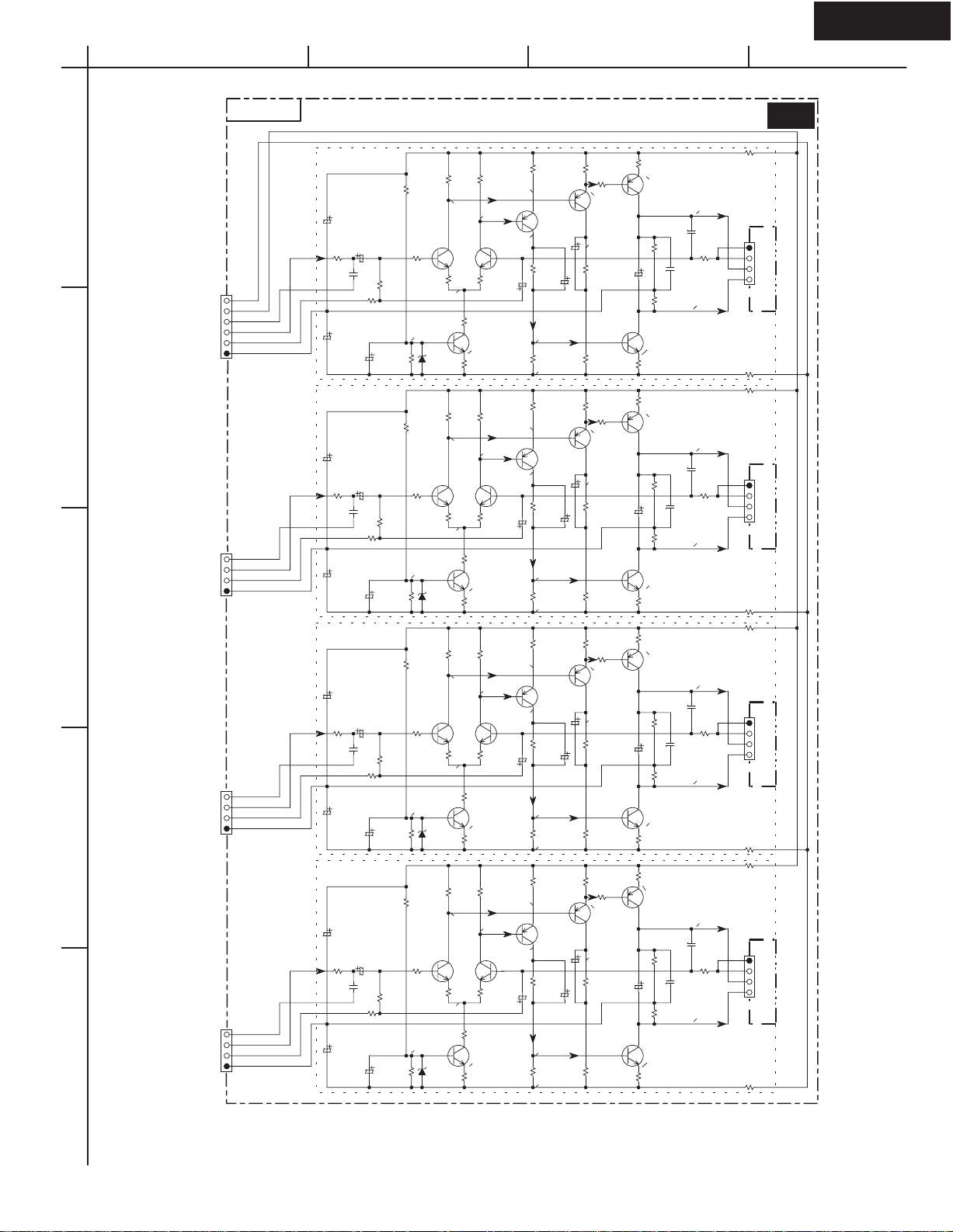
DTR-8.4
27
A
SCHEMATIC DIAGRAM 5 Driver section
NAAF-7707
SL
1
C5123
47/100
C5003
R5003
10/50
1K
C5013
-B1
+B1
(SCH. 6)
TO NAAF-7706
2
3
4
5
P6013A
(SCH. 6)
TO NAAF-7706
P6014AP6015A
(SCH. 6)
TO NAAF-7706
(SCH. 6)
TO NAAF-7706
P6016A
221K
C5133
47/100
SR
C5124
47/100
R5004
C5014
221K
C5134
47/100
SBL
C5125
47/100
R5005
C5015
221K
C5135
47/100
SBR
C5126
47/100
R5006
C5016
221K
C5136
47/100
C5053
10/50
1K
C5054
10/50
1K
C5055
10/50
1K
C5056
10/50
C5004
10/50
C5005
10/50
C5006
10/50
BCD
U22
R5013
56K
R5093
1.8K
R5293
100K
R5014
56K
R5094
1.8K
R5294
100K
R5015
56K
R5095
1.8K
R5295
100K
R5016
56K
R5096
1.8K
R5296
100K
R5073
100K
R5023
330
-52.6V
R5074
100K
R5024
330
-52.6V
R5075
100K
R5025
330
-52.6V
R5076
100K
R5026
330
-52.6V
R5033
120
-0.9V
D5003
MTZJ5.6B
R5034
120
-0.9V
D5004
MTZJ5.6B
Q5005
R5035
120
-0.9V
D5005
MTZJ5.6B
R5036
120
-0.9V
D5006
MTZJ5.6B
R5113
2.2K
56.1V
R5043
R5114
2.2K
56.1V
R5044
R5115
2.2K
56.1V
C5035
R5045
R5116
2.2K
56.1V
R5046
120
R5053
120
R5054
120
R5055
120
R5056
5.6K
-53.3V
R5063
2.7K
5.6K
-53.3V
R5064
2.7K
5.6K
-53.3V
R5065
2.7K
5.6K
-53.3V
R5066
2.7K
R5123
2.2K
56.0V
Q5013Q5003
100/16
Q5023
R5124
2.2K
56.0V
Q5014Q5004
100/16
Q5024
R5125
2.2K
56.0V
100/16
Q5025
R5126
2.2K
56.0V
Q5016Q5006
100/16
Q5026
C5043
C5044
Q5015
C5045
C5046
R5143
820
(1/4W)
56.6V
Q5043
-39.3V
R5173
820
(1/4W)
R5144
820
(1/4W)
56.6V
Q5044
-39.3V
R5174
820
(1/4W)
R5145
820
(1/4W)
56.6V
Q5045
-39.3V
R5175
820
(1/4W)
R5146
820
(1/4W)
56.6V
Q5046
-39.3V
R5176
820
(1/4W)
R5283
10K
(1/2W)
-55.9V
-57.5V
R5284
10K
(1/2W)
-55.9V
-57.5V
R5285
10K
(1/2W)
-55.9V
-57.5V
R5286
10K
(1/2W)
-55.9V
-57.5V
(1/4W)
10/100
C5083
22/63
(1/4W)
10/100
C5084
22/63
(1/4W)
10/100
C5085
22/63
(1/4W)
10/100
C5086
22/63
R5133
820
C5073
R5134
820
C5074
R5135
820
C5075
R5136
820
C5076
R5183
33
(1/4W)
55.9V
Q5033
-39.2V
R5153
10K
(1/2W)
R5163
1K
(1/4W)
R5184
33
(1/4W)
55.9V
Q5034
-39.2V
R5154
10K
(1/2W)
R5164
1K
(1/4W)
R5185
33
(1/4W)
55.9V
Q5035
-39.2V
R5155
10K
(1/2W)
R5165
1K
(1/4W)
R5186
33
(1/4W)
55.9V
Q5036
-39.2V
R5156
10K
(1/2W)
R5166
1K
(1/4W)
C5093
47/50
Q5083
C5094
47/50
Q5084
C5095
47/50
Q5085
C5096
47/50
Q5086
R5303
100
(1/4W)
56.5V
Q5053
R5213
18K
R5223
18K
-56.5V
R5333
100(1/4W)
R5304
(1/4W)
100
56.5V
Q5054
R5214
18K
R5224
18K
-56.5V
R5334
100(1/4W)
R5305
(1/4W)
100
56.5V
Q5055
R5215
18K
R5225
18K
-56.5V
R5335
100(1/4W)
R5306
(1/4W)
100
56.5V
Q5056
R5216
18K
R5226
18K
-56.5V
R5336
100(1/4W)
C5113
050D
C5114
050D
C5115
050D
C5116
050D
C5103
101K
C5104
101K
C5105
101K
C5106
101K
1.2V
R5253
56K
-1.2V
1.2V
R5254
56K
-1.2V
1.2V
R5255
56K
-1.2V
1.2V
R5256
56K
-1.2V
NF
NF
B+
B-
NF
NF
B+
B-
NF
NF
B+
B-
NF
NF
B+
B-
R5233
(1/4W)
P6003A
R5243
(1/4W)
R5234
(1/4W)
P6004A
R5244
(1/4W)
R5235
(1/4W)
P6005A
R5245
(1/4W)
R5236
(1/4W)
P6006A
R5246
(1/4W)
15
(SCH. 6)
TO NAAF-7706
15
15
(SCH. 6)
TO NAAF-7706
15
15
(SCH. 6)
TO NAAF-7706
15
15
(SCH. 6)
TO NAAF-7706
15
.
.
.
.
.
.
.
Page 28
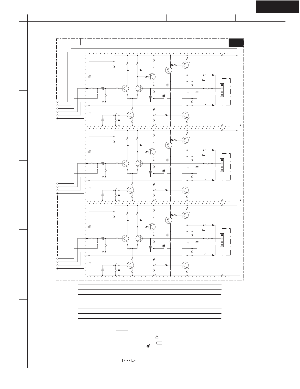
DTR-8.4
28
A
SCHEMATIC DIAGRAM 5 Driver section
NAAF-7690
C5120
100/100
R5000
C5010
101K
C5130
100/100
L
1K
C5050
10/50
C5000
22/35
R5010
R5090
1.8K
56K
R5290
100K
R5070
100K
R5020
330
-52.1V
1
P6010A
-B1
+B1
(SCH. 6)
TO NAAF-7706
2
R
R5071
100K
C5121
100/100
C5001
R5001
22/35
1K
R5021
C5061
C5051
10/50
C
1K
C5052
10/50
R5011
R5091
1.8K
C5002
22/35
R5012
R5092
1.8K
56K
R5291
100K
56K
R5292
100K
330
-52.1V
R5072
100K
R5022
330
-52.1V
C5011
101K
C5131
3
4
(SCH. 6)
TO NAAF-7706
P6011A
(SCH. 6)
TO NAAF-7706
P6012A
100/100
C5122
100/100
R5002
C5012
221K
C5132
100/100
BCD
U26
R5300
68
C5090
47/50
Q5080
C5091
47/50
Q5081
C5092
47/50
Q5082
(1/4W)
56.6V
Q5050
R5210
18K
-56.6V
R5330
68 (1/4W)
R5301
(1/4W)
68
56.6V
Q5051
R5211
18K
-56.6V
R5331
68 (1/4W)
R5302
68 (1/4W)
56.6V
Q5052
R5212
18K
-56.6V
R5332
68 (1/4W)
C5110
050D
R5220
18K
C5111
050D
R5221
18K
C5112
050D
R5222
18K
C5100
101K
C5101
101K
C5102
101K
33
33
33
1.2V
R5250
56K
-1.2V
1.2V
R5251
56K
-1.2V
1.2V
R5252
56K
-1.2V
NF
NF
B+
NF
NF
B+
B-
NF
NF
B+
B-
R5230
(1/4W)
B-
(1/4W)
R5231
(1/4W)
(1/4W)
R5232
(1/4W)
(1/4W)
15
P6000A
R5240
15
15
P6001A
R5241
15
15
P6002A
R5242
15
(SCH. 6)
TO NAAF-7706
(SCH. 6)
TO NAAF-7706
(SCH. 6)
TO NAAF-7706
Q5000
R5030
330
-0.9V
Q5020
D5000
MTZJ5.6B
R5031
330
-0.9V
Q5021
D5001
MTZJ5.6B
R5032
330
-0.9V
Q5022
D5002
MTZJ5.6B
R5110
2.2K
55.8V
R5040
330
R5111
2.2K
55.8V
R5041
330
R5112
2.2K
55.8V
C5032
R5042
330
R5050
5.6K
-52.6V
R5060
2.7K
R5051
5.6K
-52.6V
R5061
2.7K
R5052
5.6K
-52.6V
R5062
2.7K
R5120
2.2K
55.7V
Q5010
C5040
220/16
R5121
2.2K
55.7V
Q5011Q5001
C5041
220/16
R5122
2.2K
55.7V
Q5012Q5002
C5042
220/16
R5140
820
(1/4W)
51.5V
Q5040
-39.0V
R5170
820
(1/4W)
R5141
820
(1/4W)
51.5V
Q5041
-39.0V
R5171
820
(1/4W)
R5142
820
(1/4W)
51.5V
Q5042
-39.0V
R5172
820
(1/4W)
57.5V
R5280
10K
(1/2W)
-55.9V
-57.5V
57.5V
R5281
10K
(1/2W)
-55.9V
-57.5V
57.5V
R5282
10K
(1/2W)
-55.9V
-57.5V
(1/4W)
10/100
C5080
22/63
(1/4W)
10/100
C5081
22/63
(1/4W)
10/100
C5082
22/63
R5130
820
C5070
R5131
820
C5071
R5132
820
C5072
R5180
(1/4W)
56.3V
Q5030
-38.9V
R5150
10K
(1/2W)
R5160
1K
(1/4W)
R5181
(1/4W)
56.3V
Q5031
-38.9V
R5151
10K
(1/2W)
R5161
1K
(1/4W)
R5182
(1/4W)
56.3V
Q5032
-38.9V
R5152
10K
(1/2W)
R5162
1K
(1/4W)
CIRCUIT NO. DESCRIPTION
Q5000~Q5006,Q5010~Q5016 KTC3200-BL OR 2SC1775A-E OR 2SC1775A-F OR 2SC1845-E
Q5020~Q5026 KTC3200-BL OR 2SC1775A-E OR 2SC1775A-F OR 2SC1845-E
Q5030~Q5036,Q5040~Q5046 KTA1024-Y OR KTA1024-O OR 2SA949-Y OR 2SA949-O
Q5050~Q5052 2SA1360-Y OR 2SA1360-O
Q5053~Q5056 KTA1024-Y OR KTA1024-O OR 2SA949-Y OR 2SA949-O
Q5080~Q5082 2SC3423-Y OR 2SC3423-O
Q5083~Q5086 KTC3206-Y OR KTC3206-O OR 2SC2229-Y OR 2SC2229-O
.
NOTE
5
.
.
THE COMPONENTS IDENTIFIED BY MARK ! ARE CRITICAL FOR SAFETY.
REPLACE ON LY WITH PART NUMBER SPECIFIED.
.
VOLTAGE (MEASURED WITH VOLTMETER) IS DC VOLTAGE (NO INPUT SIGNAL)
ELECTROLYTIC CAPACITORS ( ) ARE IN uF/WV.
.
ALL CAPACITORS ARE IN pF/50WV UNLESS OTHERWISE NOTED.
.
EX) 030-3pF 330-33pF 331-330pF 333pF-0.033uF
ALL RESISTORS ARE IN OHMS 1/4WATTS UNLESS OTHERWISE NOTED.
.
THE THICK LINE ON PC BOARD ARE THE PRINTING SIDE OF THE PARTS.
EX) PRINTING SIDE
CIRCUIT IS SUBJECT TO CHANGE FOR IMPROVEMENT.
Page 29
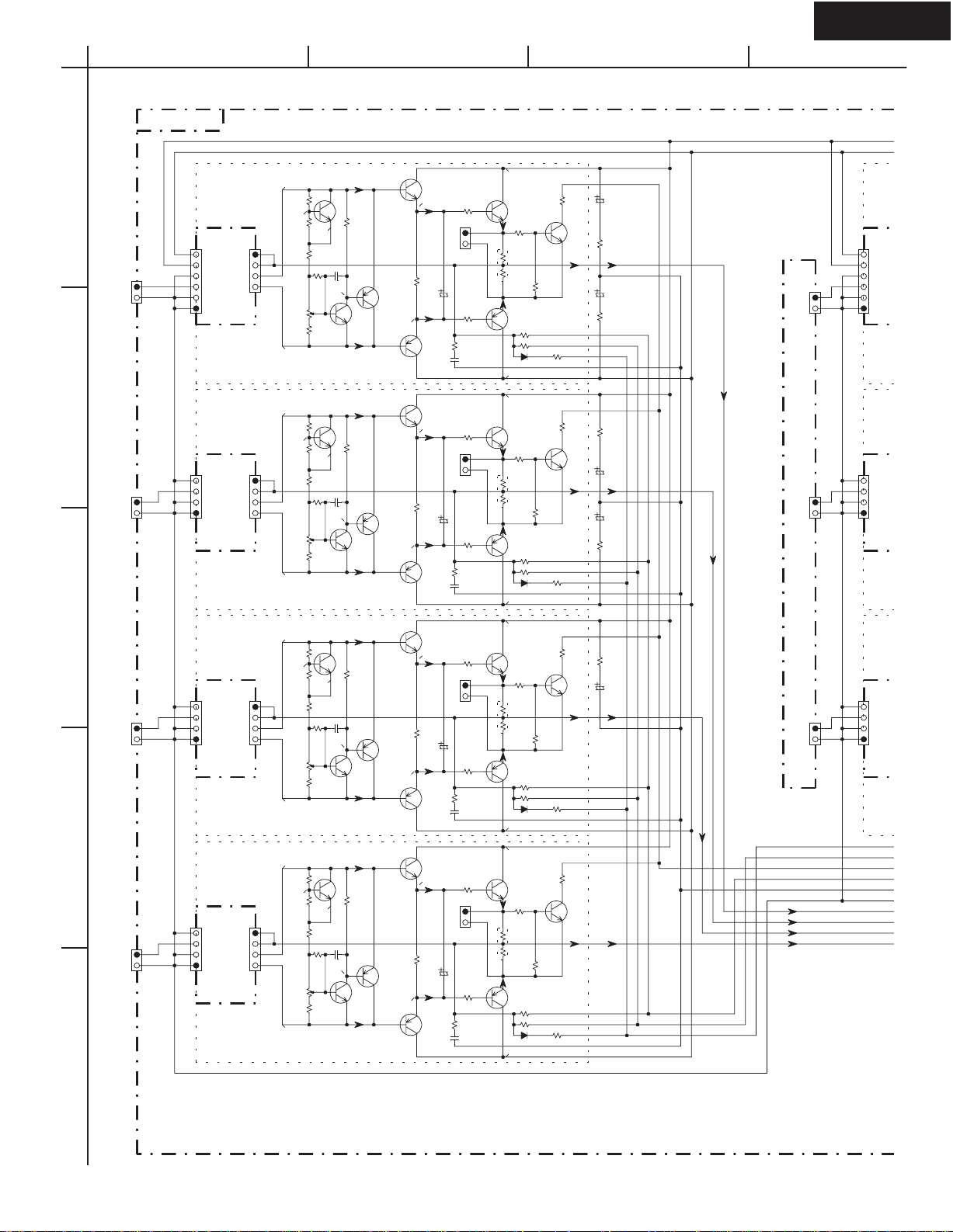
DTR-8.4
29
A
BCD
SCHEMATIC DIAGRAM 6 Power amplifier section
NAAF-7706
1
P5004A
(SCH. 3)
TO NAAF-7718
2
(SCH. 3)
TO NAAF-7718
3
P5004CP5004D P5004B
(SCH. 3)
TO NAAF-7718
4
(SCH. 3)
TO NAAF-7718
5
SL
P6003
-B1 -B1
+B1 +B1
E E
E E
TO NAAF-7707
E E
P6013
SR
E E
E E
E E
TO NAAF-7707
P6014
SBL
E E
E E
E E
TO NAAF-7707
P6015
SBR
E
E
E
TO NAAF-7707
P6016
(SCH. 5)
(SCH. 5)
(SCH. 5)
(SCH. 5)
NF
NF
B+
(SCH. 5)
B-
TO NAAF-7707
P6004
NF
NF
B+
(SCH. 5)
B-
TO NAAF-7707
P6005
NF
NF
B+
(SCH. 5)
B-
TO NAAF-7707
P6006
NF
NF
B+
(SCH. 5)
B-
TO NAAF-7707
1.2V
R6013
5.6K
0.5V
R6023
3.9K
R6033
1K
R6113
R6043
1K
R6053
2.7K
-1.2V
1.2V
R6014
5.6K
0.5V
R6024
3.9K
R6034
1K
R6114
R6044
1K
R6054
2.7K
-1.2V
1.2V
R6015
5.6K
0.5V
R6025
3.9K
R6035
1K
R6115
R6045
1K
R6055
2.7K
-1.2V
1.2V
R6016
5.6K
0.5V
R6026
3.9K
R6036
1K
R6116
R6046
1K
R6056
2.7K
-1.2V
10K
10K
10K
10K
0.1V
0.1V
0.1V
0.1V
Q6003
C6003
Q6013
Q6004
C6004
Q6014
Q6005
C6005
Q6015
Q6006
C6006
Q6016
102J
0.6V
102J
0.6V
102J
0.6V
102J
0.6V
R6063
3.3K
Q6023
R6064
3.3K
Q6024
R6065
3.3K
Q6025
R6066
3.3K
Q6026
R6073
(1/4W)
0.6V
Q6043
R6074
(1/4W)
0.6V
Q6044
R6075
(1/4W)
0.6V
Q6045
R6076
(1/4W)
0.6V
Q6046
180
180
180
180
Q6033
0.6V
C6023
47/50
R6133
(1W)
C6033
473J/100
Q6034
0.6V
C6024
47/50
R6134
(1W)
C6034
473J/100
Q6035
0.6V
C6025
47/50
R6135
(1W)
C6035
473J/100
Q6036
0.6V
C6026
47/50
R6136
(1W)
C6036
473J/100
R6083
(1/4W)
P6083
ID+
ID-
R6093
(1/4W)
8.2
R6084
(1/4W)
P6084
ID+
ID-
R6094
(1/4W)
8.2
R6085
(1/4W)
P6085
ID+
ID-
R6095
(1/4W)
8.2
R6086
(1/4W)
P6086
ID+
ID-
R6096
(1/4W)
8.2
58.3V
R6163
Q6053
2.2
2.2
Q6063
2.2
2.2
Q6064
2.2
2.2
Q6065
2.2
2.2
Q6066
R6143
22K
R6103
0.22
X2
R6153
4.7K
R6193
-58.3V
58.3V
Q6054
R6144
22K
R6104
0.22
X2
R6154
4.7K
R6194
-58.3V
58.3V
Q6055
R6145
22K
R6105
0.22
X2
R6155
4.7K
R6195
-58.3V
58.3V
Q6056
R6146
22K
R6106
0.22
X2
R6156
4.7K
R6196
-58.3V
(5W)
47K
(5W)
47K
(5W)
47K
(5W)
47K
33K
Q6073
R6203
D6003
R6164
33K
Q6074
R6204
D6004
R6165
33K
Q6075
R6205
D6005
R6166
33K
Q6076
R6206
D6006
47K
R6213
47K
47K
R6214
47K
47K
R6215
47K
47K
R6216
47K
C6512
4.7/100
R6512
0.22
(1/2W)
C6522
4.7/100
R6522
0.22
(1/2W)
R6513
0.22
(1/2W)
R6523
0.22
(1/2W)
R6514
0.22
(1/2W)
C6513
4.7/100
C6523
4.7/100
C6514
4.7/100
(SCH. 3)
TO NAAF-7718
P5003BP5003C P5003A
(SCH. 3)
TO NAAF-7718
(SCH. 3)
TO NAAF-7718
TO NAAF-7690
P6010
TO NAAF-7690
P6011
TO NAAF-7690
P6012
(SCH. 5)
(SCH. 5)
(SCH. 5)
Page 30
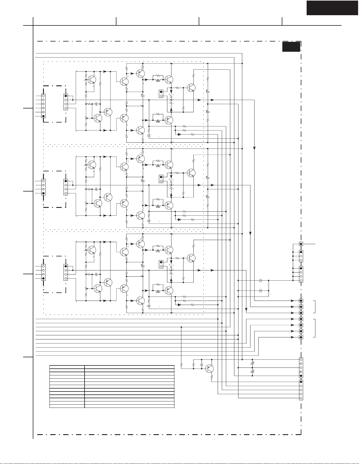
DTR-8.4
30
A
BCD
SCHEMATIC DIAGRAM 6 Power amplifier section
R6060
120
Q6020
R6061
120
Q6021
R6062
120
Q6022
R6230
120
(1/4W)
Q6030
R6070
68
(1/4W)
R6240
120
(1/4W)
R6231
120
(1/4W)
Q6031
R6071
68
(1/4W)
R6241
120
(1/4W)
R6232
120
(1/4W)
Q6032
R6072
68
(1/4W)
R6242
120
(1/4W)
58.2V
57.7V
R6250
18
(1/4W)
C6020
4.7/160
R6260
18
(1/4W)
-57.7V
Q6100
R6280
2.2
(1/4W)
58.2V
57.7V
R6251
18
(1/4W)
C6021
4.7/160
R6261
18
(1/4W)
-57.7V
Q6101
R6281
2.2
(1/4W)
58.2V
57.7V
R6252
18
(1/4W)
C6022
4.7/160
R6262
18
(1/4W)
-57.7V
Q6102
R6282
2.2
(1/4W)
-0.6V
-0.6V
-0.6V
R6270
2.2
(1/4W)
Q6090
0.6V
R6271
2.2
(1/4W)
Q6091
0.6V
R6272
2.2
(1/4W)
Q6092
0.6V
R6080
10
(1/2W)
L6000
ID+
ID-
R6090
10
(1/2W)
L6010
R6130
8.2
C6030
473J/100
R6081
10
(1/2W)
L6001
ID+
ID-
R6091
10
(1/2W)
L6011
R6131
8.2
C6031
473J/100
R6082
10
(1/2W)
L6002
ID+
ID-
R6092
10
(1/2W)
L6012
R6132
8.2
C6032
473J/100
P6080
(1W)
P6081
(1W)
P6082
(1W)
Q6050
R6140
R6100
Q6060Q6040
-58.3V
Q6051
R6141
R6101
Q6061Q6041
-58.3V
Q6052
R6142
R6102
Q6062Q6042
-58.3V
E
E
E
P6010
E
E
E
P6011
E
E
E
P6012
L
(SCH. 5)
(SCH. 5)
TO NAAF-7690
TO NAAF-7690
R
(SCH. 5)
(SCH. 5)
TO NAAF-7690
TO NAAF-7690
C
(SCH. 5)
(SCH. 5)
TO NAAF-7690
TO NAAF-7690
P6000
NF
NF
B+
B-
P6001
NF
NF
B+
B-
P6002
NF
NF
B+
B-
1.2V
R6010
4.7K
0.5V
R6020
3.3K
R6030
1.8K
R6110
10K
R6040
1K
R6050
2.7K
-1.2V
1.2V
R6011
4.7K
0.5V
R6021
3.3K
R6031
1.8K
R6111
10K
R6041
1K
R6051
2.7K
-1.2V
1.2V
R6012
4.7K
0.5V
R6022
3.3K
R6032
1.8K
R6112
10K
R6042
1K
R6052
2.7K
-1.2V
Q6000
0.1V
Q6001
0.1V
Q6002
0.1V
C6000
102J
0.6V
Q6010
C6001
102J
0.6V
Q6011
C6002
102J
0.6V
Q6012
1
-B1
+B1
2
3
4
58.3V
22K
0.22
X2
(5W)
R6150
4.7K
58.3V
22K
0.22
X2
(5W)
R6151
4.7K
58.3V
22K
0.22
(5W)
X2
R6152
4.7K
R6160
Q6070
R6190
47K
D6000
R6161
Q6071
R6191
47K
D6001
R6162
Q6072
R6192
47K
D6002
33K
C6040
R6200
33K
C6041
R6201
33K
R6202
47K
R6210
47K
47K
R6211
47K
47K
R6212
47K
R6510
0.22
(1/2W)
R6520
0.22
(1/2W)
R6511
0.22
(1/2W)
R6521
0.22
(1/2W)
C6510
4.7/100
C6520
4.7/100
C6511
4.7/100
C6521
4.7/100
C6531
103J
C6532
103J
U21
P6101
P6007
TO NAETC-7694
(SCH. 7)
P6008
TO NAETC-7695
(SCH. 7)
P6810A
P6810B
P6810C
P6812A
P6812B
P6812C
P6812D
TO NAAF-7718
(SCH. 3)
TO NAETC-7694
(SCH. 7)
TO NAETC-7695
(SCH. 7)
+B1 +B1
10K
R6702
C6703
223Z
Q6703
47K
R6704
CIRCUIT NO. DESCRIPTION
Q6000~Q6006,Q6010~Q6016 2SC1740S-R OR 2SC1740-S
Q6020~Q6022 KTA1267-GR OR 2SA933S-R OR 2SA933S-S OR 2SA1048-GR
Q6023~Q6026 2SA1015-GR OR 2SA1015-Y
Q6030~Q6032 2SC2229-Y OR 2SC2229-O
Q6033~Q6036,Q6100~Q6102 KTD2061-Y OR 2SC5171
Q6040~Q6042 2SA949-Y OR 2SA949-O
Q6043~Q6046 KTB1369-Y OR 2SA1930
Q6050~Q6056 2SC5359-O OR 2SC5359-R
5
Q6060~Q6066 2SA1987-O OR 2SA1987-Y
Q6070~Q6076 2SC2631-R OR 2SC2631-S
Q6090~Q6092 KTB1369-Y OR 2SA1930
Q6703 KTA1268-GR OR KTA1268-BL OR 2SA992-E OR 2SA992-F
22K
R6701
C6901
15000/71
C6902
15000/71
E
-B1
PRO
DCDET
FANDET
VOLH
E
P6952
TO NAPS-7692
(SCH. 7)
P6931
TO NAETC-7696
(SCH. 7)
Page 31

DTR-8.4
P9501
S
C
C
C
8
8
8
8
U
U
N
N
K
Y
Y
31
A
BCD
SCHEMATIC DIAGRAM 7 Power supply and speaker terminal sections
D6904
RBV-1506
D15XB60
D6901,2:
GP1004003E
RL1N4003
1SR139-100
Q5602:
Q5601
D5602
R6710
18K
P TYPE
L6800 S1.3C
R6800
R6810
D TYPE
P TYPE
L6801
R6801
R6811
D TYPE
P TYPE
L6802
R6802
R6812
D TYPE
D6903
RBV-1506
D15XB60
2SC1740S
OR 2SC2458
OR KTC3199
Q5602
2SK365-GR
Q5608,9:
DTC144ES
OR RN1204
OR KRC104M
C6705
223Z
10K
R6707
R6708
33K
5.6K
R6709
D6704
MTZJ5.1B
J
J
J
F6902
C6911
C6910
R5604
10K
C6706
100/6.3
22
22
S1.3C
22
22
S1.3C
22
22
C5602
100/35
Q5609
334J
334J
F6901
*
R5605
100
COM
TH2
TH1
22K
MTZJ5.1B
*
U30
(1W)
8.2
R6831
8.2
R6832
(1W)
C6831
103J
C6832
RL6902
C6909
C6908
RL6901
Q5603,7: 2SC1740S
R5615
R5614
10K
2.7K
Q5608
Q5607
P6401
Q6704
2SA933S 2SA1048
R6705
18K
Q6702
C6704
1/50
R6706
D6702
D6703
Q6701,6702
P6800
SPEAKERS
L
R
C
C6842 102J *
C6840 102J
C6841 102J
C6852 102K
8.2
(1W)
R6830
C6851 102K
C6850 102K *
C6830
103J
103J
* P TYPE
S1H1
RED
R5606
10K
KTA1267
:
D6906
103Z
C6912
GND
S1H2
BLK
RED
FAN CONTROL
R5608
R5609
10K
D5604
D5609
R5607
2.7K
Q5603
PRO FAN
VOLH
Q6701
D6701
C6701
100/6.3
334J/100
334J/100
P6951
OR 2SC2458
OR KTC3199
D5605
D5606
D5607
2SC1740S 2SC2458 KTC3199
*
*
*
*
U28
S1L1
S1L2
ORG
ORG
10K
D5610
Q5604
DTC144ES
OR RN1204
OR KRC104M
R5616
1.2K
(2W)
NAETC-7694
C6600
1
P6810D
LSP
RSP
CSP
(SCH. 6)
TO NAAF-7706
P6007A
LSPE
RSPE
CSPE
(SCH. 6)
TO NAAF-7706
2
P6830
103Z
D6600
RL6600
RL6602
TO NAETC-8083
(SCH. 9)
NAPS-7692
C6915
334J
/100
+B1
GND
C6916
(SCH. 6)
TO NAAF-7706
3
334J
-B1
/100
P6952A
D6901
C6903
223J
D6902
P6906
FAN CONTROL
SIGNAL TEMP Q5601 Q5602 Q5603 Q5604 Q5605 Q5607 Q5608 Q5609 Q5606 FAN
NO LOW ON OFF OFF ON ON OFF ON OFF 0V OFF
YES LOW OFF ON OFF OFF ON OFF ON OFF 12V LOW
NO MID ON OFF ON OFF ON OFF ON OFF 12V LOW
YES MID OFF ON ON OFF OFF OFF ON OFF 22V HI
NO HIGH ON OFF ON OFF OFF ON OFF ON 22V HI
YES HIGH OFF ON ON OFF OFF ON OFF ON 22V HI
NAETC-7696
R5603
R5602
1M
33K
R5601
D5603
GP1004003E
RL1N4003
1SR139-100
100K
D5601
:
4
C5601
D5602-5603
5
P6931A
PRO PROTCTTHM
DCDET SEC1H
FANDET VOLH
VOLH
(SCH. 6)
GND
TO NAAF-7706
TO NAAF-7706
TO NAAF-7706
P9505A
+
-
FAN
GND
+24V
S1RL
JL6953B
KTC2026-GR
2SD2394-F,
R5612
(1/2W)
D5611
Q5605
DTC144ES
OR RN1204
OR KRC104M
NAETC-7695
RL6603
P6812E
LSSP
RSSP
LSBSP
RSBSP
(SCH. 6)
P6008A
LSSPE
RSSPE
LSBSPE
RSBSPE
(SCH. 6)
P9505
FAN
Q5606
,Y
E
100
C5604
100/35
MTZJ13C
C5603
100/35
D6603
C6603
103Z
RL6605
D6605
C6605
103Z
P6832
TO NAETC-8083
(SCH. 9)
THIS SYMBOL LOCATED NEAR THE FUSE INDICATES
THAT THE FUSE USED IS SLOW OP
FOR CONTINUED PROTECTION AGAINST FIRE
HAZARD,REPLACE WITH SAME TYPE FUSE. FOR FUSE
RATING REFER TO THE MARKING ADJACENT TO THE SYMBOL
CAUTION
FOR CONTINUED PROTECTION
AGAINST FIRE HAZARD, REPLACE
ONLY WITH FUSE OF SAME TYPE
VA
AND RATING INDICATED.
R5613
4.7
(1/2W)
NAETC-7697
P TYPE
L6803 S1.3C
R6803
R6813
D TYPE
P TYPE
L6804
R6804
R6814
D TYPE
P TYPE
L6805
R6805
R6815
D TYPE
P TYPE
L6806
R6806
R6816
D TYPE
R5651
PTFL04BF
471Q2N34B0
JL6933B
R5651
PTH9M04BF
222TS2F333
JL6933B
JL6933A
+24V
SEC1H
RLGND
TH2
TH1
PRO
U32
22
22
J
S1.3C
22
22
J
S1.3C
22
22
J
S1.3C
22
22
J
NC
ERATING TYPE
U33
JL9503B
JL9503A
P7701B
TO NADG-7687
(1W)
8.2
R6833
C6833
103J
NAETC-8085
R5653
PTFL04BC
471Q2N34B0
D TYPE
NAETC-7698
R5653
PTH9M04BD
222TS2F333
Q69012SC1740S
R6902
4.7K
R6901
4.7K
NAETC-7715
(SCH. 2)
U31
(1W)
8.2
R6835
R6834
C6834
C6835
103J
U47
P TYPE
2SC2458
KTC3199
R5652
PTH9M04BF
222TS2F333
(1W)
8.2
103J
R6836
C6836
(1W)
8.2
103J
S1RL
+24V
* P TYPE
TYPE
F901
D
12A/125V
PNO
GNO
W
12A/125V
J
15A/125V
JL6953A
GND
FAN
JL9504A
JL9504B
BL
BL
WH
GR
GR
BL
BR
BR
S
C6
C6
C6
C6
Page 32

DTR-8.4
FAN
32
A
BCD
SCHEMATIC DIAGRAM 7 Power supply and speaker terminal sections
P6802
SPEAKERS
SL SR
1
NAPS-7691
U27
E921
U35
NAETC-7700
SBL/Z2L
C6853 102K
C6854 102K
C6855 102K
C6856 102K
C6843 102J
C6844 102J
C6845 102J
C6846 102J
SBR/Z2R
*
*
*
*
*
*
*
*
LN
P901B
P901
P915A
P906A
TYPE AC
D120V/60HZ
230~240V 50HZ
P
120V/220V 50/60H
W
P916
P915
Z
5 8
4
1
T902
AC OUTLETS
TOTAL
120W MAX
C922
220/35
C921
223Z
C923
223Z
GP104003E OR
1SR139-100 OR
RL1N4003
SEE BELOW DIAGRAM
FOR P
D921
D922
D923
D924
D921-D924
RL901
D TYPE
TYPE
R924
82
F903
(1/2W)
D925
2
* P TYPE
F901
12A/125V
NO
NO
12A/125V
15A/125V
F902
F6901,2
NO
T5AL250V
T10AL250V
T10AL250V
T5AL250V
NO 12A/125V
12A/125V
T5AL250V T10AL250V
T902
14
AC OUTLETS
TOTAL
100WMAX
P902
P TYPE
F903
T2.5AL250V
F902
T901
P911
*
ORG
THERMAL FUSE
R926
4.7K
R922
4.7K
2SC1740S
2SC2458
KTC-3199
5A/125V
Q921
C901
103M
/275VAC
P902
+13V
MPUGND
POWER
R923
4.7K
F901
*
JL931B
P911
TO NAETC-8083
D:YEL
P:ORG
WHT
TYPE
D
P
W
(SCH.9)
T901
T.F.
RED
ORG
BLK
ORG
RED
BRN
BLK
BRN
GRY
WHT
GRY
BLU
BLU
T901
NPT-1481D
NPT-1453P
NPT-1453DG
T902
NPT-1483D
NPT-1456P
NPT-1456DG
BLU
BLU
WHT
GRY
GRY
BLK
BRN
BRN
P9501
NAETC-8086
PTFL04BF
471Q2N34B0
U48
NAPS-7708
F9503,9504
D TYPE:
334J
C9513
F9503
(1/2W)
R9521
3.3
F9501,9502
D TYPE:
R5652
R5654
PTH9M04BD
222TS2F333
:
1.6A/125V
T1.6AL250VP TYPE:
P TYPE
C9501
334J
F9504
:
2.5A/125V
T2.5AL250VP TYPE:
C9523
223J
R5654
PTFL04BC
471Q2N34B0
NAETC-7714
D9502A
RS403M
D3SBA20
RBV402
C9502
334J
F9501
C9504
334J
F9502
JL9504B
D TYPE
U24
GP1004003E
D9506,7:
RL1N4003
1SR139-100
R9510
2.2
C9507
(1/4W)
C9503
334J
D9501
RS403M
D3SBA20
RBV402
CE SYMBOLE INDIQUE QUE LE FUS IBLE UTLISE EST
E LENT. POUR UNE PROTECTION PERMANENTE,N'UTILISER
QUE DES FUSIBLES DE MEME TYPE
INDIQUE LA QU LE PRESENT SYMB OL EST APPOSE.
D9507
220/50
R9507
C9505
2200/35
C9506
1000/35
15K
D9506
C9508
6800/16
C9509
1000/25
C9522
223J
P9500
ATTENTION
AFIN D'ASSURER UNE PROTECTION
PERMANENTE CONTRE LES RISQUES
D'INCENDIE, REMPLACER UNIQUEM ENT
VA
PAR UN FUS
ET CALIBRA TION COMME INDIQUE.
Q9501
R9506
22
2SA965-Y
(1/4W)
R9508
15K
C9510
C9511
103Z
220/63
C9521
223J
. CE DARNIER EST
IBLE DE MEME TYPE
D9508
MTZJ27D
R9509
33K
J
C9512
223Z
R9403
2.2
(1/2W)
R9413
(1/2W)
8.2
R9421
(1W)
8.2
R9422
(1W)
8.2
R9423
8.2 (1W)
R9424
(1W)
8.2
R9433
10 (1W)
R9431
10
(1W)
R9442
22
(1W)
R9444
(1W)
22
NAPS-7709
Q9401
NJM78M18FA
IO
G
C9401
NAPS-7710
Q9411
NJM79M18FA
IO
C9411
10/35
NAPS-7711
Q9422 2SA1726-Y
NJM78L05A
R9425
33
C9421
10/35
(1/4W)
NAPS-7712
Q9431
NJM7805FA
I
G
C9431
10/35
NAPS-7713
Q9441
NJM7905FA
I
C9441
10/35
G
G
Q9421
I
G
O
O
FLAC2
FLGND
C9402
10/35
C9412
10/35
/P/O
O
C9422
10/35
C9432
10/35
C9442
10/35
-VP
FLAC1
RLGND
+18V
-18V
+24V
+12V
-5VVIDEO
+5VVIDEO
GND
GND
+5VDSP
+5VDSP
U23
GND
JL7201B
TO NADIS-7 738
P9502A
(SCH. 9)
TO NAAR-8078
(SCH. 1)
3
4
JL6953A
JL9504A
5
JL9504B
Page 33

DTR-8.4
e
_
V
V
V
V
V
V
V
V
V
V
V
V
V
V
V
V
33
A
SCHEMATIC DIAGRAM 8
NADG-7662 3.3V 2.5V Voltage Regurator
+5.6V
NFM60R10T471
1
C693
100/6.
3
+
D/A Converter
P602B
1
2
2
3
4
5
3
4
B4B-PH-SM3-TB
To SCH. 3 NAAF-7720 P602ATerminal Port #1 for Debug P607B
P603A
1
2
VAL
3
4
5
6
AGND
BCLK
LRCK
SDATA
DSP+5V
C696
0.1
C644
3
100/6.
C645
D604
1SS352
R640
To SCH.2 NADG-7687 P603B
+5.6
V
5
4
3
2
1
B5B-PH-SM3-TB
P607B
E601
1
2
C674
3
B102K
4
Terminal
E602
1
2
C676
3
B102K
4
Terminal
E603
1
2
C680
3
B102K
4
Terminal
E604
1
2
C697
3
SCREW TERNINAL for CHASSIS EARTH
4
Terminal
B102K
A
L603
0
R608
R610
0
AVDD = +5V
3
100/6.
+
C638
+
AVDD = +5V
3
+
C647
100/6.
C648
D605
1SS352
B102K
R639
BK1608LM182
+5.6V
a
+
C614
47/16T
4
C639
C640
+
0.1
220/
+
C649
0.1
4
220/
BK1608LM182
R641
21
16
13
15
C641
11
10
20
C650
18
19
14
C692
0.1
9
0.1
0.1
Q601
1
2
Q605
ZERO
VOUTL
VOUTR
AVDD
AVDDR
VMIDR
AGNDR
AVDDL
VMIDL
AGNDL
AGND
47
VIN
NC
BA33C25FP
VO1
VO2
GND
3
C613
CSBIWO
DIFFHW
MODE8X
MODE
DVDD
WM8716
DGND
BCKIN
LRCI N
RSTB
MCDM127MDMD026MLI2S28MUTEB
22
0
R6360R637
R635
XDARST
DIGCL
DIGDO
XDARST
DIGC L
DIGDO
330
330
4.7K
R673
R674
R675
O
DIGD
XDARST
DIGCL
BCD
Net-tune circuit section
+3.3V+2.5V
+3.3V
0.1
0.1
0.1
BLM21P221SG
4
5
0.1
C627
0.1
23
4
CLKO
17
12
24
8
7
3
1
2
DI N
5
XTI
6
XTO
25
R559
2
10K
0
XDACS
XDACS
330
R676
XDACS
C636
C663
R681
L607
0.1
R650
47K
L601
+
C602
47uH
1 7
0.1
0
0.1
C604
C603
+
+3.3V
C615
100/6.3Ta
4.7/10Ta
0.1
C617
C616
+3.3V
R611
R613
R612
10K
10K
+
C637
100/6.3Ta
+3.3V
4
0.1
C651
FCXO-03
X601
1
10K
10K
10K
10K
R644
R643
R646
R645
WakeUP
+3.3V
0.1
C658
1
Q609A
2
K
TC7W14F
TC7S02F
10K
R651
+3.3V
10K
R557
COM
COM
COM
COM
COM
10K
10K
R550
R552
R551
XRESET
+3.3V +3.3V
10K
R669
XURESET
Q609B
TC7W14F
K
3 5
0.1
+3.3V
R609
R614
10K
JP1
JP2
JP3
BCLK
LRCK
SDAT
10K
R647
5
VCC
G
3
Q610
C605
0.1
C618
10K
10K
A
R625
11.2896M
2 3
+3.3V
1_DCD
1_DSR
1_CTS
1_RXD1
1_TXD1
10K
C606
C619
+3.3V
R615
+3.3V
R623
256fs
Hz
4
R667
10K
0.1
10K
0
+2.5V
C652
C659
+2.5V
C673
C607
C620
330
R606
D603
10K
0.1
0.1
0.1
Q607
83
COL7
84
COL6
85
COL5
0.1
86
COL4
87
COL3
88
COL2
91
COL1
92
COL0
23
PA7
24
PA6
25
PA5
26
PA4
27
PA3
28
PA2
SEC1201C
62
PD0/LEDFLSH
45
PE2/CLKSEL
46
PE1/BOOTSEL1
47
PE0/BOOTSEL0
56
PD4
155
ME
39
TEST
40
TEST
75
DRIVE1
76
DRIVE0
67
SSIRXDA
63
SSICLK
65
SSITXFR
66
SSITXDA
93
BUZ
68
SSIRXFR
13
PB7
14
PB6
15
PB5
16
PB4
17
PB3
18
PB2
19
PB1/PRDY2
20
PB0/PRDY1
188
DD3
189
DD2
191
DD1
192
DD0
34
PHDI N
157
VddOSC
160
VssOSC
184
CL2
185
CL1
186
FRM
187
M
31
LEDDRV
79
SMPCLK
161
WAKEUP
55
PD5
7
RUN/CLKEN
5
WORD
105
HALF WORD
70
ADCCS
77
ADCCLK
78
ADCOUT
181
VddCORE 1
72
VddCORE 0
0.1
180
VssCORE1
71
VssCORE0
59
PD3
37
DCD
38
DSR
35
CTS
36
RXD1
61
PD1
60
PD2
32
TXD1
154
POR
69
ADCI N
156
URESET
125
TRS
11
TDI
58
TMS
90
TXCLK
22
TDO
+3.3V
DCHG/BROM
1
0
T
NC
52
MultiMedia CPU
107
123
139
167
183
197
VddIO6
VddIO7
VddIO8
VddIO10
VddIO9
VddIO02VddIO121VddIO257VddIO374VddIO489VddIO5
U8
EP7312-CV
VssIO17
VssIO16
VssIO15
VssIO14
VssIO13
VssIO12
VssIO11
VssIO10
VssIO9
VssIO8
203
198
190
182
XTRST
TDI
TMS
TXCLK
VssIO7
174
168
149
140
124
116
108
48
51
VssRTC
VddRTC
WRIT
MO
MWE/SDW
PD7/SDQM1
PD6/SDQM0
VssIO581VssIO473VssIO364VssIO233VssIO112VssIO0
VssIO6
98
LANRESET
XDACS
DIGD O
DIGC L
XDARST
(XPOR)
XRESET
+2.5V
C608
SDCS1
SDCS0
E/SDRAS
E/SDCAS
SDCLK
SDCKE
SDQM3
SDQM2
EXPCLK
CS5
CS4
CS3
CS2
CS1
CS0
EXTPW
EINT3
EINT
EINT
EINT
PW
RFL
BATOK
BATCHG
RTCOUT
RTCIN
PA1
PA0
FB1
FB0
EXPRDY
TXD2
RXD2
MOSCOU T
MOSCIN
3
0.1
Main M
R603
R629
R655
+3.3V
10K
C667
C643
R628
1K
0.1
0
R604
+3.3V
0.1
+3.3V
C665
+3.3V
0.1
C668
0
21
20
36
0
35
22
34
33
32
31
30
29
26
25
24
23
19
18
17
16
38
37
39
15
27
14
1
54
41
28
21
20
36
0
35
22
34
33
32
31
30
29
26
25
24
23
19
18
17
16
38
37
39
15
27
14
1
0.1
54
41
28
10K
R660
+3.3V
0.1
C669
LANRESET
XDACS
DIGDO
DIGC L
XDARST
(XPOR)
XRESET
Q603
BS1
BS0
A12/NC
A11
A10
A9
A8
A7
A6
A5
A4
A3
A2
A1
A0
CS
HM5264165FTT-B6
RAS
CAS
WE
CLK
CK E
UDQM
LDQM
Vcc2
Vcc1
Vcc0
Vss2
Vss1
Vss0
Q608
BS1
BS0
A12/NC
A11
A10
A9
A8
A7
A6
A5
A4
A3
A2
A1
A0
S
C
HM5264165FTT-B6
RAS
CAS
WE
CLK
CKE
UDQM
LDQM
Vcc2
Vcc1
Vcc0
Vss2
Vss1
Vss0
TXD
+3.3V
COM2
10K
R662
A27
99
A27
A26
101
A26
A25
103
A25
A24
106
A24
A23
110
A23
A22
112
A22
A21
114
A21
A20
117
A20
A19
119
A19
A18
121
A18
A17
126
A17
A16
128
A16
A15
130
A15
A14
132
A14
A13
134
A13
A12
136
A12
A11
138
A11
A10
142
A10
A9
144
A9
A8
146
A8
A7
148
A7
A6
163
A6
A5
165
A5
A4
169
A4
A3
171
A3
A2
173
A2
A1
176
A1
A0
178
A0
94
D31
95
D30
96
D29
97
D28
100
S27
102
D26
104
D25
109
D24
111
D23
113
D22
115
D21
118
D20
120
D19
122
D18
127
D17
129
D16
131
D15
133
D14
135
D13
137
D12
141
D11
143
D10
145
D9
147
D8
150
D7
164
D6
166
D5
170
D4
172
D3
175
D2
177
D1
179
D0
193
194
6
202
201
E
200
199
195
196
53
54
4
1
208
207
206
205
204
152
R
41
42
2
43
1
44
0
162
153
151
49
32K
50
I2C_CLK
29
I2C_DATA
30
+3.3V
80
82
EXPRDY
8
9
COM2
10
COM2
R682
100
159
158
0.1
C621
+3.3V
0.1
C629
D31
D30
D29
D28
D27
D26
D25
D24
D23
D22
D21
D20
D19
D18
D17
XSDRAMCS
XWE
XOE
XSDRAS
D16
D15
D14
D13
D12
D11
D10
D9
D8
D7
D6
D5
D4
D3
D2
D1
D0
XSDRAM
CS
XSDRAS
XOE
E
XW
SDCLK
SDCK
E
3
SDQM
2
SDQM
SDQM
1
SDQM
0
XLANCS
XFLASHCS
XEXTPWR
LANINT
XEXTIRQ2
XISAINT
XEXTFI
Q
RFL
XPW
BATOK
XBATCHG
10K
10K
R689
R690
R688
10K
10K
32.768k
56pF
C682
10pF
C683
Change C682 5pF to 56pF to stabilize the oscillation from 1601.
_TXD
_RXD
3.6864MHz
+3.3V
X604
0.1
15P
C686
C685
R687
15P
C687
+3.3V
0.1
R691
X603
Hz
C688
C622
C630
0.1
SDCLK
10K
0.1
C623
0.1
0.1
SDQM3
SDCKE
EXTPWR
LANINT
R692
C689
XTRST
TDI
TMS
TXCLK
0.1
C631
SDQM2
1K
+3.3V
10K
0.1
A13
A14
A15
A16
A17
C624
A18
A19
A20
A21
A22
A23
A24
A25
A26
A27
SDCKE
SDQM3
SDQM2
A13
A14
A15
A16
A17
A18
A19
A20
A21
A22
A23
A24
A25
A26
A27
XSDRAMCS
XSDRAS
XOE
XWE
SDCLK
SDCKE
SDQM3
SDQM2
R656
R659
0.1
C666
0.1
C690
XSDRAMCS
XSDRAS
XOE
XWE
SDCLK
Page 34

DTR-8.4
R660
C669
0
1
+
34
A
SCHEMATIC DIAGRAM 8
1
Main Memory
Q603
21
20
36
35
22
4
34
33
32
31
30
29
26
25
24
23
S
19
18
17
16
38
37
39
15
.3V
2
27
14
1
54
41
28
Q608
21
20
36
35
22
34
33
32
31
30
29
26
25
24
23
19
18
17
3
16
38
37
39
15
.3V
27
14
1
0.1
54
41
28
.3V
4
10K
3.3V
.
ion from 1601.
ANRESET
DACS
IGDO
IGC L
DARST
5
XPOR)
RESET
BS1
DQ15
DQ14
BS0
DQ13
A12/NC
DQ12
DQ11
A11
DQ10
A10
A9
A8
A7
A6
A5
A4
A3
A2
A1
A0
CS
HM5264165FTT-B6
RAS
CAS
WE
CLK
CK E
UDQM
LDQM
VccQ3
VccQ2
Vcc2
VccQ1
Vcc1
VccQ0
Vcc0
VssQ3
VssQ2
Vss2
VssQ1
Vss1
Vss0
VssQ0
BS1
DQ15
DQ14
BS0
DQ13
A12/NC
DQ12
A11
DQ11
DQ10
A10
DQ 9
A9
DQ 8
A8
A7
DQ 7
A6
DQ 6
A5
DQ 5
A4
DQ 4
A3
DQ 3
A2
A1
DQ 2
DQ 1
A0
DQ 0
CS
HM5264165FTT-B6
RAS
CAS
WE
CLK
CKE
UDQM
LDQM
VccQ3
VccQ2
VccQ1
Vcc2
VccQ0
Vcc1
Vcc0
VssQ3
Vss2
VssQ2
VssQ1
Vss1
Vss0
VssQ0
+3.3V
COM2_TXD
10K
R662
53
51
50
48
47
45
44
DQ9
42
DQ8
13
DQ7
11
DQ6
10
DQ5
8
DQ4
7
DQ3
5
DQ2
4
DQ1
2
DQ0
40
NC
49
43
9
3
52
46
12
6
53
51
50
48
47
45
44
42
13
11
10
8
7
5
4
2
40
NC
49
43
9
3
52
46
12
6
COM2_RXD
LANRESET
XDACS
0.1
C653
+3.3V
DIGD O
D31
D30
D29
D28
D27
D26
D25
D24
D23
D22
D21
D20
D19
D18
D17
D16
C642
D15
D14
D13
D12
D11
D10
D9
D8
D7
D6
D5
D4
D3
D2
D1
D0
0.1
XWE
XOE
XLANCS
XFLASHCS
XDARST
DIGC L
0.1
C654
C664
XDITPD
0.1
Program Flash ROM
Q604
A21
10
A20
A20
9
A19
A19
16
A18
A18
17
A17
A17
48
A16
A16
1
A15
A15
2
A14
A14
3
A13
A13
4
A12
A12
5
A11
A11
6
A10
A10
7
A9
A9
8
A8
A8
18
A7
A7
19
A6
A6
20
A5
A5
21
A4
A4
22
A3
A3
23
A2
A2
24
A1
A1
25
A0
11
XWE
WE
28
XOE
OE
26
XFLASHCS
CE
C655
0.1
XRESET
EXPRDY
XLANINT
XWE
XOE
XFLASHCS
XLANCS
LANRESET
XRESET
(XPOR)
XTRST
TMS
TXCLK
TD I
VSS1
27
+3.3V
0.1
0.1
C626
C625
37
45
VCC
D15
43
D14
41
D13
39
D12
36
D11
34
D10
32
D9
30
D8
44
D7
42
D6
40
D5
38
D4
35
D3
33
D2
MX29LV320BTC-90
31
D1
29
D0
+3.3V
13
NC
R617
47
TE
BY
15
RY/B
Y
14
WP/ACC
12
RESET
VSS2
46
BCD
Net-tune circuit section
10K
+3.3V
9
60
SA19
59
SA18
58
SA17
54
SA16
53
SA15
52
SA14
51
SA13
50
A3
A2
A1
+3.3V+3.3V
10K
R649
+3.3V
BLM21P221SG
Q618A
COM 2_TXD
48
47
46
45
44
43
42
41
40
39
38
37
18
19
20
21
24
25
26
27
74
73
72
71
68
67
66
65
7
2
28
29
62
61
49
36
63
34
33
32
64
35
30
31
75
11
12
13
14
15
16
L605
6 2
COM2_RXD
SA12
SA11
SA10
SA9
SA8
SA7
SA6
SA5
SA4
SA3
SA2
SA1
SA0
SD15
SD14
SD13
SD12
SD11
SD10
SD9
SD8
SD7
SD6
SD5
SD4
SD3
SD2
SD1
SD0
CHIPSEL
ELCS
MEMW
MEMR
IOW
IOR
REFRESH
SBHE
AEN
MEMCS16
IOCS16
INTRQ0
IOCHRDY
INTRQ3
INTRQ2
INTRQ1
RESET
DMARQ2
DM
ACK2
DMARC1
ACK1
DM
DMARQ0
ACK0
DM
C660
C661
0.1
0.1
Q618C
TC7W14FK
Q609C
TC7W14FK
6 2
R657
XTRST
TDI
TMS
TXCLK
0.1
10K
AVDD3
95
C662
R654
D15
D14
D13
D12
D11
D10
D9
D8
D7
D6
D5
D4
D3
D2
D15
D1
D14
D0
D13
D12
+3.3V+3.3V
D11
D10
D9
D8
10K
R618
D7
D6
D5
D4
D3
D2
D1
D0
+3.3V
XRESET
10K
R627
XWE
XOE
XLANCS
LANINT
EXPRDY
LANRESET
+3.3V
L606
BLM21P221SG
10K
R558
1 7
TC7W14FK
COM 2_TXD
COM 2_RXD
XDACS
DIGDO
DIGCL
XDARST
C609
23
10
8
DVSS355DVSS2
DVSS1
DVDD469DVDD356DVDD222DVDD1
DVSS1A
Q616
CS8900A-CQ3
AVDD285AVDD190AVSS496AVSS394AVSS286AVSS189AVSS0
+5.6V
D601
1SS352
3 5
Q618B
TC7W14FK
4.7K
(XPOR)(XPOR)
0.1
C610
70
57
RXD+
DVSS4
DVSS3A
RXD-
TXD+
TXD-
BSTS / HCI
CSOUT
EECS
EEDIN
EEDOUT
EESK
SLEEP
LINKLED
LANLED
TEST
XTAL1
XTAL2
1
+3.3V
0.1
0.1
0.1
C612
C611
R601
100_1%
R553
100_1%
R555
27K_5%
DO
DO
CI
CI
DI
DI
RES
C695
91
92
R605
8.2_1%
87
88
R607
83
8.2_1%
+
84
-
81
-
82
+
79
-
80
+
78
17
3
6
5
4
R630
77
99
100
93
76
97
98
0.1
R602
R554
R556
560P
C628
0.1
C634
0.1
C633
+3.3V
+3.3V
0.1
C646
Q606
8
1
6
CS
NC
4
VCC
DO
3
DI
2
7
DC
SK
VSS
5
93LC46B
+3.3V
MAC Address
E2ROM
10K
R642
10K_1%
R698
10K_1%
R699
2.7M_5%
X602
20MHz
10P
10P
C657
C656
Delete C656 and C657 to stabilize the oscillation from 1601.
COM 2_TXD (0-5V)
COM 2_RXD (0-5V)
R684
4.7K
10K
R685
XTRST
TDI
TMS
TXCLK
U2
NADG-7662
(NETWORK SECTION)
10BaseT EtherNet
P601
+3.3V
150
R619
R624
7
6
8
1
3
2
4
5
150
9
10
12
11
13
R561
0
10K
R663
10K
R664
10K
R665
NPOWE R
+3.3V
10K
R666
XPOR
XDACS
DSPDA
DSPCL
XDARST
NETTX
NETRX
100_1%
100_1%
27K_5%
XDACS
DIGDO
DIGC L
XDARST
LINKLAN
+5.6V
C678
+5VNET
0.1
C679
VAL
+
GNDDSP
1006.3Ta
13
12
11
10
9
8
7
6
5
TUC-P13P
4
3
2
1
To SCH. 9 NAAR-7728 P604A
P604B
14
Page 35

DTR-8.4
R
232RX
S
V
5
G
G
E
S
L
L
F
F
Z
D
R
D
L
D
Z
35
A
BCD
SCHEMATIC DIAGRAM 9 Main and control terminal sections
NAETC-8083
U45
1
P201
C4+ 20
L201
BLM21A102F
232TXD
JL931A
NAPS-7691
(SCH.7)
2
3
5.6S SCL
+13V DSPCL
GNDDAC XRESET
GNDDAC
+24V XDARST
RLGND XDACS
RLGND DAMUTE
DTADIM
+12V GNDDSP
12TRGB GNDDSP
12TRGA GNDDAC
SPRLF GNDDAC
SPRLZ +5VDSP
POWER +5VDAC
12TRGZ -15V
232RXD +15V
232TXD RDSDET
RI AMUT
IRIN Z2MUT
P2901B
232RXD
C207
100/6.3
R227
RXE030
R228
RXE030
C201
C206
R2909
RXE030
C2921
1/50
104Z
R205
330
R208
330
0.22
R233
150
R234
R221
R223
C202
1/50
2W
2.2K
2.2K
Q2911
RN1402
R2921
100/6.3
10
C225
1SS352
1SS352
R2910
3.3K
Q2922
RN1402
5
7
8
9
D202
VDD1
C1+2
VCC3
C1-4
C5+
C5-6
D203
2.2K
R2922
104Z
1K
R222
Q221
RN1402
R224
Q223
RN1402
1K
10K
GND
C4-
Q201
VSS
MPD4721GS
STBY
VCHA15
C232
1000/25
Q222
2SB1068
Q224
2SB1068
1K
Q2912
2SB1068
R2911
C2922
223J
Q2921
RN1402
19
18
17
16
14
13
12
11
I O
NJM78M56
C221
C222
Except TX-
R2923
10K
104Z
C233
Q233
G
47/16
47/16
C223
10/16
47/16
4
Q231
1K
R231
2SC2712
Q232
1K
R232
2SC2712
R2915
22K
1.5K
R2917
4
NJM4565M
5
6
Q2913
7
5
8
1
Q2913
NJM4565M
2
3
7
1.5K
R2918
R2916
NJM4565M
Q2910
22K
P6830B
TO NAETC-7694
(SCH. 7)
P6832B
TO NAETC-7695
(SCH. 7)
4
R2919
6
22K
5
8
22K
R2914
R2908
C2916
1.5K
122J
C203
C204
1/50
R201
R203
C231
D201
1SS352
10K
1/50
R212
220
Q211
PC817X
R2906
1
NJM4565M
330
330
R211
100
Q2910
RS-232
2
3
C2908
272J
C205
P203
P204
P202
R2905
10K
C2917
104Z
10/16
C2918
10/16
(SCH.1)
NAAR-8078
P7201B
5.6S
SUBREQ
RLGND
RLGND
U41
SUBREQ
MAINCL
MAINSO
SUBSO
NET
SUBRES
MAINREQ
SUBPOFF
SDA
DSPDA
P7002A TO NADG-7687 (SCH.2)
HPMUT
Z2LMUT
TNCL
P7003A TO NADG-7687 (SCH.2)
TNDA
TNCS1
TNCS2
VLSTB
VLDA
VLCL
AFCL
AFDA
AFSTB
STEREO
SD
TUMUT
PLLCE
POWER
SPRLF
SPRLZ2
12VTRGZ
12VTRGB Z2MUTE
P7004A TO NADG-7687 (SCH.2)
12VTRGA AMUTE
PDIRECT HPMUTE RD
5.6S RZ2R +5
+13S GNDADIN -1
GNDADIN GNDADIN +1
RT LT
GNDADIN GNDADIN
LT RZ2L
DOSBL DOSBL V
GND GND
DOSBR DOSBR PL
P800A TO NADG-7687 (SCH.2)
GND GND
DOL DOL A
GND2 GND2 AF
DOR DOR
GND GND
DOSL DOSL R
GND GND
DOSR DOSR
GND GND
DOC
GND GND
DOSW DOSW R
10/16
C2903
Q2904
RN2402
GND
GND
GND
+15V
TNCL
TNDA
TNCS1
TNCS2
VLSTB
VLDA
VLCL
AFCL
AFDA
AFSTB
2SC2712
(SCH.2)
RT
Q2905
P4012A
Q2906
C2904
HPL
HPE
HPR
P4011A
(SCH.4)
P4010A
P4020A
RN2402
10/16
E2903
(SCH.4)
(SCH.4)
MAINCL
MAINSO
Q2907
2SC2712
SUBSO
NETTX
NETRX
232TX
C2902
ST
TU
GN
GN
GN
Q
10/16
V
A
Page 36

DTR-8.4
0
36
A
BCD
SCHEMATIC DIAGRAM 9 Main and control terminal sections
(SCH.7)
P9502B
RI
HPL
HPE
SUBSO
MAINSO
NETTX
NETRX
232TX
232RX
VDCL
VSYNC
VDDA
SUBRES
REMIN
OSDCS
DTADIM
OSDCL
OSDDA
ISS
SYNC
MAINREQ
SUBPOFF
1
D2902
1SS352
Q2924
O
GND
R2902
1K
D2903
R2903
1SS352
1K
Q2909
2SC2712
C2924
I
G
C2926
10/35
1SS352
D2922
D2923
1SS352
(SCH.3)
(SCH.3)
P3210A P3211A
Q2907
2SC2712
2
2
3
03
4
5
Q2903
2SC2712
Q2902
RN2402
10/16
C2902
RDSDET VDDA
+5VDAC VDCL
-15V RS10
GND
+15V
GND
STEREO
SD
TUMUT -15V
VLCL
VLDA +15V
PLLCE Z2LMUTE
AFDA AFDA
AFCL AFCL
AFSTB AFSTB
RZ2R RZ2R
GNDADIN GNDADIN
RT RT
GNDADIN GNDADIN GNDDAC
LT LT
GNDADIN GNDADIN +5V
RZ2L RZ2L
C2923
Q2923
78M15HF
O
10/35
10/35
(SCH.3)
P3011A
(SCH.3)
P3010A
Q2908
RN2402
C2905
G
C2925
10/16
I
79M15HF
VDSTB
RLGND
10/35
HPR
R2912
1/2W
4.7
C2906
102K
C2901
D2901
1SS352
VSYNC POWER
OSDCS 12VTRGZ
OSDDA 232RX
OSDCL 232TX
SYNC RI
P2005A
GNDDAC REMIN
GNDDAC
VDSTB
(SCH.11)
+5V +5V
GNDDAC GNDDAC
GNDDAC GNDDAC
-5V -5V
VCR VCR
VBR VBR
VAR VAR
VCI VCI
VBI VBI
VAI VAI
(SCH.11)
LS4 LS4
LS3 LS3
LS2 LS2
P2006A
LS1 LS1
-15V
GNDDAC
+15V
+24V
+18V
-18V
1K
Q2901
2SC2712
10K
10K
GNDDAC
2.2
R2913
RL2901
GNDDAC
GNDDAC
+12V
-5VVIDEO
1/2W
R2920
R2924
GNDDSP
GNDDAC
+5VVIDEO
10K
R2926
+5VDSP
+5VDAC
D2920
1SS352
10K
R2925
CPMUT
(SCH.10)
P2505A
(SCH.10)
Q2920
2SB1132
C2927
10/35
P2855A
GNDDAC
GNDDAC
P2705A
D2931
RL1N4003
RL1N4003
D2932
Q2932
KTC3875
Q2925
78L09A
I O
G
(SCH.10)
RS8
SDA
SCL
GNDDAC
+9V
-5V
RS10
2SB1068
Q2931
C2928
R2931
1
R2935
C2931
1/2W
3.3K
10/35
R2933
22
R2932
Q2934
78M56
I O
1000/16
(1/2W)
3.3K
R2934
G
22K
Q2933
RN1402
C2932
D2933
UDZ5.6B
10/16
Q2935
RN1402
NET
GNDDSP
DAMUTE
XDACS
DSPDA
DSPCL
XDARST
NETTX
NETRX
XRESET
+5VNET
+5VNET
GNDDSP
GNDDSP
P604A
(SCH.8)
RLGND
104Z
R2901
ISS SPRLZ2
RS8
104Z
C2910
E2902
5.6S
+13S
GNDDAC
GNDDAC
+24V
RLGND
RLGND
DTADIM
+12V
12VTRGB
12VTRGA
SPRLF
P2901A
(SCH.9)
Page 37

DTR-8.4
F
F
100/6 3
7
C
2
0
R2773
a
37
A
BCD
SCHEMATIC DIAGRAM 10 Component and S video sections
TO NAAR-8078 (SCH.9)
D2804
1SS352
RL2804
Y2
1
COMPONENT2 IN
P2803
CB2
CR2
C2803
D2803
1SS352
104Z
Y1
RL2803
CB1
RL2802
D2802
1SS352
R2814
75
R2815
75
D2801
1SS352
R2816
75
COMPONENT1 IN
CR1
C2802
P2802
104Z
Y
2
CB
COMPONENT OUT
CR
C2801
P2801
104Z
RL2801
SWVcc
fs c
SYNCVcc
1HDL CO NT
R2841
/HPI N
Di gGND
CP
32 fHVCO
SYNCGND
SYNCOUT
CR OMA I N
B-Y/Cb
SECA M CONT
R2842
Q2826
RN1401
1K
R2839
SCP
HDOUT
VD OUT
SYNC IN
V-SEP
CGND
M-PAL
R-Y/Cr
10K
1K
151617181920212223
AF C
AP C
3.58
4.43
48
C2853
14
13
12
11
10
23
R2824
9
8
7
6
5
4
X2822
3
2
1
R2840
RN1401
104Z
24
Y/G
B-Y/ B
R-Y/R
R2822
100
R2823
100
Y2
25
SW GND
ADRS SW
B-Y2
26
R-Y2
27
II CGND
28
Y1
29
B-Y1
30
R-Y1
31
Ys
32
SC L
33
SDA
34
DACTEST
35
GND
36
YOUT
37
DAC2
38
YIN
DA C1
394041424344454647
104Z
C2824
C2825
100/6.3
0
R2844
R2843
0
Q2821
DACV cc
TA1270BF
UV/C bCrS W
CVcc
C2826
104J
D model only
0
0
3
R2849
R2850
4
104Z
104Z
104Z
C2854
C2856
C2855
28
SW2 25
B-Y_IN 26
R-Y_IN 27
B-Y_OUT 29
R-Y_OUT30
1
2
5
C2840
47/16
C2857
104Z
VCC5
3
4
104Z
104Z
C2838
C2839
6
R2835
R2834
1K
10K
Q2822 TA8772AN
SCP7SW124
8
104Z
104Z
C2842
C2841
C2843
C2804
100/6.3
C2805
180
R2825
C2829
C2830
C2831
2.2/50
C2834
3.58MHZ
X2823
4.43MHZ
Except D model
10K
Q2825
104Z
C2852
22
9
1K
R2836
10/16
U52
104Z
104Z
C2828
C2827
X2821
CZF30
CSBLA503KE
R2830
180
10K
104J
104Z
560J
C2837
R2838
1/50
C2851
GND 21
VGG 20
10
11
C2844
104Z
14
15
16
GND
+V CC
VOUT 1
Q2801
NF B1
VIN1+
MUTE1
1
2
3
100
R2811
C2811
10/16
10K
R2831
+9V
47/16
C2832
223J
3.3K
R2826
R2827
33K
C2835
222J
R2828
33K
C2836
R2829
0.22/50
330K
R2847
Australian model only
1K
Q2824
19
VSS
12
2SC2712
C2850
1/50
18
13
C2845
C2849
17
VDD14
0.47/50
C2846
R2837
1/50
104Z
GND
100
R2812
10/16
C2812
R2848
1K
C2848
GND
13
VOUT2
VIN2 +
4
C2833
2.2/50
15 16
0.47/50
+5V
DR
LA7106M
10K
R2832
R2845
150
150
R2846
Q2823
RS10
12
CTL
NFB2
5
150
150
2SC2712
C2847
47/16
-5V
+9V
C2806
100/6.3
C2807
11
VOUT3
-VCC1
6
R2813
C2813
YCSEPY
GND
GND
YCSEPC
P2855BP2705B
GND
GND
SCL
SDA
RS8
CPNONE
Q2803
RN1401
Q2804
RN1401
104Z
10
-VCC2
MUTE 2
NFB3
VIN3+
89
7
100
R2833
10/16
10K
YCSEPY
TO NAETC-8073
GND
YCSEPC
RS4
RS5
RS6
RS7
SW3
SW4
GND
P2853B
YCSEP
GND
GND
GND
Z2
GND
V5
GND
P2507B
TO NAETC-8073
R2771
0
CSIGNAL
YSIGNAL
R2768
0
C2751
C2752
220K
C2755
L2751
101K
L2752
101K
100/6.3
L2755
C2757
103Z
C2758
R2743
820
C2771
0.47/50
R2757
C2783
0.47/50
R2765
103Z
103Z
C2753
100/6.3
103Z
C2760
C2762
C2741
390
390
0.47/50
L2741
220J
330K
L2754
L2758
C2759
47/16
47/16
220K
R2754
390
R2762
390
C2742
C2774
220K
Q2751
TC90A69F
BIAS
1
VRT
2
104Z
C2754
VDD1
3
104Z
C2756
TESTI1
4
VSS2
5
VRB
6
YCIN
7
TEST
8
KILLER
9
TESTI2
10
VDD3
11
103Z
C2761
VSS3
12
103Z
C2763
VDD2
13
14 15
1.5K
120J
R2744
561J
C2772
R2755
C2775
103Z
560J
561J
C2784
R2763
C2787
103Z
560J
C2786
TESTOUT
MODE1
Q2742
2SC2712
R2745
1M
16
VIDEO
CROMA
1
C2776
4.7/50
1M
16
VIDEO
CROMA
1
VB1
28
COUT
27
VSS1
26
YOUT
25
VB2
24
PD
23
FIL
22
VSS4
21
VDD4
20
FSC
19
18
17
SDA
16
SCLTESTI3
3.3K
R2746
15K
R2756
14
15
Q2752 MM1093N
APC1 4FSC
ACC B ST
2
3
103Z
C2777
15K
R2764
C2785
14
15
Q2753 MM1093P
AC C BS T
APC1 4FSC
2
3
C2789
C2788
4.7/50
R2753
C2768
R2751
R2760
R2761
820
C2773
X2751
C2778
391J
103Z
C2790
C2764
103Z
C2765
103Z
C2767
681J
1K
100
100
391J
13
XTAL APC2
4
13
XTAL APC2
4
330
104Z
560J
X2752
560J
Q2
C2766
101K
L2753
12
GND1 C
5
C2779
3.58MHZ
Australi
12
GND1 C
5
C2791
4.43MHZ
2S
104J
C2769
C
1
11
GND2 VC C2
6
2.2/50
11
GND2 VCC2
6
2.2/50
NAVD-8070
Page 38

DTR-8.4
103Z
C2778
820
38
A
BCD
SCHEMATIC DIAGRAM 10 Component and S video sections
1
R2753
2
3
2752 MM1093NF
X2751
4
391J C2773
2753 MM1093PF
C2790
5
C2764
103Z
C2765
103Z
330
C2767
681J
104Z
C2768
L2753
R2751
1K
R2760
100
R2761
100
391J
12
13
XTAL APC2
GND1 C
4
5
C2779
3.58MHZ
560J
Australian model only
12
13
XTAL APC2
GND1 C
4
5
X2752
C2791
4.43MHZ
560J
Q2721
2SC2712
104J
C2766
C2769
C2770
101K
103Z
11
GND2 VC C2
6
2.2/50
R2773
11
GND2 VCC2
6
2.2/50
R2723
L2721
220K
820
820
R2722
220J
C2721
Q2731
2SC2712
L2731
R2733
220K
820
820
R2732
C2731
220J
100/6.3
10
NC R
FSC VCC1
7
89
R2772
0
103Z
C2782
100K
10
FSC VCC1
7
C2792
R2769
RN1444
Q2756
NC R
89
103Z
100K
Q2757
RN1444
C2722
C2732
R2759
R2767
R2766
120J
120J
100/6.3
C2780
10K
10K
R2758
C2793
10K
10K
C2723
104Z
1.2K
R2724
C2733
47/16
R2734
1.2K
L2757
C2781 104Z
100/6.3
220K
104Z
C2794
L2756
220K
V2C
X4
1
V3C V1C
2
3
V4C
4
V5C DVDC
5
6
7
89
C2612
104Z
V2C
1
V3C V1C
2
3
V4C
4
V5C DVDC
5
6
7
89
C2512
104Z
R2701
100
C2704
C2706
100/6.3
VDD
X2
X6
X
X1
X7
X0
X5
X3
INH
VEE
VSS
Q2611 74HC4051 C-REC
X4
VDD
X2
X6
X
X1
X7
X0
X5
X3
INH
VEE
VSS
Q2511 74HC4051 C-INP
104Z
C2703
100/6.3
C2705
R2711
100
C2452
100/6.3
Q2451
MM1512
1
2
34
100/6.3
C2504
104Z C2503 104Z
100/6.3
C2505
2SC2712GR
2SA1162GR
16
15
14
13
12
11
A
10
B
C
16
15
14
13
12
11
A
10
B
C
104Z
R2731
SAG
OUT
VCC
C2506
Q2505
Q2506
VAR
VBR
VCR
C2611
104Z
VAI
VBI
VCI
C2511
104Z
10K
R2721
10K
R2714
YIN
GND
CIN
Q2503
2SC2712GR
R2510
4.7
R2524
2SA1162GR
Q2504
R2520
R2521
5
6
3
2
C2451
4.7
4.7
Q2701
R2704
Q2701
2.7K
104Z
6
5
D2503
4.7
8
TK15420M
4
R2703
1.8K
2.7K
TK15420M
R2713
1.8K
C2608
2.2/50
TK15420M
R2503
1SS352
1.8K
D2504
R2509
D2505
1SS352
D2506
1SS352
R2519
7
1
R2508
1
1SS352
1K
R2518
7
1K
V2Y
1
V3Y V1Y
2
3
V4Y
4
V5Y
5
6
7
89
C2602
104Z
V2Y
1
V3Y V1Y
2
3
V4Y
4
V5Y DVDY
5
6
7
89
C2502
104Z
R2706 220
220
R2716
C2618
2.2/50
1K
8
Q2502
4
22
220
R2506
471J
TK15420M
1K
Q2502
R2513
1.8K
220
R2516
X4
X6
X
X7
X5
INH
VEE
VSS
X4
X6
X
X7
X5
INH
VEE
VSS
3
2
12K
R2505
5
6
15K
R2515
VDD
Q2601 74HC4051 Y-REC
VDD
Q2501 74HC4051 Y-INP
Q2404
RN1444
Q2405
RN1444
Q2401
RN1444
Q2402
RN1444
R2501
R2502
1.8K
R2504
1.8K
R2514
X2
X1
X0
X3
A
B
C
X2
X1
X0
X3
A
B
C
100
10K
R2511
R2512
16
15
14
13
12
11
10
C2601
16
15
14
13
12
11
10
C2501
100
DVDY
VAR
VBR
VCR
104Z
VAI LS1
VBI
VCI
104Z
RS5
RS4
RS5
RS7
TK15420M
10K
104ZC2605 104Z
C2603
100/6.3C2606100/6.3
C2604
1
R2603
R2606
TK15420M
7
R2613
R2616
1.8K
1.8K
220
220
RS6
Q2409
LS1
Q2410
LS2
Q2407
Q2408
LS2
Q2413
LS3
Q2414
LS4
Q2411
LS3
Q2412
LS4
8
Q2602
4
Q2602
R2615
Q2403
15K
3
2
12K
R2605
5
6
R2614
1.8K
R2601 100
R2602 10K
1.8K
R2604
DVDY
DVDC
100
R2611
R2612
10K
R2403 75
R2401 75
C2432
100/6.3
C2431
104Z
R2407 75
R2405 75
C2422
100/6.3
V1Y
V1C
C2421
104Z
R2411
R2409 75
C2424
100/6.3
V2Y
V2C
C2423
104Z
C2426
100/6.3
V3Y
V3C
C2425
104Z
C2428
100/6.3
V4Y
V4C
C2427
104Z
V5C
V5Y
NAVD-8069
P2501
CY
10K
R2402 10K
R2404
P2502
75
75
R2432
R2431
C
10K
R2408
R240610K
C
75
75
R2422
R2421
P2503
75
10K
R2412
R2410 10K
CY
75
75
R2424
R2423
P2504
75
75
R2426
R2425
CY
75
75
R2428
R2427
C2574
104Z
C2575
100/6.3
C2573
100/6.3
U51
MONITOR
OUT
C2433
104Z
YC
DVD
IN
Y
VIDEO1
OUT
Y
VIDEO1
IN
C2434
104Z
YC
VIDEO2
OUT
VIDEO2
IN
C2435
104Z
YC
VIDEO3
IN
VIDEO4
IN
C2436
104Z
V5C
VIDEO5
V5Y
IN
V5
P2506A
TO NAETC-7741 (SCH.1)
LS1
LS2
LS3
LS4
VAI
VBI
VCI
VAR
VBR
VCR
-5V
GND
GND
+5V
SCL
SDA
DGND
DGND
P2505B
TO NAAR-8078 (SCH.9)
CPNONE
Page 39

DTR-8.4
560J
D
2
10/16
C
3
2
2
7
2
6
820K
4
2
4
2
39
A
BCD
SCHEMATIC DIAGRAM 11 Composite video section
NAVD-8079
V2
X4
1
V3 V1
Q2301
RS3
R2302
1
2
MONITOR
OUT
ZONE2
OUT
DVD
IN
P2002
VIDEO1
OUT
VIDEO1
IN
VIDEO2
OUT
P2003
VIDEO2
IN
VIDEO3
IN
VIDEO4
IN
P2001
R2304
R2305
R2307
R2308
R2310
R2311
R2312
R2313
R2301
100K
75
R2303
100K
75
C2306
100/6.3
75
DVD
C2307
104Z
R2306
100K
75
C2301
100/6.3
75
V1
R2309
100K
75
C2308
104Z
C2302
100/6.3
75
V2 LS4
C2303
100/6.3
75
C2304
100/6.3
75
V4
C2309
104Z
V3
Q2302
RS1
Q2303
RS2
Q2304
Z2COMP
Q2305
Z2MIX
Q2306
LS1
Q2307
LS2
Q2308
LS3
Q2309
C2338
470/6.3
R2314
1K
R2101
100
3
R2201
100
R2202
X6
2
X
3
V4
X7
4
V5 DVD
X5
5
6
INH
VEE
7
8
VSS
C2102
104Z
V2
1
X4
V3 V1
2
X6
3
X
V4
4
X7
V5
5
X5
6
INH
7
VEE
8
VSS
C2202
104Z
TK15420M
3
Q2102
2
1.8K
R2103
1.8K
18K
10K
R2105
R2104
R2102
TK15420M
10K
5
6
1.8K
R2204
8
Q2102
4
R22031.8K
R2205 18K
R2106 220
Q2101 74HC4051
Q2201 74HC4051
2SC2712GR
R2108
1
7
R2206 220
VDD
X2
X1
X0
X3
A
B
C
VDD
X2
X1
X0
X3
A
B
C
Q2103
1K
16
15
14
13
12
11
10
9
C2101
104Z
16
15
14
13
12
11
10
9
C2201
104Z
R2109
VAI
VBI
VCI
DVD
VAR
VBR
VCR
Q2103
D2103
D2104
1K
1SS352
1SS352
104ZC2105 104Z
C2103
Q2104
2SA1162GR
4.7
R2110
4.7
R2111
Q2104
100/6.3
Q2310-Q2313
RN1444
150
100/6.3
R2221
150
R2220
C2104
100/6.3
C2106
C2221
R2001
100K
R2002
100K
R2003
100K
R2004
100K
R2121
R2122 22K
10K
R2222
TK15420M
100
3
2
TK15420M
5
6
R2224 2.2K R2124 82K
Q2002-Q2005
Q2003
Q2004
SW3
Q2105
R2123 1.8K
220
R2126
8
Q2105
4
R2223 1.8K
R22258.2K
C2001100D
180J
C2002
Except
120V
model
470J
C2005
RN2402
Q2002
Q2005
SW4
R2128
1K
1
7
220
R2226
R2129
D2106
1SS352
D2107
1K
C2003
C2004
1SS352
X2001
XTL14.32MHZ
330J
17.73MHZ
080D
C2006
R2006
C2007
R2007
C2008
R2008
Q2106
2SC2712GR
4.7
R2130
4.7
R2131
2SA1162GR
Q2107
104Z
C2204
C2203
104Z
C2205
Q2001 LC74761M-9848
Vss
1
XTALIN1
2
XTALOUT1
3
HSYNCOUT
4
X2002
XTALIN2
5
XTALOUT2
6
R2005
2.2K
7
VSYNCOUT
470J
2.2K
8
OSDCS
470J
2.2K
9
OSDDATA
470J
2.2K
OSDSCK
10
11
SW1
12
SW2
13
SW3
14
SW4
C2009
1/50
15 16
RST
100/6.3
100/6.3
C2206
100/6.3
C2047
SYNCDET
Vdd1
VCOOUT
VCOIN
FC
AMPOUT
AMPIN
PDOUT
Vss
SEPC
SYNCIN
CVCR
CVIN
Vdd2
CVOUT
30
R
29
D
28
L2001
27
26
R201
25
120
24
23
1.5K
R201
22
21
R2015
20
0.
19
18
17
C
4
C2024
R
4
100K
R2036 100K
R2035
R2034
R2033
R2032
R2031
RS1
RS2
RS3
RS4
RS5
RS6
104Z C2027 104Z
C2025
C2026 10/16 C202810/16
28
VDD
VSS
1
100K
R2022
LS1
27
2
100K
R2023
LS2
26
3
100K
R2024
LS3
25
4
LS4
100K
R2025
23
24
Q2010 TC9273-004
5
6
VAI
100K
R2029 100K
R2028
22
7
VBI
R2037
100K
R2030
RS7
VCI
21
8
R2048 100K
RS8
VAR
100K
R2039
20
9
100K
R2049
RS9
19
10
VBR
100K
R2027
100K
R2050
RS10
18
11
VCR
100K
R2054
C2029 101J
17
12
2.2K
R2040
16
GND STB
13
1K
R2041
DATA
CL
14 15
1K
R2042
22
R2043
100K
100K
100K
100K
100K
5
SYNC
OSDCL
GND
LS1
LS2
LS3
LS4
VAI
VBI
VCI
VAR
VBR
VCR
-5V
GND
GND
+5V
RS8
VCK
P2006B
+15V
-15V
NAAR-8078 (SCH. 9)
RS10
VDATA
P2005B
VCS
DGND
DGND
NAAR-8078 (SCH. 9)
OSDDA
OSDCS
ISS
VSYNC
Page 40

DTR-8.4
40
A
BCD
SCHEMATIC DIAGRAM 11 Composite video section
Q2001 LC74761M-9848
Vss
1
X2001
XTL14.32MH
Z
XTALIN1
X2002
R2005
2.2K
470J
2.2K
470J
2.2K
470J
C2009
1/50
2
XTALOUT1
3
HSYNCOUT
4
XTALIN2
5
XTALOUT2
6
7
VSYNCOUT
8
OSDCS
9
OSDDATA
OSDSCK
10
11
SW1
12
SW2
13
SW3
14
SW4
RST
15 16
100D
C2001
180J
1
3
Q2310-Q231
RN1444
R2001
100K
R2002
100K
R2003
2
Q2104
2SA1162GR
100K
R2004
100K
C2002
C2005
Q2002-Q2005
Q2003
Q2004
SW3
SW4
Except
120V
model
470J
RN2402
Q2002
Q2005
C2003
330J
17.73MHZ
C2004
080D
C2006
R2006
C2007
R2007
C2008
R2008 2.2K
Vdd1
SYNCDET
VCOOUT
VCOIN
AMPOUT
AMPIN
PDOUT
Vss
SEPC
SYNCIN
CVCR
CVIN
Vdd2
CVOUT
30
R2009
47K R2010
29
D2001
2.7K
28
C2013
560J
C2014
L2001
27
C2015
R2012
120
1.5K
R2014
R2015
C2024
R2013
6.8K
820K
C2018
0.33/50
C2023
470J
10/16
C2017
682J
223J
R2011
R2016
1K
220
26
FC
25
24
23
22
21
20
19
18
17
270J
220J
C2016
1/50
C2019
C2020
C2021
100/6.3
L2002
122K
104Z
022K
C2010
C2011
C2012
R2017
R2019
100/6.3
474J
0.47/50
6.8K
R2018
3.3K
R2020
Q2008
C2022
1K
100/6.3
47K
Q2314
2SC2712GR
RN1444
10K
R2021
Q2315
RN1444
U42
SW1
SW2
100/6.3
100/6.3
C2047
100/6.3
R2053
100K
C2325
104Z
D2002 1SS352
Q2009
2SA1162GR
R2051
68
R2026
104Z
C2324
Q2012
RN2404
Q2011
33K
Q2006
2SC2712GR
R2044
2.2K
104Z
C2045
D2007
1SS352
R2047
100K
Z2COMP
RN1404
Z2MIX
D2003
1SS352
104Z
C2326
R2052
2.2K
R2045
33K
D2006
1SS352
C2044
Q2006
R2046
68
C2046
104Z
Q2007
RN1404
104Z
RS3
RS4
RS5
RS6
RS7
RS8
SW3
SW4
YCSEP
CSIGNAL
YSIGNAL
GND
Z2
GND
V5
GND
P2007B
R2129
C2029 101J
17
12
D2106
1SS352
D2107
1K
2.2K
R2040
1SS352
16
GND STB
13
Q2106
2SC2712GR
4.7
R2130
4.7
R2131
2SA1162GR
Q2107
104Z
C2204
C2203
104Z
C2206
C2205
1K
R2041
DATA
CL
14 15
22
1K
R2043
R2042
R2121
3
C2221
100/6.3
22K
R2122
100K
2
TK15420M
5
6
10K
R2222
R2224 2.2K R2124 82K
4.7
R2110
4.7
R2111
3
Q2104
150
R2221
100/6.3
150
R2220
C2104
100/6.3
C2106
100K
100K
100K
4
R2037
R2036
R2035
R2034
RS4
RS5
RS6
RS7
RS8
LS4
100K
R2025
24
5
100K
R2028
23
6
VAI
100K
R2029
Q2010 TC9273-004
VBI
22
7
100K
R2030
VCI
21
8
100K
R2048
20
9
VAR
Q2105
R2123 1.8K
220
R2126
8
Q2105
4
R2223 1.8K
8.2K
R2225
100K
100K
R2039
RS9
19
10
VBR
100K
R2049
R2027
100K
R2050
1
7
220
R2226
RS10
18
11
VCR
1K
100K
R2054
R2128
TK15420M
100
5
RS10
VCK
VDATA
P2005B
SYNC
OSDCL
VCS
DGND
DGND
NAAR-8078 (SCH. 9)
OSDDA
OSDCS
ISS
VSYNC
Page 41

DTR-8.4
R
A
41
WIRING VIEW 1
1
P607B
P605
P604B
U8
2
JL9504A
3
U23
POWER SUPPLY
PC BOARD
(NAPS-7708)
(SCH. 7)
JL6953A
JL7201B
4
JL9503B
P9501
A
P606B
NET-TUNE
PC BOARD
(NADG-7662)
(SCH. 8)
P610B
P9502A
11
P602B
P603A
P608B
P205
P602A
P3220A
FRONT VIDEO
PC BOARD
(NAETC-7721)
U45
P204
JL931A
U13
P3200
P2508
U5
(SCH. 1)
BCD
CONTROL
TERMINAL
PC BOARD
(NAETC-8083)
P6830B
P2906
P2901B
P3210B P3211B
U51
S VIDEO
PC BOARD
(NAVD-8069)
(SCH. 10)
P2502
U55
CONNECTOR
PC BOARD
(NAETC-8073)
P2901A
P2503
P604A
U41
P2805A
P2504
P2705A
P2855A
P2505B
P2006A
P2505A
14P
19P
P2005A
P2005B
U42
COMPOSITE VIDEO
PC BOARD
(NAVD-8079)
(SCH. 11)
MAIN CONNECTO
PC BOARD
(NAAR-8078)
(SCH. 9)
P3210A
P3211A
P3010BP3011B
U12
AUDIO TERMINAL
PC BOARD
(NAAF-7719)
(SCH. 3)
P1010A
U61
CN1
TUNER P
P2006B
P3050
P2003
P2002
P203
P202
P201
(SCH. 9)
P6832B
VIDEO TERMINAL
PC BOARD
(NAAF-7720)
(SCH. P3)
P3201P3202P3203
P2506B
P2510
P2507B
P3220B
P2501
P2506A
P2853A
P2507A
P2007A
P2705B
P2855B
P2803
P2802
COMPONENT VIDEO
PC BOARD
(NAVD-8070)
5
(SCH.10)
U52
P2801
P2853B
P2007B
U4
HEADPHONE
TERMINAL
PC BOARD
P2001
(NAETC-7749)
(SCH. 1)
Page 42

DTR-8.4
42
WIRING VIEW 1
1
OR
P3010A
P3011A
2
P3000P3001
P3050
P4020A
P4010A
P4011A
A
P800A
4P
20P
P7004A
P7003A
P9502B
16P
8P
P7002A
P800
P7004
P7003
8P
P7002
BCD
P3600P3601 P4600P4601
U100U101U102U103U104U105
P101
PREAMPLIFIER
PC BOARD
(NAAF-7718)
(SCH. 4)
U7
DSP CIRCUIT
PC BOARD
(NADG-7687)
(SCH. 2)
P750
P603B
P701
P702
P100
P7701A
P7000
FRONT
OPTICAL
INPUT PC
BOARD
(NAETC-7722)
P102B
U2501
U6
(SCH. 1)
P4020B
P4010B
P4011B
U11
JL4612
3
4
5
1
PACK
P2003
P2002
P2001
E
9)
JL7202B
P7481
P4012A
P7201B
P2
9
02
E2901
U2
STANDBY SW
PC BOARD
(NAETC-7747)
(SCH. 1)
NCAR-7728
JL7201A
JL7203B
JL7202A
P6931A
JL7201A
JL7203A
JL9503A
NAETC-7696
JL69
33A
NADIS-7746
U1
DISPLAY PC
BOARD
(NADIS-7746)
(SCH. 1)
P7701B
(SCH. 7)
FAN DRIVE
CIRCUIT PC BOARD
(NAETC-7696)
U32
P7203
Q7501
P4012A
P6101A
P7201A
P7559A
VOLUME PC
BOARD
(NAETC-7748)
(SCH. 1)
P5003E P5004E
U3
P7559B
Page 43

DTR-8.4
43
WIRING VIEW 2
1
2
A
U32
U47
NAETC-8085
THERMAL DET.
PC BOARD
(SCH.7)
120V model only
3
JL693
JL6933A
JL9503A
BCD
NAETC-8086
THERMAL DET.
U48
PC BOARD
(SCH.7)
120V model only
B
POWER SUPPLY
PC BOARD
(NAPS-7708)
(SCH. 7)
11
JL9504A
JL6933B
JL9504B
JL9503B
U23
P9502A
P9508
3
U26
FRONT/CENTER
CHANNELS DRIVER
AMPLIFIER
PC BOARD
(NAAF-7690)
(SCH. 5)
4
5
FAN DRIVE
CIRCUIT PC BOARD
(NAETC-7696)
(SCH. 7)
P6012A
P6002A
P6011A
P6001A
P6010A
P6000A
POWER AMPLIFIER
PC BOARD
(NAAF-7706)
(SCH. 6)
U21
P6952
P6810C
P6810B
P6810A
P6931A
P6931
P6010
P6002
P6001
P6007
P6008
Thermal detector
circuit PC board
(NAETC-7697)
(SCH. 7)
Australian model only
P6012
P6006
P5004D
P5003C
P6011
P5003B
P5003A
P6000
P6101
P6005
P5004C
P6212
P5004B
P5004A
U33
P6016
P6004
P6014
P6003
P6013
P6015
P6812C P6812D
P6812B
P6812A
U24
Thermal detector
circuit PC board
(NAETC-7714)
(SCH. 7)
P6006A
P6016A
P6005A
P6015A
P6004A
P6014A
P6003A
P6013A
JL9504B
Australian model only
U22
SURROUND
CHANNELS
DRIVER
AMPLIFIER
PC BOARD
(NAAF-7707)
(SCH. 5)
Page 44

DTR-8.4
44
WIRING VIEW 2
1
BIAS SELECTOR
RELAY PC BOARD
(NAPS-7692)
(SCH. 7)
2
3
4
JL6953A
P6830
P6007A
P6810D
P9501
JL7201C
FRONT/CENTER
CHANNELS SPEAKER
TERMINAL PC BOARD
(NAETC-7694)
(SCH. 7)
U30
A
JL7201B
P6800
P3600P3601 P4600P4601
U28
PREAMPLIFIER
PC BOARD
(NAAF-7718)
(SCH. 4)
P4020B
P6951
U11
P201
P202
P203
P204
BCD
P908
P916A
P923A
P915
AC-H
P901A
P918
P5004E
U35
AC INLET
TERMINAL
PC BOARD
(NAETC-7700)
(SCH. 7)
P917
JL931B
P4010B
P2906
P205
JL931A
JL6953B
P9505A
P2901B
P6830B
P6832B
P6952A
JL4612
P4011B
FAN
T901
NPT-1453P or
NPT-1481D
POWER
TRANSFORMER
NAPS-7691
P911
PRIMARY CIRCUIT
U27
PC BOARD
(NAPS-7691)
(SCH. 7)
P915A
P902
AC-G
P901B
P901A
P916
P5003E
P4012A
P918J
P6832
U45
CONTROL TERMINAL
PC BOARD
P6008A
U31
P6802
(NAETC-8083)
(SCH. 9)
SURROUND
CHANNELS SPEAKER
TERMINAL PC BOARD
5
P6812E
(NAETC-7695)
(SCH. 7)
Page 45

DTR-8.4
45
A
BCD
PRINTED CIRCUIT BOARD VIEW FROM SOLDERING SIDE 1-1
0
1
U3
COMPONENT SIDE
2
U4
S7569
VAJ
25137739
NCETC-7739
S7569
GND
VBJ
P7559B
VOLUME PC BOARD(NAETC-7739)
P7481
P7481
J773
J772
J771
P7482B
25137740
NCETC-7740
P7483
0
C7569
SOLDERING SIDE
C7483
HPDET
HPR
GND
C7559
C7481
C7482
HPL
HPE
C7484
COMPONENT SIDE SOLDERING SIDE
3
HEADPHONE TERMINAL PC BOARD(NAETC-7740)
U5
P3220B
P2510
V5-R
AGND
P2510
V5-L
P2509
4
COMPONENT SIDE
FRONT VIDEO PC BOARD(NAETC-7741)
V5-CMP
NCETC-7741
0
P2506B
GND
V5-Y
25137741
P2508
P2508
GND
V5-C
C2571
R2571
C2572
R2572
C2578
C2577
SOLDERING SIDE
R2573
R2575
R2574
U6
OPT5
GND
P102B
U2501
U2501
25137742
NCETC-7742
5
1
J774
+5V
C2579
C2576R2576
L2576
COMPONENT SIDE
SOLDERING SIDE
FRONT OPTICAL INPUT PC BOARD(NAETC-7742)
Page 46

DTR-8.4
5
M
46
A
BCD
PRINTED CIRCUIT BOARD VIEW FROM SOLDERING SIDE 1-2
J7273
J7282
20
J7281
J7274
30
J7266
30
J7272
17
J7264
J7271
15
J7270
20
2222
15
J7269
S7552
J7262
12
22
J7267
S7553S7554S7555
J7268
J7263
HPR
HPE
HPL
1
VDCS
SUBPOFF
MAINREQ
SYNC
FLOSDDA
FLOSDCL
OSDCS
DIMPWM
REMIN
VDDA
SUBRES
VDCL
VSYNC
232RX
232TX
NETRX
NETTX
SUBSO
MAINSO
MAINSCK
+12V
+5.6S
SUBREQ
GND
GND
GND
RI
ISS
15
J7308
C7201
D7532
7
J7300
2
DISPLAY
2
GND
VBJ
VAJ
S7559
P7559A
COMPONENT SIDE
U1
J7307
J7302
J7301
7
7
J7306
RG
NET
7
J7305
J7303
7
J7304
7
7
7
12
7
J7297
J7290
J7291
J7292
J7299
J7296
EXIT
20
17
J7289
15
J7294
J7295
D7531
15
J7288
J7287
J7286
C7207
VOUT
7
GND
VCC
J7298
15
U7201
J7293
X7201
C7202
RG
15
J7285
C7203
CD TUNERPHONO
7
7
J7280
J7279
15
15
15
15
J7283
J7277
12
J7276
J7284
PRESETR PRESETL
7
J7278
7
12
J7275
12
J7261
J7255
J7256
TAPE
J7265
2
7
7
7
7
151215
J7260
J7257
J7254
J7252
SETUPTUNINGDOWNTUNINGUPENTER
J7259
17
17
J7251
12
J7253
S7549S7551
Q7501
Q7501
J7258
12
VIDEO5
J7250
FMMODE MEMORY
30
12
J7249
D7525D7526D7527D7529D7530
VIDEO4
P7203
J7248
22
S7548
7
RGRGRGRGRG
J7246
12
J7244
DIM
DISPLAY CIRCUIT
2
22 22 22222
S7556
S7557 S7558 S7
S7574 S7575S7576S7577S7578S7579
PC BOARD
Q7526
GND
Q7502
64
TX01
RTS1
CNVSS
RESET
CLK1
RX01
VDD
33
Q7502
1
C7507
C7508
R7505
R7506
R7507
R7508
C7505
R7504
32
C7504
Q7525
R7548
3
4
(NADIS-7738)
HPR
HPE
HPL
GND
VDCS
RI
SUBPOFF
MAINREQ
SYNC
ISS
FLOSDDA
FLOSDCL
OSDCS
DIMPWM
REMIN
VDDA
SUBRES
VDCL
VSYNC
232RX
232TX
NETRX
NETTX
SUBSO
MAINSO
MAINSCK
+12V
GND
GND
+5.6S
SUBREQ
L7201
R7339
R7340
C7212
R7316
R7315
R7558
C7211
Q7532
R7280
C7295
D7201
R7395
R7309
C7293
C7294
R7394
R7209
C7213
R7503
R7397
R7205
R7206
R7604
C7208
R7393
R7211
R7554
R7555
R7292
R7203
R7204
R7391
R7392
R7295
R7291
R7390
R7293
R7202
Q7531
R7290
R7201
R7212
R7389
R7300
R7386
R7294
R7289
C7206
R7207
R7284
R7210
C7297
R7297
1
R7282
R7377
R7229
R7230
R7431
Q7530
R7553
R7376
R7279
R7218
81
R7219
R7220
R7380
R7329
R7379
Q720
R7330
R7526
R7524R7525
R7522
R7523
R7276R7277
1
31
R7331
R7552
R7521
R7301
R7332
R7520
R7232
R7234
R7519
D7203
D7202
R7338
R7231
R7518
Q7202
C7204
R7517
51
Q
R7235
R7263
720
R7516
1
R7432
R7515
R7601
R7602
R7233
R7286
R7371
R7275
R7511
R7272
R7514
R7271
R7260
R7513
R7258
R7255
R7253
R7251
R7249
R7247
R7243
R7240
R7238
R7236
R7512
R7603
R7259
R7256
R7254
R7252
R7250
R7248
R7245
R7242
R7239
R7237
Q7504
Q7503
Q7527
Q7529
R7551
SOLDERING SIDE
R7574
U1
R7576
5
R7556
R7557
R7578
R7577
R7575
R7573
DISPLAY CIRCUIT
PC BOARD
(NADIS-7738)
Page 47

DTR-8.4
3
J7246
J7244
47
A
BCD
PRINTED CIRCUIT BOARD VIEW FROM SOLDERING SIDE 1-3
VDD
GND
RX01
CLK1
RTS1
TX01
CNVSS
D7524
DSPUPMMER
C7506
J7247
VIDEO3
RESET
22
22
7
J7237
J7240
17
17
J7239
J7236
25
J7238
J7242
J7243
VIDEO2
J7241
15
S7546S7547
J7235
THXDSPDOWN
J7234
15
J7233
J7229
J7230
D7522D7523
22
J7232
J7231
222
S7545
22
17
VIDEO1
22
J7227
20
C7510
C7503
15
J7225
J7223
J7226
J7224
12
J7219
15
J7221
7
J7220
D7521
J7218J7228
1
7
17
2
J7245
12
7573
7
JL7201A
J7217
30
20
17
J7216
12
J7214
J7222
J7215
C7520
J7213
RGRGRGRG
DVD
30
2
S7544
J7211
J7210
OFFSTEREOSURROUND
-VP
FLAC1
FLAC2
FLGND
NCDIS-7738
1
25137738A
J7212
AUDIOSEL
20
30
30
J7208
7
J7207
J7209
2
S7543
7
J7205
J7206
RECOUTZONE2
7
J7204
27
D7534 D7535
7
J7203
J7202
Z2VOLUP
222222222
STANDBY
Z2VOLDOWN
2
S7561S7562S7563S7564S7565S7566S7567S7568S7571S7572
D7533
HPL
P7482A
POWER
S7541
2
COMPONENT SIDE
U1
PUREAUDIOUPSPL
15
J7201
HPDET
GND
HPE
HPR
DISPLAY CIRCUIT
PUREAUDIO
2
S7542
PC BOARD
(NADIS-7738)
3
RESET
FLGND
FLAC2
FLAC1
C7501
C7502
R7501
R7502
33
D7501
C7509
32
4
Q7522
D7502
-VP
R7533
Q7533
SOLDERING SIDE
U1
R7541
R7571
Q7523
R7546
R7545
R7539
R7567
R7538
Q7521
Q7536Q7537
R7566
R7565
R7564
R7544
R7543
R7542
R7563
R7562
Q7534
C7214
R7382
R7561
HPL
R7534
R7536
R7540
R7535
HPDET
Q7535
GND
HPR
HPE
DISPLAY CIRCUIT
PC BOARD
(NADIS-7738)
Q7524
R7547
5
R7572
Page 48

DTR-8.4
C
0
C110
C1
C
6
C116C116C116
119
1
9
119
C
50
C153
C154
C155
C162
C164
C165
C174
C176
1
77
C
C706
C712
C719
C720
C
2
C802
C
6
C807
C
7
C8
C8
8
C8
L
6
L136
6
L703LL
01
P701
603B
0
Q103
0
Q
0
Q
0
Q130
Q130
31
Q160
1
Q
0
Q
Q
Q
Q
0
030507
33
C53
C53
9
51
52
53
54
55
R157
63
R164
R
8
0
R802
802
802RR
805
80
80
5
5
R826
R
R
R8
R7169
48
A
BCD
PRINTED CIRCUIT BOARD VIEW FROM SOLDERING SIDE 2-1
U7
1
R1
2
R1
R1
R1
R1
R1
R14
P
R74
70
70
P7
12
12
3
11
R1
80
80
80
80
1
4
10
5
SOLDERING VIEW FOR COMPONENT PARTS
DSP CIRCUIT PC BOARD
(NADG-7687)
Page 49

DTR-8.4
C
C720
C
7
C855
P101
Q
0
103
R1
1
15
U
U
1
U
2
U
3
U
4
U
5
49
A
BCD
PRINTED CIRCUIT BOARD VIEW FROM SOLDERING SIDE 2-2
U7
1
2
70
100
3
10
10
80
10
4
10
10
5
SOLDERING VIEW FOR CHIP PARTS
DSP CIRCUIT PC BOARD
(NADG-7687)
Page 50

DTR-8.4
C184
C
C
0
C763
7
C7
7
001
0
2
C
2
2
C70
0
3
003
C
0
C70
C7007
C7008
C7101
D10
D7000
001
D7002
Q
Q
3
Q
3
Q705
Q700
Q7102
02
02
R
3
R
4
R
6
89
0
2
3
4
5
R7047
R
R
0
R7
R
R70
R7
R70
R70
R70
R70R70
R
0
097
06
R7107
R7
R
4
84
85
000
Q707
R
03
50
A
BCD
PRINTED CIRCUIT BOARD VIEW FROM SOLDERING SIDE 2-1
U7
R7
70
70
71
77
77
77
7
717
R71
R71
7105R71
R7
D7
700
7
0
7
R704
R704
R704
R704
X7
R702
5
SOLDERING VIEW FOR COMPONENT PARTS
DSP CIRCUIT PC BOARD
(NADG-7687)
Page 51

DTR-8.4
Q
3
0
51
A
BCD
PRINTED CIRCUIT BOARD VIEW FROM SOLDERING SIDE 2-2
U7
70
0
5
SOLDERING VIEW FOR CHIP PARTS
DSP CIRCUIT PC BOARD
(NADG-7687)
Page 52

DTR-8.4
COMPO
E
02
1
006
0
0
0
0
52
A
PRINTED CIRCUIT BOARD VIEW 3-1
1
2
U12
BCD
NENT SID
3
R
R1
4
5
SOLDERING SIDE
AUDIO TERMINAL PC BOARD
(NAAF-7719)
Page 53

DTR-8.4
COMPO
E
1
1
P3202
P3202
P3202
P3210A
53
A
PRINTED CIRCUIT BOARD VIEW 3-2
U13
1
2
BCD
NENT SID
3
4
5
SOLDERING SIDE
VIDEO TERMINAL PC BOARD
(NAAF-7720)
Page 54

DTR-8.4
5
15
R
54
PRINTED
CIRCUIT
BOARD
VIEW 4-1
1
U11
2
A
BCD
COMPONENT SIDE
3
4
5
PC BOARD
(NAAF-7718)
SOLDERING SIDE
Page 55

DTR-8.4
P461
3
55
A
BCD
PRINTED
CIRCUIT
BOARD
VIEW 4-2
U11
COMPONENT
SIDE
SOLDERING
SIDE
PRE
AMPLIFER
PC BOARD
(NAAF-7718)
Page 56

DTR-8.4
J6022
J6016
J6010
Q
P
A
20
02
P
2
30
3
56
A
PRINTED CIRCUIT BOARD VIEW 5-1
U22
1
2
BCD
0
5
3
4
6013
5
SURROUND DRIVER CIRCUIT PC BOARD
(NAAF-7690)
Page 57

DTR-8.4
P5
P
51
C5
5300
5300
C5001
R5261
R526
61
6001A
C5
P6002A
P3X
57
A
PRINTED CIRCUIT BOARD VIEW 5-2
1
U26
2
BCD
P
3
4
-
FRONT/CENTER DRIVER CIRCUIT PC BOARD
(NAAF-7690)
5
Page 58

DTR-8.4
J6177J6
J621
J
J
3
C6703
DCDET
D
PRO
H
R652
J6212
J6183
J6155
J6188
D
P500
P500
06
Q606
R6
1
J6214
06J
R60R6R
Q606
C
S
S
S
S
P6213
P6205
CCC
C
CCC
C
0
30
30
1212
1
58
A
PRINTED CIRCUIT BOARD VIEW 6-1
U21
1
623
2
AGN
VOL
BCD
2
3
4
A
7
4
2
5
POWER AMPLIFIER PC BOARD
(NAAF-7706)
Page 59

DTR-8.4
3
4
J
J6
J6116
J6183
J6120
P5
5
5004B
1
P6003
P6003
Q606QQ606
Q
C6533
01
J6126
20
P6204A
6
C6901
P6211
C6902
C6902
J6110
P6205
6108
38
05
C6
C
C
C
C
C
C
0
59
A
BCD
PRINTED CIRCUIT BOARD VIEW 6-2
05
J618
P62
-
1
P
2
P62
21
5
POWER AMPLIFIER PC BOARD
(NAAF-7706)
Page 60

DTR-8.4
60
A
BCD
PRINTED CIRCUIT BOARD VIEW FROM COMPONENT SIDE 8
U8
1
2
3
4
5
NET-TUNE CIRCUIT PC BOARD(NADG-7662)
Component side
Page 61

DTR-8.4
61
A
1
2
BCD
3
4
Soldering side
5
NET-TUNE CIRCUIT PC BOARD(NADG-7662)
Page 62

DTR-8.4
SL+
J52
5
832
P6832
683
P6
2
L
SBRL
CMK P3X
6800
6800
P
6007A
30
P6830
P68
30
J5114
J511
13
J
J5122
J5123
FCSLRL
62
A
PRINTED CIRCUIT BOARD VIEW 7-1
1
2
U30
FRONT/CENTER
SPEAKER
TERMINAL
PC BOARD
(NAETC-7694)
BCD
P
P
P
3
4
U31
FCSLR
SURROUND
SPEAKER
TERMINAL
1
PC BOARD
(NAETC-7695)
5
Page 63

DTR-8.4
)
3
6901
6901
V
0
/
5V
V
C
S
2
137
C
C BOARD
(
)
02
02
P
2
2
5V
S902
02
S
2
S
F901A
E
1
9
2
PO
MP
P
3
F
4
5
J
4
P912
R9
P
A
J
J5410
0
S
3
C
P
1
N
N
L
5
B
C
950
5
C9441
R944
R944
94
R
2
R9
0
C9411C9411
J6705
R9411
R94
2
R9
C9508
C9
C9508
4
40
TH1
TH
H1
EE
TH2
H
T
2
E
7J6
01
1
F9501
4
R943
2R944
R
944
R6902
5
V
+18V
+18V
RLGND
C
NCPS-7708
A
01A
J6741
1
J6741
+
J6721
704
J6
B
JL
3
5
J6
J6746
J67
J
J6747
27
20
3
3
0
2
30
63
A
BCD
N
5
P
1
1
A
RL
RL
12
F6902
2
U28
BIAS SELECTOR CIRCUIT PC BOARD
(NAPS-7692)
U27
3
PRIMARY
920
CIRCUIT
P
NAPS-7691
90
+1
4
2
5418
5
0
90
R
4
74
0
41
-
-18
91
5
F901
10A/12
TRAN
92
9503
2
CONST. VOLTAGE PC BOARD (NAPS-7708
Page 64

DTR-8.4
)
3
6901
6901
V
0
/
5V
V
C
S
2
137
C
C BOARD
(
)
02
02
P
2
2
5V
S902
02
S
2
S
F901A
E
1
9
2
PO
MP
P
3
F
4
5
J
4
P912
R9
P
A
J
J5410
0
S
3
C
P
1
N
N
L
5
B
C
950
5
C9441
R944
R944
94
R
2
R9
0
C9411C9411
J6705
R9411
R94
2
R9
C9508
C9
C9508
4
40
TH1
TH
H1
EE
TH2
H
T
2
E
7J6
01
1
F9501
4
R943
2R944
R
944
R6902
5
V
+18V
+18V
RLGND
C
NCPS-7708
A
01A
J6741
1
J6741
+
J6721
704
J6
B
JL
3
5
J6
J6746
J67
J
J6747
27
20
3
3
0
2
30
64
A
BCD
N
5
P
1
1
A
RL
RL
12
F6902
2
U28
BIAS SELECTOR CIRCUIT PC BOARD
(NAPS-7692)
U27
3
PRIMARY
920
CIRCUIT
P
NAPS-7691
90
+1
4
2
5418
5
0
90
R
4
74
0
41
-
-18
91
5
F901
10A/12
TRAN
92
9503
2
CONST. VOLTAGE PC BOARD (NAPS-7708
Page 65

DTR-8.4
4
THERMAL DET.
VOLH
AGND
D
DCDET
DCD
C
B
698
C
3X
8
D
(
)
y
65
A
PRINTED CIRCUIT BOARD VIEW 7-3
U32
1
2
2
BCD
N
(NAETC-7696)
U33
ETC-7
MK-P
3
PC BOARD
(NAETC-7714)
Australian model only
PC BOARD
(NAETC-7697)
Australian model only
4
U47
THERMAL DET.
PC BOAR
4
NAETC-8086
120V model onl
PC BOARD
(NAETC-8085)
120V model only
U35
5
P91
AC INLET PC BOARD
(NAETC-7700)
Page 66

DTR-8.4
A
P4011A
90290
66
A
PRINTED CIRCUIT BOARD VIEW 9-1
1
2
ND
4
ND
BCD
MAIN CONNECTOR PC BOARD
(NAAR-8078)
U41
IN
3
4
5
Page 67

DTR-8.4
A
P4011A
R291
S
C
NCAR 8078
25138078A
0
SIDE
05
05
083NCETC-8
67
A
PRINTED CIRCUIT BOARD VIEW 9-2
P
DA
DACD
U41
MAIN CONNECTOR PC BOARD
(NAAR-8078)
2
U45
BCD
-
3
4
CONTROL TERMINAL PC BOARD
(NAETC-8083)
5
Page 68

DTR-8.4
800A
0
68
A
PRINTED CIRCUIT BOARD VIEW 9-1
NDADIN
2
NDADIN
P
1
2
BCD
MAIN CONNECTOR PC BOARD
(NAAR-8078)
U41
3
4
5
Page 69

DTR-8.4
CL
SO
8
38078A
0
E201
93
01
05
69
A
PRINTED CIRCUIT BOARD VIEW 9-2
L
U41
2
B
DA
AIN
MAIN CONNECTOR PC BOARD
(NAAR-8078)
U45
BCD
NCAR-807
251
3
P2
4
CONTROL TERMINAL PC BOARD
(NAETC-8083)
1A
L
2
5
Page 70

DTR-8.4
4
807
38079
2
Q2002
Q
3
Q
Q
1
807
38079
70
A
PRINTED CIRCUIT BOARD VIEW 11
1
2
BCD
4
NCVD251
Soldering side A (Parts location side)
3
4
201
200
NCVD-
251
5
U42
Soldering side B
COMPOSITE VIDEO PC BOARD
(NAVD-8079)
Page 71

DTR-8.4
C
8
R
R
6
05
C2812
C12
D2802
D
D2804
80
02P280
02
R2812
R2813
1
38070
0
R
R2833
832
822
848
R2
X28
8
X28
2
2
R2849
2825
825
Q28
SW3
71
A
BCD
PRINTED CIRCUIT BOARD VIEW 10-2
1
2
P2
281
Soldering side A (Parts location side)
3
P2
2803
2
4
X282
R2
NCVD-807
251
R
R
5
Soldering side B
U52
COMPONENT VIDEO PC BOARD
(NAVD-8070)
Page 72

DTR-8.4
3
3
C2742
2
74
2742
C27
C27
C2
768
L2
L2753
Q2731
Q27
1
R2744
4
274
R2744
R2745
5
R
45
R
0
756
6
Q275
R
3
Soldering side A (Parts location side)
72
A
BCD
PRINTED CIRCUIT BOARD VIEW 10-1
1
2
276
277
3
4
5
U51
Soldering side B
S VIDEO PC BOARD
(NAVD-8069)
Page 73

DTR-8.4
8
73
BYTE
DIRINT1
73
A
BCD
MAIN MICROPROCESSOR-CONNECTION DIAGRAM
1
Q2821
VIDEO
ENCODER
TA1270BF
2
Q7201
SUB
MICROPROCESSOR
M30624FGFP
3
Q103
AD/DA CONVERTER
AK4528VF
Q160
SECONDARY
PLL
TC9246F
Q800
6CH DAC
4
AK4536VQ
Q604,Q607,
Q616
NETTUNE
PCB
RESET PIN
Q4401
TONE
CONTROL
NJU7308G
~XPOWER
~SUBRESET
~SUBPOFF
~SUBREQ
MAINSO
MAINSI
MAINSCK
~MAINREQ
P57
P56
P55
~DIRCS
~DIRRST
DFS
~DAPD
P50
2NDPLLLOCK
2NDPLLCL
2NDPLLCS
EX
Q6070~Q6076
CURRENT
Q4400
TONE
CONTROL
NJU7308G
IICSDA
31
32
33
34
35
36
37
38
39
40
41
42
43
44
45
46
47
48
49
50
~CODECPD
DET.
IISCL
TNDA
28
29
3051
52
53
UPSMPL
~DSP1RST
NPOWER
~TNCS1
~XDARST
25
26
27
56
55
54
DSP1PM
DSP1BST
DSP1GP8
Q6703
GATE
CIRCUIT
~XDACS
~XPOR
RDSDA
~RDSID
~POFF
24
23222120191817
61
60
59
58
57
P31
DSP2BST
~DSP2RST
~DSP1HCS
~DSP2HCS
Q6704
GATE
CIRCUIT
THERMA
DET.
CIRCUIT
Q701
POWER
FAILURE
DET.
X7000
16MHz
OSC
RDSCL
PRTCTV
P85
VCC
XIN
VSS
XOUT
~RESET
16621464151312
Q7000
M30624FGAFP
69
68
67
66
65
63
VCC
P30
VSS
P27
P23
DTCDACCL
DTCDACCS
DTCDACDA
~DSP2HACN
SEC1H
~PRTCTTHM
CNVSS
9
11
10
72
71
70
~DSP1HACN
DSP2HDOUT
Q131 DIR
AK4141VQ
DSPDA
DSPCL
Q190
TC74HC157
5
Q121
TC74VHCT00
34
33
Q700
FIRST
DSP
MB86D41
Q703
SECONDARY
DSP
MB86344
Page 74

DTR-8.4
9
72
T
74
A
BCD
MAIN MICROPROCESSOR-CONNECTION DIAGRAM
Q6701,Q6702
VOLT AGE
DETECTOR
1
AL
Q605
D/A
RL6901
RL6902
CONVERTER
WM8716
Q6901
+/-B
RELAY
SW
2
BYTE
AMUT
Z2MUT
HPMUT
Z2LMUT
TNCL
DSPCL
DSPDA
4
5
6
7
8
3
76
75
74
73
~TNCS2
DIRINT1
DIRINT0
VPOWER
4
12VTRIGB
2
378
77
79
SPRLZ2
12VTRIGZ
12VTRIGA
1
100
99
98
97
96
95
94
93
92
91
90
89
88
87
86
85
84
83
82
81
80
DSP1HDOUT
VCC
VREF
VOLH
VSS
DSP1GP10
DSP1GP9
CDTO
VLSTB
VPDA
VPCL
AFCL
AFDA
AFSTB
~STEREO
~SD
TUMUT
PLLCE
APOWER
SPRLF
RL6603
Q2901
VIDEO B
RELAY SW
POWER AMP.
MIX OUTPUT
RN1441
ZONE 2
LINE OUT
RN1441
RN1441
RN1441
Q231
F/C CH
SP
RELAY SW
Shows a left channel only.
Q4600
Q4610
RN1441
Q4615
Q4605
RN1441
Q4814
Q4812
RN1441
Q3410
Q3412
RN1441
TUNER
PACK
RL6600
RL6602
RL901
LEFT CH.
PRE
OUTPUT
SURROUND
BACK PRE
OUTPUT
HP
TERMINAL
RN1441
Q4602
CENTER/SUB
RN1441
WOOFER PRE
OUTPUT
RN1441
Q4612
Q4200
FRONT CHANNEL
ELECTRONIC
VOLUME
TC94A07F
Q4201
CENTER/SUBWOOFER
CHANNELS
ELECTRONIC
VOLUME
TC94A07F
Q4202 ZONE 2/
SURROUND CHANNEL
ELECTRONIC
VOLUME
TC94A07F
Q4203
SURROUND BACK
CHANNEL
ELECTRONIC
VOLUME
TC94A07F
Q3100
SOURCE
SELECTOR
SWITCH
TC9273F-017
Q3300
SOURCE
SELECTOR
SWITCH
TC9274AN-008
Q4100
SURROUND
SELECTOR
SWITCH
TC9163AF
Shows a left channel only.
Q4603
Q4613
RN1441
SURROUND
LEFT CH.
PRE
OUTPUT
Q921
POWER
RELAY
SW
RL6605
Q4101
SURROUND
SELECTOR
SWITCH
TC9164AF
Q2911 12V
TRIGGER SW
5
Q221 12V
TRIGGER SW
Q223 12V
TRIGGER SW
B
ZONE2
RL6603
Q232
A
SB/ZONE 2
SP
RELAY SW
12V TRIGGER
OUTPUT
Page 75

DTR-8.4
11
VDCL
1
1
E
T
+
75
A
BCD
SUB MICROPROCESSOR-CONNECTION DIAGRAM
1
1
F1
2
F1
3
NP
4
NP
5
1G
6
2G
7
3G
8
4G
9
5G
10
6G
11
7G
12
8G
13
S7559
S7551
TAPE
9G
10G
11G
12G
13G
14G
15G
16G
NC
NC
NC
NC
NC
NC
P1
P2
P3
P4
P5
P6
P7
Q7501
P8
HNA-16MMT
P9
P10
P11
P12
P13
P14
P15
P16
P17
P18
P19
P20
P21
P22
P23
P24
P25
P26
P27
P28
P29
P30
P31
P32
P33
P34
P35
NC
NP
NP
F2
F2
S7568
THX
S7578
TUNING
UP
S7549
VIDEO 5
S7558
PRESET <
14
15
16
17
18
19
20
21
22
23
24
25
26
27
28
29
30
31
32
33
34
35
36
37
38
39
40
41
42
43
44
45
46
47
48
49
50
51
52
53
54
55
56
57
58
59
60
61
62
63
64
65
66
Q7504
Q7503
S7567
SURROUND
S7577
TUNING
DOWN
S7548
VIDEO 4
S7557
PRESET >
16G
S7566
STEREO
S7576
MENU
S7547
VIDEO 3
S7556
EXIT
13G
14G
15G
P1
P2
P3
P4
P5
P6
P7
P8
P9
P10
P11
P12
P13
P14
P15
P16
P17
P18
P19
P20
P21
P22
P23
P24
P25
P26
P27
64
63
62
61
60
59
58
57
56
55
54
53
52
51
50
49
48
47
46
45
44
43
42
41
40
39
38
37
36
35
34
33
S7565
OFF
S7575
MEMORY
S7546
VIDEO 2
S7555
NET
Q7502
1
2
3
4
5
6
7
8
9
10
11
12
13
14
15
16
17
18
19
20
21
22
M66005FP
23
24
25
26
27
28
29
30
31
32
S7564
ZONE 2
S7573
DIMMER*1
S7545
VIDEO 1
S7554
CD
12G
11G
10G
P36
P35
P34
P33
P32
P31
P30
P29
P28
-VP
9G
8G
7G
6G
5G
4G
3G
2G
1G
FLRES
FLCS1
FLOSDCL
FLOSDDA
Q2001
LC74761M
RST
15
SW4
14
SW3
13
SW2
12
SW1
11
OSDSCK
10
OSDDATA
9
OSDCS
8
VSYNCOUT
7
XTALOUT2
6
XTALIN2
5
HSYNCOUT
4
XTALOUT1
3
XTALIN1
2
29
Vss
SYNCDET
1
S7563
REC
S7572
DSP >
S7544
DVD
S7553
PHONO
S7562
Z2 LEVL>
S7571
DSP <
S7543
AUDIO SEL
S7552
TUNER
2
3
4
DISPLAY
5
S7579
ENTER
S7561
Z2 LEVL<
S7541
STANDBY
/ON
S7542
PUREAUDIO
S7574
FM MODE
Y SIGNAL
DETECTOR
CIRCUIT
INITIALIZING
INITIALIZING
K0
K1
K2
K3
P204
RI
P7481
PHONES
SYNC
ISS
FLRES
TUNER
VIDEO
ZONE2
12VDIM
AVSS
VREF
AVCC
MAINREQ
81
82
83
84
85
86
87
88
89
90
91
92
K3
93
K2
94
K1
95
96
K0
97
98
99
100
12345
FLCS1
FLOSDCL
FLOSDDA
U7201
REMOTE SENSOR
Q7202
BUFFER
INITIALIZING
RI
OPTO4
NETTUNE
SUBPOFF
77767574737271
78
79780
HPDET
SYSOUT
Q7201
M30624FHPFP
6
8
9
10
VDDA
BYTE
REMIN
CNVSS
MAININ
DIMPWM
OSDCS
Q20
VID
SW
+B
Q21
PC81
Page 76

DTR-8.4
8
73
76
A
BCD
SUB MICROPROCESSOR-CONNECTION DIAGRAM
+B
D7534
D7533
1
02
FER
+B
2
HPDET
SYSOUT
7271706968676665636160595857565554
VSS2
VCC2
VDST
Q7535
Q7533
62
D7535
STBY
STBY
RZDVD
PURE
PURE
Q7201
M30624FHPFP
3
9
11
10
12
13
146415
17
16
22
21
20
19
18
+B
Q7534
UPSPL
RZCD
RZNET
RZPH
UPSPL
24252627282930
23
RZAM
52
53
RZT1
51
+B
Q7536
LEDGRE
50
LEDRED
49
48
47
46
45
44
43
42
41
40
39
38
37
36
35
34
33
32
31
Q7537
RZV1
RZV5
RZV4
RZV3
RZV2
VBJ
VAJ
Q
E
SUBR
MAINSCK
MAINSO
SUBSO
RTS1
CLK1
RXD1
TXD1
+B
D7521
DVD
Q7521
RZDVD
D7532
NET
Q7532
RZNET
38
33
34
37
Q7000
35
MAIN
36
MAICROPROCESSOR
D7531
CD
Q7531
RZCD
D7530
PHONO
Q7530
RZPH
D7529
TUNER
Q7529
RZAM
VOLUME
S7569
D7527
T1
Q7527
RZT1
D7522
V1
Q7522
RZV1
D7526
V5
Q7526
RZV5
D7525
V4
Q7525
RZV4
D7524
V3
Q7524
RZV3
RED
GREEN
D7523
V2
Q7523
RZV2
VDCL
~RESET
VSS1
XOUT
X7201
16MHz
XIN
+5V
VCC1
VSYNC
232RX
232TX
Q607
DIGITAL
AUDIO
INTERFACE
VDDA
CNVSS
4
Q2010
VIDEO SELECTOR
SW TC9273
+B
5
PC817X
Q211
P202
VIDEO SELECT
CONTROL
SIGNAL
IR-IN
IR-OUT
232TXD
232RXD
RS-232
P201
VDD1
C4+ 20
GND
C1+2
VCC3
C1-4
5
C5+
C5-6
7
8
9
10
Q201
PD4721GS
C4VSS
STBY
VCHA 15
19
18
17
16
14
13
12
11
Page 77

MAIN MICROPROCESSOR-TERMINAL DESCRIPTION
L
77
DTR-8.4
No. Function I/O Description
1 DSPDA O
2 DSPCL O Serial clock output pin to transfer the data to DSP, DIR and Nettune DAC ICs.
3 TNCL CLK Serial clock output pin for the tone control ICs.
4 Z2LMUT O Muting control signal output pin for line of zone 2 channel.
5 HPMUT O Muting control signal output pin for headphone.
6 Z2MUT O Muting control signal output pin for zone 2 channel when the power source is turned on.
7 AMUT O Muting control signal output pin of analog section.
8 VSS External data bus width select pin.
9 VSS Processor mode select pin
10 ~PRTCTTHM I Detection input pin for thermal protect.
11 SEC1H O Primary voltage select pin for main amplifier.
12 ~RESET System reset input pin
13 XOUT System clock output pin. Connect 16MHz ceramic resonator between #13 and #15.
14 VSS Ground pin.
15 XIN System clock input pin. Connect 16MHz ceramic resonator between #13 and #15.
16 VCC Power supply pin. Apply 5V.
17 I Not used.
18 PRTCTV I Detection input pin for protection circuit of abnormal voltage and current.
19 RDSCL I Serial clock input pin of RDS demodulator.
20 ~POFF I Power failure detection input pin.
21 ~RDSID I Identification input pin of RDS demodulator.
22 RDSDA I Serial data input pin to transfer RDS demodulator.
23 ~XPOR O Reset output pin to multi media microprocessor when power is turned on.
24 ~XDACS O Chip select output pin of DAC for Nettune.
25 ~XDARST O Reset signal output pin of DAC for Nettune.
26 ~TNCS1 O Chip select output pin for tone control IC of front channel.
27 NPOWER O Power supply control output pin of audio circuit.
28 TNDA O Serial data output pin to tone control IC.
29 IICSCL O
30 IICSDA O
31 ~XPOWER O Power supply control output pin. Not used.
32 ~SUBRESET O Reset signal output pin for submicroprocessor.
33 ~SUBPOFF O Power off output pin to submicroprocessor
34 ~SUBREQ I Transfer request signal input pin for submicroprocessor.
35 MAINSO O Serial data output pin to transfer data between main and submicroprocessor.
36 MAINSI I Serial data input pin to transfer data between main and submicroprocessor.
37 MAINSCK O Serial clock output pin to transfer data between main and submicroprocessor.
38 ~MAINREQ O Request signal output pin to transfer data between main and submicroprocessor.
P57
39 O
40 (2ndBTACT) O
41 I Mode setting pin to write the program on flash microprocessor.
P55
42 ~DIRCS O Chip select output pin to DIR(AK4114) IC.
43 ~DIRRST O Reset output pin to DIR IC.
44 DFS O DFS output pin of DAC and CODEC ICs.
45 ~DAPD
P50
46 I Write mode setting pin of flash microprocessor.
47 K I Lock input pin of second PLL IC.
48 2NDPLLCL O Clock output pin to second PLL IC.
49 2NDPLLCS O Chip select output pin of second PLL IC.
50 EX O Input select output pin of nettune.
Serial data output pin to transfer the data to DSP, DIR, Nettune DAC and Second PLL ICs.
Serial clock output pin to Y/C, Component separation IC.
Serial data output pin to Y/C, Component separation IC.
Not used.
Not used.
O Power down output pin of DAC.
No. Function I/O Description
51 ~CODECPD O Power down output pin of CODEC IC.
52 UPSMPL O Clock select output pin for up-sampling.
53 ~DSP1RST O Reset output pin of first DSP IC.
54 DSP1PM O PLL initializing output pin of first DSP IC.
55 DSP1GP8 O PCM or Non PCM information output pin of first DSP IC.
56 DSP1BST O Host I/F bootstrap output pin of first DSP IC.
57 ~DSP1HCS O Host I/F chip select output pin of first DSP IC.
58 ~DSP2RST O Second DSP reset output pin.
59 DSP2BST O Host I/F bootstrap output pin of second DSP IC.
60 ~DSP2HCS O Host I/F chip select output pin of second DSP IC.
61 (2ndBOOT) O
62 VCC Power supply pin. Apply +5V.
63 (2ndPAGESE
64 VSS Power supply pin. Ground
65 (HPAGE) O
66 DTCDACCL O
67 DTCDACCS O
68 DTCDACDA O
69 (2ndGP10) O
70 ~DSP2HACN I
71 ~DSP1HACN I
72 DSP2HDOUT I
73 DIRINT1 I
74 DIRINT0 I
75 ~TNCS2 O Chip select output pin to tone control IC.
76 VPOWER O Power supply relay control output pin of video circuit.
77 12VTRGB O 12V trigger output pin B.
78 12VTRGA O 12V trigger output pin A.
79 12VTRGZ O 12V trigger output pin ZONE 2.
80 SPRLZ2 O Speaker relay control output pin for Zone 2.
81 SPRLF O Speaker relay control output pin for all channels.
82 APOWER O Power supply relay control output pin of audio circuit.
83 PLLCE O Chip enable output pin to PLL IC.
84 TUMUT O Muting control output pin for tuner section.
85 ~SD I Detection input pin for signal strength.
86 ~STEREO I Detection input pin for FM stereo broadcast.
87 AFSTB O Strobe signal output pin of analog function switch ICs.
88 AFDA O Serial data output pin for function switch ICs.
89 AFCL O Serial clock output pin for function switch ICs.
90 VPCL O Serial clock output pin for electric volume and PLL ICs.
91 VPDA O Serial data output pin for electric volume and PLL ICs.
92 VLSTB O Strobe output pin of electrical volume.
93 CDT0 I Serial data input pin for DSP and DIR ICs.
94 DSP1GP9 I Permission information input pin to read bit stream information of first DSP.
95 DSP1GP10 I INTREQ input pin of first DSP IC.
96 VSS Ground pin for A/D converter.
97 VOLH I Input pin to measure the output voltage of main amplifier.
98 VREF Reference voltage input pin for A/D converter.
99 VCC Power supply pin for A/D converter.
100 DSP1HDOUT I
"L" fixed output pin.
"H" fixed output pin.
O
"L" fixed output pin.
Clock output pin for DAC of DTC.D
Chip select output pin for DAC of DTC.D
data output pin for DAC of DTC.D
"L" fixed output pin.
Host I/F acknowledgement input pin of second DSP.2
Host I/F acknowledgement input pin of first DSP.1.
Host I/F serial data output pin to second DSP IC.
INT 1 input pin of DIR IC.
INT 0 input pin of DIR IC.
Serial data output pin of host I/F of first DSP.
DTR-8.4
Page 78

ADJUSTMENT AND CONFIRMATION PROCEDURES 1
78
Idling current adjustment
Before Idling current adjustment, turn the trimming resistors R6040 to R6046 to counter-clockwise.
Connect the DC voltmeter at the sockets P6080 to P6086.
After turn POWER to ON, adjust the trimming resistors R6040, R6041 and R6042 so that the reading of
voltmeter becomes 11 mV. (Front and center channels)
Adjust the trimming resistors R6043, R6044, R6045 and R6046 so that the reading of
voltmeter becomes 4.5 mV. (Surround and surround back channels)
After adjustment, attach the top cover.
Confirm the voltage of points above after about five minutes.
Front and center channels
When less than 16.5 mV, readjust the resistors above so that the voltage becomes 16.5 mV.
When 16.5 mV to 18.5 mV, you are not necessary to adjust.
When more than 18.5 mV, readjust the resistors above so that the voltage becomes 18.5 mV.
Surround and surround back channels
When less than 6.0 mV, readjust the resistors above so that the voltage becomes 6.0 mV.
When 6.0 mV to 8.0 mV, you are not necessary to adjust.
When more than 6.0 mV, readjust the resistors above so that the voltage becomes 8.0 mV.
Note: No load and No signal
DTR-8.4
ID+
ID-
P6083
P5004A
R6043
BIAS
P6003
ID+
ID-
R6040
P6000
P5004B
P6084
P6080
P6010
P5003A
P6004
BIAS
R6044 R6045
ID-
ID+
P6205
ID+
ID-
P6015P6013
P6085
P6001
P5004C
R6041
P6081
P5003B
BIAS
ID-
ID+
P6011
P6005
ID+
ID-
P5004D
P6016
P6086
R6042
P6002
P5003C
R6046
P6082
BIAS
ID-
ID+
P6012
P6006
NCAF-7706
Confirmation of protection circuit
1. Confirmation of operation of speaker relay
Confirm that the speaker relays turn ON approximate. 5 seconds after the power switch is turned ON.
Confirm that the speaker relays turn OFF immediately after the power switch is turned OFF.
2. Confirmation of DC detection circuit
Press and hold down CD button, then press STANDBY/ON and DISPLAY buttons to set the unit to
"Test " mode.
After "Test " on the FL tube light on, press VIDEO 1 button to set the unit to "Test-1-00".
Apply DC 1.5 to 3.5V to the MULTI-CH INPUT terminal with no load.
Confirm that the speaker relay turns OFF.
Apply DC -1.5 to -3.5 V to the MULTI-CH INPUT terminal with no load.
Confirm that the speaker relay turns OFF.
Caution: Don't apply DC voltage more than 1 sec..
Page 79

ADJUSTMENT AND CONFIRMATION PROCEDURES 2
79
3. Confirmation of Current detection circuit
Set the unit to "TEST-1-00".
Connect the differentiating circuit and apply the 200Hz square signal to MULTI CHANNEL INPUT terminal
of each channel.
Adjust the attenuator or Volume so that the output level becomes 35V p-p.
Confirm that the speaker relay does not turn OFF when a 3.0 ohm load is connected.
Confirm that the speaker relay turns OFF when a 1.5 ohm load is connected.
MULTI
CR
OSCILLATOR
200Hz
SQUARE
INPUT
3.3k
DIFFERENTIATING
CIRCUIT
0.1 F
ATTENUATOR
1SS133x6
CHANNEL
INPUT
3.3k
SPEAKER
TERMINAL
UNIT
OSCILLOSCOPE
DTR-8.4
OUT-
10k
PUT
0.01 F
35Vp-p
GND
Differentiating Circuit
4. Confirmation of fan
Set the unit to "TEST-1-00".
Apply the 1kHz -30dBV signal to the left channel of MULTI-CH terminal with no load.
Confirm that the fan rotates slow speed after few seconds.
Confirm the operation above at all channels.
Connect the 1.2 kohm/1W resistor between terminals COM and TH-1 of P6401 with no input signal.
Confirm that the fan rotates slow speed after few seconds.
Next apply the 1kHz -30dBV signal to the left channel of MULTI-CH terminal with no load.
Confirm that the fan rotates high speed after few seconds.
Connect the 1.2 kohm/1W resistors between terminals COM-TH-1 and COM-TH-2 of P6401 respectively with no input signal.
Confirm that the fan rotates high speed after few seconds.
JL9503A
P6931A
NCETC-7696
JL6933A
P6401
COM
TH1
TH2
Page 80

ADJUSTMENT AND CONFIRMATION PROCEDURES 3
80
Test Mode
1. Turn POWER button on.
2. Press and hold down CD button, then press DISPLAY and STANDBY/ON buttons.
3. After "TEST " on the FL tube is displayed, press CD button to set the unit to the test mode of FL tube.
Note: VIDEO 1:TEST-1 VIDEO 2 :TEST-2
VIDEO 3 :TEST-3 VIDEO 4:TEST-4
Test mode of FL tube
ZONE 2....UP
REC OUT......DOWN
DTR-8.4
UP
direction
ZONE 2
All segments
light on.
"43210987654321"
light on.
The segments of even
number light on .
The segments of odd
number light on .
The segments of odd
number light on .
"abcdefghijklmn"
light on.
DOWN
direction
REC OUT
MDD N4U N3CA L
MPA N4E P3CA L
Confirmation of voltage sensor
1. Set the unit to TEST-3-4.
2. Apply the signal 1kHz, -15dBV to the MULTI-CH
input. Confirm that the FM STEREO is displayed.
Confirm the all channels except SUBWOFFER.
3. When connect the resistor 1.2 kohm/1 W between
the terminals COM and TH2 of P6401, confirm that
"THX" light on.
Note: No input signal.
4.When change set the unit to "TEST-3-05,confirm
that the speaker relays of RL6901 and RL6902
turn off.
Note: No input signal.
a:Net-tune function "N":avaiable b:Optical input 4 "4":avaiable
c:Tuner aria "U":USA and Canad "E":Europe "W":Worldiwde " ":Japan
d:RDS function "R":avaiable e:Video format "P":PAL/NTSC auto "N":NTSC
f:3 line Y/C separation function "3":avaiable
g:Video converer function: "C":avaiable
h:12V trigger function "A":A/B/Zone2 "Z":Zone 2 only
i:Dimmer interlock function "D":avaiable
j:Zone 2 Lineout function "L":avaiable
k:AAC function "A":avaiable
l: Dolby headphone function "H":avaiable m: THX Ultra2:"U":avaiable n:No use
Note: All functions " ": No avaiable AAC: Japanese model only
Press POWER button
to finish the test mode of FL tube.
Page 81

PACKING VIEW
81
DTR-8.4
138
137
146
143
136
133
P901
132
Accessory bag
139
141
125
130
Cut
126
7*100
Tape
131
Left
Left
Left
Front
Front
Zone 2
Zone 2
/
/
SP-B
SP-B
Zone 2
Zone 2
/
/
Front
Left
SP-B
Left
Front
Left
SP-B
Left
1
Speaker Cable
Left
Left
Left
Front
Front
Right
Right
Right
Right
Zone 2
Zone 2
/
/
SP-B
SP-B
Zone 2
Zone 2
/
/
Front
Right
SP-B
Right
Front
Right
SP-B
Right
2
Right
Right
Right
Right
Right
Right
Center
Center
Zone 2
Zone 2
Zone 2
Zone 2
Surround
Surround
Surround
Surround
Surround Back
Surround Back
Surround Back
Surround Back
Zone 2
Right
Zone 2
Left
Surround
Right
Center
Surround
Left
Zone 2
Right
Zone 2
Left
Surround Back
Right
Surround Back
Left
Surround
Right
Center
Surround
Left
Surround Back
Right
Surround Back
Left
3
127
Left
Left
Left
Left
Bottom side
151
Knob side
125
121
122
129
Insert a protection sheet between a door
and a front panel, and close a door.
128
123
Page 82

EXPLODED VIEW-PARTS LIST
g
p
g
p
p
p
p
g
g
y
play
g
p
p
(BC),Sp
82
NOTE: THE COMPONENTS IDENTIFIED BY MARK !
ARE CRITICAL FOR RISK OF FIRE AND
ELECTRIC SHOCK. REPLACE ONLY WITH
PART NUMBER SPECIFIED.
CAUTION: Replacement for transistor of mark *, if necessary
must be made from the same beta
the original type.
NOTE: <D>:120V model only
<A>:Australian model only
REF. NO. PART NO. DESCRIPTION
1 27111242C Front bracket
2 27191153B Holder HP
3 28133387 Back
4 28135278 Bad
5 27130745 Bracket
6 27130869 Bracket, heatsink
7 27130870A Bracket PT
8 27141876-1 Bracket, cover
11 27100408-1B Chassis
12 28191939 Clear
13 27255004 CS-1U,Cli
14 28184870A Top cover
15 28141467 Cushion
16 28141484 Cushion
17 28141494 Cushion
18 28141511 t1.0*5*5,Cushion
19 28141546 Cushion DG
20 28141547 Cushion PI
21 28141548 Cushion CH
22 28141562 t5*30*5,Cushion
25 28141563 t3*50*10,Cushion
26 28141523-1 t1.5*14*3.5,Cushion
29 27301947 Dam
30 28159047 Decorative frame
31 28148556-1 Door
32 27212552-1 Front
34 28198905 Facet
35 28198933 Facet 5
36 28198936 Facet 6
37 27301946 Gear
39 27160489A Heatsink
40 28180160 Hin
41 28180161 Hin
42 27191178A Holder L
43 27191179 Holder R
44 27190965 Holder
45 27190693A KGLS-6RT,Holder
46 27190266 KGLS-12RT,Holder
47 27190164 KGLS-14S,Holder
48 27191112 KGPS-6RF,Holder
49 27190470 KGLS-18S,Holder
51 28325756 Knob, standb
53 28325913 Knob, volume
57 29362772 Label, cover
58 29363509 Label, dis
59 29363409-1 Label PT
60 27175319B Le
61 880016 P3035B,Plastic rivet
62 27262683 Plate, door
63 27230047 Push latch
64 27123158 Rear
27123159 Rear
65 27141827 Retainer A
66 27141797 Retainer, fan
67 27141798 Retainer R
68 27141799 Retainer L
69 27141681 Retainer PWB
70 801433 3SMS8W.SW+14B
late
e
late
er
anel
e L
e R
anel <D>
anel <A>
roup (hFE) as
ecial screw
Page 83

REF. NO. PART NO. DESCRIPTION
(CU),Sp
w
(CU)
(BC)
(BC)
pping
(BC)
(BC)
(BC)
(UN)
p
p
p
p
xφ8x
p
(BC)
y
A
(EX)
p
p
A
A
A
y
83
71 801606 3SMH10W.SW+15B
72 801608 TRX M4x8, Truss scre
73 838440089 4TTB+8C(BC),Self-tapping screw
74 801612 3TTB+8B
77 830440089 4TTC+8C
78 831430088 3TTW+8B
79 838120088 2TTB+8B,Self-ta
80 838430088 3TTB+8B
82 838430107 3TTB+10S
84 838450108 5TTB+10B
85 838930088 3TTB+8B
86 27225149 Shield case
87 27150471 Shield
88 27150474 Shield
89 27150485 Shield
90 27150470 Shield
91 27270438 t0.5
92 29110083 Ta
93 87763006 W3X6B,Washer
94 87643010 W3*10F
95 260258 Wire tie
96 260208 Wire tie
98 2061112100UL Cord ass'
99 223025
100 24502310 D09T-24PG10
101 260580 Label, su
104 29363195 Label, hook-u
108 29363264 Label MAC
F6901,F6902 252196 ! 12A-UL/T-314,Fuse <D>
252100 ! 10A-EAK,Fuse <A>
F901 252196 ! 12A-UL/T-314,Fuse <D>
F902 252078 ! 5A-SE-EAK,
252244 or ! 5A-SE-TL250V or
252278 ! 5A-SE-TL250V, Fuse <A>
F903 252164 or ! 5A-UL/T-237 or
252258 ! 5A-T/UL-ST2,Fuse <D>
252075, ! 2.5A-SE-EAK,
252241 or ! 2.5A-SE-TL250V or
252275 ! 2.5A-SE-TL250V,Fuse <A>
F9501,F9502 252160 or ! 2.5A-UL/T-237 or
252254 ! 2.5A-T/UL-ST2,Fuse <D>
252075, ! 2.5A-SE-EAK,
252241 or ! 2.5A-SE-TL250V or
252275 ! 2.5A-SE-TL250V,Fuse <A>
F9501A 29363313 ! T2.5AL1.6AL250V,Label,fuse <A>
F9503,F9504 252158 or ! 1.6A-UL/T-237 or
252252 ! 1.6A-T/UL-ST2,Fuse <D>
252073, ! 1.6A-SE-EAK,
252239 or ! 1.6A-SE-TL250V or
252273 ! 1.6A-SE-TL250V,Fuse <A>
P1010 2047151012 NCFC7-151012,Flat cable
P2901 2047191012 NCFC7-191012,Flat cable
P6009 27141825 Retainer, bus
P602 2009990753UL NSAS-8P1059,Socket
P603 204406027 NCFC4-062512,Flat cable
P6205 27141826 Retainer, bus
P603C 79012 Tube UL
P7201 2047312512 NCFC7-312512,Flat cable
P7701 2047051012 NCFC7-051012,Flat cable
P901 253297KAW or !
253352TES !
253311VOL !
Q6050~Q6056 2203083 or * 2SC5359-O or
2203082 * 2SC5359-R,Transistor
Q6060~Q6066 2203073 or * 2SA1987-O or
2203072 * 2SA1987-R,Transistor
Q9422A 223026 Isolated sheet
Q9422B 223034 MT-25,Transistor accessar
T901 2301714 ! NPT-1481D,Power transformer <D>
2301650 ! NPT-1453P,Power transformer <A>
e, cloth
C262,Isolated plate
S-UC-2 or
S-UC-2,Power supply cord <D>
S-SAA,Power supply cord <A>
,Self-tapping screw
,Self-tapping screw
,Self-tapping screw
,Self-tapping screw
,Self-tapping screw
,Self-tapping screw
,Self-tapping screw
late AMP
late, wire
late
late, fan
φ3.2,Spacer
,Washer
,Fan
er X
<D>
ecial screw
screw
Page 84

REF. NO. PART NO. DESCRIPTION
play
play
y
y
p
p
y
y
p
p
y
y
p
y
y
y
y
p
p
y
y
g
g
y
y
y
y
y
y
y
p
p
p
p
y
y
y
y
y
y
y
p
p
y
y
y
y
y
y
p
p
y
y
84
U1 1A996538-2E NADIS-7738-2E,Dis
1A996538-2F NADIS-7738-2F,Dis
U3 1A996539-2E NAETC-7739-2E,Master volume PC board ass'
1A996539-2F NAETC-7739-2F,Master volume PC board ass'
U4 1A996540-2E NAETC-7740-2E,Head
1A996540-2F NAETC-7740-2F,Head
U5 1A996541-2E NAETC-7741-2E,Front video PC board ass'
1A996541-2F NAETC-7741-2F,Front video PC board ass'
U6 1A996542-2E NAETC-7742-2E,O
1A996542-2F NAETC-7742-2F,O
U7 1A996587-2B NADG-7687-2B,DSP circuit PC board ass'
U8 1A996562-3 NADG-7662-3,Net-tune PC board ass'
U11 1A996518-2D NAAF-7718-2D,Preamplifier PC board ass'y <D>
1A996518-2B NAAF-7718-2B,Pream
U12 1A996519-2D NAAF-7719-2D,Audio terminal PC board ass'
1A996519-2B NAAF-7719-2B,Audio terminal PC board ass'
U13 1A996520-2D NAAF-7720-2D,Video terminal PC board ass'
1A996520-2B NAAF-7720-2B,Video terminal PC board ass'
U21 1A996506-2D NAAF-7706-2D,Power am
1A996506-2E NAAF-7706-2E,Power am
U22 1A996507-2D NAAF-7707-2D,Driver circuit PC board ass'
1A996507-2E NAAF-7707-2E,Driver circuit PC board ass'
U23 1A996508-2D NAPS-7708-2D,Constant volta
1A996508-2E NAPS-7708-2E,Constant volta
U24 1A996514-2E NAETC-7714-2E,Thermal detector PC board ass'
U26 1A996590-2G NAAF-7690-2G,F/C driver circuit PC board ass'
1A996590-2H NAAF-7690-2H,F/C driver circuit PC board ass'
U27 1A996591-2G NAPS-7691-2G,Primar
1A996591-2H NAPS-7691-2H,Primar
U28 1A996592-2G NAPS-7692-2G,Bias selector PC board ass'
1A996592-2H NAPS-7692-2H,Bias selector PC board ass'
U30 1A996594-2G NAETC-7694-2G,S
1A996594-2H NAETC-7694-2H,S
U31 1A996595-2G NAETC-7695-2G,Surround s
1A996595-2H NAETC-7695-2H,Surround s
U32 1A996596-2G NAETC-7696-2G,Fan drive circuit PC board ass'
1A996596-2H NAETC-7696-2H,Fan drive circuit PC board ass'
U33 1A996597-2H NAETC-7697-2H,Thermal detector PC board ass'
U35 1A996500-2G NAETC-7700-2G,AC inlet PC board ass'
1A996500-2H NAETC-7700-2H,AC inlet PC board ass'
U36 1A996501-2H NAETC-7701-2H,PC board for holder <A>
U37 1A996502-2G NAETC-7702-2G,PC board for holder <D>
1A996502-2H NAETC-7702-2H,PC board for holder <A>
U41 1A996578-1E NAAR-8078-1E,Main connector PC board ass'
1A996578-1F NAAR-8078-1F,Main connector PC board ass'
U42 1A996579-1E NAVD-8079-1E,Com
1A996579-1F NAVD-8079-1F,Com
U45 1A996583-1E NAETC-8083-1E,Control terminal PC board ass'
1A996583-1F NAETC-8083-1F,Control terminal PC board ass'
U47 1A996585-1E NAETC-8085-1E,Thermal detector PC board ass'
U48 1A996586-1E NAETC-8086-1E,Thermal detector PC board ass'
U51 1A996569-1F NAVD-8069-1F,S video PC board ass'
1A996569-1D NAVD-8069-1D,S video PC board ass'
U52 1A996570-1F NAVD-8070-1F,Com
1A996570-1D NAVD-8070-1D,Com
U55 1A996573-1F NAETC-8073-1F,Connector PC board ass'
1A996573-1D NAETC-8073-1D,Connector PC board ass'
U61 240146, FAE385-A02F,
240138A or ENG06501QR or
240134A TFCE1U114B,Tuner unit <D>
240147, FAE485-E02F,
240139A or ENG07501QR or
240135 TFCE1E512A,Tuner unit <A>
circuit PC board ass'y <D>
circuit PC board ass'y <A>
hone terminal PC board ass'y <D>
hone terminal PC board ass'y <A>
<D>
<A>
tical input PC board ass'y <D>
tical input PC board ass'y <A>
lifier PC board ass'y <A>
<D>
<A>
<D>
<A>
lifier PC board ass'y <D>
lifier PC board ass'y <A>
<D>
<A>
e PC board ass'y <D>
e PC board ass'y <A>
circuit PC board ass'y <D>
circuit PC board ass'y <A>
<D>
<A>
eaker terminal PC board ass'y <D>
eaker terminal PC board ass'y <A>
eaker terminal PC board ass'y
eaker terminal PC board ass'y <A>
<D>
<A>
<D>
<A>
onent video PC board ass'y <D>
onent video PC board ass'y <A>
<D>
<A>
onent video PC board ass'y <D>
onent video PC board ass'y <A>
<D>
<A>
<D>
<A>
<A>
<D>
<A>
<D>
<A>
<A>
<D>
<A>
<D>
<D>
Page 85

PACKING-PARTS LIS
T
y
g
y
g
g
p
p
g
p
p
y
(
y
A
A
A
85
REF. NO. PART NO. DESCRIPTION
122 29054094 Carton box
123 29363508 Label UPC
124 29100153 1020x770,Pol
125 29092125B Pad
126 29100217 t0.1*70*100,Pol
127 29100097-1A 350*250,Poly ba
128 29110148 Tape PP
129 29095906 Protection sheet
130 29110149 Ta
131 29363059A Label, s
132 29355450 Instruction sheet, caution
133 29343578 Instruction manual E
136 29343579 Instruction manual, di
137 232140 NMA-3057,AM loo
138 292191 FM antenna
139 25065462 YAE21-0237,FM antenna ada
141 29365089 Warrant
143 29343594 Instruction manual E, net-tune
146 3010054 R6/AA
151 24140550 RC-550M,Remote controller
P901 253297KAW or !
253352TES !
253311VOL !
e, cellophane
UM-3),Batter
S-UC-2 or
S-UC-2,Power supply cord <D>
S-SAA,Power supply cord <A>
ba
ba
eaker cable
ist
anrtenna
card <D>
tor <A>
Page 86

PRINTED CIRCUIT BOARD-PARTS LIST
g
y
(
)
r
T
r
r
r
r
r
r
r
p
86
NOTE: THE COMPONENTS IDENTIFIED BY MARK !
ARE CRITICAL FOR RISK OF FIRE AND
ELECTRIC SHOCK. REPLACE ONLY WITH
PART NUMBER SPECIFIED.
CAUTION: Replacement for transistor of mark *, if necessary
must be made from the same beta
the original type.
NOTE:
<D>:120V model onl
<A>: Australian model only
roup (hFE) as
DISPLAY CIRCUIT PC BOARD
CIRCUIT NO. PART NO. DESCRIPTION
FL tube
Q7501 212245 or 16-BT-115GNK o
212234 HNA-16MM40
ICs
Q7201 22242003R3W M30626FHPFP
Q7502 22241680AR2 M66005-0001AFP
Remote senso
U7201 241352 SPS-444-1-VP
Transistors
Q7202 2216230R2 or KRA103S or
2214540R2 RN2403
Q7503,Q7504 2216175R2 or KTC3875-GR o
Q7536,Q7537 2213145R2 2SC2712-GR
Q7521~Q7527 2216190R2 or KRC102S or
Q7529~Q7535 2214470R2 RN1402
Diodes
D7201,D7202 223234R2 or 1SS352 or
D7502 223269R2 1SS355
D7203 224490510R2 or UDZ5.1B o
224550510R2 UDZS5.1B,Zener
D7501 224491100R2 or UDZ11B o
224551100R2 UDZS11B,Zene
D7521~D7527 225375 SML1216C
D7529~D7532 225375 SML1216C
D7533 225290 SEL4110R
D7534 225292D SEL4310G-D
D7535 225374 SEL2E10C
Coils
L7201 231237M022R2 or NCH-1471 o
233533M022R2 NCH-1587-022M
R7201,R7202 230958R1 BK1608LM182-T
Oscillato
X7201 3010322 CST16.00MXW0C1
Ca
acitors
C2577,C2578 332161040R1 CK725F1E-104Z1, Ceramic
C7201,C7202 355721019 CE04W6.3V-100M,Elect.
C7203 375524744 MMT50V-474J,Plastic film
C7204,C7206 332174740R1 CK725F1C-474Z1,Ceramic
C7207 355721019 CE04W6.3V-100M,Elect.
C7208 332161040R1 CK725F1E-104Z1, Ceramic
C7213,C7214 332101025R1 CK725B1H-102K1,Ceramic
C7293~C7295 332101025R1 CK725B1H-102K1,Ceramic
C7297 332101025R1 CK725B1H-102K1,Ceramic
C7501,C7502 332174740R1 CK725F1C-474Z1,Ceramic
C7503 354721019S CE04W6.3V-100M,Elect.
C7504,C7508 342101014R1 CC725CH1H-101J1,Ceramic
C7505,C7507 332161040R1 CK725F1E-104Z1, Ceramic
C7506 375524744 MMT50V-474J,Plastic film
C7509 332174740R1 CK725F1C-474Z1,Ceramic
C7510 355783309 CE04W50V-33M,Elect.
NADIS-7738-2E/2F
Page 87

CIRCUIT NO. PART NO. DESCRIPTION
87
Resistors
R7203~R7207 435031024R1 RN72K1J-102JE,Carbon
R7209~R7212 435031024R1 RN72K1J-102JE,Carbon
R7218,R7219 435031034R1 RN72K1J-103JE,Carbon
R7220,R7263 435031024R1 RN72K1J-102JE,Carbon
R7229,R7230 435032214R1 RN72K1J-221JE,Carbon
R7231~R7234 435031014R1 RN72K1J-101JE,Carbon
R7235~R7238 435032214R1 RN72K1J-221JE,Carbon
R7239,R7240 435031034R1 RN72K1J-103JE,Carbon
R7242,R7243 435031034R1 RN72K1J-103JE,Carbon
R7245 435031034R1 RN72K1J-103JE,Carbon
R7247,R7248 435031034R1 RN72K1J-103JE,Carbon
R7249,R7250 435033314R1 RN72K1J-331JE,Carbon
R7251~R7256 435031034R1 RN72K1J-103JE,Carbon
R7258~R7260 435031034R1 RN72K1J-103JE,Carbon
R7271 435031034R1 RN72K1J-103JE,Carbon
R7272 435032214R1 RN72K1J-221JE,Carbon
R7275 435034724R1 RN72K1J-472JE,Carbon
R7279,R7280 435031024R1 RN72K1J-102JE,Carbon
R7282,R7284 435031034R1 RN72K1J-103JE,Carbon
R7286 435031034R1 RN72K1J-103JE,Carbon
R7289 435030004R1 RN72K1J-000JE,Carbon <D>
R7289 435031034R1 RN72K1J-103JE,Carbon <A>
R7290 435033334R1 RN72K1J-333JE,Carbon <A>
R7293~R7295 435034724R1 RN72K1J-472JE,Carbon
R7297,R7330 435034724R1 RN72K1J-472JE,Carbon
R7300,R7309 435031034R1 RN72K1J-103JE,Carbon
R7301 435032244R1 RN72K1J-224JE,Carbon
R7315,R7316 435031024R1 RN72K1J-102JE,Carbon
R7329 435031034R1 RN72K1J-103JE,Carbon
R7338~R7340 435031034R1 RN72K1J-103JE,Carbon
R7371 435031034R1 RN72K1J-103JE,Carbon
R7376,R7377 435031034R1 RN72K1J-103JE,Carbon
R7379,R7380 435031034R1 RN72K1J-103JE,Carbon
R7382 435031024R1 RN72K1J-102JE,Carbon
R7386 435031034R1 RN72K1J-103JE,Carbon
R7389 435033334R1 RN72K1J-333JE,Carbon <A>
R7390 435031034R1 RN72K1J-103JE,Carbon <D>
R7390 435035634R1 RN72K1J-563JE,Carbon <A>
R7391,R7392 435031034R1 RN72K1J-103JE,Carbon
R7393~R7395 435032724R1 RN72K1J-272JE,Carbon
R7397 435032724R1 RN72K1J-272JE,Carbon
R7431 435032214R1 RN72K1J-221JE,Carbon
R7432 435032224R1 RN72K1J-222JE,Carbon
R7501,R7502 435032214R1 RN72K1J-221JE,Carbon
R7503 435033314R1 RN72K1J-331JE,Carbon
R7504 435032734R1 RN72K1J-273JE,Carbon
R7505~R7508 435031024R1 RN72K1J-102JE,Carbon
R7511~R7526 435031034R1 RN72K1J-103JE,Carbon
R7533,R7534 435034714R1 RN72K1J-471JE,Carbon
R7535,R7536 435032714R1 RN72K1J-271JE,Carbon
R7538,R7539 435031814R1 RN72K1J-181JE,Carbon
R7540,R7543 435034714R1 RN72K1J-471JE,Carbon
R7541,R7542 435033314R1 RN72K1J-331JE,Carbon
R7544,R7553 435035614R1 RN72K1J-561JE,Carbon
R7545,R7554 435038214R1 RN72K1J-821JE,Carbon
R7546,R7555 435031224R1 RN72K1J-122JE,Carbon
R7547,R7556 435032224R1 RN72K1J-222JE,Carbon
R7548,R7557 435033924R1 RN72K1J-392JE,Carbon
R7551,R7558 435031234R1 RN72K1J-123JE,Carbon
R7552,R7562 435034714R1 RN72K1J-471JE,Carbon
R7561,R7574 435033314R1 RN72K1J-331JE,Carbon
R7563,R7572 435035614R1 RN72K1J-561JE,Carbon
R7564,R7573 435038214R1 RN72K1J-821JE,Carbon
R7565,R7575 435031224R1 RN72K1J-122JE,Carbon
R7566,R7576 435032224R1 RN72K1J-222JE,Carbon
R7567,R7577 435033924R1 RN72K1J-392JE,Carbon
Page 88

CIRCUIT NO. PART NO. DESCRIPTION
g
r
(FL)
)
p
y
r
(
)
p
(
)
p
(
)
pler
p
r
88
Resistors
R7571 435034714R1 RN72K1J-471JE,Carbon
R7578 435031234R1 RN72K1J-123JE,Carbon
R7601~R7604 435030004R1 RN72K1J-000JE,Carbon
Switches
S7541~S7549 25035714 or NPS-111-S677 or
S7551~S7559 25035718 NPS-111-S681
S7561~S7568 25035714 or NPS-111-S677 or
S7571~S7579 25035718 NPS-111-S681
Sockets
JL7201A 25051108 NSCT-4P895
P7201A 25051875 NSCT-31P1662
P7482A 25051089 NSCT-5P876
P7559A 25051087 NSCT-3P874
Plu
P7203 25056056 NPLG-8P1006
Holde
Q7501A 27191074A
MASTER VOLUME PC BOARD (NAETC-7739-2E/2F
CIRCUIT NO. PART NO. DESCRIPTION
acitors
Ca
C7559,C7569 332161040R1 CK725F1E-104Z1, Ceramic
Rotar
encode
S7569 25065611 EC16B24C25
Socket
P7559B 25051087 NSCT-3P874
HEADPHONE TERMINAL PC BOARD
CIRCUIT NO. PART NO. DESCRIPTION
acitors
Ca
C7481,C7482 342101014R1 CC725CH1H-101J1,Ceramic
C7484 332161040R1 CK725F1E-104Z1, Ceramic
Terminal
P7481 25045385 YKB26-5153
Socket
P7482B 25051089 NSCT-5P876
FRONT VIDEO PC BOARD
CIRCUIT NO. PART NO. DESCRIPTION
Ca
C2571,C2572 347344714R1 CC732CH1H-471J,Ceramic
Resistors
R2571,R2572 435033314R1 RN72K1J-331JE,Carbon
R2573~R2575 435037504R1 RN72K1J-750JE,Carbon
Terminal
P2510 25045678 NPJ-3PDB475
Sockets
P2506B 2009990575UL NSAS-10P0784
P2508 25051569 NSCT-4P1356
P3220B 2009990420 NSAS-6P0564
OPTICAL INPUT PC BOARD
CIRCUIT NO. PART NO. DESCRIPTION
Photo cou
U2501 24120101 TORX179L
Ca
C2576 332161040R1 CK725F1E-104Z1, Ceramic
C2579 354741009 CE04W16V-10M,Elect.
Resisto
R2576 435032204R1 RN72K1J-220JE,Carbon
Socket
P102B 2009990513UL NSAS-6P0675
NAETC-7741-2E/2F
acitors
NAETC-7742-2E/2F
acitors
NAETC-7740-2E/2F
Page 89

DSP CIRCUIT PC BOARD (NADG-7687-2B
)
(
)
r
r
r
r
r
r
r
r
p
r
r
y
y
y
r
r
r
r
r
r
89
CIRCUIT NO. PART NO. DESCRIPTION
ICs
Q100 22241448R2 NJM4580M-D
Q101,Q102 22241448R2 NJM4580M-D
Q103 22241522R2 AK4528VF
Q120 22274040ER2TO TC74VHC4040FT
Q121 22274000GR2TO TC74VHCT00AFT
Q130 222740046R2 74HCU04F
Q131 22241633R3 AK4114VQ
Q160 22240928R2 TC9246F
Q161 222780053R2JR 78L05
Q170 22278028DR2JR NJM2391DL1-285
Q171 22278033DR2NE or MPC2933T o
22278033DR2JR NJM2391DL1-33
Q190 22274157ER2TO o
Q190 or 22274157IR2TI SN74AHC157PWR
Q700 22242002R3 MB86D41BPFV-G-BND
Q7000 22241512R3W M30624FGAFP
Q701,Q751 22274074ER2TO o
22274074IR2TI SN74AHC74PWR
Q703 22241847R3 MB86344BPFV
Q705,Q706 22241612R2 or CY7C1019BV33-15VCT o
22241887R2 CY7C1019CV33-15VCT
Q7100,Q7101 22274541ER2TO o
22274541IR2TI SN74AHC541PWR
Q7102 222740077R2TO TC74HCT7007AF
Q800 22241521R3 AK4356VQ
Q801~Q804 22241449R2, NJM5532M-D,
22241409R2 or BA15532F or
22241472R2 NJM2114M-D
Photo cou
U100~U103 24120101 TORX179L
U104,U105 24120102 TOTX179L
Transistors
Q162,Q7001 2214490R2 or RN1404 o
2216210R2 KRC104S
Diodes
D102~D109 223234R2 or 1SS352 or
D7000~D7004 223269R2 1SS355
D7005 224660624R2, HZU6.2B,
224490620R2 or UDZ6.2B o
224550620R2 UDZS6.2B
Oscillators
X160 3010331R2 HC-49/U03C24.576MHz,Cr
X700 3010394R2 HC-49/U03C13.900MHz,Cr
X7000 3010329R2 CSTCV16.00MXJ0C,Ceramic
X751 3010368R2 XTL-13.5M,Cr
Coils
L101,L102 231237M022R2 or NCH-1471 o
L131 233533M022R2 NCH-1587-022M
L130,L136 231237K470R2 or NCH-1479 o
L160,L162 233533K470R2 NCH-1587-470K
L132,L134 230958R1 BK1608LM182-T
L133,L135 231237M022R2 or NCH-1471 o
L701,L751 233533M022R2 NCH-1587-022M
L161 230958R1 BK1608LM182-T
L170,L753 231237K470R2 or NCH-1479 o
233533K470R2 NCH-1587-470K
L7000 231237K220R2 or NCH-1477 o
233533K220R2 NCH-1587-220K
L801,L802 231237M022R2 or NCH-1471 o
233533M022R2 NCH-1587-022M
R124,R125 230959R1 BK1608LL241-T
R133~R135 230958R1 BK1608LM182-T
lers
NJM78L05UA
TC74VHC157FT o
TC74VHC74FT o
TC74VHC541FT o
stal
stal
stal
Page 90

CIRCUIT NO. PART NO. DESCRIPTION
p
p
r
p
p
p
p
p
p
p
p
90
acitors
Ca
C100,C101 356744709R2 CEWX16V-47M,Elect.
C102,C103 356724709R2 CEWX6.3V-47M,Elect.
C104~C107 342101014R1 CC725CH1H-101J1,Ceramic
C108,C110 356724709R2 CEWX6.3V-47M,Elect.
C111,C115 332161040R1 CK725F1E-104Z1, Ceramic
C113,C114 373021524R2 ECHU50V-152J,Chi
C116,C119 356723319R2 CEWX6.3V-330M,Elect.
C118 342101014R1 CC725CH1H-101J1,Ceramic
C120~C122 332161040R1 CK725F1E-104Z1, Ceramic
C128,C129 332161040R1 CK725F1E-104Z1, Ceramic
C130~C132 342101014R1 CC725CH1H-101J1,Ceramic
C133,C140 332161040R1 CK725F1E-104Z1, Ceramic
C134~C136 332121045R1 CK725B1C-104K1,Ceramic
C137~C139 342100802R1 CC725CH1H-080D1,Ceramic
C141,C148 356724709R2 CEWX6.3V-47M,Elect.
C142~C147 332161040R1 CK725F1E-104Z1, Ceramic
C149,C151 332161040R1 CK725F1E-104Z1, Ceramic
C150 356741009R2 CEWX16V-10M,Elect.
C152,C167 356724709R2 CEWX6.3V-47M,Elect.
C155 332101025R1 CK725B1H-102K1,Ceramic
C156 342101014R1 CC725CH1H-101J1,Ceramic
C157,C177 3567A1019R2 CEWX4V-100M,Elect.
C158,C160 332161040R1 CK725F1E-104Z1, Ceramic
C159 356784799R2 CEWX50V-0.47M,elect.
C161,C173 342101504R1 CC725CH1H-150J1,Ceramic
C162 342101204R1 CC725CH1H-120J1,Ceramic
C163,C164 342104704R1 CC725CH1H-470J1,Ceramic
C165 342111024R1 CC725CH1E-102J1,Ceramic
C166 337394745R1 CK732B1C-474K,Ceramic
C168,C169 332161040R1 CK725F1E-104Z1, Ceramic
C170,C172 356724709R2 CEWX6.3V-47M,Elect.
C171,C174 332161040R1 CK725F1E-104Z1, Ceramic
C175,C179 332161040R1 CK725F1E-104Z1, Ceramic
C176 356744709R2 CEWX16V-47M,Elect.
C178 3567A1019R2 CEWX4V-100M,Elect.
C190,C7001 332161040R1 CK725F1E-104Z1, Ceramic
C700,C701 332161040R1 CK725F1E-104Z1, Ceramic
C7000 3000078 or DX-5R5L104 o
3000121 SCDA5R5104V,Super
C7002,C7003 356721019R2 CEWX6.3V-100M,Elect.
C7004 356780109R2 CEWX50V-1M,Elect.
C7005 356721019R2 CEWX6.3V-100M,Elect.
C7006~C7010 332161040R1 CK725F1E-104Z1, Ceramic
C702,C703 342102204R1 CC725CH1H-220J1,Ceramic
C704~C712 332161040R1 CK725F1E-104Z1, Ceramic
C7100,C7101 332161040R1 CK725F1E-104Z1, Ceramic
C719,C720 3567A1019R2 CEWX4V-100M,Elect.
C751~C763 332161040R1 CK725F1E-104Z1, Ceramic
C764~C766 3567A1019R2 CEWX4V-100M,Elect.
C767,C768 332161040R1 CK725F1E-104Z1, Ceramic
C769,C770 342102204R1 CC725CH1H-220J1,Ceramic
C801 342101014R1 CC725CH1H-101J1,Ceramic
C802,C807 356723319R2 CEWX6.3V-330M,Elect.
C803,C806 332161040R1 CK725F1E-104Z1, Ceramic
C819,C820 373024724R2 ECHU50V-472J,Chi
C823,C824 373024724R2 ECHU50V-472J,Chi
C826 373043334R2 ECHU16V-333J,Chi
C827~C830 373026814R2 ECHU50V-681J,Chi
C831~C834 373023314R2 ECHU50V-331J,Chi
C835~C838 373026814R2 ECHU50V-681J,Chi
C839,C840 373023314R2 ECHU50V-331J,Chi
C841,C842 373041534R2 ECHU16V-153J,Chi
C847,C848 356744709R2 CEWX16V-47M,Elect.
C849,C850 356741019R2 CEWX16V-100M,Elect.
C851~C854 356744709R2 CEWX16V-47M,Elect.
C855 332101035R1 CK725B1H-103K1,Ceramic
film
film
film
film
film
film
film
film
film
Page 91

CIRCUIT NO. PART NO. DESCRIPTION
91
Resistors
L702,L752 433228294R1 RN72K2B-829JE,Carbon
R100,R101 435031044R1 RN72K1J-104JE,Carbon
R102,R103 435031844R1 RN72K1J-184JE,Carbon
R104,R105 435031034R1 RN72K1J-103JE,Carbon
R106~R111 435034724R1 RN72K1J-472JE,Carbon
R112~R115 435032204R1 RN72K1J-220JE,Carbon
R117~R119 435033314R1 RN72K1J-331JE,Carbon
R120 435034704R1 RN72K1J-470JE,Carbon
R121 435033314R1 RN72K1J-331JE,Carbon
R122,R123 435031024R1 RN72K1J-102JE,Carbon
R126 435033314R1 RN72K1J-331JE,Carbon
R127 435034724R1 RN72K1J-472JE,Carbon
R128 435033324R1 RN72K1J-332JE,Carbon
R130~R132 435037504R1 RN72K1J-750JE,Carbon
R136~R138 435031034R1 RN72K1J-103JE,Carbon
R139~R142 435034714R1 RN72K1J-471JE,Carbon
R143~R147 435034704R1 RN72K1J-470JE,Carbon
R149 435031024R1 RN72K1J-102JE,Carbon
R150 435032214R1 RN72K1J-221JE,Carbon
R151~R153 435031024R1 RN72K1J-102JE,Carbon
R154,R155 435032214R1 RN72K1J-221JE,Carbon
R156 435031834R1 RN72K1J-183JE,Carbon
R157~R160 435034714R1 RN72K1J-471JE,Carbon
R161,R162 435031524R1 RN72K1J-152JE,Carbon
R163 435035624R1 RN72K1J-562JE,Carbon
R164 435031014R1 RN72K1J-101JE,Carbon
R165,R173 435031034R1 RN72K1J-103JE,Carbon
R166~R168 435031024R1 RN72K1J-102JE,Carbon
R169,R193 435034704R1 RN72K1J-470JE,Carbon
R174~R175 435033314R1 RN72K1J-331JE,Carbon
R176 435036814R1 RN72K1J-681JE,Carbon
R190 435031024R1 RN72K1J-102JE,Carbon
R191,R192 435033314R1 RN72K1J-331JE,Carbon
R194,R197 435034704R1 RN72K1J-470JE,Carbon
R195,R196 435033314R1 RN72K1J-331JE,Carbon
R198,R199 435033314R1 RN72K1J-331JE,Carbon
R700~R703 435033314R1 RN72K1J-331JE,Carbon
R7000 435031014R1 RN72K1J-101JE,Carbon
R7001,R7002 435032214R1 RN72K1J-221JE,Carbon
R7003 435033314R1 RN72K1J-331JE,Carbon
R7004~R7007 435034714R1 RN72K1J-471JE,Carbon
R7008 435032244R1 RN72K1J-224JE,Carbon
R7009,R7012 435032224R1 RN72K1J-222JE,Carbon
R7010,R7011 435031024R1 RN72K1J-102JE,Carbon
R7013 435031034R1 RN72K1J-103JE,Carbon
R7018,R7019 435031024R1 RN72K1J-102JE,Carbon
R7020 435032224R1 RN72K1J-222JE,Carbon
R7023~R7025 435034714R1 RN72K1J-471JE,Carbon
R7026,R7028 435033314R1 RN72K1J-331JE,Carbon
R7027 435034714R1 RN72K1J-471JE,Carbon
R7029,R7030 435031014R1 RN72K1J-101JE,Carbon
R7031~R7033 435031024R1 RN72K1J-102JE,Carbon
R7034,R7036 435032224R1 RN72K1J-222JE,Carbon
R7035,R7037 435032214R1 RN72K1J-221JE,Carbon
R7038 435031024R1 RN72K1J-102JE,Carbon
R7042 435033314R1 RN72K1J-331JE,Carbon
R7043~R7045 435034714R1 RN72K1J-471JE,Carbon
R7047~R7050 435034714R1 RN72K1J-471JE,Carbon
R705~R708 435033314R1 RN72K1J-331JE,Carbon
R7051~R7060 435031024R1 RN72K1J-102JE,Carbon
R7069~R7074 435031024R1 RN72K1J-102JE,Carbon
R7075 435033314R1 RN72K1J-331JE,Carbon
R7076~R7086 435031024R1 RN72K1J-102JE,Carbon
R7087~R7092 435033314R1 RN72K1J-331JE,Carbon
R709~R712 435034704R1 RN72K1J-470JE,Carbon
R7093~R7097 435031024R1 RN72K1J-102JE,Carbon
Page 92

CIRCUIT NO. PART NO. DESCRIPTION
y
y
g
92
Resistors
R7102,R7109 435031034R1 RN72K1J-103JE,Carbon
R7103 435031004R1 RN72K1J-100JE,Carbon
R7104~R7107 435031024R1 RN72K1J-102JE,Carbon
R7110 435032234R1 RN72K1J-223JE,Carbon
R7112 435034734R1 RN72K1J-473JE,Carbon
R7119 435031054R1 RN72K1J-105JE,Carbon
R7126,R7128 435033314R1 RN72K1J-331JE,Carbon
R713~R716 435033314R1 RN72K1J-331JE,Carbon
R7131,R7132 435031034R1 RN72K1J-103JE,Carbon
R7153~R7160 435033314R1 RN72K1J-331JE,Carbon
R7169~R7174 435031024R1 RN72K1J-102JE,Carbon
R717,R718 435031024R1 RN72K1J-102JE,Carbon
R7184~R7186 435032234R1 RN72K1J-223JE,Carbon
R719,R727 435033314R1 RN72K1J-331JE,Carbon
R720,R725 435031024R1 RN72K1J-102JE,Carbon
R730 435031024R1 RN72K1J-102JE,Carbon
R732~R735 435033314R1 RN72K1J-331JE,Carbon
R743,R747 435031024R1 RN72K1J-102JE,Carbon
R750,R770 435031024R1 RN72K1J-102JE,Carbon
R755,R756 435034704R1 RN72K1J-470JE,Carbon
R757~R759 435033314R1 RN72K1J-331JE,Carbon
R760,R761 435035604R1 RN72K1J-560JE,Carbon
R762~R765 435033314R1 RN72K1J-331JE,Carbon
R767,R768 435035604R1 RN72K1J-560JE,Carbon
R769,R771 435033314R1 RN72K1J-331JE,Carbon
R772,R773 435035604R1 RN72K1J-560JE,Carbon
R774,R775 435034704R1 RN72K1J-470JE,Carbon
R777,R778 435035604R1 RN72K1J-560JE,Carbon
R779~R781 435031024R1 RN72K1J-102JE,Carbon
R782 43474056004R1 RM0KJ560X04,CR arra
R783 435032214R1 RN72K1J-221JE,Carbon
R784 435031024R1 RN72K1J-102JE,Carbon
R785,R786 435035604R1 RN72K1J-560JE,Carbon
R787~R791 43474056004R1 RM0KJ560X04,CR arra
R792~R794 435035604R1 RN72K1J-560JE,Carbon
R795 435034724R1 RN72K1J-472JE,Carbon
R796~R798 435031024R1 RN72K1J-102JE,Carbon
R801,R804 435031024R1 RN72K1J-102JE,Carbon
R802,R803 435034704R1 RN72K1J-470JE,Carbon
R805~R808 435034704R1 RN72K1J-470JE,Carbon
R811~R814 435033324R1 RN72K1J-332JE,Carbon
R815~R818 435030004R1 RN72K1J-000JE,Carbon
R819~R822 435033324R1 RN72K1J-332JE,Carbon
R823,R824 435030004R1 RN72K1J-000JE,Carbon
R825,R826 435033324R1 RN72K1J-332JE,Carbon
R827~R830 435031224R1 RN72K1J-122JE,Carbon
R831~R834 435032224R1 RN72K1J-222JE,Carbon
R835~R838 435031224R1 RN72K1J-122JE,Carbon
R839,R840 435032224R1 RN72K1J-222JE,Carbon
R841,R842 435031224R1 RN72K1J-122JE,Carbon
R843~R858 435034724R1 RN72K1J-472JE,Carbon
R859~R872 435031814R1 RN72K1J-181JE,Carbon
R873,R874 435034724R1 RN72K1J-472JE,Carbon
R875~R882 435032204R1 RN72K1J-220JE,Carbon
Terminals
P101 25045624 NPJ-3PDO431
Sockets
P603B 25052572R2 NSCT-6P2469
P7002 25051527 NSCT-16P1314
P7003 25051241 NSCT-20P1031
P7004 25051527 NSCT-16P1314
P7701A 25052277R2 NSCT-5P2174
P800 25051241 NSCT-20P1031
s
Plu
P100 25055133 NPLG-3P117
P7000 25056056 NPLG-8P1006
Page 93

NET-TUNE PC BOARD (NADG-7662-3
)
y
y
y
y
p
p
p
p
(VX)
93
CIRCUIT NO. PART NO. DESCRIPTION
ICs
Q601 22241778R2 BA33C25FP
Q603 22242010R2 or IS42S16400-7T or
22241861R3 HM5264165FTT-B6
Q604 22241862R3 MX29LV320BTC-90
Q605 22241821R2 WM8716EDS
Q606 22241872R2 93LC46BT/SN
Q607 22241863R3 EP7312-CV
Q608 22242010R2 or IS42S16400-7T or
22241861R3 HM5264165FTT-B6
Q609 22241161R2 TC7W14FU
Q610 22241159R2 TC7S02FU
Q616 22241867R3 CS8900A-CQ3
Q618 22241161R2 TC7W14FU
Diodes
D601 223234R2 or 1SS352 or
D604,D605 223269R2 1SS355
D603 225385R2 SEC1201C
Oscillators
X601 3010374R2 DSO-751SV,Cr
X602 3010371R2 DSX630G,Cr
X603 3010372R2 SM-26F,Cr
X604 3010373R2 SMD-49,Cr
Coils
L601 230949R2 BLM21P221SG
L603 3030048R2 NFE31PT471F1E9
L605,L606 230949R2 BLM21P221SG
L607 231237K470R2 NCH-1479
R639,R640 230958R1 BK1608LM182-T
acitors
Ca
C602 395530477R2 F93-10V-4.7M,Chi
C603~C613 332161040R1 CK725F1E-104Z1, Ceramic
C614~C627 395544707R2 F93-16V-47M,Chi
C628 342105614R1 CC725CH1H-561J1,Cermic
C629~C631 332161040R1 CK725F1E-104Z1, Ceramic
C633,C634 332101035R1 CK725B1H-103K1,Ceramic
C636,C639 332161040R1 CK725F1E-104Z1, Ceramic
C637,C679 395521017R2 F93-6.3V-100M,Chi
C638,C645 356721019R2 CEWX6.3V-100M,Elect.
C640,C649 393322217 CE04W6.3V-220M
C641,C650 374721044 ECQ-V50V-104J,Plastic film
C642~C644 332161040R1 CK725F1E-104Z1, Ceramic
C646,C648 332161040R1 CK725F1E-104Z1, Ceramic
C647,C693 356721019R2 CEWX6.3V-100M,Elect.
C651~C655 332161040R1 CK725F1E-104Z1, Ceramic
C658~C669 332161040R1 CK725F1E-104Z1, Ceramic
C673,C678 332161040R1 CK725F1E-104Z1, Ceramic
C674,C676 332101025R1 CK725B1H-102K1,Ceramic
C680 332101025R1 CK725B1H-102K1,Ceramic
C682 342105604R1 CC725CH1H-560J1,Ceramic
C683 342101002R1 CC725CH1H-100D1,Ceramic
C685,C686 342101504R1 CC725CH1H-150J1,Ceramic
C687~C690 332161040R1 CK725F1E-104Z1, Ceramic
C692,C695 332161040R1 CK725F1E-104Z1, Ceramic
C696,C697 332101025R1 CK725B1H-102K1,Ceramic
Resistors
R550~R552 435031034R1 RN72K1J-103JE,Carbon
R553,R554 435031012R1 RN72K1J-101FE,Carbon
R555,R556 435032734R1 RN72K1J-273JE,Carbon
R557~R559 435031034R1 RN72K1J-103JE,Carbon
R561 435030004R1 RN72K1J-000JE,Carbon
R601,R602 435031012R1 RN72K1J-101FE,Carbon
R603,R604 435030004R1 RN72K1J-000JE,Carbon
R605,R607 435030822R1 RN72K1J-082FE,Carbon
R606 435033314R1 RN72K1J-331JE,Carbon
R608,R610 435030004R1 RN72K1J-000JE,Carbon
stal
stal
stal
stal
tantal
tantal
tantal
,Elect.
Page 94

CIRCUIT NO. PART NO. DESCRIPTION
g
r
r
(
)
)
r
)
r
)
r
p
(VX)
(VX)
(VX)
(VX)
(VX)
94
Resistors
R609 435031034R1 RN72K1J-103JE,Carbon
R611~R615 435031034R1 RN72K1J-103JE,Carbon
R617,R618 435031034R1 RN72K1J-103JE,Carbon
R619,R624 435031514R1 RN72K1J-151JE,Carbon
R623,R627 435031034R1 RN72K1J-103JE,Carbon
R625 435030004R1 RN72K1J-000JE,Carbon
R628,R629 435030004R1 RN72K1J-000JE,Carbon
R630 435031034R1 RN72K1J-103JE,Carbon
R635~R637 435030004R1 RN72K1J-000JE,Carbon
R641 435034704R1 RN72K1J-470JE,Carbon
R642,R698 435031032R1 RN72K1J-103FE,Carbon
R643~R647 435031034R1 RN72K1J-103JE,Carbon
R649,R651 435031034R1 RN72K1J-103JE,Carbon
R650 435034734R1 RN72K1J-473JE,Carbon
R654,R673 435034724R1 RN72K1J-472JE,Carbon
R655,R656 435031024R1 RN72K1J-102JE,Carbon
R657,R669 435031034R1 RN72K1J-103JE,Carbon
R659,R660 435031034R1 RN72K1J-103JE,Carbon
R662~R667 435031034R1 RN72K1J-103JE,Carbon
R674~R676 435033314R1 RN72K1J-331JE,Carbon
R681 435030004R1 RN72K1J-000JE,Carbon
R682 435031014R1 RN72K1J-101JE,Carbon
R684 435034724R1 RN72K1J-472JE,Carbon
R685 435031034R1 RN72K1J-103JE,Carbon
R687~R692 435031034R1 RN72K1J-103JE,Carbon
R699 435032754R1 RN72K1J-275JE,Carbon
Sockets
P603A 25052707R2 NSCT-6P2603
P604B 25051238 NSCT-13P1028
s
Plu
P602B 25055964R2 or NPLG-4P917 o
25056180R2 NPLG-4P1119
P607B 25055965R2 or NPLG-5P918 o
25056181R2 NPLG-5P1120
Cushion
Q605A 28141445
DAC
PREAMPLIFIER PC BOARD (NAAF-7718-2B/2D
CIRCUIT NO. PART NO. DESCRIPTION
ICs
Q3860~Q3862 22241383R2 or NJM4565M-D o
22240489R1NE MPC4570G2-T1(MST
Q4000,Q4800 22241383R2 or NJM4565M-D o
Q4210~Q4213 22240489R1NE MPC4570G2-T1(MST
Q4100 22240943R2 TC9163AF
Q4101 22241221R2 TC9164AF
Q4200~Q4203 22241640R2 TC94A07F
Q4400,Q4401 22241451R9 NJU7306G
Q4410,Q4411 22241450R2 or NJM2082M-D o
22241567R2 NJM2082M
Transistors
Q4420~Q4422 2216756R2 2SA1163-BL
Q4600~Q4607 2215410R2 RN1441
Q4610~Q4617 2215410R2 RN1441
Q4810~Q4815 2215410R2 RN1441
Diodes
D4540 224550510R2 or UDZS5.1B or
224490510R2 UDZ5.1B
acitors
Ca
C3600~C3607 374723315 ECQ-B50V-331K,Plastic film
C3610~C3617 393381007 CE04W50V-10M
C3680,C3681 332161040R1 CK725F1E-104Z1, Ceramic
C3800~C3802 393384707 CE04W50V-47M
C3803~C3806 393381007 CE04W50V-10M
C3807 393324717 CE04W6.3V-470M
C3820,C3821 393384707 CE04W50V-47M
,Elect.
,Elect.
,Elect.
,Elect.
,Elect.
Page 95

CIRCUIT NO. PART NO. DESCRIPTION
p
(VX)
(VX)
(VX)
(VX)
(VX)
(VX)
(VX)
(VX)
(VX)
(VX)
(VX)
(VX)
(VX)
(VX)
(VX)
95
acitors
Ca
C3840,C3841 393381007 CE04W50V-10M
C3862,C3863 374721224 ECQ-B50V-122J,Plastic film
C3864,C3865 374722724 ECQ-B50V-272J,Plastic film
C4000,C4001 345023304 CC45SL50V-330J,Ceramic
C4010,C4011 393381007 CE04W50V-10M
C4100 342101014R1 CC725CH1H-101J1,Ceramic
C4120,C4121 393342217 CE04W16V-220M
C4200~C4207 393381007 CE04W50V-10M
C4210~C4216 345021002 CC45SL50V-100D,Ceramic
C4217 374721024 ECQ-B50V-102J,Plastic film
C4220~C4227 393380107 CE04W50V-1M
C4230~C4237 393384707 CE04W50V-47M
C4300,C4302 342101014R1 CC725CH1H-101J1,Ceramic
C4320~C4325 393342217 CE04W16V-220M
C4410~C4412 374721015 ECQ-B50V-101K,Plastic film
C4417 374721024 ECQ-B50V-102J,Plastic film
C4420~C4422 393384707 CE04W50V-47M
C4430~C4432 374721044 ECQ-V50V-104J,Plastic film
C4440~C4442 374721534 ECQ-B50V-153J,Plastic film
C4500,C4501 342101014R1 CC725CH1H-101J1,Ceramic
C4540 393321017 CE04W6.3V-100M
C4600~C4602 393384707 CE04W50V-47M
C4607 393384707 CE04W50V-47M
C4610~C4617 374721024 ECQ-B50V-102J,Plastic film
C4680,C4681 332161040R1 CK725F1E-104Z1, Ceramic
C4800,C4801 393341007 CE04W16V-10M
C4802,C4803 393380227 CE04W50V-2.2M
C4804,C4805 374721015 ECQ-B50V-101K,Plastic film
C4806,C4807 393321017 CE04W6.3V-100M
C4808,C4809 374722224 ECQ-B50V-222J,Plastic film
C4920,C4921 393342217 CE04W16V-220M
Resistors
R3600~R3607 435033314R1 RN72K1J-331JE,Carbon
R3610~R3617 435035634R1 RN72K1J-563JE,Carbon
R3620~R3627 435032244R1 RN72K1J-224JE,Carbon
R3800~R3807 435032244R1 RN72K1J-224JE,Carbon
R3820,R3821 435032244R1 RN72K1J-224JE,Carbon
R3840,R3841 435032244R1 RN72K1J-224JE,Carbon
R3862,R3863 435031524R1 RN72K1J-152JE,Carbon
R3864~R3867 435031034R1 RN72K1J-103JE,Carbon
R3868~R3871 435031524R1 RN72K1J-152JE,Carbon
R3872~R3879 435032234R1 RN72K1J-223JE,Carbon
R4000,R4001 435031034R1 RN72K1J-103JE,Carbon
R4010,R4011 435031034R1 RN72K1J-103JE,Carbon
R4020,R4021 435031234R1 RN72K1J-123JE,Carbon
R4022,R4023 435032224R1 RN72K1J-222JE,Carbon
R4030,R4031 435031234R1 RN72K1J-123JE,Carbon
R4032,R4033 435032224R1 RN72K1J-222JE,Carbon
R4040,R4041 435031824R1 RN72K1J-182JE,Carbon
R4042,R4043 435030004R1 RN72K1J-000JE,Carbon
R4060,R4061 435032244R1 RN72K1J-224JE,Carbon
R4100,R4101 435032224R1 RN72K1J-222JE,Carbon
R4103 435032224R1 RN72K1J-222JE,Carbon
R4120,R4121 443522204 RS1/2WBJ-22,Metal oxide
R4200~R4207 435031044R1 RN72K1J-104JE,Carbon
R4210~R4217 435032244R1 RN72K1J-224JE,Carbon
R4227 435032224R1 RN72K1J-222JE,Carbon
R4237 435034714R1 RN72K1J-471JE,Carbon
R4300~R4302 435032224R1 RN72K1J-222JE,Carbon
R4320~R4325 443522204 RS1/2WBJ-22,Metal oxide
R4410~R4412 435034724R1 RN72K1J-472JE,Carbon
R4417,R4427 435034724R1 RN72K1J-472JE,Carbon
R4420~R4422 435034724R1 RN72K1J-472JE,Carbon
R4430~R4432 435032244R1 RN72K1J-224JE,Carbon
R4440~R4442 435034734R1 RN72K1J-473JE,Carbon
R4450~R4452 435033914R1 RN72K1J-391JE,Carbon
,Elect.
,Elect.
,Elect.
,Elect.
,Elect.
,Elect.
,Elect.
,Elect.
,Elect.
,Elect.
,Elect.
,Elect.
,Elect.
,Elect.
,Elect.
Page 96

CIRCUIT NO. PART NO. DESCRIPTION
g
(
)
r
)
r
p
(VR)
(VR)
(VX)
(VX)
(VX)
(VX)
96
Resistors
R4457 435033914R1 RN72K1J-391JE,Carbon
R4460~R4462 435034724R1 RN72K1J-472JE,Carbon
R4470~R4472 435031054R1 RN72K1J-105JE,Carbon
R4480~R4482 435033914R1 RN72K1J-391JE,Carbon
R4500~R4503 435032224R1 RN72K1J-222JE,Carbon
R4540,R4541 435033324R1 RN72K1J-332JE,Carbon
R4600~R4607 435032714R1 RN72K1J-271JE,Carbon
R4610~R4617 435031014R1 RN72K1J-101JE,Carbon
R4620~R4627 435032234R1 RN72K1J-223JE,Carbon
R4630~R4637 435034704R1 RN72K1J-470JE,Carbon
R4640~R4647 435034704R1 RN72K1J-470JE,Carbon
R4700~R4702 435031044R1 RN72K1J-104JE,Carbon
R4710 435031524R1 RN72K1J-152JE,Carbon
R4711 435033924R1 RN72K1J-392JE,Carbon
R4712 435031024R1 RN72K1J-102JE,Carbon
R4800~R4807 435032234R1 RN72K1J-223JE,Carbon
R4808,R4809 435032224R1 RN72K1J-222JE,Carbon
R4810,R4811 435033304R1 RN72K1J-330JE,Carbon
R4812,R4813 435031034R1 RN72K1J-103JE,Carbon
R4814~R4817 435033304R1 RN72K1J-330JE,Carbon
R4920,R4921 443522204 RS1/2WBJ-22,Metal oxide
Terminals
P3600,P4600 25045708 NPJ-4PDGPRW503
P3601,P4601 25045710 NPJ-4PDELNT505
Sockets
P4010B 25051235 NSCT-10P1025
P4011B,P4020B 25051240 NSCT-15P1030
s
Plu
P4012A 25055734 NPLG-3P690
P5003E 25055152 NPLG-8P136
P5004E 25055153 NPLG-9P137
AUDIO TERMINAL PC BOARD
CIRCUIT NO. PART NO. DESCRIPTION
ICs
Q1001 222780125 78M12HF
Q3000,Q3020 22241383R2 or NJM4565M-D o
Q3021 22240489R1NE MPC4570G2-T1(MST
Q3100 22241639R2 TC9273F-017
Transistor
Q1102 2216175R2 or KTC3875-GR o
2213145R2 2SC2712-GR
Ca
acitors
C1001,C1104 332161040R1 CK725F1E-104Z1, Ceramic
C1002,C1007 354741009 or CE04W16V-10M or
394641007 CE04W16V-10M
C1003,C1006 354780339 or CE04W50V-3.3M or
C1003 or 394680337 CE04W50V-3.3M
C1004,C1005 342101014R1 CC725CH1H-101J1,Ceramic
C3000,C3001 374722215 ECQ-B50V-221K,Plastic film
C3002,C3003 393384707 CE04W50V-47M
C3004,C3005 374721524 ECQ-B50V-152J,Plastic film
C3006,C3007 354722219 CE04W6.3V-220M,Elect.
C3008,C3009 374721234 ECQ-B50V-123J,Plastic film
C3010,C3011 374723924 ECQ-B50V-392J,Plastic film
C3020~C3023 374723315 ECQ-B50V-331K,Plastic film
C3026~C3029 393384707 CE04W50V-47M
C3080~C3082 332161040R1 CK725F1E-104Z1, Ceramic
C3100 342101014R1 CC725CH1H-101J1,Ceramic
C3120,C3121 393342217 CE04W16V-220M
C3122,C3123 393344707 CE04W16V-47M
Resistors
R1000,R1001 435033314R1 RN72K1J-331JE,Carbon
R1002~R1005 435031044R1 RN72K1J-104JE,Carbon
R1006 435031014R1 RN72K1J-101JE,Carbon
R1010~R1014 435032224R1 RN72K1J-222JE,Carbon
NAAF-7719-2B/2D
,Elect.
,Elect.
,Elect.
,Elect.
,Elect.
,Elect.
Page 97

CIRCUIT NO. PART NO. DESCRIPTION
V
)
r
)
p
(VX)
(VX)
(VR)
(VX)
(VX)
(VX)
97
Resistors
R1015 435030004R1 RN72K1J-000JE,Carbon
R3000,R3001 435033314R1 RN72K1J-331JE,Carbon
R3002,R3003 435035634R1 RN72K1J-563JE,Carbon
R3004,R3005 435034744R1 RN72K1J-474JE,Carbon
R3006,R3007 435035614R1 RN72K1J-561JE,Carbon
R3008,R3009 435032744R1 RN72K1J-274JE,Carbon
R3010,R3011 435032234R1 RN72K1J-223JE,Carbon
R3014,R3015 435034734R1 RN72K1J-473JE,Carbon
R3016,R3017 435031224R1 RN72K1J-122JE,Carbon
R3020~R3022 435033314R1 RN72K1J-331JE,Carbon
R3023~R3027 435033314R1 RN72K1J-331JE,Carbon
R3028~R3031 435032244R1 RN72K1J-224JE,Carbon
R3032,R3033 435032224R1 RN72K1J-222JE,Carbon
R3034,R3035 435032244R1 RN72K1J-224JE,Carbon
R3050,R3051 435033314R1 RN72K1J-331JE,Carbon
R3052,R3053 435035634R1 RN72K1J-563JE,Carbon
R3054,R3055 435032244R1 RN72K1J-224JE,Carbon
R3100~R3102 435032224R1 RN72K1J-222JE,Carbon
R3120,R3121 443522204 RS1/2WBJ-22,Metal oxide
R3122,R3123 435031004R1 RN72K1J-100JE,Carbon
Terminals
P3000,P3001 25045582 or NPJ-4PDRW393 or
25045491 NPJ-4PDBL308
Sockets
P1010A 25052248, NSCT-15P2145,
25051859 or NSCT-15P1646 or
25052061 NSCT-15P1848
P3010B 25051232 NSCT-7P1022
P3011B 25051240 NSCT-15P1030
IDEO TERMINAL PC BOARD (NAAF-7720-2B/2D
CIRCUIT NO. PART NO. DESCRIPTION
ICs
Q3200~Q3205 22241383R2 or NJM4565M-D o
Q3400 22240489R1NE MPC4570G2-T1(MST
Q3300 22240829 TC9274N-008
Transistors
Q3410~Q3413 2215410R2 RN1441
Ca
acitors
C3200~C3209 374723315 ECQ-B50V-331K,Plastic film
C3212~C3223 393384707 CE04W50V-47M
C3250,C3251 393381007 CE04W50V-10M
C3252 354741009 or CE04W16V-10M or
394641007 CE04W16V-10M
C3280 332161040R1 CK725F1E-104Z1, Ceramic
C3281~C3285 332161040R1 CK725F1E-104Z1, Ceramic
C3300 342101014R1 CC725CH1H-101J1,Ceramic
C3320 393342217 CE04W16V-220M
C3321 393342217 CE04W16V-220M
C3400~C3403 393384707 CE04W50V-47M
C3404,C3405 374721024 ECQ-B50V-102J,Plastic film
Resistors
R3200~R3209 435033314R1 RN72K1J-331JE,Carbon
R3212~R3223 435035634R1 RN72K1J-563JE,Carbon
R3224~R3235 435032244R1 RN72K1J-224JE,Carbon
R3236~R3239 435032224R1 RN72K1J-222JE,Carbon
R3240~R3243 435032244R1 RN72K1J-224JE,Carbon
R3250-R3052 435031044R1 RN72K1J-104JE,Carbon
R3253 435031014R1 RN72K1J-101JE,Carbon
R3254 435031044R1 RN72K1J-104JE,Carbon
R3300~R3302 435032224R1 RN72K1J-222JE,Carbon
R3310 435032244R1 RN72K1J-224JE,Carbon
R3311 435031024R1 RN72K1J-102JE,Carbon
R3320,R3321 443522204 RS1/2WBJ-22,Metal oxide
R3400,R3401 435035634R1 RN72K1J-563JE,Carbon
R3402,R3403 435032244R1 RN72K1J-224JE,Carbon
,Elect.
,Elect.
,Elect.
,Elect.
,Elect.
,Elect.
Page 98

CIRCUIT NO. PART NO. DESCRIPTION
g
(
)
r
r
r
r
r
r
r
r
p
(VZ)
(VX)
(VR)
(VR)
98
Resistors
R3404,R3405 435035614R1 RN72K1J-561JE,Carbon
R3406,R3407 435031214R1 RN72K1J-121JE,Carbon
R3408,R3409 435036814R1 RN72K1J-681JE,Carbon
R3410,R3411 435031014R1 RN72K1J-101JE,Carbon
Terminals
P3200~P3203 25045582 or NPJ-4PDRW393 or
25045491 NPJ-4PDBL308
Sockets
P3210B,P3211B 25051232 NSCT-7P1022
s
Plu
P3220A 25055133 NPLG-3P117
P602A 25055148 NPLG-4P132
POWER AMPLIFIER PC BOARD
CIRCUIT NO. PART NO. DESCRIPTION
Transistors
Q6000~Q6006 2213284 or 2SC1740S-R or
Q6010~Q6016 2213285 2SC1740S-S
Q6020~Q6022 2215995, KTA1267-GR,
2212125, 2SA1048-GR,
2213354 or 2SA933S-R or
2213355 2SA933S-S
Q6023~Q6026 2211455 or 2SA1015-GR o
2211454 2SA1015-Y
Q6030~Q6032 2211634 or 2SC2229-Y o
2211633 2SC2229-O
Q6033~Q6036 2203434 or KTD2061-Y o
2203010 2SC5171
Q6040~Q6042 2211354 or 2SA949-Y o
2211353 2SA949-O
Q6043~Q6046 2203424 or KTB1369-Y o
2203000 2SA1930
Q6070~Q6076 2214984 or 2SC2631-R o
2214985 2SC2631-S
Q6090~Q6092 2203424 or KTB1369-Y o
2203000 2SA1930
Q6100~Q6102 2203434 or KTD2061-Y o
2203010 2SC5171
Q6703 2215885, KTA1268-GR,
2211792, 2SA992-F,
2211793 or 2SA992-E or
2215886 KTA1268-BL
Diodes
D6000~D6006 223163, 1SS133,
223205 or 1SS270A or
223222 WG713A
Coils
L6000~L6002 5597-45502 FR CORE
L6010~L6012 5597-45502 FR CORE
acitors
Ca
C6000~C6006 374721024 ECQ-B50V-102J,Plastic film
C6020~C6022 394500477 CE04W160V-4.7M
C6023~C6026 393384707 CE04W50V-47M
C6030~C6036 374734734 ECQ-V100-473J,Plastic film
C6510~C6514 394690477 CE04W100V-4.7M
C6520~C6523 394690477 CE04W100V-4.7M
C6531,C6532 374721034 ECQ-B50V-103J,Plastic film
C6703 335622230 CK45F50V-223Z,Ceramic
C6901,C6902 3504374 CE69W71V-15000M,Elect.
Resistors
R6010~R6012 417344724 R16J-4.7K, Carbon
R6013~R6016 417345624 R16J-5.6K, Carbon
R6020~R6022 417343324 R16J-3.3K, Carbon
R6023~R6026 417343924 R16J-3.9K, Carbon
R6030~R6032 417341824 R16J-1.8K, Carbon
R6033~R6036 417341024 R16J-1K, Carbon
NAAF-7706-2D/2E
,Elect.
,Elect.
,Elect.
,Elect.
Page 99

CIRCUIT NO. PART NO. DESCRIPTION
g
r
g
(BC)
)
(
)
99
Resistors
R6040~R6046 5210258 N06HR1KBC,Trimmin
R6050~R6056 417342724 R16J-2.7K, Carbon
R6060~R6062 417341214 R16J-120, Carbon
R6063~R6066 417343324 R16J-3.3K, Carbon
R6070~R6072 415476804 R25J-68, NF carbon
R6073~R6076 415471814 R25J-180, NF carbon
R6080~R6082 443521004 RS1/2WBJ-10,Metal oxide
R6083~R6086 415470224 R25J-2.2, NF carbon
R6090~R6092 443521004 RS1/2WBJ-10,Metal oxide
R6093~R6096 415470224 R25J-2.2, NF carbon
R6100~R6106 4000201, RF-5EGKR22,
4000132 or RGC55 0.22 o
4500245 BPR55FK0.22,Metal plate
R6110~R6116 417341034 R16J-10K, Carbon
R6130~R6136 453630824 RNU1WCJ-8.2, Metal
R6140~R6146 417342234 R16J-22K, Carbon
R6150~R6156 417344724 R16J-4.7K, Carbon
R6160~R6166 417343334 R16J-33K, Carbon
R6190~R6196 417344734 R16J-47K, Carbon
R6200~R6206 417344734 R16J-47K, Carbon
R6210~R6216 417344734 R16J-47K, Carbon
R6230~R6232 415471214 R25J-120, NF carbon
R6240~R6242 415471214 R25J-120, NF carbon
R6250~R6252 415471804 R25J-18, NF carbon
R6260~R6262 415471804 R25J-18, NF carbon
R6270~R6272 415470224 R25J-2.2, NF carbon
R6280~R6282 415470224 R25J-2.2, NF carbon
R6510~R6514 453532294 RNU1/2WCJ-0.22, Metal
R6520~R6523 453532294 RNU1/2WCJ-0.22, Metal
R6701 417342234 R16J-22K, Carbon
R6702 417341034 R16J-10K, Carbon
R6704 417344734 R16J-47K, Carbon
Sockets
P5003 2009990666UL NSAS-12P0929
P5004 2009990745UL NSAS-16P1040
P6007 2009990759UL NSAS-6P1070
P6008 2009990760UL NSAS-8P1071
P6810 2009990668UL NSAS-6P0931
P6812 2009990669UL NSAS-6P0932
P6952 2009990671UL NSAS-6P0934
s
Plu
P6000~P6006 25056009 NPLG-4P0959
P6010 25056011 NPLG-6P0961
P6011,P6012 25056009 NPLG-4P0959
P6013 25056011 NPLG-6P0961
P6014~P6016 25056009 NPLG-4P0959
P6080~P6086 25055038 NPLG-2P29
P6931 25055701 NPLG-5P657
Screws
Q6090B~Q6092B 838430107 3TTB+10S
Q6100B~Q6102B 838430107 3TTB+10S(BC
Heat sinks
Q6090A~Q6092A 27160486 RAD-155
DRIVER CIRCUIT PC BOARD
CIRCUIT NO. PART NO. DESCRIPTION
Transistors
Q5003~Q5006 2215896, * KTC3200-BL,
Q5013~Q5016 2210755, * 2SC1775A-E,
2210756 or * 2SC1775A-F or
2211733 * 2SC1845-E
Q5023~Q5026 2215896, KTC3200-BL,
2210755, 2SC1775A-E,
2210756 or 2SC1775A-F or
2211733 2SC1845-E
Q5033~Q5036 2215844, KTA1024-Y,
NAAF-7707-2D/2E
Page 100

CIRCUIT NO. PART NO. DESCRIPTION
r
r
r
(VX)
(VX)
(VX)
(VR)
(VR)
(VX)
(VR)
(VR)
(
)
A
A
A
A
100
Transistors
Q5043~Q5046 2211353, 2SA949-O,
Q5053~Q5056 2211354 or 2SA949-Y o
2215843 KTA1024-O
Q5083~Q5086 2215854, KTC3206-Y,
2211633, 2SC2229-O,
2211634 or 2SC2229-Y o
2215853 KTC3206-O
Diodes
D5003~D5006 224470562 MTZJ5.6B,Zene
Capacitors
C5003~C5006 393381007 CE04W50V-10M
C5013~C5016 374722215 ECQ-B50V-221K,Plastic film
C5043~C5046 393341017 CE04W16V-100M
C5053~C5056 393381007 CE04W50V-10M
C5073~C5076 394691007 CE04W100V-10M
C5083~C5086 394672207 CE04W63V-22M
C5093~C5096 393384707 CE04W50V-47M
C5103-C5106 374721015 ECQ-B50V-101K,Plastic film
C5113~C5116 345020502 CC45SL50V-050D,Ceramic
C5123~C5126 394694707 CE04W100V-47M
C5133~C5136 394694707 CE04W100V-47M
Resistors
R5003~R5006 417341024 R16J-1K, Carbon
R5013~R5016 417345634 R16J-56K, Carbon
R5023~R5026 417343314 R16J-330, Carbon
R5033~R5036 417341214 R16J-120, Carbon
R5043~R5046 417341214 R16J-120, Carbon
R5053~R5056 417345624 R16J-5.6K, Carbon
R5063~R5066 417342724 R16J-2.7K, Carbon
R5073~R5076 417341044 R16J-100K, Carbon
R5093~R5096 417341824 R16J-1.8K, Carbon
R5113~R5116 417342224 R16J-2.2K, Carbon
R5123~R5126 417342224 R16J-2.2K, Carbon
R5133~R5136 415478214 R25J-820, NF carbon
R5143~R5146 415478214 R25J-820, NF carbon
R5153~R5156 443521034 RS1/2WBJ-10K,Metal oxide
R5163~R5166 415471024 R25J-1.0K, NF carbon
R5173~R5176 415478214 R25J-820, NF carbon
R5183~R5186 415473304 R25J-33, NF carbon
R5213~R5216 417341834 R16J-18K, Carbon
R5223~R5226 417341834 R16J-18K, Carbon
R5233~R5236 415471504 R25J-15, NF carbon
R5243~R5246 415471504 R25J-15, NF carbon
R5253~R5256 417345634 R16J-56K, Carbon
R5283~R5286 443521034 RS1/2WBJ-10K,Metal oxide
R5293~R5296 417341044 R16J-100K, Carbon
R5303~R5306 415471014 R25J-100, NF carbon
R5333~R5336 415471014 R25J-100, NF carbon
Sockets
P6003A~P6006A 25052287 NSCT-4P2184
P6013A 25052289 NSCT-6P2186
P6014A~P6016A 25052287 NSCT-4P2184
,Elect.
,Elect.
,Elect.
,Elect.
,Elect.
,Elect.
,Elect.
,Elect.
CONSTANT VOLTAGE PC BOARD
CIRCUIT NO. PART NO. DESCRIPTION
ICs
Q9401 222780185JRC NJM78M18F
Q9411 222790185JRC NJM79M18F
Q9421 222780053JRC NJM78L05A
Q9431 222780054JRC NJM7805F
Q9441 222790054JRC NJM7905F
Transistors
Q6901 2215864, KTC3199-GR,
2212115, 2SC2458-GR,
2213284 or 2SC1740S-R or
2213285 2SC1740S-S
NAPS-7708-2D/2E
 Loading...