

PNP Silicon AF Transistors
BC856...BC860
• For AF input stages and driver applications
• High current gain
• Low collector-emitter saturation voltage
• Low noise between 30 Hz and 15 kHz
• Complementary types: BC846, BC847, BC848
BC849, BC850 (NPN)
3
1
Type Marking Pin Configuration Package
BC856A
BC856B
BC857A
3As
3Bs
3Es
1 = B
1 = B
1 = B
2 = E
2 = E
2 = E
3 = C
3 = C
3 = C
SOT23
SOT23
SOT23
2
VPS05161
BC857B
BC857C
BC858A
BC858B
BC858C
BC859B
BC859C
BC860B
3Fs
3Gs
3Js
3Ks
3Ls
4Bs
4Cs
4Fs
1 = B
1 = B
1 = B
1 = B
1 = B
1 = B
1 = B
1 = B
2 = E
2 = E
2 = E
2 = E
2 = E
2 = E
2 = E
2 = E
3 = C
3 = C
3 = C
3 = C
3 = C
3 = C
3 = C
3 = C
SOT23
SOT23
SOT23
SOT23
SOT23
SOT23
SOT23
SOT23
1 Jan-28-2005
Maximum Ratings
g
BC856...BC860
Parameter
Symbol BC856 BC857
Collector-emitter voltage V
Collector-base voltage V
Collector-emitter voltage V
Emitter-base voltage V
DC collector current I
Peak collector current I
Peak base current I
Peak emitter current I
Total power dissipation, TS = 71 °C
P
Junction temperature T
Storage temperature T
Thermal Resistance
Junction - soldering point
1)
R
CEO
CBO
CES
EBO
C
CM
BM
EM
tot
j
st
thJS
BC858
BC860
BC859
65 45 30
80 50 30
80 50 30
5 5 5
100 mA
200 mA
200
200
330 mW
150 °C
-65 ... 150
≤240 K/W
Unit
V
Electrical Characteristics at TA = 25°C, unless otherwise specified.
Parameter
Symbol Values Unit
min. typ. max.
DC Characteristics
Collector-emitter breakdown voltage
I
= 10 mA, IB = 0
C
Collector-base breakdown voltage
I
= 10 µA, IE = 0
C
1
For calculation of
R
please refer to Application Note Thermal Resistance
thJA
BC856
BC857/860
BC858/859
BC856
BC857/860
BC858/859
V
(BR)CEO
V
(BR)CBO
65
45
30
80
50
30
-
-
-
-
-
-
V
-
-
-
-
-
-
2 Jan-28-2005

BC856...BC860
Electrical Characteristics at T
= 25°C, unless otherwise specified.
A
Parameter
DC Characteristics
Collector-emitter breakdown voltage
I
= 10 µA, VBE = 0
C
Emitter-base breakdown voltage
I
= 1 µA, IC = 0
E
Collector cutoff current
V
= 30 V, IE = 0
CB
Collector cutoff current
V
= 30 V, IE = 0 , TA = 150 °C
CB
DC current gain 1)
BC856
BC857/860
BC858/859
Symbol Values Unit
min. typ. max.
V
(BR)CES
V
(BR)EBO
I
CBO
I
CBO
h
FE
80
50
30
-
-
-
5 - -
- - 15 nA
- - 5 µA
V
-
-
-
-
I
= 10 µA, VCE = 5 V
C
DC current gain 1)
I
= 2 mA, VCE = 5 V
C
Collector-emitter saturation voltage1)
I
= 10 mA, IB = 0.5 mA
C
I
= 100 mA, IB = 5 mA
C
Base-emitter saturation voltage 1)
I
= 10 mA, IB = 0.5 mA
C
I
= 100 mA, IB = 5 mA
C
Base-emitter voltage 1)
I
= 2 mA, VCE = 5 V
C
I
= 10 mA, VCE = 5 V
C
h
FE
h
FE
h
FE
h
FE
h
FE
h
FE
-group A
-group B
-group C
-group A
-group B
-group C
h
FE
V
CEsat
V
BEsat
V
BE(ON)
-
-
-
125
220
420
-
-
-
-
600
-
140
250
480
180
290
520
75
250
700
850
650
-
-
-
-
250
475
800
300
650
-
-
750
820
mV
1) Pulse test: t ≤ 300µs, D = 2%
3 Jan-28-2005

Electrical Characteristics at TA = 25°C, unless otherwise specified.
BC856...BC860
Parameter
AC Characteristics
Transition frequency
I
= 20 mA, VCE = 5 V, f = 100 MHz
C
Collector-base capacitance
= 10 V, f = 1 MHz
V
CB
Emitter-base capacitance
V
= 0.5 V, f = 1 MHz
EB
Short-circuit input impedance
I
= 2 mA, VCE = 5 V, f = 1 kHz
C
Open-circuit reverse voltage transf.ratio
I
= 2 mA, VCE = 5 V, f = 1 kHz
C
Symbol Values Unit
min. typ. max.
f
T
C
cb
C
eb
h
-gr.A
FE
-gr.B
h
FE
h
-gr.C
FE
h
-gr.A
FE
-gr.B
h
FE
-gr.C
h
FE
h
h
11e
12e
- 250 - MHz
- 3 - pF
- 8 -
-
-
-
-
-
-
2.7
4.5
8.7
1.5
2
3
kΩ
-
-
-
-4
10
-
-
-
Short-circuit forward current transf.ratio
I
= 2 mA, VCE = 5 V, f = 1 kHz
C
Open-circuit output admittance
I
= 2 mA, VCE = 5 V, f = 1 kHz
C
Noise figure
= 0.2 mA, VCE = 5 V, RS = 2 kΩ,
I
C
f = 1 kHz, ∆ f = 200 Hz
Equivalent noise voltage
I
= 200 µA, VCE = 5 V, RS = 2 kΩ,
C
f = 10 ... 50 Hz
h
-gr.A
FE
-gr.B
h
FE
h
-gr.C
FE
h
-gr.A
FE
-gr.B
h
FE
-gr.C
h
FE
BC 859
BC 860
BC 860
h
h
21e
22e
-
-
-
-
-
-
200
330
600
18
30
60
-
-
-
µS
-
-
-
F - 1 4 dB
V
n
- - 0.11 µV
4 Jan-28-2005
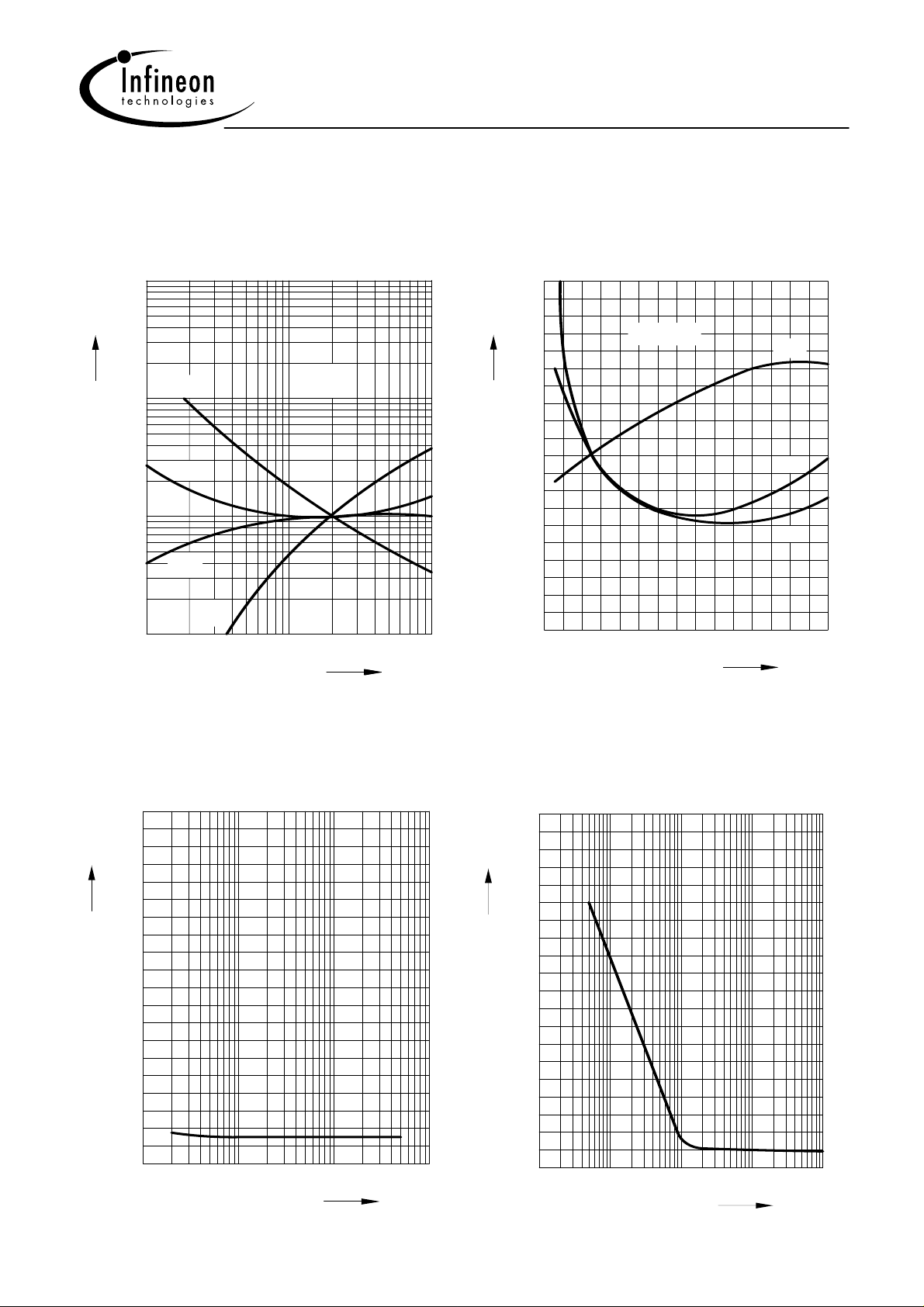
BC856...BC860
)
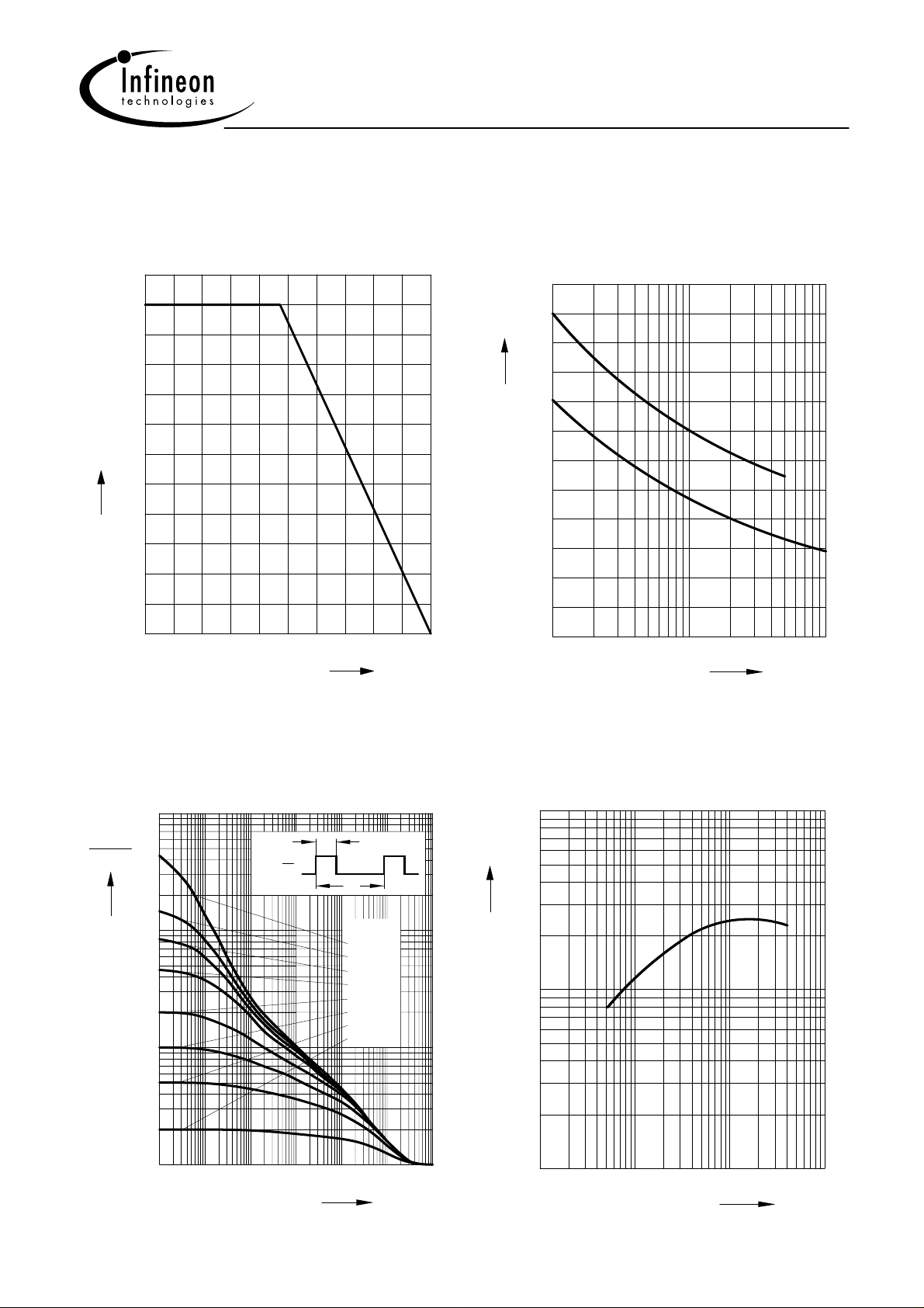
Total power dissipation P
360
mW
300
270
240
tot
P
210
180
150
120
90
60
30
0
0 15 30 45 60 75 90 105 120
= f(TS)
tot
°C
T
Collector-base capacitance C
Emitter-base capacitance CEB = f (V
BC 856...860
12
pF
C
CB0
(
)
C
EB0
CB
= f (V
EBO
EHP00376
CBO
)
10
8
C
EBO
6
4
C
CBO
2
150
S
0
-1 0 1
10
5
10 10
V
CB0
V
(
)
V
EB0
Permissible pulse load
P
totmax
P
totmax
totPDC
10
10
10
10
/ P
3
5
2
5
1
5
0
10
= f (tp)
totDC
=
D
-6
10-510-410-310
Transition frequency fT = f (IC)
V
= 5V
CE
EHP00378
mA
Ι
C
f
T
10
MHz
3
5
EHP00377
t
p
t
p
T
T
D
=
0
0.005
0.01
0.02
0.05
10
2
0.1
0.2
-2
0.5
0
10
s
t
p
5
1
10
-1 0 1 2
10 10 10 10
5
5
5 Jan-28-2005
BC856...BC860
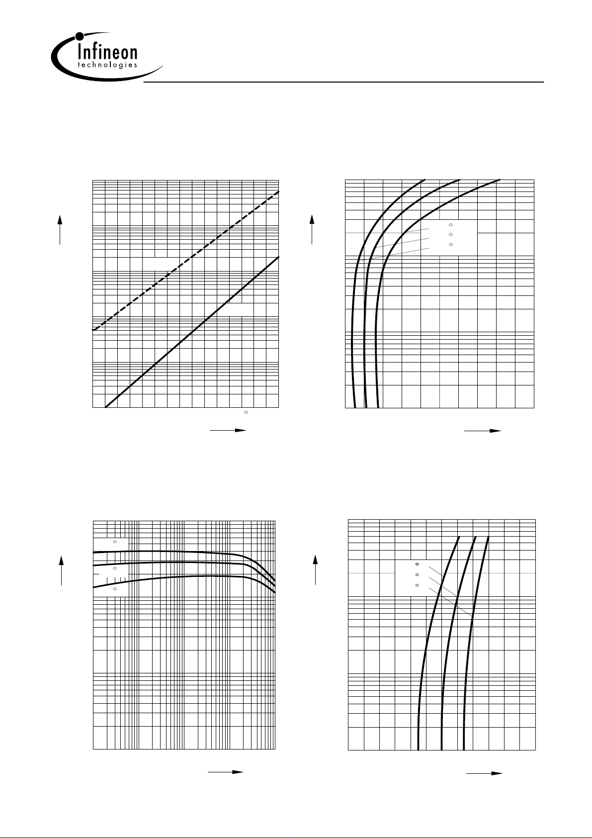
Collector cutoff current I
V
= 30V
CB
4
10
nA
Ι
CB0
3
10
5
2
10
5
1
10
5
0
10
5
-1
10
0 50 100 150
max
CBO
= f (TA)
EHP00381
typ
C
T
Collector-emitter saturation voltage
I
= f (V
C
2
10
mA
Ι
C
1
10
5
0
10
5
-1
10
0
A
), hFE = 20
CEsat
100
25
-50
0.1 0.2 0.4
EHP00380
C
C
C
0.3 0.5
V
V
CEsat
DC current gain hFE = f (IC)
V
= 5V
CE
3
10
5
100
h
FE
2
10
5
1
10
5
0
10
10 10 10 10
C
25
C
-50
C
-2
-1
555
10
0
Base-emitter saturation voltage
I
= f (V
C
EHP00382
Ι
C
12
mA
Ι
C
10
10
mA
10
5
10
5
-1
2
1
0
0
), hFE = 20
BEsat
C
100
C
C
25
-50
C
0.2 0.4 0.8
EHP00379
0.6 V 1.2
V
BEsat
6 Jan-28-2005
BC856...BC860
h parameter he = f (IC) normalized
V
= 5V
CE
BC 856...860 EHP00383
2
10
5
h
e
V
= 5 V
h
11e
1
10
5
h
12e
0
10
5
10
h
21e
h
-1
-1 0 1
10 10 10
22e
5
CE
mA
Ι
h parameter h
I
= 2mA
C
BC 856...860 EHP00384
2.0
h
e
= f (VCE) normalized
e
= 2 mA
Ι
C
h
11
1.5
1.0
0.5
0
0102030
C
h
12
h
22
V
V
CE
Noise figure F = f (VCE)
I
= 0.2mA, RS = 2kΩ, f = 1kHz
C
BC 856...860 EHP00385
20
dB
F
15
10
5
0
-1012
10 10 10 10
5 5
Noise figure F = f (f)
I
= 0.2mA, VCE = 5V, RS = 2kΩ
C
BC 856...860 EHP00386
20
dB
F
15
10
5
0
V
V
CE
-2 -1 1 2
10 10 10 10
10
0
kHz
f
7 Jan-28-2005
BC856...BC860
Noise figure F = f (IC)
V
= 5V, f = 120Hz
CE
BC 856...860 EHP00387
20
dB
F
15
= 1 M
R
S
10
5
0
-3 -2 0 1
10 10 10 10
100 k 10 k
Ω
ΩΩ
1 k
Ω
-1
10
500
mA
Ι
C
Noise figure F = f (I
V
= 5V, f = 1kHz
CE
BC 856...860 EHP00388
20
)
C
dB
F
15
R
= 1 M
S
100 k
ΩΩ
10 k
Ω
10
Ω
1 k
Ω
5
Ω
500
0
-3 -2 0 1
10 10 10 10
10
-1
mA
Ι
C
Noise figure F = f (IC)
V
= 5V, f = 10kHz
CE
BC 856...860 EHP00389
20
dB
F
15
10
5
0
10 10 10 10
500
Ω
Ω
1 k
-3 -2 0 1
= 1 MR
10
Ω
-1
S
100 k
10 k
mA
Ι
C
Ω
Ω
8 Jan-28-2005

Package Outline
0.4
Package SOT23
1.1 MAX.
MAX.
˚
2.6 MAX.
10
2
˚
...
0.1 MAX.
0.08...0.15
30
˚
±0.1
MAX.
1.3
˚
10
±0.1
2.9
A
1
+0.1
-0.05
1.9
B
3
2
0.95
+0.2
acc. to
DIN 6784
C
Foot Print
Marking Layout
0.25MBC
0.8
1.2
0.8
Manufacturer
Date code (Year/Month)
0.91.10.9
0.20
M
A
2003, July
Pin 1
Type code
Packing
Code E6327: Reel ø180 mm = 3.000 Pieces/Reel
Code E6433: Reel ø330 mm = 10.000 Pieces/Reel
4
0.9
Pin 1
3.15
2.13
BCW66
Example
0.2
8
2.65
1.15

Impressum
Published by Infineon Technologies AG,
St.-Martin-Strasse 53,
81669 München
© Infineon Technologies AG 2005.
All Rights Reserved.
Attention please!
The information herein is given to describe certain components and shall not be
considered as a guarantee of characteristics.
Terms of delivery and rights to technical change reserved.
We hereby disclaim any and all warranties, including but not limited to warranties of
non-infringement, regarding circuits, descriptions and charts stated herein.
Information
For further information on technology, delivery terms and conditions and prices
please contact your nearest Infineon Technologies Office (www.Infineon.com).
Warnings
Due to technical requirements components may contain dangerous substances.
For information on the types in question please contact your nearest Infineon
Technologies Office.
Infineon Technologies Components may only be used in life-support devices or
systems with the express written approval of Infineon Technologies, if a failure of
such components can reasonably be expected to cause the failure of that life-support
device or system, or to affect the safety or effectiveness of that device or system.
Life support devices or systems are intended to be implanted in the human body, or
to support and/or maintain and sustain and/or protect human life. If they fail, it is
reasonable to assume that the health of the user or other persons may be endangered.
 Loading...