ICS307
Serially Programmable Clock Source
Description
The ICS307-01 and ICS307-02 are versatile
serially programmable clock sources which take
up very little board space.
They can generate any frequency from 6 to
200 MHz, and have a second configurable
output. The outputs can be reprogrammed on
the fly, and will lock to a new frequency in 10 ms
or less. Smooth transitions (in which the clock
duty cycle remains roughly 50%) are guaranteed
if the output divider is not changed.
The devices include a PDTS pin which tri-states
the output clocks and powers down the entire
chip.
The ICS307-02 features a default clock output
at start-up and is recommended for all new
designs.
Features
• Packaged as 16 pin narrow SOIC
• Highly accurate frequency generation
• Serially programmable: user determines
the output frequency via a 3 wire interface.
• Eliminates need for custom quartz
• Input crystal frequency of 5 - 27 MHz
• Output clock frequencies up to 200 MHz
• Power Down Tri-State mode
• Very low jitter
• Operating voltages of 3.0 to 5.5 V
• 25 mA drive capability at TTL levels
• Industrial temperature available
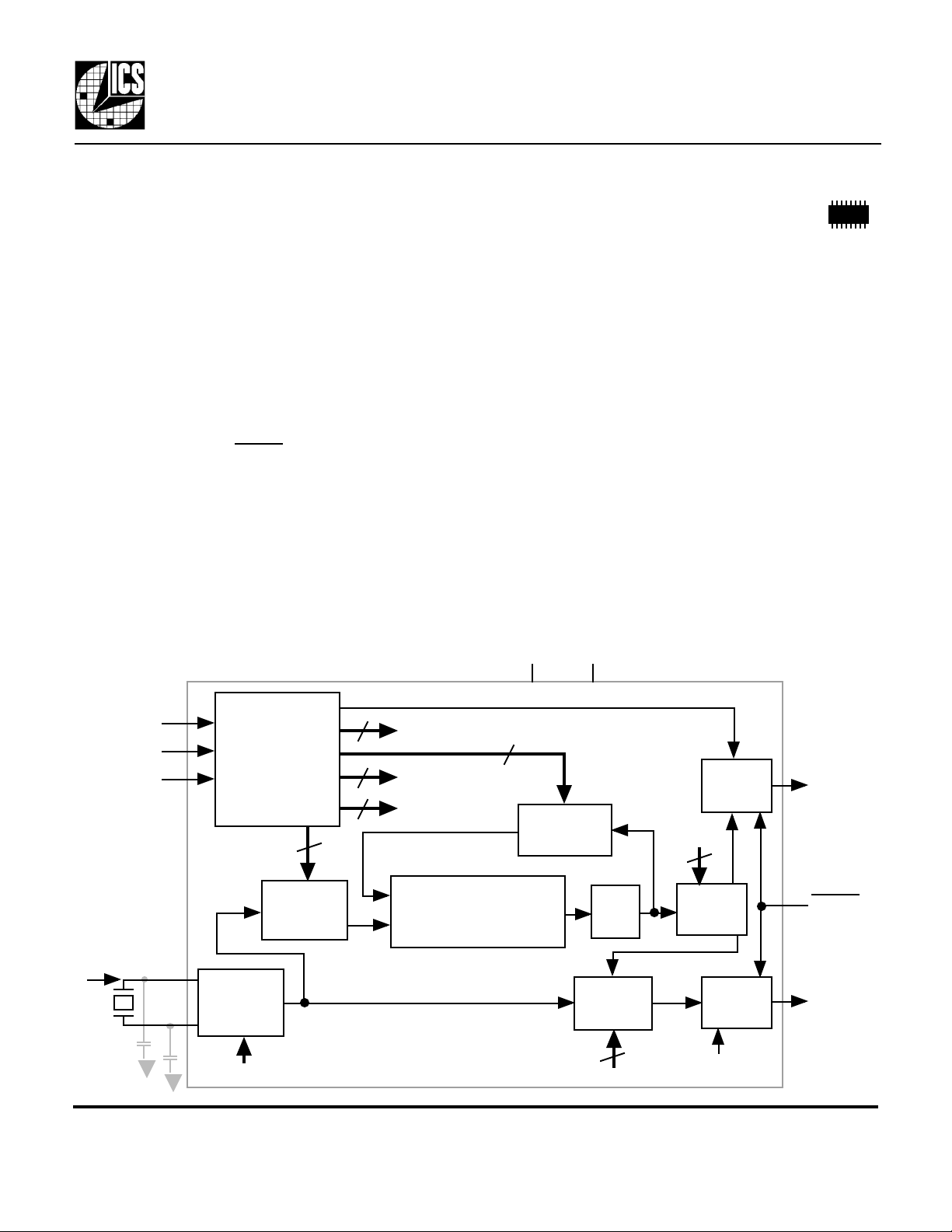
Block Diagram
SCLK
DATA
STROBE
Crystal or
clock input
X1/ICLK
X2
Shift
Register
R6:R0
Crystal
Oscillator
C1:C0
Reference
Divider
VDD GND
TTL
2
C1:C0
3
2
7
S2:S0
F1:F0
Phase Comparator,
Charge Pump,
and Loop Filter
9
V8:V0
VCO
Divider
Function
VCO
Select
2
F1:F0
Output
S2:S0
3
Output
Divider
Output
TTL
Buffer
Buffer
CLK1
PDTS
CLK2
MDS 307 D 1 Revision 042501
Integrated Circuit Systems, Inc. • 525 Race Street • San Jose •CA•95126•(408) 295-9800tel •www.icst.com

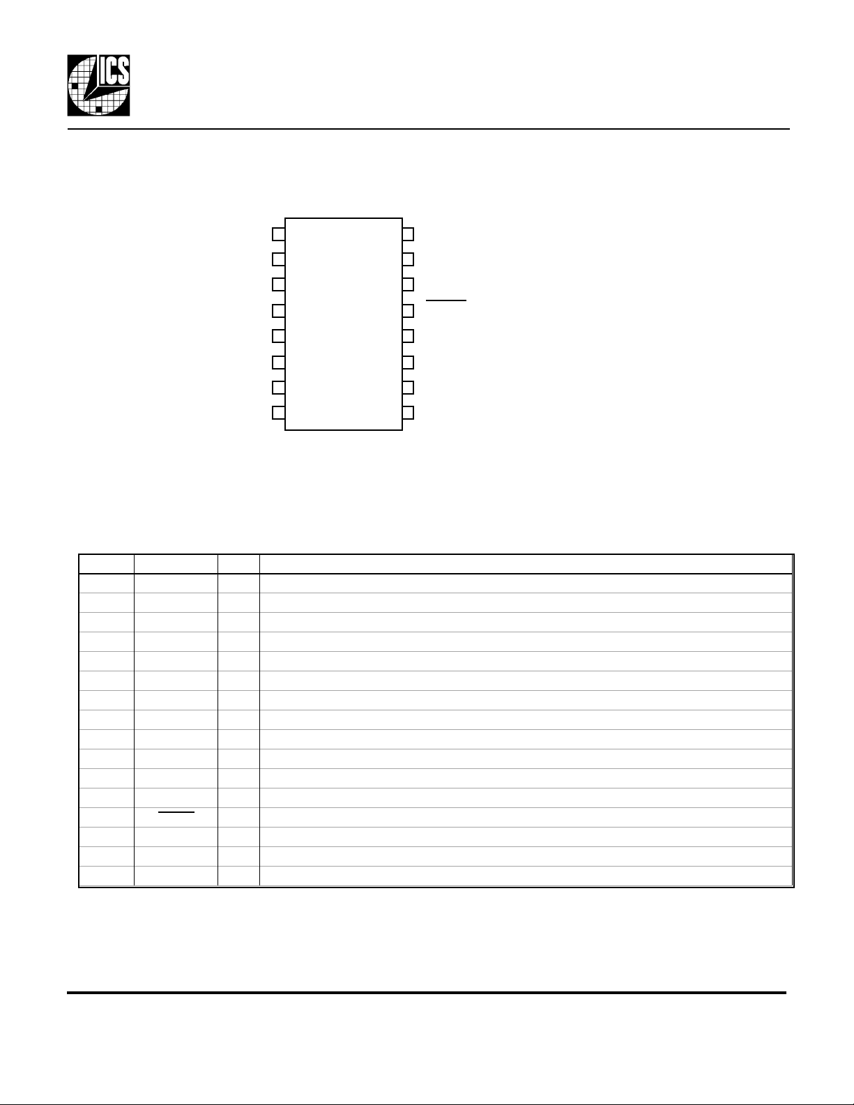
Pin Assignment
ICS307
Serially Programmable Clock Source
ICS307
X1/ICLK
NC
VDD
NC
GND
CLK2
NC
SCLK STROBE
1
2
3
4
5
6
7
8
16
15
14
13
12
11
10
X2
NC
NC
PDTS
DATA
CLK1
NC
9
16 pin Narrow
(0.150”) SOIC
Pin Description
Number Name Type Description
1 X1/ICLK XI Crystal connection (REF frequency). Connect to a parallel resonant crystal, or an input clock .
2 NC - No Connect.
3 VDD P Connect to +3.3V or +5V.
4 NC - No Connect.
5 GND P Connect to ground.
6 CLK2 O Output clock 2, determined by F0-F1. Can be reference, ref/2, CLK1/2 or off.
7 NC - No Connect.
8 SCLK I Serial clock. See timing diagram.
9 STROBE I Strobe to load data. See timing diagram.
10 NC - No Connect.
11 CLK1 O Output clock 1, determined by R0-R6, V0-V8, S0-S2 and input frequency.
12 DATA I Data Input. Serial input for three words which set the output clock(s).
13 PDTS I Powers down entire chip, tri-states CLK1 and CLK2 outputs, when low. Internal pull-up.
14 NC - No Connect.
15 NC - No Connect.
16 X2 XO Input crystal connection. Connect to a crystal, or leave unconnected for clock input.
Type: XI, XO=crystal connections, I = Input, O = output, P = power supply connection
MDS 307 D 2 Revision 042501
Integrated Circuit Systems, Inc. • 525 Race Street • San Jose •CA•95126•(408) 295-9800tel •www.icst.com

ICS307
Serially Programmable Clock Source
Determining the Output Frequency
On power-up the ICS307-01 on-chip registers can have random values, so almost any frequency may be
output from the part. CLK1 will always have some clock signal present, but CLK2 could possibly be OFF
(low).
The ICS307-02 on-chip registers are initially configured to provide a x1 output clock on both the CLK1
and CLK2 outputs. The output frequency will be the same as the input clock or crystal. This is useful if
the ICS307 will provide the initial system clock at power-up. Since this feature is an advantage in most
systems, the ICS307-02 is recommended for new designs.
With programming, the user has full control in changing the desired output frequency to any value over the
range shown in Table 1 on page 4. The output of the ICS307 can be determined by the following simple
equation:
CLK1 frequency = Input frequency • 2 •
Where VCO Divider Word (VDW) = 4 to 511 (0, 1, 2, 3 are not permitted)
Reference Divider Word (RDW) = 1 to 127 (0 is not permitted)
Output Divider = values on page 4
Also, the following operating ranges should be observed:
55 MHz < Input frequency • 2 •
200 kHz <
To determine the best combination of VCO, reference, and output dividers, contact ICS application
engineering. You may also fax this page to ICS at 408 295 9818(fax). Be sure to indicate the following:
Your Name ________________ Company Name___________________ Telephone_________________
Input Frequency
(RDW+2)
(VDW+8)
(RDW+2)
(VDW+8)
(RDW+2)(OD)
< 400 MHz
Commercial temperature range.
Industrial temperature limits are
60 MHz to 360 MHz.
Respond by e-mail (list your e-mail address) __________________or fax number ___________________
Desired input crystal_______ or clock_______ (in MHz) Desired output frequency_______________
REF Output_______VDD = 3.3V or 5V _______ Duty Cycle: 40-60% _____ or 45-55% required____
MDS 307 D 3 Revision 042501
Integrated Circuit Systems, Inc. • 525 Race Street • San Jose •CA•95126•(408) 295-9800tel •www.icst.com
 Loading...