Icom iC-r20 Service Manual

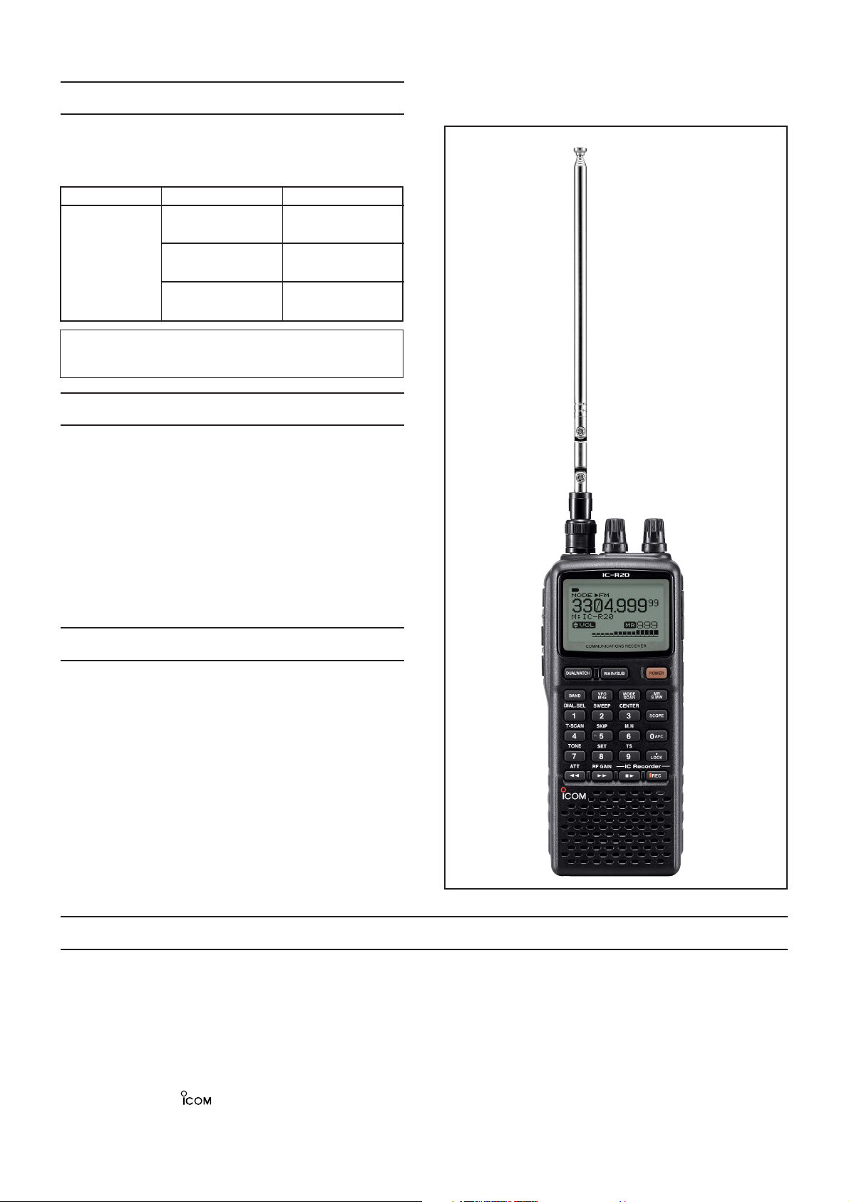
COMMUNICATIONS RECEIVER
iC-r20
SERVICE
MANUAL
INTRODUCTION
DANGER
This service manual describes the latest service information
for the IC-R20 COMMUNICATIONS RECEIVER at the time
of publication.
This service manual covers each versions.
MODEL
IC-R20
VERSION
[USA], [EXP-01],
[CAN]
[EUR], [EXP-02]
[UK], [SEA]
AC adapter
BC-149A
BC-149D
–
ORDERING PARTS
Be sure to include the following four points when ordering
replacement parts:
1. 10-digit order numbers
2. Component part number and name
3. Equipment model name and unit name
4. Quantity required
<SAMPLE ORDER>
1110003200 S.IC TA31136FN IC-R20 RF UNIT 5 pieces
8930062430 Key 2699 Keyboard IC-R20 Chassis 12 pieces
Addresses are provided on the inside back cover for your
convenience.
NEVER connect the receiver to an AC outlet or to an external DC power supply that uses more than 6.3 V. This will ruin
the receiver.
DO NOT expose the receiver to rain, snow or any liquids.
DO NOT reverse the polarities of the power supply when
connecting the receiver.
DO NOT apply an RF signal of more than 20 dBm (100 mW)
to the antenna connector. This could damage the receiver’s
front end.
REPAIR NOTES
1. Make sure a problem is internal before disassembling the receiver.
2. DO NOT open the receiver until the receiver is disconnected from its power source.
3. DO NOT force any of the variable components. Turn them slowly and smoothly.
4. DO NOT short any circuits or electronic parts. An insulated turning tool MUST be used for all adjustments.
5. DO NOT keep power ON for a long time when the receiver is defective.
6. READ the instructions of test equipment thoroughly before connecting equipment to the receiver.
To upgrade quality, any electrical or mechanical parts and
internal circuits are subject to change without notice or
obligation.
Icom, Icom Inc. and are registered trademarks of Icom Incorporated (Japan) in the United States, the United Kingdom,
Germany, France, Spain, Russia and/or other countries.

SECTION 1 SPECIFICATIONS
SECTION 2 INSIDE VIEWS
SECTION 3 DISASSEMBLY INSTRUCTIONS
SECTION 4 CIRCUIT DESCRIPTION
4-1 RECEIVER CIRCUITS . . . . . . . . . . . . . . . . . . . . . . . . . . . . . . . . . . . . . . . . . . . 4 - 1
4-2 PLL CIRCUITS . . . . . . . . . . . . . . . . . . . . . . . . . . . . . . . . . . . . . . . . . . . . . . . . . 4 - 7
4-3 OTHER CIRCUITS . . . . . . . . . . . . . . . . . . . . . . . . . . . . . . . . . . . . . . . . . . . . . 4 - 10
4-4 POWER SUPPLY CIRCUITS. . . . . . . . . . . . . . . . . . . . . . . . . . . . . . . . . . . . . . 4 - 11
4-5 PORT ALLOCATIONS. . . . . . . . . . . . . . . . . . . . . . . . . . . . . . . . . . . . . . . . . . . 4 - 12
4-6 BC-156 CIRCUIT DESCRIPTION . . . . . . . . . . . . . . . . . . . . . . . . . . . . . . . . . . 4 - 14
SECTION 5 ADJUSTMENT PROCEDURES
5-1 PREPARATION . . . . . . . . . . . . . . . . . . . . . . . . . . . . . . . . . . . . . . . . . . . . . . . . . 5 - 1
5-2 SOFTWARE ADJUSTMENTS . . . . . . . . . . . . . . . . . . . . . . . . . . . . . . . . . . . . . . 5 - 3
SECTION 6 PARTS LIST
SECTION 7 MECHANICAL PARTS AND DISASSEMBLY
SECTION 8 SEMI-CONDUCTOR INFORMATION
SECTION 9 BOARD LAYOUTS
9-1 RF UNIT. . . . . . . . . . . . . . . . . . . . . . . . . . . . . . . . . . . . . . . . . . . . . . . . . . . . . . 9 - 1
9-2 LOGIC UNIT. . . . . . . . . . . . . . . . . . . . . . . . . . . . . . . . . . . . . . . . . . . . . . . . . . . 9 - 3
9-3 REC UNIT . . . . . . . . . . . . . . . . . . . . . . . . . . . . . . . . . . . . . . . . . . . . . . . . . . . . 9 - 5
9-4 1STAVCO BOARD . . . . . . . . . . . . . . . . . . . . . . . . . . . . . . . . . . . . . . . . . . . . . . 9 - 7
9-5 1STBVCO BOARD . . . . . . . . . . . . . . . . . . . . . . . . . . . . . . . . . . . . . . . . . . . . . . 9 - 7
9-6 2NDCVCO BOARD. . . . . . . . . . . . . . . . . . . . . . . . . . . . . . . . . . . . . . . . . . . . . . 9 - 7
9-7 2NDDVCO BOARD . . . . . . . . . . . . . . . . . . . . . . . . . . . . . . . . . . . . . . . . . . . . . . 9 - 7
9-8 DOWNCONV BOARD. . . . . . . . . . . . . . . . . . . . . . . . . . . . . . . . . . . . . . . . . . . . 9 - 7
SECTION 10 BLOCK DIAGRAM
SECTION 11 VOLTAGE DIAGRAM
11-1 RF UNIT . . . . . . . . . . . . . . . . . . . . . . . . . . . . . . . . . . . . . . . . . . . . . . . . . . . . 11 - 1
11-2 LOGIC UNIT . . . . . . . . . . . . . . . . . . . . . . . . . . . . . . . . . . . . . . . . . . . . . . . . . 11 - 3
11-3 REC UNIT. . . . . . . . . . . . . . . . . . . . . . . . . . . . . . . . . . . . . . . . . . . . . . . . . . . . 11 - 4
11-4 1STAVCO BOARD . . . . . . . . . . . . . . . . . . . . . . . . . . . . . . . . . . . . . . . . . . . . . 11 - 5
11-5 1STBVCO BOARD . . . . . . . . . . . . . . . . . . . . . . . . . . . . . . . . . . . . . . . . . . . . . 11 - 5
11-6 2NDCVCO BOARD. . . . . . . . . . . . . . . . . . . . . . . . . . . . . . . . . . . . . . . . . . . . . 11 - 6
11-7 2NDDVCO BOARD . . . . . . . . . . . . . . . . . . . . . . . . . . . . . . . . . . . . . . . . . . . . . 11 - 6
11-8 DOWNCONV BOARD . . . . . . . . . . . . . . . . . . . . . . . . . . . . . . . . . . . . . . . . . . . 11 - 7
SECTION 12 BC-156 BATTERY CHARGER UNIT
12-1 DISASSEMBLY INFORMATION . . . . . . . . . . . . . . . . . . . . . . . . . . . . . . . . . . . 12 - 1
12-2 BC-156 BLOCK DIAGRAM . . . . . . . . . . . . . . . . . . . . . . . . . . . . . . . . . . . . . . . 12 - 1
12-3 BC-156 VOLTAGE DIAGRAM . . . . . . . . . . . . . . . . . . . . . . . . . . . . . . . . . . . . . 12 - 2
12-4 BC-156 BOARD LAYOUTS . . . . . . . . . . . . . . . . . . . . . . . . . . . . . . . . . . . . . . . 12 - 3
TABLE OF CONTENTS
1 - 1
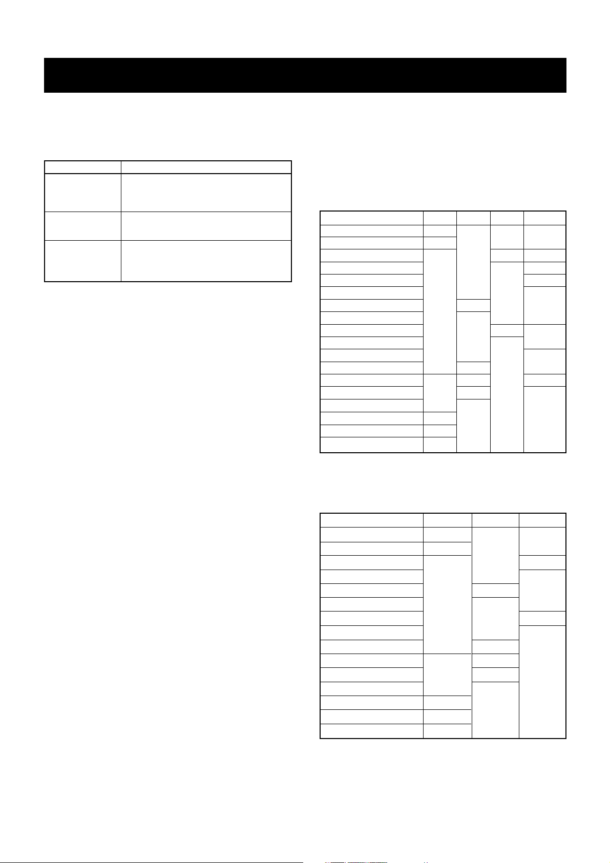
SECTION 1 SPECIFICATIONS
• IC-R20
M GENERAL
• Frequency coverage :
• Mode : FM, WFM, AM, SSB, CW
• No. of memory channel : 1250 channel
(incl. scan edge and auto
memory write ch.)
• Frequency stability : ±6 ppm max.
• Tuning steps : 0.01, 0.1, 1, 5, 6.25, 8.33*,
9*, 10, 12.5, 15, 20, 25,
30, 50 and 100 kHz
*selectable depending on
the operating frequency
band.
• Antenna Impedance : 50 Ω
• Power supply requirement :
3 × AA(R6) alkaline cells,
BP-206 or external power
supply (BC-149/A/D, CP-18)
• Polarity : Negative ground
• Current drain (at 3.7 V, backlight is OFF) :
Rated audio 150 mA typical
Standby 100 mA typical
Power saved 35 mA typical
(Power save ratio is 1 : 4)
• Usable temperature range : –10˚C to +60˚C
( –14˚F to +140˚F)
• Dimensions :
60(W) × 142(H) × 34.8(D) mm;
(projections not included)
23⁄8(W) × 519⁄32(H) ×13⁄8(D) in
•
Weight (with antenna and BP-206): Approx. 320 (g); 1119⁄32
(oz)
• External SP connector : 3-conductor 3.5(d) mm
(
1
⁄8”) / 8Ω
• Audio output power (at 3.7 V) : 100 mW typical at 10 %
distortion with an 8 Ω load
• BP-206 charging time : Approx. 8 hours
• Charging current : 400 mA typical
M RECEIVER
• Receiver system : Triple super heterodyne
and down convertor
• Intermediate frequency :
1st 266.7 and 429.1 MHz
2nd 19.65 MHz
3rd 450 kHz
• Sensitivity* :
Single mode receiving; Except spurious point (Unit; µV)
*
FM and WFM is measured at 12 dB SINAD. AM, SSB and
CW are measured at 10 dB S/N.
• Squelch Sensitivity : (except spurious points)
• Selectivity :
SSB/CW More than 1.8 kHz / –6 dB
AM / FM More than 12 kHz / –6 dB
Less than 30 kHz / –60 dB
WFM More than 150 kHz / –6 dB
All stated specifications are subject to change without notice or obligation.
Version
[EUR], [UK],
[SEA], [CAN]
[EXP-01], [EXP-02]
[USA]
[FRA]
Receive coverage (MHz)
0.150–3304.999
0.150–821.999, 851.000–866.999,
896.000–1304.999, 1305.000–3304.999
0.150–29.999, 50.200–51.200,
87.500–108.000, 144.000–146.000
430.000–440.000, 1240.000–1300.000
Frequency (MHz)
0.495 – 1.619
1.620 – 4.999
5.000 – 29.999
30.000 – 49.999
50.000 – 53.999
54.000 – 75.999
76.000 – 108.000
108.001 – 117.999
118.000 – 135.999
136.000 – 146.999
147.000 – 174.999
175.000 – 221.999
330.000 – 469.999
470.000 – 769.999
770.000 – 832.999
833.00 – 1304.999
1330.000 – 2304.999
2330.000 – 2999.999
FM
—
0.56
0.4
0.56
0.71
5.6
18
WFM
—
1.8
—
1.8
—
2.5
—
AM
2.2
1.4
—
1.4
—
SSB/CW
0.4
0.25
—
0.25
—
0.25
—
0.32
—
Frequency (MHz)
0.495 – 1.619
1.620 – 4.999
5.000 – 29.999
30.000 – 75.999
76.000 – 108.000
108.001 – 117.999
118.000 – 135.999
136.000 – 174.999
175.000 – 221.999
330.000 – 469.999
470.000 – 769.999
770.000 – 832.999
833.000 – 1304.999
1330.000 – 2304.999
2333.000 – 2999.999
FM
—
0.56 µV
0.4 µV
0.56 µV
0.71 µV
5.6 µV
18 µV
WFM
—
18 µV
—
18 µV
—
18 µV
—
AM
2.2 µV
1.4 µV
—
1.4 µV
—
1 - 2
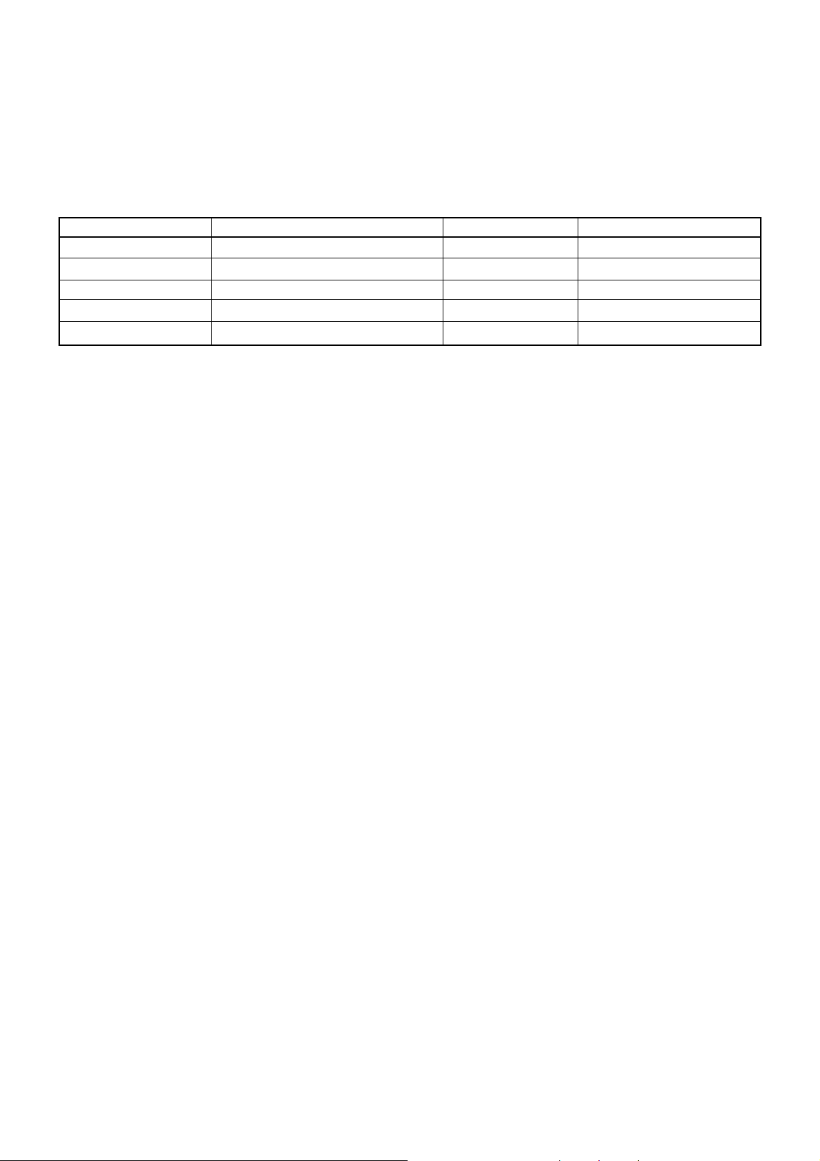
• BC-156
• Input voltage : 8.0–16.0 V
• Charging current : 0.96–1.44 A (Rapid charging)
• Usable temperature : 0˚C to +35˚C (+32˚F to +95˚F)
• Timer device : 192–288 minutes (Rapid charging)
12–18 minutes (Reserve charging)
• Protect function :
FUNCTION BP-206 CONDITION BC-156 ACTION LED CONDITION
Over discharge Becomes 1.5 V Charging stop Blinking orange
Over charge Becomes 4.5 V Charging stop Blinking orange
Overcurrent Shorten BP-206 and GND Charging stop Blinking orange
Full charge Becomes 4.2 V Charging stop Lighting green
Normal charging Becomes 3.5 V Charging Lighting orange
2 - 1
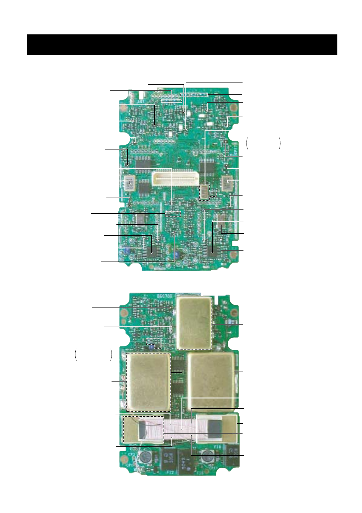
SECTION 2 INSIDE VIEWS
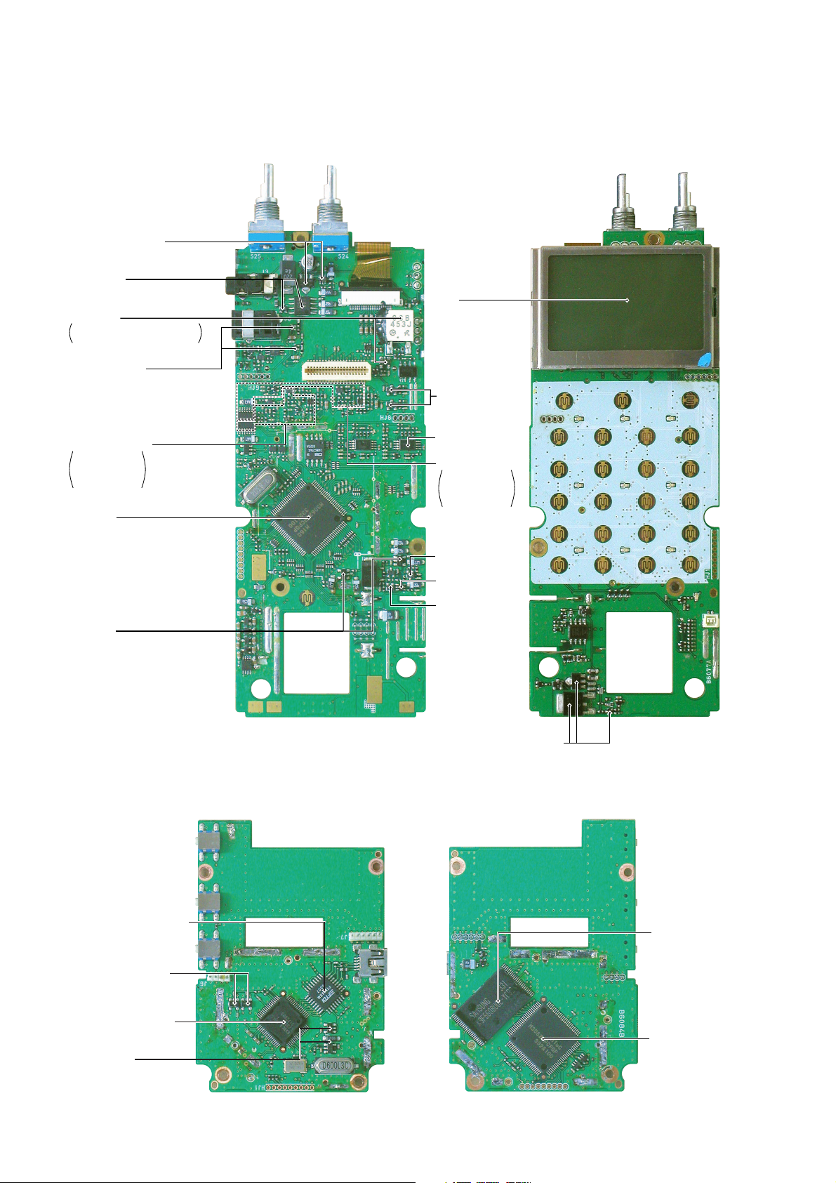
2-1 RF UNIT
• Top view
• Bottom view
Highpass filter circuit
(C854, C856, C858)
470—833 MHz
RF amplifier
(Q24: 2SC5008)
1G RF amplifier
(Q26: 2SC5624)
B-BAND RF amplifier
(IC18: PC2746TB)
B-BAND 1st mixer
(IC15: PC2757TB)
B-BAND 1st IF filter
(266.7 MHz)
(FI1: EFCH266MKQP1)
B-BAND 2nd mixer
(IC16: PC2757TB)
SSB AF amplifier
(Q532: 2SK1069)
SSB IF amplifier
450 kHz (Q531: 2SC4617)
BFO mixer
(D115, D116: RB876W)
B-BAND 3rd Lo amplifier
(Q555: 2SC5006)
B-BAND 2nd IF amplifier
(Q542: 2SC5006)
A-BAND IF IC
(IC2: TA31136FN)
A-BAND 2nd IF amplifier
(Q5: 2SC5006)
A-BAND 3rd Lo amplifier
(Q540: 2SC5006)
A-BAND 2nd IF filter
(19.65 MHz)
(FI3: FL-293)
A-BAND 2nd mixer
(IC10: PC2757TB)
A-BAND 1st IF filter
(429.1 MHz)
(FI4: EFCH429MKQP4)
A-BAND 1st mixer
(IC1: PC2757 TB)
A-BAND RF amplifier
(IC19: PC2757 TB)
30—300 MHz RF amplifier
(Q36: 2SC5006)
A-UHF RF amplifier
(Q35: 2SC5006)
B-UHF RF amplifier
(Q548: 2SC5006)
Lowpass filter circuit (L123—L125)
A/B-UHF (pre-amplifier (Q551: PA805T)
PLL reference oscillator circuit
Oscilktes 19.200 MHz
B-BAND FM IF IC
(IC17: TA31136FN)
X1: CR-593,
D171: HVC350B
Q556: 2SC4617
B-BAND
AM detector and AGC amplifier
(Q545: XP6501)
A-BAND AM detector
and AGC amplifier
(Q4: XP6501)
A/B-VHF
pre-amplifier
(Q550: FH102)
A-VHF A-band
RF amplifier
(Q14: 2SC5006)
MF/HF-L/HF-H
RF amplifier circuit
Q505: 2SC4226,
D163, D164:
MA2S728
B-BAND IF amplifier
(Q544: XP6501)
A-BAND IF amplifier
(Q1: XP6501)
DOWNCONV BOARD
1STBVCO BOARD
1STAVCO BOARD
Bar antenna
2NDDVCO BOARD
2NDCVCO BOARD
2 - 2
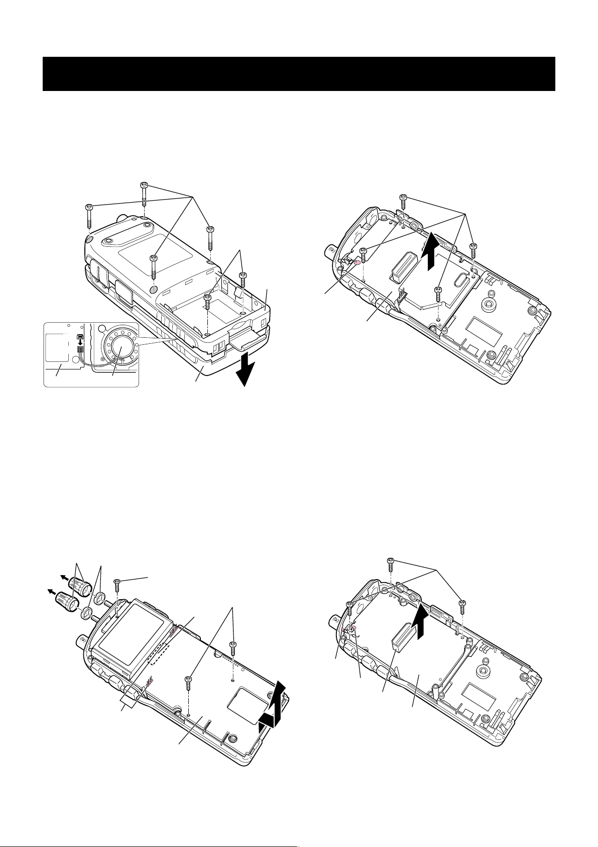
2-2 LOGIC UNIT
• Top view
• Bottom view
BFO circuit
IC6: SN74AHC1GU04DBVR
X2: CSBFB543K
AF amplifier regulator
(Q7: XP1501
Q9: 2SB1132)
AF amplifier
(IC15: TA31056F
Q8: 2SA1588)
AF pre-amplifiers
(Q12, Q16: 2SC4617)
+3 regulators
(Q10, Q15:
2SA1362)
Reset IC
(IC2: BD5228G)
Main CPU
(IC3: M30620MCP-129GP [OTHER],
M30620MCP-130GP [USA])
B-BAND AF circuit
Q24: XP6501,
Q27: 2SJ144,
Q22: 2SC4617,
IC7: SM6451B
A-BAND AF circuit
Q25: XP6501,
Q26: 2SJ144,
Q23: 2SC4617,
IC7: SM6451B
+3V reg.
(Q17: 2SA1588)
Battery daging regulators
(Q30: 2SB1201, Q32: 2SC4617, Q33: 2SB1132)
LCD
(DS12: M3-0243TIY)
+3SC reg.
(Q13: XP6501)
+3S reg.
(Q14: 2SA1588)
3V reg. IC
(IC8, IC9: R1111N321B)
Recording/playback IC
(IC7: ML2302TB)
+3V regulator
(IC1: BD5228G,
IC10: R1111N321B)
Mute (when SQL off)
(IC8, IC9:
SN74AHC1G66HDBVR)
USB interface IC
(IC3: FT245BM)
Sub CPU
(IC2: M30620FCPGP)
Flash memory for
recording/playback
(IC6: K9F5608UOC-YCBO)
2-3 REC UNIT
• Top view
• Bottom view
SECTION 3 DISASSEMBLY INSTRUCTIONS
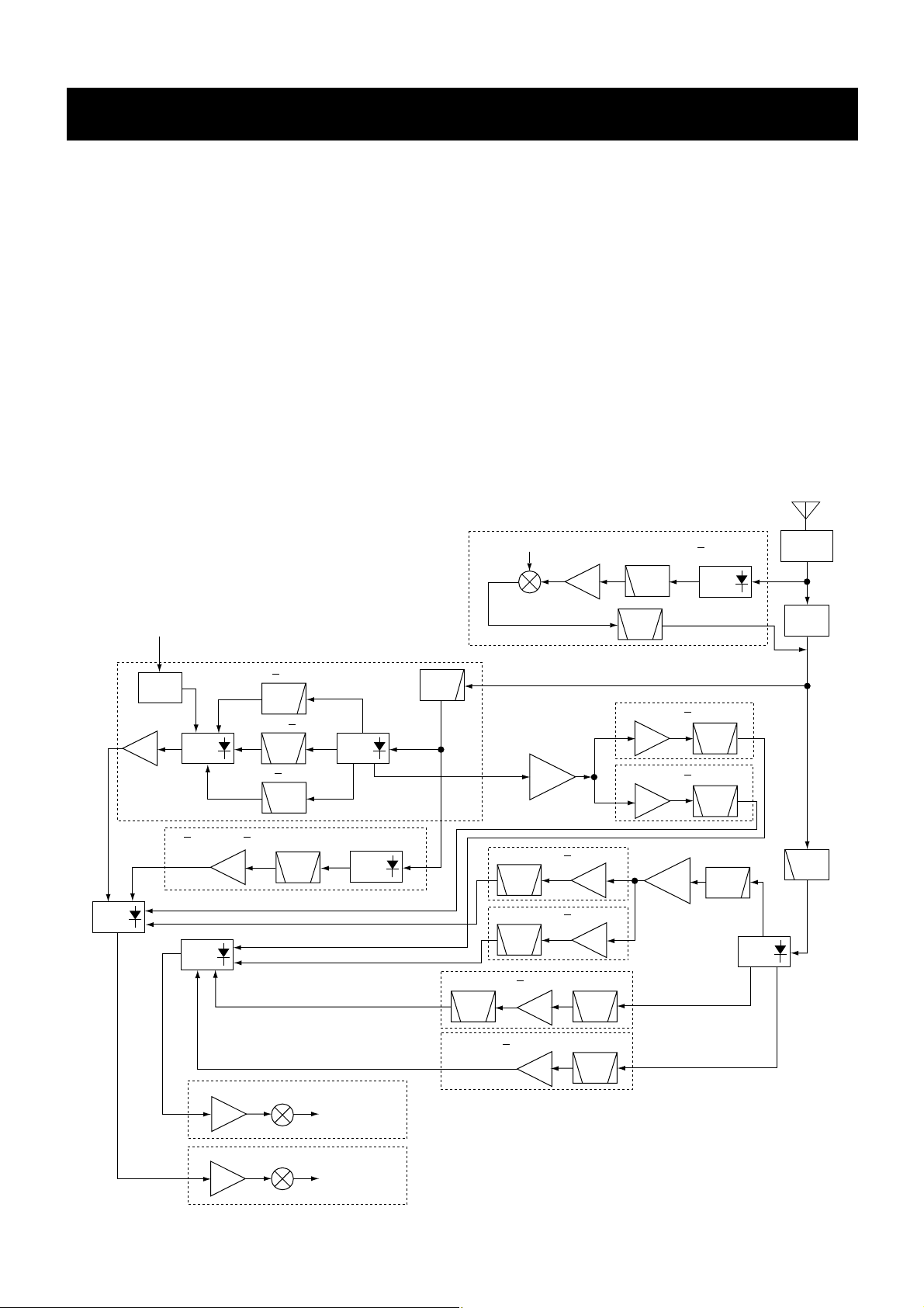
(1) REMOVING THE REAR PANEL
q Unscrew 4 screws, A (2 × 115 mm, black).
w Unscrew 2 screws, B (2 × 8 mm, black).
e Unplug W1 and J8 (LOGIC unit) to separate the front and
the rear panels.
(3) REMOVING THE REC UNIT
q Unscrew 4 flat-head screws, H (2 × 4 mm, silver).
w Unsolder 1 point, I.
e Remove the REC unit in the direction of the arrow.
(4) REMOVING THE RF UNIT
q Unscrew 3 flat-head screws, J (2 × 4 mm, silver).
w Unsolder 2 points, K.
e Remove the RF unit in the direction of the arrow.
Front panel
Rear panel
LOGIC unit
Speaker
W1
J8
A
B
H
I
REC unit
RF unit
J
K
K
J1
LOGIC unit
J5
C
D
E
F
G
(2) REMOVING THE LOGIC UNIT
q Remove 2 knobs, C, and unscrew 2 nuts, D.
w Unscrew 2 flat-head screws, E (2 × 4 mm, silver), and 1
pan-head screw, F (2 × 4 mm, black).
e Unsolder 10 points, G.
r Unplug J5 (bottom side of LOGIC unit) and J1 (RF unit) to
separate the LOGIC unit.
t Remove the LOGIC unit in the direction of the arrow.
3 - 1
4 - 1
4-1 RECEIVER CIRCUITS
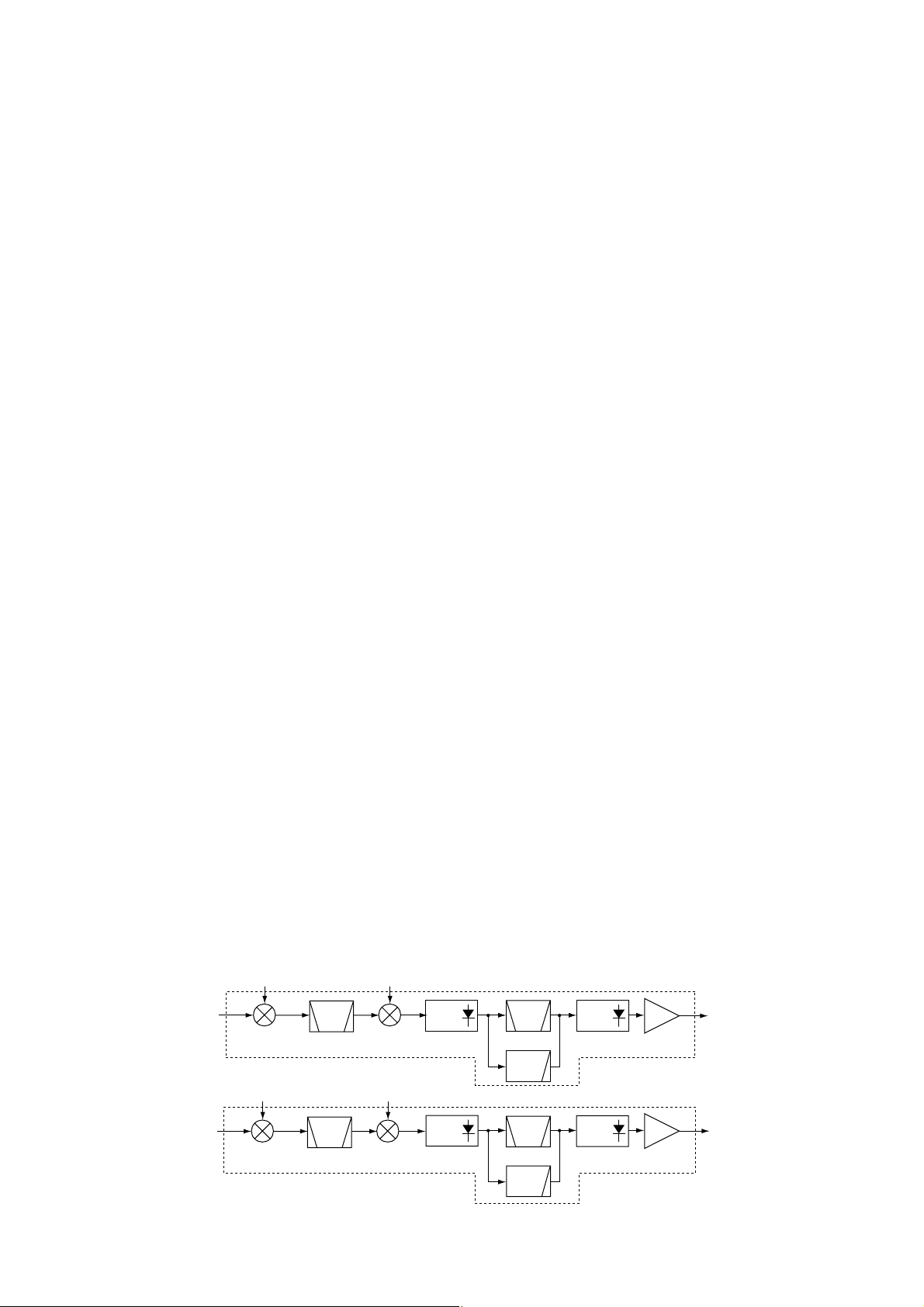
4-1-1 BAND SWITCHING CIRCUIT (RF UNIT)
The RF signals from the antenna connector pass through
the limiter (D68) and an attenuator* (D69). The signals are
then applied to the antenna switching circuit (D3, D11, D13,
D65, D66 and D73–D75 ).
*Above 2 GHz RF signals do not pass through the attenua-
tor.
4-1-2 RF CIRCUIT (RF UNIT)
The RF circuit amplifies the received signals within the
range of frequency coverage and filters out-of-band signals.
• A-BAND CIRCUIT
(1) MF (above 0.15 MHz, below 1.9 MHz) signals
RF signals (0.15–1.9 MHz) from an attenuator (D69) pass
through the low-pass filter (L123–L125 and C851–C853),
band switch (D66) and another low-pass filter (L88, L89,
C533–C535, C657, C658). The filtered signals pass through
another band switch (D67), and are then amplified at an RF
amplifier (Q505). The amplified signals are applied to the
next band switch (D72).
(2) HF-L (above 1.9 MHz, below 15 MHz) signals
RF signals (1.9–15 MHz) from an attenuator (D69) pass
through the low-pass filter (L123–L125 and C851–C853),
band switch (D65) and bandpass filter (L85–L87, L91,
C522–C531 and C891). The filtered signals pass through
another band switch (D70), and are then amplified at an RF
amplifier (Q505). The amplified signals are applied to the
next band switch (D72).
SECTION 4 CIRCUIT DESCRIPTION
RF
RF
BPF
BPF
BPF
RF
BPF
BPF
Pre
Amp
Pre
Amp
HF-L (1.9 15 MHz)
MF (15 30 MHz)
A-VHF (118 175 MHz)
B-VHF (118 175 MHz)
30 300M (30 300 MHz except A-VHF range)
A-UHF (300 470 MHz)
800M (470 833 MHz)
1G (833 1305 MHz)
B-UHF (300 470 MHz)
MF (0.15 1.9 MHz)
from the
bar antenna
HPF
HPF
LPF
LPF
LPF
LIMITER
BAND
SW
BAND
SW
BAND
SW
BAND
SW
BAND
SW
BAND
SW
BAND
SW
ANTENNA
ATT
ANT
SW
to 2nd mixer
circuit
RF-A circuit
RF-B circuit
1st mixer
1st mixer
to 2nd mixer
circuit
LO (1001 or 2002MHz)
RF
IC2IC3
mixer
1305 3305 MHz
RF
RF
BPF
RF
BPF
RF
BPF
RF
RF
RF
BPF
BPF
HPF
Q505
Q36
Q550
Q14
Q549
Q551
Q35
Q548
Q24
Q25
IC18
IC15
IC1
IC19
• RF CIRCUITS

4 - 2
(3) HF-H (above 15 MHz, below 30 MHz) signals
RF signals (15–30 MHz) from an attenuator (D69) pass
through the low-pass filter (L123–L125 and C851–C853),
band switch (D73) and bandpass filter (L81–L84 and
C511–C520). The filtered signals pass through another
band switch (D64), and are then amplified at an RF amplifier (Q505). The amplified signals are applied to the next
band switch (D72).
(4) A-VHF (above 118 MHz, below 175 MHz) signals
RF signals (118–175 MHz) from an attenuator (D69) pass
through the low-pass filter (L123–L125 and C851–C853),
band switch (D74), and are then applied to the pre-amplifier
(Q550) which is controlled by “A_VHF3V” signal via the
D148. The signals are amplified at the RF amplifier (Q14),
and pass through the bandpass filter (D1, D2, L1 and
C14–C16). The filtered signals are applied to the next band
switch (D25).
(5) 30–300M (above 30 MHz, below 300 MHz and except
A-VHF signals) signals
RF signals (118–175 MHz) from an attenuator (D69) pass
through the low-pass filter (L123–L125 and C851–C853)
and band switch (D75). The filtered signals pass through the
bandpass filter (L9, L10, L92, L133, C40–C43, C665 and
C666), and are then amplified at an RF amplifier (Q36). The
amplified signals are applied to the next band switch (D34).
(6) A-UHF (above 300 MHz, below 470 MHz) signals
RF signals (300–470 MHz) from an attenuator (D69) pass
through the high-pass filter (L126, L127 and C854–C858)
and band switch (D3). The filtered signals pass through the
low-pass filter (L3, L4, C22, C23 and C218), and are then
amplified at the pre-amplifier (Q551) which is controlled by
“A_UHF3V” signal via the D150. The amplified signals are
applied to the RF amplifier (Q35), and then pass through the
bandpass filter (D4, D5, L60, C58 and C59). The signals are
applied to the next band switch (D29).
• B-BAND CIRCUIT
(1) B-VHF (above 118 MHz, below 175 MHz) signals
RF signals (118–175 MHz) from an attenuator (D69) pass
through the low-pass filter (L123–L125 and C851–C853),
band switch (D74), and are then applied to the pre-amplifier
(Q550) which is controlled by “B_VHF3V” signal via the
D149. The signals are amplified at the RF amplifier (Q549),
and pass through the bandpass filter (D145, D146, L120,
C833 and C834). The filtered signals are applied to the next
band switch (D147).
(2) B-UHF (above 330 MHz, below 470 MHz) signals
RF signals (330–470 MHz) from an attenuator (D69) pass
through the high-pass filter (L126, L127 and C854–C858)
and band switch (D3). The filtered signals pass through the
low-pass filter (L3, L4, C22 and C23), and are then amplified
at the pre-amplifier (Q551) which is controlled by
“A_VHF3V” signal via the D151. The amplified signals are
applied to the RF amplifier (Q548), and then pass through
the bandpass filter (D141, D142, L113, C814 and C816).
The signals are applied to the next band switch (D143).
(3) 800M (above 470 MHz, below 833 MHz) signals
RF signals (470–833 MHz) from an attenuator (D69) pass
through the high-pass filter (L126, L127 and C854–C858)
and band switch (D11). The filtered signals pass through the
bandpass filter (D173, D174, L129 and L130), and are then
amplified at the RF amplifier (Q24). The amplified signals
pass through the bandpass filter (D175, D176 and L132).
The signals are applied to the next band switch (D32).
(4) 1G (above 833 MHz, below 1305 MHz) signals
RF signals (833–1305 MHz) from an attenuator (D69) pass
through the high-pass filter (L126, L127 and C854–C858)
and band switch (D13). The filtered signals pass through the
bandpass filter (L11–L13, L43, C5, C45–C51), and are then
amplified at the RF amplifier (Q26). The signals are applied
to the next band switch (D36).
4-1-3 DOWN CONVERTER CIRCUIT
(RF UNIT AND DOWNCONV BOARD)
The down converter circuit converts the signals within
1305–3305 MHz into 0.15 MHz to 1305 MHz signals.
The converted frequencies can calculate as follow.
F(x)=X–1001 (X is above 1305 MHz, below 2306 MHz)
F(x)=X–2002 (X is above 2306 MHz, below 3305 MHz)
NOTE: F(x) is converted frequency
X is receiving frequency
(Calculate example)
• Convert into 599 MHz when receiving 1600 MHz.
• Convert into 798 MHz when receiving 2800 MHz.
The RF signals from the limiter (D68) are applied to the
DOWNCONV board via the J1, pin 8 on the DOWNCONV
board. The signals pass through the band switch (DOWNCONV board; D1) and high-pass filter (DOWNCONV board;
L1, L2, C2–C4, C41 and C42), and are then amplified at the
RF amplifier (DOWNCONV board; IC2, pin 1). The signals
are mixed with 1001 MHz or 2002 MHz LO signal at the
mixer (DOWNCONV board; IC3, pin 1). The converted signals output from pin 6, and pass through the band switch
(DOWNCONV board; D2).
The converted signals are applied to the RF unit via J1,
pin 1 on the board. According to converted frequency, the
signals are applied to the each matched RF circuit.
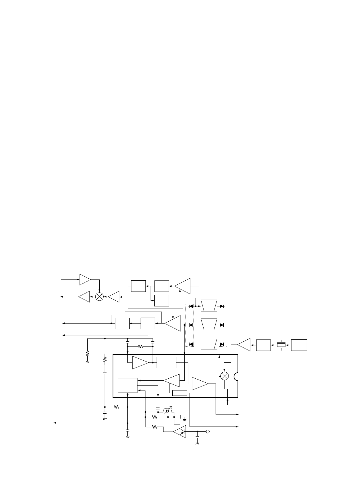
4-1-4 1ST MIXER AND 1ST IF CIRCUITS (RF UNIT)
The 1st mixer circuit converts the received RF signals to a
fixed frequency of the 1st IF signal with a PLL output frequency. By changing the PLL frequency, only the desired
frequency will pass through the bandpass filters at the next
stage of the 1st mixer.
• A-BAND CIRCUIT
The RF signals from the band switch (D25, D29, D34 and
D72) are amplified at the RF amplifier (IC19, pins 1, 4), and
are mixed with 1st LO signals at the 1st mixer circuit (IC1,
pin 1) to produce a 429.1 MHz 1st IF signal. The 1st IF signal is output from pin 6, and passed through the bandpass
filter (FI4) to suppress unwanted harmonic components. The
filtered 1st IF signal is applied to the 2nd mixer circuit.
The 1st LO signals are generated at the 1st A_VCO circuit
and are applied to the 1st mixer (IC1, pin 3) directly.
4 - 3
• B-BAND CIRCUIT
The RF signals from the band switch (D32, D36, D143 and
D147) are amplified at the RF amplifier (IC18, pins 1, 4), and
are mixed with 1st LO signals at the 1st mixer circuit (IC15,
pin 1) to produce a 266.7 MHz 1st IF signal. The 1st IF signal is output from pin 6, and passed through the bandpass
filter (FI1) to suppress unwanted harmonic components. The
filtered 1st IF signal is applied to the 2nd mixer circuit.
The 1st LO signals are generated at the 1st B_VCO circuit
and are applied to the 1st mixer (IC15, pin 3) directly.
4-1-5 2ND MIXER AND 2ND IF CIRCUITS (RF UNIT)
The 2nd mixer circuit converts the 1st IF signal to a 2nd IF
signal.
• A-BAND CIRCUIT
The filtered 429.1 MHz 1st IF signal from the bandpass filter
(FI4) is mixed with the 2nd LO signal at the 2nd mixer circuit
(IC10, pin 1, 6) to produce a 19.65 MHz 2nd IF signal.
In case of AM/CW/SSB/Narrow FM mode, the 2nd IF signal
passes through the mode switch (D58), crystal bandpass filter (FI3) and another mode switch (D60).
In case of WFM mode, the 2nd IF signal passes through the
mode switch (D59), low-pass filter (C202, C745, R207 and
R536) and another mode switch (D61).
The filtered 2nd IF signal is amplified at the 2nd IF amplifier
(Q5), and is then applied to the demodulator circuit.
• B-BAND CIRCUIT
The filtered 266.7 MHz 1st IF signal from the bandpass filter
(FI1) is mixed with the 2nd LO signal at the 2nd mixer circuit
(IC16, pin 1, 6) to produce a 19.65 MHz 2nd IF signal.
In case of AM/CW/SSB/Narrow FM mode, the 2nd IF signal
passes through the mode switch (D130), crystal bandpass
filter (FI7) and another mode switch (D132).
In case of WFM mode, the 2nd IF signal passes through the
mode switch (D131), low-pass filter (C755, C756, R428,
R429 and R537) and another mode switch (D133).
The filtered 2nd IF signal is amplified at the 2nd IF amplifier
(Q542), and is then applied to the demodulator circuit.
4-1-6 3RD MIXER AND DEMODULATOR CIRCUITS
(RF UNIT)
The 3rd mixer circuit converts the 2nd IF signal to a 3rd IF
signal. The demodulator circuit converts the 3rd IF signal
into AF signals.
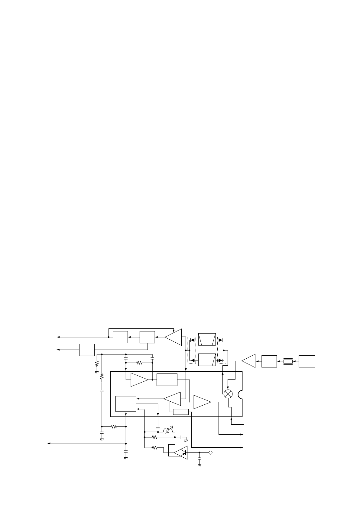
• A-BAND CIRCUIT
The 19.65 MHz 2nd IF signal from the 2nd IF amplifier (Q5)
is applied to the 3rd mixer section of the FM IF IC (IC2, pin
16) and is then mixed with the 3rd LO signal for conversion
into a 450 kHz 3rd IF signal.
IC2 contains the 3rd mixer, limiter amplifier, quadrature
detector and S-meter detector, etc. A frequency from the
PLL reference oscillator is used for the 3rd LO signal (19.20
MHz).
(1) FM MODE
The 3rd IF signal is output from the FM IF IC (IC2, pin 3),
and passes through the mode switch (D109) and ceramic
bandpass filter (FI2). The filtered signal passes through the
mode switch (D112), and is then fed back and amplified at
the limiter amplifier section (pin 5). The signal is demodulated to AF signals at the quadrature detector section (pins 10,
11) and detector coil (L21). The demodulated AF signals are
output from pin 9 and are applied to the AF switch (IC12, pin
11) via the “A_DETFM” line, and are then applied to the AF
circuit (LOGIC unit) as “A_DET” signal.
(2) WFM MODE
The 3rd IF signal is output from the FM IF IC (IC2, pin 3),
and passes through the mode switch (D108) and low-pass
filter (L99, C686 and C687). The filtered signal passes
through the mode switch (D111), and is then fed back to the
limiter amplifier section (pin 5). The amplified signal is
demodulated at the quadrature detector section (pins 10 and
11) and detector coil (L21). The AF signals are output from
pin 9 and are applied to the AF switch (IC12, pin 11) via the
“A_DETFM” line, and are then applied to the AF circuit
(LOGIC unit) as “A_DET” signal.
By connecting R55 to R54 in parallel, the output characteristics of pin 12, “RSSI”, change gradually. Therefore, the FM
IF IC can detect WFM components.
1st LO signal from
the 1STAVCO board
RF signals from
the A-BAND circuit
1st mixer
IC1
2nd mixer
IC10
2nd LO signal from
the 2NDCVCO board
2nd IF signal
A-BAND circuit
FI3
Q5
Q542
FI7
BPF
1st LO signal from
the 1STBVCO board
RF signals from
the B-BAND circuit
1st mixer
IC15
2nd mixer
IC16
2nd LO signal from
the 2NDDVCO board
BPF
B-BAND circuit
Xtal
BPF
LPF
BAND
SW
BAND
SW
RF
2nd IF signal
Xtal
BPF
LPF
BAND
SW
BAND
SW
RF
• 1ST, 2ND MIXER AND 2ND IF CIRCUITS
4 - 4
(3) AM MODE
The 3rd IF signal is output from the FM IF IC (IC2, pin 3),
and passes through the mode switch (D109) and ceramic
bandpass filter (FI2). The filtered signal passes through the
mode switch (D112), and is then applied to the IF amplifier
(Q531). The amplified signal is demodulated at the AM
detector (Q4). The AF signals pass through the ANL circuit
(D114), and are then applied to the AF switch (IC12, pin 4)
via the “A_DETAM” line, and are then applied to the AF circuit (LOGIC unit) as “A_DET” signal.
(4) SSB/CW MODES
The 3rd IF signal is output from the FM IF IC (IC2, pin 3),
and passes through the mode switch (D110) and ceramic
bandpass filter (FI6). The filtered signal passes through the
mode switch (D113), and is then applied to the IF amplifier
(Q531). The amplified signal is mixed with BFO signal from
the LOGIC unit at the mixer (D115 and D116) to demodulate
to AF signals. The AF signals are applied to the SSB AF
amplifier (Q532), and are then applied to the AF switch
(IC12, pin 1) via the “A_DETSSB” line, and are then applied
to the AF circuit (LOGIC unit) as “A_DET” signal.
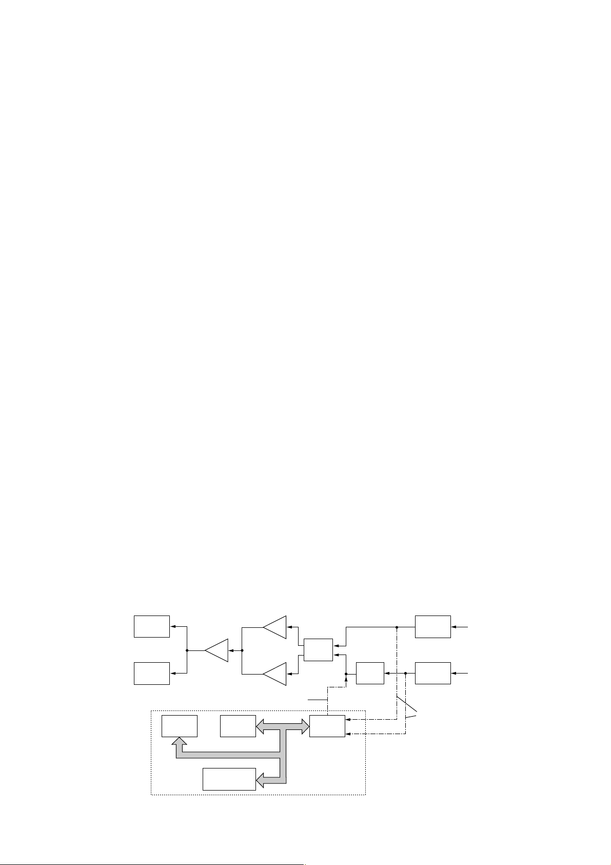
• B-BAND CIRCUIT
The 19.65 MHz 2nd IF signal from the 2nd IF amplifier
(Q542) is applied to the 3rd mixer section of the FM IF IC
(IC17, pin 16) and is then mixed with the 3rd LO signal for
conversion into a 450 kHz 3rd IF signal.
IC17 contains the 3rd mixer, limiter amplifier, quadrature
detector and S-meter detector, etc. A frequency from the
PLL reference oscillator is used for the 3rd LO signal (19.20
MHz).
(1) FM MODE
The 3rd IF signal is output from the FM IF IC (IC17, pin 3),
and passes through the mode switch (D134) and ceramic
bandpass filter (FI8). The filtered signal passes through the
mode switch (D136), and is then fed back and amplified at
the limiter amplifier section (pin 5). The signal is demodulated AF signals at the quadrature detector section (pins 10,
11) and detector coil (L105). The demodulated AF signals
are output from pin 9 and are applied to the AF switch (IC21,
pin 1) via the “DET_OUT” line, and are then applied to the
AF circuit (LOGIC unit) as “B_DET” signal.
(2) WFM MODE
The 3rd IF signal is output from the FM IF IC (IC17, pin 3),
and passes through the mode switch (D135) and low-pass
filter (L106, C781 and C782). The filtered signal passes
through the mode switch (D137), and is then fed back to the
limiter amplifier section (pin 5). The amplified signal is
demodulated at the quadrature detector section (pins 10 and
11) and detector coil (L105). The AF signals are output from
pin 9 and are applied to the AF switch (IC21, pin 1) via the
“DET_OUT” line, and are then applied to the AF circuit
(LOGIC unit) as “B_DET” signal.
By connecting R436 to R437 in parallel, the output characteristics of pin 12, “RSSI”, change gradually. Therefore, the
FM IF IC can detect WFM components.
16
Limiter
amp.
X1
19.2 MHz
Q540
Q556 D171
RSSI
IC2 TA31136F
13
2nd IF (19.65 MHz)
from Q5
"A_RSSI" signal to the CPU
(LOGIC unit; IC3, pin 91)
11
10
9
87
5
3
2
Active
filter
Noise
detector
FM
detector
Noise
comp.
"A_NOISE" signal to the CPU
(LOGIC unit; IC3, pin 5)
12
R54
R55
C101
C94
R56
C95
C98
C99
AM
DET
IF
C96
R61
R59
R60
"A_WFMC"
L21
C93
C242
"A_DETFM" signal
to the AF switch
"A_AGC" signal to
RF amplifiers
"A_DETSSB" signal
to the AF switch
"BFO" signal from
the LOGIC unit
Mixer
3rd
Q41
DET
NB
AGC
AGC
MUTE
SW
REF
CONT.
REF
OSC
LO
SSB/CW
FI6
LPF
AM/NFM
WFM
Q521,
Q525
Q523
Q524,
Q526,
Q528
Q522
Q1
AF
Q532
D115
D116
IF
Q531
Q530
Q4Q4
FI2
• A-BAND 3RD MIXER AND DEMODULATOR CIRCUITS
4 - 5
(3) AM MODE
The 3rd IF signal is output from the FM IF IC (IC17, pin 3),
and passes through the mode switch (D134) and ceramic
bandpass filter (FI8). The filtered signal passes through the
mode switch (D136), and is then applied to the IF amplifier
(Q544). The amplified signal is demodulated at the AM
detector (Q545). The AF signals pass through the ANL circuit (D139), and are then applied to the AF switch (IC21, pin
4) via the “AM_DET” line, and are then applied to the AF circuit (LOGIC unit) as “B_DET” signal.
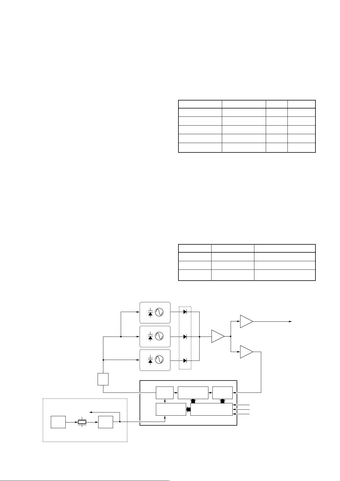
4-1-7 AF AMPLIFIER CIRCUIT (LOGIC UNIT)
The AF amplifier circuit amplifies the demodulated AF signals to drive a speaker.
• A-BAND CIRCUIT
While in FM mode, AF signals from the demodulator circuit
(RF unit) pass through the AF filter (Q25), and are then
amplified at the AF amplifier (Q23).
While in WFM/AM/SSB/CW modes, AF signals from the
demodulator circuit (RF unit) bypass the AF filter via the AF
filter bypass switch (Q26), and are then amplified at the AF
amplifier (Q23).
The signals are applied to the electronics volume (IC7, pin
6) to control volume level. The signals output from pin 5, and
are applied to the pre-amplifier (Q12). The signals are amplified at the AF amplifier (IC5, pin 1), and then output from pin
6. The signals are applied to the internal speaker which is
connected with J8 via the external speaker jack (J3).
• B-BAND CIRCUIT
While in FM mode, AF signals from the demodulator circuit
(RF unit) pass through the AF filter (Q24), and are then
amplified at the AF amplifier (Q22).
While in WFM/AM modes, AF signals from the demodulator
circuit (RF unit) bypass the AF filter via the AF filter bypass
switch (Q27), and are then amplified at the AF amplifier
(Q22).
The signals are applied to the electronics volume (IC7, pin
11) to control volume level after passing through the mute
switch (Q19). The signals output from pin 12, and are
applied to the pre-amplifier (Q16). The signals are amplified
at the AF amplifier (IC5, pin 1), and then output from pin 6.
The signals are applied to the internal speaker which is connected with J8 via the external speaker jack (J3).
The electronic volume control circuit controls AF gain, therefore, the AF output level is according to the [VOL] setting
and also the squelch conditions.
4-1-8 SQUELCH CIRCUIT (LOGIC AND RF UNITS)
• NOISE SQUELCH
The noise squelch circuit cuts out AF signals when no RF
signals are received. By detecting noise components in the
AF signals, the squelch circuit switches the AF mute switch.
A portion of the “A_NOISE” signals from the FM IF IC (RF
unit; IC2, pin 13) are applied to the CPU (LOGIC unit; IC3,
pin 5). The CPU analyzes the noise condition and outputs
the “AFON” signal (from pin 17) to the AF amplifier’s controller (LOGIC unit; Q7).
• TONE SQUELCH
The tone squelch circuit detects AF signals and opens the
squelch only when receiving a signal containing a matching
subaudible tone (CTCSS). When tone squelch is in use, and
a signal with a mismatched or no subaudible tone is
received, the tone squelch circuit mutes the AF signals even
when noise squelch is open.
16
Limiter
amp.
X1
19.2 MHz
Q555
Q556 D171
RSSI
IC2 TA31136F
13
2nd IF (19.65 MHz)
from Q5
"B_RSSI" signal to the CPU
(LOGIC unit; IC3, pin 87)
11
10
9
87
5
3
2
Active
filter
Noise
detector
FM
detector
Noise
comp.
"B_NOISE" signal to the CPU
(LOGIC unit; IC3, pin 4)
12
R437
R436
C765
C764
R443
C772
C768
C769
AM
DET
IF
C770
R440
R439
R438
"B_WFMC"
L105
C880
C767
"DET_OUT" signal
to the AF switch
"B_AGC" signal to
RF amplifiers
"AM_DET" signal
to the AF switch
Mixer
3rd
Q543
AGC
REF
CONT.
REF
OSC
LO
LPF
AM/NFM
WFM
FI8
Q544Q545Q545
ANL
D139
• B-BAND 3RD MIXER AND DEMODULATOR CIRCUITS
4 - 6
(1) A-BAND CIRCUIT
A portion of the AF signals from the FM IF IC (RF unit; IC2,
pin 9) passes through the low-pass filter (LOGIC unit; C161,
C164, R169 and R175) via the “A_DET” line to remove AF
(voice) signals and is applied to the CTCSS decoder inside
the CPU (LOGIC unit; IC3, pin 89) via the “A_CTONE” line
to control the AF mute switch.
(2) B-BAND CIRCUIT
A portion of the AF signals from the FM IF IC (RF unit; IC17,
pin 9) passes through the low-pass filter (LOGIC unit; C160,
C163, R168 and R174) via the “B_DET” line to remove AF
(voice) signals and is applied to the CTCSS decoder inside
the CPU (LOGIC unit; IC3, pin 90) via the “B_CTONE” line
to control the AF mute switch.
4-1-9 AGC CIRCUIT (RF UNIT)
The AGC (Automatic Gain Control) circuit reduces IF and
RF amplifiers gain to keep the audio output at a constant
level. The receiver gain is determined by the voltage on the
AGC line (A-BAND circuit is Q4’s collector, B-BAND circuit
is Q545’s collector).
• A-BAND CIRCUIT
A part of the 3rd IF signal from the mode switch
(D111–D113) is amplified at the IF amplifier (Q1), and is then
applied to the AM detector. (Q4, pin 5). The signal is output
from pin 1, and is then applied to the AGC circuit of the same
one (pin 3). The signal is output from pin 4 as “A-AGC” signal, and is then applied to the 3rd IF amplifier (Q1), 2nd IF
amplifier (Q5) and RF amplifiers (Q14, Q35, Q36 and
Q505).
• B-BAND CIRCUIT
A part of the 3rd IF signal from the mode switch (D136 and
D137) is amplified at the IF amplifier (Q544), and is then
applied to the AM detector. (Q545, pin 5). The signal is output from pin 1, and is then applied to the AGC circuit of the
same one (pin 3). The signal is output from pin 4 as “B-AGC”
signal, and is then applied to the 3rd IF amplifier (Q544), 2nd
IF amplifier (Q542) and RF amplifiers (Q24, Q25, Q548 and
Q549).
The A-AGC or B-AGC voltage is used for the the bias voltage of the IF and RF amplifiers. When receiving strong signals, the detected voltage increases and the AGC voltage
decreases. Therefore, the receiver obtain stable receiver
gain.
4-1-10 IC RECORDER CIRCUIT (LOGIC UNIT)
The IC RECORDER circuit is composed of RECORDER IC
(IC7), sub CPU (IC2), flash memory (IC6), USB interface
(IC3), etc.
(1) IN CASE OF RECORDING
• A-BAND CIRCUIT
The AF signals from the AF amplifier (Q23) are applied to
the REC board via the HJ8, pin 2 as “A_AIN” signal. The signals are applied to the RECORDING IC (IC7, pin 25) to compress the voice signals, and are then converted to digital signals. The signals are applied to the sub CPU (IC2), and are
then stored in the flash memory (IC6).
• B-BAND CIRCUIT
The AF signals from the AF amplifier (Q22) are applied to
the REC board via the HJ8, pin 3 as “B_AIN” signal. The signals pass through the AF mute switch (IC8, pins 1 and 2),
and are then applied to the RECORDING IC (IC7, pin 20) to
compress the voice signals, and are then converted to digital signals. The signals are applied to the sub CPU (IC2),
and are then stored in the flash memory (IC6).
(2) IN CASE OF PLAYBACK
The stored RECORDING data in the flash memory (IC6) are
applied to the sub CPU (IC2), and are then applied to the
RECORDING IC (IC7). The signals are converted to analog
signals, and are then expanded into the AF voice signals.
The AF signals output from RECORDING IC (IC7, pin 25).
The signals are applied to the LOGIC unit via the J6, pin 3
as “AOUT” signal, and are then applied to the electronics
volume (IC7, pin 11) to control volume level. The signals output from pin 12, and are applied to the pre-amplifier (Q16).
The signals are amplified at the AF amplifier (IC5, pin 1), and
then output from pin 6. The signals are applied to the internal speaker which is connected with J8 via the external
speaker jack (J3).
AF Filter
Amplifier
AF Filter
Amplifier
SW
VR
EXT. SP.
J3
Rec. IC
IC7
Memory
IC6
USB Interface
IC3
Sub CPU
IC2
INT. SP.
J8
A_DET
B_DET
Q23, Q25, Q26
Q22, Q24, Q27
Recoding line
Playing line
Q19
IC7
Pre. amp.
Q12
Pre. amp.
Q16
AF amp.
REC UNIT
IC5
• AF AMPLIFIER AND IC RECORDER CIRCUITS
4 - 7
4-2 PLL CIRCUITS
4-2-1 PLL CIRCUIT
A PLL circuit provides stable oscillation of the 1st LO frequencies. The PLL circuit compares the phase of the divided VCO frequency to the reference frequency. The PLL output frequency is controlled by the divided ratio (N-data) of a
programmable divider.
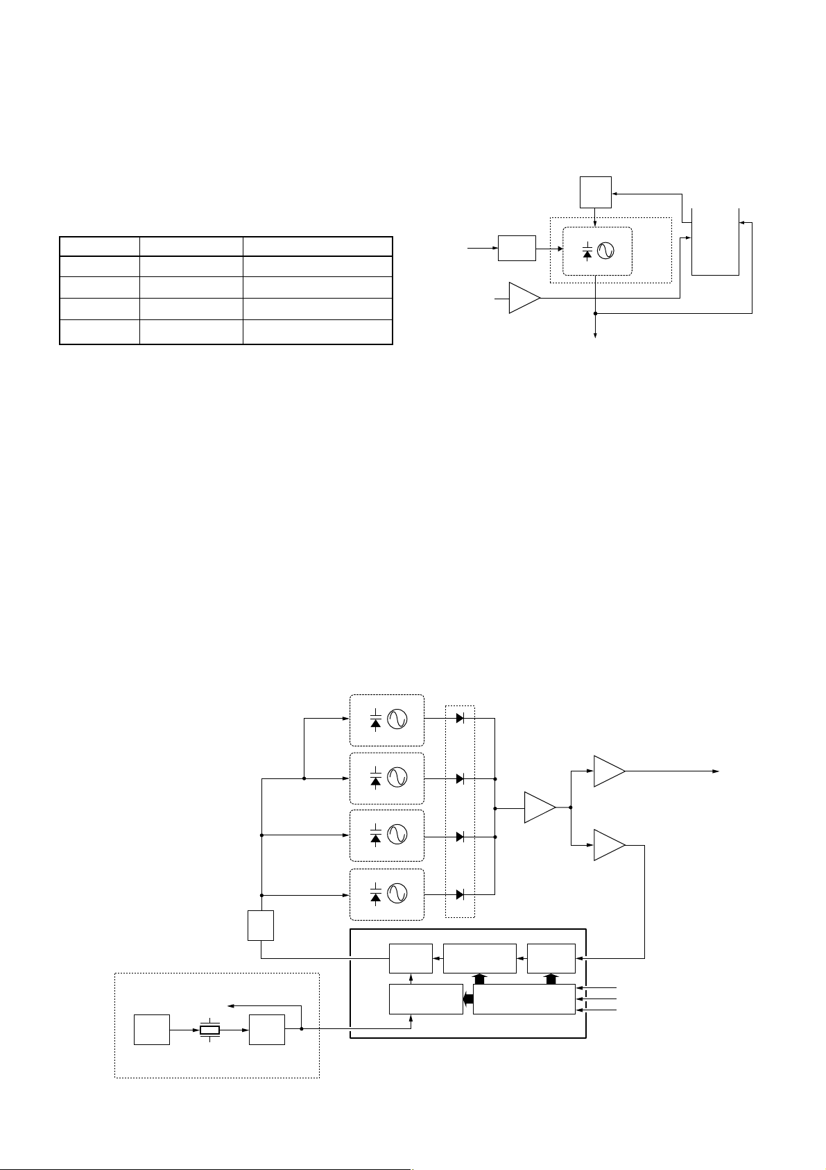
• A-BAND CIRCUIT (1STAVCO BOARD)
An oscillated signal from one of the 1st VCO circuits
(Q1–Q3, D1–D4) passes through the LO switch (D7–D19)
and buffer amplifiers (IC2, Q8). The amplified signal is
applied to the PLL IC (IC3, pin 11) and is prescaled in the
PLL IC based on the divided ratio (N-data). The PLL IC
detects the out-of-step phase using the reference frequency
and outputs it from pin 5. The output signal is passed
through the loop filter (Q6, Q7), and is then applied to the
one of the 1st VCO circuits as the lock voltage.
• B-BAND CIRCUIT (1STBVCO BOARD)
An oscillated signal from one of the 1st VCO circuits
(Q1–Q5, D1–D5) passes through the LO switch (D7–D10)
and buffer amplifiers (IC2, Q8). The amplified signal is
applied to the PLL IC (IC3, pin 11) and is prescaled in the
PLL IC based on the divided ratio (N-data). The PLL IC
detects the out-of-step phase using the reference frequency
and outputs it from pin 5. The output signal is passed
through the loop filter (Q6, Q7), and is then applied to the
one of the 1st VCO circuits as the lock voltage.
• DOWN CONVERTER PLL CIRCUIT
(DOWNCONV BOARD)
An oscillated signal from the VCO circuit (Q1, D3) is amplified at the buffer amplifier (Q2). The amplified signal is
applied to the PLL IC (IC4, pin 8) and is prescaled in the PLL
IC based on the divided ratio (N-data). The PLL IC detects
the out-of-step phase using the reference frequency and
outputs it from pin 5. The output signal is passed through the
low-pass filter (L6, C21, C22 and C40), and is then applied
to the one of the 1st VCO circuits as the lock voltage.
4-2-2 REFERENCE OSCILLATOR CIRCUIT
(RF UNIT)
The reference oscillator circuit (X1, Q556, D171) generates
a 19.2 MHz reference frequency which is stabilized within
the temperature range –10˚C (+14˚F) to +60˚C (+140˚F).
The reference frequency is applied to the PLL ICs (refer to
the list below in details) and the FM IF ICs (IC2, pin 2 for ABAND circuit: IC17, pin 2 for B-BAND circuit) via the LO
amplifiers (Q540 for A-BAND circuit; Q555 for B-BAND circuit).
4-2-3 1ST VCO CIRCUITS
(1STAVCO AND 1STBVCO BOARDS)
• A-BAND CIRCUIT (1STAVCO BOARD)
The oscillated signal at 1st A-VCO circuits is applied to the
buffer amplifiers (IC2) via one of the LO switches (D7–D9).
The amplified signal is applied to the 1st mixer circuit (RF
unit; IC1, pin 3) via the LO amplifier (Q9).
The 1st A-VCO circuit is composed of 1AVCO, 2AVCO and
3AVCO. Components and osillating frequences of each circuits are as follow list.
Shift register
Prescaler
Phase
detector
Loop
filter
REF.
OSC.
REF.
CONT.
Programmable
counter
Programmable
divider
X1
19.2 MHz
to the FM IF IC
RF UNIT
1AVCO
Buffer
Buffer
Buffer
LO
switch
Q9
Q8
IC2
16
17
18
PLLBSTB
IC3 (PLL IC)
PLLDATA
PLLCK
to the 1st mixer circuit
19
5
11
Q1, D1, D2
D7
D8
D9
2AVCO
Q2, D3
3AVCO
Q3, D4
Q6,
Q7
• A-BAND PLL CIRCUIT
BOARD NAME PLL IC INPUT OUTPUT
1STAVCO IC3 pin 19 pin 5
1STBVCO IC3 pin 19 pin 5
2NDCVCO IC1 pin 1 pin 6
2NDDVCO IC1 pin 1 pin 6
DOWNCONV IC4 pin 1 pin 5
1st A-VCO Components Oscillating freq. (MHz)
1AVCO Q1, D1 and D2 849.1–899.0999
2AVCO Q2 and D3 604.1–849.0999
3AVCO Q3 and D4 429.25–604.0999
4 - 8
A portion of the signal from the buffer amplifier (IC2) is
amplified at the buffer amplifier (Q8) and is then fed back to
the PLL IC (IC3, pin 11) as the comparison signal.
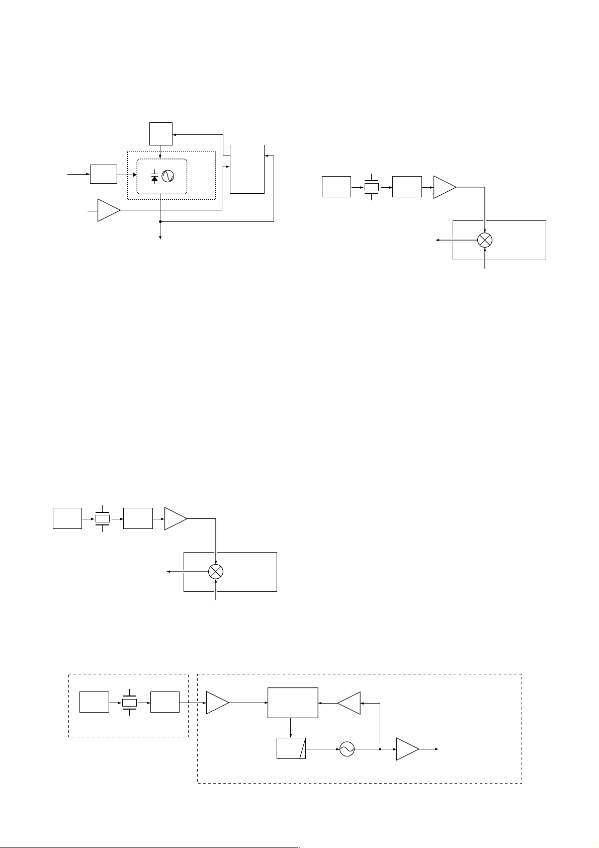
• B-BAND CIRCUIT (1STBVCO BOARD)
The oscillated signal at 1st B-VCO circuits is applied to the
buffer amplifiers (IC2) via one of the LO switches (D7–D10).
The amplified signal is applied to the 1st mixer circuit (RF
unit; IC15, pin 3) via the LO amplifier (Q9). Components and
osillating frequences of each circuits are as follow list.
A portion of the signal from the buffer amplifier (IC2) is
amplified at the buffer amplifier (Q8) and is then fed back to
the PLL IC (IC3, pin 11) as the comparison signal.
4-2-4 2ND VCO CIRCUITS
(2NDCVCO AND 2NDDVCO BOARDS)
The 2nd VCO circuit generates the 2nd LO frequencies, and
the signals are applied to the 2nd mixer circuit.
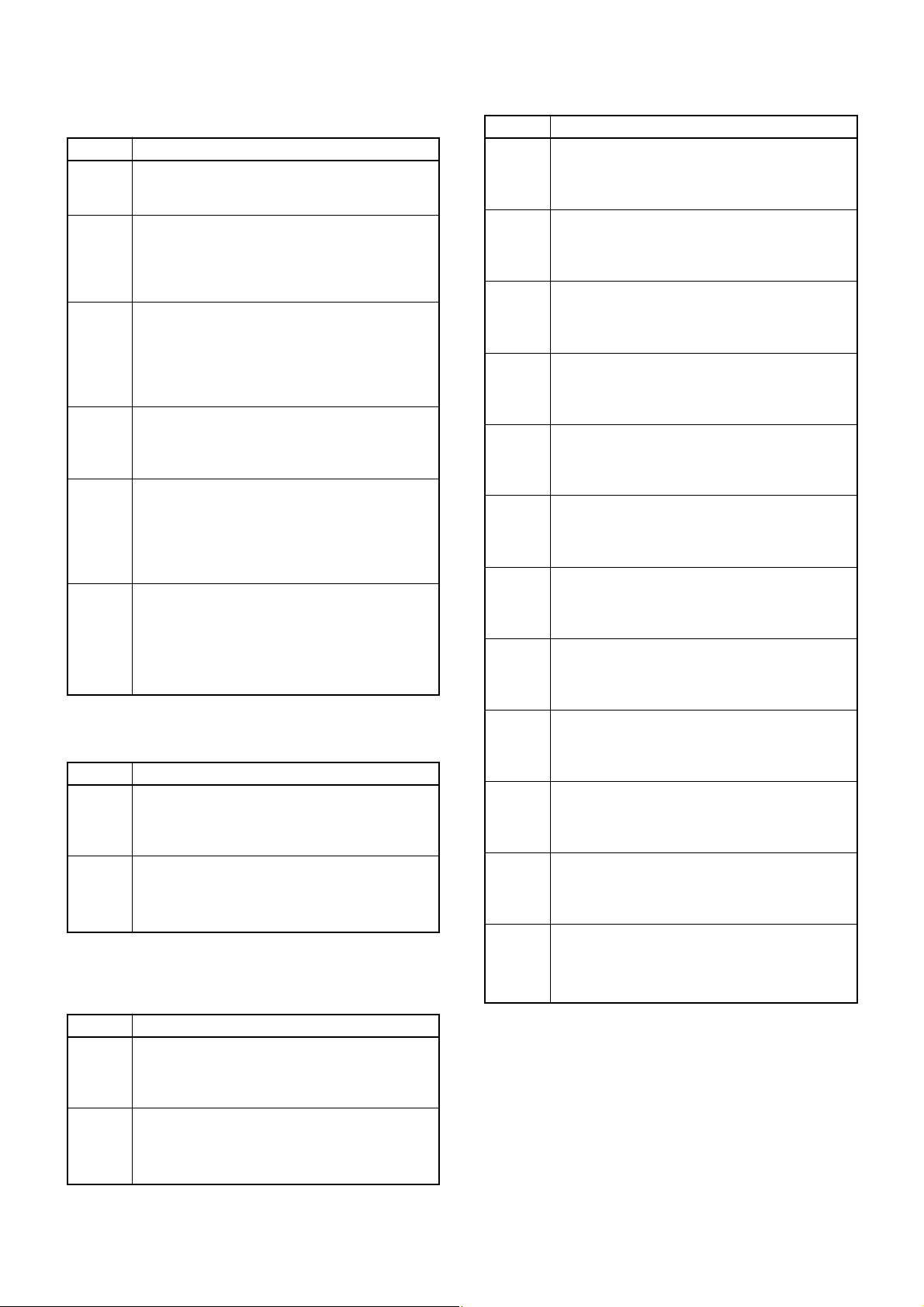
• A-BAND CIRCUIT (2NDCVCO BOARD)
The 2nd C-VCO circuit (Q1 and D1) generates 409.4500
MHz and 448.7500 MHz. The oscillated signal is applied to
the 2nd mixer (RF unit; IC10, pin 3), and is then mixed with
the 1st IF signal.
A part of oscillated signal from the 2nd C-VCO circuit is
applied to the PLL IC (IC1, pin 8) as the comparison signal,
and is then output from pin 5. The signal passes through the
loop filter (R14, R15 and R22), and is then applied to the 2nd
C-VCO circuit again as PLL lock voltage.
Shift register
Prescaler
Phase
detector
Loop
filter
REF.
OSC.
REF.
CONT.
Programmable
counter
Programmable
divider
X1
19.2 MHz
to the FM IF IC
RF UNIT
1BVCO
Buffer
Buffer
Buffer
LO
switch
Q9
Q8
IC2
16
17
18
PLLBSTB
IC3 (PLL IC)
PLLDATA
PLLCK
to the 1st mixer circuit
19
5
11
Q1, D1, D2
D7
D8
D9
D10
2BVCO
Q2, D3
3BVCO
Q3, D4
4BVCO
Q4, Q5, D5
Q6,
Q7
• B-BAND PLL CIRCUIT
• 2ND C VCO CIRCUIT
1st B-VCO Components Oscillating freq. (MHz)
1BVCO Q1, D1 and D2 863.3–1099.6999
2BVCO Q2 and D3 683.3–866.6999
3BVCO Q3 and D4 566.3–686.6999
4BVCO Q4, Q5 and D5 384.7–441.6999
A_R3V
OSC
(19.2 MHz)
Q4
Ripple
filter
Buffer
Q3
to the 2nd mixer (IC10, pin 3)
Loop
filter
VCO
Q1, D1
2ND
VCO
5
8
PLL IC
IC1
1
4 - 9
• B-BAND CIRCUIT (2NDDVCO BOARD)
The 2nd D-VCO circuit (Q1 and D1) generates 247.0500
MHz and 286.3500 MHz. The oscillated signal is applied to
the 2nd mixer (RF unit; IC16, pin 3), and is then mixed with
the 1st IF signal.
A part of oscillated signal from the 2nd C-VCO circuit is
applied to the PLL IC (IC1, pin 8) as the comparison signal,
and is then output from pin 5. The signal passes through the
loop filter (R14, R15 and R22), and is then applied to the 2nd
D-VCO circuit again as PLL lock voltage.
4-2-5 3RD LO CIRCUIT (RF UNIT)
The 3rd LO circuit uses 19.2 MHz reference signal which is
generates at the X1 and Q556.
• A-BAND CIRCUIT
The 19.2 MHz reference signal is amplified at the LO amplifier (Q540), and is then applied to the FM IF IC (IC2, pin 2)
as the 3rd LO signal.
The signal is mixed with 2nd IF signal to convert into 3rd IF
signal. The 3rd IF signal is applied to one of demodulator
(FM/WFM/AM/SSB) circuits.
• B-BAND CIRCUIT
The 19.2 MHz reference signal is amplified at the LO amplifier (Q555), and is then applied to the FM IF IC (IC17, pin 2)
as the 3rd LO signal.
The signal is mixed with 2nd IF signal to convert into 3rd IF
signal. The 3rd IF signal is applied to the each demodulator
(FM/WFM/AM) circuits.
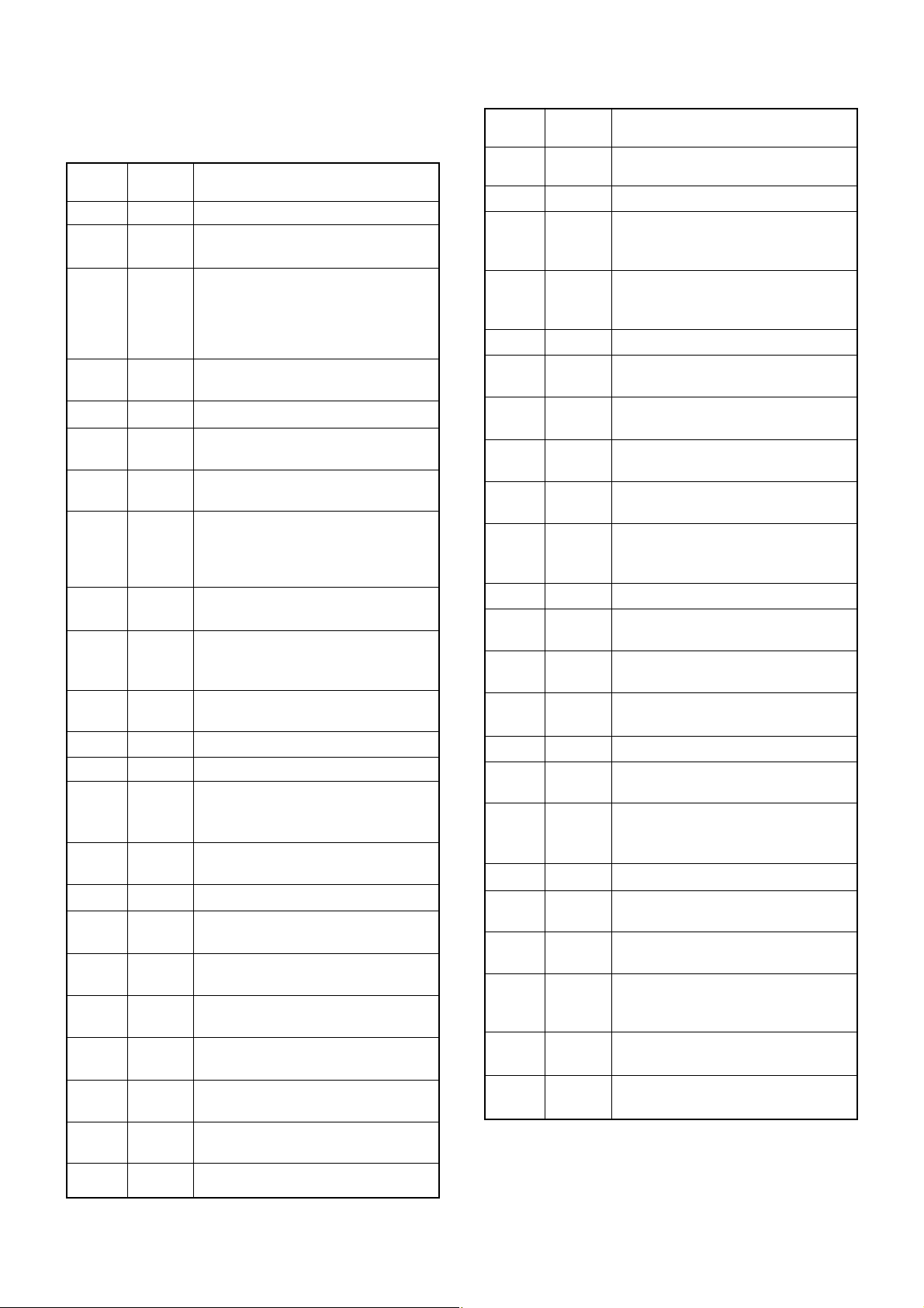
4-2-6 DOWN CONVERTER VCO CIRCUIT
(DOWNCONV BOARD)
The DOWN CONVERTER circuit uses 19.2 MHz reference
signal which is generates at the X1 and Q556 on the RF unit.
The DOWN CONVERTER VCO circuit (Q1 and D3) generates 1001 MHz or 2002 MHz. The oscillated signal is amplified at the buffer amplifier (Q4), and passes through band
switch.
When receiving 1305–2305.999 MHz RF signals, 1001 MHz
LO signal is selected. The RF signals pass through band
switch (D6), and then pass through another band switch
(D8).
When receiving 2306–3304.999 MHz, 2002 MHz LO signal
is selectd. The RF signals pass through the band switch
(D5), and then pass through the high-pass filter (L9, L10 and
C28–C32). The signals passes through another band switch
(D7).
The 1001 MHz or 2002 MHz LO signal is applied to the
mixer circuit (IC3, pin 3).
A part of oscillated signal from the DOWN CONVERTER
VCO circuit is amplified at the buffer amplifier (Q2), and is
then applied to the PLL IC (IC4, pin 8) as the comparison
signal, and is then output from pin 5. The signal passes
through the loop filter (L6, C21, C22 and C40), and is then
applied to the DOWN CONVERTER VCO circuit again as
PLL lock voltage.
• 2ND D VCO CIRCUIT
D171
X1
REF
CONT.
Q556
REF
OSC
Q540
19.2 MHz 3rd LO signal
3rd mixer
FM IF IC (IC2)
2nd IF signal
to the demodulator circuits
LO
• 3RD LO CIRCUIT (A-BAND)
D171
X1
REF
CONT.
Q556
REF
OSC
Q555
19.2 MHz 3rd LO signal
3rd mixer
FM IF IC (IC17)
2nd IF signal
to the demodulator circuits
LO
• 3RD LO CIRCUIT (B-BAND)
D171
X1
REF
CONT.
Q556
REF
OSC
LPF
Q6
DOWNCONV BOARD
RF UNIT
19.2 MHz
PLL IC
IC4
Buff
Q2
VCO
Q1, D3
Buff
Q4
1001 MHz or 2002 MHz
LO signal to the mixer (IC3)
Buff
• DOWN CONVERTER VCO CIRCUIT
A_R3V
OSC
(19.2 MHz)
Q4
Ripple
filter
Buffer
Q3
to the 2nd mixer (IC16, pin 3)
Loop
filter
VCO
Q1, D1
2ND
VCO
5
8
PLL IC
IC1
1

4 - 10
4-2-7 BFO CIRCUIT (LOGIC UNIT)
The oscillated signal at the BFO VCO circuit (IC6, X2) is
applied to the MAIN unit via the J5 (pin 35) as the BFO, and
is then amplified at the BFO amplifier (RF unit; Q530). The
amplified signal is mixed with 3rd IF signal to demodulate to
AF signal on SSB/CW modes.
The carrier frequency is shifted by “BFO_SHIFT” signal from
the main CPU (IC3, pin 2) while receiving SSB modes.
4-3 OTHER CIRCUITS
4-3-1 BATTERY CHARGER CIRCUIT (LOGIC UNIT)
When charging the installed battery (BP-206), the battery
charger control signal (CHGC) becomes high, and is then
output from the CPU (IC3, pin 39). The signal is applied to
the battery charger controller (Q34), and its output controls
the battery charger circuit (Q31, D28, D29) to output 400 mA
(typical) charging current.
4-3-2 BAR ANTENNA TUNING CIRCUIT (RF UNIT)
When selecting the internal bar antenna while AM band signals are receiving, the interal bar antenna switching signal is
output from the D/A converter (IC22, pin 7) as “ANTSW” signal. The signal is applied to the antenna switching circuit
(Q510, D76), and then switches to the internal bar antenna.
The expander IC (IC14) outputs the “A-TRAC” bar antenna
control signal from pin 8. The signal is applied to the level
converter (Q513), and is then applied to the AM bar antenna tune circuit (D100). The circuit tunes to the desire frequency to change the D100’s capacity.
4-3-3 EARPHONE ANTENNA CIRCUIT
(LOGIC AND RF UNITS)
When selecting the earphone antenna while WFM band
receiving, the received RF signal passes through the external speaker jack (LOGIC unit; J3). The signal is applied to
the RF unit via the J5, pin 4 as “EAR” signal. The signal is
applied to the antenna switch (RF unit; D101), and is then
applied to the 30–300 MHz RF circuit.
4-3-4 RESET CIRCUIT (LOGIC UNIT)
When [POWER] switch is ON, CPU3 signal from the +3 regulator (IC8) is applied to the reset IC (IC2, pin 2). The IC outputs reset signal via the “RESET” line, and the signal is
applied to the main CPU (IC3, pin 10) to reset it.
4-3-5 LCD BACKLIGHT CIRCUIT (LOGIC UNIT)
When the LCD backlight is ON, the LCD backlight control
signal becomes high, and is output from the main CPU (IC3,
pin 41) as “LIGHT” signal. The signal is applied to the backlight control switch (Q2, Q4 and Q5), and is then applied to
the LCD backlight LEDs (DS1–DS9 and EP12).
4 - 11
Description
Receive 3 V line from the LOGIC unit via the J1,
pin 37. The voltage is supplied to the RF (IC19),
IF (Q5) and LO (Q540) amplifiers, 1st (IC1) and
2nd (IC10) mixers, regulators, etc.
Receive 3 V line from the LOGIC unit via the J1,
pin 22. The voltage is supplied to the RF (IC18),
IF (Q542) and LO (Q555) amplifiers, 1st (IC15)
and 2nd (IC16) mixers, regulators, etc.
Receive 3 V converted from the A_R3V line by
the +3 regulator (Q509). The regulator is controlled by the HFC line from the main CPU
(LOGIC unit; IC3, pin 46).
Common 3 V converted from the A_R3V line by
the +3 regulator (Q527). The regulator is controlled by the NBC line from the D/A converter
(IC22, pin 13).
Receive 3 V converted from the A_R3V line by
the +3 regulator (Q501). The regulator is controlled by the A_300MC line from the expander
IC (IC14, pin 3).
Receive 3 V converted from the A_R3V line by
the +3 regulator (Q502). The regulator is controlled by the A_VHFC line from the expander IC
(IC14, pin 2).
Receive 3 V converted from the A_R3V line by
the +3 regulator (Q502). The regulator is controlled by the A_UHFC line from the expander IC
(IC14, pin 4).
Receive 3 V converted from the B_R3V line by
the +3 regulator (Q554). The regulator is controlled by the B_VHFC line from the expander IC
(IC20, pin 2).
Receive 3 V converted from the B_R3V line by
the +3 regulator (Q554). The regulator is controlled by the B_UHFC line from the expander IC
(IC20, pin 3).
Receive 3 V converted from the B_R3V line by
the +3 regulator (Q503). The regulator is controlled by the B_GC line from the expander IC
(IC20, pin 4).
Receive 3 V converted from the B_R3V line by
the +3 regulator (Q503). The regulator is controlled by the B_800MC line from the expander
IC (IC20, pin 5).
Receive 3 V converted from the B_R3V line by
the +3 regulator (Q546). The regulator is controlled by the B_AMC line from the expander IC
(IC20, pin 18).
Line
A_R3V
B_R3V
HF3V
NB3V
300M3V
A_VHF3V
A_UHF3V
B_VHF3V
B_UHF3V
B_G3V
B_800M3V
B_AM3V
4-4-3 RF UNIT VOLTAGE LINES
Description
The voltage is same as connected battery pack.
The voltage is supplied to the charge controller
(Q32).
Common 3 V converted from the VCC line or
external DC power supply by the +3 regulator
(IC8, pins 1 and 5). The output voltage is supplied to the main CPU (IC3), reset IC (IC2), EEPROM (IC1), etc.
Common 3 V converted from the CPU3V line by
the +3 regulator (Q13 and Q14). The regulator is
controlled by the +3SC line from the main CPU
(IC3, pin 40). The output voltage is supplied to
the electronics volume (IC7), pre-amplifiers (Q12
and Q16), etc.
Common 3 V converted from the CPU3V line by
the +3 regulator circuit (Q17). The output voltage
is supplied to the CI-V interface circuit (IC4, Q3
and Q6), etc.
Receive 3 V converted from the VCC line or
external DC power supply by the +3 regulators
(IC9, pins 1 and 5; Q10). The regulator is controlled by the A_R3C line from the main CPU
(IC3, pin 67). The output voltage is supplied to
the RF unit, etc.
Receive 3 V converted from the VCC line or
external DC power supply by the +3 regulators
(IC9, pins 1 and 5; Q15). The regulator is controlled by the B_R3C line from the main CPU
(IC3, pin 75). The output voltage is supplied to
the RF unit, etc.
Line
VCC
CPU3V
+3S
+3V
A_R3
B_R3
4-4 POWER SUPPLY CIRCUITS
4-4-1 LOGIC UNIT VOLTAGE LINES
Description
Common 3 V from the LOGIC unit via the J7, pin
1, and is then supplied to the SUB_3V regulator
(Q2). The regulator is controlled by SUB_3C line
from the sub CPU (IC2, pin 45).
Common 3 V converted from +3V line by the
SUB_3V regulator (Q2). The output voltage is
supplied to the sub CPU (IC2), memory (IC6),
RECORDING IC (IC7), etc.
Line
+3V
SUB_3V
4-4-2 REC UNIT VOLTAGE LINES
4 - 12
48
49–52
53
54
55–61
63
64
65
66
67
68
69
70
71
72
74
75
76
77
78
79–81
98
99
Outputs strobe signal to the D/A converter IC (IC22, pin 1).
Output key matrix signals.
• Input port for the matrix signal.
• Outputs power ON/OFF control sig-
nal.
• Input port for the matrix signal.
• Outputs B-RTONE filter amplifier
control signal.
Input ports for key matrix
Outputs B-BAND de-emphasis control
signal.
Outputs strobe signals to the A-BAND
1st LO circuit.
Outputs strobe signals to the A-BAND
2nd LO circuit.
Outputs strobe signals to the DOWN
CONVERTER LO circuit.
Outputs A-BAND power supply circuit
control signal.
Low : While A-BAND receiving.
Outputs clock signal to the PLL IC.
Outputs strobe signals to the B-BAND
2nd LO circuit.
Outputs strobe signals to the B-BAND
1st LO circuit.
Outputs A-RTONE filter amplifier control signal.
Outputs LCD chip select signal.
Outputs BFO control signal.
Low : While SSB is receiving.
Outputs B-BAND power supply circuit
control signal.
Low : While B-BAND receiving.
Outputs reset signal to the LCD.
Outputs command and data signals to
the LCD.
Outputs strobe signals to the expander
IC (RF unit; IC20, pin 15).
Output B-BAND 1st LO circuit control
signals.
Outputs clock signal to the EEPROM
(IC1, pin 6).
I/O port for data signal from/to the
EEPROM (IC1, pin 5).
STR2
KS3–KS1
I1
PCON
L0
B_TCON
KR5–KR0
B_AF_THURU
PLLASTB
PLLCSTB
PLLESTB
A_R3C
PLLCK
PLLDSTB
PLLBSTB
A_TCON
LCD_CS
BFOC
B_R3C
LCD_RESET
LCD_RS
LD2
B_VCO2
B_VCO3
B_VCO4
ECK
ESIO
(LOGIC unit; IC3)–Continued
Pin Port
Description
number name
3
8
9
46
17
18
19
20
21–24
25
26
31
34
36
38
39
40
41
42
43
44
45
46
47
Outputs data and clock control signal.
Output clock shift signals.
Input port for the detecting signal
whether the external power supply is
connecting or not.
Low : The external power supply is
connected.
Outputs control signal to the AF amplifier.
Input port for [POWER] key.
Outputs B-band mute control signal.
High : While B-band is muting.
Outputs A-BAND de-emphasis control
signal.
Input ports for [A-DIAL]/[B-DIAL].
Input port for [SQL] switch.
Low : While [SQL] switch is pushed.
Outputs REC unit regulator control signal.
High : While recording or playing.
Outputs A-BAND’s 1st LO control signal.
Outputs strobe signals for volume.
Outputs recording LED control signal.
Outputs charging current control signal.
High : While rapid charging.
Outputs charger circuit control signal.
High : While charging.
Outputs +3S regulator control signal.
Outputs LCD back light control signal.
Low : Lights ON.
Outputs strobe signals to the expander
IC (RF unit; IC14, pin 15).
Outputs BAND2 selecting signal in the
HF band.
Outputs BAND3 selecting signal in the
HF band.
Outputs BAND1 selecting signal in the
HF band.
Outputs HF band selecting signal at ABAND.
Outputs data signal to the PLL IC.
4-5 PORT ALLOCATIONS
4-5-1 MAIN CPU PORT ALLOCATIONS
(LOGIC UNIT; IC3)
DATAC
CLS1
CLS0
HVDET
AFON
POWER
B_AMUTE
A_AF_THURU
A_DUD
A_DCK
B_DUD
B_DCK
SQL
SUB_3C
A_VCO1
VRSTR
REC
CHGS
CHGC
+3S
LIGHT
LD1
B2C
B3C
B1C
HFC
PLLDATA
Pin Port
Description
number name
4 - 13
18
19
24
25
26–28
35
36
25
Input port for the USB reset signal.
Input port for the USB suspend signal.
Outputs recording/playing select signal.
Input port for the ADPCM command
waiting signal.
Input ports for the ADPCM buffer signals.
Output recording mute signals.
Input port for the power supply verifying signal.
4-5-2 SUB CPU PORT ALLOCATIONS
(REC UNIT; IC2)
RSTO
PWREN
FIFOST
CBUSY
EMP
MID
FUL
B_SQL
A_SQL
SUB_3C
Pin Port
Description
number name
4
5
6
7
11
12
13
14
Outputs the down converter control
signal.
Outputs 2002 MHz LO select signal for
the down converter.
Outputs 1001 MHz LO select signal for
the down converter.
Outputs the bar antenna select signal.
High : The bar antenna is selected.
Outputs the power save control signal
to the A-BAND circuit.
Low : While the A-BAND circuit is
power saving.
Outputs WFM mode select signal at
the A-BAND circuit.
Outputs noise blanker control signal.
Outputs the power save control signal
to the B-BAND circuit.
Low : While the B-BAND circuit is
power saving.
DOWN_CONV
2GLO
1GLO
ANTSW
APS
A_WFM
NBC
BPS
Pin Port
Description
number name
4-5-3 EXPANDER IC PORT ALLOCATIONS
(RF UNIT; IC22)
2
3
4
6
7
13
18
19
Outputs VHF band selecting signal at
the A-BAND circuit.
Outputs 300 MHz band selecting signal at the A-BAND circuit.
Outputs UHF band selecting signal at
the A-BAND circuit.
Outputs the A-BAND 1st LO circuit
control signal.
Outputs narrow FM mode selecting
signal at the A-BAND circuit.
Outputs ANL (Automatic Noise Limiter)
control signal at A-BAND circuit.
High : While ANL is ON.
Outputs AM mode selecting signal at
the A-BAND circuit.
Outputs narrow SSB mode selecting
signal at the A-BAND circuit.
A_VHFC
A_300MC
A_UHFC
A_VCO3
A_NFMC
A_ANLC
A_AMC
SSBC
Pin Port
Description
number name
4-5-4 D/A CONVERTER IC PORT ALLOCATIONS
(RF UNIT; IC14)
2
3
4
5
7
8
9
18
19
Outputs VHF band selecting signal at
the B-BAND circuit.
Outputs UHF band selecting signal at
the B-BAND circuit.
Outputs GHz band selecting signal at
the B-BAND circuit.
Outputs 800 MHz band selecting signal at the B-BAND circuit.
Outputs wide FM mode selecting signal at the B-BAND circuit.
Outputs the B-BAND 1st LO circuit
control signal.
Outputs ANL (Automatic Noise Limiter)
control signal at B-BAND circuit.
High : While B-BAND ANL is ON.
Outputs AM mode selecting signal at
the B-BAND circuit.
Outputs narrow AM or narrow FM
mode selecting signal at the B-BAND
circuit.
B_VHFC
B_UHFC
B_GC
B-800MC
A_WFMC
B_VCO1
B_ANLC
A_AMC
B_AM_FM
Pin Port
Description
number name
4-5-5 D/A CONVERTER IC PORT ALLOCATIONS
(RF UNIT; IC20)
 Loading...