


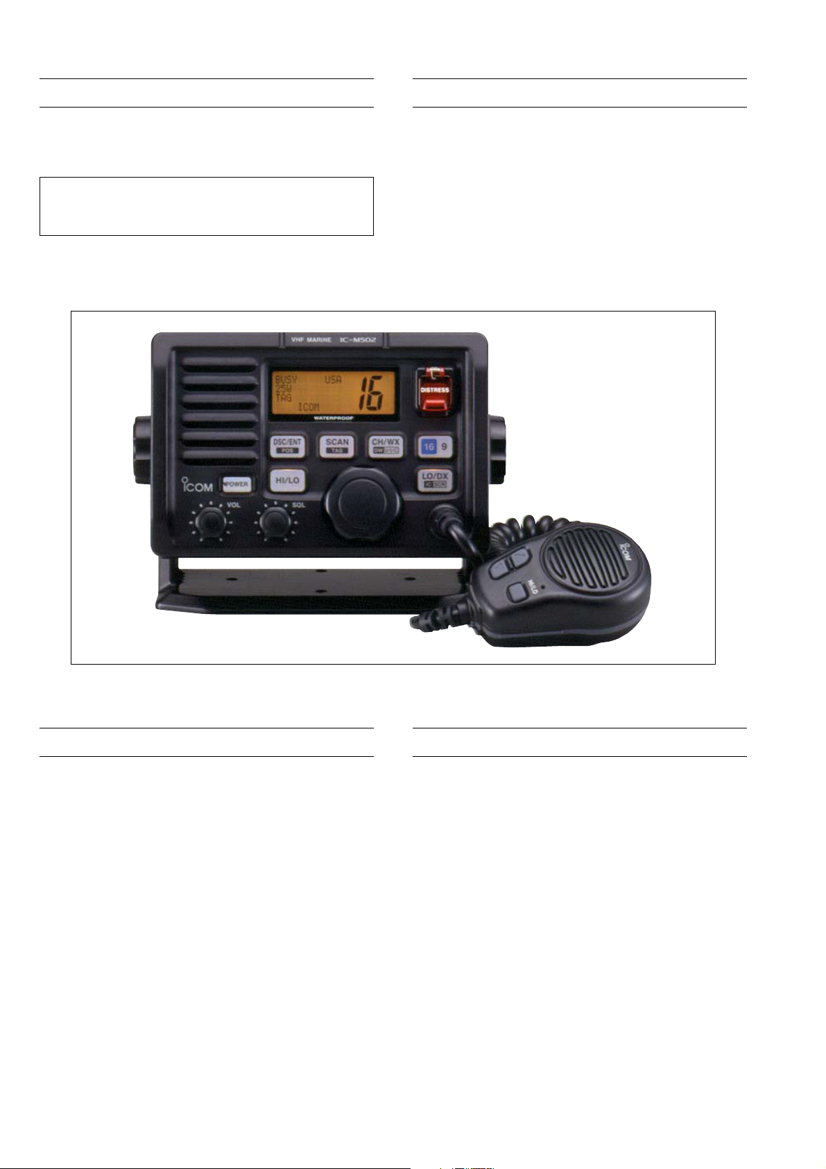
VHF MARINE TRANSCEIVER
iM502
SERVICE
MANUAL
INTRODUCTION
This service manual describes the latest service information
for the IC-M502 VHF MARINE TRANSCEIVER at the time of
publication
DANGER
NEVER connect the transceiver to an AC outlet or to a DC
power supply that uses more than 16 V. This will ruin the
transceiver.
DO NOT expose the transceiver to rain, snow or any liquids.
DO NOT reverse the polarities of the power supply when
connecting the transceiver.
DO NOT apply an RF signal of more than 20 dBm (100 mW)
to the antenna connector. This could damage the
transceIer’s front end.
ORDERING PARTS
Be sure to include the following four points when ordering
replacement parts:
1. 10-digit order numbers
2. Component part number and name
3. Equipment model name and unit name
4. Quantity required
<SAMPLE ORDER>
1110003200 S.IC TA31136FN IC-M502 MAIN UNIT 15 pieces
8810006050 Screw Icom screw E7 IC-M502 CHASSIS 10 pieces
Addresses are provided on the inside back cover for your
convenience.
REPAIR NOTES
1. Make sure a problem is internal before disassembling the
transceiver.
2. DO NOT open the transceiver until the transceiver is
disconnected from its power source.
3. DO NOT force any of the variable components. Turn
them slowly and smoothly.
4. DO NOT short any circuits or electronic parts. An insulated tuning tool MUST be used for all adjustments.
5. DO NOT keep power ON for a long time when the trans-
ceiver is defective.
6. DO NOT transmit power into a signal generator or a
sweep generator.
7. ALWAYS connect a 40 dB to 50 dB attenuator between
the transceiver and a deviation meter or spectrum analyzer when using such test equipment.
8. READ the instructions of test equipment thoroughly
before connecting equipment to the transceiver.
To upgrade quality, any electrical or mechanical parts and
internal circuits are subject to change without notice or
obligation.

TABLE OF CONTENTS
SECTION 1 SPECIFICATIONS
SECTION 2 INSIDE VIEWS
2 - 1 IC-M502 . . . . . . . . . . . . . . . . . . . . . . . . . . . . . . . . . . . . . . . . . . . . . . . . . . . . . . . . . . . . . . . . . . . . . . 2 - 1
2 - 2 HM-127 (OPTIONAL UNIT) . . . . . . . . . . . . . . . . . . . . . . . . . . . . . . . . . . . . . . . . . . . . . . . . . . . . . . . . 2 - 2
SECTION 3 DISASSEMBLY INSTRUCTION
SECTION 4 CIRCUIT DESCRIPTION
4 - 1 RECEIVER CIRCUITS . . . . . . . . . . . . . . . . . . . . . . . . . . . . . . . . . . . . . . . . . . . . . . . . . . . . . . . . . . . 4 - 1
4 - 2 TRANSMITTER CIRCUITS . . . . . . . . . . . . . . . . . . . . . . . . . . . . . . . . . . . . . . . . . . . . . . . . . . . . . . . 4 - 2
4 - 3 PLL CIRCUIT . . . . . . . . . . . . . . . . . . . . . . . . . . . . . . . . . . . . . . . . . . . . . . . . . . . . . . . . . . . . . . . . . 4 - 3
4 - 4 DSC CIRCUIT . . . . . . . . . . . . . . . . . . . . . . . . . . . . . . . . . . . . . . . . . . . . . . . . . . . . . . . . . . . . . . . . . 4 - 4
4 - 5 POWER SUPPLY CIRCUITS . . . . . . . . . . . . . . . . . . . . . . . . . . . . . . . . . . . . . . . . . . . . . . . . . . . . . . 4 - 4
4 - 6 LOGIC CIRCUITS . . . . . . . . . . . . . . . . . . . . . . . . . . . . . . . . . . . . . . . . . . . . . . . . . . . . . . . . . . . . . . 4 - 4
4 - 7 PORT ALLOCATIONS . . . . . . . . . . . . . . . . . . . . . . . . . . . . . . . . . . . . . . . . . . . . . . . . . . . . . . . . . . . 4 - 4
SECTION 5 ADJUSTMENT PROCEDURES
5 - 1 PREPARATION . . . . . . . . . . . . . . . . . . . . . . . . . . . . . . . . . . . . . . . . . . . . . . . . . . . . . . . . . . . . . . . . 5 - 1
5 - 2 PLL ADJUSTMENTS . . . . . . . . . . . . . . . . . . . . . . . . . . . . . . . . . . . . . . . . . . . . . . . . . . . . . . . . . . . . 5 - 2
5 - 3 TRANSMITTER ADJUSTMENTS . . . . . . . . . . . . . . . . . . . . . . . . . . . . . . . . . . . . . . . . . . . . . . . . . . . 5 - 3
5 - 4 RECEIVER ADJUSTMENTS . . . . . . . . . . . . . . . . . . . . . . . . . . . . . . . . . . . . . . . . . . . . . . . . . . . . . . . 5 - 4
SECTION 6 PARTS LIST
SECTION 7 MECHANICAL PARTS
7 - 1 IC-M502 . . . . . . . . . . . . . . . . . . . . . . . . . . . . . . . . . . . . . . . . . . . . . . . . . . . . . . . . . . . . . . . . . . . . . . 7 - 1
7 - 2 HM-126 . . . . . . . . . . . . . . . . . . . . . . . . . . . . . . . . . . . . . . . . . . . . . . . . . . . . . . . . . . . . . . . . . . . . . . 7 - 3
7 - 3 HM-127 (OPTIONAL UNIT) . . . . . . . . . . . . . . . . . . . . . . . . . . . . . . . . . . . . . . . . . . . . . . . . . . . . . . . . 7 - 3
SECTION 8 SEMI-CONDUCTOR INFORMATION
SECTION 9 BOARD LAYOUTS
9 - 1 VOL UNIT . . . . . . . . . . . . . . . . . . . . . . . . . . . . . . . . . . . . . . . . . . . . . . . . . . . . . . . . . . . . . . . . . . . . . 9 - 1
9 - 2 DIAL UNIT . . . . . . . . . . . . . . . . . . . . . . . . . . . . . . . . . . . . . . . . . . . . . . . . . . . . . . . . . . . . . . . . . . . . 9 - 1
9 - 3 SQL UNIT . . . . . . . . . . . . . . . . . . . . . . . . . . . . . . . . . . . . . . . . . . . . . . . . . . . . . . . . . . . . . . . . . . . . . 9 - 1
9 - 4 LOGIC UNIT . . . . . . . . . . . . . . . . . . . . . . . . . . . . . . . . . . . . . . . . . . . . . . . . . . . . . . . . . . . . . . . . . . . 9 - 2
9 - 5 MAIN UNIT . . . . . . . . . . . . . . . . . . . . . . . . . . . . . . . . . . . . . . . . . . . . . . . . . . . . . . . . . . . . . . . . . . . . 9 - 4
9 - 6 CTRL UNIT . . . . . . . . . . . . . . . . . . . . . . . . . . . . . . . . . . . . . . . . . . . . . . . . . . . . . . . . . . . . . . . . . . . 9 - 6
9 - 7 PWR-CORD UNIT . . . . . . . . . . . . . . . . . . . . . . . . . . . . . . . . . . . . . . . . . . . . . . . . . . . . . . . . . . . . . . 9 - 6
9 - 8 HM-126 . . . . . . . . . . . . . . . . . . . . . . . . . . . . . . . . . . . . . . . . . . . . . . . . . . . . . . . . . . . . . . . . . . . . . . 9 - 6
9 - 9 HM-127 (OPTIONAL UNIT) . . . . . . . . . . . . . . . . . . . . . . . . . . . . . . . . . . . . . . . . . . . . . . . . . . . . . . . . 9 - 6
SECTION 10 BLOCK DIAGRAM
SECTION 11 VOLTAGE DIAGRAM
11 - 1 LOGIC UNIT . . . . . . . . . . . . . . . . . . . . . . . . . . . . . . . . . . . . . . . . . . . . . . . . . . . . . . . . . . . . . . . . . . 11 - 1
11 - 2 MAIN UNIT . . . . . . . . . . . . . . . . . . . . . . . . . . . . . . . . . . . . . . . . . . . . . . . . . . . . . . . . . . . . . . . . . . . 11 - 2
11 - 3 HM-127 (OPTIONAL UNIT) . . . . . . . . . . . . . . . . . . . . . . . . . . . . . . . . . . . . . . . . . . . . . . . . . . . . . . . 11 - 4
11 - 4 HM-126 . . . . . . . . . . . . . . . . . . . . . . . . . . . . . . . . . . . . . . . . . . . . . . . . . . . . . . . . . . . . . . . . . . . . . . 11 - 5

1 - 1
SECTION 1 SPECIFICATIONS
‘‘
GENERAL
• Frequency coverage : 156.025–157.425 MHz (Tx)
156.050–163.275 MHz (Rx)
• Mode : 16K0G3E (FM)
16K0G2E (DSC)
• Usable channels : All international and USA channels
• Power supply requirement : 13.8 V DC (negative ground)
• Usable temperature range : –20˚C to +60˚C (–4 ˚F to +140˚F)
• Frequency stability : ±10 ppm (–20˚C to +60˚C; –4 ˚F to +140˚F)
• Current drain (at 13.8 V DC) : Transmit at 25 W 6.5 A
Receive max. audio 1.2 A
• Antenna connector : SO-239 (50 Ω)
• Dimensions (projections not included) : 165(W)×110(H)×109.4(D) mm
6
1
⁄2(W) ✕ 411⁄32(H) ✕ 45⁄16(D) in
• Weight : 1130 g (2 lb 8 oz)
‘‘
TRANSMITTER
• Output power (at 13.8 V DC) : High 25 W
Low 1 W
• Modulation : Variable reactance frequency modulation
• Maximum frequency deviation : ±5.0 kHz
• Spurious emissions : 70 dBc
• Adjacent channel power : 70 dB
• Residual modulation : 40 dB
• Audio harmonic distortion : Less than 10% at 60% deviation
• Audio frequency response : +1 dB to –3 dB of 6 dB octave from 300 Hz to 2500 Hz
• Microphone impedance : 600 Ω
‘‘
RECEIVER
• Receive system : Double conversion superheterodyne system
• Intermediate frequencies : 1st 21.7 MHz
2nd 450 kHz
• Sensitivity : 0.32 µV (–117 dBm) at 12 dB SINAD
• Squelch sensitivity : 0.32 µV at threshhold
• Adjacent channel selectivity : 75 dB
• Spurious response : 75 dB
• Intermodulation rejection ratio : 75 dB
• Hum and noise : 40 dB
• Audio output power (at 13.8 V DC) : 3.5 W typical at 10% distortion with an 4 Ω load
• Audio frequency responce : +1 dB to –3 dB of –6 dB octave from 300 Hz to 3000 Hz
Specifications are measured in accordance with TIA/EIA-603
All stated specifications are subject to change without notice or obligation.

1 - 2
*1Low power only, *2Receive only
NOTE: Simplex channels 3, 21, 23, 61, 64, 81, 82 and 83 CANNOT be lawfully used by the general public in USA waters.
CAN
21A
22A
23
24
25
26
27
28
60
61A
62A
64
64A
65A
66A*
1
67
68
69
70*
2
71
72
CAN
73
74
77*
1
78A
79A
80A
81A
82A
83
83A
84
85
86
87
88
CAN
01
02
03
04A
05A
06
07A
08
09
10
11
12
13*
1
14
15*
1
16
17*
1
18A
19A
20*
1
21
‘‘
VHF MARINE CHANNEL LIST
USA
01A
03A
05A
06
07A
08
09
10
11
12
13*
1
14
15*
1
16
17*
1
18A
19A
20
20A
INT
01
02
03
04
05
06
07
08
09
10
11
12
13
14
15*
1
16
17
18
19
20
21
Transmit
156.050
156.050
156.100
156.150
156.150
156.200
156.200
156.250
156.250
156.300
156.350
156.350
156.400
156.450
156.500
156.550
156.600
156.650
156.700
156.750
156.800
156.850
156.900
156.900
156.950
156.950
157.000
157.000
157.050
Receive
160.650
156.050
160.700
160.750
156.150
160.800
156.200
160.850
156.250
156.300
160.950
156.350
156.400
156.450
156.500
156.550
156.600
156.650
156.700
156.750
156.800
156.850
161.500
156.900
161.550
156.950
161.600
157.000
161.650
USA
21A
22A
23A
24
25
26
27
28
61A
63A
64A
65A
66A
67*
1
68
69
70*
2
71
72
INT
22
23
24
25
26
27
28
60
61
62
63
64
65
65A
66
66A
67
68
69
70*
2
71
72
Transmit
157.050
157.100
157.100
157.150
157.150
157.200
157.250
157.300
157.350
157.400
156.025
156.075
156.075
156.125
156.125
156.175
156.175
156.225
156.225
156.275
156.275
156.325
156.325
156.375
156.425
156.475
156.525
156.575
156.625
Receive
157.050
161.700
157.100
161.750
157.150
161.800
161.850
161.900
161.950
162.000
160.625
160.675
156.075
160.725
156.125
160.775
156.175
160.825
156.225
160.875
156.275
160.925
156.325
156.375
156.425
156.475
156.525
156.575
156.625
USA
73
74
77*
1
78A
79A
80A
81A
82A
83A
84
84A
85
85A
86
86A
87
87A
88
88A
INT
73
74
77
78
79
80
81
82
83
84
85
86
87
88
Transmit
156.675
156.725
156.875
156.925
156.925
156.975
156.975
157.025
157.025
157.075
157.075
157.125
157.125
157.175
157.175
157.225
157.225
157.275
157.275
157.325
157.325
157.375
157.375
157.425
157.425
Receive
156.675
156.725
156.875
161.525
156.925
161.575
156.975
161.625
157.025
161.675
157.075
161.725
157.125
161.775
157.175
161.825
157.225
161.875
157.275
161.925
157.325
161.975
157.375
162.025
157.425
Channel No. Frequency (MHz) Channel No.
Frequency (MHz) Channel No. Frequency (MHz)
WX01
WX02
WX03
WX04
WX05
Transmit
Receive only
Receive only
Receive only
Receive only
Receive only
Receive
162.550
162.400
162.475
162.425
162.450
WX06
WX07
WX08
WX09
WX10
Transmit
Receive only
Receive only
Receive only
Receive only
Receive only
Receive
162.500
162.525
161.650
161.775
163.275
Frequency (MHz) Frequency (MHz)
Weather
channel
Weather
channel
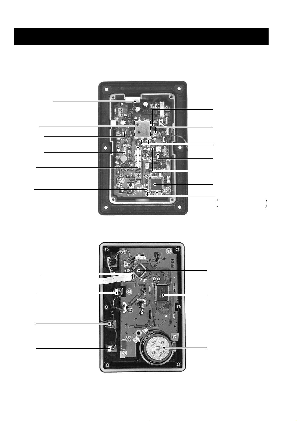
SECTION 2 INSIDE VIEWS
2 - 1
2-1 IC-M502
• LOGIC UNIT
• MAIN UNIT
AF power amplifier
(IC14: LA4425A)
PLL IC
(IC2: µPD3140GS)
VCO circuit
Drive amplifier
(Q12: 2SC2954)
Power module*
(IC3: SC-1302)
1st mixer*
(Q3: 3SK166)
Reset IC
(IC15: S-80928ANMP)
System clock
(X1: CSTCC4.91MG 4.91 MHz)
Reference oscillator
(X2: CR-659 21.25 MHz)
1st IF filter
(FI1, FI2: FL-310)
2nd IF filter
(FI3: ALFY450E)
FM IF IC
(IC1: TA31136FN)
Main MPU
(IC16: MB90F583BPFV-G)
System clock
X3: DMX-26S 36.768 kHz,
X4: CR-610 7.9872 MHz
* Located under side of the point
SUB MPU
(IC1: µPD789405AGK-A30-9EU)
DIAL UNIT
SQL UNIT
VOL UNIT
LCD driver
(IC2: HD66712SA03FS)
Speaker
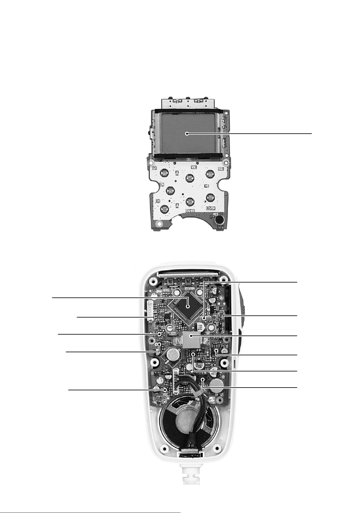
2 - 2
2-2 HM-127 (OPTIONAL UNIT)
• BOTTOM VIEW
• TOP VIEW
LCD
(DS1: A0119)
CPU
(IC1: µPD789405AGK-A30-9EU)
Data buffer circuit
Reset IC
(IC7: S-80928ANMP)
5V regulator
(IC5: TA78L05F)
MIC amplifier
(IC4: NJM2125F)
System clock
(X1: CSTCC4.91MG)
Dimmer circuit
8V regulator
(IC6: TA7808F)
Volume IC
(IC3: M62429FP)
AF/MIC switch
(IC9: TC4W53FU)
AF amplifier
(IC2: TA7368F)
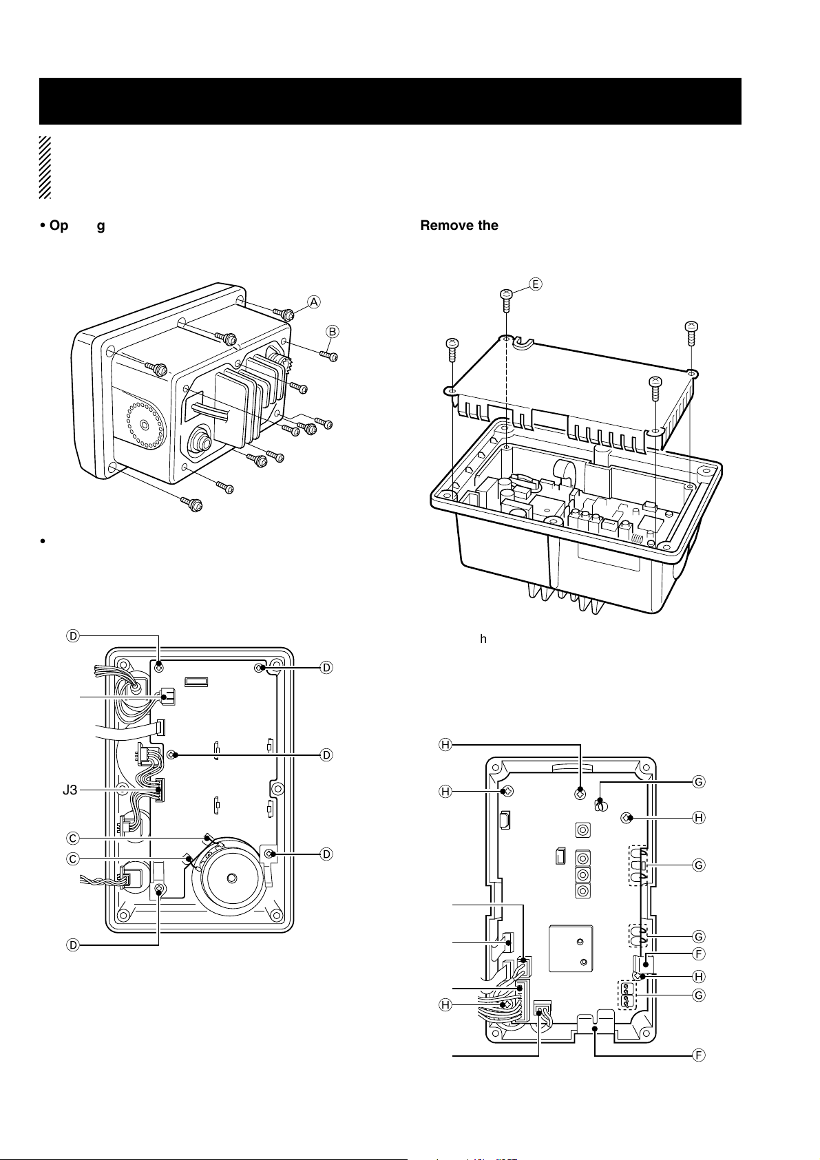
SECTION 3 DISASSEMBLY INSTRUCTION
3 - 1
CAUTION: DISCONNECT the DC power cable from
the transceiver before performing any work on the transceiver. Otherwise, there is danger of electric shock and/or
equipment damage.
• Removing the LOGIC unit
q Unsolder 2 point C.
w Disconnect microphone connector from J1 and SQL/DIAL
connector from J3.
e Unscrew 5 screws D, and remove the LOGIC unit.
• Opening the transceiver case
q Unscrew 6 screws A, and remove the front unit.
w Unscrew 6 screws B, and remove the rear panel.
w Remove the 2 clips F.
e Disconnect microphone connector from J7 and CTRL
connector from J3 and EX-SP connector from J8 and
EX-GPS connector from J2.
r Unsolder 10 point G.
t Unscrew 5 screws H, and remove the MAIN unit.
• Remove the MAIN unit
q Unscrew 4 screws E from the shielding plate, then lift up
the shielding plate.
A
B
E
D
J1
J3
C
C
D
D
D
D
H
H
G
H
G
J2
J3
G
F
H
J7
H
G
J8
F
SECTION 4 CIRCUIT DESCRIPTION
4 - 1
4-1 RECEIVER CIRCUITS
4-1-1 ANTENNA SWITCHING CIRCUIT
The antenna switching circuit functions as a low-pass filter
while receiving and as resonator circuit while transmitting.
The circuit does not allow transmit signals to enter receiver
circuits.
Received signals enter the MAIN unit from the antenna connector and pass through the low-pass filter (L23–L25, C134,
C136–C139). The signals are then applied to the RF circuit
via the antenna switching circuit (D17, L26, L27,
C141–C143).
4-1-2 RF CIRCUIT
The RF circuit amplifies signals within the range of frequency coverage and filters out-of-band signals.
The signals from the antenna switching circuit pass through
a tunable bandpass filter (D1, L1, C2–C4) where the object
signals are led to the RF amplifier circuit (Q2).
The amplified signals at Q2 are applied to the 3-stage tunable bandpass filter (D2–D4, D34–D36, L2–L4, C13, C14,
L33, C16–C18, C20–C24) to suppress unwanted signals
and improve the selectivity. The signals are then applied to
the 1st mixer circuit.
D1–D4, D34–D36 employ varactor diodes, that are controlled by the PLL lock voltage, to track the band pass filters.
4-1-3 1ST MIXER AND 1ST IF CIRCUITS
The 1st mixer circuit converts the received signal into a fixed
frequency of the 1st IF signal with a 1st LO (VCO output) frequency. By changing the 1st LO frequency, only the desired
frequency will pass through a pair of crystal filters at the next
stage of the mixer.
The signals from the RF circuit are mixed with the VCO signals at the 1st mixer circuit (Q3) to produce a 21.7 MHz 1st
IF signal.
The 1st IF signal is applied to a pair of crystal filters (FI1,
FI2) to suppress out-of-band signals and is then amplified at
the IF amplifier (Q4). The amplified signal is applied to the
2nd mixer circuit (IC1).
4-1-4 2ND IF AND DEMODULATOR CIRCUITS
The 2nd mixer circuit converts the 1st IF signal into a 2nd IF
signal. A double superheterodyne system (which converts
receive signals twice) improves the image rejection ratio and
obtains stable receiver gain.
The FM IF IC (IC1) contains the 2nd local oscillator, 2nd
mixer, limiter amplifier, quadrature detector, and noise
detector circuits, etc.
The 1st IF signal from Q4 is applied to the 2nd mixer section
of IC1 (pin 16), and is mixed with a 21.25 MHz 2nd LO signal generated at the PLL circuit using the reference frequency (21.25 MHz) to produce a 450 kHz 2nd IF signal.
The 2nd IF signal from IC1 (pin 3) is passed through the
ceramic filter (FI3), where unwanted signals are suppressed, and is then applied to the 2nd IF (limiter) amplifier
in IC1 (pin 5). The signal is applied to the FM detector section in IC1 for demodulation into AF signals.
The FM detector circuit employs a quadrature detection
method (linear phase detection), which uses a ceramic discriminator (X1) for phase delay to obtain a non-adjusting circuit. The detected signal from IC1 (pin 9) is applied to the AF
circuit.
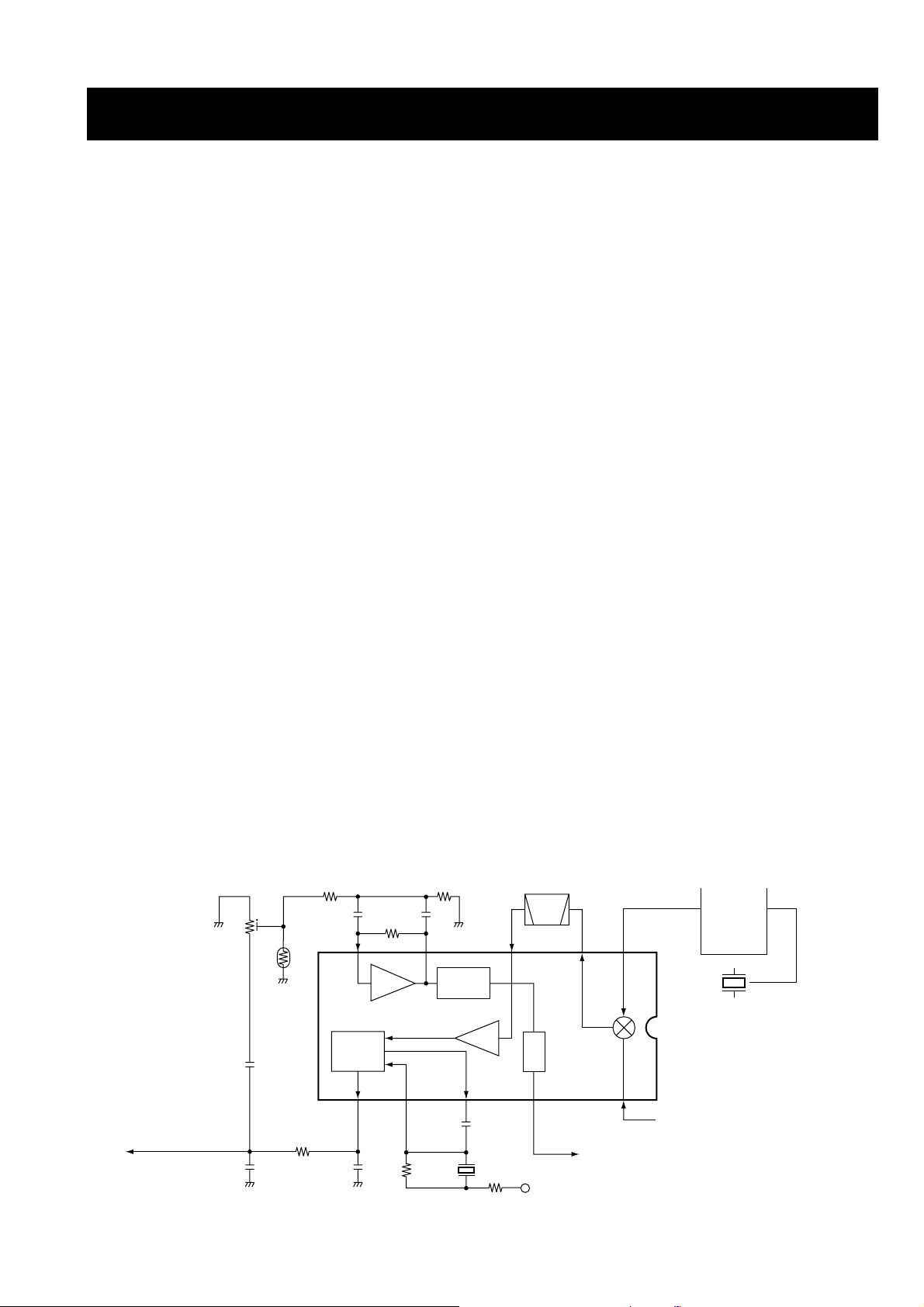
• 2nd IF and demodulator circuits
Mixer
16
Limiter
amp.
2nd IF filter
450 kHz
PLL IC
IC2
X2
21.25 MHz
X1
(21.25 MHz)
RSSI
IC1 TA31136FN
14
1st IF (21.7 MHz) from Q4
"SQLI" signal to the DC amplifier (IC20, pin 1)
11109
87 5 3
AF signal "DEMOD"
R8V
Squelch level
adjustment pot
2
17
16
Active
filter
FI3
Noise
detector
FM
detector
4 - 2
4-1-5 AF AMPLIFIER CIRCUIT
The AF amplifier circuit amplifies the detected signals to
drive a speaker. The AF circuit includes an AF mute circuit
for the squelch.
AF signals from IC1 (pin 9) are passed through the analog
switch (IC12, pins 10, 11), and are applied to the de-emphasis circuit (R118, C182). The de-emphasis circuit is an integrated circuit with frequency characteristic of –6 dB/octave.
The integrated signals are applied to the active filters (Q24,
Q25). Q24 functions as a high-pass filter to suppress
unwanted lower noise signals and Q25 functions as a lowpass filter to suppress higher noise signals.
The filtered signals are passed through the [VOLUME] control, and are then applied to the AF power amplifier (IC14,
pin 1). The output signal from IC14 (pin 4) drives the internal (external) speaker.
4-1-6 SQUELCH CIRCUIT
A squelch circuit cuts out AF signals when no RF signals are
received. By detecting noise components in the AF signals,
the squelch circuit switches the AF mute switch.
A portion of the AF signals from the FM IF IC (IC1, pin 9)
pass through the squelch adjustment pot (R33), and are
then applied to the active filter section (IC1, pin 8). The
active filter section amplifies and filters noise components.
The filtered signals are applied to the noise detector section
and output from pin 14 as the “SQLI” signal. The “SQLI” signal is amplified at the DC amplifier (IC20) and applied to the
CPU (IC16, pin 39) as the “SQL” signal. The CPU analyzes
the noise condition and outputs the “RMUTM”, “RMUTS”
signals to toggle the AF mute switches (Q26, Q27).
4-2 TRANSMITTER CIRCUITS
4-2-1 MICROPHONE AMPLIFIER CIRCUIT
The microphone amplifier circuit amplifies audio signals with
+6 dB/octave pre-emphasis from the microphone to a level
needed at the modulation circuit.
The AF signals from the microphone are amplified at the
microphone amplifier (IC11a) via the analog switch (IC10,
pins 11, 10). A capacitor (C214) and resistor (R147) are connected to the amplifier to obtain the pre-emphasis characteristics.
The amplified signals are applied to the IDC amplifier
(IC13a, pin 2) via the analog switch (IC12, pins 9, 8 and pins
4, 3) and are passed through the splatter filter (IC13b) to
suppress unwanted 3 kHz or higher signals. The filtered signals are then applied to the modulation circuit.
4-2-2 MODULATION CIRCUIT
The modulation circuit modulates the VCO oscillating signal
(RF signal) using the microphone audio signals.
Audio signals from the splatter filter (IC13b) pass through
the frequency deviation adjustment pot (R172) and are then
applied to the modulation circuit (D8) to change the reactance of D8, and modulate the oscillated signal at the TXVCO (Q7).
4-2-3 DRIVE AMPLIFIER CIRCUIT
The drive amplifier circuit amplifies the VCO oscillating signal to a level needed at the power amplifier.
The VCO output is buffer-amplified by Q9 and Q10, and is
then applied to the Tx/Rx switch (D12). The transmit signal
from the Tx/Rx switch is amplified to the pre-drive (Q11) and
drive (Q12) amplifiers to obtain an approximate 200 mW signal level. The amplified signal is then applied to the RF
power amplifier (IC3).
4-2-4 POWER AMPLIFIER CIRCUIT
The power amplifier circuit amplifies the driver signal to an
output power level.
IC3 is a power module which has amplification output capabilities of about 35 W with 300 mW input. The output from
IC3 (pin 4) is passed through the antenna switching circuit
(D16) and is then applied to the antenna connector via the
low-pass filter.
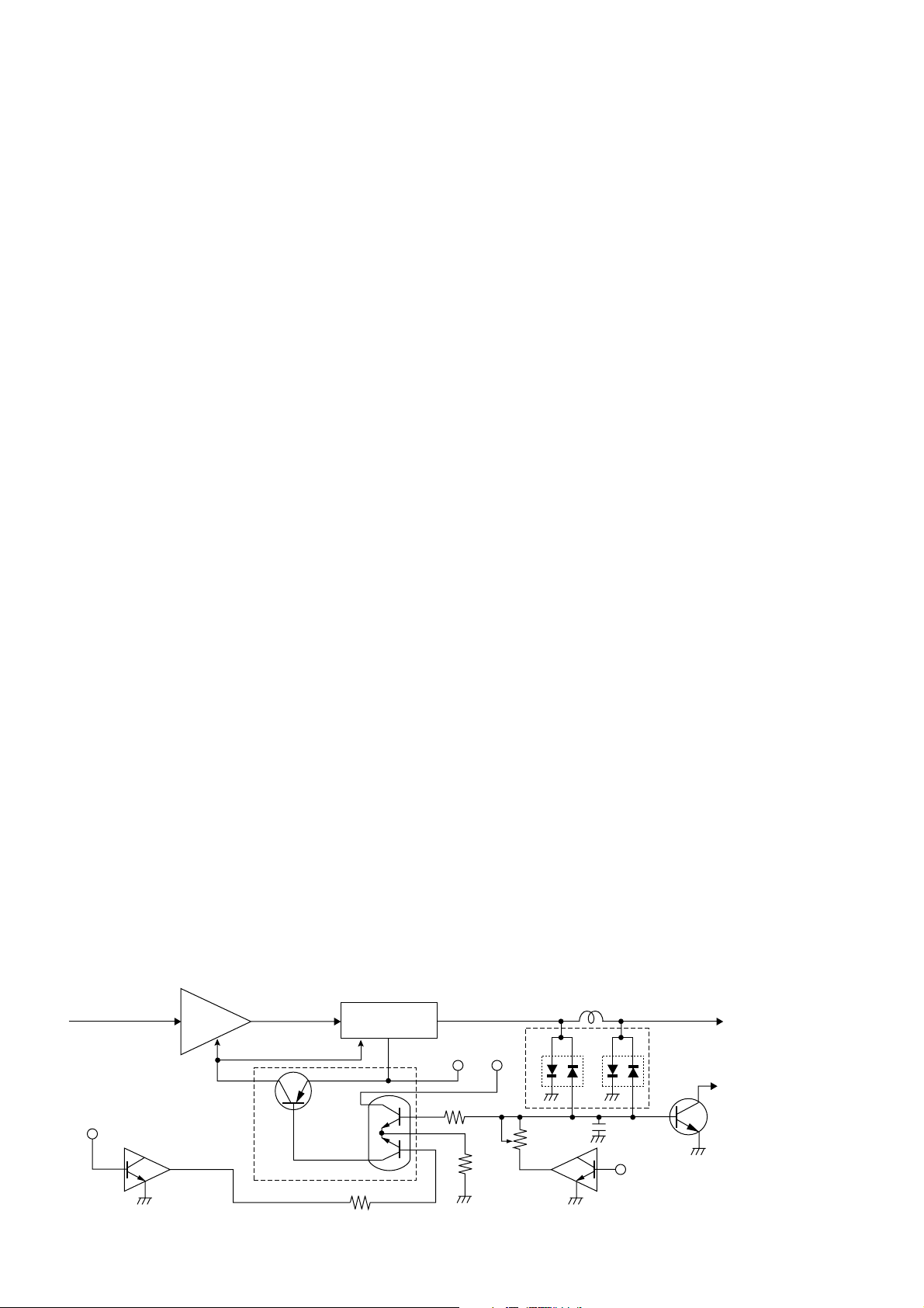
4-2-5 APC CIRCUIT
The APC circuit stabilizes transmit output power.
The RF output signal from the power amplifier (IC3) is
detected at the power detector circuit (D14, D15, L21) and
is then applied to one of the differential amplifier inputs
(Q16, pin 5) via the High/Low control circuit (R84, Q17). The
applied voltage controls the differential amplifier output
(Q16, pin 2) and the bias voltage control (Q14). Thus the
APC circuit maintains a constant output power.
• APC circuit
T8
D14
D15
L21
/TMUT
VCC
HI/LO
"TXDET" signal
to the CPU
Q14
Q16
Q15
Q17
R84
Q12
Drive
amp.
RF signal
from PLL
to antenna
RF detector
circuit
APC control circuit
Power module
IC3
Q18
4 - 3
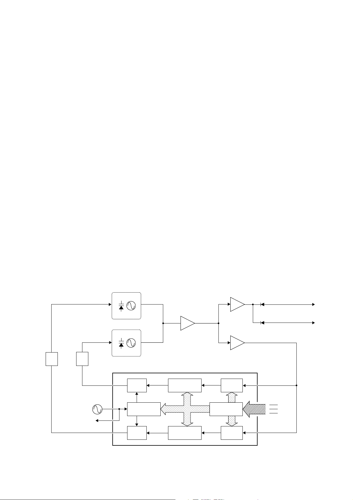
4-3 PLL CIRCUITS
4-3-1 GENERAL
The PLL circuit provides stable oscillation of the transmit frequency and receive 1st LO frequency. The PLL circuit compares the phase of the divided VCO frequency to the reference frequency. The PLL output frequency is controlled by a
crystal oscillator and the divided ratio of the programmable
divider.
IC2 is a dual PLL IC which controls both VCO circuits for Tx
and Rx, and contains a prescaler, programmable counter,
programmable divider phase detector, charge pomp and etc.
The PLL circuit, using a one chip PLL IC (IC2), directly generates the transmit frequency and receive 1st IF frequency
with VCOs. The PLL sets the divided ratio based on serial
data from the CPU and compares the phases of VCO signals with the reference oscillator frequency. The PLL IC
detects the out-of-step phase and output from pins 8 and 13
for Tx and Rx, respectively. The reference frequency (21.25
MHz) is oscillated at X2.
4-3-2 TX LOOP
The generated signal at the TX-VCO (Q7, D6–D8) enters
the PLL IC (IC2, pin 2) and is divided at the programmable
divider section and is then applied to the phase detector
section.
The phase detector compares the input signal with a reference frequency, and then outputs the out-of-phase signal
(pulse-type signal) from pin 8.
The pulse-type signal is converted into DC voltage (lock
voltage) at the loop filter (R252–R254, C292–C294), and is
then applied to varactor diodes (D6, D7) of the TX-VCO to
stabilize the oscillated frequency.
4-3-3 RX LOOP
The generated signal at the RX-VCO (Q8, D9, D10) enters
the PLL IC (IC2, pin 19) and is divided at the programmable
divider section and is then applied to the phase detector
section.
The phase detector compares the input signal with a reference frequency, and then outputs the out-of-phase signal
(pulse-type signal) from pin 13.
The pulse-type signal is converted into DC voltage (lock
voltage) at the loop filter (R255–R257, C295, C296), and is
then applied to varactor diodes (D9, D10) of the RX-VCO to
stabilize the oscillated frequency. The lock voltage is also
used for the receiver circuit for the bandpass filter center frequency. The lock voltage from the loop filter is amplified at
the buffer-amplifier (Q6) and then applied to the RF circuit.
4-3-4 VCO CIRCUIT
The VCO outputs from TX-VCO (Q7) and RX-VCO (Q8) are
amplified at the buffer amplifiers (Q9 and Q10), and are then
sent to the Tx/Rx switch (D11, D12). The receive LO signal
is applied to the 1st mixer circuit (Q3) through a low-pass filter, and the transmit signal is applied to the pre-drive amplifier (Q11). A portion of the VCO output is reapplied to the
PLL IC (IC2, pin 2 or pin 13) via the buffer amplifier (Q5).
• PLL circuit
Loop
filter
Loop
filter
X2
21.25 MHz
Shift register/
data latch
IC2 (PLL IC)
Prescaler
Phase
detector
Programmable
counter
Prescaler
Phase
detector
Programmable
counter
Programmable
divider
3
4
5
2
8
19
13
PSTB
CK
DATA
21.25 MHz signal
to the FM IF IC
Buffer
Buffer
Buffer
Q10
Q5
Q9
to transmitter circuit
to 1st mixer circuit
D11
D12
17
16
Q7, D6–D8
TX-VCO
Q8, D9, D10
RX-VCO
4 - 4
4-4 DSC CIRCUITS (DSC UNIT)
4-4-1 DSC ENCODE CIRCUIT
The DSC signal created at CPU (IC16), is passed through
the buffer amplifier (Q33) and applied to the analog switch
(IC12, pin 1). The analog switch (IC12) is a modulation
switch that switches between microphone audio signal and
DSC signal.
4-4-2 DSC DECODE CIRCUT
The AF signals from FM IF IC (IC1, pin 9) are filtered at the
bandpass filter (IC4) with +18 dB/octave characteristics.
IC4b functions as a low-pass filter to suppress unwanted
higher noise signals and IC4a functions as a high-pass filter
to suppress lower noise signals. The filtered signals are converted analog signals into digital signals at DSC decoder IC
(IC5), and are then applied to the CPU (IC16) after shaping
waveform at IC6.
4-5 POWER SUPPLY CIRCUITS
4-5-1 VOLTAGE LINE (MAIN UNIT)
4-6 LOGIC CIRCUITS
4-6-1 MAIN UNIT
• MPU
IC16 is a 16 bit multifunction micro-computer and contains
FLASH memory, serial I/O, timer, A/D converter, D/A converter, programmable I/O, ROM and RAM.
• SYSTEM CLOCK CIRCUIT
X3, X4 are crystal oscillators and oscillate 7.9872 MHz and
32.768 kHz system clocks for the MPU (IC16) respectively.
• RESET CIRCUIT
IC15 is a reset IC. When turn power ON, IC15 outputs a
reset signal (“LOW” pulse) to MPU (IC16, pin 75).
• LOW BATTERY DETECTOR
VCC voltage is divided by R204, R205 and is applied to the
low battery detector section in the MPU (IC16, pin 42).
4-6-2 LOGIC UNIT
• CPU
IC1 is an 8 bit single chip micro-computer and contains LCD
driver, serial I/O, timer, A/D converter, programmable I/O,
ROM and RAM.
• SYSTEM CLOCK CIRCUIT
X1 is a ceramic oscillator and oscillates a 4.91 MHz system
clock for the CPU (IC1).
• LCD DRIVER
IC2 is a LCD driver for a dot matrix LCD.
• DIMMER CIRCUIT
CPU (IC1) and Q2, Q3, Q8 are dimmer circuit and control
the LCD backlight (LED).
• CONTRAST CIRCUIT
CPU (IC1) and Q1, Q4 are contrast circuit and control the 8
step display contrast.
4-7 PORT ALLOCATIONS
4-7-1 SUB CPU (LOGIC unit; IC1)
LINE
HV
HVS
VCC
8V
+5V
T8
R8
DESCRIPTION
The voltage from the connected DC power supply.
Same voltage as the HV line which is passed
through the [PWR] switch (LOGIC unit; S1).
Same voltage as the HVS line which is passed
through the power controller (RL1).
Common 8 V converted from the VCC line at the
8V regulator circuit (IC8).
Common 5 V converted from the 8V line at the
+5V regulator circuit (IC9).
Transmit 8 V controlled by the T8 control circuit
(Q20, Q21) using the SEND signal from CPU.
Receive 8 V controlled by the R8 control circuit
(Q22, Q23) using the RCV signal from CPU. The
controlled voltage is applied to the receiver circuits.
27,
28, 29, 30
31–38
42
43
44
46
47
51, 52
54
55
58–60
61
62
63
64
75–77
78–80
LRESET,
E, RW, RS
DB7–
DB0
SCAN
CHWX
CH16
SQLV
KEYM
DIALA,
DIALB
SRXD
STXD
CONTSEG3–
CONTSEG1
DTRS
IC
DSC
HL
DIM3–
DIM1
CONDOT3–
CONDOT1
Output ports for the LCD driver (IC2)
control signals.
I/O port for the LCD driver (IC2) control
signals.
Input port for the [SCAN] key.
Input port for the [CH/WX] key.
Input port for the [16/9] key.
Input port for the squelch volume level.
Input port from the microphone (HM-
126) for remote control signal
Input ports for the [CHANNEL].
Outputs communication data for main
CPU (MAIN unit; IC16).
Input port for the communication data
from main CPU (MIAN unit; IC16).
Output port for the LCD contrast.
Input port for the [DISTRESS] key.
Input port for the [LO/DX] key.
Input port for the [DSC/ENT] key.
Input port for the [HI/LO] key.
Output LCD backlight control signal for
the dimmer circuit (Q2, Q3, Q8).
Output port for the LCD contrast.
Pin Port
Description
number name

4 - 5
4-7-2 MAIN CPU (MAIN unit; IC16)
Output port for the cloning data to the
buffer (MAIN unit; Q37).
Outputs clock signal for EEPROM
(IC17).
Outputs serial data signal for EEPROM (IC17).
Outputs select signal to the analog
switch (IC12) for the microphone audio
signal or DSC signal.
D/A output port for the ATIS/DSC
encode signal to the buffer amplifier
(Q33).
Input port from the FM IF IC (IC1) for
the squelch operation.
Input port for the connected power
supply voltage detection (low battery
indicator).
Input port for the “TX” indicator from
the power detector circuit (D14, D15).
Input port for the ATIS/DSC decode
signal.
Input port for the PLL unlock signal.
Low : While PLL is locked.
Input port for the PTT switch.
Input port for the microphone hanger
detection signal.
Low : Microphone on hook
Input port for the optional unit connection detection.
Outputs the R8 regulator (Q22, Q23)
control signal.
Low : While receiving
Outputs the AF mute switch (Q26)
control signal for main body.
Low : While squelched
Outputs the AF mute switch (Q27)
control signal for the optional remote
microphone (HM-127).
Low : While squelched
Outputs beep audio for main body.
Outputs beep audio for the optional
remote microphone (HM-127).
Input port for the reset signal.
Outputs the reset signal for sub CPU
(LOGIC unit; IC1).
CLTX
ECK
EDA
MICDSC
DSC
SQL
LBAT
TXDET
DSDEC
UNLK
PTT
HANG
OPTIN
RCV
RMUTM
RMUTS
BEEPM
BPLVM
RESET
SRESET
20
23
24
27
30
39
42
44
45
46
60
61
62
66
67
68
69
71
75
100
1
2
3
4
5
6
7
8
10
11
12
13
14
15
16
17
19
STRU
SCON
OPSTB
PSTB
CK
DATA
PTTM
PTTS
MMUTE
SMUTE
SP
HI/LO
SEND
TMUTE
SRXD
STXD
CLRX
Outputs control signal to the analog
switch (IC12) for passing through the
optional VOICE SCRAMBLER unit
(UT98 or UT-112).
Outputs ON/OFF control signal for the
optional VOICE SCRAMBLER unit
(UT-98 or UT-112).
Outputs strobe signals for the optional
VOICE SCRAMBLER unit UT-98 or
UT-112.
Outputs strobe signals to PLL IC (IC2,
pin 2).
Outputs clock signal to PLL IC (IC2,
pin 3).
Outputs clock signal to PLL IC (IC2,
pin 4).
Outputs main microphone (HM-126)
select signal to the analog switch
(IC10) while intercom operation.
Outputs optional remote microphone
(HM-127) select signal to the analog
switch (IC10) while intercom
operation.
Outputs select signal for the speaker
of main microphone (HM-126) to the
analog switch (IC10) while intercom
operation.
Outputs select signal for the speaker
of optional remote microphone (HM-
127) to the analog switch (IC10) while
intercom operation.
Outputs ON/OFF control signal for the
internal speaker to the AF mute circuit
(Q32, D23, RL2).
Low : While internal speaker is ON.
Output port for RF output power (High
or Low) select signal.
Low : While low power is selected.
Outputs the T8 regulator (Q20, Q21)
control signal.
Low : While transmitting
Outputs transmit mute signal.
High : While transmitting
Input port for the communication data
from sub CPU (LOGIC unit; IC1).
Outputs communication data for sub
CPU (LOGIC unit; IC1).
Input port for the cloning data from the
buffer (D24).
Pin Port
Description
number name
Pin Port
Description
number name
5 - 1
SECTION 5 ADJUSTMENT PROCEDURES
5-1 PREPARATION
■ REQUIRED TEST EQUIPMENT
EQUIPMENT
DC power supply
RF power meter
(terminated type)
Frequency counter
FM deviation meter
DC voltmeter
GRADE AND RANGE
Output voltage : 13.8 V DC
Current capacity : 10 A or more
Measuring range : 1–50 W
Frequency range : 100–300 MHz
Impedance : 50 Ω
SWR : Less than 1.2 : 1
Frequency range : 0.1–300 MHz
Frequency accuracy : ±1 ppm or better
Sensitivity : 100 mV or better
Frequency range : 30–300 MHz
Measuring range : 0 to ±10 kHz
Input impedance : 50 kΩ/V DC or better
EQUIPMENT
Audio generator
Standard signal
generator (SSG)
Oscilloscope
AC millivoltmeter
External speaker
Attenuator
GRADE AND RANGE
Frequency range : 300–3000 Hz
Measuring range : 1–500 mV
Frequency range : 0.1–300 MHz
Output level : 0.1 µV–32 mV
(–127 to –17 dBm)
Frequency range : DC–20 MHz
Measuring range : 0.01–20 V
Measuring range : 10 mV–10 V
Input impedance : 4 Ω
Capacity : 5 W or more
Power attenuation : 40 or 50 dB
Capacity : 50 W or more
‘‘
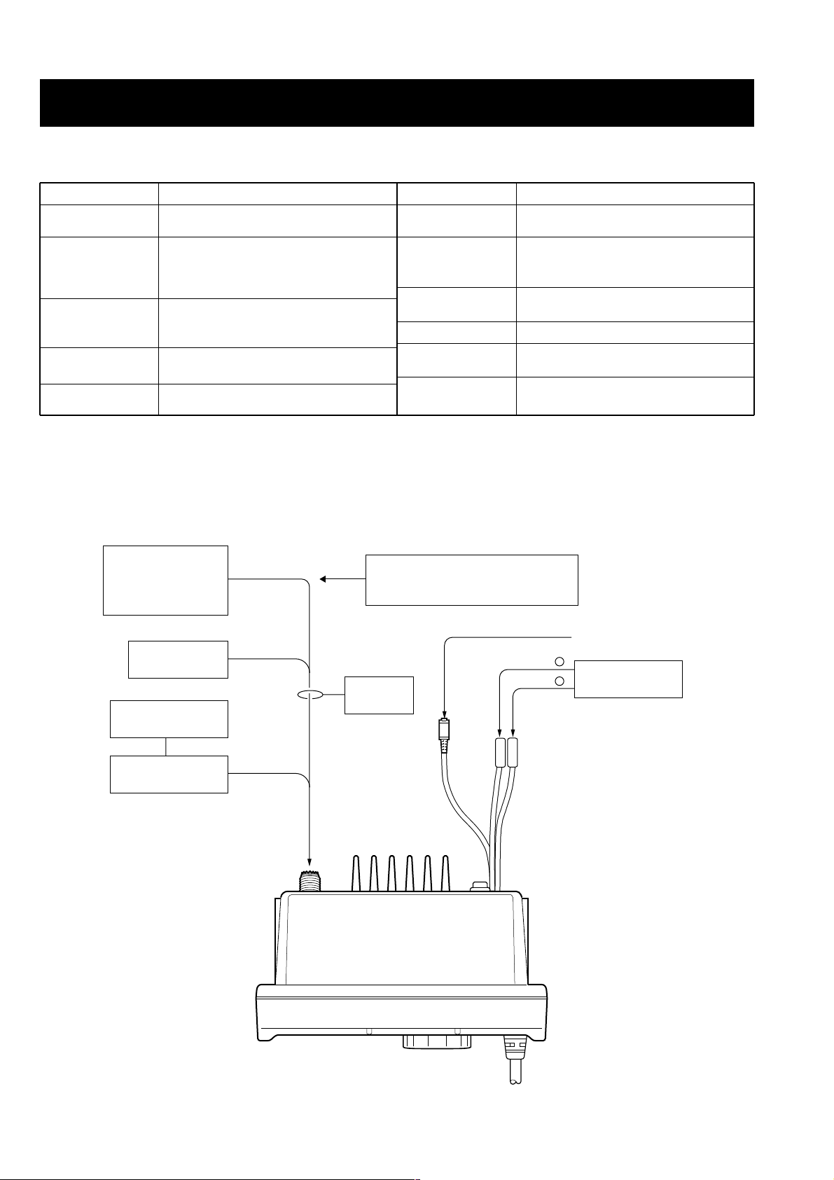
CONNECTIONS
to the antenna connector
Standard signal
generator
–17 to –125 dBm
(32 mV to 0.13 µV)
CAUTION:
DO NOT transmit while SSG is
connected to the antenna connector.
Frequency
counter
FM deviation
meter
Attenuator
40 dB or 50 dB
to DC cable
DC power supply
13.8 V /15 A
–
+
Black Red
RF power meter
50 Ω / 1–50 W
To external speaker
iM502

5 - 2
5-2 PLL ADJUSTMENTS
LOCK
VOLTAGE
REFERENCE
FREQUENCY
ADJUSTMENT
ADJUSTMENT ADJUSTMENT CONDITION
MEASUREMENT
VALUE
POINT
UNIT LOCATION UNIT ADJUST
1
2
3
4
1
• Operating channel : ch16
• Receiving
• Operating channel : ch116
• Receiving
• Operating channel : ch16
• Output power : Low
• Transmitting
• Operating channel : ch116
• Output power : Low
• Transmitting
• Operating channel : ch16
• Output power : Low
• Connect an RF power meter or a
50 Ω dummy load to the antenna
connector.
• Transmitting
MAIN
Rear
Panel
Connect a digital
multi-meter or oscilloscope to check
point CP1.
Connect a digital
multi-meter or oscilloscope to check
point CP2.
Loosely couple the
frequency counter
to the antenna connector.
3.5 V
4.5–6.0 V
2.5 V
2.5–3.5 V
156.8000 MHz
MAIN
MAIN
L13
Verify
L10
Verify
C70
Lock voltage
adjustment for TX
L10
Reference frequency
adjustment
C70
Lock voltage
check point for RX
CP1
Lock voltage
check point for TX
CP2
Lock voltage
adjustment for RX
L13

5-3 TRANSMITTER ADJUSTMENTS
5 - 3
OUTPUT
POWER
FREQUENCY
DEVIATION
ADJUSTMENT
ADJUSTMENT ADJUSTMENT CONDITION
MEASUREMENT
VALUE
POINT
UNIT LOCATION UNIT ADJUST
11• Operating channel : ch16
• Output power : High
• Transmitting
• Operating channel : ch16
• Output power : Low
• Connect an audio generator to J7
(pin 5) with an AC millivoltmeter
and set as:
Frequency : 1 kHz
Level : 70 mV
• Set an FM deviation meter as:
HPF : OFF
LPF : 20 kHz
De-emphasis : OFF
Detector : (P–P)/2
• Transmitting
Rear
Panel
Rear
Panel
Connect an RF
power meter to the
antenna connector.
Connect an FM
deviation meter to
the antenna connector through an
attenuator.
25 W
±4.3 kHz
MAIN
MAIN
R84
R172
Output power
adjustment
R84
Frequency deviation
adjustment
R172
–
+
[PTT]
J7
1
8
Audio generator
300 Hz to 3 kHz
AC millivoltmeter
2–200 mV

5 - 4
*This output level of a standard signal generator (SSG) is indicated as SSG’s open circuit.
5-4 RECEIVER ADJUSTMENTS
SENSITIVITY
SQUELCH
ADJUSTMENT
ADJUSTMENT ADJUSTMENT CONDITION
MEASUREMENT
VALUE
POINT
UNIT LOCATION UNIT ADJUST
11• Operating channel : ch16
• [SQUELCH] control:
Max. counterclockwise
• Set the internal speaker OFF in
the SET mode, and connect a
distortion meter with a 4 Ω load to
[EXT SP] receptacle.
• Connect an SSG to the antenna
connector and set as:
Frequency : 156.800 MHz
Level : 10 µV*
(–97 dBm)
Modulation : 1 kHz
Deviation : ±3.5 kHz
• Receiving
• Operating channel : ch16
• [SQUELCH] control:
Max. counterclockwise
• Connect an SSG to the antenna
connector and set as:
Frequency : 156.800 MHz
Level : 0.18 µV*
(–122 dBm)
Modulation : 1 kHz
Deviation : ±3.5 kHz
• Receiving
MAIN
MAIN
Connect a DC voltmeter to check point
CP3.
Connect a DC voltmeter to check point
CP5.
Maximum voltage
2 V
MAIN
MAIN
L1,
L2,
L3,
L4,
R33
Receive sensitivity
adjustment
L4
L3
L2
L1
Squelch check point
CP5
Squelch
adjustment
R33
Receive sensitivity
check point
CP3

6 - 1
SECTION 6 PARTS LIST
6-1 IC-M502
[LOGIC UNIT]
[LOGIC UNIT]
S.=Surface mount
IC1 1140009280 S.IC µPD78F9418AGK-9EU
IC2 1140008960 S.IC HD66712SA03FS
Q1 1560000810 S.FET 2SK1069-4-TL
Q2 1530002850 S.TRANSISTOR 2SC4116-BL (TE85R)
Q3 1520000460 S.TRANSISTOR 2SB1132 T100 R
Q4 1560000810 S.FET 2SK1069-4-TL
Q5 1590000720 S.TRANSISTOR DTA144EUA T106
Q6 1590000430 S.TRANSISTOR DTC144EUA T106
Q8 1530002850 S.TRANSISTOR 2SC4116-BL (TE85R)
D1 1790001010 S.ZENER MA8043-L (TX)
X1 6060000750 S.CERAMIC CSTCC4.91MG
R1 7030003640 S.RESISTOR ERJ3GEYJ 473 V (47 kΩ)
R2 7030003560 S.RESISTOR ERJ3GEYJ 103 V (10 kΩ)
R3 7030003640 S.RESISTOR ERJ3GEYJ 473 V (47 kΩ)
R4 7030003560 S.RESISTOR ERJ3GEYJ 103 V (10 kΩ)
R5 7030003640 S.RESISTOR ERJ3GEYJ 473 V (47 kΩ)
R6 7030003570 S.RESISTOR ERJ3GEYJ 123 V (12 kΩ)
R7 7030003460 S.RESISTOR ERJ3GEYJ 152 V (1.5 kΩ)
R8 7030003560 S.RESISTOR ERJ3GEYJ 103 V (10 kΩ)
R9 7510001150 S.THERMISTOR NTCCM1608 4BH 103KC
R10 7030003560 S.RESISTOR ERJ3GEYJ 103 V (10 kΩ)
R11 7030004120 S.RESISTOR ERJ3GEYJ 203 V (20 kΩ)
R12 7030003560 S.RESISTOR ERJ3GEYJ 103 V (10 kΩ)
R13 7030003590 S.RESISTOR ERJ3GEYJ 183 V (18 kΩ)
R14 7030003560 S.RESISTOR ERJ3GEYJ 103 V (10 kΩ)
R15 7030004120 S.RESISTOR ERJ3GEYJ 203 V (20 kΩ)
R16 7030003560 S.RESISTOR ERJ3GEYJ 103 V (10 kΩ)
R17 7030003440 S.RESISTOR ERJ3GEYJ 102 V (1 kΩ)
R18 7030003680 S.RESISTOR ERJ3GEYJ 104 V (100 kΩ)
R19 7030003640 S.RESISTOR ERJ3GEYJ 473 V (47 kΩ)
R20 7030003600 S.RESISTOR ERJ3GEYJ 223 V (22 kΩ)
R22 7030003560 S.RESISTOR ERJ3GEYJ 103 V (10 kΩ)
R23 7030003460 S.RESISTOR ERJ3GEYJ 152 V (1.5 kΩ)
R24 7030003560 S.RESISTOR ERJ3GEYJ 103 V (10 kΩ)
R25 7510001150 S.THERMISTOR NTCCM1608 4BH 103KC
R26 7030003560 S.RESISTOR ERJ3GEYJ 103 V (10 kΩ)
R27 7030003560 S.RESISTOR ERJ3GEYJ 103 V (10 kΩ)
R28 7030003560 S.RESISTOR ERJ3GEYJ 103 V (10 kΩ)
R29 7030003560 S.RESISTOR ERJ3GEYJ 103 V (10 kΩ)
R30 7030003560 S.RESISTOR ERJ3GEYJ 103 V (10 kΩ)
R31 7030003560 S.RESISTOR ERJ3GEYJ 103 V (10 kΩ)
R32 7030003560 S.RESISTOR ERJ3GEYJ 103 V (10 kΩ)
R33 7030003680 S.RESISTOR ERJ3GEYJ 104 V (100 kΩ)
R34 7030003680 S.RESISTOR ERJ3GEYJ 104 V (100 kΩ)
R35 7030003680 S.RESISTOR ERJ3GEYJ 104 V (100 kΩ)
R36 7030003680 S.RESISTOR ERJ3GEYJ 104 V (100 kΩ)
R37 7030003680 S.RESISTOR ERJ3GEYJ 104 V (100 kΩ)
R38 7030003360 S.RESISTOR ERJ3GEYJ 221 V (220 Ω)
R41 7030003360 S.RESISTOR ERJ3GEYJ 221 V (220 Ω)
R42 7030003360 S.RESISTOR ERJ3GEYJ 221 V (220 Ω)
R43 7030003360 S.RESISTOR ERJ3GEYJ 221 V (220 Ω)
R44 7030003560 S.RESISTOR ERJ3GEYJ 103 V (10 kΩ)
R45 7030003560 S.RESISTOR ERJ3GEYJ 103 V (10 kΩ)
R46 7030003610 S.RESISTOR ERJ3GEYJ 273 V (27 kΩ)
R47 7030003560 S.RESISTOR ERJ3GEYJ 103 V (10 kΩ)
R48 7030003560 S.RESISTOR ERJ3GEYJ 103 V (10 kΩ)
R49 7030003680 S.RESISTOR ERJ3GEYJ 104 V (100 kΩ)
R50 7030003750 S.RESISTOR ERJ3GEYJ 394 V (390 kΩ)
R51 7030003690 S.RESISTOR ERJ3GEYJ 124 V (120 kΩ)
R52 7030003560 S.RESISTOR ERJ3GEYJ 103 V (10 kΩ)
R53 7030003360 S.RESISTOR ERJ3GEYJ 221 V (220 Ω)
R54 7030003360 S.RESISTOR ERJ3GEYJ 221 V (220 Ω)
R55 7030003560 S.RESISTOR ERJ3GEYJ 103 V (10 kΩ)
R56 7030003500 S.RESISTOR ERJ3GEYJ 332 V (3.3 kΩ)
R64 7030003620 S.RESISTOR ERJ3GEYJ 333 V (33 kΩ)
R65 7030003800 S.RESISTOR ERJ3GEYJ 105 V (1 MΩ)
R66 7030003680 S.RESISTOR ERJ3GEYJ 104 V (100 kΩ)
R67 7030003590 S.RESISTOR ERJ3GEYJ 183 V (18 kΩ)
R68 7030003560 S.RESISTOR ERJ3GEYJ 103 V (10 kΩ)
R69 7030003630 S.RESISTOR ERJ3GEYJ 393 V (39 kΩ)
R70 7030003640 S.RESISTOR ERJ3GEYJ 473 V (47 kΩ)
C1 4030006860 S.CERAMIC C1608 JB 1H 102K-T-A
C2 4030006860 S.CERAMIC C1608 JB 1H 102K-T-A
C3 4030011600 S.CERAMIC C1608 JB 1C 104KT-N
C4 4030011600 S.CERAMIC C1608 JB 1C 104KT-N
C5 4030006860 S.CERAMIC C1608 JB 1H 102K-T-A
C6 4030006860 S.CERAMIC C1608 JB 1H 102K-T-A
C7 4030006900 S.CERAMIC C1608 JB 1E 103K-T-A
C8 4030006900 S.CERAMIC C1608 JB 1E 103K-T-A
C9 4030011600 S.CERAMIC C1608 JB 1C 104KT-N
C11 4510004630 S.ELECTROLYTIC ECEV1CA100SR
C12 4030006860 S.CERAMIC C1608 JB 1H 102K-T-A
C13 4030006900 S.CERAMIC C1608 JB 1E 103K-T-A
C14 4030011600 S.CERAMIC C1608 JB 1C 104KT-N
C15 4030006900 S.CERAMIC C1608 JB 1E 103K-T-A
C16 4030006900 S.CERAMIC C1608 JB 1E 103K-T-A
C17 4510004630 S.ELECTROLYTIC ECEV1CA100SR
C18 4030006900 S.CERAMIC C1608 JB 1E 103K-T-A
C19 4030006900 S.CERAMIC C1608 JB 1E 103K-T-A
C20 4030011600 S.CERAMIC C1608 JB 1C 104KT-N
C21 4510004440 S.ELECTROLYTIC ECEV1HA010SR
C22 4510004440 S.ELECTROLYTIC ECEV1HA010SR
C23 4030006900 S.CERAMIC C1608 JB 1E 103K-T-A
C24 4030011600 S.CERAMIC C1608 JB 1C 104KT-N
C25 4030006900 S.CERAMIC C1608 JB 1E 103K-T-A
J1 6510021600 S.CONNECTOR S2B-PH-SM3-TB
J2 6510021440 S.CONNECTOR B6B-ZR-SM3-TF
J3 6510021440 S.CONNECTOR B6B-ZR-SM3-TF
J4 6510022020 S.CONNECTOR 14FLT-SM1-TB
DS1 5030001880 LCD TSD0393-UFFDCW
DS2 5040002310 S.LED SML-311YTT86
DS3 5040002310 S.LED SML-311YTT86
DS4 5040002310 S.LED SML-311YTT86
DS5 5040002310 S.LED SML-311YTT86
DS6 5040002310 S.LED SML-311YTT86
DS7 5040002310 S.LED SML-311YTT86
DS8 5040002310 S.LED SML-311YTT86
DS9 5040002310 S.LED SML-311YTT86
DS10 5040002310 S.LED SML-311YTT86
DS11 5040002310 S.LED SML-311YTT86
DS12 5040002310 S.LED SML-311YTT86
DS13 5040002310 S.LED SML-311YTT86
DS14 5040002310 S.LED SML-311YTT86
DS15 5040002310 S.LED SML-311YTT86
DS16 5040002310 S.LED SML-311YTT86
DS17 5040002310 S.LED SML-311YTT86
S1 2230000250 SWITCH SPPH22014A
EP1 8930052590 LCD CONTACT SRCN-2345-SP-N-W
EP2 0910052903 PCB B 5427C
REF ORDER
DESCRIPTION
NO. NO.
REF ORDER
DESCRIPTION
NO. NO.
[MAIN UNIT][VOL UNIT]
S.=Surface mount
R1 7210003080 VARIABLE TP96N97-15F-10KA-2345
J1 6510009470 CONNECTOR S3B-ZR
W1 8900009860 CABLE OPC-970
EP1 0910053363 PCB B 5428C
R1 7210002360 VARIABLE TP96N97-15F-10KB-1301
W1 8900009870 CABLE OPC-971
EP1 0910053372 PCB B 5429B
S1 2250000220 ENCODER TP90N937E20-15F-1540
EP1 0910053382 PCB B 5430B
IC1 1130005640 S.IC TC4W53F (TE12L)
D4 1730002360 S.ZENER MA8062-M (TX)
R1 7030003680 S.RESISTOR ERJ3GEYJ 104 V (100 kΩ)
R2 7030003680 S.RESISTOR ERJ3GEYJ 104 V (100 kΩ)
R3 7030003800 S.RESISTOR ERJ3GEYJ 105 V (1 MΩ)
R4 7030003800 S.RESISTOR ERJ3GEYJ 105 V (1 MΩ)
R5 7030003800 S.RESISTOR ERJ3GEYJ 105 V (1 MΩ)
R6 7030003680 S.RESISTOR ERJ3GEYJ 104 V (100 kΩ)
C7 4030006900 S.CERAMIC C1608 JB 1E 103K-T-A
C9 4030006900 S.CERAMIC C1608 JB 1E 103K-T-A
C10 4510004630 S.ELECTROLYTIC ECEV1CA100SR
C11 4030012600 S.CERAMIC C2012 JB 1A 105M-T-A
C12 4030012600 S.CERAMIC C2012 JB 1A 105M-T-A
C13 4030012600 S.CERAMIC C2012 JB 1A 105M-T-A
C14 4030006900 S.CERAMIC C1608 JB 1E 103K-T-A
C15 4030006900 S.CERAMIC C1608 JB 1E 103K-T-A
J1 6510022440 CONNECTOR LTW-8MP-C
J2 6510022020 S.CONNECTOR 14FLT-SM1-TB
EP1 0910052823 PCB B 5471C
IC1 1110003200 S.IC TA31136FN (EL)
IC2 1130007610 S.IC µPD3140GS-E1 (DS8)
IC3 1150001540 IC M57710-A/SC-1302
IC4 1110003750 S.IC M5218AFP 600C
IC5 1110003650 S.IC NJM2211M-TE1
IC6 1130007420 S.IC TC7W14FU (TE12L)
IC8 1110002030 IC TA7808S
IC9 1180001070 S.IC TA7805F (TE16L)
IC10 1130007690 S.IC BU4066BCF-T1
IC11 1110003750 S.IC M5218AFP 600C
IC12 1130007690 S.IC BU4066BCF-T1
IC13 1110003750 S.IC M5218AFP 600C
IC14 1110003090 IC LA4425A
IC15 1110004710 S.IC S-80928ANMP-DDR-T2
IC16 1140009270 S.IC MB90F583BPFV-G
IC17 1140008650 S.IC HN58X2464TI
IC18 1130007420 S.IC TC7W14FU (TE12L)
IC19 1170000280 S.IC TLP121 (GB-TPL)
IC20 1120002830 S.IC NJM2125F-TE1
IC21 1120002830 S.IC NJM2125F-TE1
Q2 1580000700 S.FET 3SK292 (TE85R)
Q3 1580000490 S.FET 3SK166A-2-T7
Q4 1530002360 S.TRANSISTOR 2SC2714-Y (TE85R)
Q5 1530002600 S.TRANSISTOR 2SC4215-O (TE85R)
Q6 1560000540 S.FET 2SK880-Y (TE85R)
Q7 1560000330 S.FET 2SK210-GR (TE85R)
Q8 1560000330 S.FET 2SK210-GR (TE85R)
Q9 1530002600 S.TRANSISTOR 2SC4215-O (TE85R)
Q10 1530002600 S.TRANSISTOR 2SC4215-O (TE85R)
Q11 1530002240 S.TRANSISTOR 2SC3775-3-TB
Q12 1530002340 S.TRANSISTOR 2SC2954-T2B
Q14 1520000380 TRANSISTOR 2SB1143 S
Q15 1590000430 S.TRANSISTOR DTC144EUA T106
Q16 1590000670 S.TRANSISTOR FMW1 T148
Q17 1590000430 S.TRANSISTOR DTC144EUA T106
Q18 1530002850 S.TRANSISTOR 2SC4116-BL (TE85R)
Q20 1520000460 S.TRANSISTOR 2SB1132 T100 R
Q21 1590000430 S.TRANSISTOR DTC144EUA T106
Q22 1520000460 S.TRANSISTOR 2SB1132 T100 R
Q23 1590000430 S.TRANSISTOR DTC144EUA T106
Q24 1530002850 S.TRANSISTOR 2SC4116-BL (TE85R)
Q25 1530002850 S.TRANSISTOR 2SC4116-BL (TE85R)
Q26 1590001390 S.FET 2SJ144-Y (TE85R)
Q27 1590001390 S.FET 2SJ144-Y (TE85R)
Q28 1560000810 S.FET 2SK1069-4-TL
Q29 1590000430 S.TRANSISTOR DTC144EUA T106
Q30 1530002850 S.TRANSISTOR 2SC4116-BL (TE85R)
Q31 1590000430 S.TRANSISTOR DTC144EUA T106
Q32 1530002850 S.TRANSISTOR 2SC4116-BL (TE85R)
Q33 1560000810 S.FET 2SK1069-4-TL
Q34 1590000720 S.TRANSISTOR DTA144EUA T106
Q35 1590000720 S.TRANSISTOR DTA144EUA T106
Q36 1590000660 S.TRANSISTOR DTC144TU T107
Q37 1590000660 S.TRANSISTOR DTC144TU T107
Q38 1530002060 S.TRANSISTOR 2SC4081 T107 R
Q39 1510000510 S.TRANSISTOR 2SA1576A T106R
Q40 1560000810 S.FET 2SK1069-4-TL
Q41 1590000720 S.TRANSISTOR DTA144EUA T106
Q42 1590000720 S.TRANSISTOR DTA144EUA T106
Q44 1530002850 S.TRANSISTOR 2SC4116-BL (TE85R)
Q45 1530002850 S.TRANSISTOR 2SC4116-BL (TE85R)
Q46 1590001390 S.FET 2SJ144-Y (TE85R)
Q47 1530002550 S.TRANSISTOR 2SC3326-B (TE85R)
D1 1720000260 S.VARICAP 1SV214 (TPH2)
D2 1720000260 S.VARICAP 1SV214 (TPH2)
D3 1720000260 S.VARICAP 1SV214 (TPH2)
D4 1720000260 S.VARICAP 1SV214 (TPH2)
D5 1790001330 S.ZENER MA8036-L (TX)
D6 1790000640 S.VARICAP MA363B (TX)
D7 1790000640 S.VARICAP MA363B (TX)
D8 1790000640 S.VARICAP MA363B (TX)
D9 1790000640 S.VARICAP MA363B (TX)
D10 1790000640 S.VARICAP MA363B (TX)
D11 1790000620 S.DIODE MA77 (TX)
D12 1790000620 S.DIODE MA77 (TX)
D13 1750000550 S.DIODE 1SS355 TE-17
D14 1790000690 S.DIODE HSM88ASR-TR
D15 1790000690 S.DIODE HSM88ASR-TR
6 - 2
REF ORDER
DESCRIPTION
NO. NO.
REF ORDER
DESCRIPTION
NO. NO.
[SQL UNIT]
REF ORDER
DESCRIPTION
NO. NO.
[DIAL UNIT]
REF ORDER
DESCRIPTION
NO. NO.
CTRL UNIT]
REF ORDER
DESCRIPTION
NO. NO.

[MAIN UNIT][MAIN UNIT]
S.=Surface mount
D16 1710001080 DIODE XB15A308
D17 1710001080 DIODE XB15A308
D18 1750000550 S.DIODE 1SS355 TE-17
D19 1790000700 DIODE DSA3A1
D20 1750000130 S.DIODE DA204U T107
D21 1750000130 S.DIODE DA204U T107
D22 1750000130 S.DIODE DA204U T107
D23 1750000550 S.DIODE 1SS355 TE-17
D24 1750000130 S.DIODE DA204U T107
D26 1720000360 S.DIODE HSU88TRF
D27 1750000550 S.DIODE 1SS355 TE-17
D28 1160000050 S.DIODE DAP202U T107
D29 1750000550 S.DIODE 1SS355 TE-17
D31 1790000620 S.DIODE MA77 (TX)
D32 1790000620 S.DIODE MA77 (TX)
D33 1790001210 S.DIODE 1SS375-TL
D34 1720000260 S.VARICAP 1SV214 (TPH2)
D35 1720000260 S.VARICAP 1SV214 (TPH2)
D36 1720000260 S.VARICAP 1SV214 (TPH2)
D37 1160000050 S.DIODE DAP202U T107
D38 1160000050 S.DIODE DAP202U T107
FI1 2010002420 MONOLITH FL-310 (21R15AB)
FI2 2010002420 MONOLITH FL-310 (21R15AB)
FI3 2020001680 CERAMIC ALFY450E
X1 6070000210 S.DISCRIMINATOR CDBCA450CX24
X2 6050010800 S.XTAL CR-659 (21.25 MHz)
X3 6050011030 S.XTAL DMX-26S (32.768 kHz)
X4 6050010290 S.XTAL CR-610 (7.9872 MHz)
L1 6150003820 COIL LS-440
L2 6150003820 COIL LS-440
L3 6150003820 COIL LS-440
L4 6150003820 COIL LS-440
L7 6200002410 S.COIL NL 252018T-056J
L8 6200004700 S.COIL MLR1608M R10K-T
L9 6200003320 S.COIL NL 322522T-3R3J-3
L10 6130002370 S.COIL LB-258
L11 6200003090 S.COIL NL 322522T-2R7J-3
L12 6200003100 S.COIL NL 322522T-3R9J-3
L13 6130002360 S.COIL LB-257
L14 6200003090 S.COIL NL 322522T-2R7J-3
L15 6200004700 S.COIL MLR1608M R10K-T
L16 6200004700 S.COIL MLR1608M R10K-T
L17 6200002430 S.COIL NL 252018T-082J
L18 6200002430 S.COIL NL 252018T-082J
L19 6200002600 S.COIL NL 252018T-047J
L20 6200002600 S.COIL NL 252018T-047J
L21 6110001600 COIL LA-243
L22 6170000230 COIL LW-25
L23 6110001130 COIL LA-149
L24 6110001600 COIL LA-243
L25 6110001670 COIL LA-253
L26 6110001600 COIL LA-243
L27 6110001580 COIL LA-238
L30 6200004600 S.COIL MLF1608D R15K-T
L31 6200003960 S.COIL MLF1608A 1R0K-T
L32 6200003960 S.COIL MLF1608A 1R0K-T
L33 6200003640 S.COIL MLF1608E 100K-T
L34 6200009520 S.COIL LQS33N 1R0G04
R1 7030003270 S.RESISTOR ERJ3GEYJ 390 V (39 Ω)
R2 7030003720 S.RESISTOR ERJ3GEYJ 224 V (220 kΩ)
R3 7030003620 S.RESISTOR ERJ3GEYJ 333 V (33 kΩ)
R4 7030003600 S.RESISTOR ERJ3GEYJ 223 V (22 kΩ)
R5 7030003560 S.RESISTOR ERJ3GEYJ 103 V (10 kΩ)
R6 7030003640 S.RESISTOR ERJ3GEYJ 473 V (47 kΩ)
R7 7030003320 S.RESISTOR ERJ3GEYJ 101 V (100 Ω)
R8 7030003400 S.RESISTOR ERJ3GEYJ 471 V (470 Ω)
R9 7030003320 S.RESISTOR ERJ3GEYJ 101 V (100 Ω)
R10 7030003720 S.RESISTOR ERJ3GEYJ 224 V (220 kΩ)
R11 7030003720 S.RESISTOR ERJ3GEYJ 224 V (220 kΩ)
R12 7030003720 S.RESISTOR ERJ3GEYJ 224 V (220 kΩ)
R16 7030003560 S.RESISTOR ERJ3GEYJ 103 V (10 kΩ)
R18 7030003560 S.RESISTOR ERJ3GEYJ 103 V (10 kΩ)
R19 7030003200 S.RESISTOR ERJ3GEYJ 100 V (10 Ω)
R20 7030003480 S.RESISTOR ERJ3GEYJ 222 V (2.2 kΩ)
R21 7030003450 S.RESISTOR ERJ3GEYJ 122 V (1.2 kΩ)
R22 7030003460 S.RESISTOR ERJ3GEYJ 152 V (1.5 kΩ)
R23 7030003680 S.RESISTOR ERJ3GEYJ 104 V (100 kΩ)
R25 7030003500 S.RESISTOR ERJ3GEYJ 332 V (3.3 kΩ)
R26 7030003400 S.RESISTOR ERJ3GEYJ 471 V (470 Ω)
R27 7030003450 S.RESISTOR ERJ3GEYJ 122 V (1.2 kΩ)
R28 7030003390 S.RESISTOR ERJ3GEYJ 391 V (390 Ω)
R29 7030003460 S.RESISTOR ERJ3GEYJ 152 V (1.5 kΩ)
R30 7030003740 S.RESISTOR ERJ3GEYJ 334 V (330 kΩ)
R31 7030003430 S.RESISTOR ERJ3GEYJ 821 V (820 Ω)
R32 7030003620 S.RESISTOR ERJ3GEYJ 333 V (33 kΩ)
R33 7310003590 S.TRIMMER EVM-1XSX50 B24 (203)
R35 7030003660 S.RESISTOR ERJ3GEYJ 683 V (68 kΩ)
R36 7030003420 S.RESISTOR ERJ3GEYJ 681 V (680 Ω)
R37 7030003320 S.RESISTOR ERJ3GEYJ 101 V (100 Ω)
R38 7030003300 S.RESISTOR ERJ3GEYJ 680 V (68 Ω)
R39 7030003320 S.RESISTOR ERJ3GEYJ 101 V (100 Ω)
R40 7030003280 S.RESISTOR ERJ3GEYJ 470 V (47 Ω)
R41 7030003380 S.RESISTOR ERJ3GEYJ 331 V (330 Ω)
R42 7030003640 S.RESISTOR ERJ3GEYJ 473 V (47 kΩ)
R43 7030003440 S.RESISTOR ERJ3GEYJ 102 V (1 kΩ)
R44 7030003560 S.RESISTOR ERJ3GEYJ 103 V (10 kΩ)
R45 7410000950 S.ARRAY EXB-V8V 102JV
R55 7030003660 S.RESISTOR ERJ3GEYJ 683 V (68 kΩ)
R56 7030003420 S.RESISTOR ERJ3GEYJ 681 V (680 Ω)
R57 7030003320 S.RESISTOR ERJ3GEYJ 101 V (100 Ω)
R58 7030003320 S.RESISTOR ERJ3GEYJ 101 V (100 Ω)
R59 7030003500 S.RESISTOR ERJ3GEYJ 332 V (3.3 kΩ)
R60 7030003480 S.RESISTOR ERJ3GEYJ 222 V (2.2 kΩ)
R61 7030003360 S.RESISTOR ERJ3GEYJ 221 V (220 Ω)
R62 7030003440 S.RESISTOR ERJ3GEYJ 102 V (1 kΩ)
R63 7030003480 S.RESISTOR ERJ3GEYJ 222 V (2.2 kΩ)
R64 7030003270 S.RESISTOR ERJ3GEYJ 390 V (39 Ω)
R65 7030003480 S.RESISTOR ERJ3GEYJ 222 V (2.2 kΩ)
R66 7030003390 S.RESISTOR ERJ3GEYJ 391 V (390 Ω)
R67 7030003560 S.RESISTOR ERJ3GEYJ 103 V (10 kΩ)
R68 7030003560 S.RESISTOR ERJ3GEYJ 103 V (10 kΩ)
R69 7030003320 S.RESISTOR ERJ3GEYJ 101 V (100 Ω)
R70 7030003200 S.RESISTOR ERJ3GEYJ 100 V (10 Ω)
R71 7030003440 S.RESISTOR ERJ3GEYJ 102 V (1 kΩ)
R72 7030003320 S.RESISTOR ERJ3GEYJ 101 V (100 Ω)
R73 7030004700 S.RESISTOR MCR18EZHJ 10 Ω (100)
R74 7030003440 S.RESISTOR ERJ3GEYJ 102 V (1 kΩ)
R75 7030003200 S.RESISTOR ERJ3GEYJ 100 V (10 Ω)
R76 7030003640 S.RESISTOR ERJ3GEYJ 473 V (47 kΩ)
R77 7030003530 S.RESISTOR ERJ3GEYJ 562 V (5.6 kΩ)
R78 7030003500 S.RESISTOR ERJ3GEYJ 332 V (3.3 kΩ)
R79 7030003560 S.RESISTOR ERJ3GEYJ 103 V (10 kΩ)
R80 7030003340 S.RESISTOR ERJ3GEYJ 151 V (150 Ω)
R81 7030003480 S.RESISTOR ERJ3GEYJ 222 V (2.2 kΩ)
R82 7030003480 S.RESISTOR ERJ3GEYJ 222 V (2.2 kΩ)
R83 7030003560 S.RESISTOR ERJ3GEYJ 103 V (10 kΩ)
R84 7310002670 S.TRIMMER RV-143 (RH03A3AS2) 471
R85 7030003600 S.RESISTOR ERJ3GEYJ 223 V (22 kΩ)
R86 7030003800 S.RESISTOR ERJ3GEYJ 105 V (1 MΩ)
R87 7030003680 S.RESISTOR ERJ3GEYJ 104 V (100 kΩ)
R88 7030001150 S.RESISTOR MCR50JZHJ 150 Ω (151)
R90 7030003280 S.RESISTOR ERJ3GEYJ 470 V (47 Ω)
R95 7030003680 S.RESISTOR ERJ3GEYJ 104 V (100 kΩ)
R96 7030003680 S.RESISTOR ERJ3GEYJ 104 V (100 kΩ)
R97 7030003560 S.RESISTOR ERJ3GEYJ 103 V (10 kΩ)
R98 7030003550 S.RESISTOR ERJ3GEYJ 822 V (8.2 kΩ)
R99 7030003460 S.RESISTOR ERJ3GEYJ 152 V (1.5 kΩ)
R100 7030003760 S.RESISTOR ERJ3GEYJ 474 V (470 kΩ)
R101 7030003760 S.RESISTOR ERJ3GEYJ 474 V (470 kΩ)
R102 7030003560 S.RESISTOR ERJ3GEYJ 103 V (10 kΩ)
R103 7030003560 S.RESISTOR ERJ3GEYJ 103 V (10 kΩ)
R104 7030003560 S.RESISTOR ERJ3GEYJ 103 V (10 kΩ)
R105 7030003760 S.RESISTOR ERJ3GEYJ 474 V (470 kΩ)
R106 7030003640 S.RESISTOR ERJ3GEYJ 473 V (47 kΩ)
R107 7030003680 S.RESISTOR ERJ3GEYJ 104 V (100 kΩ)
R108 7030003630 S.RESISTOR ERJ3GEYJ 393 V (39 kΩ)
R109 7030003580 S.RESISTOR ERJ3GEYJ 153 V (15 kΩ)
R110 7310002720 S.TRIMMER
RV-148 (RH03A3AS3X0DA) 472
R111 7030003380 S.RESISTOR ERJ3GEYJ 331 V (330 Ω)
R112 7030003560 S.RESISTOR ERJ3GEYJ 103 V (10 kΩ)
R113 7030003480 S.RESISTOR ERJ3GEYJ 222 V (2.2 kΩ)
R114 7030003560 S.RESISTOR ERJ3GEYJ 103 V (10 kΩ)
R115 7030003480 S.RESISTOR ERJ3GEYJ 222 V (2.2 kΩ)
R116 7030003280 S.RESISTOR ERJ3GEYJ 470 V (47 Ω)
R117 7030003440 S.RESISTOR ERJ3GEYJ 102 V (1 kΩ)
R118 7030003550 S.RESISTOR ERJ3GEYJ 822 V (8.2 kΩ)
6 - 3
REF ORDER
DESCRIPTION
NO. NO.
REF ORDER
DESCRIPTION
NO. NO.

[MAIN UNIT][MAIN UNIT]
S.=Surface mount
R119 7030003550 S.RESISTOR ERJ3GEYJ 822 V (8.2 kΩ)
R120 7030003770 S.RESISTOR ERJ3GEYJ 564 V (560 kΩ)
R121 7030003710 S.RESISTOR ERJ3GEYJ 184 V (180 kΩ)
R122 7030003490 S.RESISTOR ERJ3GEYJ 272 V (2.7 kΩ)
R123 7030003380 S.RESISTOR ERJ3GEYJ 331 V (330 Ω)
R124 7030003620 S.RESISTOR ERJ3GEYJ 333 V (33 kΩ)
R125 7030003620 S.RESISTOR ERJ3GEYJ 333 V (33 kΩ)
R126 7030003480 S.RESISTOR ERJ3GEYJ 222 V (2.2 kΩ)
R127 7030003680 S.RESISTOR ERJ3GEYJ 104 V (100 kΩ)
R128 7030003760 S.RESISTOR ERJ3GEYJ 474 V (470 kΩ)
R129 7030003760 S.RESISTOR ERJ3GEYJ 474 V (470 kΩ)
R130 7030003680 S.RESISTOR ERJ3GEYJ 104 V (100 kΩ)
R131 7030003680 S.RESISTOR ERJ3GEYJ 104 V (100 kΩ)
R132 7030003680 S.RESISTOR ERJ3GEYJ 104 V (100 kΩ)
R133 7030003680 S.RESISTOR ERJ3GEYJ 104 V (100 kΩ)
R134 7030003440 S.RESISTOR ERJ3GEYJ 102 V (1 kΩ)
R135 7030003800 S.RESISTOR ERJ3GEYJ 105 V (1 MΩ)
R136 7030003800 S.RESISTOR ERJ3GEYJ 105 V (1 MΩ)
R137 7030003490 S.RESISTOR ERJ3GEYJ 272 V (2.7 kΩ)
R140 7030003320 S.RESISTOR ERJ3GEYJ 101 V (100 Ω)
R141 7030003440 S.RESISTOR ERJ3GEYJ 102 V (1 kΩ)
R142 7030003800 S.RESISTOR ERJ3GEYJ 105 V (1 MΩ)
R143 7030003580 S.RESISTOR ERJ3GEYJ 153 V (15 kΩ)
R144 7030003590 S.RESISTOR ERJ3GEYJ 183 V (18 kΩ)
R145 7030003800 S.RESISTOR ERJ3GEYJ 105 V (1 MΩ)
R147 7030003450 S.RESISTOR ERJ3GEYJ 122 V (1.2 kΩ)
R148 7030003590 S.RESISTOR ERJ3GEYJ 183 V (18 kΩ)
R149 7030003630 S.RESISTOR ERJ3GEYJ 393 V (39 kΩ)
R150 7030003590 S.RESISTOR ERJ3GEYJ 183 V (18 kΩ)
R151 7030003800 S.RESISTOR ERJ3GEYJ 105 V (1 MΩ)
R152 7030003800 S.RESISTOR ERJ3GEYJ 105 V (1 MΩ)
R153 7030003640 S.RESISTOR ERJ3GEYJ 473 V (47 kΩ)
R154 7030003800 S.RESISTOR ERJ3GEYJ 105 V (1 MΩ)
R155 7030003800 S.RESISTOR ERJ3GEYJ 105 V (1 MΩ)
R156 7030003800 S.RESISTOR ERJ3GEYJ 105 V (1 MΩ)
R157 7030003290 S.RESISTOR ERJ3GEYJ 560 V (56 Ω)
R158 7030003600 S.RESISTOR ERJ3GEYJ 223 V (22 kΩ)
R159 7030003620 S.RESISTOR ERJ3GEYJ 333 V (33 kΩ)
R160 7030003800 S.RESISTOR ERJ3GEYJ 105 V (1 MΩ)
R161 7030003570 S.RESISTOR ERJ3GEYJ 123 V (12 kΩ)
R162 7030003670 S.RESISTOR ERJ3GEYJ 823 V (82 kΩ)
R163 7030003800 S.RESISTOR ERJ3GEYJ 105 V (1 MΩ)
R164 7030003680 S.RESISTOR ERJ3GEYJ 104 V (100 kΩ)
R165 7030003700 S.RESISTOR ERJ3GEYJ 154 V (150 kΩ)
R166 7030003670 S.RESISTOR ERJ3GEYJ 823 V (82 kΩ)
R167 7030003670 S.RESISTOR ERJ3GEYJ 823 V (82 kΩ)
R168 7030003560 S.RESISTOR ERJ3GEYJ 103 V (10 kΩ)
R169 7510001150 S.THERMISTOR NTCCM1608 4BH 103KC
R170 7030003570 S.RESISTOR ERJ3GEYJ 123 V (12 kΩ)
R171 7030003570 S.RESISTOR ERJ3GEYJ 123 V (12 kΩ)
R172 7310002600 S.TRIMMER RV-110 (RH03A3AS4X0AA) 473
R173 7030003590 S.RESISTOR ERJ3GEYJ 183 V (18 kΩ)
R174 7030003620 S.RESISTOR ERJ3GEYJ 333 V (33 kΩ)
R175 7030003550 S.RESISTOR ERJ3GEYJ 822 V (8.2 kΩ)
R176 7030003280 S.RESISTOR ERJ3GEYJ 470 V (47 Ω)
R177 7030003580 S.RESISTOR ERJ3GEYJ 153 V (15 kΩ)
R178 7030003450 S.RESISTOR ERJ3GEYJ 122 V (1.2 kΩ)
R179 7030003800 S.RESISTOR ERJ3GEYJ 105 V (1 MΩ)
R180 7030003600 S.RESISTOR ERJ3GEYJ 223 V (22 kΩ)
R181 7030000100 S.RESISTOR MCR10EZHJ 4.7 Ω (4R7)
R182 7030003630 S.RESISTOR ERJ3GEYJ 393 V (39 kΩ)
R183 7030003630 S.RESISTOR ERJ3GEYJ 393 V (39 kΩ)
R184 7030003680 S.RESISTOR ERJ3GEYJ 104 V (100 kΩ)
R185 7030003680 S.RESISTOR ERJ3GEYJ 104 V (100 kΩ)
R186 7030003680 S.RESISTOR ERJ3GEYJ 104 V (100 kΩ)
R187 7030003800 S.RESISTOR ERJ3GEYJ 105 V (1 MΩ)
R188 7030003750 S.RESISTOR ERJ3GEYJ 394 V (390 kΩ)
R189 7030003800 S.RESISTOR ERJ3GEYJ 105 V (1 MΩ)
R190 7030003200 S.RESISTOR ERJ3GEYJ 100 V (10 Ω)
R191 7030003680 S.RESISTOR ERJ3GEYJ 104 V (100 kΩ)
R192 7030003490 S.RESISTOR ERJ3GEYJ 272 V (2.7 kΩ)
R193 7030003610 S.RESISTOR ERJ3GEYJ 273 V (27 kΩ)
R194 7030003680 S.RESISTOR ERJ3GEYJ 104 V (100 kΩ)
R199 7030003680 S.RESISTOR ERJ3GEYJ 104 V (100 kΩ)
R200 7030003680 S.RESISTOR ERJ3GEYJ 104 V (100 kΩ)
R201 7030003680 S.RESISTOR ERJ3GEYJ 104 V (100 kΩ)
R202 7030003680 S.RESISTOR ERJ3GEYJ 104 V (100 kΩ)
R203 7030003680 S.RESISTOR ERJ3GEYJ 104 V (100 kΩ)
R204 7030003700 S.RESISTOR ERJ3GEYJ 154 V (150 kΩ)
R205 7030003640 S.RESISTOR ERJ3GEYJ 473 V (47 kΩ)
R208 7030003680 S.RESISTOR ERJ3GEYJ 104 V (100 kΩ)
R209 7030003440 S.RESISTOR ERJ3GEYJ 102 V (1 kΩ)
R210 7030003800 S.RESISTOR ERJ3GEYJ 105 V (1 MΩ)
R211 7030003650 S.RESISTOR ERJ3GEYJ 563 V (56 kΩ)
R212 7030003490 S.RESISTOR ERJ3GEYJ 272 V (2.7 kΩ)
R218 7030003560 S.RESISTOR ERJ3GEYJ 103 V (10 kΩ)
R219 7030003680 S.RESISTOR ERJ3GEYJ 104 V (100 kΩ)
R220 7030003680 S.RESISTOR ERJ3GEYJ 104 V (100 kΩ)
R221 7030003680 S.RESISTOR ERJ3GEYJ 104 V (100 kΩ)
R222 7030003680 S.RESISTOR ERJ3GEYJ 104 V (100 kΩ)
R223 7030003680 S.RESISTOR ERJ3GEYJ 104 V (100 kΩ)
R224 7030003680 S.RESISTOR ERJ3GEYJ 104 V (100 kΩ)
R225 7030003640 S.RESISTOR ERJ3GEYJ 473 V (47 kΩ)
R226 7030003640 S.RESISTOR ERJ3GEYJ 473 V (47 kΩ)
R227 7030003580 S.RESISTOR ERJ3GEYJ 153 V (15 kΩ)
R228 7030003440 S.RESISTOR ERJ3GEYJ 102 V (1 kΩ)
R229 7030003440 S.RESISTOR ERJ3GEYJ 102 V (1 kΩ)
R230 7030003520 S.RESISTOR ERJ3GEYJ 472 V (4.7 kΩ)
R231 7030003280 S.RESISTOR ERJ3GEYJ 470 V (47 Ω)
R233 7030003440 S.RESISTOR ERJ3GEYJ 102 V (1 kΩ)
R234 7030003640 S.RESISTOR ERJ3GEYJ 473 V (47 kΩ)
R235 7030003440 S.RESISTOR ERJ3GEYJ 102 V (1 kΩ)
R236 7030003540 S.RESISTOR ERJ3GEYJ 682 V (6.8 kΩ)
R237 7030003400 S.RESISTOR ERJ3GEYJ 471 V (470 Ω)
R238 7030003680 S.RESISTOR ERJ3GEYJ 104 V (100 kΩ)
R239 7030003680 S.RESISTOR ERJ3GEYJ 104 V (100 kΩ)
R240 7030003680 S.RESISTOR ERJ3GEYJ 104 V (100 kΩ)
R241 7030003350 S.RESISTOR ERJ3GEYJ 181 V (180 Ω)
R242 7030003240 S.RESISTOR ERJ3GEYJ 220 V (22 Ω)
R246 7030003680 S.RESISTOR ERJ3GEYJ 104 V (100 kΩ)
R247 7030003600 S.RESISTOR ERJ3GEYJ 223 V (22 kΩ)
R248 7030003640 S.RESISTOR ERJ3GEYJ 473 V (47 kΩ)
R249 7030003620 S.RESISTOR ERJ3GEYJ 333 V (33 kΩ)
R250 7030003280 S.RESISTOR ERJ3GEYJ 470 V (47 Ω)
R251 7030003310 S.RESISTOR ERJ3GEYJ 820 V (82 Ω)
R252 7030003520 S.RESISTOR ERJ3GEYJ 472 V (4.7 kΩ)
R253 7030003550 S.RESISTOR ERJ3GEYJ 822 V (8.2 kΩ)
R254 7030003410 S.RESISTOR ERJ3GEYJ 561 V (560 Ω)
R255 7030003440 S.RESISTOR ERJ3GEYJ 102 V (1 kΩ)
R256 7030003590 S.RESISTOR ERJ3GEYJ 183 V (18 kΩ)
R257 7030003440 S.RESISTOR ERJ3GEYJ 102 V (1 kΩ)
R258 7030003440 S.RESISTOR ERJ3GEYJ 102 V (1 kΩ)
R259 7030003200 S.RESISTOR ERJ3GEYJ 100 V (10 Ω)
R260 7030003590 S.RESISTOR ERJ3GEYJ 183 V (18 kΩ)
R261 7030003520 S.RESISTOR ERJ3GEYJ 472 V (4.7 kΩ)
R262 7030003480 S.RESISTOR ERJ3GEYJ 222 V (2.2 kΩ)
R263 7030003560 S.RESISTOR ERJ3GEYJ 103 V (10 kΩ)
R264 7030003560 S.RESISTOR ERJ3GEYJ 103 V (10 kΩ)
R265 7030003560 S.RESISTOR ERJ3GEYJ 103 V (10 kΩ)
R266 7030003440 S.RESISTOR ERJ3GEYJ 102 V (1 kΩ)
R267 7030003560 S.RESISTOR ERJ3GEYJ 103 V (10 kΩ)
R268 7030003440 S.RESISTOR ERJ3GEYJ 102 V (1 kΩ)
R270 7030003530 S.RESISTOR ERJ3GEYJ 562 V (5.6 kΩ)
R276 7030003280 S.RESISTOR ERJ3GEYJ 470 V (47 Ω)
R277 7030003480 S.RESISTOR ERJ3GEYJ 222 V (2.2 kΩ)
R278 7030003480 S.RESISTOR ERJ3GEYJ 222 V (2.2 kΩ)
R280 7030003560 S.RESISTOR ERJ3GEYJ 103 V (10 kΩ)
R281 7030003430 S.RESISTOR ERJ3GEYJ 821 V (820 Ω)
R283 7510001050 S.THERMISTOR NTCCM1608 4LH 333KC-T
R284 7030003680 S.RESISTOR ERJ3GEYJ 104 V (100 kΩ)
R285 7030003680 S.RESISTOR ERJ3GEYJ 104 V (100 kΩ)
R286 7030003680 S.RESISTOR ERJ3GEYJ 104 V (100 kΩ)
R287 7030004050 S.RESISTOR ERJ3GEYJ 1R0 V (1 Ω)
R288 7030003560 S.RESISTOR ERJ3GEYJ 103 V (10 kΩ)
R289 7030003500 S.RESISTOR ERJ3GEYJ 332 V (3.3 kΩ)
R290 7030003610 S.RESISTOR ERJ3GEYJ 273 V (27 kΩ)
R291 7030003640 S.RESISTOR ERJ3GEYJ 473 V (47 kΩ)
R292 7030003690 S.RESISTOR ERJ3GEYJ 124 V (120 kΩ)
R293 7030003380 S.RESISTOR ERJ3GEYJ 331 V (330 Ω)
R294 7030003680 S.RESISTOR ERJ3GEYJ 104 V (100 kΩ)
R295 7030003560 S.RESISTOR ERJ3GEYJ 103 V (10 kΩ)
R296 7030003560 S.RESISTOR ERJ3GEYJ 103 V (10 kΩ)
R297 7030003440 S.RESISTOR ERJ3GEYJ 102 V (1 kΩ)
R298 7030003560 S.RESISTOR ERJ3GEYJ 103 V (10 kΩ)
R299 7030003560 S.RESISTOR ERJ3GEYJ 103 V (10 kΩ)
R300 7030003560 S.RESISTOR ERJ3GEYJ 103 V (10 kΩ)
R301 7030000320 S.RESISTOR MCR10EZHJ 330 Ω (331)
R302 7030000320 S.RESISTOR MCR10EZHJ 330 Ω (331)
R303 7030000320 S.RESISTOR MCR10EZHJ 330 Ω (331)
R304 7030003380 S.RESISTOR ERJ3GEYJ 331 V (330 Ω)
6 - 4
REF ORDER
DESCRIPTION
NO. NO.
REF ORDER
DESCRIPTION
NO. NO.

[MAIN UNIT][MAIN UNIT]
S.=Surface mount
C1 4030009510 S.CERAMIC C1608 CH 1H 010B-T-A
C2 4030007010 S.CERAMIC C1608 CH 1H 100D-T-A
C3 4030009570 S.CERAMIC C1608 CH 1H 0R3B-T-A
C4 4030007030 S.CERAMIC C1608 CH 1H 150J-T-A
C5 4030009520 S.CERAMIC C1608 CH 1H 020B-T-A
C6 4030006860 S.CERAMIC C1608 JB 1H 102K-T-A
C7 4030006860 S.CERAMIC C1608 JB 1H 102K-T-A
C8 4030006850 S.CERAMIC C1608 JB 1H 471K-T-A
C9 4030006860 S.CERAMIC C1608 JB 1H 102K-T-A
C10 4030006860 S.CERAMIC C1608 JB 1H 102K-T-A
C11 4030006860 S.CERAMIC C1608 JB 1H 102K-T-A
C12 4030006850 S.CERAMIC C1608 JB 1H 471K-T-A
C13 4030009540 S.CERAMIC C1608 CH 1H 1R5B-T-A
C14 4030007030 S.CERAMIC C1608 CH 1H 150J-T-A
C15 4030006860 S.CERAMIC C1608 JB 1H 102K-T-A
C16 4030009530 S.CERAMIC C1608 CH 1H 030B-T-A
C17 4030006860 S.CERAMIC C1608 JB 1H 102K-T-A
C18 4030007030 S.CERAMIC C1608 CH 1H 150J-T-A
C19 4030006860 S.CERAMIC C1608 JB 1H 102K-T-A
C20 4030009520 S.CERAMIC C1608 CH 1H 020B-T-A
C21 4030009500 S.CERAMIC C1608 CH 1H 0R5B-T-A
C22 4030009520 S.CERAMIC C1608 CH 1H 020B-T-A
C23 4030009520 S.CERAMIC C1608 CH 1H 020B-T-A
C24 4030007030 S.CERAMIC C1608 CH 1H 150J-T-A
C25 4030006860 S.CERAMIC C1608 JB 1H 102K-T-A
C26 4030006900 S.CERAMIC C1608 JB 1E 103K-T-A
C27 4030006860 S.CERAMIC C1608 JB 1H 102K-T-A
C28 4030007010 S.CERAMIC C1608 CH 1H 100D-T-A
C31 4030007090 S.CERAMIC C1608 CH 1H 470J-T-A
C32 4030008880 S.CERAMIC C1608 JB 1C 223K-T-A
C33 4030006860 S.CERAMIC C1608 JB 1H 102K-T-A
C34 4030006860 S.CERAMIC C1608 JB 1H 102K-T-A
C36 4030011770 S.CERAMIC C1608 CH 1H 060B-T-A
C38 4030006860 S.CERAMIC C1608 JB 1H 102K-T-A
C39 4030006900 S.CERAMIC C1608 JB 1E 103K-T-A
C40 4030006860 S.CERAMIC C1608 JB 1H 102K-T-A
C42 4030008880 S.CERAMIC C1608 JB 1C 223K-T-A
C43 4030006860 S.CERAMIC C1608 JB 1H 102K-T-A
C45 4030007080 S.CERAMIC C1608 CH 1H 390J-T-A
C46 4030007080 S.CERAMIC C1608 CH 1H 390J-T-A
C47 4030006860 S.CERAMIC C1608 JB 1H 102K-T-A
C48 4030011810 S.CERAMIC C1608 JB 1A 224K-T-N
C49 4030011600 S.CERAMIC C1608 JB 1C 104KT-N
C50 4030006860 S.CERAMIC C1608 JB 1H 102K-T-A
C51 4030006860 S.CERAMIC C1608 JB 1H 102K-T-A
C52 4030011600 S.CERAMIC C1608 JB 1C 104KT-N
C53 4030007130 S.CERAMIC C1608 CH 1H 101J-T-A
C54 4030007090 S.CERAMIC C1608 CH 1H 470J-T-A
C55 4030006900 S.CERAMIC C1608 JB 1E 103K-T-A
C56 4510004630 S.ELECTROLYTIC ECEV1CA100SR
C57 4030006900 S.CERAMIC C1608 JB 1E 103K-T-A
C58 4030006860 S.CERAMIC C1608 JB 1H 102K-T-A
C59 4030011600 S.CERAMIC C1608 JB 1C 104KT-N
C60 4030006860 S.CERAMIC C1608 JB 1H 102K-T-A
C62 4030012600 S.CERAMIC C2012 JB 1A 105M-T-A
C63 4030007170 S.CERAMIC C1608 CH 1H 221J-T-A
C64 4030007170 S.CERAMIC C1608 CH 1H 221J-T-A
C65 4030006860 S.CERAMIC C1608 JB 1H 102K-T-A
C66 4030009920 S.CERAMIC C1608 CH 1H 050B-T-A
C67 4030009990 S.CERAMIC C1608 CH 1H 200J-T-A
C68 4030006860 S.CERAMIC C1608 JB 1H 102K-T-A
C69 4030007040 S.CERAMIC C1608 CH 1H 180J-T-A
C70 4610002150 S.TRIMMER CTZ3S-10A-W1-AF
C71 4030007010 S.CERAMIC C1608 CH 1H 100D-T-A
C72 4030006860 S.CERAMIC C1608 JB 1H 102K-T-A
C74 4030006860 S.CERAMIC C1608 JB 1H 102K-T-A
C77 4030006860 S.CERAMIC C1608 JB 1H 102K-T-A
C79 4030008880 S.CERAMIC C1608 JB 1C 223K-T-A
C81 4030006900 S.CERAMIC C1608 JB 1E 103K-T-A
C96 4030006860 S.CERAMIC C1608 JB 1H 102K-T-A
C97 4030006900 S.CERAMIC C1608 JB 1E 103K-T-A
C98 4030007020 S.CERAMIC C1608 CH 1H 120J-T-A
C99 4030006860 S.CERAMIC C1608 JB 1H 102K-T-A
C100 4030006860 S.CERAMIC C1608 JB 1H 102K-T-A
C101 4030007020 S.CERAMIC C1608 CH 1H 120J-T-A
C102 4030006860 S.CERAMIC C1608 JB 1H 102K-T-A
C103 4030006860 S.CERAMIC C1608 JB 1H 102K-T-A
C104 4030006860 S.CERAMIC C1608 JB 1H 102K-T-A
C105 4030006860 S.CERAMIC C1608 JB 1H 102K-T-A
C106 4030007090 S.CERAMIC C1608 CH 1H 470J-T-A
C107 4030006860 S.CERAMIC C1608 JB 1H 102K-T-A
C108 4030006860 S.CERAMIC C1608 JB 1H 102K-T-A
C109 4030007040 S.CERAMIC C1608 CH 1H 180J-T-A
C110 4030006860 S.CERAMIC C1608 JB 1H 102K-T-A
C111 4030006860 S.CERAMIC C1608 JB 1H 102K-T-A
C112 4030009510 S.CERAMIC C1608 CH 1H 010B-T-A
C113 4030006860 S.CERAMIC C1608 JB 1H 102K-T-A
C114 4030006860 S.CERAMIC C1608 JB 1H 102K-T-A
C115 4550002830 S.TANTALUM TESVD2 1V 685M-12R
C116 4030007050 S.CERAMIC C1608 CH 1H 220J-T-A
C117 4030007040 S.CERAMIC C1608 CH 1H 180J-T-A
C118 4030007080 S.CERAMIC C1608 CH 1H 390J-T-A
C119 4030007040 S.CERAMIC C1608 CH 1H 180J-T-A
C120 4510006240 S.ELECTROLYTIC ECEV1CA221P
C123 4030006860 S.CERAMIC C1608 JB 1H 102K-T-A
C124 4510004440 S.ELECTROLYTIC ECEV1HA010SR
C125 4030006900 S.CERAMIC C1608 JB 1E 103K-T-A
C126 4030006860 S.CERAMIC C1608 JB 1H 102K-T-A
C127 4030011290 S.CERAMIC GRM42-6 CH 240J 500PT
C128 4030011170 S.CERAMIC GRM42-6 CH 180J 500PT
C129 4030006860 S.CERAMIC C1608 JB 1H 102K-T-A
C130 4030006860 S.CERAMIC C1608 JB 1H 102K-T-A
C131 4030006860 S.CERAMIC C1608 JB 1H 102K-T-A
C132 4030006860 S.CERAMIC C1608 JB 1H 102K-T-A
C133 4030011260 S.CERAMIC GRM42-6 W5R 102K 500PT
C134 4030011100 S.CERAMIC GRM42-6 CH 080D 500PT
C136 4030011140 S.CERAMIC GRM42-6 CH 120J 500PT
C137 4030011070 S.CERAMIC GRM42-6 CH 050C 500PT
C138 4030011190 S.CERAMIC GRM42-6 CH 270J 500PT
C139 4030011060 S.CERAMIC GRM42-6 CH 040C 500PT
C141 4030011210 S.CERAMIC GRM42-6 CH 330J 500PT
C142 4030011190 S.CERAMIC GRM42-6 CH 270J 500PT
C143 4030011730 S.CERAMIC GRM42-6 CH 101J 500PT
C148 4030011600 S.CERAMIC C1608 JB 1C 104KT-N
C149 4030006900 S.CERAMIC C1608 JB 1E 103K-T-A
C150 4030006900 S.CERAMIC C1608 JB 1E 103K-T-A
C151 4030006900 S.CERAMIC C1608 JB 1E 103K-T-A
C152 4030006900 S.CERAMIC C1608 JB 1E 103K-T-A
C153 4030008850 S.CERAMIC C1608 JB 1C 123K-T-A
C154 4030008900 S.CERAMIC C1608 JB 1C 333K-T-A
C155 4030008900 S.CERAMIC C1608 JB 1C 333K-T-A
C156 4030006850 S.CERAMIC C1608 JB 1H 471K-T-A
C157 4030008920 S.CERAMIC C1608 JB 1C 473K-T-A
C158 4030011600 S.CERAMIC C1608 JB 1C 104KT-N
C159 4030011810 S.CERAMIC C1608 JB 1A 224K-T-N
C160 4030011600 S.CERAMIC C1608 JB 1C 104KT-N
C161 4340000020 S.MYLAR ECWU 1C 333JB5
C162 4030011600 S.CERAMIC C1608 JB 1C 104KT-N
C163 4030006870 S.CERAMIC C1608 JB 1H 222K-T-A
C164 4030006900 S.CERAMIC C1608 JB 1E 103K-T-A
C165 4030006850 S.CERAMIC C1608 JB 1H 471K-T-A
C166 4030006860 S.CERAMIC C1608 JB 1H 102K-T-A
C167 4030006860 S.CERAMIC C1608 JB 1H 102K-T-A
C171 4510004630 S.ELECTROLYTIC ECEV1CA100SR
C172 4030011600 S.CERAMIC C1608 JB 1C 104KT-N
C173 4030011600 S.CERAMIC C1608 JB 1C 104KT-N
C174 4510004630 S.ELECTROLYTIC ECEV1CA100SR
C175 4510004630 S.ELECTROLYTIC ECEV1CA100SR
C176 4030011600 S.CERAMIC C1608 JB 1C 104KT-N
C177 4030011600 S.CERAMIC C1608 JB 1C 104KT-N
C178 4030006900 S.CERAMIC C1608 JB 1E 103K-T-A
C179 4510004590 ELECTROLYTIC 16 MV 470 HC
C182 4550006130 S.TANTALUM ECST1VY224R
C183 4030008890 S.CERAMIC C1608 JB 1C 273K-T-A
C184 4030008890 S.CERAMIC C1608 JB 1C 273K-T-A
C185 4030006870 S.CERAMIC C1608 JB 1H 222K-T-A
C186 4030009490 S.CERAMIC C1608 JB 1H 821K-T-A
C188 4510004630 S.ELECTROLYTIC ECEV1CA100SR
C189 4030012600 S.CERAMIC C2012 JB 1A 105M-T-A
C190 4030010770 S.CERAMIC C1608 JB 1H 392K-T-A
C191 4030010770 S.CERAMIC C1608 JB 1H 392K-T-A
C192 4030012600 S.CERAMIC C2012 JB 1A 105M-T-A
C193 4030012600 S.CERAMIC C2012 JB 1A 105M-T-A
C194 4030011600 S.CERAMIC C1608 JB 1C 104KT-N
C195 4030006900 S.CERAMIC C1608 JB 1E 103K-T-A
C196 4030011600 S.CERAMIC C1608 JB 1C 104KT-N
C197 4030006900 S.CERAMIC C1608 JB 1E 103K-T-A
C198 4030011600 S.CERAMIC C1608 JB 1C 104KT-N
C199 4030011600 S.CERAMIC C1608 JB 1C 104KT-N
C200 4030011600 S.CERAMIC C1608 JB 1C 104KT-N
C202 4030007090 S.CERAMIC C1608 CH 1H 470J-T-A
C203 4030011600 S.CERAMIC C1608 JB 1C 104KT-N
C204 4030011600 S.CERAMIC C1608 JB 1C 104KT-N
C205 4030011600 S.CERAMIC C1608 JB 1C 104KT-N
6 - 5
REF ORDER
DESCRIPTION
NO. NO.
REF ORDER
DESCRIPTION
NO. NO.
[MAIN UNIT][MAIN UNIT]
S.=Surface mount
C206 4030007090 S.CERAMIC C1608 CH 1H 470J-T-A
C207 4030006860 S.CERAMIC C1608 JB 1H 102K-T-A
C208 4030006850 S.CERAMIC C1608 JB 1H 471K-T-A
C209 4030006900 S.CERAMIC C1608 JB 1E 103K-T-A
C210 4030006850 S.CERAMIC C1608 JB 1H 471K-T-A
C212 4030011810 S.CERAMIC C1608 JB 1A 224K-T-N
C213 4030007090 S.CERAMIC C1608 CH 1H 470J-T-A
C214 4030008900 S.CERAMIC C1608 JB 1C 333K-T-A
C215 4030006850 S.CERAMIC C1608 JB 1H 471K-T-A
C217 4030006900 S.CERAMIC C1608 JB 1E 103K-T-A
C218 4030011600 S.CERAMIC C1608 JB 1C 104KT-N
C219 4030011600 S.CERAMIC C1608 JB 1C 104KT-N
C222 4030011600 S.CERAMIC C1608 JB 1C 104KT-N
C223 4030011600 S.CERAMIC C1608 JB 1C 104KT-N
C224 4030007050 S.CERAMIC C1608 CH 1H 220J-T-A
C225 4030006860 S.CERAMIC C1608 JB 1H 102K-T-A
C226 4030010770 S.CERAMIC C1608 JB 1H 392K-T-A
C227 4030007120 S.CERAMIC C1608 CH 1H 820J-T-A
C228 4030008470 S.CERAMIC C1608 JB 1H 272K-T-A
C229 4030007090 S.CERAMIC C1608 CH 1H 470J-T-A
C231 4030006900 S.CERAMIC C1608 JB 1E 103K-T-A
C232 4510004630 S.ELECTROLYTIC ECEV1CA100SR
C233 4030011600 S.CERAMIC C1608 JB 1C 104KT-N
C234 4030006900 S.CERAMIC C1608 JB 1E 103K-T-A
C235 4510004630 S.ELECTROLYTIC ECEV1CA100SR
C236 4030011600 S.CERAMIC C1608 JB 1C 104KT-N
C238 4030006900 S.CERAMIC C1608 JB 1E 103K-T-A
C239 4030012600 S.CERAMIC C2012 JB 1A 105M-T-A
C240 4030012600 S.CERAMIC C2012 JB 1A 105M-T-A
C241 4030006860 S.CERAMIC C1608 JB 1H 102K-T-A
C242 4030011600 S.CERAMIC C1608 JB 1C 104KT-N
C243 4510004590 ELECTROLYTIC 16 MV 470 HC
C244 4510004590 ELECTROLYTIC 16 MV 470 HC
C245 4030011600 S.CERAMIC C1608 JB 1C 104KT-N
C246 4030011810 S.CERAMIC C1608 JB 1A 224K-T-N
C248 4030008890 S.CERAMIC C1608 JB 1C 273K-T-A
C249 4030007010 S.CERAMIC C1608 CH 1H 100D-T-A
C250 4030007070 S.CERAMIC C1608 CH 1H 330J-T-A
C251 4030009650 S.CERAMIC C1608 CH 1H 240J-T-A
C252 4030009650 S.CERAMIC C1608 CH 1H 240J-T-A
C253 4030011600 S.CERAMIC C1608 JB 1C 104KT-N
C254 4030006900 S.CERAMIC C1608 JB 1E 103K-T-A
C255 4030011600 S.CERAMIC C1608 JB 1C 104KT-N
C256 4510004630 S.ELECTROLYTIC ECEV1CA100SR
C257 4030011600 S.CERAMIC C1608 JB 1C 104KT-N
C258 4030011600 S.CERAMIC C1608 JB 1C 104KT-N
C259 4030011600 S.CERAMIC C1608 JB 1C 104KT-N
C262 4030011600 S.CERAMIC C1608 JB 1C 104KT-N
C263 4030006880 S.CERAMIC C1608 JB 1H 472K-T-A
C274 4030006860 S.CERAMIC C1608 JB 1H 102K-T-A
C275 4030006860 S.CERAMIC C1608 JB 1H 102K-T-A
C276 4030006860 S.CERAMIC C1608 JB 1H 102K-T-A
C278 4030006860 S.CERAMIC C1608 JB 1H 102K-T-A
C279 4030006860 S.CERAMIC C1608 JB 1H 102K-T-A
C282 4030011600 S.CERAMIC C1608 JB 1C 104KT-N
C283 4030006860 S.CERAMIC C1608 JB 1H 102K-T-A
C284 4030009510 S.CERAMIC C1608 CH 1H 010B-T-A
C285 4030006860 S.CERAMIC C1608 JB 1H 102K-T-A
C286 4030011600 S.CERAMIC C1608 JB 1C 104KT-N
C287 4030006980 S.CERAMIC C1608 CH 1H 070D-T-A
C288 4030009910 S.CERAMIC C1608 CH 1H 040B-T-A
C289 4030009530 S.CERAMIC C1608 CH 1H 030B-T-A
C290 4030009500 S.CERAMIC C1608 CH 1H 0R5B-T-A
C291 4030009500 S.CERAMIC C1608 CH 1H 0R5B-T-A
C292 4550006130 S.TANTALUM ECST1VY224R
C293 4030011600 S.CERAMIC C1608 JB 1C 104KT-N
C294 4550006560 S.TANTALUM ECST1CY225R
C295 4550006810 S.TANTALUM ECST1VY473R
C296 4550006810 S.TANTALUM ECST1VY473R
C297 4030009510 S.CERAMIC C1608 CH 1H 010B-T-A
C298 4030009520 S.CERAMIC C1608 CH 1H 020B-T-A
C299 4030009910 S.CERAMIC C1608 CH 1H 040B-T-A
C300 4030006860 S.CERAMIC C1608 JB 1H 102K-T-A
C301 4030011600 S.CERAMIC C1608 JB 1C 104KT-N
C302 4030009560 S.CERAMIC C1608 CH 1H R75B-T-A
C303 4030006860 S.CERAMIC C1608 JB 1H 102K-T-A
C304 4030011810 S.CERAMIC C1608 JB 1A 224K-T-N
C305 4030011810 S.CERAMIC C1608 JB 1A 224K-T-N
C306 4030011600 S.CERAMIC C1608 JB 1C 104KT-N
C307 4030011810 S.CERAMIC C1608 JB 1A 224K-T-N
C308 4030011600 S.CERAMIC C1608 JB 1C 104KT-N
C309 4030011810 S.CERAMIC C1608 JB 1A 224K-T-N
C312 4030006900 S.CERAMIC C1608 JB 1E 103K-T-A
C314 4550006700 S.TANTALUM ECST1AY106R
C315 4030006860 S.CERAMIC C1608 JB 1H 102K-T-A
C316 4030006860 S.CERAMIC C1608 JB 1H 102K-T-A
C317 4550006700 S.TANTALUM ECST1AY106R
C318 4550006700 S.TANTALUM ECST1AY106R
C319 4030011600 S.CERAMIC C1608 JB 1C 104KT-N
C321 4030007090 S.CERAMIC C1608 CH 1H 470J-T-A
C326 4030006900 S.CERAMIC C1608 JB 1E 103K-T-A
C327 4030006860 S.CERAMIC C1608 JB 1H 102K-T-A
C328 4030011600 S.CERAMIC C1608 JB 1C 104KT-N
C330 4030006860 S.CERAMIC C1608 JB 1H 102K-T-A
C331 4030006900 S.CERAMIC C1608 JB 1E 103K-T-A
C332 4030009510 S.CERAMIC C1608 CH 1H 010B-T-A
C333 4030012600 S.CERAMIC C2012 JB 1A 105M-T-A
C334 4030011600 S.CERAMIC C1608 JB 1C 104KT-N
C335 4030006900 S.CERAMIC C1608 JB 1E 103K-T-A
C337 4510004630 S.ELECTROLYTIC ECEV1CA100SR
RL1 6330001620 RELAY FTR-F3AA012E
RL2 6330001620 RELAY FTR-F3AA012E
J1 6510021300 S.CONNECTOR 52365-1091
J2 6510018960 S.CONNECTOR B2B-PH-SM3-TB
J3 6510022020 S.CONNECTOR 14FLT-SM1-TB
J4 6510022020 S.CONNECTOR 14FLT-SM1-TB
J6 6510016430 S.CONNECTOR 53307-1491
J7 6510018920 S.CONNECTOR B8B-PH-SM3-TB
J8 6510018960 S.CONNECTOR B2B-PH-SM3-TB
W1 8900010210 CABLE OPC-1026
W5 7030003860 S.JUMPER ERJ3GE JPW V
W6 7030003860 S.JUMPER ERJ3GE JPW V
EP1 0910053352 PCB B 5545B
C1 4030006860 S.CERAMIC C1608 JB 1H 102K-T-A
C2 4030006860 S.CERAMIC C1608 JB 1H 102K-T-A
J1 6510003130 CONNECTOR SB4P-HVQ-22
EP1 0910053340 PCB B 5559
6 - 6
REF ORDER
DESCRIPTION
NO. NO.
REF ORDER
DESCRIPTION
NO. NO.
[PWR-CORD UNIT]
REF ORDER
DESCRIPTION
NO. NO.

S.=Surface mount
6 - 7
6-3 HM-127
[MAIN UNIT]
IC1 1140009280 S.IC µPD78F9418AGK-9EU
IC2 1110001810 S.IC TA7368F (TP1)
IC3 1110004490 S.IC M62429FP 700C
IC4 1120002830 S.IC NJM2125F-TE1
IC5 1180000420 S.IC TA78L05F (TE12R)
IC6 1180001250 S.IC TA7808F (TE16L)
IC7 1110004710 S.IC S-80928ANMP-DDR-T2
IC8 1130007420 S.IC TC7W14FU (TE12L)
IC9 1130006220 S.IC TC4W53FU (TE12L)
Q1 1560000810 S.FET 2SK1069-4-TL
Q2 1520000460 S.TRANSISTOR 2SB1132 T100 R
Q3 1530002850 S.TRANSISTOR 2SC4116-BL (TE85R)
Q4 1590001390 S.FET 2SJ144-Y (TE85R)
Q5 1590000430 S.TRANSISTOR DTC144EUA T106
Q6 1590000980 S.TRANSISTOR DTB123EK T147
Q9 1560000810 S.FET 2SK1069-4-TL
Q10 1530002060 S.TRANSISTOR 2SC4081 T107 R
Q11 1510000510 S.TRANSISTOR 2SA1576A T106R
Q12 1530002850 S.TRANSISTOR 2SC4116-BL (TE85R)
D1 1750000130 S.DIODE DA204U T107
D2 1160000060 S.DIODE DAN202U T107
D3 1750000550 S.DIODE 1SS355 TE-17
X1 6060000750 S.CERAMIC CSTCC4.91MG
R1 7030000270 S.RESISTOR MCR10EZHJ 120 Ω (121)
R2 7030000270 S.RESISTOR MCR10EZHJ 120 Ω (121)
R3 7030000280 S.RESISTOR MCR10EZHJ 150 Ω (151)
R6 7030003560 S.RESISTOR ERJ3GEYJ 103 V (10 kΩ)
R7 7030003560 S.RESISTOR ERJ3GEYJ 103 V (10 kΩ)
R8 7030003560 S.RESISTOR ERJ3GEYJ 103 V (10 kΩ)
R9 7030003560 S.RESISTOR ERJ3GEYJ 103 V (10 kΩ)
R10 7030003680 S.RESISTOR ERJ3GEYJ 104 V (100 kΩ)
R11 7030003680 S.RESISTOR ERJ3GEYJ 104 V (100 kΩ)
R12 7030003680 S.RESISTOR ERJ3GEYJ 104 V (100 kΩ)
R13 7030003680 S.RESISTOR ERJ3GEYJ 104 V (100 kΩ)
R14 7030003680 S.RESISTOR ERJ3GEYJ 104 V (100 kΩ)
R15 7030003680 S.RESISTOR ERJ3GEYJ 104 V (100 kΩ)
R16 7030003680 S.RESISTOR ERJ3GEYJ 104 V (100 kΩ)
R17 7030003680 S.RESISTOR ERJ3GEYJ 104 V (100 kΩ)
R18 7030003680 S.RESISTOR ERJ3GEYJ 104 V (100 kΩ)
R19 7030003800 S.RESISTOR ERJ3GEYJ 105 V (1 MΩ)
R20 7030003540 S.RESISTOR ERJ3GEYJ 682 V (6.8 kΩ)
R21 7030003630 S.RESISTOR ERJ3GEYJ 393 V (39 kΩ)
R22 7030004120 S.RESISTOR ERJ3GEYJ 203 V (20 kΩ)
R23 7030003560 S.RESISTOR ERJ3GEYJ 103 V (10 kΩ)
R24 7030003450 S.RESISTOR ERJ3GEYJ 122 V (1.2 kΩ)
R25 7030003560 S.RESISTOR ERJ3GEYJ 103 V (10 kΩ)
R26 7510001150 S.THERMISTOR NTCCM1608 4BH 103KC
R27 7030003560 S.RESISTOR ERJ3GEYJ 103 V (10 kΩ)
R28 7030004120 S.RESISTOR ERJ3GEYJ 203 V (20 kΩ)
R29 7030003560 S.RESISTOR ERJ3GEYJ 103 V (10 kΩ)
R30 7030003590 S.RESISTOR ERJ3GEYJ 183 V (18 kΩ)
R31 7030003560 S.RESISTOR ERJ3GEYJ 103 V (10 kΩ)
R32 7030004120 S.RESISTOR ERJ3GEYJ 203 V (20 kΩ)
R33 7030003560 S.RESISTOR ERJ3GEYJ 103 V (10 kΩ)
R34 7030003440 S.RESISTOR ERJ3GEYJ 102 V (1 kΩ)
R35 7030003440 S.RESISTOR ERJ3GEYJ 102 V (1 kΩ)
R36 7030003560 S.RESISTOR ERJ3GEYJ 103 V (10 kΩ)
R37 7030003600 S.RESISTOR ERJ3GEYJ 223 V (22 kΩ)
R38 7030003580 S.RESISTOR ERJ3GEYJ 153 V (15 kΩ)
R39 7030003680 S.RESISTOR ERJ3GEYJ 104 V (100 kΩ)
R40 7030003760 S.RESISTOR ERJ3GEYJ 474 V (470 kΩ)
R41 7030003680 S.RESISTOR ERJ3GEYJ 104 V (100 kΩ)
R42 7030003570 S.RESISTOR ERJ3GEYJ 123 V (12 kΩ)
R43 7030003490 S.RESISTOR ERJ3GEYJ 272 V (2.7 kΩ)
R44 7030003680 S.RESISTOR ERJ3GEYJ 104 V (100 kΩ)
R45 7030003680 S.RESISTOR ERJ3GEYJ 104 V (100 kΩ)
R46 7030003620 S.RESISTOR ERJ3GEYJ 333 V (33 kΩ)
R47 7030003760 S.RESISTOR ERJ3GEYJ 474 V (470 kΩ)
R50 7030003680 S.RESISTOR ERJ3GEYJ 104 V (100 kΩ)
R51 7030003610 S.RESISTOR ERJ3GEYJ 273 V (27 kΩ)
R52 7030003630 S.RESISTOR ERJ3GEYJ 393 V (39 kΩ)
R53 7030003680 S.RESISTOR ERJ3GEYJ 104 V (100 kΩ)
REF ORDER
DESCRIPTION
NO. NO.
6-2 HM-126
[MAIN UNIT]
R1 7010006890 RESISTOR R20J 12 kΩ
R2 7010006880 RESISTOR R20J 6.8 kΩ
R3 7010006900 RESISTOR R20J 15 kΩ
R4 7010006910 RESISTOR R20J 33 kΩ
R5 7070000860 RESISTOR ERG2SJ 150
C1 4010000460 CERAMIC DD104 B 471K 50V
J1 6510003550 CONNECTOR S07B-EH-S
MC1 7700001600 MICROPHONE KUC2123-030245
S1 2260000980 SWITCH SKHHLP014A
S2 2260000080 SWITCH SKHHAM024A
S3 2260000080 SWITCH SKHHAM024A
S4 2260000080 SWITCH SKHHAM024A
SP1 2510000930 SPEAKER SU-36W08040C
EP1 0910052553 PCB B 5431C
EP2 9029701901 TUBE IRRAX 0.7 (d) L=4 mm
REF ORDER
DESCRIPTION
NO. NO.
6 - 8
[MAIN UNIT][MAIN UNIT]
S.=Surface mount
R54 7030003440 S.RESISTOR ERJ3GEYJ 102 V (1 kΩ)
R55 7030003640 S.RESISTOR ERJ3GEYJ 473 V (47 kΩ)
R56 7030003440 S.RESISTOR ERJ3GEYJ 102 V (1 kΩ)
R57 7030003520 S.RESISTOR ERJ3GEYJ 472 V (4.7 kΩ)
R58 7030003280 S.RESISTOR ERJ3GEYJ 470 V (47 Ω)
R59 7030003580 S.RESISTOR ERJ3GEYJ 153 V (15 kΩ)
R60 7030003560 S.RESISTOR ERJ3GEYJ 103 V (10 kΩ)
R61 7030003630 S.RESISTOR ERJ3GEYJ 393 V (39 kΩ)
R62 7030003640 S.RESISTOR ERJ3GEYJ 473 V (47 kΩ)
R63 7030003560 S.RESISTOR ERJ3GEYJ 103 V (10 kΩ)
R64 7030003510 S.RESISTOR ERJ3GEYJ 392 V (3.9 kΩ)
R65 7030003800 S.RESISTOR ERJ3GEYJ 105 V (1 MΩ)
R66 7030003800 S.RESISTOR ERJ3GEYJ 105 V (1 MΩ)
R67 7030003800 S.RESISTOR ERJ3GEYJ 105 V (1 MΩ)
R68 7030003320 S.RESISTOR ERJ3GEYJ 101 V (100 Ω)
R69 7030003320 S.RESISTOR ERJ3GEYJ 101 V (100 Ω)
R70 7030003260 S.RESISTOR ERJ3GEYJ 330 V (33 Ω)
R75 7030000180 S.RESISTOR MCR10EZHJ 22 Ω (220)
R76 7030000180 S.RESISTOR MCR10EZHJ 22 Ω (220)
R77 7030000180 S.RESISTOR MCR10EZHJ 22 Ω (220)
C1 4510004630 S.ELECTROLYTIC ECEV1CA100SR
C3 4510005430 S.ELECTROLYTIC ECEV0JA220SR
C4 4030006900 S.CERAMIC C1608 JB 1E 103K-T-A
C5 4030006900 S.CERAMIC C1608 JB 1E 103K-T-A
C6 4030006900 S.CERAMIC C1608 JB 1E 103K-T-A
C7 4030011600 S.CERAMIC C1608 JB 1C 104KT-N
C9 4030006900 S.CERAMIC C1608 JB 1E 103K-T-A
C10 4030011600 S.CERAMIC C1608 JB 1C 104KT-N
C11 4030011600 S.CERAMIC C1608 JB 1C 104KT-N
C12 4030012600 S.CERAMIC C2012 JB 1A 105M-T-A
C13 4030008920 S.CERAMIC C1608 JB 1C 473K-T-A
C14 4030011600 S.CERAMIC C1608 JB 1C 104KT-N
C15 4510006220 S.ELECTROLYTIC ECEV1CA101UP
C16 4510006220 S.ELECTROLYTIC ECEV1CA101UP
C17 4510006220 S.ELECTROLYTIC ECEV1CA101UP
C18 4510006250 S.ELECTROLYTIC ECEV1CA331UP
C22 4030006900 S.CERAMIC C1608 JB 1E 103K-T-A
C23 4510005430 S.ELECTROLYTIC ECEV0JA220SR
C24 4030012600 S.CERAMIC C2012 JB 1A 105M-T-A
C25 4030006900 S.CERAMIC C1608 JB 1E 103K-T-A
C26 4030012600 S.CERAMIC C2012 JB 1A 105M-T-A
C27 4030006850 S.CERAMIC C1608 JB 1H 471K-T-A
C28 4030011600 S.CERAMIC C1608 JB 1C 104KT-N
C29 4030006860 S.CERAMIC C1608 JB 1H 102K-T-A
C30 4510004630 S.ELECTROLYTIC ECEV1CA100SR
C31 4030011810 S.CERAMIC C1608 JB 1A 224K-T-N
C32 4030007090 S.CERAMIC C1608 CH 1H 470J-T-A
C33 4030012600 S.CERAMIC C2012 JB 1A 105M-T-A
C34 4030011600 S.CERAMIC C1608 JB 1C 104KT-N
C35 4510005430 S.ELECTROLYTIC ECEV0JA220SR
C36 4030011600 S.CERAMIC C1608 JB 1C 104KT-N
C37 4510005430 S.ELECTROLYTIC ECEV0JA220SR
C38 4030011600 S.CERAMIC C1608 JB 1C 104KT-N
C39 4510006220 S.ELECTROLYTIC ECEV1CA101UP
C40 4030011600 S.CERAMIC C1608 JB 1C 104KT-N
C41 4510006250 S.ELECTROLYTIC ECEV1CA331UP
C42 4030008890 S.CERAMIC C1608 JB 1C 273K-T-A
C44 4030011600 S.CERAMIC C1608 JB 1C 104KT-N
C45 4030006900 S.CERAMIC C1608 JB 1E 103K-T-A
C46 4030011600 S.CERAMIC C1608 JB 1C 104KT-N
C47 4030006850 S.CERAMIC C1608 JB 1H 471K-T-A
C50 4030006860 S.CERAMIC C1608 JB 1H 102K-T-A
C51 4030007090 S.CERAMIC C1608 CH 1H 470J-T-A
C52 4030007090 S.CERAMIC C1608 CH 1H 470J-T-A
C53 4030006900 S.CERAMIC C1608 JB 1E 103K-T-A
C54 4030012600 S.CERAMIC C2012 JB 1A 105M-T-A
J1 6510019420 S.CONNECTOR B8B-ZR-SM3-TF
J2 6510021440 S.CONNECTOR B6B-ZR-SM3-TF
DS1 5030001900 LCD A0119 (LCD36*28.5)
DS2 5040002660 S.LED FY1101F-TR (LED)
DS3 5040002660 S.LED FY1101F-TR (LED)
DS4 5040002310 S.LED SML-311YTT86
DS5 5040002660 S.LED FY1101F-TR (LED)
DS6 5040002660 S.LED FY1101F-TR (LED)
DS7 5040002310 S.LED SML-311YTT86
DS8 5040002310 S.LED SML-311YTT86
DS9 5040002310 S.LED SML-311YTT86
DS10 5040002310 S.LED SML-311YTT86
MC1 7700002480 MICROPHONE SKB-2746 LPC
S1 2260002140 S.SWITCH SKQLLC
S2 2260002140 S.SWITCH SKQLLC
S3 2260002140 S.SWITCH SKQLLC
S4 2260002140 S.SWITCH SKQLLC
EP1 0910053142 PCB B 5526B
EP2 8930051120 LCD CONTACT SRCN-2320-SP-N-W
REF ORDER
DESCRIPTION
NO. NO.
REF ORDER
DESCRIPTION
NO. NO.

7 - 1
J2 6510004880 Antenna connector MR-DS-E 01 1
W1 8900009720 Cable OPC-943 1
W5 8900009850 Cable OPC-969 1
W6 8900009850 Cable OPC-969 1
EP1 6950000420 Cover LTD-4/8-IC 1
MP1 8210017191 2345 front panel-1 assembly [BLACK] 1
8210017172 2345 front panel (A)-1 assembly [WHITE] 1
MP2 8210017150 2345 rear panel assembly [BLACK] 1
8210017160 2345 rear panel (A) assembly [WHITE] 1
MP3 8410002400 2345 A-heatsink 1
MP5 8930052060 2345 F-packing 1
MP6 8930052050 2345 R-packing 1
MP7 8610010851 Knob N279-1 [BLACK] 2
8610010891 Knob N279 (A)-1 [WHITE] 2
MP8 8610010861 Knob N280-1 [BLACK] 1
8610010901 Knob N280 (A)-1 [WHITE] 1
MP9 8930051970 2345 A-bush plate 1
MP12 8510013460 2345 module cover assembly 1
MP18 8110007180 2345 shield cover 1
MP21 8930052280 O-ring (AC) 3
MP22 8930052290 O-ring (AD) 6
MP27 8930034300 1542 ANT seal 1
MP29 8930049320 2288 VENT. sheet 1
MP30 8810008660 Screw PH BT M3 × 8 NI-ZU 1
MP31 8810008660 Screw PH BT M3 × 8 NI-ZU 2
MP33 8810008660 Screw PH BT M3 × 8 NI-ZU 2
MP34 8810008660 Screw PH BT M3 × 8 NI-ZU 5
MP35 8810008660 Screw PH BT M3 × 8 NI-ZU 4
MP36 8810008660 Screw PH BT M3 × 8 NI-ZU 5
MP37 8810004540 Screw M3 × 8 SUS 2
MP38 8810004540 Screw M3 × 8 SUS 6
MP40 8850000690 Flat washer M3 (3×7×0.5) SUS 6
MP41 8810006050 Icom screw E 7 6
MP43 8930052430 2345 A-IC clip 1
MP44 8930052440 2345 B-IC clip 1
MP45 8930053030 2345 earth plate 1
MP46 8930053030 2345 earth plate 1
MP47 8010004340 Edging rubber FX452 1
REF. NO.
SECTION 7 MECHANICAL PARTS
[CHASSIS PARTS]
ORDER NO. DESCRIPTION QTY.
S1 2230000250 Switch SPPH22014A 1
DS1 5030001880 LCD TSD0393-UFFDCW 1
EP1 8930052590 LCD contact SRCN-2345-SP-N-W 2
MP1 8210016830 2345 reflector 1
MP2 8930052000 2345 LCD holder 1
MP3 8930052630 2345 LCD filter 1
[LOGIC UNIT]
REF. NO. ORDER NO. DESCRIPTION QTY.
REF. NO.
J1 6510022440 Connector LTW-8MP-C 1
[CTRL UNIT]
ORDER NO. DESCRIPTION QTY.
REF. NO.
MP1 8510013150 2345 VCO case 1
[MAIN UNIT]
ORDER NO. DESCRIPTION QTY.
W1 8900009751 Cable OPC-946A 1
MP1 8010018151 2345 mobile bracket-1 [BLACK] 1
8010018241 2345 mobile bracket (A)-1 [WHITE] 1
MP2 8610010560 2040 knob bolt [BLACK] 2
8610010590 2040 knob bolt (A) [WHITE] 2
MP4 8810001490 Screw PH A M5 × 20 SUS 2
MP5 8850000180 Flat washer M5 SUS 2
MP6 8850000500 Spring washer M5 SUS 2
MP8 8950005110 2289 MIC hanger 1
MP9 8810004700 Screw PH A M3 × 16 SUS 2
[UNPACKING]
REF. NO. ORDER NO. DESCRIPTION QTY.
7-1 IC-M502
Screw abbreviations BT: Self-tapping PH: Pan head
NI: Nickel SUS: Stainless
NI-ZU: Nickel-zinc ZK: Black
MP1 MP8 MP4
MP9
MP5
MP6
MP2
W1

7 - 2
MP5 (CH)
MP6 (CH)
MP2 (CH)
MP1 (M)
MP38 (CH)
MP41 (CH)
MP29 (CH)
MP40 (CH)
MP22 (CH)
MP35 (CH)
MP3 (CH)
MP33 (CH)
MP30 (CH)
W5 (CH)
MP34 (CH)
MP31 (CH)
MP12 (CH)
MP27 (CH)
J2 (CH)
CTRL UNIT
SQL UNIT
MAIN UNIT
PWR-CORD
UNIT
MP43 (CH)
W1 (CH)
J1 (CT)
MP2 (L)
DS1 (L)
MP3 (L)
EP1 (L)
MP1 (L)
S1 (L)
MP36 (CH)
MP8 (CH)
W1 (HM-126 CHASSIS)
J1 (CT)
EP1 (CH)
MP44 (CH)
MP37 (CH)
MP47 (CH)
MP21 (CH)
MP21 (CH)
MP7 (CH)
MP9 (CH)
MP1 (CH)
MP18 (CH)
MP45 (CH)
MP46 (CH)
DIAL UNIT
VOL UNIT
LOGIC UNIT
Unit abbreviations (CH): CHASSIS PARTS
(CT): CTRL UNIT
(M): MAIN UNIT
(L): LOGIC UNIT
W6 (CH)

7 - 3
7-2 HM-126
W1 8900009770 Cable OPC-948 [BLACK] 1
8900009780 Cable OPC-949 [WHITE] 1
MP1 8210016861 2352 front panel-1 [BLACK] 1
8210016961 2352 front panel (A)-1 [WHITE] 1
MP2 8210016850 2352 rear panel [BLACK] 1
8210017110 2352 rear panel (A) [WHITE] 1
MP3 8930052160 2352 key 1
MP4 8930052150 2352 PTT rubber 1
MP5 8930052140 2352 PTT holder 1
MP6 8930052690 2352 MIC rubber 1
MP7 8930052120 2352 rubber 1
MP8 8930052110 2352 main seal 1
MP9 8610010870 2352 hanger knob 1
MP10 8310048760 2352 R-plate 1
MP11 8310048780 2352 MIC plate 1
MP12 8820001150 2352 screw 5
MP13 8850001850 ICOM washer (Y) 5
MP14 8930052340 O-ring (AE) 5
MP15 8930052350 O-ring (AF) 1
MP16 8930053870 2352 sheet (A) 1
MP17 8930053040 2352 SP net 1
MP18 8850001610 Spring washer M4 SUS 1
MP19 8810009260 Screw PH BT 2 × 6 NI 3
MP20 8810008900 Screw PH M3 × 6 NI 1
MP21 8810009240 Screw M4 × 10 ZK 1
MP23 8930053850 2352 SP rubber 1
REF. NO.
[CHASSIS PARTS]
ORDER NO. DESCRIPTION QTY. REF. NO.
MC1 7700002120 Microphone KUC2123-030245 1
SP1 2510001070 Speaker S36G04K-4 1
[MAIN UNIT]
ORDER NO. DESCRIPTION QTY.
Screw abbreviations BT: Self-Tapping PH: Pan head
NI: Nickel SUS: Stainless
NI-ZU: Nickel-zinc ZK: Black
MP16 (CH)
MP6 (CH)
MP3 (CH)
MP7 (CH)
MP10 (CH)
MP20 (CH)
W1 (CH)
MP19 (CH)
MP11 (CH)
MC1 (M)
MP4 (CH)
MP12 (CH)
MP13 (CH)
MP14 (CH)
MP2 (CH)
MP5 (CH)
MP8 (CH)
MP15 (CH)
MP9 (CH)
MP21 (CH)
MP18 (CH)
MAIN UNIT
HM-126
Unit abbreviations (CH): CHASSIS PARTS
(M): MAIN UNIT
MP1 (CH)
SP1 (M)
MP23 (CH)
7-3 HM-127 (OPTIONAL UNIT)
W3 8900010220 Cable OPC-997 [BLACK] 1
8900010230 Cable OPC-998 [WHITE] 1
SP1 2510001090 Speaker 036D0801 1
MP1 8210017360 2417 front panel assembly [BLACK] 1
8210017390 2417 front panel (A) assembly [WHITE] 1
MP3 8930053510 2417 key board 1
MP4 8930053540 2417 PTT rubber 1
MP5 8930053990 2417 PTT sheet 1
MP6 8930053550 2417 PTT holder 1
MP7 8930053520 2417 top key 1
MP8 8930053760 2417 key plate 1
MP10 8930039000 1757 sheet 1
MP11 8810009180 Screw FT BT M2 × 5 NI-ZU 3
MP12 8930053750 2417 plate 1
MP13 8210017250 2417 rear panel [BLACK] 1
8210017300 2417 rear panel (A) [WHITE] 1
MP14 8310049970 2417 R-plate 1
MP15 8610010980 2417 hanger knob 1
MP16 8930053740 O-ring (AJ) 1
MP17 8810008450 Screw M4 × 8 ZK 1
MP18 8850000490 Spring washer M4 SUS 1
MP19 8930053530 2417 rubber 1
MP20 8820001180 2417 screw 2.6 × 16 6
MP21 8930053730 O-ring (AI) 6
REF. NO.
[CHASSIS PARTS]
ORDER NO. DESCRIPTION QTY.
DS1 5030001900 LCD A0119 (LCD 36 × 28.5) 1
EP2 8930051120 LCD contact SRCN-2320-SP-N-W 2
MC1 7700002480 Microphone SKB-2746 LPC 1
MP1 8930053780 2417 LCD holder 1
MP2 8210017240 2417 reflector 1
MP3 8310050200 2417 H-plate 1
MP4 8930039610 Thermally sheet (C) 1
MP5 8930054120 Insulate sheet (J) 2
REF. NO.
[MAIN UNIT]
ORDER NO. DESCRIPTION QTY.
W1 8900010280 Cable OPC-1000 1
MP1 8950005110 2289 mic hanger 1
MP2 8810004700 Screw PH M3 × 16 SUS 2
MP3 8310050320 2417 C-plate 1
MP4 8810004700 Screw PH M3 × 16 SUS 3
REF. NO.
[UNPACKING]
ORDER NO. DESCRIPTION QTY.
Screw abbreviations PH: Pan head FT: Flat head
BT: Self-tapping NI-ZU: Nickel-zinc
SUS: Stainless ZK: Black
MP4 (CH)
MP2 (M)
EP2 (M) MP3 (M)
MP4 (M)
MP11 (CH)
MP19 (CH)
MP14 (CH)
MP18 (CH)
MP17 (CH)
MP13 (CH)
MP7 (CH)
MP8 (CH)
MP5 (M)
MP1 (M)
DS1 (M)
MP10 (CH)
MP5 (CH)
MP6 (CH)
MP3 (CH)
MC1 (M)
SP1 (CH)
MP1 (CH)
MAIN UNIT
W3 (CH)
MP12 (CH)
MP16 (CH)
MP21 (CH)
MP15 (CH)
MP20 (CH)
MP3 MP1
MP2,4
W1
HM-127 UNPACKING

8 - 1
SECTION 8 SEMI-CONDUCTOR INFORMATION
• TRANSISTORS AND FET’S
2SA1576A T106R 2SB1132 T100 R 2SB1143 S 2SC2714-Y 2SC2954 T2B
2SC3326 B 2SC3775-3-TB 2SC4081 T107 R 2SC4116 BL 2SC4215 O
2SJ144 Y 2SK210 GR 2SK880 Y 2SK1069-4-TL 3SK166A-2-T7
3SK292 DTA144EUA T106 DTB123EK DTC144 TU T107 DTC144EUA T106
(Symbol: FR) (Symbol: BARB) (Symbol: B1143) (Symbol: QY) (Symbol: QK)
(Symbol: CCB) (Symbol: OY3) (Symbol: BR) (Symbol: LL) (Symbol: QO)
(Symbol: VY) (Symbol: YG) (Symbol: XY) (Symbol: FJ) (Symbol: K)
(Symbol: UK) (Symbol: 16) (Symbol: F12) (Symbol: 06) (Symbol: 26)
B
E
C
B
C
E
B
C
E
B
C
E
B
E
C
B
C
E
B
E
C
B
E
C
B
E
C
B
E
C
S
D
G
S
D
G
D
S
G2
G1
D
S
G2
G1
B
E
C
B
E
C
B
E
C
B
E
C
D
G
S
B
E
C
D
G
S
• DIODES
1SS355 1SS375-TL DA204 U DAN202 U DAP202U
HSM88ASR TR HSU88TRF MA363 B MA77 MA8036 L
MA8043 L MA8062 M
(Symbol: A) (Symbol: FH) (Symbol: K) (Symbol: N) (Symbol: P)
(Symbol: C3) (Symbol: 9) (Symbol: 6D) (Symbol: 4B) (Symbol: 3_6)
(Symbol: 4_3) (Symbol: 6-2)
A
C
A
C2
C1
A
C
A
C
A
C
AA
CC
A
C
C
A1
A2

9 - 1
9-1 VOL UNIT
SECTION 9 BOARD LAYOUTS
1
to MAIN unit W1
3
J1
VOL1
VOL2
GND
9-2 DIAL UNIT
14
J2
DIALB
GND
NC
DIALA
to LOGIC unit J3
9-3 SQL UNIT
1
to LOGIC unit J3
3
J1
SQLG
SQLV
SQL5V

9 - 2
• TOP VIEW
9-4 LOGIC UNIT

9 - 3
• BOTTOM VIEW
1
39
38
64
65
1
20
21
40
41
61
80
60
102
103
128
KEYM
GND
1
to HM-126 J2
2
J1
SP+
SP+
+5V
SRESET
VPP
LMDA
HV
SP–
SP–
GND
GND
8V
MLDA
HVS
113
142
to MAIN unit J4
J4
DIALB
GND
DIALA
SQLG
SQLV
+5V
to SQL and DIAL units
16
J3

9 - 4
• TOP VIEW
R304
125
26
50
1
1
1
1
4
4
4
8
8
8
5
5
5
7
14
8
5175
76
100
1
8
16
9
1
1
10
20
11
4
85
for FLASH
1
2
9
10
J1
GND
TMODE
TRES
SOT0
GND
+5V
TAUX3
P01
SIN0
SCK0
19
2
to optional unit UT-98 or UT-112
10
J6
+5V
GND
OPTIN
SCON
GND
GND
GND
SCK
SDATA
OPSTB
MICI
DETI
MICO
DETO
W1
to VOL unit J1
GND
VOL1
VOL2
from CTRL unit J2
113
142
J3
GND
DMDA
CMDA
VCC
DSCMOD
GND
MICG
ICF3
MDDA
MCDA
+5V
VCC
SAFO
SMIC
from LOGIC unit J4
113
142
J4
HVS
MLDA
8V
GND
GND
SP–
SP–
HV
LMDA
VPP
SRESET
+5V
SP+
SP+
18
to HM-126 J1
J7
SPMIC
AF2
GND
MIC
MICE
HANG
PTT
AF1
EXT SP
1
2
J8
AFG
AF
12
to EXT-GPS
J2
NMEAI+
NMEAI
-
9-5 MAIN UNIT

9 - 5
• BOTTOM VIEW
1
1
1
17
14 8
8
4
5
7
14 8
4
85

9 - 6
9-6 CTRL UNIT 9-9 HM-127 (OPTIONAL UNIT)
• TOP VIEW
45
18
113
to MAIN unit J3
14 2
J2
GND
DMDA
CMDA
GND
DSCMOD
GND
MICG
PWR/ICF3
MDDA
MCDA
+5V
VCC
SAFO
SMIC
9-7 PWR-CORD UNIT
• TOP VIEW
14
to MAIN unit
J1
HV
HV
GND
GND
9-8 HM-126
• TOP VIEW
GND
SPMIC
MICE
MIC
PTT
KGND
KEYM
1
7
J1
• TOP VIEW
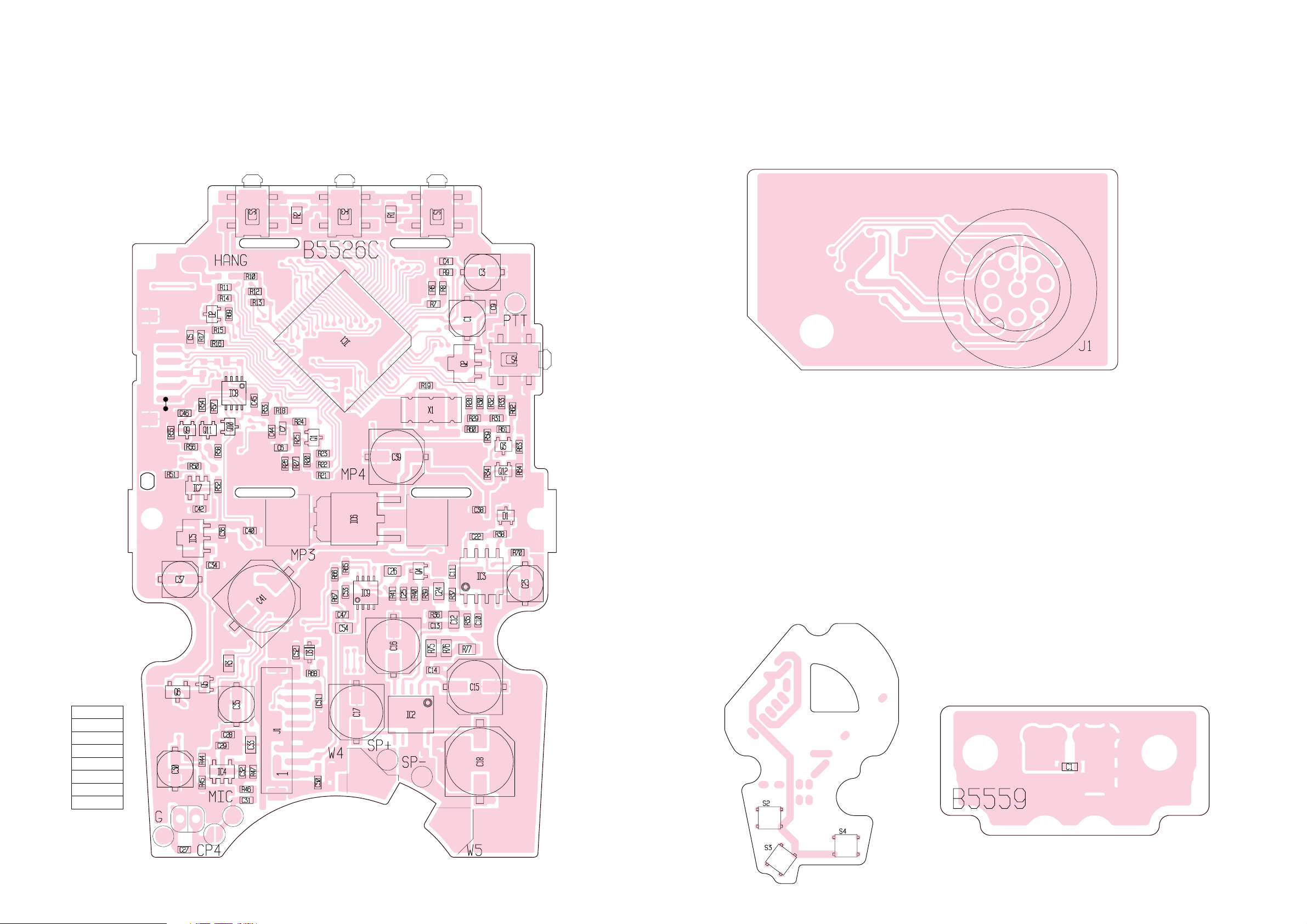
9 - 7
• BOTTOM VIEW (HM-127)
1
40
41
60
61
85
41
51
106
41
85
80
1
2021
4
58
RRXDA
PWRC
RTXDA
PTTC
GND
MICG
AF/MIC
VCC
1
8
to IC-M502
CTRL unit J1
J1
• BOTTOM VIEW (CTRL)
• BOTTOM VIEW (HM-126) • BOTTOM VIEW (PWR-CORD)
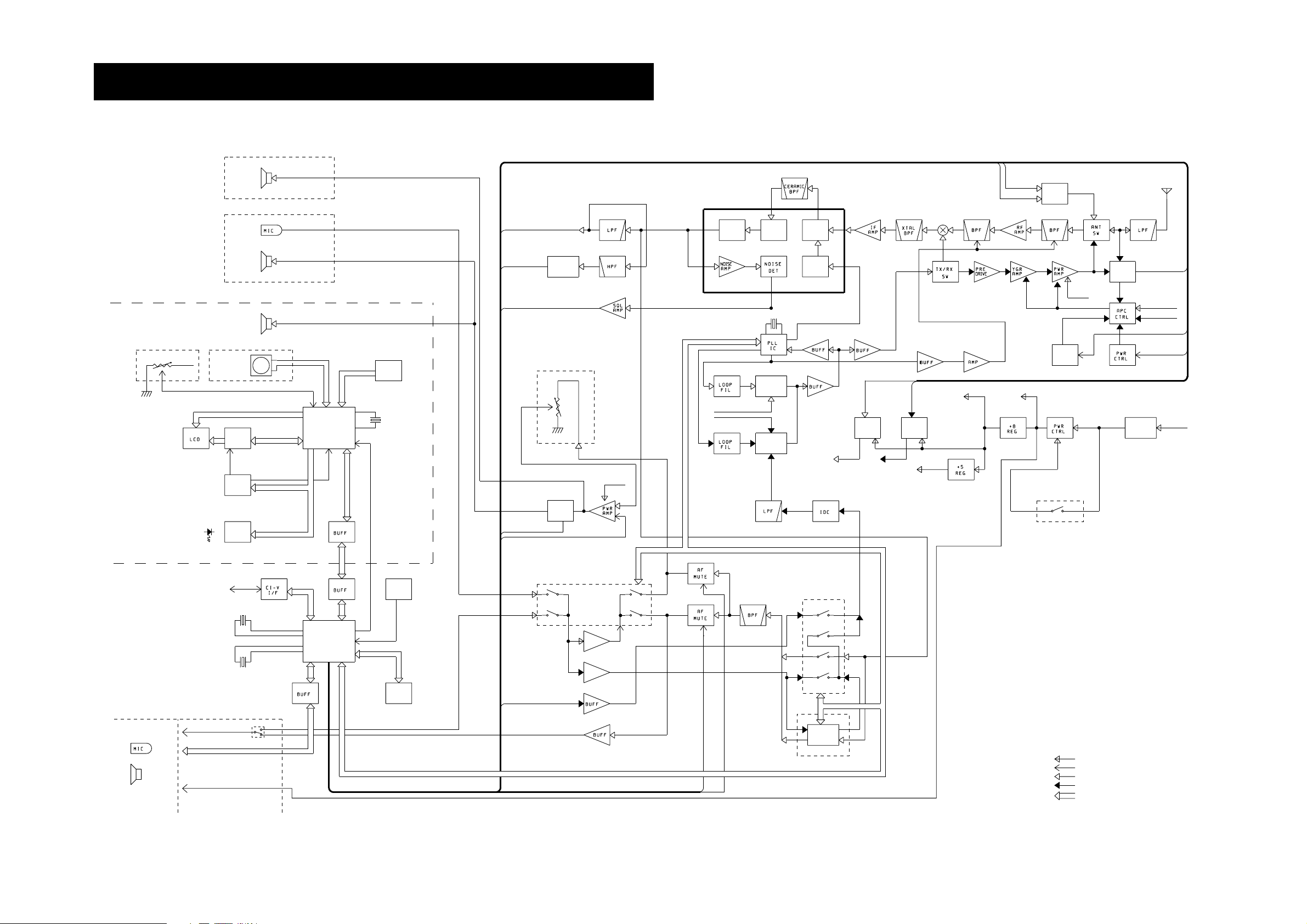
10 - 1
SECTION 10 BLOCK DIAGRAM
ANT
Q31 DTC144EU
Q32 2SC4116
ATTB
ATTA
IC1
TA31136FN
FI3
ALFY450E
EXT.SP
OPTION
EXTERNAL SPEAKER
LOGIC UNIT
SPEAKER MIC
HM-126
SP
MIC
SP
WX ALERT
DSC DEC
SQL
IC4B
NJM4558M
IC4A
NJM4558M
IC20
NJM2125F
IC5 NJM2211M
IC6 TC7W14FU
DSC
DECODER
RF
MUTE
AMP
FM
DET
2nd
MIX
2nd Lo
BUFF
2nd IF
21.25 MHz
X2
CR-659
SQLI
Q4
2SC2714
Q3
3SK166
D11, D12
MA77
FI1, FI2
FL-310
1 stage3 stage
ATT
VCC
TX
MUTE
CTRL
Q11
2SC3775
Q12
2SC2954
IC3
SC-1302
RF OUT
DET
Q2
3SK292
D16, D17
XB15A308
Q14 2SB1143
Q16 FMW1
Q18 2SC4116
D14, D15 HSM88ASR
VCC
T5
TXDET
13.8V
HI/LO
TMUT
D19
DSA3A1
REVERSE
CONNECT
PROTECT
VCC8V
Q17
DTC144EU
Q15
DTC144EU
IC8
TA7808S
RL1
FTR-F3AA012E
RCV
SEND
Q10
2SC4215
Q20 2SB1132
Q21 DTC144EU
Q22 2SB1132
Q23 DTC144EUR8CTRL
TX-VCO
RX-VCO
T8
CTRL
T8
R8
Q5
2SC4215
Q9
2SC4215
IC2
µPD3140GS
Q8 2SK210
D9, D10 MA363B
AF
VR
VOL UNIT
X1
4.91 MHz
SQLV
SUB MPU
KEY
BOARD
DIAL UNIT
IC2
HD66712SA03FS
IC1
µPD789405AGK-A30-9EU
D5V
ENCODER
SQL UNIT
DS1
Q1, Q4
2SK1069
LCD
CONT
LCD
DRIVER
DIM
CTRL
Q2 2SC4116
Q3 2SB1132
Q8 2SC4116
DS2–DS17
SML-311YT
Q5
DTA144EU
Q6
DTC144EU
SRESET
VCC
SP
Q32 2SC4116
D23 1SS355
RL2 FTR-F3AA012E
IC14
LA4425A
IC13B
NJM4558M
Q7 2SK210
D6–D8 MA363B
R8 T8
A5V
IC13A
NJM4558M
IC9
TA7805F
HVHVS
LOGIC UNIT
Q26
2SJ144
Q27
2SJ144
IC12
BU4066BCF
Q24,25
2SC4116
SCRAM
UNIT
MIC
BEEPM
IC10
BU4066BCF
IC11B
NJM4558M
IC15
S-80928ANMP
RESET
MAIN MPU
CLONE
Q37 DTC144TU
D24 DA204U
X3
DMX-26S
32.768 kHz
Q35 DTA144EU
Q36 DTC144TU
IC16
MB90F583BPFV-G
MAIN UNIT
OPTION
CTRL UNIT
X4
CR-610
7.9872 MHz
PTTC/EXTRXD/EXTTXD
IC1
TC4W53F
AF/MIC
PWRC/ICF3
VCC
HM-127
IC18 TC7W14FU
Q40 2SK1069
IC17
HN58X2464TI
EEPROM
AMP
MIC
AMP
DSC
IC11A
NJM4558M
Q33
2SK1069
Q28
2SK1069
RMUTS
RMUTM
COMMON LINE
OPTION
LINE
RX LINE
TX LINE
DATA BUS LINE
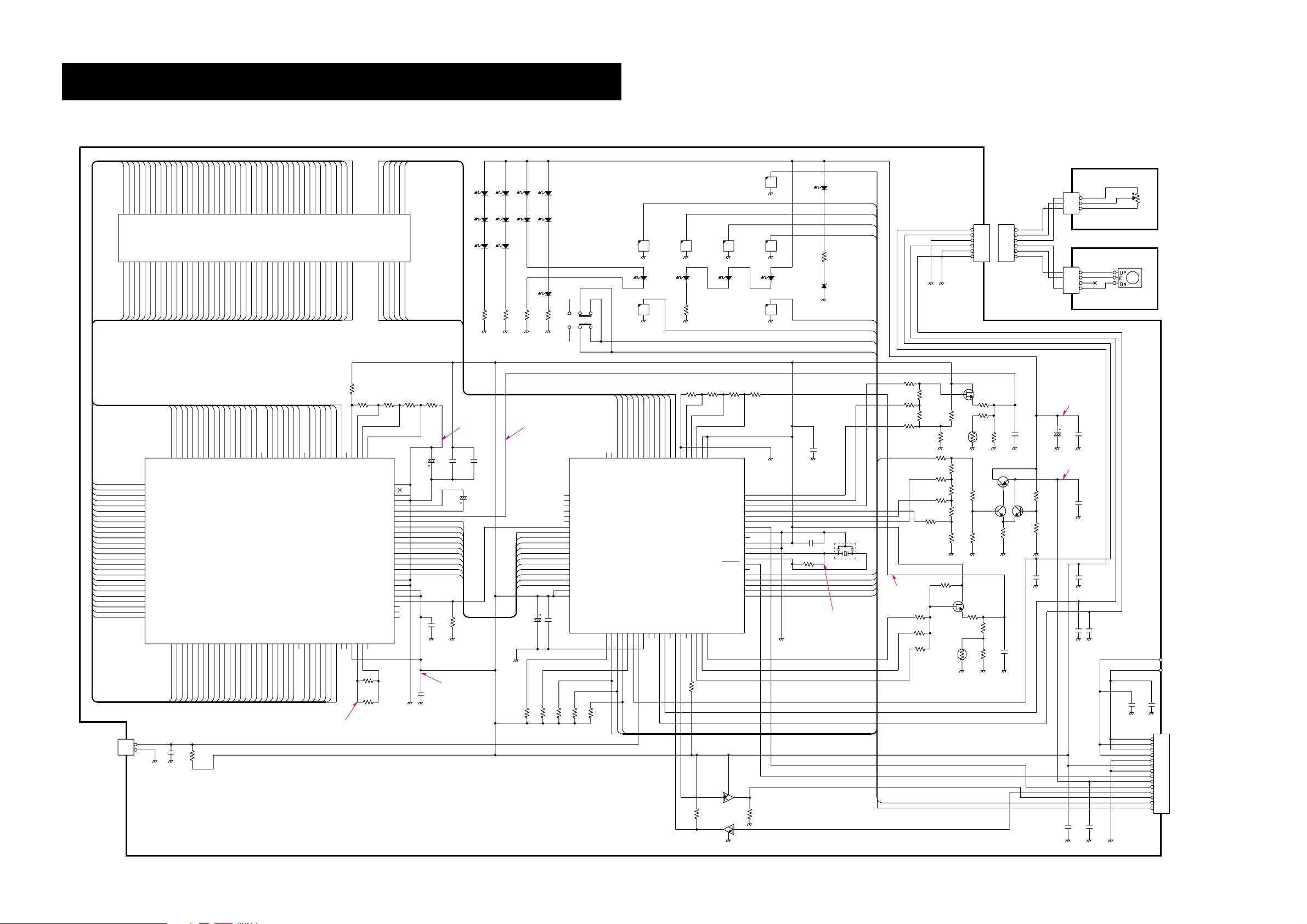
11 - 1
SECTION 11 VOLTAGE DIAGRAM
11-1 LOGIC UNIT
DS2
SML-311YT
SCAN
DSC
DTRS
DISTRESS
DS11 DS9 DS7
DS12 DS10 DS8
DS16
DS15
DS1
TSD0393
R53
220
DS14
POWER SW
H/L
DSC
R42
220
R43
220
+5V
DS13
S1
SPPH22014A
DS6
DS17
IC
SCAN CH/WX 16
R41
220
DS4DS3
DS5
D1
MA8043
R38
220
IC
CHWX
CH16
C12
0.001
C11
10
C9
0.1
R9
NTCCM16084BH
R10
10k
R8
10k
R7
1.5k
Q1
2SK1069
R1
47k
R3
47k
R5
47k
R2
10k
R4
10k
R64
33k
R6
12k
HL
HV
HVS
+5V
R27
10k
R28
10k
R29
10k
R30
10k
R45
10k
R46
27k
R47
10k
R48
10k
R44
10k
SEG18
103
SEG43
128
CL2
39
V5
64
D
40
M
41
RESET
42
IM
43
EXT
44
TEST
45
GND
46
RS/CS
47
RW/SID
48
E/SCLK
49
DB0/SOD
50
DB1
51
DB2
52
DB3
53
DB4
54
DB5
55
DB6
56
DB7
57
VCI
58
C2
59
C1
60
GND
61
V5OUT2
62
V5OUT3
63
SEG19
104
SEG20
105
SEG21
106
SEG22
107
SEG23
108
SEG24
109
SEG25
110
SEG26
111
SEG27
112
SEG28
113
SEG29
114
SEG30
115
SEG30
116
SEG32
117
SEG33
118
SEG34
119
SEG35
120
SEG36
121
SEG37
122
SEG38
123
SEG39
124
SEG40
125
SEG41
126
SEG42
127
IC2
HD66712SA03FS
SEG18
SEG19
SEG20
SEG21
SEG22
SEG23
SEG24
SEG25
SEG26
SEG27
SEG28
SEG29
C22
1
C20
0.1
C19
0.01
C21
1
DB7
DB6
DB5
DB4
DB3
P40/KR0
80
S10
21
AVREF
40
P03
61
S11
22
S12
23
S13
24
S14
25
S15
26
P93/S16
27
P92/S17
28
P91/S18
29
P90/S19
30
P87/S20
31
P86/S21
32
P85/S22
33
P84/S23
34
P83/S24
35
P82/S25
36
P81/S26
37
P80/S27
38
AVDD
39
P02
62
P01
63
P00
64
P47
65
P46
66
RESET
67
X2
68
X1
69
VSS0
70
VDD0
71
XT2
72
XT1
73
IC
74
P45/KR5
75
P44/KR4
76
P43/KR3
77
P42/KR2
78
P41/KR1
79
IC1
µPD789405AGK-A30-9EU
E
RW
RS
C15
0.01
C16 0.01
X1
CSTCC4.91MG
R16
10k
R14
10k
R12
10k
R15
20k
R67
18k
R68
10k
R11
20k
R13
18k
CONTDOT1
CONTDOT2
CONTDOT3
DIM1
DIM2
DIM3
+5V
DIM4
Q3
2SB1132
C13
0.01
R17
1k
Q2
2SC4116
R69
39k
Q8
2SC4116
R55
10k
R56
3.3k
R70
47k
8V
to Internal
Speaker
to MAIN
unit J4
J3
DIALA
DIALB
GND
SQLV
SQLG
+5V
C5
0.001
C4
0.1
C3
0.1
R25
NTCCM16084BH
R26
10k
C14
0.1
R24
10k
R23
1.5k
C6
0.001
Q4
2SK1069
R22 10k
R18
100k
R19
47k
R20
22k
R65 1M
HL
DSC
IC
DTRS
SQLV
DIALA
DIALB
+5V
VPP
SRESET
LMDA
DIM4
C1710C18
0.01
DB7
DB6
DB5
DB4
DB3
DB2
DB1
DB0
+5V
C23
0.01
R49
100k
DB2
DB1
DB0
E
RW
RS
SEG30
SEG31
SEG32
SEG33
SEG34
SEG35
SEG36
SEG37
SEG38
SEG39
SEG40
SEG41
SEG42
SEG43
1
2
J1
to HM-126
J2
C25
0.01
R52
10k
KEYM
C24
0.1
R51
120k
R50
390k
R33
100k
R34
100k
R35
100k
R36
100k
R37
100k
R66
100k
CONTSEG1
CONTSEG2
CONTSEG3
C1
0.001C20.001
1
2
3
4
5
6
7
8
9
10
11
12
13
14
J4
SP–
GND
SP+
SP–
SP+
SP+
SP–
+5V
GND
SRESET
8V
HV
HVS
LMDA
VPP
MLDA
C7
0.01
C8
0.01
HV
HVS
Q5
DTA144EU
R31
10k
R32
10k
Q6
DTC144EU
SQL UNIT
R1
S1
DIAL UNIT
DIALB
GND
DIALA
SQLV
1
2
3
J1
1
2
3
4
J2
SQLG
SQL5V
DIALA
GND
DIALB
SQLV
SQLG
SQL5V
1
2
3
4
5
6
W1
LOGIC UNIT
DS3–DS17
SML-311YT
1
2
3
4
5
6
COM15
COM14
COM13
COM12
COM11
COM10
COM9
SEG6
SEG7
SEG8
SEG9
SEG10
SEG16
SEG17
SEG18
SEG19
SEG20
SEG26
SEG27
SEG28
SEG29
SEG30
SEG36
SEG37
SEG38
SEG39
SEG40
SEG46
SEG47
SEG48
SEG49
SEG50
SEG56
SEG57
SEG58
SEG59
SEG60
COM1
COM2
COM3
COM4
COM5
COM6
COM7
LS0
LS1
LS2
LS3
LC2
LC3
COM17
COM18
COM19
COM20
COM21
COM22
COM23
SEG1
SEG2
SEG3
SEG4
SEG5
SEG11
SEG12
SEG13
SEG14
SEG15
SEG21
SEG22
SEG23
SEG24
SEG25
SEG31
SEG32
SEG33
SEG34
SEG35
SEG41
SEG42
SEG43
SEG44
SEG45
SEG51
SEG52
SEG53
SEG54
SEG55
COM31
COM30
COM29
COM28
COM27
COM26
COM25
LS4
LS5
LS6
LS7
LC0
LC1
C15
C14
C13
C12
C11
C10
C9
S06
S07
S08
S09
S10
S16
S17
S18
S19
S20
S26
S27
S28
S29
S30
S36
S37
S38
S39
S40
S46
S47
S48
S49
S50
S56
S57
S58
S59
S60
C1C2C3C4C5C6C7
LS0
LS1
LS2
LS3
LC2
LC3
C17
C18
C19
C20
C21
C22
C23
S01
S02
S03
S04
S05
S11
S12
S13
S14
S15
S21
S22
S23
S24
S25
S31
S32
S33
S34
S35
S41
S42
S43
S44
S45
S51
S52
S53
S54
S55
C31
C30
C29
C28
C27
C26
C25
LS4
LS5
LS6
LS7
LC0
LC1
12345678910111213141516171819202122232425262728293031323334353637383940414243
44
4546474849
50
51525354555657585960116263646566676869707172737475767778798081828384858687888990919293
94
9596979899
100
SEG17
102
101
10099989796959493929190898887868584838281807978777675747372717069686766
65
SEG17
SEG16
SEG15
SEG14
SEG13
SEG12
SEG11
SEG10
SEG9
SEG8
SEG7
SEG6
SEG5
SEG4
SEG3
SEG2
SEG1
COM0
COM1
COM2
COM3
COM4
COM5
COM6
COM7
COM17
COM8
COM18
COM19
COM20
COM21
COM22
COM23
COM24
V1V2V3
V4
SEG16
SEG15
SEG14
SEG13
SEG12
SEG11
SEG10
SEG9
SEG8
SEG7
SEG6
SEG5
SEG4
SEG3
SEG2
SEG1
COM1
COM2
COM3
COM4
COM5
COM6
COM7
COM17
COM18
COM19
COM20
COM21
COM22
COM23
SEG44
SEG45
SEG46
SEG47
SEG48
SEG49
SEG50
SEG51
SEG52
SEG53
SEG54
SEG55
SEG56
SEG57
SEG58
SEG59
SEG60
COM9
COM10
COM11
COM12
COM13
COM14
COM15
COM16
COM25
COM26
COM27
COM28
COM29
COM30
COM31
COM32
COM33
VCC
OSC2
OSC1
CL1
SEG44
SEG45
SEG46
SEG47
SEG48
SEG49
SEG50
SEG51
SEG52
SEG53
SEG54
SEG55
SEG56
SEG57
SEG58
SEG59
SEG60
COM9
COM10
COM11
COM12
COM13
COM14
COM15
COM25
COM26
COM27
COM28
COM29
COM30
COM31
123456789
1011121314151617181920212223242526272829303132333435363738
20
S9S8S7S6S5S4S3S2S1
S0
COM3
COM2
COM1
COM0
LS7
LS6
LS5
LS4
LS3
LS2
LS1
LS0
LC3
LC2
LC1
LC0
VSS1
VLC2
VLC1
VLC0
BIAS
VDD1
19181716151413121110987654321
P66/ANI6
P65/ANI5
P64/ANI4
P63/ANI3
P62/ANI2
P61/ANI1/CMPREF
P60/ANI0/CMPIN0
AVSS
P27/INTP3/CPT5
P26/INTP2/TO5
P25/INTP1/TI1
P24/INTP0/TI0
P23/CMPTOUT0/TO
P22/SI/RXD
P21/SO/TXD
P20/SCK/ASCK
P53
P52
P51
P50
414243
SCAN
CHWX
CH16
4445464748495051525354
55
SQLV
KEYM
DIALB
DIALA
SRXD
STXD
5657585960
-
1.89V 1.94V
5.06V
289kHz
4.9Vp-p
4.93MHz
5.1Vp-p
3.73V
7.95V
8.02V

11 - 2
11-2 MAIN UNIT
1
2
3
4
5
6
7
8
9
10
11
12
13
14
J2
PWRC/ICF3
GND
MDDA
DMDA
MCDA
J1
1
TC4W53F
IC1
2
3
4
8
7
6
5
D5V
SMIC
SAFO
PTTC
1
C11
1
C12
C13 1
GND
5
7
4
3
1
8
2
6
VCC
AF/MIC
MICG
EXTRXD
PWRC/ICF3
EXTTXD
PTTC
+5V
VCC
VCC
DSCMODDSCMOD
SAFO
GND
SMIC
MICG
CMDA
RESET
R19
10
C31
47p
C32
0.022
C33
0.001
R22
1.5k
R23
100k
330
R304
C40
0.001
R25
3.3k
C42
0.022
C43
0.001
R20
2.2k
L34
1µ
DEMOD
C39
0.01
Q4
2SC2714
C48
0.22
C49 0.1
IC1
TA31136FN
C50
0.001
R26
470
C51
0.001
C52
0.1
C53
100p
X1
CDBCA450CX24
R27
1.2k
R28
390
C54
47p
C55
0.01
R29
1.5k
D5
MA8036
C56
10
C57
0.01
R8
CP3
C65
0.001
R35
68k
R36
680
L8
0.1µ
C66
5p
Q5
2SC4215
C67
20p
R37
100
R39
100
C68
0.001
R40
47
R38
68
C303
0.001
VCC1
1
IN1
2
ENB
3
CLK
4
DATA
5
T1
6
LOK
7
CP1
8
FI1
9
FO1
10
FO2
11
FI2
12
CP2
13
GND2
14
XO
15
XI
16
XB
17
VCC2
18
IN2
19
GND1
20
IC2
µPD3140GS
VCC
R8
8V
VCC
T8
+5V
8V
+5V
C79
0.022
Q42
DTA144EU
R246
100k
OPTIN
HANG
ATTA
ATTB
ATT2
MAIN BUS
PLL BUS
OPT BUS
VCC
TAUX3
TMODE
R199 100k
R200
100k
Q41
DTA144EU
RMUTM
RCV
RMUTS
ATT1
VCC
R182
39k
R183
39k
C248 0.027
R184 100k
R185 100k
OUT
1
VDD
2
VSS
3
NC
4
CD
5
IC15
S-80928ANMP
TAUX3
TMODE
R186
100k
R188
47k
R305
47k
C251
24p
X4
CR-610
C252 24p
R189
1M
R190 10
R191
100k
R192
2.7k
C253 0.1
P71
26
HSTK
50
PA2
76
P21/A17
100
P72
27
DVRH
28
DVSS
29
P73/DA00
30
P74/DA01
31
AVCC
32
AVRH
33
AVRL
34
AVSS
35
P50/AN0/SIN3
36
P51/AN1/SOT3
37
P52/AN2/SCK3
38
P53/AN3
39
VSS
40
P54/AN4/SIN4
41
P55/AN5/SOT4
42
P56/AN6/SCK4
43
P57/AN7
44
P80/IRQ0
45
P81/IRQ1
46
MD0
47
MD1
48
MD2
49
X1A
77
X0A
78
VSS
79
X0
80
X1
81
VCC
82
P00/AD00
83
P01/AD01
84
P02/AD02
85
P03/AD03
86
P04/AD04
87
P05/AD05
88
P06/AD06
89
P07/AD07
90
P10/AD08
91
P11/AD09
92
P12/AD10
93
P13/AD11
94
P14/AD12
95
P15/AD13
96
P16/AD14
97
P17/AD15
98
P20/A16
99
IC16
MB90587CA-107
R193
27k
DATAM
DATAS
R201
100k
R202 100k
R203 100k
R45
1k
C81
0.01
R204
150k
C254
0.01
R205
47k
R253
8.2k
C294
2.2
UNLK
PSTB
UNLK
DSDEC
TXDET
WXDEC
LBAT
SQL
RTXD
RRXD
PTT
BE
CK
DATA
MDDA
DATAS
C69
18p
X2
CR-659
C70 10p
C71 12p
R41 330
R42
47k
R289
3.3k
C72
0.001
C74
0.001
R43 1k
Q6
2SK880
R44
10k
C283
0.001
R248 47k
R249
33k
R256
18k
R254
560
C293
0.1
R255
1k
C77 0.001
Q7
2SK210
C285
0.001
Q44
2SC4116
C286
0.1
R261
4.7k
R250
47
D29
1SS355
C295
0.047
CP2
C58
0.001
1 2
345
FI3
ALFY450E
C59 0.1
C60 0.001
C62 1
R30
330k
C63
220p
C64
220p
R32
33k
C103
0.001
R63
2.2k
C102
0.001
R33
20k
R31
820
R283
NTCCM16084LH
R8
HVS
HV
+5V
SMIC
SAFO
+5V
MOD
SP
-
SP+
R18
10k
R21
1.2k
FI1
FL-310
FI2
FL-310
C38
0.001
C45
39p
L7
56n
C47
0.001
Q3
3SK166
R241
180
C46
39p
C274 0.001
C34
0.001
C36 6p
C312 0.01
L30
0.15µ
CP1
IC21
NJM2125F
R72
100
C110
0.001
C111
0.001
R73
10
R292
R290
120k
27k
L18
82n
C112
1p
Q12
2SC2954
R74 1k
C114
0.001
C335
0.01
C331
0.01
C115
6.8
C116
22p
C117
18p
L19
47n
C118
39p
L20
47n
C119
18p
R75 10
C113 0.001
C96
0.001
C97
0.01
C98
12p
R57
100
R58
100
R60
2.2k
L16
0.1µ
Q10
2SC4215
R61
220
C99 0.001
C100
0.001
C101
12p
D11
MA77
D12
MA77
R62
1k
R64
39
R65
2.2k
R66
390
C104
0.001
C105
0.001
R67
10k
R68
10k
L17
82n
Q11
2SC3775
C107 0.001
R70
10
C108
0.001
C109
18p
R71
1k
R291
47k
D13
1SS355
R59
3.3k
C106
47p
R69 100
T8
R55
68k
L15
0.1µ
Q9
2SC4215
R56
680
C278
0.001
L12
3.9µ
D10
MA363B
D9
MA363B
L13
LB-257
C297 1p
C298
2p
C299
4p
Q8
2SK210
L14
2.7µ
R258
1k
L9
3.3µ
D7
MA363B
D6
MA363B
D8
MA363B
C284 1p
L10
LB-258
C287 7p
C288
4p
C289
3p
C290
0.5p
C291
0.5p
L11
2.7µ
Q45
2SC4116
R262
2.2k
R251
82
C304
0.22
R259
10
C305
0.22
C302
0.75p
R270
5.6k
C301
0.1
C300
0.001
C314
10
R276
47
C318
10
R209 1k
Q33
2SK1069
R212
2.7k
R252
4.7k
C292
0.22
R257
1k
C296
0.047
DSC
MICDSC
BE
BAND EXTENTION
+5V
R208
100k
C255
0.1
C256
10
C257
0.1
R210
1M
R211
56k
R225 47k
R226 47k
C259
0.1
A0
1
A1
2
A2
3
VSS
4
VCC
8
GND
7
SCL
6
SDA
5
IC17
HN58X2464TI
STRU
SCON
R194
100k
STRU
SCON
OPSTB
PSTB
PTTM
SRESET
CK
DATA
P01
ATT1
ATT2
Q34
DTA144EU
R218 10k
R219 100k
R220 100k
R221 100k
R222 100k
470
R237
NMEAI+
NMEAI
-
R224
100k
PTTS
MMUTE
SMUTE
SP
HI/LO
SEND
/TMUT
MLDA
LMDA
R223
100k
Q35
DTA144EU
Q36
DTC144TU
C258
0.1
R227
15k
Q37
DTC144TU
R2281kR229
1k
D24
DA204U
ICF3
RRXD
+5V
UART BUS
RTXD
CMDA
D26
HSU88
D27
1SS355
R233
1k
R234
47k
C262
0.1
R236
6.8k
1
2
3
45
6
7
8
IC18
TC7W14FU
R235
1k
R238
100k
R230
4.7k
Q40
2SK1069
for FLASH
+5V
TAUX3
GND
TMODE
TRES
GND
P01
SOT0SIN0
SCK0
12
34
56
78
910
J1
P01
TAUX3
TMODE
RESET
MCDA
CMDA
1
2
3
4
5
6
7
8
9
10
11
12
13
14
J3 W5
W6
ICF3
GND
+5V
VCC
VCC
SAFO
GND
SMIC
MICG
MDDA
DMDA
C9
0.01
C7
0.01
C15
0.01
D4
MA8062
C14
0.01
R239
100k
Q38
2SC4081
Q39
2SA1576
D28
DAP202U
R240
100k
R1
100k
R2
100k
R41MR5
1M
R6
100k
1M
R3
C306
0.1
C263
0.0047
R231
47
ICF3
MCDA
CMDA
MDDA
MCDA
DATAS
SRESET
MLDA
LMDA
from
LOGIC
unit J4
EXT-GPS
SP
-
SP
-
HVS
HV
LMDA
MLDA
VPP
1
2
3
4
5
6
7
8
9
10
11
12
13
14
J4
1
2
J2
GND
SP+
SP+
GND
SRESET
+5V
8V
CTRL UNIT
MAIN UNIT
RSTX
PA1
PA0
P97/POT
P96/PWC
P95/TOT2/OUT1
P94/TOT1/OUT0
P93/TOT0/IN3
P92/TIN2/IN2
P91/TIN1/IN1
P90/TIN0/IN0
RX*
TX*
P65/CKOT
P64/PPG0
P63/PPG1
P62/SCK2
P61/SOT2
P60/SIN2
P87/IRQ7
P86/IRQ6
P85/IRQ5
P84/IRQ4
P83/IRQ3
P82/IRQ2
75747372717069686766656463626160595857565554535251
BPLVLM
BEEPM
FLASH BUS
P22/A18
P23/A19
P24/A20
P25/A21
P26/A22
P27/A23
P30/ALB
P31/RDK
VSS
P32/WRLX
P33/WRHX
P34/HRQ
P35/HAKX
P36/RDY
P37/CLK
P40/SIN0
P41/SOT0
P42/SCK0
P43/SIN1
P44/SOT1
VCC
P45/SCK1
P46/ADTG
P47
C
123456789
101112131415161718192021222324
25
OPSTB
PSTBCKDATA
PTTM
PTTS
MMUTE
SMUTESPHI/LO
SEND
TMUT
SRXD
STXD
TCK
CLRX
CLTX
CLRX
CLTX
8VT8R8
VCC
SQLI
AFOUT
QUAD
IFOUT
RSSI
N_DET
N_REC
GND
MIXIN
9101112131415
16
FILIN
FILOUT
DEC
IFIN
VCC
MIXOUT
OSCOUT
OSCIN
8765432
1
VCC8V+5V
MAIN (2)
4
1
3
2
5
C10
10
TLP121
IC19
EXTMIC PTT ON :0V
EXTMIC PTT OFF:4.95V
13.2V
4.95V
2.46V
4.71V 21.25MHz
21.7MHz
RX : 3.03V
TX : 0V
RX : 0V
TX : 7.95V
RX : 0.3V
TX : 13.2V
MAIN (1)
BUS LINE
SQLI
R8
c
d
VCC
T8
VGG
PI
HVS
HV
+5V
MAIN BUS
OPT BUS
SMIC
SAFO
+5V
MOD
SP
-
SP+
DEMOD
R8
T8
+5V
8V
VCC

11 - 3
GND
VOL1
VOL2
R1
TP96N97-15F10KA-2345
GND
1
2
3
J1
to LOGIC
W2
CHASSIS
J2
C1
18p
W2
C7
0.001
C9
0.001
L2
LS-440
R3
33k
R5
10k
R8
470
R287 1
R7
100
R277
R1D31
39MA77
C10
0.001
C21
0.5p
W5W6
CP5
C26
0.01
C27
0.001
C22
2p
R263
10k
C307
0.22
1
3
2
4
5
IC20
NJM2125F
C308
0.1
R266
1k
R267
10k
R265
10k
R264
10k
R268
1k
C309
0.22
C315
C275
HVS
HV
+5V
HVS
HV
+5V
T8
VCC
C23 2p
C332
1p
C24
15p
D4
1SV214
R12
220k
R288
10k
1k
R297
C25
0.001
C330
0.001
L4
LS-440
1234
IC3
SC-1302
R16
10k
C28
10p
R2
220k
C6
0.001
C8
470p
C11
0.001
C12
470p
C13
1.5p
C14
15p
D2
1SV214
D36
1SV214
D35
1SV214
D34
1SV214
R10
220k
C15
0.001
C16
3p
L3
LS-440
C18
15p
D3
1SV214
R11
220k
C19
0.001
C20 2p
R88
150
C132
0.001
L22
LW-25
L31
D16
XB15A308
C141
33p
L26
LA-243
C142
27p
D17
XB15A308
L27
LA-238
C143
100p
Q2
3SK292
R9
100
R6
47k
R4
22k
C17
0.001
L1
LS-440
C4
15p
D1
1SV214
C5
2p
C3
0.3p
C2
0.001
C1
0.001
ANT
PWR-CORD BOARD
VOL UNIT
R80
150
C126 0.001
C127
24p
R81
2.2k
L21
LA-243
R82
2.2k
C128
18p
C129
0.001
C130
0.001
D14
HSM88ASR
D15
HSM88ASR
R83
10k
R84
RV-143
R85
22k
R86
1M
Q17
DTC144EU
C131
0.001
R87
100k
Q18
2SC4116
C133
0.001
L23
LA-149
L24
LA-243
L25
LA-253
C1348pC136
12p
C137
5p
C138
27p
C139
4p
C120 220
C123 0.001
PI
VGG
VDD
P0
Q14
2SB1143
R76
47k
C124
1
Q15
DTC144EU
R77
5.6k
R78 3.3k
R79 10k
C125 0.01
345
12
Q16
FMW1
DEMOD
A5V
VCC
+5V
T8
RCV
R8
DEMOD
+5VR8DEMOD
8V
R90
47
R102
10k
C153
0.012
R103
10k
C154
0.033
C155
0.033
R104
10k
C156
470p
R95
100k
R96
100k
C148
0.1
5
6
7
IC4B
NJM4558M
C157
0.047
C159
0.22
R105
470k
R106
47k
V+
1
IN
2
LOCK
3
GND
4
Q
5
Q
6
DATA7FSK
8
NC
9
REF
10
LOOP
11
R
12
CAP
13
CAP
14
IC5
NJM2211M
C161
0.033
C162 0.1
R107
100k
C163
0.0022
R108
39k
R109
15k
C164
0.01
R110
RV-148
C158
0.1
C317
10
CP4
Q20
2SB1132
R112
10k
C166
0.001
R113
2.2k
Q21
DTC144EU
Q22
2SB1132
R114
10k
C167
0.001
R115
2.2k
Q23
DTC144EU
C17110C172
0.1
IC8
TA7808S
C175
10
C176
0.1
IC9
TA7805F
R116 47
8V
R8
VCC
+5V
+5V
+5V
HV
HVS
VCC
5V
C173
0.1
C174
10
C177
0.1
D18
1SS355
RL1
FTR-F3AA012E
C179 470
C178
0.01
D19 DSA3A1
HV
VCC
1
2
3
4
HV
J1
HV
HV
HV
GND
GND
C327
0.001
C326
0.01
GND
1
2
3
1
2
3
W1
GND
VOL1
HV
C202
47p
VOL2
VOL1
VBIAS
INCOM
MMIC
SMIC
MICAF
C194
0.1
R132 100k
R133
100k
Q28
2SK1069
C196
0.1
R134
1k
C197
0.001
I/O
1
O/I
2
O/I
3
I/O
4
CONT.B
5
CONT.C
6
VEE
7
I/O
8
O/I
9
O/I
10
I/O
11
CONT.D
12
CONT.A
13
VDD
14
IC10
BU4066BCF
R135
1M
R136
1M
C198
0.1
C199
0.1
C200
0.1
C328
C195
0.01
C192
1
C193
1
R280
10k
R285
100k
R281
820
R296
10k
R295
10k
R286
100k
R137R284
0.1
2.7k100k
OPT BUS
MAIN BUS
SAFO
5V
SMIC
R117 1k
C182
0.22
C183
0.027
C184
0.027
R119 8.2k
R120
560k
R121
180k
R122
2.7k
Q24
2SC4116
R123
330
R124
33k
R125
33k
C185
0.0022
C186
820p
Q25
2SC4116
R126
2.2k
R127
100k
Q26
2SJ144
R128
470k
C190
0.0039
Q27
2SJ144
R129
470k
2SJ144
Q46
C191
0.0039
R130
100k
R131
100k
R154
1M
R155
1M
C189
1
C188
10
R8
5V
SMIC
SAFO
C160
0.1
1
2
3
45
6
7
8
IC6
TC7W14FU
R111
330
C165
470p
R118
8.2k
DSC
STRU
R98
8.2k
C150
0.01
R99
1.5k
C151
0.01
R100
470k
R101
470k
3
2
1
4
8
IC4A
NJM4558M
R175
8.2k
C235
10
C236
0.1
R176
47
C246 0.22
C149
0.01
R97
10k
C152
0.01
DSDEC
+5V
+5V
SP
-
SP+
SMIC
SAFO
C282
0.1
C279
0.001
C229
47p
3
2
1
4
8
IC13A
NJM4558M
R164
100k
R165
150k
C225
0.001
R166
82k
C226
0.0039
R167
82k
C227
82p
R168
10k
C228
0.0027
R169
NTCCM16084BH
R170
12k
R171
12k
R173 18k
R174 33k
C232 10
C233 0.1
C234 0.01
5
6
7
IC13B
NJM4558M
C231 0.01
R172
RV-110
VBIAS
I/O
1
O/I
2
O/I
3
I/O
4
CONT.B
5
CONT.C
6
VEE
7
I/O
8
O/I
9
O/I
10
I/O
11
CONT.D
12
CONT.A
13
VDD
14
IC12
BU4066BCF
R156
1M
R157
56
R160
1M
C223
0.1
R161
12k
R162
82k
C224
22p
R163
1M
C239
1
C219
0.1
R300
10k
C319
0.1
BEEPM
BPLVLM
R147
1.2k
R294
100k
R148
18k
3
2
1
4
8
IC11A
NJM4558M
C215
470p
R149
39k
R150
18k
R151
1M
R152
1M
Q29
DTC144EU
R153
47k
C218
0.1
C217
0.01
MICDSC
VOL2
VCC
MICO
MICI
DETO
DETI
5V
+5V
VBIAS
R142
1M
C212
0.22
R143
15k
R144
18k
5
6
7
IC11B
NJM4558M
C213 47p
R145
1M
C214
0.033
C334
C333
0.1
1
OPTIN
OPSTB
SCON
CK
DATA
+5V
SCK
GND
SDATA
OPTIN
OPSTB
SCON
MICI
GND
DETI
GND
MICO
GND
DETO
Optional
unit
UT-98
or
UT-112
SP/MIC
J6
C203 0.1
C204 0.1
C205
0.1
PTT
HANG
MIC
GND
AF2
AF
AFG
EXT SP
MICE
AF1
SPMIC
HANDSET
C206
47p
C210
470p
1
2
3
4
5
6
7
8
J7
1
2
J8
C321
47p
R140 100
C207
0.001
R141 1k
C208
470p
C209
0.01
D20
DA204U
D21
DA204U
DAP202U
D38
PTT
HANG
RMUTM
PTTM
DAP202U
D37
Vcc
C242
0.1
C243
470
C244
470
R181
4.7
R301 R302 R303
330 330 330
C245
0.1
R260
18k
RL2
FTR-F3AA012E
D23
1SS355
Q32
2SC4116
Q47
2SC3326
AF1
AF
D22
DA204U
Q31
DTC144EU
R177
15k
R178
1.2k
C238
0.01
R179
1M
R180
22k
C241
0.001
1
2
3
4
5
IC14
LA4425A
C240
1
R247
22k
MOD
SQL
ATTA
R278
R242
22
D32
MA77
C316
0.001
0.001
C1 1p
C276
0.001
0.001
L32
2.2k
1µ
2.2k
1µ
ATTB
/TMUT
HI/LO
TXDET
WXDEC
SEND
+5VHVHVS
RCV
RMUTM
RMUTS
SMUTE
PTTS
PTTM
MMUTE
MICAF
DETISPDETO
MICI
MICO
GND
GND
ANT
MAIN (1)
C2
10p
D33
1SS375
C337
R299
R298
10
10k
10k
L33
10µ
3.48V
4.66V
4.95V
8.04V
13.8V
2.68V
2.68V
4.95V
MAIN (2)
BUS LINE
SQLI
R8
c
d
VCC
T8
VGG
PI
HVS
HV
+5V
MAIN BUS
OPT BUS
SMIC
SAFO
+5V
MOD
SP
-
SP+
DEMOD
R8
T8
+5V
8V
VCC

11 - 4
11-3 HM-127 (OPTIONAL UNIT)
J2
6
5
4
3
2
1
GND
RXD
TXD
RESET
VPP
5V
STXD
SRXD
RESET
VPP
5V 5V
SRXD
STXD
47k
R55
1k
R54
TC7W14FU
IC8
8
7
6
5 4
3
2
1
2SA1576
Q11
47
R58
4.7k
R57
RRXDA
PTT
0.1
C46
2SC4081
Q10
RTXDA
27k
R51
1k
R56
5V
0.01
C45
0.027
C42
2SK1069
Q9
S-80928ANMP
IC7
5
CD
4
NC
3
VSS
2
VDD
1
OUT
100k
R50
PTT
RMUTE
BEEP
RESET
VCCSW
0.1
C44
100k
R53
PTT
PWR
100k
R18
DOWN
UP
CONT3
CONT2
100k
R15
100k
R14
100k
R17
100k
R16
RMUTE
BEEP
100k
R10
100k
R13
100k
R12
100k
R11
0.01
C4
22
C3
SEG27
SEG26
SEG25
SEG24
SEG23
SEG22
SEG21
SEG20
CONT1
DIM4
1M
R19
SQL
IC
VOL
HL
39k
R61
10k
R60
10k
R29
10k
R31
10k
R33
20k
R32
18k
R30
20k
R28
15k
R59
2SC4116
Q3
PWR
2SC4116
Q12
3.9k
R64
10k
R63
47k
R62
0.1
C38
1k
R34
100
C39
330
C41
39k
R52
DAN202U
D2
0.1
C40
8V
CP18
CP16
CP14
100
R69
47p
C52
47p
C51
CP17
PWRC
RRXDA
RTXDA
MICG
AF/MIC
J1
PTTC
GND
VCC
100
R68
CP12
CP15
1
C54
1SS355
D3
TC4W53FU
IC9
8
7
6
5 4
3
2
1
1M
R67
0.001
C50
470P
C47
22
R77
22
R76
22
R75
CP11
VCC
0.1
C36
0.1
C34
TA78L05F
IC5
TA7808F
IC6
VCC5V
0.01
C9
2SB1132
Q2
10k
R27
NTCCM16084BH
R26
10k
R23
20k
R22
39k
R21
2SK1069
Q1
0.1
C7
1.2k
R24
10k
R25
VCCSW
VRDAT
VRCK
0.01
C5
CSTCC4.91MG
X1
0.01
C6
DIM3
DIM2
DIM1
µPD789405AGK-A30-9EU
IC1
79
P41/KR1
78
P42/KR2
77
P43/KR3
76
P44/KR4
75
P45/KR5
74
IC
73
XT1
72
XT2
71
VDD0
70
VSS0
69
X1
68
X2
67
RESET
66
P46
65
P47
64
P00
63
P01
62
P02
39
AVDD
38
P80/S27
37
P81/S26
36
P82/S25
35
P83/S24
34
P84/S23
33
P85/S22
32
P86/S21
31
P87/S20
30
P90/S19
29
P91/S18
28
P92/S17
27
P93/S16
26
S15
25
S14
24
S13
23
S12
22
S11
61
P03
P66/ANI6
P65/ANI5
P64/ANI4
P63/ANI3
P62/ANI2
P61/ANI1/CMPREF
P60/ANI0/CMPIN0
AVSS
WDSW
SCAN
CHWX
CH16
PWR
PTT
MODE
DOWNUPBEEP
STXD
SRXD
BPLVL
P27/INTP3/CPT5
P26/INTP2/TO5
P25/INTP1/TI1
P24/INTP0/TI0
P23/CMPTOUT0/TO
P22/SI/RXD
P21/SO/TXD
P20/SCK/ASCK
P53
P52
P51
P50
40
AVREF
21
S10
80
P40/KR0
SEG10
SEG19
SEG18
SEG17
SEG16
SEG15
SEG14
SEG13
SEG12
SEG11
10k
R7
10k
R6
10
C1
SKQLLC
S4
CP7
10k
R8
PTT
10k
R9
CH16
6.8k
R20
10KEY
S7
PTT
22
C37
0.1
C28
10
C30
AF5V
22
C35
5V
0.001
C29
DTC144EU
Q5
DTB123EK
Q6
100k
R45
0.01
C53
1M
R65
1M
R66
47p
C32
100k
R44
NJM2125F
IC4
5
4
2
1
3
MIC
CP6
MICG
SKB-2746 LPC
MC1
CP5
CP4
470k
R47
1
C33
1
C26
470p
C27
12k
R42
33k
R46
100k
R41
33
R70
22
C23
1
C24
2SJ144
Q4
0.01
C25
0.22
C31
0.01
C22
470k
R40
100k
R39
2.7K ERJ3GE
R43
M62429FP
IC3
8
VIN2
7
VOUT2
6
VCC
5
CLK
4
DATA
3
GND
2
VOUT1
1
VIN1
VOL
VRCK
VRDAT
15k
R38
DA204U
D1
DOWN
CHWX
IC
150
R3
SML-311YT
DS10
SML-311YT
DS9
10KEY
S11
10KEY
S8
10KEY
S9
10KEY
S6
SKQLLC
S3
SKQLLC
S2
120
R2
SKQLLC
S1
SEG21
SEG17
SEG13
COM3
COM2
COM1
COM0
SEG0
SEG1
SEG2
SEG3
SEG4
SEG5
SEG6
SEG7
SEG8
SEG9
SEG10
SEG11
SEG15
SEG19
MAIN UNIT
120
R1
FY1101F-TR
DS6
FY1101F-TR
DS5
A0119
DS1
SEG25
SEG23
SEG24
SEG20
SEG16
SEG12
SEG13
SEG14
SEG15
SEG17
SEG18
SEG19
SEG21
SEG22
SEG23
SEG25
SEG26
SEG27
SEG24
SEG20
SEG16
SEG12
SEG13
SEG14
SEG15
SEG17
SEG18
SEG19
SEG21
SEG22
SEG23
SEG25
SEG9
SEG8
SEG7
SEG6
SEG5
SEG4
SEG3
SEG2
SEG1
SEG0
COM3
COM2
COM1
COM0
S9S8S7S6S5S4S3S2S1
S0
COM3
COM2
COM1
COM0
VSS1
VLC2
VLC1
VLC0
BIAS
VDD1
SEG26
SEG27
SEG21
SEG17
SEG13
COM3
COM2
COM1
COM0
SEG0
SEG1
SEG2
SEG3
SEG4
SEG5
SEG6
SEG7
SEG8
SEG9
SEG10
SEG11
SEG15
SEG19
4567891011121314151617181920
3938373635343332313029282726252423
22
201918171615141312111098765432
1
41424344454647484950515253545556575859
60
21
321
FY1101F-TR
DS3
FY1101F-TR
DS2
SML-311YT
DS4
PWRSW
SCAN
HL
SML-311YT
DS7
SML-311YT
DS8
10KEY
S10
10KEY
S5
0.1
C11
1
C12
SQL
0.1
C10
10k
R36
22k
R37
1k
R35
UP
100
C16
TA7368F
IC2
10
POUT
9
PWGND
8
PREGND
7
PHASE
6
NF
5
RIPPLE
4
VIN
3
NC
2
VCC
1
NC
100
C15
0.1
C14
0.047
C13
100
C17
SP
-
SP+
+
-
SP1
036D0801
CHASSIS
CP2
CP3
330
C18
8
7
6
5
4
3
2
1

11 - 5
11-4 HM-126
1
2
P2
to LOGIC unit J1
(IC-M501EURO)
to MAIN unit J7
(IC-M501EURO)
KEYM
KGND
GREEN
BROWN
RED
BLACK
WHITE
GREEN
BROWN
W1 (CHASSIS)
IN
OUT
PTT
GND
MIC
SPMIC
KEYM
MICE
1
2
3
4
5
6
7
J1
KGND
1
2
3
4
5
6
7
P3
PTT
MIC
MICE
SPMIC
KEYM
UP-ON 2.0V
DN-ON 3.0V
H/L-ON 3.8V
GND
KGND
W1
W4
W3
R5 15
W2
C1
470p
C2
470p
R1
12k
SP1
S36G04K-4
MC1
KUC2123-030245
UP
PTT
DN
S1
SKHHLP014A
S2
S3
R2 6.8k
R3 15k
BLUE
HANG
SPMIC
GND
MIC
MICE
HANG
PTT
AF1
AF2
RED
BLUE
BLACK
WHITE
OUT
IN
1
2
3
4
5
6
7
8
P1
R4 33k
S4
S2–S4 : SKHHAM024A
H/L

Communication Equipment
Himmelgeister Str. 100, D-40225 Düsseldorf, Germany
Phone : 0211 346047 Fax : 0211 333639
URL : http://www.icomeurope.com
Unit 9, Sea St., Herne Bay, Kent, CT6 8LD, U.K.
Phone : 01227 741741 Fax : 01227 741742
URL : http://www.icomuk.co.uk
Zac de la Plaine, Rue Brindejonc des Moulinais
BP 5804, 31505 Toulouse Cedex, France
Phone : 561 36 03 03 Fax : 561 36 03 00
URL : http://www.icom-france.com
Crta. de Gracia a Manresa Km. 14,750
08190 Sant Cugat del Valles Barcelona, SPAIN
Phone : (93) 590 26 70 Fax : (93) 589 04 46
URL : http://www.icomspain.com
<
Corporate Headquarters
>
2380 116th Avenue N.E., Bellevue, WA 98004, U.S.A.
Phone : (425) 454-8155 Fax : (425) 454-1509
URL : http://www.icomamerica.com
<
Customer Service
>
Phone : (425) 454-7619
Glenwood Centre #150-6165
Highway 17 Delta, B.C., V4K 5B8, Canada
Phone : (604) 952-4266 Fax : (604) 952-0090
URL : http://www.icomcanada.com
A.B.N. 88 006 092 575
290-294 Albert Street, Brunswick, Victoria, 3056, Australia
Phone : 03 9387 0666 Fax : 03 9387 0022
URL : http://www.icom.net.au
146A Harris Road, East Tamaki,
Auckland, New Zealand
Phone : 09 274 4062 Fax : 09 274 4708
URL : http://www.icom.co.nz
6F No. 68, Sec. 1 Cheng-Teh Road, Taipei, Taiwan, R.O.C.
Phone : (02) 2559 1899 Fax : (02) 2559 1874
1-1-32, Kamiminami, Hirano-ku, Osaka 547-0003, Japan
Phone : 06 6793 5302
Fax : 06 6793 0013
URL : http://www.icom.co.jp/world/index.html
Icom America Inc.
Icom (Europe) GmbH
Asia Icom Inc.
Icom Spain S.L
Icom (UK) Ltd.
Icom France S.a
1305, Wanshang Plaza, Shijingshan Road, Beijing China
Phone : (010) 6866 6337 Fax : (010) 6866 3553
Beijing Icom Ltd.
Icom Canada
Icom (Australia) Pty. Ltd.
Icom New Zealand

1-1-32, Kamiminami, Hirano-ku Osaka 547-0003, Japan
S-13710HZ-CD-q
© 2000 Icom Inc.
 Loading...