HP INA-50311-TR1, INA-50311-BLK Datasheet

1 GHz Low Noise Silicon MMIC
Amplifier
Technical Data
INA-50311
Features
• Internally Biased, Single 5 V
Supply (17 mA)
• 19 dB Gain
• 3.6 dB NF
• Unconditionally Stable
SOT-143 Surface Mount Package
Applications
• Amplifier for Cellular,
Cordless, Special Mobile
Radio, PCS, ISM, Wireless
LAN, and TV Tuner
Applications
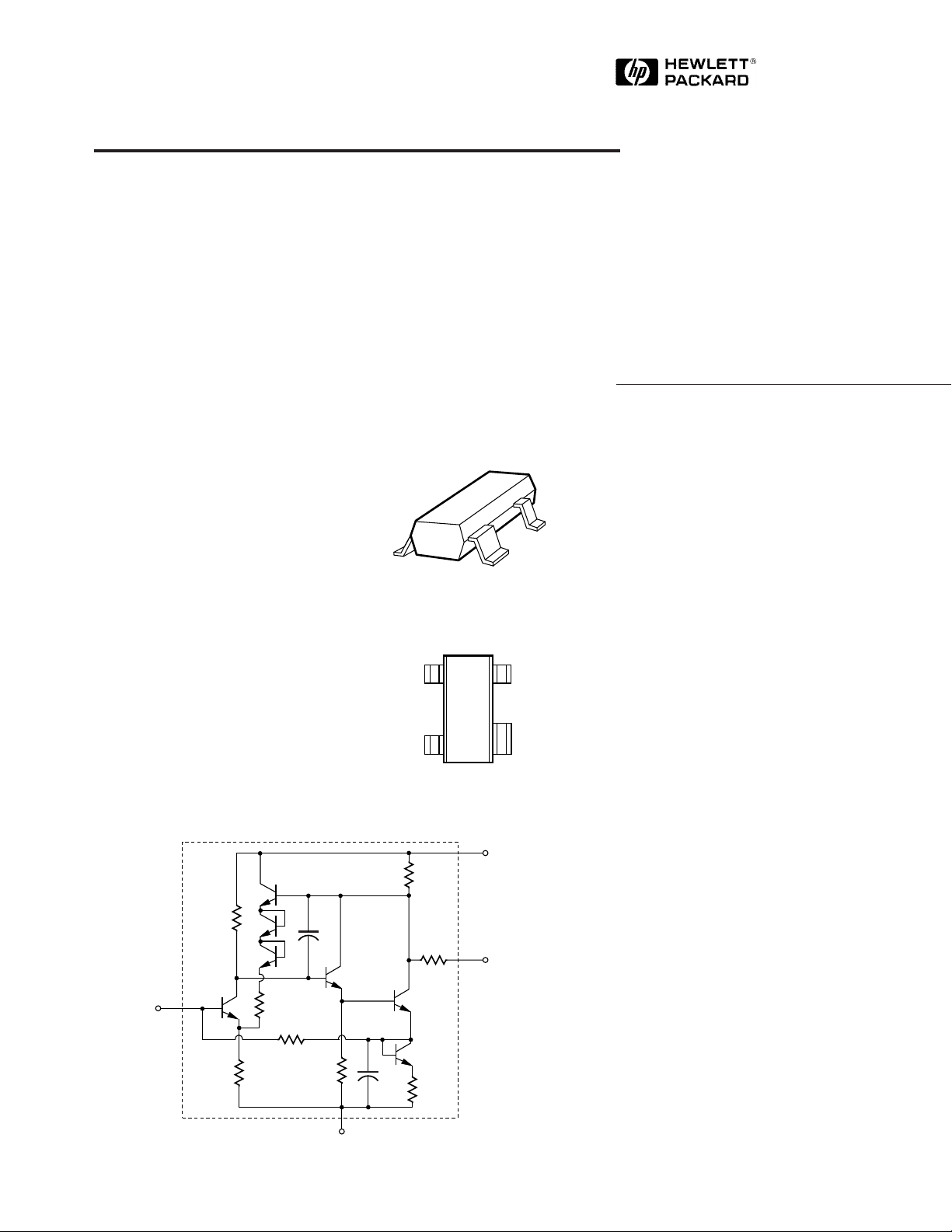
Pin Connections and Package Marking
Equivalent Circuit (Simplified)
INPUT
V
CC
N50
V
CC
GND
OUTPUT
Description
Hewlett-Packard’s INA-50311 is a
Silicon monolithic amplifier that
offers excellent gain and noise
figure for applications to 1.0 GHz.
Packaged in a miniature SOT-143
package, it requires very little
board space.
The INA-50311 uses a topology
which is internally biased,
eliminating the need for external
components and providing
decreased sensitivity to ground
inductance.
The INA-50311 is fabricated using
HP’s 30 GHz f
Silicon bipolar process which
uses nitride self-alignment submicrometer lithography, trench
isolation, ion implantation, gold
metallization, and polyimide
intermetal dielectric and scratch
protection to achieve superior
performance, uniformity, and
reliability.
MAX
ISOSAT
TM
RF
INPUT
5963-6680E
GROUND
RF
OUTPUT
6-146

Absolute Maximum Ratings
Absolute
Symbol Parameter Units Maximum
V
CC
P
in
T
j
T
STG
INA-50311 Electrical Specifications
Device Voltage, to ground V 12
CW RF Input Power dBm +13
Junction Temperature °C 150
Storage Temperature °C -65 to 150
[3]
, T
= 25°C, ZO = 50 Ω, V
C
[1]
Thermal Resistance
θ
= 550°C/W
jc
Notes:
1. Operation of this device above any one
of these limits may cause permanent
damage.
2. T
= 25°C (T
C
temperature at the package pins where
contact is made to the circuit board).
= 5 V
CC
is defined to be the
C
Symbol Parameters and Test Conditions Units Min. Typ. Max.
G
p
Power Gain (|S21|2) f = 900 MHz dB 16.5 19
NF Noise Figure f = 900 MHz dB 3.6
P
1dB
IP
3
Output Power at 1 dB Gain Compression f = 900 MHz dBm 0
Third Order Intercept Point f = 900 MHz dBm +10
VSWR Input VSWR f = 900 MHz 1.5
Output VSWR f = 900 MHz 1.2
I
cc
ι
d
Device Current mA 17 22
Group Delay f = 900 MHz ps 320
[2]
:
INA-50311 Typical Scattering Parameters
Freq. S
11
S
21
[3]
, T
= 25°C, ZO = 50 Ω, V
C
S
12
CC
= 5 V
S
22
GHz Mag Ang dB Mag Ang dB Mag Ang Mag Ang Factor
0.05 0.12 -2 22.2 12.82 -6 -31.9 0.025 5 0.08 -11 1.68
0.10 0.12 -5 22.2 12.81 -12 -31.7 0.026 9 0.07 -24 1.63
0.20 0.12 -10 22.1 12.80 -24 -31.4 0.027 16 0.07 -44 1.59
0.30 0.14 -16 22.1 12.68 -36 -31.1 0.028 23 0.08 -62 1.55
0.40 0.15 -25 21.9 12.45 -49 -30.6 0.030 30 0.09 -78 1.48
0.50 0.16 -32 21.7 12.12 -61 -30.0 0.032 36 0.09 -94 1.44
0.60 0.17 -45 21.3 11.65 -74 -29.3 0.034 42 0.10 -107 1.42
0.70 0.18 -57 20.9 11.04 -87 -28.5 0.038 47 0.11 -120 1.36
0.80 0.19 -71 20.3 10.35 -99 -27.7 0.041 51 0.11 -131 1.35
0.90 0.19 -84 19.6 9.57 -111 -26.9 0.045 54 0.11 -141 1.34
1.00 0.20 -98 18.9 8.78 -122 -26.0 0.050 56 0.11 -149 1.32
1.20 0.21 -122 17.2 7.28 -143 -24.3 0.061 59 0.11 -163 1.31
1.40 0.21 -143 15.5 5.97 -161 -22.8 0.072 60 0.11 -172 1.33
1.60 0.21 -162 13.8 4.92 -176 -21.5 0.084 60 0.10 -179 1.37
1.80 0.22 -177 12.2 4.08 169 -20.4 0.095 58 0.10 175 1.42
2.00 0.22 170 10.7 3.43 157 -19.5 0.106 55 0.10 172 1.49
2.20 0.21 158 9.3 2.92 145 18.5 0.119 54 0.10 166 1.55
2.40 0.20 149 8.1 2.53 134 -17.9 0.127 50 0.11 163 1.65
2.50 0.20 146 7.5 2.37 129 -17.7 0.131 49 0.12 160 1.69
Note:
3. Reference plane per Figure 9 in Applications Information section.
K
6-147
 Loading...