4.8 V NPN Common Emitter
Medium Power Output Transistor
Technical Data
AT-31625
Features
• 4.8 Volt Operation
• +28.0 dBm P
Typ.
• 70% Collector Efficiency
@␣ 900 MHz, Typ.
• 9 dB Power Gain @ 900 MHz,
Typ.
• -31 dBc IMD3 @ P
21␣ dBm per Tone, 900␣ MHz,
Typ.
• 50% Smaller than SOT-223
Package
@ 900 MHz,
out
of
out
Applications
• Medium Power Driver
Device for Cellular/PCS,
ISM 900, WLAN
• Output Power Device for
ISM 900, Cordless, WLAN
MSOP-3 Surface Mount Plastic Package
Outline 25
Pin Configuration
COLLECTOR
4
EMITTER 1 2
3 EMITTER
BASE
Description
Hewlett Packard’s AT-31625 is a
low cost, NPN medium power
silicon bipolar junction transistor
housed in a miniature, MSOP-3
surface mount plastic package.
The AT-31625 can be used as a
driver device or an output device,
depending on the specific application. The AT-31625 features
+28␣ dBm CW output power when
operated at 4.8 volts. Excellent
gain and superior efficiency make
the AT-31625 ideal for use in
battery powered systems.
The AT-31625 is fabricated with
Hewlett Packard’s 10 GHz Ft SelfAligned-Transistor (SAT) process.
The die are nitride passivated for
surface protection. Excellent
device uniformity, performance
and reliability are produced by the
use of ion-implantation, selfalignment techniques, and gold
metalization in the fabrication of
these devices.
4-43
5965-5911E

AT-31625 Absolute Maximum Ratings
Absolute
Symbol Parameter Units Maximum
V
EBO
V
CBO
V
CEO
I
C
P
T
T
j
T
STG
Emitter-Base Voltage V 1.4
Collector-Base Voltage V 16.0
Collector-Emitter Voltage V 9.5
Collector Current mA 320
Power Dissipation
[2]
W 1.0
Junction Temperature °C 150
Storage Temperature °C -65 to 150
[1]
Thermal Resistance
[3]
:
θjc = 65°C/W
Notes:
1. Permanent damage may occur if
any of these limits are exceeded.
2. Derate at 15.4 mW/°C for T
Tc is defined to be the temperature
of the collector pin 4, where the
lead contacts the circuit board.
3. Using the liquid crystal technique,
= 4.8 V, Ic= 50 mA, T
V
CE
1-2␣ µm “hot-spot” resolution.
> 85°C.
c
=150°C,
j
Electrical Specifications, T
= 25° C
C
Symbol Parameters and Test Conditions Units Min. Typ. Max.
Freq. = 900 MHz, VCE = 4.8 V, ICQ = 5 mA, CW operation, Test Circuit A,
unless otherwise specified
P
out
η
C
Output Power
Collector Efficiency
IMD33rd Order Intermodulation Distortion, 2 Tone Test, F1 = 899 MHz dB c -31
P
each Tone = +21 dBm
out
Mismatch Tolerance, No Damage
[1]
[1]
[1]
[1]
Pin = +19 dBm dBm +27.0 +28.0
Pin = +19 dBm % 55 70
F2 = 901 MHz
P
= +28 dBm 7:1
out
any phase, 2 sec duration
BV
BV
BV
h
FE
I
CEO
Note:
1. With external matching on input and output, tested in a 50 ohm environment. Refer to Test Circuit A.
Emitter-Base Breakdown Voltage IE = 0.2 mA, open collector V 1.4
EBO
Collector-Base Breakdown Voltage IC = 1.0 mA, open emitter V 16.0
CBO
Collector-Emitter Breakdown Voltage IC = 5.0 mA, open base V 9.5
CEO
Forward Current Transfer Ratio VCE = 3 V, IC = 180 mA — 80 150 330
Collector Leakage Current V
= 5 V µA15
CEO
4-44

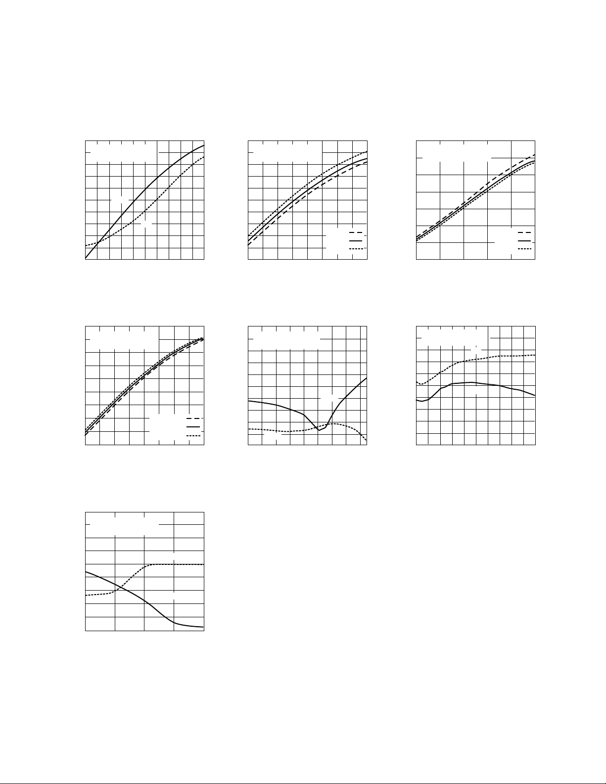
AT-31625 Typical Performance, T
= 25° C
C
Frequency = 900 MHz, VCE = 4.8 V, ICQ = 5 mA, CW operation, Test Circuit A, unless otherwise specified.
31
Γ
= 0.73 ∠ -156
source
29
Γ
= 0.42 ∠ -179
load
27
25
(dBm)
23
21
19
17
OUTPUT POWER
15
13
11
P
out
η
c
21412641081816 2220
INPUT POWER (dBm)
100
90
80
70
60
50
40
30
20
10
0
Figure 1. Output Power and Collector
Efficiency vs. Input Power.
32
Γ
= 0.73 ∠ -156
source
30
Γ
= 0.42 ∠ -179
(%)
COLLECTOR EFFICIENCY
load
28
26
(dBm)
24
22
20
18
OUTPUT POWER
16
14
12
INPUT POWER (dBm)
3.0 V
3.6 V
4.8 V
141261081816 2220
Figure 2. Output Power vs. Input
Power Over Bias Voltage.
100
Γ
= 0.73 ∠ -156
source
Γ
= 0.42 ∠ -179
load
90
(%)
80
70
60
50
40
COLLECTOR EFFICIENCY
30
12 1814 16 20 22
INPUT POWER (dBm)
Figure 3. Collector Efficiency vs.
Input Power Over Bias Voltage.
3.0 V
3.6 V
4.8 V
32
Γ
= 0.73 ∠ -156
source
30
Γ
= 0.42 ∠ -179
load
28
(dBm)
26
24
22
20
18
OUTPUT POWER
16
14
INPUT POWER (dBm)
TC = +85°C
= +25°C
T
C
= –40°C
T
C
141261081816 2220
Figure 4. Output Power vs. Input
Power Over Temperature.
0
Γ
= 0.73 ∠ -156
source
-2
Γ
= 0.42 ∠ -179
load
-4
-6
(dB)
-8
-10
-12
RETURN LOSS
-14
-16
-18
800 850 950 1000900
FREQUENCY (MHz)
Output R.L.
Input R.L.
Figure 7. Input and Output Return
Loss vs. Frequency.
0
Γ
= 0.73 ∠ -156
source
-5
Γ
= 0.42 ∠ -179
load
-10
-15
-20
(dBc)
-25
IMD
-30
-35
-40
-45
IMD
-50
81410 12 16 18 22 2420
Figure 5. IMD
Power Per Tone.
5
OUTPUT POWER/TONE (dBm)
, IMD5 vs. Output
3
IMD
31.0
Γ
30.5
Γ
30.0
29.5
(dBm)
29.0
28.5
3
28.0
27.5
OUTPUT POWER
27.0
26.5
26.0
800 920840 880 960 1000
Pin = +19 dBm
= 0.73 ∠ -156
source
= 0.42 ∠ -179
load
FREQUENCY (MHz)
100
90
(%)
η
c
P
out
80
70
60
50
40
30
20
COLLECTOR EFFICIENCY
10
0
Figure 6. Output Power and Collector
Efficiency vs. Frequency.
Note: Tuned at 900 MHz, then Swept over
Frequency.
4-45
 Loading...