

Page 1

TM 11-6625-2809-14 & P
TECHNICAL MANUAL
OPERATOR’S, ORGANIZATIONAL, DIRECT SUPPORT AND
GENERAL SUPPORT MAINTENANCE MANUAL
(INCLUDING REPAIR PARTS AND SPECIAL TOOLS LISTS)
FOR
MULTIMETER ME-498/U (HEWLETT-PACKARD
MODEL 34702A) (NSN 6625-00-538-9794)
AND
INDICATOR ID-2101/U (HEWLETT-PACKARD
MODEL 34750A) (NSN 6625-00-538-9758)
HEADQUARTERS, DEPARTMENT OF THE ARMY
JUNE 1979
Page 2

TM 11-6625-2809-14 & P
This manual includes copyright material reproduced by permission of the HEWLETT-PACKARD Company.
TECHNICAL MANUAL HEADQUARTERS
DEPARTMENT OF THE ARMY
No.11-6625-2809-14 & P Washington, DC
OPERATOR’S, ORGANIZATIONAL, DIRECT SUPPORT AND
GENERAL SUPPORT MAINTENANCE MANUAL
(INCLUDING REPAIR PARTS AND SPECIAL TOOLS LISTS)
FOR
MULTIMETER ME-4981U (HEWLETT-PACKARD MODEL 34702A)
(NSN 6625-00-538-9794)
AND
INDICATOR ID-21011U (HEWLETT-PACKARD MODEL 34750A)
(NSN 6625-00-538-9758)
REPORTING OF ERRORS
You can improve this manual by recommending improvements using DA
Form 2028-2 located in the back of the manual. Simply tear out the self-addressed
form, fill it out as shown on the sample, fold it where shown, and drop it in the mail.
If there are no blank DA Forms 2028-2 in the back of your manual, use the
standard DA Form 2028 (Recommended Changes to Publications and Blank
Forms) and forward to Commander, US Army Communications and Electronics
Materiel Readiness Command, ATTN: DRSEL-ME-MQ, Fort Monmouth, NJ 07703.
14June1979
In either case a reply will be forwarded direct to you.
This manual is an authentication of the m anufacturer’s commercial literature which, through usage, has been found to
cover the data required to operate and maintain this equipm ent. Since the manual was not prepared In accor dance with
military specifications and AR 310-3, the format has not been structured to consider levels of maintenance.
i
Page 3

Table of Contents TM 11-6625-2809-14 & P
TABLE OF CONTENTS
PART ONE
Section Page
0. INTRODUCTION........................................0-1
I. GENERAL INFORMATION........................1-1
1-1. Description....................................1-1
1-6. Specifications................................1-3
1-8. Options..........................................1-3
1-10. Accessories Available
(See Figure 1-2)............................1-3
1-11. Instrument and Manual
Identification .................................1-3
Section Page
II. INSTALLATION..........................................2-1
2-1. Introduction ...................................2-1
2-3. Initial Inspection.............................2-1
2-5. Power Requirements ....................2-1
2-7. Grounding Requirements .……….2-2
2-10. Environmental Requirements .……2-2
2-12. Instrument Mounting .....................2-2
2-13. Bench Use .…………....................2-2
2-15. Rack Use ......................................2-2
2-17. Repackaging for Shipment .…......2-2
2-21. Power Cords and Receptacles .….2-3
Section Page
III. OPERATING INSTRUCTIONS..................3-1
3-1. Introduction....................................3-1
3-3. Rear Panel Features.....................3-1
3-5. Warm-Up.......................................3-1
3-7. Operation with Plug-On Modules..3-1
Section Page
IV. THEORY OF OPERATION...........4-1
4-1. Introduction.................................................4-1
4-3. Basic Measurement Sequence..................4-1
4-5. Analog Circuits...........................................4-1
4-4. Input Amplifier............................................4-1
4-8. Integrator....................................................4-2
4-10. Zero Detect Circuits....................................4-2
4-12. Auto-Zero Cycle..........................................4-2
4-14. Digital Processing Circuits..........................4-2
4-17. Data Clock (Refer to
Figure 4-8)..................................................4-4
4-19. Timing Generator Circuit (See
Figure 7-8)..................................................4-4
4-21. Zero Detect and Data Transfer
(Refer to Figure 4-10).................................4-4
4-23. Data Accumulator and Storage
(Refer to Figure 7-7)...................................4-6
Section Page
4-25. Data Display and Control Circuits
(Refer to Figure 4-11) .…….......................4-6
4-27. Reset Timing (See Figure 4-12) ................4-7
4-29. Least Significant Digit Blank
(Refer to Figure 7-8) .…….........................4-7
Section Page
V. MAINTENANCE ........................................5-1
5-1. Introduction ...............................................5-1
5-3. Operational Checks ..................................5-1
5-6. Adjustment Procedures..............................5-1
5-8. Cover Removal..........................................5-2
5-10. Adjustment Locator ...................................5-2
5-12. Power Supply Adjustment .…....................5-2
5-13. Input Amp. Offset Adjustment ……............5-2
5-14. Zero Detect Comparator Offset ….............5-2
5-15. Zero Detect Hysteresis
Adjustment .………….................................5-2
5-16. Reference Voltage Adjustments …............5-3
Section Page
VI. IDENTIFICATION OF PARTS ..................6-1
6-1. Introduction .…………................................6-1
6-4. Deleted
6-6. Deleted
6-8. Proprietary Parts .…………….....................6-1
Section Page
VII. CIRCUIT DIAGRAMS AND
TROUBLESHOOTING .………..................7-1
7-1. Introduction .…………................................7-1
7-3. Troubleshooting .………............................7-1
7-4. Troubleshooting Trees .……......................7-1
7-6. Troubleshooting Procedures .....................7-1
7-8. Functional Block Diagram
(Figure 7-4) .………...................................7-1
7-10. Timing Circuits (Figure 7-5) ......................7-1
7-12. Schematic Diagrams (Figures
7-6, 7-7 and 7-8) .……...............................7-1
7-14. Component Location Diagrams ................7-1
APPENDIXES
A. Difference Data Sheet ...............................A-1
B. References ................................................B-1
C. Maintenance Allocation .…………………..C-1
D. Repair Parts And Special
Tools List...................................................D-1
ii
Page 4

Table of Contents TM 11-6625-2809-14 & P
LIST OF TABLES
Table Page
1-1. Specifications................................................ 1-2
1-2. General Information ...................................... 1-3
3-1. 34721B/5055A Output Codes....................... 3-1
5-1. Recommended Test Equipment ................... 5-1
5-2. DC Accuracy ................................................. 5-2
5-3(a). AC Accuracy (45 Hz and 20 kHz................... 5-5
5-3(b). AC Accuracy (100 kHz).................................5-6
5-4. Accuracy Test .............................................. 5-7
6-1. Identification of Parts..................................... 6-3
LIST OF ILLUSTRATIONS
Figure Page
1-1 Instrument Serial Number............................1-1
2-1. Installation of the Model 34702A..................2-1
3-1. Front add Rear Panel Features....................3-0
4-1. Block Diagram..............................................4-0
4-2. ACV/DCV Attenuator....................................4-1
4-3. W Converter.................................................4-2
4-4. AC/DC Converter......................................... 4-3
4-5. Impedance Converter...................................4-4
5-1. Input Impedance Test ..................................5-3
5-2. Effective Common Mode Rejection..............5-3
5-3. Normal Mode Rejection................................5-4
5-4. Removal from Case .....................................5-8
5-5. Adjustment Locator...................................... 5-9
7-1. AC Converter Troubleshooting Tree............7-3/7-4
7-2. W Converter Troubleshooting Tree..............7-3/7-4
7-3. 34702A Schematic.......................................7-5/7-6
iii
Page 5

TABLE OF CONTENTS
PART TWO
TM 11-6625-2809-14 & P
Section Page
I. GENERAL INFORMATION........................1-1
1-1. Description....................................1-1
1-6.Specifications.......................................1-3
1-8. Options..........................................1-3
1-10. Accessories Available
(See Figure 1-2) ...........................1-3
1-11. Instrument and Manual
Identification .……….....................1-3
Section Page
II. INSTALLATION .........................................2-1
2-1. Introduction....................................2-1
2-3. Initial Inspection.............................2-1
2-5. Power Requirements.....................2-1
2-7. Grounding Requirements..............2-2
2-10. Environmental Requirements........2-2
2-12. Instrument Mounting......................2-2
2-13. Bench Use.....................................2-2
2-15. Rack Use.......................................2-2
2-17. Repackaging for Shipment............2-2
2-21. Power Cords and Receptacles......2-3
Section Page
III. OPERATING INSTRUCTIONS..................3-1
3-1. Introduction....................................3-1
3-3. Rear Panel Features.....................3-1
3-5. Warm-Up.......................................3-1
3-7. Operation with Plug-On Modules .3-1
Section Page
IV. THEORY OF OPERATION........................4-1
4-1. Introduction....................................4-1
4-3. Basic Measurement Sequence ....4-1
4-5. Analog Circuits..............................4-1
4-6. Input Amplifier...............................4-1
4-8. Integrator.......................................4-2
4-10. Zero Detect Circuits.......................4-2
4-12. Auto-Zero Cycle.............................4-2
4-14. Digital Processing Circuits.............4-2
4-17. Data Clock (Refer to
Figure 4-8).....................................4-4
4-19. Timing Generator Circuit (See
Figure 7-8).....................................4-4
4-21. Zero Detect and Data Transfer
Circuits (Refer to Figure 4-10).......4-4
4-23. Data Accumulator and Storage
(Refer to Figure 7-7)......................4-6
Section Page
4-25. Data Display and Control Circuits
(Refer to Figure 4-11)...................4-6
4-27. Reset Timing (See Figure4-12)..................4-7
4-29. Least Significant Digit Blank
(Refer to Figure 7-7)..................................4-7
Section Page
V. MAINTENANCE.........................................5-1
5-1. Introduction................................................5-1
5-3. Operational Checks ..................................5-1
5-6. Adjustment Procedures..............................5-1
5-8. Cover Removal .........................................5-2
5-10. Adjustment Locator....................................5-2
5-12. Power Supply Adjustment..........................5-2
5-13. Input Amp. Offset Adjustment ...................5-2
5-14. Zero Detect Comparator Offset ................5-2
5-15. Zero Detect Hysteresis
Adjustment.................................................5-2
5-16. Reference Voltage Adjustments ...............5-3
Section Page
VI. IDENTIFICATION OF PARTS...................6-1
6-1. Introduction................................................6-1
6-4. Deleted
6-6. Deleted
6-8. Parts Changes...........................................6-1
6-10. Proprietary Parts
Section Page
VII. CIRCUIT DIAGRAMS AND
TROUBLESHOOTING...............................7-1
7-1. Introduction................................................7-1
7-3. Troubleshooting.........................................7-1
7-4. Troubleshooting Trees...............................7-1
7-6. Troubleshooting Procedures......................7-1
7-8. Functional Block Diagram
(Figure 7-4)................................................7-1
7-10. Timing Circuits (Figure 7-5).......................7-1
7-12. Schematic Diagrams (Figures
7-6, 7-7 and 7-8)........................................7-1
7-14. Component Location Diagrams.................7-1
Appendix Page
................................6-1
A. Difference Data Sheet.................................A-1
iv
Page 6

Table of Contents
TM 11-6625-2809-14 & P
LIST OF ILLUSTRATIONS
Figure Page
1-1. Plug-On Modules which can be used
with the 34750A Display Module................1-1
1-2. Accessories Available for use with 34750A.. 1-2
1-3. Instrument Serial Number (on rear panel) .1-3
2-1. Voltage Selection........................................2-1
2-2. Rick Mount Kits..........................................2-2
2-3. Power Receptacles....................................2-3
3-1. 34750A Rear Panel....................................3-1
4-1. Basic Block Diagram of 34750A.................4-0
4-2. Simplified Diagram of the
Input Amplifier............................................4-1
4-3. Simplified Diagram of the
Integrator Circuit.........................................4-2
4-4. Simplified Diagram of Zero Detect
Circuits......................................................4-2
4-5. 34750A Circuits shown in Auto-Zero
Mode ......................................................4-3
4-6. Block Diagram of Typical ASM...................4-3
4-7. ASM Simplified Block Diagram...................4-4
4-8. Data Clock..................................................4-4
Figure Page
4-9. 34750A Flow Chart....................................4-5
4-10. Zero Detect and Data Transfer
Timing......................................................4-6
4-11. Data Display Circuits..................................4-6
4-12. Reset Tuning .............................................4-7
5-I. 11456A Readout Test Card.......................5-1
5-2. Cover Removal..........................................5-2
5-3. Zero Detect Comparator Offset
Adjustment.................................................5-2
5-4. Chassis Mounted Component and
Adjustment Locator....................................5-3
7-1. Power Supply Troubleshooting
Tree ................................................7-3/7-4
7-2. Analog Troubleshooting Tree.....................7-5
7-3. Digital Troubleshooting Tree................7-7/7-8
7-4. Functional Block Diagram..................7-9/7-10
7-5. Timing Waveforms...........................7-11/7-12
7-6. Analog Signal Processor..................7-13/7-14
7-7. Digital Signal Processor...................7-15/7-16
7-8. Power Supply...................................7-17/7-18
LIST OF TABLES
Table Page
1-1. 3470A Series Signal Conditioning
Modules.........................................................1-3
1-2. Available Options..............................................1-3
5-1. Recommended Test Equipment.......................5-1
5-2. Operational Checks..........................................5-1
6-1. Identification of Parts........................................6-2
7-1. Troubleshooting Trees......................................7-1
v
Page 7

hp
PART ONE
OPERATING AND SERVICE MANUAL
Binder part No. 34740-90011
(Includes cover sheet)
Manual Part No. 34740-90012 or 34750-90012
(Binder, System Introduction and Display Manual)
MODEL 3470
MEASUREMENT SYSTEM
TM 11-6625-2809-14 & P
IMPORTANT NOTICE
This instruction manual requires no change sheet. Any
change information has already been integrated into the
manual by page revisions. Revised pages have a
revision letter which can be found on the lower corner
of the page. Reference may also be made to Section VIII
of each manual where backdating information for earlier
instruments can be found.
Copyright Hewlett-Packard Company 1972
P.O. Box 301, Loveland, Colorado 80537 U.S.A.
vi
Printed: June 1973
Page 8

TM 11-6625-2809-14 & P
hp
HEWLETT PACKARD
CERTIFICATION
Hewlett-Packard Company certifies that this instrument met its published specifications at the time of
shipment from the factory. Hewlett-Packard Company fur ther certifies that its calibration meas urements
are traceable to the United States National Bureau of Standards, to the ex tent allowed by the Bureau’s
calibration facility, and to the calibration facilities of other International Standards Organization members.
WARRANTY AND ASSISTANCE
This Hewlett-Packard produc t is warranted against defects in materials and work manship f or a period of
one year from the date of shipment, except that in the case of certain components, if any, listed in
Section I of this operating manual, the warranty shall be for the specif ied period. Hewlett-Pack ard will, at
its option, repair or replace products which prove to be defective dur ing the warranty period provided they
are returned to Hewlett-Packard, and provided the proper preventive maintenance procedures as listed in
this manual are followed. Repairs necessitated by misuse of the product are not covered by this
warranty. NO OTHER WARRANTIES ARE EXPRESSED OR IMPLIED, INCLUDING BUT NOT
LIMITED TO THE IMPLIED WARRANTIES OF MERCHANTABILITY AND FITNESS FOR A
PARTICULAR PURPOSE. HEWLETT-PACKARD IS NOT LIABLE FOR CONSEQUENTIAL DAMAGES.
If this product is sold as part of a Hewlett-Packard integrated instrument system, the above warranty shall
not be applicable, and this product shall be covered only by the system warranty.
Service contracts or customer assistance agreements are available for Hewlett-Packard products.
For any assistance, contact your nearest Hewlett-Packard Sales and Service Office, Addresses are
provided at the back of this manual.
vii
Page 9

INTRODUCTION
TM 11-6625-2809-14 & P
The 3470 Measurement System is a series of modules
that may be plugged together to form several different
measuring instrum ents, including both line powered and
battery powered versions.
A mainframe display module is connected to a bottom
plug-on function module to form a complete instrument.
The BCD and/or Battery plug-on module m ay be added
between the display and function modules as desired.
Refer to the Operating and Service Manual of the plugon module to be used with the display module for the
operating instructions, incoming inspection, and adjustment procedures of the instrument as a whole.
Possible Instrument Configurations
viii
Page 10

INTRODUCTION
0-1. SCOPE.
a. This manual in Part 1, describes
Multimeter ME-498/U (fig. 3-1) and provides instructions
for operation and maintenance. Throughout this manual
the ME-498/U is referred to as the Hewlett-Packard
Model 34702A.
SECTION 0
TM 11-6625-2809-14 & P
Improvement Report) as prescribed in AR
70058/NAVSUPINST 4030.29/AFR 71-13/MCOP40
30.29A and DLAR 4145.8.
c.
Discrepancy in Shipment Report
(DISREP) (SF 361). Fill out and forward Discrepancy in
Shipment Report (DISREP) (SF 361) as prescribed in
AR 55-38/NAVSUPINST 4610.33B/AFR 7518/MCO
P4610.19C and DLAR 4500.15.
b. Part 2 describes Indicator ID-2101/U
(fig.1-1, Part 2). This display module is referred to as the
Hewlett-Packard Model 34750A.
0-2. INDEXES OF PUBLICATIONS.
a.
of DA Pam 310-4 to determine whether there are new
editions, changes, or additional publications pertaining to
the equipment.
b.
to determine whether there are modification work orders
(MWO’s) pertaining to the equipment.
0-3. FORMS AND RECORDS.
a.
DA Pam 310-4.
DA Pam 310-7.
Reports of Maintenance and
Unsatisfactory Equipment.
and reports which are to be used by maintenance
personnel at all maintenance levels are listed in and
prescribed by TM 38-750.
b.
Deficiencies.
Report of Packaging and Handling
Fill out and forward DD Form 6 (Pac kaging
Refer to the latest issue
Refer to DA Pam 310-7
Maintenance forms, records,
0-4. REPORTING EQUIPMENT
IMPROVEMENT RECOMMENDATIONS (EIR).
EIR’s will be prepared using SF 368 (Quality Deficiency
Report). Instructions for preparing EIR’s are provided in
TM 38-750, the Army Maintenance Management
System. EIR’s should be mailed direct to Commander,
US Army Communication and Electronics Materiel
Readiness Command, ATTN: DRSEL-ME-MQ, Fort
Monmouth, NJ A reply will be furnished direct to you.
0-5. ADMINISTRATIVE STORAGE.
Administrative storage of equipm ent issued to and used
by Army activities shall be in accordance with TM 74090-1 and paragraph 2-8.
0-6. DESTRUCTION OF ARMY ELECTRONICS
MATERIEL.
Destruction of Army electronics materiel to prevent
enemy use shall be in accordance with TM 750-244-2.
0-1
Page 11

Model 34702A TM 11-6625-2809-14 & P
SECTION I
GENERAL INFORMATION
1-6. Table 1-1 lists specifications for the Model
1-1. INTRODUCTION.
34702A Multimeter. This table supersedes all other
previously printed specifications. Procedures are
1-2. This manual contains installation and operating
instructions as well as maintenance information which
includes performanc e checks for the Model 34702A. A
schematic diagram, theory of operation, and
troubleshooting information are provided for use in
maintaining the 34702A Multimeter Module.
provided in Section V to verify performance of the
instrument to its specifications and to readjust the
instrument if required. T he accuracy specifications apply
for ambient temperatures of 23
0
C+ 50C. For
temperatures outside this range, a temperature
coefficient factor (listed in Table 1-1) must be used.
1-3. DESCRIPTION.
1-4. The Hewlett-Packard Model 34702A Multimeter
is a signal conditioning module that m ay be connected to
a Model 34740A or 34750A Display Module, to measur e
AC Voltage, DC Voltage, or resistance. The AC and DC
volts functions provide four decade ranges from I V to
1000 V. Six resistance ranges from 100 full sc ale to 10
MQ full scale are provided by the "Ω (fy)" function. Each
available range of the Model 34702A has 100%
overranging capability except the 1000 V range which
has 20%.
Overload protection circuits allow up to
1200 V peak to be applied to the INPUT
V terminals without damaging the
instrument. Up to 350 V can be applied
to the INPUT S terminals without
damaging the instrument. No more than
500 V should be applied between LO
and Chassis. Do not apply voltage
between LO and Chassis when using
the 34721A or 34721B BCD Module.
These modules connect LO to Chassis
when attached to the Model 34 702A.
1-7. Table 1-2 lists general information relating to the
instrument.
1-8. INSTRUMENT AND MANUAL
IDENTIFICATION.
1-9. A three-section serial number (xxxxAxxxxx) is
used to identify your Model 34702A. Figure 1-1
illustrates the meaning of the three parts of the number.
1-10. This manual is kept up-to-date with revised
pages. If the serial number of your instrument is lower
than the one on the title page of this manual, refer to the
backdating inform ation in Appendix A which adapts this
manual to your instrument. All correspondence with
Hewlett-Packard Company should include the complete
serial number.
1-5. SPECIFICATIONS AND GENERAL
INFORMATION.
Figure 1-1. Instrument Serial Number.
1-1
Page 12

Model 34702A TM 11-6625-2809-14 & P
Table 1-1. Specifications. (Measured using 34740A or 34750A Display Unit)
DC VOLTAGE
34740A
Performance:
Accuracy (+ 230C t 50C), < 95% RH)
30 days + (0.03% of reading + .01% of range)
90 days + (0.04% of reading + .01% of range)
6 mo. + (0.05% of reading + .02% of range)
1 yr. + (0.06% of reading + .02% of range)
Stability (24 hours, + 230C + 1°C)
+ (0.01% of reading + 0.005% of range)
Temperature Coefficient (00 C to + 500C)
DC voltage: t (0.0035% of reading + 0.001%
of range)/oC.
Input Characteristics:
Input resistance
1 and 10 V ranges: 11.11 M + 0.2%
100 V range: 10.1 M + 0.2%
1000 V range: 10 M + 02%
Effective Common Mode Rejection (1 k unbalance)
DC: > 80 dB.*
Input impedance
1 and 10 V ranges: 11.11 M + 02%/ /80 pF max.
100 V range: 10.1 M ± 0.2%/ /80 pF max.
1000 V range: 10 M + 0.2%/180 pF max.
OHMS
34740A
Performance:
Accuracy (+ 230C ± 50C,< 95% RH)
30 days
10 MO range + (0.25% of reading + 0.02%
of range)
All other ranges + (0.05% of reading + 0.02%
of range)
90 days
10 M range + (0.30% of reading + 0.02%
of range)
All other ranges + (0.06% of reading + 0.02%
of range)
6 mo.
10 M range + (0.35% of reading + 0.03%
of range)
All other ranges + (0.07% of reading + 0.03%
of range)
Normal Mode Rejection
50 Hz (Option 050): >60dB (50 Hz + 0.1%)
60 Hz (Option 060): >60dB (60 Hz + 0.1%)
*Does not apply when BCD Module is used.
AC VOLTAGE
34740A
Performance:
Accuracy (+ 23°C + 50C, <95% RH)
30 days
45 Hz to 20 kHz + (0.25% of reading + .05%
of range)
20 kHz to 100 kHz + (0 75% of reading + .05%
of range)
90 days
45 Hz to 20 kHz + (0.30% of reading + .05%
of range)
20 kHz to 100 kHz + (0.80% of reading + .05%
of range)
6mo.
45 Hz to 20 kHz + (0.35% of reading + .05%
of range)
20 kHz to 100 kHz + (085% of reading + .05%
of range)
1 yr.
45 Hz to 20 kHz + (0.50% of reading + 0.05%
of range)
20 kHz to 100 kHz + (1.0% of reading + 0.05%
of range)
Temperature Coefficient (0°C to + 500C)
AC voltage: ± (0,03% of reading + 0.001%
of range) /0C.
Stability (24 hours, + 23°C + 1°C)
AC voltage: 45 Hz to 20 kHz: ± (0.15% of reading
+ 0.05% of range)
20 kHz to 100 kHz: + (0.4% of reading
+ 0.05% of range)
Response Time: < 2 s within + 0.3% of final value or 20
counts, whichever is greater.
Input Characteristics:
1 yr.
10 M range ± (0.50% of reading + 0.03%
of range)
All other ranges t (0.11% of reading + 0.03%
of range)
Stability (24 hours, 23°C + 10C)
10 Mn range + (0.1% of reading + 0.01%
of range)
All other ranges + (0.02% of reading + 0.02%
of range)
Temperature Coefficient (00C to + 500C)
Ω
10 Ml range: + (0.035% of reading + 0.001%
of range) / C.
All other ranges' t (0.006% of reading + 0.001%
of range) / C.
DC VOLTAGE
34750A
Performance:
Accuracy (+ 23°C + 50C), < 95% RH)
30 days ± (0.025% of reading + .005% of range)
90 days + (0.035% of reading + .005% of range)
6 mo. + (0.045% of reading + .007% of range)
1 yr. + (0.06% of reading + .01% of range)
NOTE: Due to temperature change inside the instrument
between line and battery operation, the references
must be adjusted when changing modes to achieve
these specifications
Stability (24 hours, + 230C + 10C)
DC voltage: + (.008% of reading i .004% of range)
Temperature Coefficient (0°C to + 500C)
DC voltage: ± (0.0025% of reading + 0.0002% of
range) / C
Input Characteristics
Input resistance
1 and 10 V ranges: 11.11 M + 0.2%
100 V range: 10.1 M +.0.2%
1000 V range: 10 M + 0.2%
Effective Common Mode Rejection (1 kO unbalance)
DC: >80 dB.*
*Does not apply when BCD Module is used
Rev. A 1-2
Page 13

Model 34702A TM 11-6625-2809-14 & P
Table 1-1. Specifications (Cont’d).
Normal Mode Rejection
50 Hz (Option 050): >60 dB (50 Hz + 0.1%)
60 Hz (Option 060): >60 dB (60 Hz + 0.1%)
AC VOLTAGE
34750A
Performance:
Accuracy (+ 230 + 5C, A 95% RH)
30 days
45 Hz to 20 kHz +(0.25% of reading + .05%
of range)
20 kHz to 100 kHz + (.75% of reading + .05%
of range)
90 days
45 Hz to 20 kHz + (.3% of reading + .05%
of range)
20 kHz to 100 kHz + (.8% of reading + .05%
of range)
6 mo.
45 Hz to 20 kHz ± (.35% of reading + .05%
of range)
20 kHz to 100 kHz + (.85% of reading + .05%
of range)
1 yr.
45 Hz to 20 kHz + (0.50% of reading + 0.05%
of range)
20 kHz to 100 kHz ± (1.0% of reading + 0.05%
of range)
Stability (24 hours, + 230C ± 10 C)
AC voltage: 45 Hz to 20 kHz: + (0.15% of reading
+ 0.05% of range)
20 kHz to 100 kHz: + (0.4% of reading
+ 0.05% of range)
Temperature Coefficient (0oC to + 50°C)
AC voltage: + (0.03% of reading + 0.001%
of range) /°C
Response Time: < 2 s within + 0.3% of final value or 200
counts, whichever is greater.
Input Characteristics:
Input impedance
1 and 10 V ranges: 11.11 M + 0.2%/1 /80 pF max.
100 V range: 10.1 M + 0.2%1/80 pF max.
1000 V range: 10 M + 0.2%/ /80 pF max.
OHMS
34750A
Performance:
Accuracy (+ 23oC + 5°C, < 95% RH)
30 days
10 M range ±(0.25% of reading + 0.015%
of range)
All other ranges + (0.045% of reading + 0.015%
of range)
90 days
10 M range ± (0.3% of reading + 0.015%
of range)
All other ranges + (0.055% of reading + 0.015%
of range)
6 mo.
10 M range ± (0.35% of reading + 0.02%
of range)
All other ranges + (0.065% of reading + 0.02%
of range)
1 yr
10 M range ± (0.50% of reading + 0.02%
of range)
All other ranges + (0.11% of reading + 0.02%
of range)
NOTE: Due to temperature change inside the instrument
between line and battery operation, the references
must be adjusted when changing modes to achieve
these specifications.
Stability (24 hours, 23°C ± 1oC)
10 M range + (0.1% of reading + 0.009% of range)
All other ranges + (0.2% of reading + 0.015% of range)
Temperature Coefficient (0o C to + 50o C)
10 M range: ± (0.035% of reading + 0.001%
of range) /°C
All other ranges: +(0.006% of reading + 0.001%
of range) /oC
DC VOLTAGE
34740A
Ranges:
Full Scale Maximum
Range Reading Reading
1 V ± 1.0000 V ± 1.9999 V
10 V ± 10.000 V ± 19.999 V
100 V ± 100.00 ±199.99 V
1000 V + 1.0000 V ±1200.0 V
Overrange
1000 V range: 20%.
All other ranges: 100% (19999 max reading)
Range Selection: manual pushbuttons
Performance:
Reading Rate
Option 050 (50 Hz): 8/s fixed
Option 060 (60 Hz): 5/s fixed
Table 1-2. General Information.
Input Characteristics:
Input terminals: floating pair.*
Maximum input voltage
High to low 1200 V
Low to Chassis + 500V*
*Does not apply when BCD Module is used.
AC VOLTAGE
34740A
Ranges:
Full Scale Maximum
Range Reading Reading
1 V 1.0000 V 1.9999 V
10 V 10.000 V 19.999 V
100 V 100.001 199.99 V
1000 V 1.0000 V 1200.0 V
Rev. A 1-3
Page 14

Model 34702A TM 11-6625-2809-14 & P
Table 1-2. General Information (Cont’d).
Overrange
1000 V range: 20%
All other ranges: 100% (19999 max reading)
Range selection- manual pushbuttons
Performance:
Frequency range: 45 Hz to 100 kHz
Input Characteristics:
input terminals: floating pair. *
Maximum input voltage
High to low: 1200 V rms. Except 1 V range.
1 V Range:
1200 V rms maximum 45 Hz - 200 Hz
300 V rms maximum 200 Hz - 100 kHz
Low to Chassis: + 500 V *
* Does not apply when BCD Module is used.
Ω
34740A
Ranges:
Range
100 Ω
1 κΩ
10 κΩ
100 κΩ
1000 κΩ
10 ΜΩ
Full Scale
Reading
100.00 Ω
1.0000 ΚΩ
10.000 ΚΩ
100.00 ΚΩ
1000.0 ΚΩ
10.000 ΜΩ
Maximum
Reading
199.99 Ω
1.9999 ΚΩ
19.999 ΚΩ
199.99 ΚΩ
1999.9 ΚΩ
19.999 ΜΩ
Overrange
1000V range: 20%
All other ranges 100% (199999 max reading)
Range selection: manual pushbuttons
Reading rate
Option 050 (50 Hz): 4/s fixed
Option 060 (60 Hz). 5/s fixed
Input terminals: floating pair *
Maximum Input voltage
High to Low: + 1200 V
Low to Chassis: + 500 V·*
* Does not apply when BCD Module is used.
AC VOLTAGE
34750A
Ranges:
Range
1 V
10 V
100 V
1000 V
Overrange
1000 V range: 20%
All other ranges. 100% (199999 max reading)
Range selection: manual pushbuttons
Full Scale
Reading
1.00000 V
10.0000 V
100.000 V
1000.00 V
Maximum
Reading
1.99999 V
19.9999 V
199.999 V
1200.00 V
Overrange: 100% on all ranges
Range selection: manual pushbuttons
Input Characteristics:
Input terminals: floating pair (different from voltage
input terminals).
Current through measured resistor: 10 mA on 100 Ω
range decreasing one decade per successively higher range.
Effective Common Mode Rejection: same as dc spec-
ifications.
Overload protection: + 350 V peak (248 V rms sine
wave).
Other:
Operating temperature: 0°C to + 50°C.
Storage temperature: - 40oC to + 75oC.
Line requirements: 100/120/220/240 V
- 10%, + 5% switchable:
DC VOLTAGE
34750A
48 Hz to 440 Hz; < 8.7 VA.
Ranges:
Range
1 V
10 V
100 V
!000 V
Full Scale
Reading
+ 1.00000 V
+ 10.0000 V
+ 100.000 V
+ 1000.00 V
Maximum
Reading
+ 1.99999 V
+ 19.9999 V
+ 199.999 V
+ 1200.00 V
Frequency range: 45 Hz to 100 kHz
Input terminals: floating pair
Maximum input voltage
High to Low: 1200 V rms except on 1 V range.
On 1 V range 2.5 x 10⁵ V Hz limit with minimum protection of 300 V rms.
Low Chassis: + 500 V
Ω
34750A
Ranges:
100 Ω 100.000 Ω 199.99 Ω
1 κΩ 1.00000 κΩ 1.99999 κΩ
10 κΩ 10.0000 κΩ 19.9999 κΩ
100 κΩ 100.000 κΩ 199.999 κΩ
1000 κΩ 1000.00 κΩ 1999.99 κΩ
10 ΜΩ 10.0000 ΜΩ 19.9999 ΜΩ
Overrange: 100% on all ranges
Range: selection manual pushbuttons
Input terminals: floating pair (different from voltage
input terminals).
Current through measured resistor: 10 mA on 100 Ω
range decreasing one decade per successively higher range.
Effective Common Mode Rejection: same as dc spec-
ifications.
Overload protection- t 350 V peak (248 V rms sine
wave).
Rev. A 1-4
Page 15

Model 34702A TM 11-6625-2809-14 & P
SECTION II
INSTALLATION
2-1. INTRODUCTION.
2-2. This section contains installation and shipping
information for the Model 34702A.
2-3. INITIAL INSPECTION.
2-4. The Model 34702A should be inspected upon
receipt for damage that might have occurr ed in transit. If
there is damage due to shipping, file a claim with the
carrier. If there are other electrical or mechanical
deficiencies refer to the warranty statement on the back
of the title page. Use the procedures pr ovided in Sec tion
V to check instrument performance.
2-5. CONNECTION TO THE DISPLAY MODULE.
2-6. Referring to Figure 2-1, connect the Model
34702A to the Display Module using the following
procedure:
a. Pull the side locks on the Display Module to the
rear.
b. Pos ition the Display Module and 34702A together
so that the tabs and slots on the sides of the two units
interlock.
c. Push the side locks toward the Display Module.
This pulls the two units together and locks them.
2-7. If a 34720A Battery Module or a 34721B BCD
Module is to be used between the display module and
the 34702A then the side locks on this middle module
hold the 34702A.
2-8. REPACKAGING FOR SHIPMENT.
2-9. If the instrument is to be shipped to HewlettPackard for service or repair, attach a tag to the
instrument describing the work to be accomplished and
identifying the owner of the instrument. Identify the
instrument by serial number, m odel num ber and nam e in
any correspondence. If you have any questions, contact
your local Hewlett-Packard Sales and Service Office.
2-10. If the original shipping container is to be used,
place the instrument in the container with appropriate
packing material and seal the container well with strong
tape or metal bands.
2-11. If an -hp- container is not to be used, use a
heavy carton or wooden box with an inner container.
Wrap the instrument with heavy paper or plastic and
place cardboard strips across the face for protection
before placing the instrument in the inner container. Us e
packing material around all sides of the inner container,
and seal the outer container well with strong tape or
metal bands. Mark the container with "DELICATE
INSTRUMENT" or "FRAGILE."
Figure 2-1. Installation of the Model 34702A
2-1
Page 16

Model 34702A TM 11-6625-2809-14 & P
Figure 3-1. Front and Rear Panel Features.
3-0
Page 17

Model 34702A TM 11-6625-2809-14 & P
SECTION III
OPERATING INSTRUCTIONS
3-1. INTRODUCTION.
3-2. This section contains instructions and info rmation
which will assist you in proper operation of the Model
34702A Multimeter Module. A Model 34740A or 34750A
Display Module is required to operate the Model 34702A.
Included in this section is identification of controls,
indicators and connectors; operating procedures; and
BCD output code information (for use in conjunc tion with
the 34721B BCD Module).
3-3. PANEL FEATURES.
3-4. The panel features of the instrument are
described in Figure 3-1.
3-5. FRONT PANEL OPERATION.
3-6. There are two manual controls; the function
switch and the range switch (See Figure 3-1). Each
range, except the 1000V range, has 100% overranging
capability; e.g. using a four digit display module 1.9999 V
can be measured on the I V range. T he display blanks
at 200% of range, indicating an overload.
Overload protection circuits allow up to
1200 V peak to be applied to the
INPUT V terminals without damaging
the instrument. Up to 350 V can be
applied to the INPUT Ω.
terminals without damaging the instrument. No
more than 500 V should be applied between LO
and Chassis (Grnd. ). Do not apply voltage
between LO and Chassis when using the 34721A or
34721B BCD Module. These modules connect LO
to Chassis when attached to the Model 34702A.
3-7. DC Voltage Measurement.
3-8. Set the Function switch to DCV, select the
required voltage range, and apply the voltage to be
measured to the INPUT V terminals.
3-9. AC Voltage Measurement.
3-10. Set the function switch to ACV, select the
required voltage range, and apply the voltage to be
measured to the INPUT V terminals.
3-11. Resistance Measurement.
3-12. Set the function switch to Ω (92), select the
required resistance range, and connect the device to be
measured to the INPUT Ω terminals.
3-13. 34721B/5055A OUTPUT CODES.
3-14. Output codes obtained from a 34721B BCD
Module when used in conjunction with the Model 34702A
and a display module are listed in Table 3-1. Refer to
the 34721B Operating and Service Manual for further
information regarding the BCD Module
.
Table 3-1. 34721B5055A Output Codes
Polarity
Number
Printed
0 DCV underrange O
1 + 10000 ACV overrange 1
2 1000 1000
3 100 100 3
41010 4
511 5
6.1.1 6
7 7
8 8
9 9
Overload
Column 9
Range
Column 8
Ω
k
Volts
Function
Column 7
Ω
k
3-1
Overrange
Column 6
Digits Columns
1 through 5
2
Page 18

Model 34702A TM 11-6625-2809-14 & P
Figure 4-1. Block Diagram.
4-0
Page 19

Model 34702A TM 11-6625-2809-14 & P
SECTION IV
THEORY OF OPERATION
4-1. INTRODUCTION.
4-2. This section contains a des cription of the Model
34702 Multimeter in simplified form followed by a more
detailed functional description. A detailed circuit
schematic is shown in Figure 7-3.
4-3. BLOCK DIAGRAM DESCRIPTION.
4-4. The circuits of the Model 34702A can be divided
into four major blocks shown in Figure 4-1.
4-5. ACV And DCV Attenuator.
4-6. The ACV/DCV Attenuator reduces the level of
the signal applied to the input so that it can be measur ed
by the 34740A or 34750A Display Module. The signal
can be attenuated by a factor of I, 10, 100 or 1000.
4-7. Current Source.
4-8. Resistance measurem ents are m ade by passing
a known current through the resistor being measured
and then measuring the voltage developed across the
resistor. The current source supplies five different
currents used by the six available ohmmeter ranges.
Resistance of an unknown is measured by connecting it
across the Ω terminals and selecting Ω function.
4-9-. Range/Function Switches
4-10. Range and Function switching is accomplished
by manual selection. Data from the Range and Function
switches is supplied to the Display Module, and to the
BCD Module when it is connected.
4-11. AC Converter.
4-12. The AC Converter accepts ac voltage from the
attenuator and changes it to a dc voltage proportional to
the level of the applied signal.
4-13. DETAILED THEORY OF OPERATION.
4-14 ACV/DCV Attenuator.
4-15. Figure 4-2 shows the ACV/DCV Attenuator with
its AC and DC voltage accuracy adjustments deleted.
Resistors R3, R5, and R7, shown in Figure 7.3 are dc
adjustments. Capacitors C3 through Cl 1, also shown in
Figure 7-j provide ac compensation for the attenuator.
4-16. Ω Converter.
4-17. Current Source. A simplified diagram of the
Ω
meter current source is shown in Figure 4-3a. Zener
diode CRI6 is the voltage reference for the current
source.
Figure 4-2. ACV/DCV Attenuator.
4-1
Page 20

Model 34702A TM 11-6625-2809-14 & P
Amplifier A is connected in a non-inverting configuration
and R
range) is developed across R
is adjusted such that 1 V (.1 V for the 10MIO
b
and R
a
Amplifier B has its
b.
+ input connected to a stable dc voltage of -6.2 V. T he input is connected to the output of Amplifier A through
the range reference resistors R52 - R56. The I V ac ross
and Rb causes the output of Amplifier B to become
R
a
more positive. This allows the current through Qx to vary
such that the - input of Amplifier B becomes
approximately -6.2 V. The input current to Am plifier B is
very small. Consequently the current that flows through
the range reference resistors is the s ame as the current
supplied by the source of Qx. The drain current of Qx is
almost identical to its source current because the gate
current is extremely small. The drain current flows
through Rx and develops a dc voltage which is applied to
the Display Module input. The output current, I
, is
x
changed for different resistance ranges by changing the
value of R
On the 10 M Ω range
a.
Switch Sb is in the 10 M Ω position which reduces the
voltage between points 4 and 5 to .1 V.
4-18. Ohms Protection Circuit. The actual circuit
represented by Qx in Figure 4-3a is shown in Figure 43b. The ohmmeter circuits are protected for voltages
applied to the "Ω (f’)" input up to 350 V peak. Large
negative voltages are blocked by CR12. Large positive
voltages are blocked by the high collector to base
breakdown voltages of Q13 and Q14. CR13 conducts
for positive voltages greater than approximately 2 V,
causing CR14 to conduct.
Figure 4-3. Ohms Converter.
4-2
Page 21

Model 34702A TM 11-6625-2809-14 & P
turning on Q12. This places - 12 V at the collector of
Q12 which turns off transistors QI 1, Q13, and Q14.
419. AC Measuring Circuits.
420. A simplified diagram of the circuits used to
measure ac voltage is shown in Figure 4-4.
The attenuation of the input signal by the Attenuator
for the four ac voltage ranges is:
Range Attenuation Factor
1V X 1
1OV X 0.1
100V X 0.01
1000V X 0.001
The output voltage of the attenuator is buffered by the
Impedance Converter. The voltage gain of the
Impedance Converter is adjustable and is appr oximately
one. Its input impedance is very high to minimize loading
of the Attenuator and its output resistance is low to drive
the Converter Amplifier. T he AC Converter yields a dc
output voltage that is proportional to the average value of
the negative half-wave rectified input signal. The
resulting voltage is filtered and m easured by the Display
Module.
4-21. Impedance Converter. A simplified diagram of
the Impedance Converter is shown in Figure 4-5. The
input transistor Q1 is a sourc e follower. Transistors Q2
and Q3 constitute an amplifier that provides bias c urrent
to Q1 and a high input resistance (load resistance) for
Q1. A positive going voltage at point 1 causes the
voltage at point 2 to increase. This incr eased voltage at
point 2 increases the
Figure 4-4. Ac/DC Converter.
4-3
Page 22

Model 34702A TM 11-6625-2809-14 & P
current through Q2. The increased current causes the
voltage at point 4 to increase. Since Q3 is an emitter
follower, point 3 will also increase and follow very closely
the voltage at point 2. Since the output voltage is taken
at the emitter of Q3, RI3 m ay be increased to make the
gain of the amplifier greater than unity.
4-22. AC Converter. Refer to Figure 4-4 for the
following discussion. Overall ac feedback is supplied
from point 5 back to the inverting input. The voltage at
point 5 is similar in shape to the voltage at point 2,
inverted and about one-half the amplitude. Current for
the negative half of the waveform at point 5 flows
through CR8, R31 and R33. Current for the positive half
of this waveform f lows through CR9, R32 and R33. The
output voltage is taken at the cathode of CR9, filtered by
the Low Pass Filter and measured by the Display
Module. The DC Feedback Amplifier provides a low
frequency feedback path around the Converter Amplifier
to keep the Converter Amplifier biased properly.
Figure 4-5. Impedance Converter.
4-4
Page 23

WARNING
These servicing instructions are for use by qualified personnel
only. To avoid electrical shock, do not perform any servicing
other than that contained in the operating instructions unless
you are qualified to do so.
5-0
TM 11-6625-2809-14 & P
Page 24

Model 34702A TM 11-6625-2809-14 & P
SECTION V.
MAINTENANCE
5-1. INTRODUCTION.
5-2. This section contains information necessary for
maintenance of the -hp- Model 34702A Multimeter.
Included are Performance Tests and Adjustment
Procedures for the 30 day, 90 day, 6 month, and I year
intervals referred to in Table 1-1. To determine the
optimum calibration interval for your instrument, refer to
MIL Specification MILC-45662A. If, after completing the
Performance Checks, you find that the instrument does
not meet its required specifications, refer to the
Adjustment Procedure (Paragraph 5-16). Attempt to
readjust the instrument to bring it into specification. If,
after adjusting the instrument, it is still out of
specification, refer to troubleshooting in Section VII.
5-3. RECOMMENDED TEST EQUIPMENT.
5-4. The test equipment that is recommended for
maintaining the Model 34702A is listed in Table 5-1. If
the recommended model is not available, use equipment
that has specifications equal to or better than those
listed.
5-5. PERFORMANCE TESTS.
5-6. The following tests verify that the Model 34702A
is operating properly and meets the specifications listed
in Table 1-1 of this manual. These tests should be
completed before any attempt is made to adjust the
instrument.
5-7. A Performance Test Record is provided at the
end of this section for recording the results of the
Performance Tests.
5-8. All of the following tests have been written to
include the use of either a 34740A or 34750A Display
Module.
Table 5-1. Recommended Test Equipment.
Instrument
Type
AC Calibrator 1 V, 10 V, 100 V
100 Ω, 1ΚΩ
10ΚΩ, 100ΚΩ
1ΜΩ, 10ΜΩ
standard resistors
DC Standard 1 V, 10 V, 100 V,
Electronic
Counter
Required
Characteristics
1000 V, 45 Hz to
100 kHz
Accuracy: +0.04%
of setting (45 Hz to
20 kHz)
+ 0.15% of setting
(100 kHz)
Accuracy: +0.01%
1000 V Ranges
Accuracy: +0.008%
Capable of measuring the period of
50 Hz or 60 Hz to
within + .01%
Recommended
-hp- Model
745A/746A
General Radio
Model GR 1433-Z
Decade Resistor
-hp- 740B
-hp- Model 5300A/
5302A
34750A
Accuracy (+ 23
o
C + 5oC), <95% RH):
30 days +(0.025% of reading + .005% of range)
90 days ±(0.035% of reading + .005% of range)
6 mo. ±(0.045% of reading + .007% of range)
1 yr. ±(0.06% of reading + .01% of range)
RECOMMENDED TEST EQUIPMENT:
DC Standard, -hp- Model 740B
TEST PROCEDURE:
Model
5-9. DC Accuracy Test (DCV Function).
DESCRIPTION:
This test verifies the ability of the Model 34702A to
measure dc voltage accurately within the specification
limits.
SPECIFICATION.
34740A
Accuracy (+ 23o C + 5o C), < 95% RH):
30 days + (0.03% of reading + .01% of range)
90 days + (0.04% of reading + .01% of range)
6 mo. + (0.05% of reading + .02% of range)
1 yr .+ (0.06% of reading + .02% of range)
a. Select the DCV function of the Model 34702A
and connect a dc standard (-hp- Model 740B or
equivalent) to the 34702A INPUT V terminals.
b. Check dc accuracy for both polarities of input
according to Table 5-2. Apply short to 34702A input to
check 0 V reading on all ranges.
NOTE
With 1000 V applied only the positive
polarity is checked due to the possibility
of arcing within the Model 740B.
Rev. B 5-1
Page 25
Model 34702A PERFORMANCE TEST TM 11-6625-2809-14 & P
Table 5-2. DC Accuracy.
5-10. Input Impedance Test (DCV and ACV
Function).
DESCRIPTION:
Input impedance affects the ability of a voltmeter to
accurately measure a given voltage because of loading
effects caus ed by the impedance Nor mally, it is desirable
to achieve as high an input impedance as pos sible. T his
check ensures that the input Impedance of the Model
34702A meets the specifications listed below.
SPECIFIC ATION:
Input Resistance
1 and 10 V ranges: 11.11 ΜΩ + 0.2% <
100 V range: 10.1 ΜΩ + 0.2% <80 pF
1000 V range: 10 ΜΩ ± 0.2% < 80 pF
RECOMMENDED TEST EQUIPMENT:
AC Calibrator, -hp- Model 745A
DC Standard, -hp- Model 740B
Resistance Decade, GR Model 1433-Z
TEST PROCEDURE:
a. Connect the equipment as shown ill Figure 5-1.
The Model 34702A should be set to DCV on the 1 V
range.
80 pF
Rev. B 5-2
b. Set the resistance decade to 10 ΜΩ and then
shunt it with a jumper lead. Set the DC standard for +
1.0000 V (34740A Display) or + 1.00000 V (34750A
Display) as observed on the Display Module.
c. Remove the jumper lead and again observe the
display. It should read between .5258V and .5268V
(34740A) or between .52582 and .52681 (34750A).
NOTE
The 34702A is not checked on the 10 V
range since the input circuit is equiv alent
for both the 1 V and the 10 V ranges.
d. Set the Model 34702A to the 100 V range and
short the resistance box with a jumper lead.
e. Set the dc standard for + 100.00 V (34740A) or
+ 100.000 V (34750A) as observed on the Display
Module.
WARNING
Use extreme cauti
on
when removing or
replacing the jumper in Steps f, g and i
to avoid electrical shock when
performing the input impedance test on
the 100 V’ and 1000 V ranges.
Page 26

Model 34702A PERFORMANCE TEST
Figure 5-1. Input Impedence Test.
f. Turn the dc standard OUTPUT to OFF.
Remove the jumper from the resistance box. Set dc
standard OUTPUT to ON and again observe the display.
It should read 50.20 to 50.30 (34740A) or 50.201 to
50.301 (34750A).
The 34702A display should indicate >.7059 (34740A) or>
.70594 (34750A). This verifies the 34702A input
capacity specification.
TM 11-6625-2809-14 & P
I. Change the ac standard fr equency to 20 kHz.
g. Turn the dc standard OUTPUT to OFF. Set
the Model 34702A to the 1000 V range and short the
resistance box with a jumper lead.
h. Turn the dc standard OUTPUT to ON. Set
the dc standard for + 1000.0 V (34740A) or + 1000.00
V (34750A) as observed on the Display Module.
i. Turn the dc standard OUTPUT to OFF.
Remove the jumper from the resistance box. Turn the
dc standard OUTPUT to ON and again observe the
display. It should read 499.7 to 500.7 (34740A) or
499.75 to 500.75 (34750A).
j. Set the dc standard OUTPUT to zero.
Replace dc standard with the ac standard.
k. Set the Model 34702A to the 1 V range.
Replace the resistance box with a 100 κΩ resistor (-hpPart Number 0757-0465). Connect one end of the
resistor directly to the HI terminal. Set the ac s tandard
frequency to I kHz. Adjust the ac standar d am plitude for
+ 1.0000 V i 1 count(34740A) or + 1.00000 V + 1 c ount
(34750A) as observed on the Display Module.
5-1. DC Effective Common Mode Rejection.
DESCRIPTION:
Effective Common Mode Rejection (ECMR) is a
measure of the eff ect of a com mon mode s ource on the
measured value or readout of the instrument with a
1kohm unbalance. Typically ECMR is measured in
decibels (dB) and can be calculated by the following
formula:
Common Mode Voltage Applied
ECMR (dB) = 20 log10 (
________________________________________
Change in Display Indication
SPECIFICATION
:
Effective Common Mode Rejection (I
κΩ
unbalance): > 80 dB.
RECOMMENDED TEST EQUIPMENT:
DC Standard, -hp- Model 740B
Resistor, I κΩ t 1% (resistance decade may be used for
this)
)
Figure 5-2. Effective Common Mode Rejection
Rev. C 5-3
Page 27

Model 34702A PERFORMANCE TEST TM 11-6625-2809-14 & P
TEST PROCEDURE
a. Disconnect all previous connections to the
Model 34702A input and connect the equipment as
-2.
shown in Figure 5
Set the dc standard for a +10 V
output. Set the 34702A to the I V range.
b. Observe the voltmeter display. It should read
less than 10 counts (34740A Display) or 100 counts
(34750A Display). This verifies an effective common
mode rejection at dc of > 80 dB.
5-12. Normal Mode Rejection.
DESCRIPTION:
Normal Mode Rejection (NMR) is a measure of the ability
of the Model 34702A to reject ac signals applied to the
INPUT V terminals while the instrument is operating in
DCV function. NMR is measured in decibels (dB) and
can be calculated by the following formula:
Peak Normal Mode Voltage
____________________________________
NMR (dB) = 20 log
(
10
)
Peak Display Indication
SPECIFICATION:
Normal Mode Rejection: Greater than 60 dB (at 50 Hz
t 0.1%or 60 Hz ± 0.1%).
RECOMMENDED TEST EQUIPMENT:
AC Calibrator, -hp- Model 745A
Electronic Counter, -hp- Model 5300A/5302A
TEST PROCEDURE:
a. Disconnect all previous connections to the
34702A input and connect the equipment as
shown in Figure 5-3. Set the Model 34702A to
DCV and the 1 V range.
b. Adjust the ac calibrator output for .707 V rms (1V
peak).
c. Set the counter controls to meas ure period and
adjust the ac calibrator frequenc y for a counter indic ation
between 16.650 ms and 16.683 ms (19.980 ms to
20.020 ms for Option 050). The Display Module should
read <10 counts (34740A Display) or <100 counts
(34750A Display).
5-13. AC Accuracy.
DESCRIPTION:
This test verifies the ability of the Model 34702A to
measure ac voltage accurately to within the specification
tolerances.
SPECIFICATION:
34740A
Accuracy (+ 23°C ± 5°C, <95% RH)'
30 days
45 Hz to 20 kHz +(0.25% of reading +
.05% of range)
5%
20 kHz to 100 kHz +(0.7
of reading +
.05% of range)
90 days
45 Hz to 20 kHz +(0.30°c of reading +
.05% of range)
20 kHz to 100 kHz +(0.80% of reading +
.
05% of range)
6 mo.
45 Hz to 20 kHz +(0.35% of reading +
.05% of range)
20 kHz to 100 kHz +(0.85% of reading +
.05% of range)
I yr.
45 Hz to 20 kHz +(0.50% of reading +
0.05% of range)
20 kHz to 100 kHz +(1.0% of reading +
0.05% of range)
Figure 5-3. Normal Mode Rejection.
Rev. A 5-4
Page 28

Model 34702A PERFORMANCE TEST TM 11-6625-2809-14 & P
34750A
Accuracy (+ 23
30 days
45 Hz to 20 kHz +(0.25% of reading +
20 kHz to 100 kHz +(.75% of reading +
90 days
45 Hz to 20 kHz ±(.3% of reading +
20 kHz to 100 kHz +(.8% of reading +
6 mo.
45 Hz to 20 kHz +(.35% of reading +
20 kHz to 100 kHz +(.85% of reading +
1 yr.
45 Hz to 20 kHz ±(0.50% of reading +
20 kHz to 100 kHz ±(1.0% of reading +
o
C + 5°C, < 95% RH):
.05% of range)
.05% of range)
.05% of range)
.05% of range)
.05% of range)
.05% of range)
0.05% of range)
0.05% of range)
AC Calibrator/High Voltage Amplifier, -hp- Model
745A/746A or equivalent.
TEST PROCEDURE:
a. Set the Model 34702A function switch to ACV
and select the I V range. Apply short to 34702A input
and check 0 V reading on all ranges.
b. Using an ac calibrator and a high voltage
amplifier (-hp- Model
745A/746A
recommended), check
the accuracy of the Model 34702A for inputs other than 0
V at 45 Hz and 20 kHz using Table 5-3(a). Also check
the accuracy for these inputs at 100 kHz using Table 53(b). All readings should be within the limits specified by
the tables.
514. Response Time.
DESCRIPTION:
This test verifies the ability of the Model 34702A to
respond quickly to changes in input voltage.
SPECIFICATION:
34740A
RECOMMENDED TEST EQUIPMENT:
Response time: < 2 s to within + 0.3% of final value or 20
counts, whichever is greater.
Table 5-3. (a). AC Accuracy (45Hz and 20 kHz).
Rev. B 5-5
Page 29

Model 34702A PERFORMANCE TEST TM 11-6625-2809-14 & P
Table 5-3(b). AC Accuracy (100 kHz).
34750A
Response time: <2 s to within t 0.3% of final value or 200
counts, whichever is greater.
RECOMMENDED TEST EQUIPMENT:
AC Calibrator, -hp- Model 745A or equivalent
TEST PROCEDURE:
a. Set the ac calibrator output to 10 V at I k Hz. Set
the 34702A to ACV on the 10 V range.
b. Connect the output of the ac calibrator to the
34702A INPUT V terminals while observing the
34740A/34750A Display Module. The display indication
should read within 30 counts (34740A) or 300 counts
(34750A) of its final value within two seconds after the
34702A is connected to the ac calibrator.
5-15. Ohms Accuracy.
DESCRIPTION:
This test verifies the ability of the Model 34702A to
accurately measure resistance to within the limits of the
specification given below.
SPECIFICATION:
34740A
Accuracy (+ 23
o
C + 5°C, < 95% RH):
Rev. A 5-6
30 days
90 days
6 mo.
1 yr.
34750A
Accuracy (+ 23
30 days
10 ΜΩ range +(0.25% of reading +
0.02% of range)
All other +(0.05% of reading +
ranges 0.02% of range)
10 ΜΩ range +(0.30% of reading +
0.02% of range)
All other +(0.06% of reading +
ranges 0.02% of range)
10 ΜΩ range +(0.35% of reading +
0.03% of range)
All other ±(0.07% of reading +
ranges 0.03% of range)
10 ΜΩ range +(0.50% of reading +
0.03% of range)
All other +(0.1 1% of reading +
ranges 0.03% of range)
o
C + 5°C, <95% RH):
10 ΜΩ range +(0.25% of reading +
0.015% of range)
All other +(0.045% of reading +
ranges 0.015% of range)
Page 30

Model 34702A PERFORMANCE TEST TM 11-6625-2809-14 & P
90 days
10 ΜΩ range +(0.3% of reading +
0.015% of range)
All other ±(0.055% of reading +
ranges 0.015% of range)
6 mo.
10 ΜΩ range +(0.35% of reading +
0.02% of range)
All other +(0.065% of reading +
ranges 0.02% of range)
1 yr.
10 ΜΩ range ±(0.50% of reading +
0.02% of range)
All other +(0.1 1% of reading +
ranges 0.02% of range)
RECOMMENDED TEST EQUIPMENT:
Resistance Decade, GR Model 1433-Z or equivalent.
Due to temperature change inside the
instrument between line and battery
operation, the voltage references in the
Display Module must be adjusted when
changing modes to achieve these
specifications.
TEST PROCEDURE:
a. Connect a resistance decade with 100 f through
ΜΩ
steps to the INPUT i2 terminals of the Model
34702A.
b. Refer to Table 5-4 and check the accuracy of the
34702A on the 100 Ω through 10 ΜΩ ranges.
Table 5-4. Ohms Accuracy Test.
NOTE
5-7
Page 31

Model 34702A ADJUSTMENT PROCEDURES TM 11-6625-2809-14 & P
5-16. ADJUSTMENT PROCEDURE.
5-17.The following is a complete adjustment procedure
for the Model 34702A.
NOTE
Before proceeding, it should be
ascertained that the display module is
operating properly and is calibrated.
5-18. Cover Removal.
5-19. Disconnect the power cord. Separate the 34702A
from the display module by pulling the two side locks at
the back of the instrument rearward and lifting the
mainfram e f rom the 34702A. Separate the 34702A main
assembly from its c over by spreading apart two sets of
plastic fingers, as shown in Figure 5-4, and r em oving the
cover. After removing the c over reconnect the 34702A
to the mainframe and attach the power cord.
RECOMMENDED TEST EQUIPMENT:
DC Standard, -hp- Model 740B or equivalent
CALIBRATION PROCEDURE:
WARNING
1000 V is used in the following
procedure. Contact with this voltage can
cause death or serious injury.
a. Selec t the 10 V range of the 34702A and connec t
a dc standard to the INPUT V terminals.
b. Set the output of the dc standard to 10 V and
adjust 41R3 for a 10.000V readout (34740A), or a
10.0000 V readout (34750A).
c. Select the 100 V range of the 34702A and set the
dc standard to 100 V output. Adjust R5 to obtain a
100.00 V readout (34740A) or a 100.000 V readout
(34750A).
d. Select the 1000 V range of the 34702A and set
the dc standard to 1000 V output. Adjust R7 to give a
1000.OV readout (34740A), or a 1OOO.00V readout
34750A).
Figure 5-4. Removal From Case
It will be necessary to turn the
instrument upside down to obtain access
to the 34702A adjustments. Figure 5-5
shows the location of all adjustments in
the Model 34702A.
5-20. DC Adjustments.
DESCRIPTION:
NOTE
5-21. 34702A AC Adjustments
DESCRIPTION:
These adjustments affect ac accuracy of the Model
34702A.
RECOMMENDED TEST EQUIPMENT:
AC Calibrator, -hp- Model 745A
High Voltage Amplifier, -hp- Model 746A
CALIBRATION PROCEDURE:
WARNING
1000 V ac is used in the following
procedure Contact with this voltage can
cause death or serious injury.
a. Selec t the ACV function of the Model 34702A and
set it to the I V range.
b. Apply I V at 10 kHz from the ac calibrator to the
34702A INPUT V terminals and adjust AIR13 for a
1.0000 V readout (34740A), or a 1.00000 readout
(34750A).
c. Select the 1000 V range of the Model 34702A and
apply 1000 V from the ac calibrator/high voltage amplifier
to the 34702A.
These adjustments affect dc accuracy of the Model
34702A.
5-8
Page 32

Model 34702A ADJUSTMENT PROCEDURES TM 11-6625-2809-14 & P
d. Adj ust AIC5 (coarse adj.) for a IO0O.OV readout
(34740A), or a 1000.00 V readout (34750A).
e. Select the IOV range of the Model 34702A and
set the ac calibrator to the 10 V range.
f. Adjust AIC6 for a 10.000 V readout (34740A), or
a 10.0000 V readout (34750A).
g. Selec t the 100 V range of the Model 34702A and
set the ac calibrator for 100 V output.
h. Adj ust A1C9 for a 100.00 V r eadout (34740A), or
a lO0.000 V readout (34750A).
i. Select the 1000V range of the Model 34702A and
apply 1000 V from the ac calibrator/high voltage
amplifier.
j. Adjust AICII (fine adj.) for a I000.OV readout
(34740A), or a 1000.00 V readout (34750A).
WARNING
To avoid possible electrical shock, turn
off the high voltage amplifier before
disconnecting it from the Model 34702A.
5-22. 34702A Ohms Adjustments
DESCRIPTION:
These adjustments affect the Ω Accuracy of the Model
34702A.
RECOMMENDED TEST EQUIPMENT:
Decade Resistor, General Radio Model 1433-Z or
equivalent.
CALIBRATION PROCEDURE:
a. Connect the resistance decade to the 34702A
INPUT Ω terminals using two short lengths of copper
wire. Set the resistance decade to 10 κΩ.
b. Select the Ω function of the Model 34702A and
set it to the 1OκΩ range. Adjust AIR64 to give a 10.000
kt readout (34740A), or a 10.0000Okf readout (34750A).
c. Set the resistance decade to 10 Mt. Select the 10
ΜΩ
range of the 34702A and turn AIR59 to give a
10.000 ΜΩ readout (34740A) or a 10.0000 ΜΩ readout
(34750A).
Figure 5-5. Adjustment Locator.
5-9
Page 33

TM 11-6625-2809-14 & P
PERFORMANCE TEST CARD
Hewlett-Packard Model 34740A/34702A Tests Performed By_______________
Multimeter
Serial Number____________________ Date___________________________
Paragraph
Number Test Minimum Actual Maximum
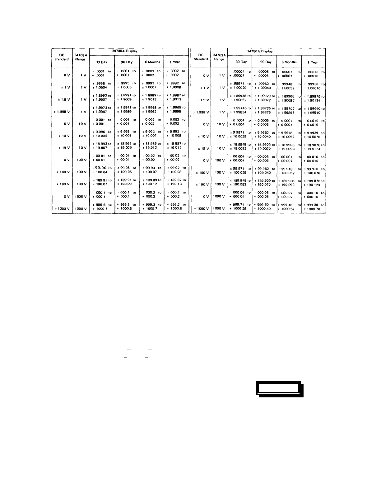
5-9 DC Accuracy
(30 Days)
1 V
Range
10V
Range
100 V
Range
1000 V
Range
(90 Days)
1 V
Range
10 V
Range
.0001
+ .9996
+ 1.8993
+ 1.9973
- 0.001
+ 9.996
+ 18.993
- 00.01
+ 99.96
+ 189.93
- .000.1
+ 999.6
- .0001
+ .9995
+ 1.8991
+ 1.9971
- 0.001
+ 9.996
+ 18.993
Results
_______________
_______________
_______________
_______________
_______________
_______________
_______________
_______________
_______________
_______________
_______________
_______________
_______________
_______________
_______________
_______________
_______________
_______________
+ .0001
+ 1.0004
+ 1.9007
+ 1.9987
+ 0.001
+ 10.004
+ 19.007
+ 00.01
+ 100.04
+ 190.07
+ .0001
+ 1.0004
+ .0001
+ 1.0005
+ 1.9009
+ 1.9989
+ 0.001
+ 10.004
+ 19.007
100 V
Range
1000 V
Range
(6 months)
1 V
Range
10 V
Range
100 V
Range
1000 V
Range
5-10
- 00.01
+ 99.96
+ 189.93
- 000.1
+ 999.5
- .0002
+ .9993
+ 1.8989
+ 1.9968
- 0.002
+ 9.993
+ 18.989
- 00.02
+ 99.93
+ 189.89
- 000.2
+ 999.3
_______________
_______________
_______________
_______________
_______________
_______________
_______________
_______________
_______________
_______________
_______________
_______________
_______________
_______________
_______________
_______________
_______________
+ 00.01
+ 100.04
+ 190.07
+ 000.1
+ 1000.5
+ .0002
+ 1.0007
+ 1.9012
+ 1.9992
+ 0.002
+ 10.007
+ 19.012
+ 00.02
+ 100.07
+ 190.12
+ 000.2
+ 1000.7
Page 34

Paragraph
Number Test Minimum
5-9 (Cont’d)
5-10
5-11
5-12 Normal Mode
5-13
(1 Year)
1 V
Range
10 V
Range
100 V
Range
1000 V
Range
Input Impedence
1 V and 10 V Ranges
100 V Range
1000 V Range
Capacitance
DC Effective
Common Mode
Rejection _____________
Rejection
AC Accuracy
45 Hz to 20 kHz
(30 Days)
1 V
Range
10 V
Range
100 V
Range
1000 V
Range
(90 Days)
1 V
Range
10 V
Range
100 V
Range
- .0002
+ .9992
+ 1.8987
+ 1.9966
- 0.002
+ 9.992
+ 18.987
- 00.02
+ 99.92
+ 189.87
- 000.2
+ 999.2
.5258
50.20
499.7
. 9970
1.8948
1.9845
9.970
18.948
99.70
189.48
000.5
997.0
.9965
1.8938
1.9835
9.965
18.938
99.65
189.38
TM 11-6625-2809-14 & P
Results
Actual Maximum
_____________
_____________
_____________
_____________
_____________
___
_____________
_____________
_____________
____________
_____________
_____________
_____________
____________
_____________
_____________
_____________
_____________
_____________
_____________
_____________
_____________
_____________
_____________ <10 counts
_____________
_____________
_____________
_____________
_____________
___
_____________
_____________
_____________
____________
_____________
_____________
_____________
____________
_____________
_____________
________
_____________
_____________
_____________
_____________
_____________
___
_____________
_____________
_____________
____________
_____________
_____________
+ .0002
+ 1.0008
+ 1.9013
+ 1.9994
+ 0.002
+ 10.008
+ 19.013
+ 00.02
+ 100.08
+ 190.14
+ 000.2
+ 1000.8
.5268
50.30
500.7
<80 pF
<10 counts
.0005
1.0030
1.9053
1.9955
0.005
10.030
19.053
00.05
100.30
190.53
000.5
1003.0
.0005
10.035
1.9062
1.9965
0.005
10.035
19.062
00.05
100.35
190.62
Rev. A 5-11
Page 35

TM 11-6625-2809-14 & P
Paragraph
Number Test Minimum Actual Maximum
5-13 (Cont’d)
100 V
Range
(6 Months)
1 V
Range
10 V
Range
100 V
Range
1000 V
Range
(1 Year)
1 V
Range
10 V
Range
100 V
Range
1000 V
Range
AC Accuracy
100 kHz
(30 Days)
1 V
Range
10 V
Range
100 V
Range
1000 V
Range
(90 Days)
1 V
Range
996.5
.9960
1.8929
1.9825
9.960
18.929
99.60
189.29
994.5
.9945
1.8900
9.945
18.900
99.45
189.00
994.5
.9920
1.8853
9.920
18.853
99.20
188.53
992.0
.9915
1.8839
Results
_______________
_______________
____
_______________
_______________
_______________
_______________
________
_______________
_______________
_______________
______
_______________
_______________
_______________
______
_______________
_______________
_______________
_______________
_______________
_______________
_______________
_______________
_______________
_______________
______
_______________
_______________
_______________
_______________
_______________
_______________
_______________
____
_______________
_______________
_______________
______
_______________
_______________
_______________
_______________
000.5
1003.5
.0005
1.0040
1.9072
1.9975
0.005
10.040
19.072
00.05
100.40
190.72
000.5
1005.5
.0005
1.0055
1.9100
0.005
10.055
19.100
00.05
100.55
191.00
000.5
1005.5
.0005
1.0080
1.9148
0.005
10.080
19.148
00.05
100.80
191.48
000.5
1008.0
.0005
1.0085
1.9162
5-12
Page 36

TM 11-6625-2809-14 & P
Paragraph
Number
5-13 (Cont’d)
Test Minimum Actual Maximum
10 V
Range
100 V
Range
1000 V
Range
(6 Months
1 V
Range
10 V
Range
100 V
Range
1000 V
Range
(1 Year)
1 V
Range
9.915
18.839
99.15
188.39
991.5
.9910
1.8819
9.910
18.829
99.10
188.29
991.0
.9895
1.8801
Results
________________
________________
________________
________________
________________
________________
________________
________________
________________
________________
________________
________________
________________
________________
________________
________________
________________
________________
________________
________________
________________
________________
0.005
10.085
19.162
00.05
100.85
190.16
000.5
1008.5
.0005
1.0090
1.9171
0.005
10.090
19.171
00.05
100.90
191.71
000.5
1009.0
.0005
1.0105
1.9200
10 V
Range
100 V
Range
1000 V
Range
5-14 Response Time _______________ < 30 counts
5-15
Ω Accuracy
(30 Day)
100 Ω
Range
1 κΩ
Range
10 κΩ
Range
9.895
18.801
98.95
188.01
989.5
99.93
189.89
.9993
1.8989
1.9888
9.993
18.989
________________
________________
________________
________________
________________
________________
________________
________________
________________
________________
________________
________________
________________
________________
________________
________________
________________
________________
0.005
10.105
19.200
00.05
101.05
192.00
000.5
1010.5
00.02
100.07
190.12
.0002
1.0007
1.9012
1.9912
0.002
10.007
19.912
5-13
Page 37

TM 11-6625-2809-14 & P
Paragraph
Number Test Minimum Actual Maximum
5-15 (Cont’d)
100 κΩ
Range
1000 κΩ
Range
10 ΜΩ
Range
(90 Day)
100 Ω
Range
1 κΩ
Range
10 κΩ
Range
100 κΩ
Range
1000 κΩ
Range
10 ΜΩ
Range
(6 Months)
100 Ω
Range
1 κΩ
Range
10 κΩ
Range
100 κΩ
Range
1000 κΩ
Range
10 ΜΩ
Range
99.93
189.89
999.3
1898.9
9.973
99.92
189.87
.9992
1.8987
1.9886
9.992
18.987
99.92
189.87
999.2
1898.7
9.973
99.90
189.84
.9990
1.8984
1.9883
9.990
19.883
99.90
198.83
999.0
1988.3
9.961
Results
________________
________________
________________
________________
________________
________________
________________
________________
________________
________________
________________
________________
________________
________________
________________
________________
________________
________________
________________
________________
________________
________________
________________
________________
________________
________________
________________
________________
________________
________________
________________
________________
________________
________________
________________
________________
________________
________________
________________
________________
________________
________________
________________
00.02
100.07
199.12
000.2
1000.7
1991.2
0.002
10.027
00.02
100.08
190.13
.0002
1.0008
1.9013
1.9914
0.002
10.008
19.013
00.02
100.08
190.13
000.2
1000.8
1901.3
0.002
10.027
00.03
100.10
190.16
.0003
1.0010
1.9016
1.9917
0.002
10.010
19.917
00.03
100.10
199.17
000.3
1001.0
1991.7
0.003
10.038
5-14
Page 38

TM 11-6625-2809-14 & P
Paragraph
Number Test Minimum Actual Maximum
5-15 (Cont’d) (1 Year)
100 Ω
Range
1 κΩ
Range
10 κΩ
Range
100 κΩ
Range
1000 κΩ
Range
10 ΜΩ
Range
99.86
189.76
.9986
1.8976
1.9875
9.986
18.976
99.86
189.76
998.86
1897.6
9.947
Results
________________
________________
________________
________________
________________
________________
________________
________________
________________
________________
________________
________________
________________
00.03
100.14
190.24
.0003
1.0014
1.9024
1.9925
0.003
10.014
19.024
00.03
100.14
190.24
000.3
1001.4
1902.4
0.003
10.053
5-15
Page 39

TM 11-6625-2809-14 & P
PERFORMANCE TEST CARD
Hewlett-Packard Model 34750A/34702A
Multimeter Tests Performed by________________
Serial No.________________________ Date___________________________
Paragraph
Numger Test Minimum Actual Maximum
5-9 DC Accuracy
(30 Days)
1 V
Range
10 V
Range
100 V
Range
1000 V
Range
(90 Days)
1 V
Range
10 V
Range
- .00004
+ .99971
+1.89948
+1.99746
- 0.0004
+ 9.9971
+18.9948
- 00.004
+ 99.971
+189.948
- 000.04
+ 999.71
- .00005
+ .99960
+1.89929
+1.99725
- 0.0005
+ .99960
+18.9929
Results
________________
________________
________________
________________
________________
________________
________________
________________
________________
________________
________________
________________
________________
________________
________________
________________
________________
________________
________________
+ .00004
+1.00029
+1.90052
+1.99854
+ 0.0004
+10.0029
+19.0052
+ 00.004
+100.029
+190.052
+ 000.04
+1000.29
+ .00005
+1.00040
+1.90072
+1.99875
+ 0.0005
+10.0040
+19.0072
100 V
Range
1000 V
Range
(6 Months)
1 V
Range
10 V
Range
100 V
Range
1000 V
Range
5-16
- 00.005
+ 99.960
+189.929
- 000.05
+ 999.60
- .00007
+ .99948
+1.89908
+1.99703
- 0.0007
+ 9.9948
+18.9908
- 00.007
+ 99.948
+189.908
- 000.07
+ 999.48
________________
________________
________________
________________
________________
________________
________________
________________
________________
________________
________________
________________
________________
________________
________________
________________
________________
+ 00.005
+100.040
+190.072
+ 000.05
+10000.40
+ .00007
+1.00052
+1.90093
+1.99897
+ 0.0007
+10.0052
+19.0093
+ 00.007
+100.052
+190.093
+ 000.07
+1000.52
Page 40

TM 11-6625-2809-14 & P
Paragraph
Number Test Minimum Actual Maximum
5-9 (Cont’d)
5-10 Input Impedance: Resistance
5-11 DC Effective
5-12
5-13 AC Accuracy
(1 Year)
1 V
Range
10 V
Range
100 V
Range
1000 V
Range
1 V and 10 V Rangers
100 V Ranges
1000 V Ranges
Capacities
Common Mode
Rejection
Normal Mode
Rejection ________________ < 100 counts
45 Hz to 20 kHz
(30 Days)
1 V
Range
- .00010
+ .99930
+1.89876
+1.99660
- 0.0010
+ 9.9930
+18.9876
- 00.010
+ 99.930
+189.876
- 000.10
+ 999.30
.52582
50.201
499.75
.99710
1.89485
1.98463
Results
________________
________________
________________
________________
________________
________________
________________
________________
________________
________________
________________
________________
________________
________________
________________
________________
________________ < 100 counts
________________
________________
________________
________________
+ .00010
+1.00070
+1.90124
+1.99940
+ 0.0010
+10.0070
+19.0124
+ 00.010
+100.070
+190.124
+ 000.10
+1000.70
.52682
50.301
500.75
< 80 pF
.00040
1.00290
1.90515
1.99538
10 V
Range
100 V
Range
1000 V
Range
(90 Days)
1 V
Range
10 V
Range
100 V
Range
Rev. A 5-17
9.9710
18.9485
99.710
189.485
997.10
.99650
1.89380
1.98353
9.9650
18.9380
99.650
189.380
________________
________________
________________
________________
________________
________________
________________
________________
________________
________________
________________
________________
________________
________________
________________
________________
________________
0.0040
10.0290
19.0515
00.040
100.290
190.515
000.40
1002.90
.00050
1.00350
1.90620
1.99647
0.0050
10.0350
19.0620
00.050
100.350
190.620
Page 41

TM 11-6625-2809-14 & P
Paragraph
Number Test Minimum Actual Maximum
5-13 (Cont’d)
1000 V
Range
(6 Months)
1 V
Range
10 V
Range
100 V
Range
1000 V
Range
(1 Year)
1 V
Range
10 V
Range
996.50
.99600
1.89285
1.98254
9.9600
18.9285
99.600
189.285
996.00
.99550
1.89000
9.9550
18.9000
Results
________________
________________
________________
________________
________________
________________
________________
________________
________________
________________
________________
________________
________________
________________
________________
________________
________________
________________
________________
________________
000.50
1003.50
.00050
1.00400
1.90715
1.99747
0.0050
10.0400
19.0715
00.050
100.400
190.715
000.50
1004.00
.00050
1.00550
1.91000
0.0050
10.0550
19.1000
100 V
Range
1000 V
Range
AC Accuracy
100 kHz
(30 Days)
1 V
Range
10 V
Range
100 V
Range
1000 V
Range
Rev. A. 5-18
99.550
189.000
995.50
.99200
1.88525
9.9200
18.8525
99.200
188.525
992.00
________________
________________
________________
________________
________________
________________
________________
________________
________________
________________
________________
________________
________________
________________
________________
________________
00.050
100.550
191.000
000.50
1005.50
.00050
1.00800
1.91475
0.0050
10.0800
19.1475
00.050
100.800
191.475
000.50
1008.00
Page 42

TM 11-6625-2809-14 & P
Paragraph
Number
5-13 (Cont’d)
Test
(90 Days)
1 V
Range
10 V
Range
100 V
Range
1000 V
Range
(6 Months)
1 V
Range
10 V
Range
100 V
Range
Results
Minimum Actual Maximum
.99150
1.88430
9.9150
18.8430
99.150
188.430
991.50
.99100
1.88335
9.9100
18.8335
99.100
188.335
______________
______________
______________
______________
______________
______________
______________
______________
______________
______________
______________
______________
______________
______________
______________
______________
______________
______________
______________
______________
.00050
1.00850
1.91570
0.0050
10.0850
19.1570
00.050
100.850
191.570
000.50
1008.50
.00050
1.00900
1.91665
0.0050
10.0900
19.1665
00.050
100.900
191.665
1000 V
Range
(1 Year)
1 V
Range
10 V
Range
100 V
Range
1000 V
Range
5-14 Response Time ______________ < 300 counts
5-15
Ω Accuracy
(30 Day)
100 Ω
Range
1kΩ
Range
991.00
.98950
1.88050
9.8950
18.8050
98.950
188.050
989.50
99.940
189.900
.99940
1.89900
1.98895
______________
______________
______________
______________
______________
______________
______________
______________
______________
_____________
______________
______________
______________
______________
______________
______________
______________
000.50
1009.00
.00050
1.01050
1.91950
0.0050
1.01050
19.1950
00.050
101.050
191.950
000.50
1010.50
00.015
100.060
190.101
.00015
1.00060
1.90101
1.99105
5-19
Page 43

TM 11-6625-2809-14 & P
Paragraph
Number
5-15 (Cont’d)
Test
10 kΩ
Range
100 kΩ
Range
1000 kΩ
Range
10 MΩ
Range
(90 Day)
100 Ω
Range
1 kΩ
Range
10 kΩ
Range
100 kΩ
Range
1000 kΩ
Range
10 MΩ
Range
(6 Months)
100 Ω
Range
1 kΩ
Range
10 kΩ
Range
100 kΩ
Range
1000 kΩ
Range
Results
Minimum Actual Maximum
9.9940
18.9900
99.940
189.900
999.40
1899.00
.99940
99.930
189.881
.99930
1.89881
1.98891
9.9930
18.9881
99.930
189.881
999.30
1898.81
.99685
99.915
189.877
.99915
1.89877
1.98871
9.9915
18.9877
99.915
189.877
998.70
1897.71
___________________
___________________
___________________
___________________
___________________
___________________
___________________
___________________
___________________
___________________
___________________
___________________
___________________
___________________
___________________
___________________
___________________
___________________
___________________
___________________
___________________
___________________
___________________
___________________
___________________
___________________
___________________
___________________
_____________
___________________
___________________
___________________
___________________
___________________
___________________
___________________
___________________
___________________
___________________
___________________
___________________
___________________
___________________
___________________
___________________
0.0015
10.0060
19.0101
00.015
100.060
190.101
000.15
1000.60
1901.01
0.0015
1.00060
00.015
100.070
190.120
.00015
1.00070
1.90120
1.99109
0.0015
10.0070
19.0120
00.015
100.070
190.124
000.15
1000.70
1901.20
0.0015
1.00315
00.020
100.085
190.124
.00020
1.00085
1.90124
1.99129
0.0020
10.0085
19.0124
00.020
100.085
190.124
000.20
1001.30
1902.29
5-20
Page 44

TM 11-6625-2809-14 & P
Paragraph
Number
5-15 (Cont’d)
Test
10 MΩ
Range
(1 Year)
100 Ω
Range
1 kΩ
Range
10 kΩ
Range
100 kΩ
Range
1000 kΩ
Range
10 MΩ
Range
Results
Minimum Actual Maximum
.99630
99.870
189.771
.99870
1.89771
1.98761
9.9870
18.9771
99.870
189.771
998.70
1897.71
.99480
_________________
_________________
__
_________________
_________________
_________________
___
_________________
_________________
_________________
_________________
____
_________________
_________________
_________________
___
_________________
_________________
_________________
___
_________________
_________________
_________________
___
0.0020
1.00370
00.020
100.130
190.229
.00020
1.00130
1.90229
1.99239
0.0020
10.0130
19.0229
00.020
100.130
190.229
000.20
1001.30
1902.39
0.0020
1.00520
5-21
_________________
_________________
__
Page 45

Model 34702AT TM 11-6625-2809-14 & P
SECTION VI.
IDENTIFICATION OF PARTS
6-1. INTRODUCTION.
6-2. This section contains information to identify parts.
Table 6-1 lists parts in alphanumeric order of their
reference designators and indicates the desc ription, -hpPart Number of each part, together with any applicable
notes, and provides the following:
a. Total quantity used in the instrument (Qty
column). The total quantity of a part is given the first
time the part number appears.
b. Description of the part. (See list of
abbreviations below.)
c. Typical manufacturer of the part in a fivedigit code.
d. Manufacturers part number.
6-3. Miscellaneous parts are listed at the end of Table
6-1.
6-4 DELETED
6-5 DELETED
6-6. DELETED
6-7. DELETED
6-8. PARTS CHANGES
6-9. Components which have been changed are so
marked by one of three symbols; i.e. ∆, ∆ with a letter
subscript, e.g.
, or ∆ with a number subscript e.g.
∆
a
∆
10
A ∆ with no subscript indicates the component listed is
the preferred replacement for an earlier component. A
with a letter subscript indicates a change which is
explained in a note at the bottom of the page. A ∆ with a
number subscript indicates the related change is
discussed in backdating (Appx A). The number of the
subscript indicates the number of the change in
backdating which should be referred to.
.
∆
6-10.PROPRIETARY PARTS.
6-11.Items marked by a dagger (†) in the reference
designator column are available only for repair and
service of Hewlett-Packard instruments.
6-1
Page 46

Model 34702AT TM 11-6625-2809-14 & P
6-2
Page 47

Model 34702A TM 11-6625-2809-14 & P
Table 6-1. Identification of Parts
Rev. A 6-3
Page 48

Model 34702A TM 11-6625-2809-14 & P
Table 6-1. Identification of Parts
6-4
Page 49

Model 34702A TM 11-6625-2809-14 & P
Table 6-1. Identification of Parts
Rev. A 6-5
Page 50

Model 34702A TM 11-6625-2809-14 & P
PART NUMBER - NATIONAL STOCK NUMBER
CROSS REFERENCE INDEX
NATIONAL NATIONAL
PART STOCK PART STOCK
NUMBER FSCM NUMBER NUMBER FSCM NUMBER____
CB-36G5 01121 5905-00-458-4406 1810-0173 28480 5905-01-042-5043
CB2721 01121 5905-00-111-4727 1820-0203 28480 5962-00-483-1956
CB6821 01121 5905-00-721-0671 1820-0571 28480 5962-00-329-4583
DM74LO2N 12040 5962-00-257-9226 1820-0583 28480 5962-00-390-7958
DM74L74N 12040 5962-00-369-7607 1820-0586 28480 5962-00-390-7970
DM74L86N 12040 5962-00-172-5578 1820-0587 28480 5962-00-396-2262
RDM15F391-J3C 72136 5910-00-018-0918 1820-0635 28480 5962-00-329-4569
SL8940 07263 5962-00-483-1956 1820-0668 28480 5962-00-369-9839
SN74175N 01295 5962-00-163-0145 1853-0010 28480 5961-00-931-6998
SZ10939-122 04713 5961-00-752-6121 1853-0089 28480 5961-00-179-8478
SZ10939-98 04713 5961-00-821-2309 1854-0039 28480 5961-00-985-9073
0121-0127 28480 5910-00-828-2061 1854-0404 28480 5961-00-408-9807
0121-0168 28480 5910-00-244-8375 1901-0029 28480 5961-00-950-0537
0140-0145 28480 5910-00-257-0227 1902-0040 28480 5961-00-059-1215
0140-0196 28480 5910-00-774-7294 1902-0041 28480 5961-00-858-7372
0140-0204 28480 5910-00-069-0362 1902-0049 28480 5961-00-911-9277
0150-0014 28480 5910-00-834-5013 1902-3149 28480 5961-00-833-3043
0160-3930 28480 5910-00-378-0588 1902-3182 28480 5961-00-229-1966
0170-0022 28480 5910-00-826-1162 192P39292-PTS 56289 5910-00-921-0275
0170-0038 28480 5910-00-817-7275 193-0010-005 74970 5910-00-378-0646
0170-0040 28480 5910-00-829-0245 1990-0413 28480 5961-01-042-5332
0170-0043 28480 5910-00-993-8535 2N4117A 80131 5961-01-017-6023
0180-0197 28480 5910-00-850-5355 2100-3154 28480 5905-00-615-8111
0180-0291 28480 5910-00-931-7055 3101-1723 28480 5930-01-035-8847
0180-1800 28480 5910-00-126-1696 312.500 75915 5920-00-280-8344
0340-0782 28480 5970-01-025-0262 8131-100-651-104 72982 5910-00-451-5671
0370-2159 28480 5975-01-007-9111 9100-3223 28480 5950-01-042-1970
0683-1025 28480 5905-00-110-7620
0683-1525 28480 5905-00-106-1356
0684-1021 28480 5905-00-056-0531
0684-1051 28480 5905-00-116-8554
0684-1221 28480 5905-00-407-2151
0684-2221 28480 5905-00-105-7764
0684-2731 28480 5905-00-119-3504
0684-3921 28480 5905-00-141-0743
0687-1201 28480 5905-00-110-0196
0698-3152 28480 5905-00-420-7130
0698-3159 28480 5905-00-407-0053
0698-3243 28480 5905-00-891-4227
0698-3264 28480 5905-00-138-5051
0698-3274 28480 5905-00-483-0226
0698-3437 28480 5905-00-402-7080
0698-3499 28480 5905-00-478-7468
0698-3515 28480 5905-00-478-7469
0698-3558 28480 5905-00-407-0061
0698-3700 28480 5905-00-138-5052
-698-4123 28480 5905-00-998-1915
0698-4470 28480 5905-00-759-1539
0698-6391 28480 5905-00-306-0740
0757-0443 28480 5905-00-891-4252
0757-0451 28480 5905-00-981-7478
0757-0461 28480 5905-00-089-7577
0757-0486 28480 5905-00-982-3777
0813-0032 28480 5905-00-490-3946
1N825 04713 5961-00-923-3940
150D105X9035A2-D 56289 5910-00-456-4474
1510-0091 28480 5940-01-035-6148
1810-0151 28480 5905-01-023-2750
1810-0171 28480 5905-01-042-7499
1810-0172 28480 5905-01-043-0514
6-6
Page 51

Model 34702A TM 11-6625-2809-14 & P
SECTION VII.
TROUBLESHOOTING AND
CIRCUIT DIAGRAMS
7-1. INTRODUCTION.
7-2. This section of the Operating and Service
Manual contains troubleshooting information and circuit
diagrams for the Model 34702A Multimeter. Included are
trouble shooting trees, a schematic diagram and a
component locator.
7-3. SCHEMATIC DIAGRAM.
74. The circuits contained within the Model 34702A
are shown on the schematic diagram (F igure 7-3). This
diagram can be used to assist in understanding of the
theory of operation as well as aid in troubleshooting the
instrument. DC voltages and ac waveforms are given on
the schematic.
7-5. COMPONENT LOCATION DIAGRAM.
7-6. The Component Location Diagram associated
with the schematic shows the position of each part
mounted on the pc assembly. Each part is identified by a
reference designator.
7-7. TROUBLESHOOTING.
7-8. Troubleshooting Trees.
7-9. Figures 7-1 and 7-2 are troubleshooting trees
designed to assist in the isolation of malfunctions.
Figure 7-1 is a troubleshooting tree for the ac converter ,
Figure 7-2 is a troubleshooting tree for the Ω converter.
7-10. Troubleshooting Procedure.
7-11. The following procedure is recommended for
troubleshooting the Model 34702A:
a. Ensure the mainframe plug-on (Display
Module) is functioning properly.
b. Perform the following preliminary tests:
1. Apply t 1.0000 V dc to the INPUT V
terminals. Check for turnover error.
2. Apply full-scale voltages to the 10 V,
100 V, and 1000 V scales. Check for
proper numerical display and decimal
point location.
NOTE
The above checks verify proper
functioning of many display module
interconnections, range switches, and
coaxial wiring.
c. Check the ac converter as follows:
1. Apply I V ac at 01kHz to the INPUT V
terminals.
2. Trace the propagation of this signal through
the impedance converter, ac converter
amplifier and filter circuitry.
3. If these circuits appear to be working, check
the Input Attenuator.
(a)Apply full-scale voltages to the 34702A
on the IO V, 100 V, and 1000 V
ranges. Do this at 10 kHz and 100
kHz.
(b)Note any inaccuracies in the readout.
Any error is probably due to the input
attenuator.
NOTE
Most frequency response problems are
in the input attenuator.
4. Typical Problem Areas.
(a)Noise-check ac converter amplifier.
(b)Low output or zero output-check the ac
converter amplifier.
(c)Any type of inaccuracy-check dc
feedback amplifier Ul by replacement.
Also, check Q1 for leakage (by
replacement).
d. Check the dc section of the instrument:
1. Check for shorted trimmer capacitors.
2. Using an Ωmeter, measure the contact
resistance of the switches. Each switch
should indicate a short circuit. Dirty
switches can be cleaned with MS-1 80
Freon Degreaser.
3. Coax cables may be shorted or open.
4. Resistors in the dc attenuator may change
value.
e. Check the ohms current source:
1. Place the 34702A in Ω function and verify
that an overload indication occurs
(overrange "1" illuminates and rest of
display blanks) with no resistance applied.
7-1
Page 52

Model 34702A TM 11-6625-2809-14 & P
2. Check all ohms ranges at full-scale to
determine which ranges are bad. When
only the two highest ranges are inaccurate,
check Q11 if the display indication is high.
Check CR13 if the indication is low.
3. Referring to the schematic diagram, check
the voltages on the two operational
amplifiers. If the- 7.2 V and - 6.2 V
references are incorrect or absent, check
U3 and CR16.
f. Attempt the Performance Tests (Section V) in
order to characterize the trouble. Also try the Adjustment
Procedures. Some apparent malfunctions can be
corrected by these adjustments. Als o, inability to obtain
correct adjustment will help localize the problem.
g. Check for burned or loose components,
loose connections, or other conditions which might be
the source of the trouble.
h. If the problem exists on the DCV and ACV
functions but not on the Ω function, troubleshoot the
DCV/ACV attenuator. If the trouble exists only on the
or ACV function, refer to the respective troubleshooting
tree.
Ω
7-2
Page 53

Model 34702A TM 11-6625-2809-14 & P
APPENDIX A
DATA DIFFERENCE SHEET
A-1. INTRODUCTION.
A-2. This section makes your manual applicable to
earlier instruments. Where component values or part
numbers in an instrument differ from the replaceable
parts list, yet are not listed in this section, the part
numbers and values listed in the parts list should be
used for replacement.
A-3. Where practical, backdating entries have been
incorporated into the text of the manual r ather than into
this section. If a backdating change is too long or
otherwise impractical to incorporate in the text, the entr y
to be changed will be flagged with a delta having a
). The subscript refers to the
number subscript; e.g. (
∆
1
number of the corresponding change in backdating.
Make all changes listed in this back dating which apply to
your instrument.
∆
CHANGE NO.
: Applies to serial numbers
1
1212A0335 and below
Table 6-1:
Delete A1C31, A1R68, and A1C8
Change A1C12 to C:fxd, .01 µF + 20%
2000 vdcw, -h p-Part No. 0160-0996
Figure 7-3, Page 7-5 & 7-6:
Change the input circuit to AIQI as follows:
Change the component locator for the
A1 Assembly as follows:
3470A-B-2990
A1
hp Part No. 34702-66501
A-1
Page 54

APPENDIX B
REFERENCES
DA Pam 310-4 Index of Technical Manuals, Technical Bulletins,
Supply Manuals, (Type 7, 8, and 9), Supply
Bulletins, and Lubrication Orders.
DA Pam 310-7 US Army Equipment Index of Modification Work Orders.
TM 38-750 The Army Maintenance Management System (TAMMS).
TM 740-90-1 Administrative Storage of Equipment.
TM 750-244-2 Procedures for Destruction of Electronics Materiel
to Prevent Enemy Use (Electronics Command).
B-1
TM 11-6625-2809-14 & P
Page 55

TM 11-6625-2809-14 & P
APPENDIX C
MAINTENANCE ALLOCATION
_________________________________________________________________________________________________
Section I. INTRODUCTION
C-1. General
This appendix provides a summ ary of the maintenance
operations for ME-498/U. It authorizes categories of
maintenance for specific maintenance functions on
repairable items and components and the tools and
equipment required to perform each function. This
appendix may be used as an aid in planning
maintenance operations.
C-2. Maintenance Function
Maintenance functions will be limited to and defined as
follows:
a. Inspect.
an item by comparing its physical, mechanical, and/or
electrical characteristics with established standards
through examination.
b. Test.
incipient failure by measuring the mechanical or
electrical characteristics of an item and compar ing those
characteristics with prescribed standards.
c. Service.
keep an item in proper operating c ondition; i.e, to clean
(decontaminate), to preserve, to drain, to paint, or to
replenish fuel, lubricants, hydraulic fluids, or com pres sed
air supplies.
d. Adjust.
limits, by brining into proper or exact position, or by
setting the operating characteristics to the specified
parameters.
e. Align.
of an item to bring about optimum or desired
performance.
f. Calibrate.
corrections to be made or to be adjus ted on instruments
or test measuring and diagnostic equipments used in
precision measurem ent. Consists of c om parisons of two
instruments, one of which is a certified standard of
known accuracy, to detect and adjust any discrepancy in
the accuracy of the instrument being compared,
g. Install.
fixing into position an item, part, m odule
assembly) in a manner to
the equipment or system.
To determine the ser viceability of
To verify serviceability and to detect
Operations required periodically to
To maintain, within prescribed
To adjust specified variable elements
To determine and cause
The act of emplacing, seating, or
(component or
allow the proper functioning of
h. Replace.
serviceable like type part, subassembly, or module
(component or assembly) for an unserviceable
counterpart.
i. Repair.
services (inspect, teste, service, adjust, align, calibrate,
replace) or other maintenance ac tions (welding, grinding,
riveting, straightening, facing, remachining, or
resurfacing) to restore serviceability to an item by
correcting specif ic damage, fault, malfunction, or failure
in a part, subassembly, module (component or
assembly), end item, or system.
j. Overhaul.
(service/action) necessary to restore an item to a
completely serviceable/operational condition as
prescribed by maintenance standards (i.e., DMWR) in
appropriate technical publications. Overhaul is normally
the highest degree of maintenance performed by the
Army. Overhaul does not normally return an item to lik e
new condition.
k. Rebuild.
necessary for the restoration of unserviceable equipm ent
to a like new condition in accordance with original
manufacturing standards . Rebuild is the highest degree
of materiel maintenance applied to Army equipment.
The rebuild operation includes the act of returning to zero
those age measurements ( hours, miles , etc.) considered
in classifying Army equipments/components.
C-3. Column Entries
a. Column 1, Group Number.
group numbers, the purpose of which is to identify
components, assemblies, subassemblies, and modules
with the next higher assembly.
b. Column 2, Component/Assembly.
2 contains the noun names of com ponents, assemblies,
subassemblies, and modules for which maintenance is
authorized.
c. Column 3, Maintenance Functions.
3 lists the functions to be perfor med on the item listed in
column 2. W hen items are listed without maintenance
functions, it is solely for purpose of having the group
The act of substituting a
The application of maintenance
That maintenance effort
Consists of those services /actions
Column 1 lists
Column
Column
C-1
Page 56

TM 11-6625-2809-14 & P
numbers in the MAC and RPSTL coincide.
d. Column 4, Maintenance Category.
Column
4 specifies, by the listing of a "work time" figure in the
appropriate subcolumn(s), the lowest level of
maintenance authorized to perform the function listed in
column 3. This figure represents the active time required
to perform that maintenance function at the indicated
category of maintenance. If the num ber or com plexity of
the tasks within the listed maintenance f unction vary at
different maintenance categories, appropriate" work
time" figures will be shown for each category. The
number of task-hours specified by the "work time" figure
represents the average time required to restore an item
(assembly, subassembly, com ponent, module, end item
or system) to a serviceable condition under typical field
operating conditions. This time includes preparation time,
troubleshooting time, and quality assurance/quality
control time in addition to the time required to perform
the specific tasks identified for the maintenance
functions authorized in the maintenance alloc ation chart.
Subcolumns of column 4 are as follows:
__
Operator/Crew
C
__
Organizational
O
__
Direct Support
F
__
General Support
H
__
Depot
D
e. Column 5, Tools and Equipment.
Column 5
specifies by code, those comm on tool sets ( not individual
tools) and special tools, test, and support equipment
required to perform the designated function.
f. Column 6, Remarks.
Not applicable.
C-4. Tool and Test Equipment Requirements
(Sec III)
a. Tool or Test Equipment Reference
Code.
The numbers in this column coincide with the
numbers used in the tools and equipm ent column of the
MAC. The numbers indicate the applicable tool or test
equipment for the maintenance functions.
b. Maintenance Category.
The codes in this
column indicate the maintenanc e category allocated the
tool or test equipment.
c. Nomenclature.
This column lists the noun
name and nomenclature of the tools and test equipm ent
required to perform the maintenance functions.
d. National/NATO Stock Number.
This
column lists the National/NATO stock number of the
specific tool or test equipment.
e. Tool Number.
This column lists the
manufacturer’s part number of the tool followed by the
Federal Supply Code for manufacturers(5-digit) in
parentheses.
C-5. Remarks (Sec IV)
Not applicable.
C-2
Page 57

TM 11-6625-2809-14 & P
SECTION II. MAINTENANCE ALLOCATION CHART
FOR
MUTIMETER ME-498/U
(1) (2) (3) (4) (5) (6)
GROUP COMPONENT/ASSEMBLY MAINTENANCE MAINTENANCE CATEGORY AND
NUMBER FUNCTION C O F H D EQPT REMARKS
00 MUTIMETER ME-498/U Inspect 0.2 6
MODEL 34702A Test 0.5 1 thru 5
DISPLAY MODEL Service 0.6 1 thru 5
Install 0.3 1 thru 5
Replace 0.3 1 thru 5
Repair 1.2 1 thru 5
Overhaul 2.0 1 thru 5
TOOLS
C-3
Page 58

TM 11-6625-2809-14 & P
SECTION III TOOL AND TEST EQUIPMENT REQUIREMENTS
FOR
MULTIMETER ME-498/U
TOOL OR TEST MAINTENANCE NATIONAL/ TOOL
EQUIPMENT CATEGORY NOMENCLATURE NATO STOCK NUMBER
REF CODE NUMBER
1 H, D AN/GSM-64 Digital Voltmeter Non Linear Systems V35A 6625-00-870-2264
2 H, D AN/USM-459 Frequency Counter HP 3662 6625-01-061-8928
3 H, D Resistor Decade ZM-16( )/U 6625-00-669-0266
4 0 Tools and test equipment available to the technician for his/her
assigned mission.
C-4
Page 59

TM 11-6625-2809-14 & P
APPENDIX D
OPERATOR’S, ORGANIZATIONAL, DIRECT SUPPORT, AND GENERAL SUPPORT
MAINTENANCE REPAIR PARTS AND SPECIAL TOOLS LIST
NOTE
Refer to section VI, Identification of Parts, for all maintenance repair parts.
D-1
Page 60

PART TWO
TM 11-6625-2809-14 & P
PRINTED IN U.S.A
Revised: March 1975 Printed: JUNE 1973
0-1
Page 61

Model 34750A TM 11-6625-2809-14 & P
SECTION I
GENERAL INFORMATION
1-1. DESCRIPTION.
1-2. The Hewlett-Packard Model 34750A Display
Module is part of the low cost 3470 Measurement
System designed to measure AC volts, DC volts, current
and resistance. It can be combined with the Model
34701 A, Model 34702A or Model 34703A Plug-On
Module, shown in Figure 1-1, to make these
measurements. Table 1-1 lists the various plug-on
34750
modules which condition the input to the Model
and indicates the functions of each.
A,
Figure 1-1. Plug-On Modules which can be used with the 34750A Display Module.
1-1
Page 62

Model 34750A TM 11-6625-2809-14 & P
Figure 1-2. Accessories Available for use with 34750A.
1-2
Page 63

Model 34750A TM 11-6625-2809-14 & P
Table 1-1. 3470A Series Signal Conditioning Modules.
Plug-On
(Signal Conditioning) Function
Module
DCV Ω ACV DCA Auto
Ranging
34701A
DC Voltmeter X
34702A
Multimeter X X X
34703A
DCV/DCA/Ω Meter X X X X
1-3. Two center (sandwich) modules are also
available for use with the Model 34750A and a signal
conditioning module. These modules (Model 34720A
and Model 34721A) add the capabilities of battery
operation and BCD output to the 3470A measurement
system. These modules are also shown in Figure 1-1.
1-4. The digital readout of the 34750A consists of five
full digits plus an overrange "1". The LED (Light Em itting
Diode) display provides a bright clear readout with a
maximum display of 199999.
1-5. The Model 34750A has an internal jumper wire
which may be positioned to test the logic and display
circuits.
1-6. SPECIFICATIONS.
1-7. Specifications for the 34750A are included in
Section I of the Operating and Service manuals for the
"plug-on" modules.
1-8. OPTIONS.
1-9. Options available for the 34750A are listed in
Table 1-2.
Table 1-2. Available Options.
Option Purpose
060
050
Operation with 60 Hz line.
Operation with 50 Hz line.
Measurement
Rate
5/sec
8/sec
1-10. ACCESSORIES AVAILABLE (See Figure 1-2).
a. 11456A - Read Out Test Card - Facilitates
testing and troubleshooting the Model 34750A Display
Module.
b. 18019A - Carrying Case - Accomm odates
the 34750A Display Module, a center module, and a "
plug-on" module plus the power cord and input cables.
c. 11457A - Rack Mount Kit-Permits rack
mounting of a 34750A Display Module, a 34721 B Center
Module, and a "plug-on" module.
d. 10576A - Rack Mount Kit- Permits rack
mounting of a 34750A Display Module and a "plug-on"
module.
e. 562A-16C - Printer Cable - Connects the
output of the Model 34721B BCD Module to
a Model 5055A Digital Recorder.
1-11. INSTRUMENT AND MANUAL
IDENTIFICATION.
1-12. A three-section serial number is used to identify
your Model 34750A. Figure 1-3 illustrates the meaning
of the three parts of the number.
1-13. This manual is kept up-to-date with revised
pages. If the serial number of your instrument is lower
than the one on the title page of this manual ref er to the
backdating inform ation in Appendix A which adapts this
manual to your instrument. All correspondence with
Hewlett-Packard Company should include the complete
serial number.
Figure 1-3. Instrument Serial Number (on rear panel).
1-3
Page 64

Model 34750A TM 11-6625-2809-14 & P
SECTION II.
INSTALLATION
2-1. INTRODUCTION.
2-6. The 34750A can be operated from the following
2-2. This section contains inform ation and instructions
for the installation and shipping of the 34750A. Included
are initial inspection procedures, power and grounding
requirements, environmental information and
repackaging for shipment.
2-3. INITIAL INSPECTION.
2-4. This instrument was carefully inspected both
mechanically and electrically before shipm ent. It should
be physically free of mars or scratches and in perfect
electrical order upon receipt. To confirm this, the
instrument should be inspected for physical damage
incurred in transit. If the instrument was damaged in
transit, file a claim with the carrier. Check to ensure you
have received a power cord with the instrument. Using
the performance test procedures referred to in Section V,
test the electrical performance of the ins trum ent. If there
is damage or deficiency see the warranty on the reverse
side of the title page of this manual.
nominal primary power sources:
Line Voltage Tolerances Frequency Range
100 V
120 V
220 V
240 V
The 34750A is set for 120 volt operation at the factory.
Refer to Figure 2-1 for the procedur e to change your unit
for operation on a different voltage.
+ 5% to - 10%
+ 5% to - 10%
+ 5% to - 10%
+ 5% to - 10%
48 to 440 Hz
48 to 440 Hz
48 to 440 Hz
48 to 440 Hz
IF THE INSTRUMENT IS NOT SET
FOR THE CORRECT PRIMARY
POWER VOLTAGE IT MAY BE
SERIOUSLY DAMAGED.
2-5. POWER REQUIREMENTS.
Figure 2-1. Voltage Selection.
2-1
Page 65

Model 34750A TM 11-6625-2809-14 & P
The primary power voltage that is currently selected to
operate your 34750A can be observed in the power
module window. (See Figure 2-1).
2-7. GROUNDING REQUIREMENTS.
2-8. To protect operating personnel, the National
Electrical Manufacturers’ Association (NEMA)
recommends that the instrument panel and cabinet be
grounded. The Model 34750A is equipped with a threeconductor power cable that grounds the instrument when
it is plugged into the appropriate receptacle. The offset
pin on the power cable is the ground wire.
2-9. To preserve this protection feature when
operating from a two-contact outlet, use a three-prong to
two- prong adapter and connect the pigtail on the
adapter to power line ground.
2-10. ENVIRONMENTAL REQUIREMENTS.
2-11. The 34750A should not be operated where the
ambient temperature exc eeds 00 C to 500 C (320 F to
1220° F) or stored where the ambient temperature
exceeds - 400 C to 750 C (- 400 F to 1670 F).
2-12. INSTRUMENT MOUNTING.
2-13. Bench Use.
2-14. The front of the 34750A may be elevated for
operating convenience by lowering the tilt stand on the
bottom module.
2-15. Rack Use.
2-16. Figure 2-2 shows the available kits for rack
mounting the various module com binations of the 3470
series of instruments.
2-17. REPACKAGING FOR SHIPMENT.
2-18. The following paragraphs contain a general
guide for repackaging the instrument for shipment.
Refer to Paragraph 2-19 if the original container is to be
used; 2-20 if it is not. If you have any questions, contac t
your nearest -hp- Sales and Service Office.
NOTE
If the instrument is to be shipped to
Hewlett-Packard for service or repair,
attach a tag to the instrument identifying
the owner and indicating the service or
repair to be accomplished. Include the
module number and full serial number of
the instrument. In any correspondence,
identify the instrument by model number
and full serial number.
2-19. Place the instrument in the original container
with appropriate packing material and seal well with
strong tape or metal bands.
Figure 2-2. Rack Mount Kits
2-20. If the original container is not to be used,
proceed as follows:
a. Wrap the instrument in heavy paper or
plastic before placing in an inner container.
b. Place the packing material around all sides
of the instrument and protect the panel face with
cardboard strips.
2-2
Page 66

Model 34750A TM 11-6625-2809-14 & P
c. Place instrument and inner container in a
heavy carton or wooden box and seal with strong tape or
metal bands.
2-21. POWER CORDS AND RECEPTACLES.
2-22. Figure 2-3 illustrates power receptacle (wall
outlet) configurations that are used throughout the United
States and in other countries. The -hp- part number
shown directly below each receptacle drawing is the part
number for a 34750A power cord equipped with the
appropriate mating plug for that receptacle. If the
appropriate power cord is not included with the
instrument, notify the nearest -hp- Sales and Service
Office and a replacement cord will be provided. The
34750A power cord, power input receptacle and mating
connectors meet the safety standards set forth by the
International Electrotechnical Commission (IEC).
Figure 2-3. Power Receptacles.
Rev. A 2-3
Page 67

Model 34750A TM 11-6625-2809-14 & P
SECTION III.
OPERATING INSTRUCTIONS
3-1. INTRODUCTION.
3-2. This section contains instructions and
information which will assist you in proper operation of
your Model 34750A Display Module. A signal
conditioning module (Model 34701A, 34702A or 34703A)
is required for proper operation of the display module.
3-3. REAR PANEL FEATURES.
3-4. The rear panel of the Model 34750A is shown in
Figure 3-1.
DO NOT PLUG IN THE POWER CORD
WITHOUT FIRST SELECTING THE
PROPER LINE VOL TAGE.
3-5 WARM-UP.
3-6. A warm-up period of 1 hour is normally required
for the instrument to achieve specified accuracy. The
instrument should be calibrated with the bottom and
center modules to be used with the instrument.
NOTE
Due to temperature change inside the
instrument between line and battery
operation, the + and - references must
be readjusted when changing modes to
achieve specified accuracy. The
nominal temperature change between
line and battery operation is - 150 C
3-7. OPERATION WITH PLUG-ON MODULES.
3-8. Information regarding operation of the
instrument with a plug-on module can be found in the
Operating and Service Manual for the plug-on.
Figure 3-1. 34750A Rear Panel.
INSTALLATION OR REMOVAL OF PLUG-ON
MODULES IS TO BE MADE BY QUALIFIED
PERSONNEL ONLY.
Rev. A 3-1
Page 68

Model 34750A TM 11-6625-2809-14 & P
1. This measurement exam ple is for a dc voltage of + 1.2 volts m easur ed on the 1 volt r ange of an -hp- Model 34701A.
For this measurement the voltage at A and B is + 1.2 volts for the entire measurement sequence.
2. Prior to to (during 5TO of the previous measurement) SA was connected to ground and SB was closed. The Auto-Zero
circuit was enabled and a voltage applied to the + input of the Integrator Am plifier ( point F) that caus es the voltage at
E to be 0 volts. This voltage will stay at F until the Auto-Zero circuit is-again enabled after the value of the input
voltage has been determined.
3. At to, SA is switched to the output of the signal conditioning unit and the Input Amplif ier is given tim e to respond to its
new value during OT1. SB is open during this time interval so the output of the Integrator remains at 0 volts.
4. SB is closed at t1 and the Integrator output ramps to a level proportional to the input voltage during 1T2.
5. The output level of the Integrator remains c onstant during 2T3 because SB opens at t2. SA is switched to one of the
reference voltage positions (- Ref. for a + voltage at B) and the Input Amplifier Is given time to achieve its new
output level.
6. During 3T4 and 4T5, SB is closed and the Integrator output ramps toward 0 volts. When zero detect occurs SA is
switched to ground and the Auto-Zero circuits are enabled. Dur ing the time interval from t3 until zero detect occurs
the output of a fixed frequency oscillator is c ounted. T he c ounts ac cumulated during this time interval are trans f err ed
to storage buffers and displayed as measured result on the front panel.
7. The auto-zero cycle begins at zero detect. Zero detect can occur as late as t
The time interval 5TO provides
5.
adequate time for the Auto-Zero circuits to complete the auto-zero cycle.
Figure 4-1. Basic Block Diagram of 34750A
Rev. B 4-0
Page 69

Model 34750A TM 11-6625-2809-14 & P
SECTION IV
THEORY OF OPERATION
waveforms and a timing s equence in Figure 4-1. Each
4-1. INTRODUCTION.
4-2. The 34750A Display is a five-digit analog-todigital converter that utilizes the dual slope integrating
technique and a LED (light-emitting diode) display. The
34750A is designed to operate with a signal-conditioning
"Plug-On Module". The signal-conditioning unit c onverts
the input signal to a dc voltage between + 2 volts (+
volt full scale + 100% overrange) which is measur ed and
displayed by the 34750A. A Basic Block Diagram of the
34750A (Figure 4-1) will be discussed in this section
followed by a more detailed description of thes e blocks
and the circuits involved.
4-3. Basic Measurement Sequence.
4-4. The dual slope integrating measurement
technique employed by the 34750A is described with
1
measurement sequenc e is divided into six time intervals
of equal length. Figure 4-1 shows the designations that
will be used to identify the beginning of each time
interval, the time intervals and a description of the
measurement cycle.
4-5. ANALOG CIRCUITS.
4-6. Input Amplifier.
4-7. A stable gain of + 3.5 is provided by the Input
Amplifier (see Figure 4- 2). O nly one of the FET switches
Q1 through Q4 is conducting at a time to provide an
input to the amplifier. Bias current is minimized by the
FET input stage of the amplifier. Adjustm ent R8 sets the
output at TP1 to 0 V with point 1 grounded. The FET
Bias Network is discussed in Note 1 of Figure 4-2.
Figure 4-2. Simplified Diagram of the Input Amplifier.
Rev. A 4-1
Page 70

Model 34750A TM 11-6625-2809-14 & P
4-8. Integrator.
4-9. The Integrator utilizes a high gain amplifier and a
FET input stage to minimize the input current required by
the amplifier. A simplified diagram of the Integrator is
shown in Figure 4-3. Switch Q6 enables the Integrator
during a measurem ent cycle. FET switch Q13 conducts
during the auto-zero cycle to speed up the circuit
response during auto-zero. This rapid response is
required to quickly recover from overload conditions.
The Auto-Zero feedback voltage for the Integrator and
the Slope Amplifiers is stored on the Auto-Zero
Capacitor. This voltage is applied to the gate of Q7B
during the measurement cycle. The auto-zero cycle is
discussed in more detail in Paragraph 4-12.
prevent amplifier saturation. Depending on the polarity
of the input at point 1 with respect to point 2 the
Comparator output is either + 3 V or 0 V*. The polarity of
the voltage at point 2 is determined by the output of the
Input Amplifier. At zero detect the Integrator output
passes through 0 V. This caus es the signal at point 1 to
momentarily swing to the polarity opposite that at point 2.
Accordingly, the Comparator Amplifier output s witches to
the level opposite the one that it previously held (i.e. + 3
V to O V or O V to + 3 V). Adjustments R24 and R27 are
used to calibrate the instrument for small input voltages.
4-12. Auto-Zero Cycle.
4-13. Figure 4-5 shows the 34750A circuits in the autozero mode. FET switch Q13 is conducting, which
speeds up the recovery of the Integrator to a 0 volt
output level (this is important when recovery from
overload is required). W hen Q16 conducts the voltage
on the Auto-Zero Capacitor becomes equal to the of fset
at point 2 with point 1 grounded. After the auto-zero
cycle, Q13 and Q16 do not conduct until the next autozero cycle. The voltage acquired on the Auto-Zero
Capacitor during the auto-zero cycle remains as offset
compensation for the rest of the measurement cycle.
Figure 4-3. Simplified Diagram of the Integrator Circuit.
4-10. Zero Detect Circuits.
4-11. The Zero Detect circuits consist of two amplif iers,
each with a gain of 10, and a high gain comparator
shown in Figure 4-4. The second amplifier has diode
clamps between its output and the inverting input to
4-14. DIGITAL PROCESSING CIRCUITS.
4-15. The Model 34750A Digital Processing Circuits
comprise an Algorithmic State Machine (ASM). Figure 46 shows a typical simplified block diagram of an ASM.
The ASM is a sequential logic circuit that can be
described completely with a flow chart. The "Next State
Function" and "Output Function" blocks are
combinational logic networks . A combinational network
is a
Figure 4-4. Simplified Diagram of Zero Detect Circuits.
*The Comparator Amplifier is clamped internally to prevent it from swinging to the + and - power supply voltages
4-2
Page 71

Model 34750A TM 11-6625-2809-14 & P
Figure 4-5. 34750A Circuits shown in Auto-Zero Mode.
logical network whose output is completely determined
by its present input states. Sequential logic circuits
contain memory or storage elem ents such as flip-flops.
As the circuits operate the state of the m emory changes
The memory elements may have one state at first and
later take on another state. The "Next State" that the
memory goes to is dependent on the "Present State", the
Clock and the external inputs that are supplied to the
logic circuit. The output is dependent on the external
inputs and the "Present State" of the memory. The
"Present State" of the mem ory is dependent on the past
sequence of inputs that have been applied.
4-16. The Algorithmic State Machine (ASM). The
State Machine in the Model 34750A is shown in Figure 47 in block form . The inputs to the State Machine com e
from the Analog Circuits and the plug- on modules. The
output consists of the Data Display of the ins trum ent and
logic signals which are applied to the various plug-on
modules.
Figure 4-6. Block Diagram of Typical ASM.
4-3
Page 72

Model 34750A TM 11-6625-2809-14 & P
Figure 4-7. ASM Simplified Block Diagram
4-17. Data Clock (Refer to Figure 4-8).
418. The Data Clock generates controlled pulses to
which the timing of the analog to digital conver ter of the
Model 34750A is synchronized.* Its frequency is determined by Crystal Y1. The crystal output is amplified by
two inverting amplifiers (U6). The output of these
amplifiers is then applied to the crystal to sustain
oscillations. Buffer U7 is a unity gain amplifier which
isolates the clock circuit and prevents loading of the
clock by the external circuitry.
Figure 4-8. Data Clock.
4-19. Timing Generator Circuit (See Figure 7-8).
4-20. The Timing Generator consists of three D flip-
flops which generate signals A, B and C. Signal A is
used to generate signal B, and signal B is used to
generate signal C. The inverse of signal C (i.e., C) is
then used to produce signal A (via gates U16 and U8).
The various combinations of signals A, B and C
determine the "State Codes" of the instrument timing.
Figure 4-9 shows the timing relationships for the Tim ing
Generator and provides a flow chart indicating the
sequence in which events occur within the instrument.
State Codes 101 and 010 are illegal and will be entered
only if caused to do so by transient pulses generated
when the instrument is turned on. If an illegal state is
entered, the Timing Generator flip-flops will be cleared
on the next reset pulse. This sets the ins trument to state
000, at which time an auto-zero cycle occurs. The timing
sequence then continues in its normal fashion.
4-21. Zero Detect and Data Transfer Circuits (Refer
to Figure 410).
4-22. The Zero Detect circuits generate a voltage
transition when the integrator waveform reaches
approximately 0 V. The polarity of the trans ition is determined by the polarity of the input. This pulse is then
used by the Data Transfer circuits to initiate the following
sequence of events:
The polarity of voltage on the D
input of Flip-Flop U18 during input
enable determines whether the f lipflop is set or reset. If a negative
voltage is connected to the 34750A
input, the Q output of the flip-flop is
high (> 3 V). The zero detect
pulse, in this instance, is a negative
transition. For a positive input the Q
output of the flip-flop is high and the
zero detect pulse is a positive
transition. If the Q output is high
the + Reference Gate is enabled. If
Q is high the - Reference Gate is
enabled. The zero detect pulse is
applied to the Zero Detect Gates.
These gates generate a positive
going transition regardless of the
polarity of the Zero Detect Pulse.
Normally, oscillations occur on the
Zero Detect waveform after the
initial transition at zero detect. The
Zero Detect Catcher is a flip-flop
which responds to only
* This does not include the scanning system which has its own clock.
4-4
Page 73

Model 34750A TM 11-6625-2809-14 & P
the first transition of the positive pulse from the zero
detect gates. It provides a negative going pulse to the
Data Transfer T iming circuits. The Data T r ans f er Tuning
circuits inhibit the main clock during the period of data
transfer within the Data Accumulator. The Transfer
Tuning Wavef orms in Figure 4-10 show the relationship
between the Data Clock Disable pulse and the T ransfer
Pulse.
The length of the Data Clock Disable TM 11-6625-2809-
14 & P pulse is set by the time constant of C23 and
R52. The length of the Transfer pulse is set by the time
constant of C26 and R53. Since the time constant of
C23 and R52 is larger than that for C26 and R53 the
Data Clock Disable pulse rem ains low for a longer period
than the Transfer Pulse.
This prevents the Data clock from altering the count in
the Data Accumulator during a transfer cycle.
A. State 000
1. Mainframe auto-zero cycle occurs (LMATZ).
2. Integrator enabled.
3. Cycle in auto-zero if "Hold" line is low.
B. State 001
1. Input enabled (LIEN).
2. Integrator disabled.
C. State 011
1. Input enabled (LIEN).
2. Integrator enabled (LIGE) starts run-up.
3. Polarity of input determined.
D. State 111
1. Input disabled.
2. Integrator disabled.
3. Proper reference voltage selected (LNRE or LPRE).
a. - reference selected for + input.
b. + reference selected for - Input.
E. State 110
G&H. States 010 and 101
These are illegal states and are not normally entered. If the instrument enters an
illegal state, it cycles through states 010 and 101 until the reset pulse occurs. At reset,
the Timing Generator is cleared to state 000 and a normal measurement cycle begins.
1. Input disabled.
2. Reset for about 128 counts (t 40 /as).
3. Integrator enabled and run-down begins.
4. Proper reference voltage enabled (LNRE or LPRE).
5. Zero Detect Catcher enabled. Zero detect during this
interval causes the following events to occur:
a. Data Clock Disable pulse generated.
b. Transfer pulse occurs.
c. Reference voltage disabled.
d. Auto-Zero Cycle begins.
F. State 100
1. Input disabled.
2. Integrator enabled and rundown continues.
3. Proper reference voltage enabled.
4. Overrange "1" illuminated.
5. Zero Detect Catcher enabled. Zero detect during this
interval causes the following events to occur:
a. Data Clock Disable pulse generated.
b. Transfer pulse occurs.
c. Reference voltage disabled.
d. Auto-Zero Cycle begins.
Figure 4-9. 34750A Flow Chart.
4-5
Page 74

Model 34750A TM 11-6625-2809-14 & P
Figure 4-10. Zero Detect and Data Transfer Timing
4-23.Data Accumulator and Storage (Refer to
Figure 7-7).
4-24.The Data Accumulator counts pulses from the
Data Clock starting at the beginning of run-down (T3 on
Figure 4-9) and continuing until zero detect. The Data
Accumulator reset pulse is generated at the beginning of
run-down. This pulse resets the 5 decades of the Data
Accumulator Counter. At zero detect the Transfer Pulse
goes low and the Data Clock is inhibited. Each decade
of the accumulated count is then transferred in 8421
parallel BCD form to storage elements within the Data
Accumulator. This data is then scanned a decade at a
time by signals X, Y and Z, and applied to the BCD
output lines.
4-25.Data Display and Control Circuits (Refer to
Figure 4-11).
4-26.The Data Scanner controls the timing of the
Display circuits. Signal X occurs at a 3 kHz rate. Signals
Y and Z occur at a 1.5 kHz rate. Scanner clock and
Figure 4-11. Data Display Circuits.
Rev. A 4-6
Page 75

Model 34750A TM 11-6625-2809-14 & P
Right Half/Left Half character scan oc cur at a 6 k Hz rate.
The BCD data from the Data Ac cumulator is converted
to a 10 line code. The desired lines go low (ground)
when selected, providing a ground path for current
through the Right Half/Left Half Driver Transistors and
the LED chips connected to the lines. Eac h character is
individually scanned beginning with the least significant
and proceeding to the most significant (right to left as
you face the instrument). Each character is also divided
into a left and right half. The selected LED’s of the right
half are illuminated first followed by those of the left half.
4-27. Reset Timing (See Figure 4-12).
4-28. The Reset Timing circuits gener ate a reset puls e
at the beginning of run-down (T3) in the measurement
cycle. When signal "A" goes low the + 32 counter (U12)
is reset causing Pin 2 of U8 to go low and pin 1 to go
high. This initiates the Reset Pulse and enables the flipflops in the -4 counter (U11). Figure 4-12 shows the
timing relationship of the reset pulse to signal A of the
Timing Generator. T he Data Clock is divided by a fac tor
of 128 (4x32). Pin 2 of U8 goes high after appr oxim ately
128 counts of the Data Clock causing Pin I of U8 to go
low. This completes the reset sequence for one
measurement cycle.
4-29. Least Significant Digit Blank (Refer to Figure
7-7).
4-30. Depending upon the signal conditioning module
used it is sometim es necessary to blank the las t digit of
the Model 34750A. This is accom plished by grounding
Pin 12 of the character generator during the time the
least significant digit is scanned. T wo "Nor" Gates (U13)
and one "Nand" Gate (UI4) are used to do this. As
indicated on the schematic diagram, all inputs to the Nor
Gates (Pins 5, 6, 9 and 8) must be low in order to obtain
a low at Pin 11 of U14. A low at Pin 11 of U14 will blank
the digit.
Figure 4-12. Reset Timing.
Rev. A 4-7
Page 76

Model 34750A TM 11-6625-2809-14 & P
SECTION V.
MAINTENANCE
5-1. INTRODUCTION.
5-2. Operational checks and Adjus tment Procedures
for the Model 34750A are contained in this section of the
manual. Perform ance tests r elating to the operation of a
34750A and a plug-on module are contained in the
manual for the plug-on module (34701A, 34702A or
34703 A).
INSTALLATION OR REMOVAL OF PL
UG-ON MODULES IS TO BE MADE BY
QUALIFIED PERSONNEL O
NL Y.
5-3. OPERATIONAL CHECKS.
5-4. The following checks will assis t in determining if
your instrument is functioning correc tly. These tests are
not intended to check instrument specifications.
5-5. Connect an 11456A Readout Test Card to the
model 34750A as shown in Figure 5-1. Use a short clip
lead to make the required connections listed in T able 5-
2. and compare the test results with those indicated.
5-6. ADJUSTMENT PROCEDURE.
5-7. Paragraphs 5-12 through 5-16 are adjustment
procedures for the Model 34750A Display. These
procedures require the use of a 34701 A, 34702A or
34703A plug-on module. We recommend that these
procedures be perform ed only if the perform anc e check s
show that the instrument does not meet its
specifications. If the instrument cannot be adjusted to
meet its specifications, refer to Troubleshooting
(Paragraph 7-3) in Section VII. Table 5-1 lists test
equipment recomm ended for the adjustm ent procedures
and troubleshooting.
WARNING
DISCONNECT THE POWER CORD BEFORE REMOVING THE COVERS.
Table 5-1. Recommended Test Equipment.
Instrument
Type
DC Digital
Voltmeter
DC Standard 1 V Range
Required
Specifications
4 digit resolution
Accuracy:
+ (.03% of reading
+ 0.01% of range)
Accuracy:
+ (0.002% of setting
+ 0.004% of Range)
Recommended
Model
-hp- Model
34740A
-hp- Model 740B
Figure 5-1. 11456A Readout Test Card.
Table 5-2. Operational Checks.
Connections
on 11456A Assembly
Input Pin to + Ref.
Input Pin to - Ref.
DP1 to GND3
DP2 to GND3
DP3 to GND3
DP4 to GND3
+ 1.00000 (+ 2 counts)
- 1.00000 (+ 2 counts)
XXX.XX
XX.XXX
X.XXXX
.XXXXX
X represents any digit
between 0 and 9.
Display
Expected
NOTE
Rev. A 5-1
Refer to the following Areas of the Manual
if the Correct Display is not obtained.
Paragraph 5-16, Figure 7-3
Paragraph 5-16, Figure 7-3
Figure 7-3
Figure 7-3
Figure 7-3
Figure 7-3
Page 77

Model 34750A TM 11-6625-2809-14 & P
5-8. Cover Removal.
5-9. In order to perform two of the adjustm ents in this
section, it will be necessary to obtain access to the
interior of the instrument. If your Display Module is
connected to a plug-on module separate the two
modules by pulling the slide lock levers, shown in Figure
3-1, to the rear and lifting the Display Module from the
plug-on module. The 34750A Cover can then be
removed by unscrewing a mounting bolt near the
transformer (see Figure 5-2) and spreading apart two
sets of plastic fingers which hold the Display printed
circuit assembly in place. The printed circuit (p.c.)
assembly is covered by a black m etal shield which must
also be removed. This is accomplished by unscrewing
the four bolts holding it in place and lifting it off the p.c.
assembly. Connect a plug-on module to the 34750A and
apply power.
Refer to the Operating and Service
manual of the associated plug-on
module if it appears to be
malfunctioning.
5-12. Power Supply Adjustment.
a. Connect a dc voltmeter (-hp- Model 34740A/
34701A or equivalent) between AIGNDI and the cathode
of AICR25.
b. O bserve the voltmeter and adjust AlR69 f or + 12
V + 10 mV.
5-13. INPUT AMP. OFFSET ADJUSTMENT.
a. Connect TP4 of the Al assembly to
GNDI.
b. Connect a digital voltmeter (-hp Model
34740A/ 34701 A or equivalent) to TPI, using GNDI as
reference, and adjust Al R8 for 0 V + 1 mV.
NOTE
Before proceeding, all covers removed
in Paragraph 5-8 should be reinstalled.
The instrument should then be allowed
to warm up for approximately 2 hours.
See Paragraph 3-5 for information on
instrument warm-up time.
Figure 5-2. Cover Removal.
WARNING
A NUMBER OF BRASS TERMINAL.S
EXTENDED FROM THE POWER
MODULE (PMI) INTO THE
INSTRUMENT (SEE FIGURE 5-4). A
PLASTIC COVER HAS BEEN PLACED
OVER THE TERMINALS TO PREVEIVT
ELECTRICAL SHOCK WHEN
WORKING IN THE AREA OF THE
POWER MODULE. EXTREME CARE
SHOULD BE EXERCISED.
PARTICULARLY IF THIS COVER IS
REMOVED, TO AVOID CONTACT
WITH THE TERMINALS. THIS
WARNING APPLIES WHENEVER THE
INSTRUMENT IS CONNECTED TO
THE POWER LINE
5-10. Adjustment Locator.
5-11. Figure 5-4. shows the location of all adjustments
within the Model 34750A.
5-14. ZERO DETECT COMPARATOR OFFSET.
a. Connect the equipment as shown in Figure
5-3
b. Set the plug-on module to the 1000 V range
and the DC STANDARD for a .20000 V output. (If a
Model 34703A plug-on is used, set i; for "MANUAL"
operation.) Note the indication of the voltmeter display.
c. Invert the input and again observe the
display. If the indications in steps b and c do not agree,
adjust the "Z" (ZERO) control on the rear panel until the
display indication for both polarities is the same.
5-15. ZERO DETECT HYSTERESIS ADJUSTMENT.
a. With the instruments connected and set as
in Paragraph 5-14, adjust the "H” Hysteresis on the rear
panel to give a display indication of 20 counts.
NOTE
The following procedures require a
properly functioning plug-on module.
Figure 5-3. Zero Detect Comparator Offset Adjustment
Rev. A 5-2
Page 78

Model 34750A TM 11-6625-2809-14 & P
5-16. REFERENCE VOLTAGE ADJUSTMENTS.
a. Apply + 1.00000 V to the plug-on module
input from the DC STANDARD. The plug-on module
should be set to the 1 V range.
b. Adjust the "+" control on the rear panel of
the instrument for + 1 V ± ! count.
c. Apply - 1.00000 V to the Model 34750A
input
from the DC STANDARD.
d. Adjust the "-" control on the rear panel of
the
instrument for - 1 V + 1 count.
Figure 5-4. Chassis Mounted Component and Adjustment Locator.
5-3
Page 79

Model 34750A TM 11-6625-2809-14 & P
Rev. A 6-0
Page 80

Model 34750A TM 11-6625-2809-14 & P
SECTION VI
IDENTIFICATION OF PARTS
6-1. INTRODUCTION.
6-2. This section contains information to identify
parts Table 6-1 lists parts in alphameric order of their
reference designators and indicates the des cription, -hpPart Number of each part, together with any applicable
notes, and provides the following:
a. Total quantity used in the instrument (Qty
column). The total quantity of a part is given the first
time the part number appears.
b. Description of the part. (See list of
abbreviations below.)
c. Typical manufacturer of the part in a fivedigit code.
d. Manufacturers part number.
6-3. Miscellaneous parts are listed at the end of Table
6-1.
6-4. DELETED
6-5. DELETED
6-6. DELETED
6-7. DELETED
6-8. PARTS CHANGES.
6-9. Components which have been changed are so
marked by one of three symbols; i.e. ∆, ∆ with a letter
subscript, e.g.
∆
or ∆ with a number subscript e.g.
a,
∆
10
A ∆ with no subscript indicates the component listed is
the preferred replacem ent for an ear lier com ponent. A
with a letter subscript indicates a change which is
explained in a note at the bottom of the page. A ∆ with a
number subscript indicates the related change is
discussed in backdating IAppx A). The number of the
subscript indicates the number of the change in
backdating which should be referred to.
6-10. PROPRIETARY PARTS.
6-11. Items marked by a dagger (t) in the reference
designator column are available only for repair and
service of Hewlett-Packard instruments.
.
∆
Rev. A 6-1
Page 81

Model 34750A TM 11-6625-2809-14 & P
Table 6.1 IDENTIFICATION OF PARTS
∆b This component did not exist on instrument Serial No’s. 1304A00275 and below.
Rev. B 6-2
Page 82

Model 34750A
TM 11-6625-2809-14&P
Table 6-1. IDENTIFICATION OF PARTS - Continued
See introduction to this section for ordering information
∆
Use for all replacement. Replace all components marked Aa if any one is replaced
a
Rev. B 6-3
Page 83

Model 34750A
TM 11-6625-2809-14&P
Table 6-1. IDENTIFICATION OF PARTS - Continued
See introduction to this section for ordering information
These components did not exist on instrument Serial No’s. 1304A00275 and below.
∆
b
Rev. A 6-4
Page 84

Model 34750A
TM 11-6625-2809-14&P
Table 6-1. IDENTIFICATION OF PARTS - Continued
See introduction to this section for ordering information
∆ Use for all replacement.
Rev. C 6-5
Page 85

Model 34750A
SECTION VII
CIRCUIT DIAGRAMS
TROUBLESHOOTING
7-1. INTRODUCTION.
7-2. This section of the Operating and Service Manual
contains troubleshooting information and circuit diagrams
for the Model 34750A Display Module. Included are
troubleshooting trees, a functional block diagram,
schematic and com ponent location diagrams and timing
diagrams
TM 11-6625-2809-14&P
d. Chec k for burned or loose components, or other
conditions which might be the source of trouble.
e. Begin with the Power Supply Troubleshooting
Tree (No. 1). If the power supplies are functioning
properly the tree will quickly lead to the troubleshooting
tree for either the analog or the digital portion of the
instrument.
7-3. TROUBLESHOOTING.
7-4. Troubleshooting Trees.
7-5. Figures 7-1 through 7-3 are troubleshooting trees
designed to assist in the isolation of malfunc tions. Table
7-1 lists the troubleshooting trees and their respective
figure numbers.
Table 7-1. Troubleshooting Trees.
Figure Troubleshooting Trees
7-1
7-2
7-3
7-6. Troubleshooting Procedures
7-7. The following procedure is recommended for
troubleshooting the Model 34750A.
a. Ensure the signal conditioning plug-on is functioning properly. Normally, if the Model 34750A passes
the operational checks given in Paragraph 5-3, the
Display Module is functioning properly and the signal
conditioning module is malfunctioning. If you have
checked the signal conditioning module and found it to
be good proceed to step b.
Power Supply Troubleshooting Tree
Analog Troubleshooting Tree
Digital Troubleshooting Tree
f. If the end of a tree is reached without finding the
trouble, carefully recheck the symptoms to ensure you
have interpreted them properly. Using the schematics,
voltages and timing waveform s in Section VII (F igures 75 through 7-8) attempt to localize the malfunc tion. The
problem can usually be isolated to the analog or digital
section by connecting the test jumper shown in Figure 54 to "B". A + 1.00000 should be displayed. If it is not,
the digital section is malfunctioning.
7-8. FUNCTIONAL BLOCK DIAGRAM (Figure 7-4).
7-9. The Functional Block Diagram is a detailed block
diagram showing the overall relationship between circ uit
34750
elements of the Model
adjustments within the Model 34750A and provides
waveforms that should be helpful in troubleshooting.
7-10. TIMING DIAGRAM (Figure 7-5).
7-11. Figure 7-5 shows the timing relationships
between the major signals generated within the Model
34750A. Each signal has been assigned a number
within a circle, e.g. (3) , which corresponds to an
identical number on one of the schematic diagrams.
Illustrations of the 34750-66501 and 34750-66502
printed circuit assemblies, s howing the physical location
of each signal is also provided.
A. The diagram shows all
b. Determine the exact symptoms of the failure.
This can usually be accomplished by attempting the
performance tests for the inst rument. T hese proc edures
are found in the Operating and Service Manual for the
signal conditioning plug-on module. Often this method
will isolate the trouble to a particular circuit which affects
the parameter under test.
c. Once the problem has been characterized,
assuming the instrum ent is not com pletely dead, attempt
the Adjustment Procedures outlined in Section V.
Some apparent malf unctions can be corrected by these
adjustments. Inability to obtain a correct adjustment can
also help in localizing the problem.
7-12. SCHEMATIC DIAGRAMS (Figures 7-6, 7-7 and
7-8).
7-13. The circuits contained within the Model 34750A
are shown in the schematic diagrams. T hese diagrams
are provided to assist in troubleshooting the instrument.
7-14. COMPONENT LOCATION DIAGRAMS.
7-15. Component Location Diagrams are provided with
each schematic to show the location of the various
components mounted on the pr inted circuit assemblies.
Each component is identified by a reference designator.
7-1
Page 86

Model 34750A
TM 11-6625-2809-14&P
7-2
Page 87

Model 34750A
TM 11-6625-2809-14&P
APPENDIX A
DIFFERENCE DATA SHEET
A-1. INTRODUCTION.
A-2. This section contains backdating information
which adapts this manual to instruments with serial
numbers lower than that shown on the title page.
A-3. CHANGE SEQUENCE.
A-4. Changes are listed in the serial number order that
they occurred in the manufacture of the instrument.
However, in adapting this manual to an instrum ent with a
particular serial number, apply the changes in reverse
order. That is, begin with the latest change and progress
to the earliest change that applies to the serial number in
question. Table A-1 lists the serial numbers to which
each change applies.
A-5. PARTS NOT INCLUDED IN BACKDATING.
A-6. When replacing a part whose value or part
number differs from the schematic diagram or parts list
in this manual, yet is not listed in the following changes,
use the replacement part number shown in Section VI.
These parts are identified by the symbol ∆.
CHANGE NO. 1
Applies to instrument Serial No’s 1304A00275 & below.
Change the 34750-90001 Component Locator as shown
below:
Table A-1. Manual Backdating Changes.
Instrument Serial Prefix Make Manual Changes
1304A00275 and below 1
Al
h
p Part No.034750-66501
Rev C
A-1
*U.S. GOVERNMENT PRINTING OFFICE: 1994 - 342-421/81158
Page 88

By Order of the Secretary of the Army:
Official:
J. C. PENNINGTON
Major General, United States Army
The Adjutant General
Distribution:
Active Army:
HISA (Ft Monmouth) (26) USAIS (2)
USAINSCOM (2) USAES (2)
COE (1) USAICS (3)
TSG (1) MAAG (1)
USAARENBD (1) USARMIS (1)
DARCOM (1) USAERDAA (1)
TRADOC (2) USAERDAW (1)
OS Maj Comd (4) Ft Gordon (10)
TECOM (2) Ft Huachuca (10)
USACC (4) Ft Carson (5)
MDW (1) Army Dep (1) except:
Armies (2) LBAD (14)
Corps (2) SAAD (30)
USACC-PAC (2) TOAD (14)
USACC-EUR (2) SHAD (3)
USACC-SO (2) Ft Gillem 10)
HQ, 7th Sig Comd (2) USA Dep (1)
Svc Colleges (I) Sig Sec USA Dep (I)
USASIGS (5) Ft Richardson (CERCOM Ofc) (2)
USAADS (2) Units Org under fol TOE:
USAFAS (2) (2 copies each unit)
USAARMS (2) 29-207
BERNARD W. ROGERS
General, United States Army
Chief of Staff
29-610
ARNG & USAR: None
For explanation of abbreviations used, see AR 310-50.
Page 89

TM 11-6625-2809-14&P
Figure 7-1. Power Supply Troubleshooting Tree.
7-3/7-4
Page 90

TM 11-6625-2809-14&P
Figure 7-2 24702A Schematic.
Rev. A 7-5/7-6
Page 91

TM 11-6625-2809-14&P
Figure 7-3. Analog Troubleshooting Tree.
7-5/7-6
Page 92

Figure 7-4. Ohms Converter Troubleshooting Tree.
7-3/7-4
TM 11-6625-2809-14&P
Page 93

Figure 7-5. Digital Troubleshooting Tree.
TM 11-6625-2809-14&P
7-7/7-8
Page 94

TM 11-6625-2809-14&P
Figure 7-5. Timing Waveforms.
Rev. A 7-11/7-12
Page 95

Figure 7-6. Analog Signal Processor.
Rev. B 7-13/7-14
TM 11-6625-2809-14&P
Page 96

TM 11-6625-2809-14&P
Figure 7-7. Digital Signal Processor.
Rev. B 7-15/7-16
Page 97

TM 11-6625-2809-14&P
Figure 7-8. Functional Block Diagram.
7-17/7-18
Page 98

Page 99

PIN: 041228-000
 Loading...