

Page 1

SERVICE MANUAL
MANUEL D'ENTRETIEN
WARTUNGSHANDBUCH
CAUTION:
Before servicing this chassis, it is important that the service technician read the “Safety
Precautions” and “Product Safety Notices” in this service manual.
SM00033
AV3000E
Data contained within this Service
manual is subject to alteration for
improvement.
ATTENTION:
Avant d’effectuer l’entretien du châassis, le technicien doit lire les «Précautions de sécurité»
et les «Notices de sécurité du produit» présentés dans le présent manuel.
VORSICHT:
Vor Öffnen des Gehäuses hat der Service-Ingenieur die „Sicherheitshinweise“ und „Hinweise
zur Produktsicherheit“ in diesem Wartungshandbuch zu lesen.
Les données fournies dans le présent
manuel d’entretien peuvent faire l’objet
de modifications en vue de perfectionner
le produit.
Die in diesem Wartungshandbuch
enthaltenen Spezifikationen können sich
zwecks Verbesserungen ändern.
SPECIFICATIONS AND PARTS ARE SUBJECT TO CHANGE FOR IMPROVEMENT
PLASMA TV
OCTOBER 2002
Page 2

SAFETY PRECAUTIONS
WARNING: The following precautions must be observed.
ALL PRODUCTS
1. Before any service is performed on the chassis an isolation transformer should be inserted
between the power line and the product.
2. When replacing the chassis in the cabinet, ensure all the protective devices are put back in
place.
3. When service is required, observe the original lead dressing. Extra precaution should be taken
to ensure correct lead dressing in any high voltage circuitry area.
4. Many electrical and mechanical parts in HITACHI products have special safety related
characteristics. These characteristics are often not evident from visual inspection, nor can the
protection afforded by them necessarily be obtained by using replacement components rated
for higher voltage, wattage, etc. Replacement parts which have these special safety
characteristics are identified by marking with a on the schematics and the replacement
parts list.
The use of a substitute replacement component that does not have the same safety
characteristics as the HITACHI recommended replacement one, shown in the parts list, may
create electrical shock, fire, X-radiation, or other hazards.
5. Always replace original spacers and maintain lead lengths. Furthermore, where a short circuit
has occurred, replace those components that indicate evidence of overheating.
6. Insulation resistance should not be less than 2MΩ at 500V DC between the main poles and
any accessible metal parts.
7. No flashover or breakdown should occur during the dielectric strength test, applying 3KV AC or
4.25KV DC for two seconds between the main poles and accessible metal parts.
8. Before returning a serviced product to the customer, the service technician must thoroughly
test the unit to be certain that it is completely safe to operate without danger of electrical shock.
The service technician must make sure that no protective device built into the instrument by the
manufacturer has become defective, or inadvertently damaged during servicing.
CE MARK
1. HITACHI products may contain the CE mark on the rating plate indicating that the product
contains parts that have been specifically approved to provide electromagnetic compatibility to
designated levels.
2. When replacing any part in this product, please use only the correct part itemised in the parts
list to ensure this standard is maintained, and take care to replace lead dressing to its original
state, as this can have a bearing on the electromagnetic radiation/immunity.
LASERS
If the product contains a laser avoid direct exposure to the beam when the cover is open or when
interlocks are defeated or have failed.
i
Page 3
LEAD FREE SOLDER
This product uses lead free (unleaded) solder to help preserve the environment. Please read these instructions
before attempting any soldering work.
Caution:
Always wear safety glasses to prevent fumes or molten solder from getting into the eyes. Lead free solder can
splatter at high temperatures (600°C).
Lead Free Solder Indicator
Printed circuit board assemblies using lead free solder shown below are engraved with an "F" following Board
Name.
Properties of Lead Free Solder
The melting point of lead free solder is 40~50°C higher than leaded solder.
When Servicing Solder
Solder with an alloy composition of Sn-3.0Ag-0.5Cu or Sn-0.7Cu is recommended.
Although servicing with leaded solder is possible there are a few precautions that have to be taken. (Not taking
these precautions may cause the solder not to harden properly and lead to consequent malfunctions.)
Precautions when Using Leaded Solder
• Remove all lead free solder from soldered joints when replacing components.
• If leaded solder should be added to existing lead free joints, mix in the leaded solder thoroughly after the
lead free solder has been completely melted (do not apply the soldering iron without adding solder).
When Servicing Soldering Iron
A soldering iron with a temperature setting capability (temperature control function) is recommended.
The melting point of lead free solder is higher than leaded solder. To avoid poor servicing performance, use a
soldering iron that maintains a high stable temperature (large heat capacity) and that allows temperature
adjustment according to the part being serviced.
Recommended Soldering Iron
Soldering iron with temperature control function (temperature range: 320~450°C)
Recommended temperature range for each part type:
Part to be Soldered
PCB with surface mount devices 320 ±30°C
PCB without surface mount devices 380 ±30°C
Chassis, metallic shield, etc. 420 ±30°C
Board Assemblies Using Lead Free Solder:
Soldering Iron
Temperature
•
FC4PDP Board (AVC block)
• SIGNAL/SOUND Board (MONITOR block)
• SP Terminal L/R Board, FILTER Board, LED Board (MONITOR block)
ii
Page 4

TABLE OF CONTENTS
FEATURES...............................................................................................................................................1
1.
2. GENERAL SPECIFICATION ....................................................................................................................1
3. AV MODES ...............................................................................................................................................2
4. AV BOARD DESCRIPTION......................................................................................................................2
4.1. AVC Block Diagram...........................................................................................................................2
4.2. Tuner/Video Chroma (Schematic Sheet 1)........................................................................................2
4.3. Sound/AV3 Control (Schematic Sheet 2) ..........................................................................................4
4.4. Interface Board (Schematic Sheet 3) ................................................................................................6
4.5. Power Circuit/Level Shifter (Schematic Sheet 4)...............................................................................8
4.6. Micro-controller (Schematic Sheet 5) ................................................................................................9
4.7. COMB Filter/SVHS Output (Schematic Sheet 6).............................................................................10
4.8. SCART/FC-MSC Connection (Schematic Sheet 7).........................................................................11
5. AVC POWER BOARD DESCRIPTION...................................................................................................12
5.1. AVC Power Board Block Diagram...................................................................................................12
5.2. Switching Regulator, Controller and Power MOS FET....................................................................12
5.3. DC+5V Switching Regulator Module ...............................................................................................13
5.4. Photo-coupler...................................................................................................................................13
5.5. Switching Regulators.......................................................................................................................13
5.6. DC+5V Series Regulator.................................................................................................................14
5.7. Connectors.......................................................................................................................................14
6. FC4 BOARD DESCRIPTION..................................................................................................................15
6.1. FC4 Board Block Diagram...............................................................................................................15
7. PINOUT DATA........................................................................................................................................16
7.1. Micro-controller Pin-out (SDA5550) .................................................................................................16
7.2. AVC-PDP Connectors .....................................................................................................................17
7.3. FC4 Connectors...............................................................................................................................18
8. SERVICING INFORMATION..................................................................................................................21
8.1. Diagnostics ......................................................................................................................................21
8.2. AV Board Troubleshooting...............................................................................................................21
8.3. Power Board Troubleshooting.........................................................................................................22
8.4. Service Menu Data..........................................................................................................................23
9. UNIT WIRING DIAGRAM .......................................................................................................................36
9.1. AVC Unit..........................................................................................................................................36
10. ASSEMBLY DIAGRAM...........................................................................................................................37
10.1. AVC Unit.......................................................................................................................................37
11. SCHEMATIC DIAGRAMS.......................................................................................................................38
11.1. AV Board Schematics ..................................................................................................................38
11.2. Power Board.................................................................................................................................45
11.3. Control Board ...............................................................................................................................46
11.4. Mains Switch, Filter, Speaker & LED Boards...............................................................................47
12.
PCB LAYOUT DIAGRAMS.....................................................................................................................48
AV Board......................................................................................................................................48
12.1.
12.2. Power Board.................................................................................................................................49
12.3. Control, Speaker, Filter & LED Boards ........................................................................................50
13.
PARTS LISTS .........................................................................................................................................51
13.1.
AV3000 Assembly Parts List........................................................................................................51
13.2. AV Board Parts List......................................................................................................................51
13.3. Power Board Parts List ................................................................................................................51
13.4. Control Board Parts List...............................................................................................................51
AV3000 AVC Unit Service Manual
iii
Page 5
1. FEATURES
• 852x1024 resolution, created by 32" ALIS Plasma display panel
• 1024x1024 resolution, created by 37"/42" ALIS Plasma display panel
• Advanced progressive & 1024 interlace, generates detailed picture without flicker
• TruBass by SRS, gives real bass sound
• Thin (9cm) and light, by separating monitor from tuner box (AVC). It is possible to hang monitor
on the wall.
• Swivel stand attached monitor, possible to swivel 30deg left and right.
• 3 SCART connectors plus front AV input can be connected with DVD, Set Top Box, VCR and
camera at the same time.
• 1 Component input allows YP
and PCbCr to be received. Signal is automatically identified.
bPr
• PC input connection, supporting various PC display formats.
2. GENERAL SPECIFICATION
Model
PDP panel
Display size 976 (W) x 258 (D) x 580 (H) mm 1233 (W) x 300 (D) x 713 (H) mm
Sound output
level
Speaker 4x 16cm corn type x2 ???
Power supply AC 220~240V 50Hz AC 220~240V 50Hz
Power
consumption
Colour
system
Sound
system
Tuning freq. 45~889MHz, VHF low/VHF high/Hyper/UHF 45~889MHz, VHF low/VHF high/Hyper/UHF
Position
selection
PC input
signal
AV input
(PDP; 32PD3000E + AVC; AV3000E)
32" (ALSI for mat) Plasma display panel (16:9),
resolution 852(H) x1024 (V)
Max. 10W x2 (6 W) Max. 12W x2 (6 W)
PDP 260W (stand-by <2W) AVC 30W, (stand-by
<2W)
PAL/SECAM/NTSC4.43/NTSC3.58/PAL60 PAL/SECAM/NTSC4.43/NTSC3.58/PAL60
I/B.G.H/LL' I/B.G.H/LL'
100 (0~99) positions. Plus channel direct (C--/S--)
and frequency direct (---.--MHz)
Horizontal freq 24~109KHz / Vertical freq
50~85Hz.
Analogue RGB, input voltage 0.7/1.0 V
selectable.
H/V separate sync (TTL level) *** sound input;
common with AV3 or AV4
SCART101 (CVBS/SVHS/LR sound) - AV1
SCART102 (CVBS/RGB/LR sound) - AV2
SCART100 (CVBS/RGB/LR sound) - AV3
COMPONENT (YPbPr/YCbCr/LR sound) - AV4
Front AV (CVBS/SVHS/LR sound) - FRONT
CENTRE AUDIO input
32PD3000
p-p
(PDP; 42PD3000E + AVC; AV3000E)
42" (ALSI for mat) Plasma display panel (16:9),
resolution 1024(H) x1024 (V)
PDP 360W (stand-by <2W) AVC 30W, (stand-by
<2W)
100 (0~99) positions. Plus channel direct (C--/S--)
and frequency direct (---.--MHz)
Horizontal freq 24~109KHz / Vertical freq
50~85Hz.
Analogue RGB, input voltage 0.7/1.0 V
selectable.
H/V separate sync (TTL level) *** sound input;
common with AV3 or AV4
SCART101 (CVBS/SVHS/LR sound) - AV1
SCART102 (CVBS/RGB/LR sound) - AV2
SCART100 (CVBS/RGB/LR sound) - AV3
COMPONENT (YPbPr/YCbCr/LR sound) - AV4
Front AV (CVBS/SVHS/LR sound) - FRONT
CENTRE AUDIO input
42PD3000
p-p
PDP: 974 (W) x 256 (D) x 578 (H) mm including
Dimensions
Weight
Remote 2x Hitachi R6P(G) * equivalent 'AA' 2x Hitachi R6P(G) * equivalent 'AA'
monitor stand
AVC: 430 (W) x 293 (D) x 121 (H) mm
PDP: 28.7Kg (net)
AVC: 3.2Kg (net)
PDP: 1030 (W) x ?? (D) x 636 (H) mm including
monitor stand
AVC: 430 (W) x 293 (D) x 121 (H) mm
PDP: 40.2Kg (net)
AVC: 3.2Kg (net)
1
AV3000 AVC Unit Service Manual
Page 6
3. AV MODES
MODE
(sequence)
14/08/2002
PDP
Monitor
SCART1
Output
SCART2
Output
SCART3
Output
LINE
Output
TV RF Tuner-in RF RF RF RF RF RF
AV1 SCART1 (CVBS/YC-in) AV1 RF AV1 AV1 AV1 AV1
AV2 SCART2 (CVBS/RGB-in) AV2 RF AV2 AV2 AV2 AV2
AV3 SCART3 (CVBS/RGB-in) AV3 RF AV3 AV3 AV3 AV3
AV4* AV4* AV4* AV4*
AV4 YCbCr/YPbPr AV4 RF
* TDA9321 the same input as FRONT
FRONT FRONT AV (CVBS/YC-in) FRONT RF FRONT FRONT FRONT FRONT
PC PC (PC in) * sound from AV3 or AV4 PC RF FRONT FRONT FRONT FRONT
4. AV BOARD DESCRIPTION
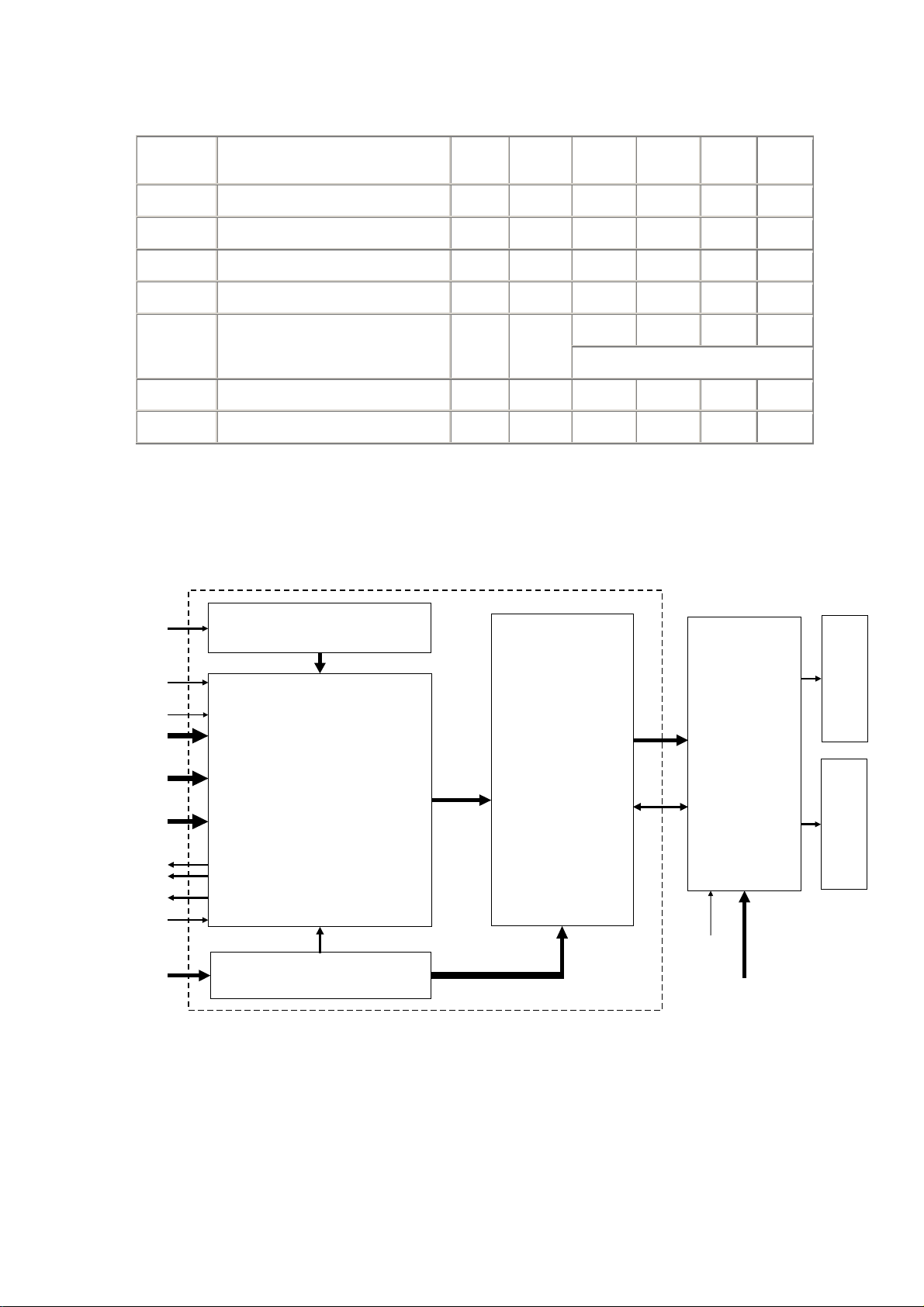
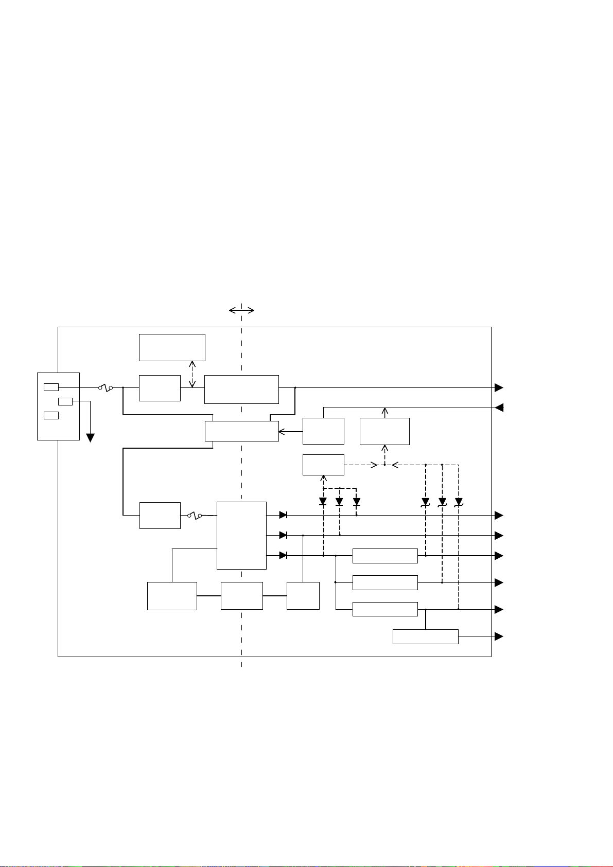
4.1. AVC Block Diagram
AV Controller
CVBS/
YC-out
Local keys (6)
Front AV in
(CVBS+Y/C, L/R)
Head Phone in
(CVBS+RGB, L/R)
(CVBS+RGB, L/R)
Phono
Line Out (L/R)
Power supply
SCART101
(TV out)
SCART102
(Monitor out)
SCART100
(Monitor out)
Y/C Out
CVBS Out
(fixed level)
RF input
for AVC
100-240V
(CVBS+Y/C, L/R, AV Link)
Y/C plug
Front Panel Board
10-WAY
AVC MAIN Board
Control items
Picture
Comb
Sound
Headphone Volume/Balance
OSD/TELETEXT
Advanced OSD
(this OSD cannot be
displayed in PC mode)
19-WAY
Power Supply Board
50-WAY
FC4 Board
Control items
Picture (at FC)
Colour saturation
Tint (hue)
Black stretch
Noise reduction
Wide format
Brightness
PC related
Simple OSD
(for use with PC)
7-WAY AND 9-WAY
CTI
LTI
OSD
DVI-24
DIN 8
PDP Monitor
Control items
Picture
Contrast
White Balance
Sound
Volume
Balance
Bass
Treble
Spatial effect
TruBass
I/Rin
Power supply
for PDP display
100~240V
SPEAKER
Common
SPEAKER
Common
4.2.
Tuner/Video Chroma (Schematic Sheet 1)
VHF/UHF asymmetric type tuner converts RF input signal to IF signal output through pin 11. AGC voltage
is supplied at pin 1 from IC100 pin 62. IF output goes through buffer Q101 to SAW filter SAW100 for VIF at
pin 2 and 3 of IC100 and to SAW101 for SIF at pin 63 and 64.
2
AV3000 AVC Unit Service Manual
Page 7
CRN Type Description Remarks
UV1316/A
TUN100
SAW100 K3953M SAW filter
SAW101 K9456M SAW filter Sound carrier 40.40MHz for standard L
IC100 TDA9321H
TR100 TPWA01B Nominal centre freq. Fn1=6.0MHz and Fn2=6.5MHz
TR101 TPWA04B Nominal centre freq. Fn1=5.5MHz and Fn2=5.742MHz
X100 Crystal 3.58MHz
X101 Crystal 4.43MHz
1G-3
313914716781
Asymmetric type tuner
Video Chroma and
Video switch
Supply voltage: +5V at pin 7 and +33V at pin 9
Control by I
Picture carrier 33.90MHz, picture to sound carrier
distance 6.5MHz for standard L
Supply voltage : +8V at pin 11 and 48 (AS)
Control by I
2
C, SDA at pin 5 and SCL at pin 4.
2
C, SDA at pin 47 and SCL at pin 46
4.2.1. IF Demodulator and Video Chroma
Demodulated video signal is output from pin 10 going to sound traps. There are two sound traps,
TR100 for I/L signal and TR101 for BG, outputs from which are switched by SOUND-SWITCH from
IC301 pin 5.
After group delay correction at pin 13, it is connected to pin 14 where TV picture is supplied into video
switch. The TV signal from pin13 is also connected to SCART1 as TV signal output.
Quasi Split Sound converted from SIF input is output at pin 5 to connect with sound decoder IC301.
H and V sync pulses are output at pin 60 and 61 to go to FC/MSC for Synchronisation to convert
progressive scan. H pulse must be inverted by Q126.
When selecting one of video signal in video switch of IC100, CVBS signal is going to COMB filter if the
video is CVBS PAL/NTSC format. Then Y/C separated signal is coming back at pin 28 and 29. The
clock must be provided from pin 30. The video or Y/C signal selected pass through video chroma
section and finally converted to YUV format at pin 49, 50, 51. IC100 is supplied 4.43MHz and 3.58MHz
clock from crystal X100 and X101, which is automatically selected according to the signal received. 2
RGB inputs are also switched at the last stage in IC100. RGB signals are also converted to YUV.
Video Switch.
AV3000 AVC Unit Service Manual
3
Page 8
Pin
No.
14 Input TV signal input
16 Input CVBS - SCT100-TOP (AV2) input
18 Input CVBS - SCT100-BOTTOM (AV3) input
20 Input CVBS/Y - SCT101 (AV1) input
21 Input C - SCT101 (AV1) input
23 Input CVBS/Y - front AV (FRONT) input
24 Input C - front AV (FRONT) input
28 Input Y - from COMB filter
29 Input C - from COMB filter
15 Input SCT100-TOP (AV2) pin 8 detection
17 Control SCT100-BOTTOM (AV3) pin 8 detection
- Control SCT101 (AV1) pin 8 detection is done by micro IC704 pin 28
Description
26 Output Go to COMB filter and phono video output
32 Output Go to micro for TELETEXT decoding
34 Output Go to SCT100-TOP (AV2) and SCT100-BOTTOM (AV3) as monitor video output
20 Output L/L' switch for SAW filter in/out at SAW101
22 Control Micro sw to switch SVHS or CVBS for front AV input
4.3. Sound/AV3 Control (Schematic Sheet 2)
4.3.1. NICAM/A2 Decoder and Sound Control
QSS signal is coming from IC100 to pin 58 through amplifier Q308/Q307. The signal level at pin 58
should be 0.1~0.8V
p-p
.
Sound output L/R at pin 28 and 29 are connected through amplifier Q310/Q312 for L and Q309/Q311
for R to adjust 500mVrms at PL700 pin 4 and 6 in the condition of AV sound input 500mVrms, FM
modulation 54%.
Sound output L/R at pin 28 and 29 are also connected through IC300 TDA7433 and IC303 to
headphone. Monitor sound L/R outputs for speaker are connected headphone and phone out. IC300
contributes separate volume control.
Headphone sound L/R controlled its level by IC300 are amplified.
AV3000 AVC Unit Service Manual
4
Page 9
CRN
Type
Description Remarks
IC301 MSP3410
X300 Crystal 18.432MHz
IC300 TDA7433 Basic audio processor
IC303 TDA2822D Headphone sound amplifier Supply voltage: +6.5V at pin 2
PL300 Connector for front control PCB
IC302
(OPTION)
TDA8440 Future option. Not used for this model.
NICAM/A2 sound decoder and audio
switch
Supply voltage: +5V at pin 18 and pin 51
Control by I
pin 9
Supply voltage: +8V at pin 17
Control by I2C, SDA at pin 19 and SCL at
pin 18
2
C, SDA at pin 10 and SCL at
4.3.2. Audio Switch
Pin
No.
52 Input SCT101 (AV1) sound L input
53 Input SCT101 (AV1) sound R input
49 Input SCT100-TOP (AV2) sound L input
Description
50 Input SCT100-TOP (AV2) sound R input
46 Input SCT100-BOTTOM (AV3) sound L input
47 Input SCT100-BOTTOM (AV3) sound R input
43 Input front AV (FRONT) sound L input
44 Input front AV (FRONT) sound R input
55 Input mono sound input from IC100
37 Output SCT101 (AV1) sound L output
36 Output SCT101 (AV1) sound R output
34 Output SCT100-TOP (AV2) / SCART3 (AV3) sound L output
33 Output SCT100-TOP (AV2) / SCART3 (AV3) sound R output
29 Output Speaker / Headphone/phone sound L output
28 Output Speaker / Headphone/phone sound R output
Output
5
Control
SOUND SWITCH for trap of TV input signal
AV3000 AVC Unit Service Manual
5
Page 10

4.3.3.
TDA7433
Basic Audio Processor (IC300)
Pin
No.
6 Input Audio sound L input
5 Input Audio sound R input
16 Output Phono sound L output
15 Output Phono sound R output
14 Output Headphone sound L output
13 Output Headphone sound R output
Description
4.3.4. Front AV Video Switch
PL300 is the connector for the front control PCB.
At pin 12 of PL700, CVBS from AV3 is connected.
At pin 11 of PL700, Y from AV3SVHS is connected.
At pin 9 indication of SVHS connector insertion is supplied to micro IC704 pin 38 and then it controls
micro-sw from pin 22 of IC100 in order to select Y from pin 11 of PL700 (micro-sw=H) or to select
CVBS from pin 12 of PL700 (micro-sw=L).
At pin 15 of PL700, C from AV3SVHS is connected to pin 24 of IC100.
4.4.
Interface Board (Schematic Sheet 3)
For Component Input, Progressive Sync Separation and Centre Audio Channel.
Sync separation for progressive YPbPr input (50Hz and 60Hz) are carried out at TA1370. Input video
signal is specifically given from AV4 and connected at pin 26 through clamping circuit constituted by
QC25~QC28. Sync separation for all input signal other than Progressive input are carried out at
TDA9321 (page 1). TA1370 includes switch of sync signal (H and V) between H/V input (pin I and
pin2) from TDA9321 and internal sync separation. TA1370 outputs H at pin16 and V at pin 28, which
are connected to PSF for FC4 board. There are 2 inputs of the connector for each main and sub. H
output at pin 16 on TA1370 is fed to IC10 to shorten H pulse waveform to avoid jittering.
2 inputs, main YUV from IC03 and RGB from micro (TELETXT), are switched and connected to subvideo input for FC4 (IC107). This is enabled when TV+TEXT is selected (SUB TELETEXT) and when
PC window is selected (SUB VIDEO)
AV3000 AVC Unit Service Manual
6
Page 11
CRN Type Description
Remarks
Sync separation for
IC08 TA1370
Component (progressive)
input
Supply voltage: +9V at pin 11
Control by I
XC01 Crystal 50KHz
IC02/IC03 TA1287 YUV/RGB switch
IC04
Supply voltage: +9V at pin 16
Control by DC voltage at pins 9/10/11 and matrix at pin 16
Audio switch, main L/R or AV4 (components input)
L/R. main L/R comes from MSP3410 audio switch
Video switch, Front video or AV4 (in case of YCbCr
IC05
BU4066 Analogue switch
normal components), which is connected to
TDA9321 for sync separation
Audio switch, Centre sound or AV4 (components
IC06
input) L/R. Output goes to IC04 to switch another
audio input
IC07 BU4053
IC09 M62320FP I/O expanders
Analogue Switch for Subvideo
Supply voltage: +9V at pin 16
Supply voltage: +5V at pin 13
Control by I
4.4.1. TA1287
2
C, SDA at pin 21 and SCL at pin 22
2
C, SDA at pin 3 and SCL at pin 2
supply
voltage:
+9V at pin
14
YUV/RGB switch (IC02/IC03)
Input:
Output:
CRN Remarks
IC02 YUV: Main signal
IC03 YUV: from IC02
YUV: at pin 1/2/3, Y:1 V
(incl. sync), UV:0.3Vp-p
p-p
RGB: at pin 6/7/8, 0.7Vp-p
IC02 Connect to IC03
IC03 Connect to FC4 through buffers
YUV: at pin13/14/15, Y:1 V
IC02 0V: through Matrix control of RGB input:
IC03 Always 1.6V:RGB > YUV
(incl. sync), UV:0.3Vp-p
p-p
(YUV can also input.
In this case, matrix control should be through)
IC02 0V: external (Components input) Control:
IC03 0V: Video
AV3000 AVC Unit Service Manual
7
Page 12
4.4.2.
M62320FP
I/O expanders (IC09)
Pin
Pin
No.
4 D00 Component video IC02, IC05 Components input Other than components
5 D01 Matrix IC02 RGB --> YUV Through
6 D02 PC IC07 Not PC mode (SUB TEXT) PC mode (SUB video in PCW)
7 D03 OSD-blank IC03 Kill OSD OSD enabled
9 D04 Cinema IC06, IC04 Audio centre not selected Audio centre selected
10 D05 Clamp-source IC05 CP from TA1370 SC from TDA9321
11 D06 TV/TEXT IC03 TEXT (select RGB input) TV
12 D07 N.C.
Description Connect to L H
Name
4.5. Power Circuit/Level Shifter (Schematic Sheet 4)
Power Supply Connector PSP from Power Supply board:
Pin
No.
Pin
Name
Remarks
1 POWER1
2,3,4 N.C.
5 +5VSTB Stand-by 5V for micro controller circuit
6 GND
7,8 N.C.
9 GND
10 GND
11 +5.5V1 5.5V supply 1
12 GND
13 +9.5V1 9.5V supply 1
14 GND
15 +5.5V2 5.5V supply 2
16 GND
17 +9.5V2 9.5V supply2
Power ON/Stand-by control
H: ON, L: Stand-by
18 GND
19 FE+30V 30V supply for tuner
AV3000 AVC Unit Service Manual
8
Page 13
4.5.1.
Voltage Regulators
CRN Type
I603 BA06T
IC602 SI-3050LSA
IC603 SI-3050LSA
IC601 SI-3033LSA
Q602 TK11125M
IC604 BA09FP
Remarks
Input +9.5V2 - Output +8V
For video chroma circuit (page 1)
Input +5.5V1 - Output +5VFE
For tuner (page 1)
Input +5.5V2 - Output +5V
For audio processor circuit (page 2), comb filter (page 6)
Input +5VSTB - Output 3.3VSTB
For micro-controller circuit
Input +5VSTB - Output 2.5VSTB
For micro-controller circuit
Input +9.5V1 - Output +9V
For interface circuit (Sheet 3)
4.5.2. Level Shift for Control Buses
CRN Type
Q607 BSS138 3WB-DATA to change from 3V3 to 5V
Q603 2SC2412K 3WB-CLOCK to invert with 5V range
Remarks
Q604 2SC2412K FC-ENABLE to invert with 5V range
Q605 2SC2412K MSC-ENABLE to invert with 5V range
Q614 BSS138 1900TX to change from 3V3 to 5V
4.6. Micro-controller (Schematic Sheet 5)
SCL3v3 and SDA3v3 are converted for 5V operation in Q700, Q701, Q705 & Q706. OSD/TEXT RGB
at pin 58/59/60 are synchronised with progressive sync pulses 2H (32KHz) at pin 32 and V (50/60Hz)
at pin 33. RGB and BLK are also converted to 5V operation at Q713, Q714, Q715 and IC707. AV link
is bi-directional bus from pin 10 of SCT101 made by Q709/D701~D703. For the micro, input and
output are separated. The signal level is also converted between 3V3 in micro and 5V for SCART.
See 'Micro-controller Pinout' in the PINOUT DATA section of this manual for microcontroller pin functions.
(IC701B Option not fitted.)
CRN Type Description Remarks
IC704 SDA5550 Micro-controller See below
X700 Crystal 6MHz
IC700 M24C16W EEPROM (16k-bits)
Supply voltage: +3.3VSTB at pin 8
Control by I
at pin 6 and WC3v3 at pin 7
2
C: SDA3v3 at pin 5 and SCL3v3
IC701 AT49LV002N
K6T1008V2E-GB70000 or
IC703
equivalent
IC705 M62703SL/ML Reset IC for IC704 Supply voltage: +3.3VSTB at pin 1
Flash memory (256Kbytes) for
software stored
SRAM, SMT (128kbytes)
Supply voltage: +3.3VSTB at pin 32
Control by address and data buses
Supply voltage: +3.3VSTB at pin 32
Control by address and data buses
9
AV3000 AVC Unit Service Manual
Page 14
4.6.1.
SDA5550
Micro-controller (IC704)
Supply voltage: +3.3VSTB at pin 8, 40, 75 and 92 and +2.5VSTB at pin 6, 22, 56 and 73.
Control through I
2
C: SDA3v3 at pin 52 and SCL3v3 at pin 47.
3 wire bus: 3WB-clock3v3 at pin 41 and 3WB-data3v3 at pin 46:
• FC-enable at pin 42
• MSC-enable at pin 43
• OSD enable at pin 44
Control through/by AVlink: output at pin 16 and input at pin 33.
RS232C (19200bps): TxD3v3 at pin 32 and RxD3v3 at pin 38.
Control by I/R in: at pin 34.
4.6.2.
Front Panel Board Connector
PL702
Pin
Pin
No.
Name
1 POW LED I Power LED
2 POWER SAVE I POWER2
3 STB+5V I Stand-by 5V power supply
4 GND - GND
5 RM-IN O N.C.
6 A+5V I +5V
7 A/D KEY 2 O Key in 1
8 A/D KEY 1 O Key in 2
9 (BS-LED) - N.C.
10 (MODEM-LED) -
In/Out Functions
At Front Control
N.C.
4.7. COMB Filter/SVHS Output (Schematic Sheet 6)
CVBS from IC100 pin 26 is filtered by C800, C801, L800, and C802 and connected to pin 3.
Y/C separate signals output from IC101 pin 25/23 are also filtered by Q801 base circuit and Q802
base circuit.
• Y is amplified to adjust the level at Q119/Q120 for return signal to IC100 and SVHS. Y signal
output via buffer Q803.
• C is amplified to adjust the level at Q121/Q122 for return signal to IC100 and SVHS. C signal
output via buffer Q804.
IC101 requires clock at pin 19 supplied from IC100.
4.7.1.
TC9090AF
COMB filter (IC101)
Supply voltage: +5V at pin 15, 18 and 27.
Control by I
2
C: SDA at pin 8 and SCL at pin 9.
10
AV3000 AVC Unit Service Manual
Page 15
4.7.2.
SVHS Output Connector
SVHS100
Pin
Functions
No.
1,2 GND 4 Y
3 C 5 GND (SW)
Pin
No.
Functions
4.8. SCART/FC-MSC Connection (Schematic Sheet 7)
4.8.1. SCART Connectors
Pin
No.
1 Sound o/p R Sound o/p R Sound o/p R
2 Sound i/p R Sound i/p R Sound input R
3 Sound o/p L Sound o/p L Sound o/p L
4 GND GND GND Audio common retu rn
5 GND GND GND Blue return
6 Sound i/p L Sound i/p L Sound i/p L
7 N.C. Blue-in Blue-in
8 Switch Switch Switch
9 GND GND GND Green return
10 AVLINK N.C. N.C. AVlink: TTL level
AV1
SCT101
AV2
SCT100-TOP
AV3
SCT100-BOTTOM
General Specification
Audio output R: ≤1KΩ, nominal 0.5Vrms ±3dB, max
2Vrms: 54% modulation in FM/AM
Audio input R: ≥10KΩ, nominal 0.5Vrms, min.0.2Vrms,
max 2Vrms
Audio output L: ≤1KΩ, nominal 0.5Vrms 3dB, max
2Vrms: 54% modulation in FM/AM
Audio input L: ≥10KΩ, nominal 0.5Vrms, min.0.2Vrms,
max 2Vrms
Blue: 75Ω, 0.7 ±0.1V
Function switch: ≥10KΩ, ≤2nF, Level 0: 0~2V, Level
1A: +4.5~7V (16:9), Level 1B: +9.5~12V (4:3)
11 N.C. Green-in Green-in
12 N.C. N.C. N.C. Under consideration
13 GND GND GND Red return
14 GND GND GND Blanking return
15 C in Red-in Red-in
16 N.C. Fast Blanking Fast Blanking
17 GND GND GND Video output return
18 GND GND GND Video input return
19 TV output Monitor o/p Monitor output
20 CVBS/Y in CVBS in CVBS in
21 GND GND GND Common return and contact 8, 10, 12
Green: 75Ω, 0.7 ±0.1V
Red/C: 75Ω, 0.7 ±0.1V (Red), ±3dB at 1 V
(C)
Blanking: 75Ω, logical 0 (off): 0~0.4V, logical 1: +1~3V
Video/Y output: 75Ω, 1 V
+10dB)
Video input: 75Ω, 1 V
p-p
±3dB (sync 0.3V -3dB +10dB)
p-p
11
AV3000 AVC Unit Service Manual
Y signal
p-p
±3dB (sync 0.3V -3dB
Page 16
4.8.2.
26-way Connector
Connection with FC/MSC Board (PL700).
Assuming that 1
V
video signal with 75 ohm terminated is input through SCT100-BOTTOM (AV3):
p-p
• UV are inverted by Q609, Q612, Q610 & Q613 to CbCr (U'V') at pin 25/24 and those are
adjusted to the level at 1.4Vp-p
5. AVC POWER BOARD DESCRIPTIONV T
AC INLET
AC in
100~240V
• Y is amplified by Q608/Q611 to adjust the level at 1.4V for signal and 0.6V for sync (2V
total) at pin 26
Sound level L and R at pins 6/4 should be 500mVrms on the condition that:
• 500mVrms audio is input through SCT100-BOTTOM (AV3)
• BG FM sound with 54% modulation is received
Connection with FC/MSC Board (PL701).
5.1. AVC Power Board Block Diagram
Primary
Secondary
Over-voltage
Protection
Circuit
Fuse F901
4A/250V
To Frame
GND
R914, Q902~4
Standby
Rectifier
D902
Main
Rectifier
D901
Switching
Regulator
Fuse F902
2A/250V
I901
Standby
DC/DC
Converter
Relay
Switching
Transformer
T901
Photo-
coupler
I902
H901
S901
(Detect
Voltage-down)
Error
Amp
Driver
Q934,
D938
Relay
SW
Q930
Q932
16V
Protection
Circuit
DC/DC Converter
I931, D950, L931
DC/DC Converter
I933, D949, L932
DC/DC Converter
I930, D959, L933
Q931, Q933
DC/DC Converter
(Detect
Voltage-over)
I932
in
p-p
STBY +5V
to AV Board
POWER on/off
from AV Board
30V
to AV Board
9.5V
to AV Board
1.8V
to FC Unit
3.3V
to AV Board/FC Unit
5.5V
to AV Board/FC Unit
5V
to FC Unit
5.2.
Switching Regulator, Controller and Power MOS FET
STR-F6668B (I901).
Supply voltage at pin 4:
• Over +16V (start operating),
• over +10V (keep operating).
AV3000 AVC Unit Service Manual
12
Page 17
Pin
Description
No.
1 Feedback input
2 Source of power MOS FET
3 Drain of power MOS FET
4 Power supply input for controller
5 GND
5.3. DC+5V Switching Regulator Module
uPM0518SA (H901).
Supply voltage: DC +120~375V at pin 1.
Pin
No.
Description
1 DC (+) voltage input
Inputs
Outputs
5 DC (-) voltage input
7 Feedback input 1
8 Feedback input 2
6 DC (-) voltage output
9 DC (+) voltage output
5.4. Photo-coupler
TLP621 (I902).
5.5.
Switching Regulators
SPI-8010A (I930).
Supply voltage: DC +8.5~50V at pin 11.
Pin
No.
Inputs
Output 7 Switching output
Description
11 DC voltage input
15 Feedback input
SI-8010GL (I931).
Supply voltage: DC +8~50V at pin 5.
Pin
No.
Inputs
Output 4 Switching output
Description
5 DC voltage input
8 Feedback input
2 Output ON/OFF
AV3000 AVC Unit Service Manual
13
Page 18

SI-8033JD (I933).
Supply voltage: DC +5.3~40V at pin 1.
Pin
No.
Description
1 DC voltage input
Inputs
Output 2 Switching output
4 Feedback input
5 Output ON/OFF
5.6. DC+5V Series Regulator
SI-3050LSA (I932).
Supply voltage: DC +5.1~8V at pin 1 & 3.
Pin
No.
Inputs
Outputs
Description
1 DC voltage input
3 DC voltage input
7 DC +5V output
8 DC +5V output
5.7. Connectors
PSP connector for AV Board.
PFP1 connector for FC4 unit.
PFP2 connector for FC4 unit.
AV3000 AVC Unit Service Manual
14
Page 19

6. FC4 BOARD DESCRIPTION
6.1. FC4 Board Block Diagram
PC input
FH12-50S-0.5PH
MCb
MCr
SCr
SCb
DATA
CLK
FC-ENA
OSD-CS
OSD-DATA
OSD-CLK
K_DET
32C-PDP(TXD)
32C-PDP(RXD)
AVDET
Remo-PDP
PMRST
PDDET
KMASK
GND
MY
MH
MV
SY
SH
SV
From
AV Board
FA+5.5V
FSTB+5V
GND
From
POWER
Unit
D+1.8V
D+3.3V
GND
DSUB-15
5 4 3 2 1
10
9 8 7 6
15 14 13 12 11
DDC
24LC221A
STB+5V
L
R
ZH-7
ZH-9
G/B/R
H,V
Buff
Buff
Buff
MSEPSW
REG
Buff
SSEPSW
Buff
R
TVH,V
PSAVE
RGB
MY
Buff
MCLPY1/2
MCLPCB1/2
MCLPCR1/2
MCLAMPW
R
AI+5S
A+5.5V
AI+5M
A+5V
AI+5S
STB+5V
D+1.8V
D+3.3V
M61303FP
clamp
RGB SW
adjust contrast
clamp
synchronous
separation
synchronous
SW
TA1358F
clamp
synchronous
separation
synchronous
SW
A+5V
RGB
SCL, SDA
adjust black-level
TV/PC
PCCLMP
MCLAMPW
AI+5M
Y/Cb/Cr
TA1358F
TVH,V
MSYNCSW
SSYNCSW
DATA/C LK/ EN/ODATA
OCLK/OENA/K_DET
STB+5V
TV/RBG
SW
PI5C3390
SCLPY1/2
SCLPCB1/2
SCLPCR1/2
SCLAMPW
SVW
STB+5V
MYI/MCBI/MCRI
H1,V1
VPOL,HPOL
VDET,HDET
TV/PC
5V>3.3V
STB+5V
synchronous
separation
STB+5V
synchronous
SW
SW_DLY
MWH
MWV
ZF14
A+5V REG
WFILSW1/2
A+5V REG
SFILSW1/2
A+5.5V
TL2932
micro-computer
A+5V REG
5V>3.3V
A+5V REG
SCL,SDA
ICS1523MT
A+5V REG
REG
5V>3.3V
EXT
SPLL
3.3V>5V
EEPROM
M24C08
‚w‚n
D+3.3V
STB+5V
H8-2238
LOOPFIL SW
EXT
MPLL
LOOPFIL SW
TC7SH32FU
SN74HCT1G32
Xtal
WPLLCLK
SS
MYI/MCBI/MCRI
MAVDY/CB/CR
MDVDY/CB/CR
MVRHY/CB/CR
MVRLY/CB/CR
SVRHY/CB/CR
SVRLY/CB/CR
SAVDY/CB/CR
SDVDY/CB/CR
MHW,VW
MAVD
PLL
MCPO
MHWATN
MVMASKW
MHVARIW
MCLKW
SAVD
PLL
SCPO
SYI/CbI/CrI
SHW,VW
SCLKW
SVMASKW
SHVARIW
SPLLINH
XOCLK
KMASK
A/D
A/D
DLY
XRST
16MSDRAM
MSM56V16160F
Control SDRAM
convert I/P
input matrix
scaling reduction
Main
Control W
Sub
MB87M1300
microcomputer I/F
EXTLD
CPUCLK
XCPUEN
PBLK
3.3V
RR
R R
DATADIR
D+3.3V
SDRAS
SDAD
SDIOXYZ
LCTI
scaling expansion
FC4
PBGA352
CPUDATA
STB+5VD+3.3V
5V 3.3V
b-directional buffer
SN74LVCC3245APW
x3
SDCLK
SDWE
SDCAS
color management
gamma correct/dither
Control R
to each block
VSS
RESET IC
PST-
3642NR
STB+5V
insert OSD
VDDH
D+3.3V
D+1.8V
SDAVD
PLL
insert blanking
RESET
DY OUT
DCB OUT
DCR OUT
DACLK
PDYS
VD
HD
POE
VDDL
D+1.8V
STB+5V
HRST
D+3.3V
R
D+3.3V
HDCP
KEY
EEPROM
TMDS
SiT168CT64
5V 3.3V
HSCL
HSDA
TXD
RXD
STB+5V
D+3.3V
T‚w0/1/2/C
PARITY
STB+5V
RS-232C
DS14C232CM
AVDET/PMRST/L/R
Remo-PDP/PDDET
ZH-8
TXD
RXD
DIN-8
GND
TXD
RXD
Software
RES
+5V
Writer
FEW
MD2
FCK
To
monitor
8
16
24
7
15
23222120191817
6
14
5
13
4
12
3
11
2
10
9
AVDET
8
7 6
5
4 3
2 1
1
DVI-24
15
AV3000 AVC Unit Service Manual
Page 20

7. PINOUT DATA
7.1. Micro-controller Pinout (SDA5550)
Digital Monolithic IC (IC704)
Note *:
Power key input:
ON Stand-by
H(1.5V) L H(1.2V)
H(1.0V) L L
H(1.5V) H(1.5V) H(1.5V)
Power
Save
Pin
No.
9 0.0 POWER-ON IN Power key input *
10 0.1 POWER1 OUT Power control 1
11 0.2 POWER2 OUT Power control 2
12 0.3 (I) POWER-LED5V OUT Power LED control
13 0.4 (I) OSD-RESET OUT PC OSD reset
14 0.5 (I) PM-RESET OUT PDP reset
15 0.6 WC#EEPROM OUT EEPROM enable
Port
No.
Port0
Function
Inverted (I) or Buffered (B)
Function
In/Out Notes
16
41 1.0 3WB-CLOCK (I) 3WB-CLOCK5V OUT 3 wire bus clock
42 1.1 FC-ENABLE (I) FC-ENABLE5V OUT FC enable
43 1.2 MSC-ENABLE (I) MSC-ENABLE5V OUT MSC enable
44 1.3 (I) OSD-EN OUT PC OSD enable
Port1
45 1.4 (I) MSP-RESET OUT MSP3410 reset
46 1.5 3WB-DATA (B) 3WB-DATA IN/OUT 3 wire buses data
47 1.6 SCL-3V3 (B) SCL OUT I2C bus clock
52
24 2.0 ADC0 FROM SCART1 PIN 8 IN Scart 101 (AV1) pin8 detect
25 2.1 ADC1 FROM TUNER AGC IN AGC level detect
Port2
26 2.2 PDDET FROM PDP IN PDP ON detect
27
0.7 AV-LINK-OUT (I) AVLINK OUT AV link output
1.7 SDA-3V3 (B) SDA IN/OUT I2C bus data
2.3 ADC3 FROM FRONT SWITCHES IN Vol&Prog. key input
16
AV3000 AVC Unit Service Manual
Page 21

31 3.0 IF TRAP ADJACENT CHANNELS OUT Not used
32 3.1 1900TX-3v3 OUT
33 3.2 SCI FROM AVLINK IN AV link input
34 3.3 IR1 IR FROM PDP IN IR input
Port3
35 3.4
36 3.5 MAP1 A18 ON SRAM OUT SRAM mapping
37 3.6 MAP2 A15/A18 SWITCH OUT SRAM mapping
38
48 4.2 MEM RD# OUT SRAM output enable
Port4
49
FRONT-SVHSSOCKET
3.7 1900RX IN
4.3 MEM WR# OUT SRAM write enable
IN S-VHS socket detect
PDP communication via
RS232C
PDP communication via
RS232C
7.2.
AVC-PDP Connectors
7.2.1. DVI74320-4004
24-way Digital Interface Cable Connector (P301P)
PIN
No:
AVC
(FC4)
PDP
PIN
No:
AVC
(FC4)
PDP
1 TX2- > TX2- 13 N.C. - N.C.
2 TX2+ > TX2+ 14 +5VAVDET > +5VAVDET
3 SHIELD - SHIELD 15 GND - GND
4 N.C. - N.C. 16 HPDET > HPDET
5 N.C. - N.C. 17 TXD- > TXD6 SCLH > SCLH 18 TXD+ > TXD+
7 SDAH > SDAH 19 SHIELD - SHIELD
8 N.C. - N.C. 20 N.C. - N.C.
9 TX1- > TX1- 21 N.C. - N.C.
10 TX1+ > TX1+ 22 SHIELD - SHIELD
11 SHIELD - SHIELD 23 TXC+ > TXC+
12 N.C. - N.C. 24 TXC- > TXC-
AV3000 AVC Unit Service Manual
17
Page 22

7.2.2.
TC57587-01-401
8-way Digital Interface Cable Connector (P302P)
PIN
No:
1 TXD > TXD
2 RXD < RXD
3 PARITY > PARITY
4 REMO-PDP < REMO-PDP
5 AUDIO L > AUDIO L
6 AUDIO R > AUDIO R
7 PDDET < PDDET
8 AVDET2 > AVDET2
AVC
(FC4)
PDP
7.3.
FC4 Connectors
7.3.1. FPC Connector
FH12-50S-0.5SV 0.5mm pitch (PSF)
Pin
No.
1 GND GND I/O I2C bus DATA
2 N.C. N.C. I/O I2C bus CLOCK
3 GND GND - GND
4 DATA DATA I/O 3-wire DATA 5V CMOS
5 CLK CLK I 3-wire CLOCK 5V CMOS
6 GND GND - GND
7 FC-ENA FC-ENA I FC micro enable 5V CMOS
8 MSC-ENA OSD-CS I MSC micro enable 5V CMOS
9 DATA OSD-DATA I 3-wire DATA 5V CMOS
AVC
PSF
Pin Name
FC4
P001
Pin Name
In/
Out
Function Notes
10 CLK OSD-CLK I 3-wire CLOCK 5V CMOS
11 GND GND - GND
12 N.C. N.C.(2H) O 2H sync for OSD
13 N.C. K_DET I Enable for OSD generator
14 N.C. N.C.(2V) O 2V sync for OSD
15 N.C. KMASK I RESET for OSD generator
16 GND GND - GND
18
AV3000 AVC Unit Service Manual
Page 23

17 RS232C-PDP(TxD) 32C-PDP (TXD) I RS232C-TxD 5V CMOS
18 RS232C-PDP(RxD) 32C-PDP (RXD) O RS232C-RxD 5V CMOS
19 GND GND - GND
20 +5VSTB AVDET I PDP control
21 N.C. N.C. I MATRIX control
22 Remo-PDP Remo-PDP O R/C command from PDP 5 V CMOS
23 GND N.C. - GND
24 PM RST PM RST I PDP control 5V CMOS
25 PD DET PD DET O PDP control 5V CMOS
26 GND GND - GND
27 MY MY I Video Y 1.4V±0.06Vp-p
28 MCb MCb I Video Cb 0.7v±0.03Vp-p
29 MCr MCr I Video Cr 0.7v±0.03Vp-p
30 GND GND - GND
31 MH MH I Main H sync 5V CMO S
32 MV MV I Main V sync 5V CMOS
33 GND GND - GND
34 SY SY I Sub Y/G
35 SCb SCb I Sub Cb/B 0.7 ±0.03Vp-p
36 SCr SCr I Sub Cr/R 0.7 ±0.03Vp-p
37 GND GND - GND
38 SH SH I Sub H sync 5V CMOS
39 SV SV I Sub V sync 5V CMOS
40 GND GND - GND
41 GND GND (OSD/TXT G) I GND
42 GND GND (OSD/TXT B) I GND
43 GND GND (OSD/TXT R) I GND
44 GND GND (OSD BLK/Ys) I GND
1.4 ±0.06Vp-p (Y) /
0.7 ±0.03Vp-p (G)
45 GND GND (OSD/Ym) I GND
46 GND GND - GND
47 AUDIO L AUDIO L I Audio L Typ 500mVrms
48 GND GND - GND
49 AUDIO R AUDIO R I Audio R Typ 500mVrms
50 GND GND - GND
19
AV3000 AVC Unit Service Manual
Page 24

7.3.2.
7-P Connector
Base SM3 1.5mm Pitch (PFP1)
Pin
No.
FC4
P002P
Pin Name
In/Out Function Notes
1 FA+6.0V I 6V power supply
2 FA+6.0V I 6V power supply
3 GND - GND
4 GND - GND
5 FSTB+5V I Stand-by +5V 50mA
6 FSTB+5V I Stand-by +5V
7 GND - GND
7.3.3. 9-P Connector
Base SM3 1.5mm Pitch (PFP2)
Pin
No.
FC4
P003P
Pin Name
1 D+1.8V I 1.8V power supply 500mA
2 D+1.8V I 1.8V power supply
3 GND - GND
In/Out Function Notes
460m
A
4 GND - GND
5 D+3.3V I 3.3V power supply 350mA
6 D+3.3V I 3.3V power supply
7 D+3.3V I 3.3V power supply
8 GND - GND
9 GND - GND
AV3000 AVC Unit Service Manual
20
Page 25

8. SERVICING INFORMATION
8.1. Diagnostics
Phenomenon
PDP LED is
flashing
No picture See "AV Board Troubleshooting"
Picture unstable
Noisy picture on
RF (TV)
No sound
No WSS
response and no
TELETEXT
50-way cable between AVC and FC4? Cable disconnected
Digital interface cable DVI24 or DIN8 disconnected? Cable disconnected
Crystal oscillates?
Comb filter works?
VIF inputs around pins 1~4 of IC100 input proper signal?
Slow response toward R/C handset R319 disconnected
IC301 pins 58/59 input proper signal (0.1~0.8Vp-p) F-sound-out line component failure
IC100 pin 32 signal observed?
Check
Point
Potential
Problem
Dry joint/solder bridge
X100/C135/X101/C136
Component dry joint/solder
bridge/broken in CHROMA lines,
e.g. R208/Q121/Q122
Components of comb clock IC101 pin
19
Dry joint/solder bridge at pins 1~4 or
broke device of IC100
Pin 32 solder bridge (to pin 31)/dry joint
or in line of CVBS-micro
8.2.
No picture,
power working
Composite,
component in
No Picture
Both
RF, video
All
No picture
Pins 49~51
of IC100?
AV Board Troubleshooting
Component IN only
No picture
RF
in
Check TR101 & TR100
No
Pin 10 of
IC100?
Check IC100
& around
Yes
Pins 1~4
of IC003, signal
observed?
Yes
No
Check IC02
& parts around
Check SAW
No
filter, tuner
& around
Pins 16 & 28
of IC08?
Yes
Check pins 1,
No
2, 21, 22 & 26
of IC08
Check IC10
between
IC03 & PSF
Yes
AV3000 AVC Unit Service Manual
21
Page 26
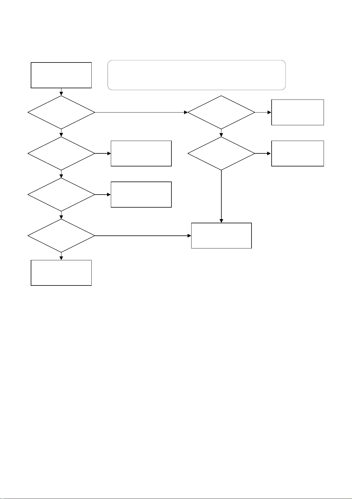
8.3.
No picture,
no sound
Power Board Troubleshooting
Caution!
Always confirm that C907 (CE220uF/450V) is discharged prior to
touching the POWER Board with fingers or soldering iron after
power-off to prevent electric shock and secondary damage.
LED is
dark?
Yes
Fuse F901
is OK?
Yes
C931 (+)
voltage ~
5.2V?
Yes
Q933 (G)
voltage >
1.0V?
Yes
Operation of
protection
circuit
No
No
No
No
Check D901,
D902, etc.
Check D902,
R914, H901, etc.
LED is
lit in
green?
Yes
Relay
S901 is
ON?
Yes
Main switching
regulator
problem
No
Check
AV Board
No
Check
S901
AV3000 AVC Unit Service Manual
22
Page 27
8.4.
Service Menu Data
CYAN
background means to separate data for each 32/37/42".
RED figures are new default values.
1st 2nd 3rd 4th 5th
TUN>
SVC>
(*1)
PC >
ADC
OPT
AGC
BIF
LIF
AFC
PC1 >
PC2>
GSW
BLP
COP
MBC
MCC 5D 5D 5D
32"
Values
HEX
READ READ READ AGC data
80 80 80 Option for destination
ADJ ADJ ADJ AGC adjustment
ADJ ADJ ADJ AFC adjustment for all except L'
ADJ ADJ ADJ AFC adjustment for L'
READ READ READ AFC level indication
01 01 01 Gamma switch PDP 10 D3:D2
7F 7F 7F Black Level RGB; user brightness control for PC FC4 5 D07:D00
7F 7F 7F Contrast (RGB) FC4 6 D07:D00
7F 7F 7F Main brightness centre FC4 7 D15:D08
37"
Values
HEX
42"
Values
HEX
Functions
Main contrast centre FC4 7 D07:D00
MXB
BGP
CCP
DCP
PC3> PSE
6C 6C 6C Brightness Max. for wide NORMAL/REAL FC4 7 D15:D08
00 00 00 Brightness/Gradation PDP 27&28 D2&D2
00 00 00 NTSC/EBU PDP 27&28 D1&D1
01 01 01 Tracking correction PDP 27&28 D0&D0
01 01 01 PC power save enable/disable FC4 4 D08
23
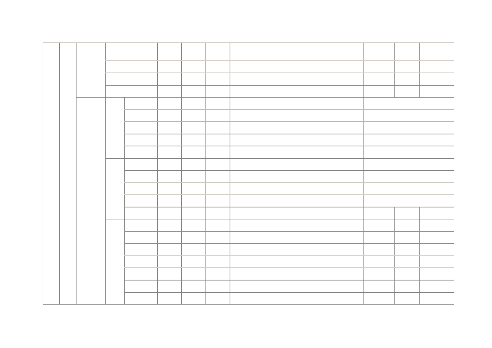
AV3000 AVC Unit Service Manual
Page 28

PST
0F 0F 0F Power save timer
SIG>
FLA
MAX
MIN
SNR
MIS> RGB>
COL>
NOM>
WAM>
R1
G1
B1
R2
G2
B2
R3
OK OK OK
READ READ READ Max signal level on screen
READ READ READ Min signal level on screen
READ READ READ FC noise level indication
READ READ READ Gain R; warm
READ READ READ Gain G; warm
READ READ READ Gain B; warm
READ READ READ Gain R; normal
READ READ READ Gain G; normal
READ READ READ Gain B; normal
READ READ READ Gain R; cool
CAUTION!! Never press OK unless proper signal is
displayed, auto signal level adjustment activates.
PDP
Read/Write
PDP
Read/Write
PDP
Read/Write
PDP
Read/Write
PDP
Read/Write
PDP
Read/Write
PDP
Read/Write
13/20
13/21
13/22
12/17
12/18
12/19
11/14
1st D7:D0 /
D7:D0
2nd D7:D0 /
D7:D0
3rd D7:D0 /
D7:D0
1st D7:D0 /
D7:D0
2nd D7:D0 /
D7:D0
3rd D7:D0 /
D7:D0
1st D7:D0 /
D7:D0
GSW
G3
B3
READ READ READ Gain G; cool
READ READ READ Gain B; cool
01 01 01 Gamma switch PDP 10 D3:D2
PDP
Read/Write
PDP
Read/Write
11/15
11/16
2nd D7:D0 /
D7:D0
3rd D7:D0 /
D7:D0
24
AV3000 AVC Unit Service Manual
Page 29
WHB
00 00 00
White balance 0;cool, 1;normal, 2;warm --synchronising with user operation MENU
PDP 9
D3:D2&D1:D
0
MI0>
HAPC
BRN
APC
M01>
M02>
M03>
(*2)
F01(4:3)
F02(16:9)
F03(C16:9L)
F04(T16:9L)
F05(14:9)
F06(C14:9L)
F07(T14:9L)
F08(PAN)
F09(14:9LS)
PCA
HE1
HE2
01 01 01 Q.MODE + Heat APC PDP 28 D4:D3
01 01 01 Burn in mode PDP 10 D5:D4
00 00 00 APC switch 0;High APC, 1;Normal PDP 10 D7
01 01 01 Wide mode selected by 16:9 key (0;on, 1;off) 4:3
00 00 00 Wide mode selected by 16:9 key (0;on, 1;off) WIDE SCREEN
00 00 00 Wide mode selected by 16:9 key (0;on, 1;off) LETTERBOX
01 01 01 Wide mode selected by 16:9 key (0;on, 1;off) T16:9L
01 01 01 Wide mode selected by 16:9 key (0;on, 1;off) 14:9
00 00 00 Wide mode selected by 16:9 key (0;on, 1;off) C14:9L
01 01 01 Wide mode selected by 16:9 key (0;on, 1;off) T14:9L
01 01 01 Wide mode selected by 16:9 key (0;on, 1;off) PANORAMIC
00 00 00 Wide mode selected by 16:9 key (0;on, 1;off) 14:9 ZOOM
02 02 02 PC wide mode 0;NORMAL, 1;REAL, 2;FULL FC4 3 D17:D16
02 02 02 Horizontal enhancer DYNAMIC FC4 2 D20:D19
03 03 03 Horizontal enhancer DYNAMIC-VIDEO FC4 2 D20:D19
HE3
HE4
HE5
HE6
HET
00 00 00 Horizontal enhancer NATURAL FC4 2 D20:D19
00 00 00 Horizontal enhancer NATURAL-VIDEO FC4 2 D20:D19
01 01 01 Horizontal enhancer CINEMA FC4 2 D20:D19
02 02 02 Horizontal enhancer CINEMA-VIDEO FC4 2 D20:D19
00 00 00 Horizontal enhancer TEXT FC4 2 D20:D19
25
AV3000 AVC Unit Service Manual
Page 30
M04>
(*2)
VE1
VE2
03 03 03 Vertical enhancer DYNAMIC FC4 2 D22:D21
03 03 03 Vertical enhancer DYNAMIC-VIDEO FC4 2 D22:D21
M05>
M06>
VE3
VE4
VE5
VE6
VET
BGT
CCT
TCR
DCC
WBC
BSO
SPC
PHC
PHU
03 03 03 Vertical enhancer NATURAL FC4 2 D22:D21
03 03 03 Vertical enhancer NATURAL-VIDEO FC4 2 D22:D21
03 03 03 Vertical enhancer CINEMA FC4 2 D22:D21
03 03 03 Vertical enhancer CINEMA-VIDEO FC4 2 D22:D21
00 00 00 Vertical enhancer TEXT FC4 2 D22:D21
00 00 00 Brightness/Gradation PDP 27&28 D2&D2
00 00 00 NTSC/EBU PDP 27&28 D1&D1
01 01 01 Tracking correction W/B Warm & Norm PDP 27&28 D0&D0
00 00 00 Tracking correction W/B Cool PDP 27&28 D0&D0
00 00 00
1F 1F 1F Black Stretch gain offset ON&MID FC4 7 D21:D16
00 00 00 PinP(PC W) picture contrast offset FC4 7 D07:D00
80 80 80 Colour phase centre FC4 8 D07:D00
1A 1A 1A PAL HUE offset (not available if AV2 is RGB) FC4 8 D07:D00
NHU
YU6
YU5
THU
YHU
20 20 20 NTSC HUE offset FC4 8 D07:D00
1D 1D 1D YCbCr / YPbPr @ 60Hz HUE offset FC4 8 D07:D00
1A 1A 1A YCbCr / YPbPr @ 50Hz HUE offset FC4 8 D07:D00
1F 1F 1F TEXT HUE offset FC4 8 D07:D00
1F 1F 1F Components Hue for Asian option FC4 8 D07:D00
26
AV3000 AVC Unit Service Manual
Page 31
FPB
00 00 00 FAVOURITE Peak Brightness 0;Peak, 1:Normal PDP 10 D6
MI1>
M11>
M12>
(*3)
BLT
MBC
MBX
COT
MCC
MCX
SAC
SAX
CE1
CE2
CE3
CE4
CE5
CE6
7F 7F 7F Black level (RGB) FC4 5 D07:D00
80 80 80
80 80 80 Brightness centre TEXT FC4 7 D15:D08
7F 7F 7F Contrast (RGB) FC4 6 D07:D00
89 89 89 Main contrast centre FC4 7 D07:D00
70 70 70 Contrast centre TEXT FC4 7 D07:D00
40 40 40 Saturation centre NTSC/PAL/RGB/YCbCr TV FC4 8 D14:D08
50 50 50 Saturation centre TEXT FC4 8 D14:D08
1F 1F 1F C-Vert/Horiz enhancer gain DYNAMIC-TV FC4 2 D12:D08
10 10 10 C-Vert/Horiz enhancer gain DYNAMIC-VIDEO FC4 2 D12:D08
1F 1F 1F C-Vert/Horiz enhancer gain NATURAL-TV FC4 2 D12:D08
10 10 10 C-Vert/Horiz enhancer gain NATURAL-VIDEO FC4 2 D12:D08
1F 1F 1F C-Vert/Horiz enhancer gain CINEMA-TV FC4 2 D12:D08
10 10 10 C-Vert/Horiz enhancer gain CINEMA-VIDEO FC4 2 D12:D08
Main brightness centre: (50) is used in AUTO
adjustment
FC4 7 D15:D08
M13>
CET
YET
YE1
YE2
YE3
YE4
10 10 10 C-Vert/Horiz enhancer gain TEXT FC4 2 D12:D08
00 00 00 Sharpness centre - TEXT FC4 2 D04:D00
1F 1F 1F Sharpness DYNAMIC-TV FC4 2 D04:D00
12 12 12 Sharpness DYNAMICT-VIDEO FC4 2 D04:D00
12 12 12 Sharpness NATURAL-TV FC4 2 D04:D00
12 12 12 Sharpness NATURAL-VIDEO FC4 2 D04:D00
27
AV3000 AVC Unit Service Manual
Page 32

YE5
12 12 12 Sharpness CINEMA-TV FC4 2 D04:D00
M14>
(*4)
M15>
(*5)
YE6
YE7
YE8
YI1
YI2
YI3
YI4
YI5
YI6
YIT
CI1
CI2
CI3
CI4
12 12 12 Sharpness CINEMA-VIDEO FC4 2 D04:D00
12 12 12 Sharpness centre-FAVOURITE-TV FC4 2 D04:D00
12 12 12 Sharpness centre-FAVOURITE-VIDEO FC4 2 D04:D00
01 01 01 YNR input gain DYNAMIC FC4 2 D07:D05
01 01 01 YNR input gain DYNAMIC-VIDEO FC4 2 D07:D05
01 01 01 YNR input gain NATURAL FC4 2 D07:D05
01 01 01 YNR input gain NATURAL-VIDEO FC4 2 D07:D05
01 01 01 YNR input gain CINEMA FC4 2 D07:D05
01 01 01 YNR input gain CINEMA-VIDEO FC4 2 D07:D05
01 01 01 YNR input gain TEXT FC4 2 D07:D05
00 00 00 CNR input gain DYNAMIC FC4 2 D15:D13
00 00 00 CNR input gain DYNAMIC-VIDEO FC4 2 D15:D13
00 00 00 CNR input gain NATURAL FC4 2 D15:D13
00 00 00 CNR input gain NATURAL-VIDEO FC4 2 D15:D13
M16>
CI5
CI6
CIT
OSH
OSV
OTH
00 00 00 CNR input gain CINEMA FC4 2 D15:D13
00 00 00 CNR input gain CINEMA-VIDEO FC4 2 D15:D13
00 00 00 CNR input gain TEXT FC4 2 D15:D13
109 109 109 H position - OSD
40 40 40 V position - OSD
190 190 190 H position - TEXT
28
AV3000 AVC Unit Service Manual
Page 33

OTV
40 40 40 V position - TEXT
MI2>
(*6)
M21>
M22>
SUR
CMB
DCN
DBR
DCL
DPB
DCM
DBS
DWB
DFT
NCN
NBR
NCL
NPB
00 00 00 SURROUND ON:1, OFF:0
01 01 01 COMB FILTER ON;1, OFF;0
3E 3E 3E DYNAMIC Contrast
80 80 80 DYNAMIC Brightness
50 50 50 DYNAMIC Colour
00 00 00 DYNAMIC Peak Brightness 0;Peak, 1:Normal PDP 10 D6
02 02 02 DYNAMIC Contrast Mode NORM;0, AUTO;1, DYN;2
1F 1F 1F DYNAMIC Black stretch 0;off, 01~3F; level
00 00 00 DYNAMIC White Balance 0:cool, 1;normal, 2;warm
01 01 01 DYNAMIC Film Mode 0;on, 1;off
38 38 38 NATURAL Contrast
80 80 80 NATURAL Brightness
48 48 48 NATURAL Colour
00 00 00 NATURAL Peak Brightness 0;Peak, 1:Normal PDP 10 D6
M23>
NCM
NBS
NWB
NFT
TCN
TBR
01 01 01 NATURAL Contrast Mode NORM;0, AUTO;1, DYN;2
1A 1A 1A NATURAL Black stretch 0;off, 01~3F; level
00 00 00 NATURAL White Balance 0:cool, 1;normal, 2;warm
01 01 01 NATURAL Film Mode 0;on, 1;off
3E 3E 3E CINEMA Contrast
80 80 80 CINEMA Brightness
29
AV3000 AVC Unit Service Manual
Page 34

TCL
50 50 50 CINEMA Colour
MI3>
(*7)
M24>
M31>
TPB
TCM
TBS
TWB
TFT
DGS
NGS
TGS
PGS
DPM
NPM
TPM
PPM
MVB
MTR
00 00 00 CINEMA Peak Brightness 0;Peak, 1:Normal PDP 10 D6
00 00 00 CINEMA Contrast Mode NORM;0, AUTO;1, DYN;2
1F 1F 1F CINEMA Black stretch 0;off, 01~3F; level
01 01 01 CINEMA White Balance 0:cool, 1;normal, 2;warm
00 00 00 CINEMA Film Mode 0;on, 1;off
01 01 01 DYNAMIC Gamma Select
01 01 01 NATURAL Gamma Select
01 01 01 CINEMA Gamma Select
02 02 02 PERSONAL Gamma Select
00 00 00 DYNAMIC Picture Mode
01 01 01 NATURAL Picture Mode
01 01 01 CINEMA Picture Mode
02 02 02 PERSONAL Picture Mode
0B 0B 0B MUSIC Volume Balance
0B 0B 0B MUSIC Treble
M32>
MBA
MTB
MMS
NVB
NTR
0B 0B 0B MUSIC Bass
03 03 03 MUSIC TruBass 0;off, 1;low, 2;mid, 3;high
01 01 01 MUSIC Matrix Surround 0;off, 1;on
0B 0B 0B SPEECH Volume Balance
10 10 10 SPEECH Treble
30
AV3000 AVC Unit Service Manual
Page 35

NBA
0B 0B 0B SPEECH Bass
MI4>
(*8)
M33>
M41>
M42>
NTB
NMS
TVB
TTR
TBA
TTB
TMS
TSW
TC1
TC2
TC3
TC4
ABS
NLA
00 00 00 SPEECH TruBass 0;off, 1;low, 2;mid, 3;high
00 00 00 SPEECH Matrix Surround 0;off, 1;on
0B 0B 0B CINEMA Volume Balance
10 10 10 CINEMA Treble
10 10 10 CINEMA Bass
02 02 02 CINEMA TruBass 0;off, 1;low, 2;mid, 3;high
01 01 01 CINEMA Matrix Surround 0;off, 1;on
00 00 00 TDA9178 fitted or not. 0:not fitted, 1;fitted
01 01 01 TDA9178 address 00 TDA9178 00 D07:D00
10 10 10 TDA9178 address 01 TDA9178 01 D05:D00
00 00 00 TDA9178 address 02 TDA9178 02 D07:D00
00 00 00 TDA9178 address 03 TDA9178 03 D05:D00
00 00 00 TDA9178 address 04 TDA9178 04 D05:D00
00 00 00 TDA9178 address 05 TDA9178 05 D05:D00
M43>
VGM
PKG
STP
CRG
LWD
1RD
20 20 20 TDA9178 address 06 TDA9178 06 D05:D00
00 00 00 TDA9178 address 07 TDA9178 07 D05:D00
00 00 00 TDA9178 address 08 TDA9178 08 D05:D00
00 00 00 TDA9178 address 09 TDA9178 09 D05:D00
00 00 00 TDA9178 address 0A TDA9178 0A D05:D00
14 14 14 White balance offset 1; R_DRIVE MAX
31
AV3000 AVC Unit Service Manual
Page 36

(*9)
1GD
0F 0F 0F White balance offset 1; G_DRIVE
M44>
M45>
1BD
1RG
1GG
1BG
2RD
2GD
2BD
2RG
2GG
2BG
3RD
3GD
3BD
3RG
00 00 00 White balance offset 1; B_DRIVE
1F 1F 1F White balance offset 1; R_GAMMA
1F 1F 1F White balance offset 1; G_GAMMA
1F 1F 1F White balance offset 2; B_GAMMA
00 00 00 White balance offset 2; R_DRIVE CENTRE
00 00 00 White balance offset 2; G_DRIVE
00 00 00 White balance offset 2; B_DRIVE
1F 1F 1F White balance offset 2; R_GAMMA
1F 1F 1F White balance offset 2; G_GAMMA
1F 1F 1F White balance offset 2; B_GAMMA
00 00 00 White balance offset 3; R_DRIVE MIN
0F 0F 0F White balance offset 3; G_DRIVE
29 29 29 White balance offset 3; B_DRIVE
1F 1F 1F White balance offset 3; R_GAMMA
MI5> M51>
(*10)
3GG
3BG
CEA
CEB
CEC
CED
1F 1F 1F White balance offset 3; G_GAMMA
1F 1F 1F White balance offset 3; B_GAMMA
0D 0D 0D C-Vert/Horiz enhancer gain DYNAMIC-RGB/YCbCr
0D 0D 0D C-Vert/Horiz enhancer gain DYNAMIC-YPbPr
0D 0D 0D C-Vert/Horiz enhancer gain NATURAL-RGB/YCbCr
0D 0D 0D C-Vert/Horiz enhancer gain NATURAL-YPbPr
32
AV3000 AVC Unit Service Manual
Page 37

CEE
0D 0D 0D C-Vert/Horiz enhancer gain CINEMA-RGB/YCbCr
M52>
M53>
CEF
CEM
YEA
YEB
YEC
YED
YEE
YEF
YE9
YE0
LC1
LC2
LC3
LC4
0D 0D 0D C-Vert/Horiz enhancer gain CINEMA-YPbPr
10 10 10 CTI MID level in menu (FAVOURUTE)
10 10 10 Sharpness DYNAMIC-RGB/YCbCr
10 10 10 Sharpness DYNAMIC-YPbPr
08 08 08 Sharpness NATURAL-RGB/YCbCr
02 02 02 Sharpness NATURAL-YPbPr
10 10 10 Sharpness CINEMA-RGB/YCbCr
10 10 10 Sharpness DYNAMIC-YPbPr
10 10 10 Sharpness centre on FAVOURITE-RGB/YCbCr
10 10 10 Sharpness centre on FAVOURITE-YPbPr
1F 1F 1F Favourite + TV; last CTI
10 10 10 Favourite + Video; last CTI
0D 0D 0D Favourite + RGB/YCbCr; last CTI
0D 0D 0D Favourite + YPbPr; last CTI
M54>
DCV 50 50 50
NCV 3E 3E 3E
TCV
SAV 3E 3E 3E
DCO
NCO
40 40 40 CINEMA + VIDEO/RGB; colour
58 58 58 DYNAMIC + YCbCr/YPbPr; colour
4B 4B 4B NATURAL + YCbCr/YPbPr; colour
DYNAMIC + VIDEO/RGB; colour
NATURAL + VIDEO/RGB; colour
FAVOURITE + VIDEO/RGB; colour
33
AV3000 AVC Unit Service Manual
Page 38

TCO
50 50 50 CINEMA + YCbCr/YPbPr; colour
OPT>
HOT>
OB0
OB1
EMG
AV DELAY
RGB Comb
FC4
ASIAN
OPTIONS>
OPT
SAO
AV2
INITIAL INSTALL
COUNTRY SELECT
LANGUAGE
SELECT
TELETEXT
44 44 44 FAVOURITE + YCbCr/YPbPr; colour
78 78 78 Option byte 1
80 80 80 Option byte 2
0 0 0 0:Normal, 1:Macrovision improved
OFF OFF OFF
OFF OFF OFF
RGB RGB RGB RGB or YUV
ON ON ON INITIAL INSTALL menu is on or off
ON ON ON Country select is on or off
ON ON ON European language select is on or off
ON ON ON TELETEXT is working or not
0 0 0 Hotel option
ON;Go through Comb, OFF;skip Comb It is affected to
SVC>MIS>MI1>M11=HP2/4
Enters FC4 sub menu
VRS>
VOL
PRG
MN
MSU
PDU
PWT
CENTRE CENTRE CENTRE Maximum volume limited in Hotel mode
1 1 1 Start up position number
READ READ READ Model name
READ READ READ MSU micro version number
READ READ READ PDP micro version number
READ READ READ PDP working hour
34
AV3000 AVC Unit Service Manual
Page 39

E2>
E2R
OK OK OK EEPROM reset
E2F
E2S
E24
EXS
OK OK OK EEPROM factory setting
OK OK OK EEPROM is set to the shipment
OK OK OK EEPROM in FC4 is initialised
OK OK OK Escape from service menu
Notes:
(*1): Maximum of 8 items on one page.
(*2): LTI picture mode.
(*3): CTI picture mode.
(*4): YNR picture mode.
(*5): CNR picture mode.
(*6): [ ]; Menu related value is decimal, it is ok to display in hex. E.g. [32] is centre of CONTRAST, [63] is MAX for CONTRAST.
(*7): [ ]; Menu related value is decimal, it is ok to display in hex. E.g. [11] is centre of BALANCE, [21] is MAX for TREBLE.
(*8): TDA9178 option. Values are fixed in this menu. No individual parameter on TC1~TC4 can be set.
(*9): WB Offset OFF/1/2/3 option.
(*10): Add 27 bytes.
35
AV3000 AVC Unit Service Manual
Page 40
9. UNIT WIRING DIAGRAM
9.1. AVC Unit
POWER Board
EFP1
EFP2
PFP2
PSC
Note:
Before fixing the CONTROL Board,
PSC connector should be inserted
nto the board
PFP1
CONTROL Board
Lead clamp for EFP1, EFP2,
ESC and EARTH should be locked
after fixing EARTH and looped
EFP1, EFP2 and ESC wires
ESC
PSP
EFP1, EFP2, ESC and
EARTH should never
be bunched together
with ZSC (Nittoh
adhesive tape
No. 188
L=50mm)
P001P
ESF
PSF
P002P
EFP1
EFP2
P003P
PSP
EARTH
ESC
Terminals of EARTH wire should be fixed with
two screws, one for the POWER Board and the
other for the front key
Preparation:
EARTH wire should be wrapped
& soldered with two 1P-terminals
10 10
150
AV Board
ESC
PL702
Lead clamp for EFP1, EFP2 and ESC
should be locked after fixing EFP1
and EFP2 and looped wires
Note:
Make sure the loop is held down
so that it is not pinched by the
top cover
Specification
1. This Drawing shows the wire dressing and connection of
the AVC3-E Final Assembly.
2. Connectors with wire should be inserted into plug pin
posts as shown on the table below:
Connectors with wire
Name
Assembly list Board
ESC FINAL Assembly CONTROL Brd PSC AV Board PL702
EFP1 FINAL Assembly POWER Board PFP1 HCP111 P002P
EFP2 FINAL Assembly POWER Board PFP2 HCP111 P003P
ESF FINAL Assembly AV Board PSF HCP111 P001
PSP POWER Board AV Board PSP - -
3. For plug pin posts with lock function, connector housings
should be inserted deep enough so that it can be locked.
4. For plug pin posts without lock function, connector housings
should be inserted as deeply as possible.
5. Flexible flat cable ESF should be fixed as shown on the
drawing below:
HCP111
Insert into the
deepest position
and lock
Plug Pin 1 Plug Pin 2
Printing
side
Name
Board
ESF
Name
PSF
36
AV3000 AVC Unit Service Manual
Page 41

10. ASSEMBLY DIAGRAM
10.1. AVC Unit
Control Board
FC4PDP Board
(FC4 Unit)
Scrambling part in HDCP
Don't remove shield case
Power
Board
AV Board
37
AV3000 AVC Unit Service Manual
Page 42

11. SCHEMATIC DIAGRAMS
SM00033
AV3000 AVC Unit Service Manual
AV BOARD - Tuner/Video Chroma
38
Page 43

SM00033
AV3000 AVC Unit Service Manual
AV BOARD - Sound/AV3 Control
39
Page 44

SM00033
AV3000 AVC Unit Service Manual
AV BOARD - Interface Board
40
Page 45

SM00033
AV3000 AVC Unit Service Manual
AV BOARD - Power Circuit (Voltage Regulator)/Level Shifter
41
Page 46

SM00033
AV3000 AVC Unit Service Manual
AV BOARD - Micro-controller
42
Page 47

SM00033
AV3000 AVC Unit Service Manual
AV BOARD - COMB Filter/SVHS Output
43
Page 48

SM00033
AV3000 AVC Unit Service Manual
AV BOARD - SCART/FC-MSC Connection
44
Page 49

0. 2
4. 8
0
4.8
4. 8
Switching Reg. Module
33 5
0
33 5
0
0
33 4
0
5.3
0
-0 . 1
-0. 3
5.2
34. 6
5. 2
0
0
0
4. 4
0
4. 4
30. 8
to AV Board
3.3 V Reg .
0. 6
1.3
0
0
0
14 .8
Switching Reg.
0
3. 3
1. 8
0
17 .5
24
0
5. 0
5. 0
5. 0
17 .5
5. 5 3 . 3
23
17 .5
1. 7
5.5
0.9 7 . 6
0. 8
10. 0
14 .8
21
3. 5
Feed back
20
10 . 6
9.6
0. 8 0 . 8
5 . 5V Reg.
9. 6
6. 4
5. 8
17 .5
0
5. 5
0
FC 1 .8V R eg.
0
2. 2
3. 3
0
2. 2
0
0
3.3
to FC Unitu
to FC Unit
5. 6
SM00033
0
05 .6
5.6
5. 6
26
AV POWER BOARD
45
AV3000 AVC Unit Service Manual
5.5
5.5
0
0
FC STBY 5V Reg.
Page 50

SM00033
AV3000 AVC Unit Service Manual
CONTROL BOARD
46
Page 51

ACIN
FILTER Board
F902
AC NOISE FILTER
L
1
2
3
0. 47
H901
470K
1mH
2200pF
0. 47
2200pF
E1
(42V Only)
C902
0.47
AC250V
R902
3.3M
(42V Only)
L902
Z110
5mH
Z111
Z112
(42V Only)
Z113
AC250V
Z209
Z210
C903
0.47
(42V Only)
Z118Z119
Z211
L903
1mH
Z120Z121
(42V Only)
C906
0.47
AC250V
to POWER Unit
Z216
Z218
Z217
N
E902
Secondary
Ground
Mains Switch
COLD
32VGP1U281Q
42VGP1U281R
LED Board
to SIGNAL/SOUND Board
to SIGNAL/SOUND Board
SP Terminal
L Board
42V Only
COLD
to SIGNAL/SOUND Board
SM00033
AV3000 AVC Unit Service Manual
MAINS SWITCH, FILTER, SPEAKER L/R & LED BOARDS
47
SP Terminal
R Board
42V Only
COLD
Page 52

12. PCB LAYOUT DIAGRAMS
TOP (COMPONENT) SIDE
SM00033
AV3000 AVC Unit Service Manual
AV BOARD
48
Page 53

TOP (COMPONENT) SIDEBOTTOM (SOLDER) SIDE
SM00033
AV3000 AVC Unit Service Manual
POWER BOARD
49
Page 54

BOTTOM (SOLDER)
TOP (COMPONENT)
(R) BOARD
LED BOARD FOR 32V
SIDE
SIDE
(L) BOARD
SPEAKER TERMINAL
BOARD (42V ONLY)
LED BOARD FOR 42V
LED BOARD
CONTROL BOARD
FILTER BOARD
SM00033
AV3000 AVC Unit Service Manual
CONTROL, SPEAKER, LED & FILTER BOARDS
50
Page 55

THE UPDATED PARTS LIST
FOR THIS MODEL IS
AVAILABLE ON ESTA
Page 56

Hitachi, Ltd. Tokyo, Japan
International Sales Division
THE HITACHI ATAGO BUILDING,
No. 15 –12 Nishi Shinbashi, 2 – Chome,
Minato- Ku, Tokyo 105-8430, Japan.
Tel: 03 35022111
HITACHI EUROPE LTD,
Whitebrook Park
Lower Cookham Road
Maidenhead
Berkshire
SL6 8YA
UNITED KINGDOM
Tel: 01628 643000
Fax: 01628 643400
Email: consumer-service@hitachi-eu.com
HITACHI EUROPE GmbH
Munich Office
Dornacher Strasse 3
D-85622 Feldkirchen bei München
GERMANY
Tel: +49-89-991 80-0
Fax: +49-89-991 80-224
Hotline: +49-180-551 25 51 (12ct/min)
Email: HSE-DUS.service@hitachi-eu.com
HITACHI EUROPE srl
Via Tommaso Gulli N.39, 20147
Milano, Italia
ITALY
Tel: +39 02 487861
Tel: +39 02 38073415 Servizio Clienti
Fax: +39 02 48786381/2
Email: customerservice.italy@hitachi-eu.com
HITACHI EUROPE S.A.
364 Kifissias Ave. & 1, Delfon Str.
152 33 Chalandri
Athens
GREECE
Tel: 1-6837200
Fax: 1-6835964
Email: service.hellas@hitachi-eu.com
HITACHI EUROPE S.A.
Gran Via Carlos III, 86, planta 5
Edificios Trade - Torre Este
08028 Barcelona
SPAIN
Tel: 93 409 2550
Fax: 93 491 3513
Email: atencion.cliente@hitachi-eu.com
HITACHI Europe AB
Box 77 S-164 94 Kista
SWEDEN
Tel: +46 (0) 8 562 711 00
Fax: +46 (0) 8 562 711 13
Email: csgswe@hitachi-eu.com
HITACHI EUROPE S.A.S
Lyon Office
B.P. 45, 69671 BRON CEDEX
FRANCE
Tel: 04 72 14 29 70
Fax: 04 72 14 29 99
Email: france.consommateur@hitachi-eu.com
HITACH EUROPE AB
Egebækgård
Egebækvej 98
DK-2850 Nærum
DENMARK
Tel: +45 43 43 6050
Fax: +45 43 60 51
Email: csgnor@hitachi-eu.com
Hitachi Europe Ltd
Bergensesteenweg 421
1600 Sint-Pieters-Leeuw
BELGIUM
Tel: +32 2 363 99 01
Fax: +32 2 363 99 00
Email: sofie.van.bom@hitachi-eu.com
www.hitachidigitalmedia.com
HITACHI EUROPE LTD (Norway) AB
STRANDVEIEN 18
1366 Lysaker
NORWAY
Tel: 67 5190 30
Fax: 67 5190 32
Email: csgnor@hitachi-eu.com
HITACHI EUROPE AB
Neopoli / Niemenkatu 73
FIN-15140 Lahti
FINLAND
Tel : +358 3 8858 271
Fax: +358 3 8858 272
Email: csgnor@hitachi-eu.com
HITACHI EUROPE LTD
Na Sychrove 975/8
101 27 Pr aha 10 – Bohdalec
CZECH REPUBLIC
Tel: +420 267 212 383
Fax: +420 267 212 385
Email: csgnor@hitachi-eu.com
 Loading...