HIT HA17384HRP, HA17385HRP, HA17384SRP Datasheet

HA17384SPS/SRP, HA17384HPS/HRP,
HA17385HPS/HRP
High Speed Current Mode PWM Control IC
for Switching Power Supply
ADE-204-028A (Z)
2nd Edition
Nov. 1999
Description
The HA17384S/H and HA17385H are PWM control switching regulator IC series suitable for highspeed,
current-mode switching power supplies. With ICs from this series and a few external parts, a small, low
cost flyback-transformer switching power supply can be constructed, which facilitates good line regulation
by current mode control. Synchronous operation driven after an external signal can also be easily obtained
which offers various applications such as a power supply for monitors small multi-output power supply.
The IC series are composed of circuits required for a switching regulator IC. That is a under-voltage
lockout (UVL), a high precision reference voltage regulator (5.0 V ± 2%), a triangular wave oscillator for
timing generation, a high-gain error amplifier, and as totem pole output driver circuit which directly drives
the gate of power MOSFETs found in main switching devices. In addition, a pulse-by-pulse type, highspeed, current-detection comparator circuit with variable detection level is incorporated which is required
for current mode control.
The HA17384SPS includes the above basic function circuits. In addition to these basic functions, the H
Series incorporates thermal shut-down protection (TSD) and overvoltage protection (OVP) functions, for
configuration of switching power supplies that meet the demand for high safety levels.
Between the HA17384 and HA17385, only the UVL threshold voltages differ as shown in the product
lineup table.(See next page.)
This IC is pin compatible with the “3842 family” ICs made by other companies in the electronics industry.
However, due to the characteristics of linear ICs, it is not possible to achieve ICs that offer full
compatibility in every detail.
Therefore, when using one of these ICs to replace another manufacturer’s IC, it must be recognized that it
has different electrical characteristics, and it is necessary to confirm that there is no problem with the power
supply (mounting) set used.

HA17384SPS/SRP, HA17384HPS/HRP, HA17385HPS/HRP
Functions
• Under-voltage lockout system
• Reference voltage regulator of 5.0 V ± 2%
• Triangular wave (sawtooth) oscillator
• Error amplifier
• Totem pole output driver circuit (direct driving for power MOSFETs)
• Current-detection comparator circuit for current mode
• OVP function (over voltage protection) *
• TSD function (thermal shut-down protection) *
• Protect function by zener diode (between power input and GND)
Note: 1. H series only.
Features
• High-safety UVL circuit is used (Both VIN and Vref are monitored)
• High speed operation:
Current detection response time: 100 ns Typ
Maximum oscillation frequency: 500 kHz
• Low standby current: 170 µA Typ
• Wide range dead band time
(Discharge current of timing capacitance is constant 8.4 mA Typ)
• Able to drive power MOSFET directly
(Absolute maximum rating of output current is ±1 A peak)
• OVP function (over voltage protection) is included *
(Output stops when FB terminal voltage is 7.0 V Typ or higher)
• TSD function (thermal shut-down protection) is included *
(Output stops when the temperature is 160°C Typ or higher)
• Zener protection is included
(Clamp voltage between VIN and GND is 34 V Typ)
• Wide operating temperature range:
Operating temperature: –20°C to +105°C
Junction temperature: 150°C *
Note: 1. H series only.
2. S series only.
1
1
1
1
2
2

HA17384SPS/SRP, HA17384HPS/HRP, HA17385HPS/HRP
Product Line-up
UVL Power Supply
Package Additional Function
DILP8 (DP-8) SOP8 (FP-8DC)
TSD
(Thermal shutdown protection)
OVP
(Over voltage
protection) V
HA17384SPS HA17384SRP — — 16.0 10.0
HA17384HPS HA17384HRP ❍❍
HA17385HPS HA17385HRP ❍❍8.4 7.6
Pin Arrangement
Threshold Voltage
(V) Typ V
TH UVL
TL UVL
(V) Typ
COMP
FB
CS
R
T/CT
1
2
3
4
8
Vref
7
V
IN
6
OUT
GND
5
(Top view)
Pin Function
Pin No. Symbol Function Note
1 COMP Error amplifier output pin
2 FB Inverting input of error amp./OVP input pin 1
3 CS Current sensing signal input pin
4R
5 GND Groung pin
6 OUT PWM Pulse output pin
7VINPower supply voltage input pin
8 Vref Reference voltage 5V output pin
Note: 1. Overvoltage protection (OVP) input is usable only for the HA17384H and HA17385H.
/C
T
T
Timing resistance, timing capacitance connect pin
3

HA17384SPS/SRP, HA17384HPS/HRP, HA17385HPS/HRP
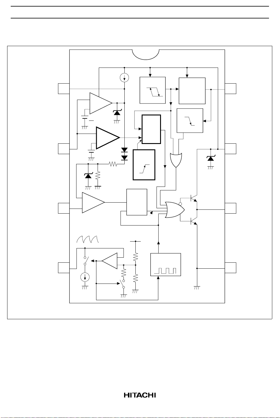
Block Diagram
COMP
FB
(OVP input)
CS
0.8mA
UVL1
1
−
EA
+
6.5V
1
Vref
2
(2.5V)
−
OVP
+
2
7.0V
1V
*1
2V
F
2R
R
−
CS
3
+
H
L
OVP
latch
S
TSD
sense
160°C
CS
latch
R
S
Q
PWM LOGIC
Vref
VL
VH
Q
5V band
gap
reference
regulator
UVL2
Vref > 4.7VR
OR
NOR
OUT
Totem pole
output circuit
34V
8
Vref
7
V
IN
6
OUT
RT/CT
Oscillator
4
8.4 mA
+
−
1.2V
2.8 V
Latch set
pulse
5 GND
Note: 1. Blocks with bold line are not included in HA17384SPS/SRP.
4

HA17384SPS/SRP, HA17384HPS/HRP, HA17385HPS/HRP
Absolute Maximum Ratings
Item Symbol Rating Unit Note
Supply voltage V
DC output current I
Peak output current I
Error amplifier input voltage V
COMP terminal input voltage V
Error output sink current I
Power dissipation P
IN
O
O PEAK
FB
COMP
OEA
T
Operating temperature Topr –20 to +105 °C
Junction temperature Tj 125 °C3
Storage temperature Tstg –55 to +125 °C3
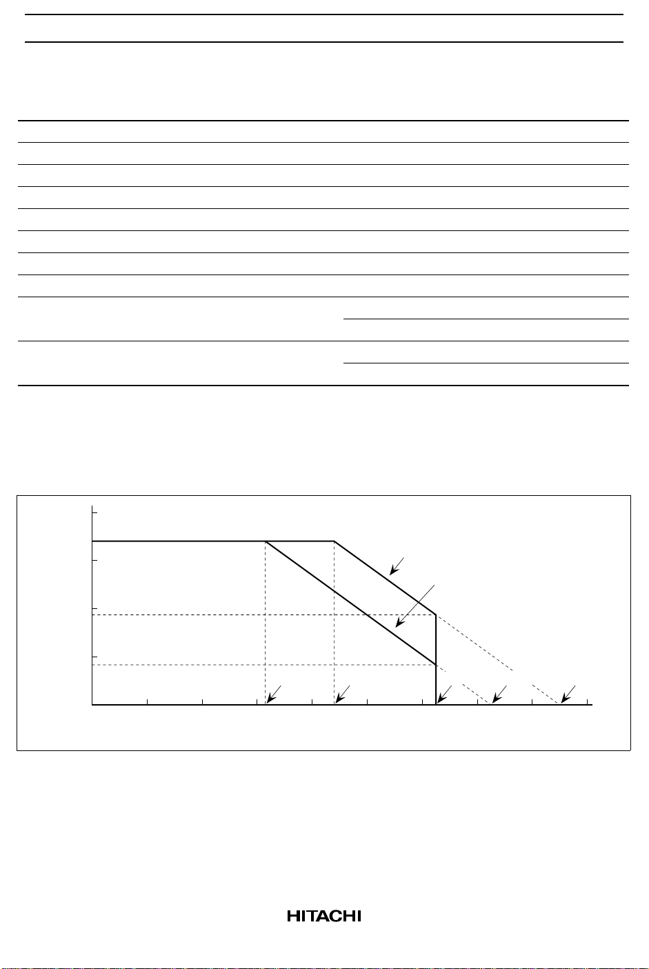
Notes: 1. For the HA17384HPS and HA17385HPS,
This value applies up to Ta = 43°C; at temperatures above this, 8.3 mW/°C derating should be
applied.
For the HA17384SPS,
This value applies up to Ta = 68°C; at temperatures above this, 8.3 mW/°C derating should be
applied.
30 V
±0.1 A
±1.0 A
–0.3 to V
IN
V
–0.3 to +7.5 V
10 mA
680 mW 1, 2
150 °C4
–55 to +150 °C4
800
680mW
600
(mW)
T
374mW
400
166mW
200
Power Dissipation P
43°C 68°C 150°C
HA17384SPS
HA17384HPS, HA17385HPS
105°C 125°C
0
−20 0 20 40 60 80 100 120 140 160
Ambient Temperature Ta (°C)
5

HA17384SPS/SRP, HA17384HPS/HRP, HA17385HPS/HRP
Absolute Maximum Ratings (cont)
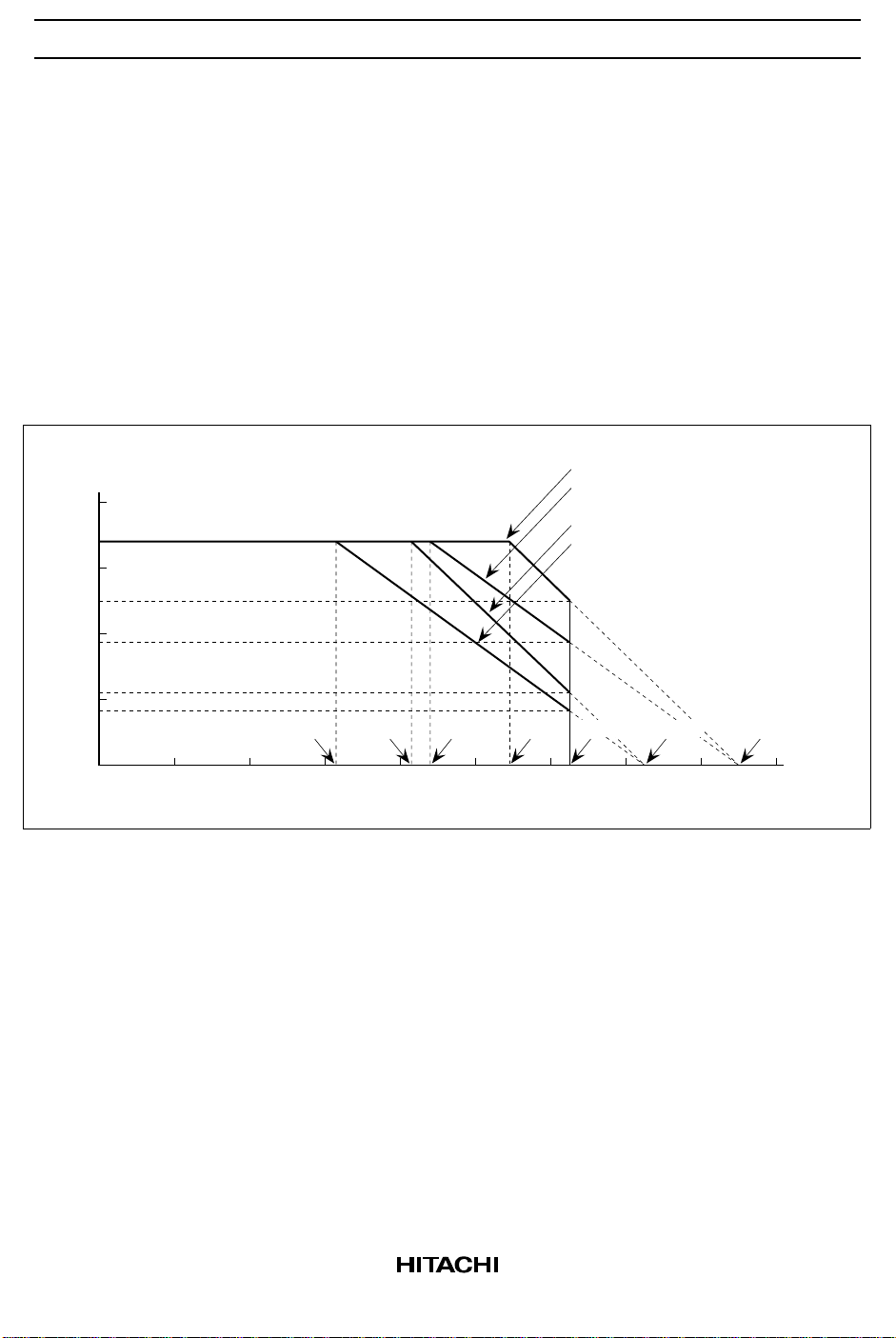
Notes: 2. This is the value when the device is mounted on a glass-epoxy substrate (40 mm × 40 mm × 1.6
mm). However,
For the HA17384HRP and HA17385HRP,
Derating should be performed with 8.3 mW/°C in the Ta ≥ 43°C range if the substrate wiring
density is 10%.
Derating should be performed with 11.1 mW/°C in the Ta ≥ 63°C range if the substrate wiring
density is 30%.
For the HA17384SRP,
Derating should be performed with 8.3 mW/°C in the Ta ≥ 68°C range if the substrate wiring
density is 10%.
Derating should be performed with 11.1 mW/°C in the Ta ≥ 89°C range if the substrate wiring
density is 10%.
HA17384SRP
: −11.1 mW/°C (wiring density is 30%)
800
600
(mW)
T
680 mW
500 mW
: −8.3 mW/°C (wiring density is 10%)
HA17384HRP, HA17385HRP
: −11.1 mW/°C (wiring density is 30%)
: −8.3 mW/°C (wiring density is 10%)
374 mW
400
222 mW
200
Power Dissipation P
166 mW
0
−20 0 20 40 60 80 100 120 140 160
3. Applies to the HA17384HPS/HRP and HA17385HPS/HRP.
4. Applies to the HA17384SPS/SRP.
43°C63°C
Ambient Temperature Ta (°C)
68°C 105°C 125°C
150°C89°C
6

HA17384SPS/SRP, HA17384HPS/HRP, HA17385HPS/HRP
Electrical Characteristics
(The condition is: Ta = 25°C, VIN = 15 V, CT = 3300 pF, RT = 10 kΩ without notice)
Reference Part
Item Symbol Min Typ Max Unit Test Condition Note
Reference output voltage Vref 4.9 5.0 5.1 V Io = 1 mA
Line regulation Regline — 20 50 mV 12 V ≤ V
Load regulation Regload — 10 25 mV –1 mA ≥ Io ≥ –20 mA
Output short current los –30 –100 –180 mA Vref = 0V
Temperature stability ∆Vref — 80 — ppm/°C Io = –1 mA,
–20°C ≤ Ta ≤ 105°C
Output noise voltage V
N
— 100 — µV 10 Hz ≤ fnoise ≤ 10 kHz 1
Notes: 1. Reference value for design.
Triangular Wave Oscillator Part
Item Symbol Min Typ Max Unit Test Condition Note
Typical oscillating frequency fosc Typ 47 52 57 kHz C
Maximum oscillating
frequency
Supply voltage dependency of
oscillating frequency
Temperature dependency of
oscillating frequency
Discharge current of C
T
Low level threshold voltage V
High level threshold voltage V
Triangular wave amplitude ∆V
Notes: 1. Reference value for design.
fosc Max 500 — — kHz
∆fosc 1 — ±0.5 ±2.0 % 12 V ≤ VIN ≤ 25 V
∆fosc 2 — ±5.0 — % –20°C ≤ Ta ≤ 105°C1
Isink
TLCT
THCT
CT
7.5 8.4 9.3 mA VCT = 2.0 V
CT
— 1.2 — V 1
— 2.8 — V 1
— 1.6 — V ∆VCT = V
IN
= 3300 pF,
T
R
= 10 kΩ
T
≤ 25 V
THCT
– V
TLCT
1
1
7

HA17384SPS/SRP, HA17384HPS/HRP, HA17385HPS/HRP
Electrical Characteristics (cont)
Error Amplifire Part / OVP Part
Item Symbol Min Typ Max Unit Test Condition Note
Non-inverting input voltage V
Input bias current I
Open loop voltage gain A
FB
IB
VOL
2.42 2.50 2.58 V V
— –0.2 –2.0 µAVFB = 5.0 V
65 90 — dB 2.0 V ≤ VO ≤ 4.0 V
Unity gain bank width BW 0.7 1.0 — MHz
Power supply voltage
PSRR 60 70 — dB 12 V ≤ VIN ≤ 25 V
rejection ratio
Output sink current I
Output source current I
High level output voltage V
Low level output voltage V
OVP latch threshold
Osink EA
Osource EA
OH EA
OL EA
V
OVP
3.0 9.0 — mA VFB = 2.7 V, V
–0.5 –0.8 — mA VFB = 2.3 V, V
5.5 6.5 7.5 V VFB = 2.3 V,
— 0.7 1.1 V VFB = 2.7 V,
6.0 7.0 8.0 V Increase FB terminal
voltage
OVP (FB) terminal input
I
FB(OVP)
—3050µAVFB = 8.0 V 1
current
OVP latch reset VIN voltage V
IN(OVP RES)
6.0 7.0 8.0 V Decreasing VIN after OVP
Note: 1. These values are not prescribe to the HA17384SPS/SRP because OVP function is not included.
= 2.5 V
COMP
R
= 15 kΩ(GND)
L
R
= 15 kΩ(Vref)
L
voltage
latched
COMP
COMP
= 1.1 V
= 5.0 V
1
1
8

HA17384SPS/SRP, HA17384HPS/HRP, HA17385HPS/HRP
Electrical Characteristics (cont)
Current Sensing Part
Item Symbol Min Typ Max Unit Test Condition Note
Voltage gain A
Maximum sensing voltage Vth
Power supply voltage
VCS
CS
PSRR — 70 — dB 12 V ≤ VIN ≤ 25 V 2
rejection ratio
Input bias current I
Current sensing
BCS
tpd 50 100 150 ns Time from when V
response time
Notes: 1. The gain this case is the ratio of error amplifier output change to the current-sensing threshold
voltage change.
2. Reference value for design.
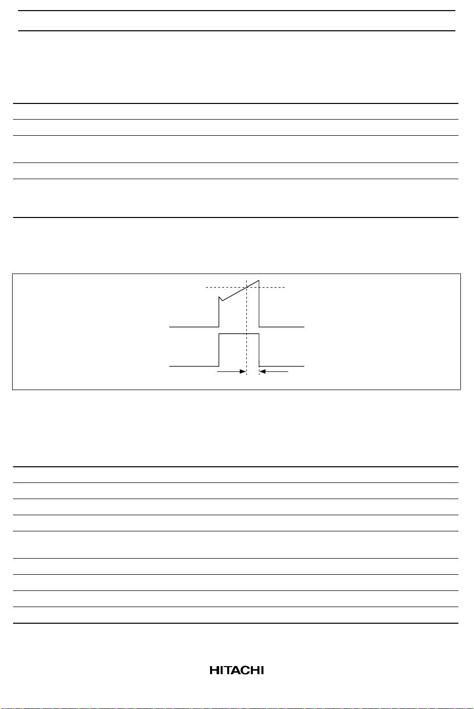
3. Current sensing response time tpd is definded a shown in the figure 1.
2.85 3.00 3.15 V/V VFB = 0 V 1
0.9 1.0 1.1 V
— –2 –10 µAVCS = 2 V
becomes 2 V to when
CS
output becomes “L” (2 V)
Vth
V
CS
3
V
OUT
(PWM)
tpd
Figure 1 Definition of Current Sensing Response Time tpd
PWM Output Part
Item Symbol Min Typ Max Unit Test Condition Note
Output low voltage 1 V
Output low voltage 2 V
Output high voltage 1 V
Output high voltage 2 V
Output low voltage at
V
OL1
OL2
OH1
OH2
OL STB
standby mode
Rise time t
Fall time t
r
f
Maximum ON duty Du max 94 96 100 %
Minimum ON duty Du min — — 0 %
Notes: 1. Pulse application test
— 0.7 1.5 V losink = 20 mA
— 1.5 2.2 V losink = 200 mA 1
13.0 13.5 — V losource = –20 mA
12.0 13.3 — V losource = –200 mA 1
— 0.8 1.1 V VIN = 5 V,
losink = 1 mA
— 80 150 ns CL = 1000 pF
— 70 130 ns CL = 1000 pF
9

HA17384SPS/SRP, HA17384HPS/HRP, HA17385HPS/HRP
Electrical Characteristics (cont)
UVL Part
Item Symbol Min Typ Max Unit Test Condition Note
Threshold voltage for V
TH UVL
high VIN level 7.6 8.4 9.2 V when VIN is rising 2
Threshold voltage for V
TL UVL
low VIN level 6.8 7.6 8.4 V voltage after turn-ON 2
V
UVL hysteresis voltage V
IN
Vref UVL threshold voltage V
HYS UVL
T Vref
Notes: 1. For the HA17384S/H.
2. For the HA17385H.
Total Characteristics
Item Symbol Min Typ Max Unit Test Condition Note
Operating current I
Standby current I
Current of latch I
Power supply zener
IN
STBY
LATCH
V
INZ
voltage
Overheat protection
Tj
TSD
starting temperature
Notes: 1. These values are not prescribe to the HA17384SPS/SRP because OVP function is not included.
2. V
= 8.5 V in case of the HA17384H.
IN
2. These values are not prescribe to the HA17384SPS/SRP because TSD function is not included.
4. Reference value for design.
7.0 10.0 13.0 mA CL = 1000 pF, VFB = VCS = 0 V
120 170 230 µA Current at start up
200 270 340 µAVFB = 0 V after VFB = V
31 34 37 V IIN + 2.5 mA
— 160 — °C 3, 4
14.5 16.0 17.5 V Turn-ON voltage 1
9.0 10.0 11.0 V Minimum operating 1
5.0 6.0 7.0 V V
HYS UVL
= V
TH UVL
– V
TL UVL
0.6 0.8 1.0 V 2
4.3 4.7 Vref V Voltage is forced toVref
terminal
OVP
1
1, 2
10
 Loading...