

HIT HA16666FP Datasheet

HA16666P/FP
600kHz PWM Controlled Switching Regulator
Description
The HA16666P/FP is a voltage mode PWM (pulse width modulation) control IC for switching regulator
control. It can drive a power MOS FET efficiently on 600 kHz. Its stanby current is 0.3 mA (max), and it is
used as the primary control power supply.
Functions
• +5 V reference voltage circuit
• Triangular waveform oscillator
• PWM comparator
• Output circuit (Totem pole output)
• Overcurrent protection circuit (with one-pulselatch mode)
• Undervoltage lockout protectoin circuit
• Soft start and quick shutdown function
• Remote control function
• Comparator with internal 1.3 V reference voltage
Features
• High-speed switching;
tr = 80 ns (15 V amplitude)
tf = 40 ns (15 V amplitude)
• Low power dissipation;
0.3 mA max in standby state
12 mA max in operation state (VIN = 15 V)
• Dual-slope highly accurate dead-band duty setup circuit; Setup accuracy Du = ±3% (max)
• Wide output pulse width control range; 0 to 75%

HA16666P/FP
• Undervoltage lockout protection;
VIN high threshold voltage 10 V typ
VIN low threshold voltage 8 V typ
• Two input threshold voltage for overcurrent protection cmparator;
fixed voltage (1.3 V)
variable voltage
• Double pulse output protection by overcurrent protection circuit with one-pulse latch mode
• Wide input supply voltage range; VCC = 11 to 40 V
Ordering Information
Type Package
HA16666P DP-16
HA16666FP FP-16DA
2
Pin Arrangement
HA16666P/FP
E/I
ST
C
R
T1
R
T2
OSC Out
GND
N.C
1
2
3
T
4
5
6
7
8
16
15
14
13
12
11
10
9
N.INV
–
INV
CS
Vref
V
IN
RM
OUT
N.C
+
(Top View)
Pin Functions
Pin No. Symbol Descreption
1 E/I Error input
2 ST Soft start
3C
T
4RT1Timing resistor (rise section)
5RT2Timing resistor (fall section)
6 OSC Out Triangular waveform oscillator
7 GND Ground
8 N.C No connect
9 N.C No connect
10 OUT Pulse output
11 RM Remote control
12 V
IN
13 Vref Reference voltage (5 V) output
14 CS Comparator input (–) with reference voltage (1.3 V)
15 INV
16 N.INV
–
+
Timing capacitance
Power supply voltage
Comparator input (–) for overcurrent protection
Comparator input (+) for overcurrent protection
3
HA16666P/FP
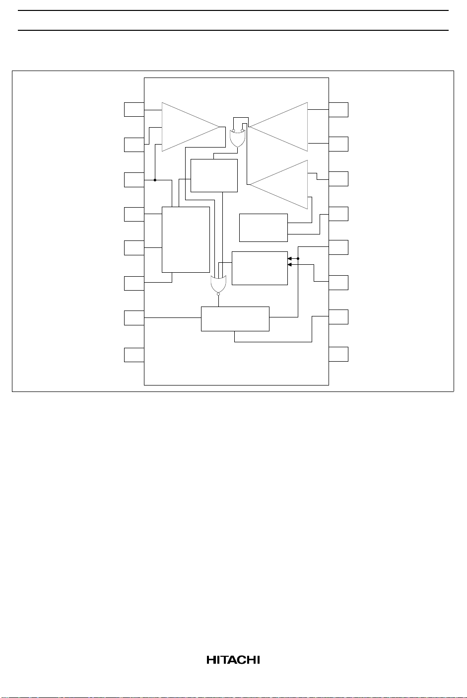
Block Diagram
E/I
ST
C
R
T1
R
T2
OSC Out
GND
N.C
+
1
2
3
T
4
5
6
7
89
PWM
+
comparator
–
R
Triangular
waveform
oscillator
S
S/R
Flip-flop
Output driver
current
detector
Comparator
Reference
voltage
Undervoltage
lockout
protection
Over-
1.3 V
5 V
+
16
–
15
–
14
+
13
12
11
10
N.INV
INV
CS
Vref
V
IN
RM
OUT
N.C
+
–
4

HA16666P/FP
Absolute Maximum Ratings (Ta = 25°C)
Rating
Item Symbol HA16666P HA16666FP Unit
Power supply voltage V
Output current DC I
(Push-pull)
Peak I
Error input V
OSC input voltage V
CS input voltage V
RM input voltage V
RT2 input current I
RT1 input current I
Power dissipation P
IN
O(DC)
O(peak)
EI
OSC
CS
RM
R2
R1
T
Operation temperature Topr –20 to +85 –20 to +85 °C
Storage temperature Tstg –55 to +125 –55 to +125 °C
Notes: 1. Value at 300 ns of switiching time
2. Value at Ta ≤ 45°C. If Ta > 45°C, derated by 8.3 mW/°C
3. Value under the condition of 40 mm × 40 mm × 0.8 t ceramics board epoxy board
+40 +40 V
100 100 mA
500*1 500*
1
mA
Vref Vref V
VIN – 3V
BE
VIN – 3V
BE
V
Vref Vref V
V
IN
V
IN
V
11mA
11mA
680*
2
680*
3
mW
Electrical Characteristics (VIN = 15 V, Ta = 25°C, fosc = 300 kHz)
Item Symbol Min Typ Max Unit Test Condition
Voltage Output voltage Vref 4.75 5.00 5.25 V no load
reference
Triangular Maximum frequency f
waveform
oscillator
Line regulation Line — 50 100 mV V
= 11 to 40 V
IN
Load regulation Load — 9 20 mV IO = 0 to 10 mA
Temperature stability V
Short circuit current I
Minimum frequency f
Frequency accuracy f
Voltage stability f
Temperature coefficient
of frequency
RTC
OS
max
min
der
T
f
i
— +60 — ppm/°C no load
10 35 — mA Vref = 0 V
600 — — kHz CT = 150 pF
— — 1 kHz CT = 0.15 µF
–10 0 +10 %
— 1 — % 11 V≤ VIN ≤ 40 V
— 2 — % –20°C ≤ Ta
≤ +85°C
5
 Loading...