HIT HA16138PS Datasheet

HA16138PS
AC/DC Switching Converter Controller IC
With High-Voltage Power MOS FET
ADE-204-032 (Z)
Preliminary
1st Edition
MAY 2000
Description
The HA16138PS is an IC with a high-voltage power MOS FET and current-mode type PWM controller
mounted in a DILP-8 (DP-8) standard package, suitable for low-power power supplies in the
10 W class and below.
The HA16138PS includes an energy-saving mode for holding down power consumption when on standby
(no load). When the energy-saving mode is entered, the operating frequency is reduced to 1/4 the normal
frequency, reducing power consumption. A starter circuit is also provided on-chip, eliminating the need for
the external start-up resistance needed with previous controller ICs. The starter circuit in this IC is turned
off automatically after the IC starts up, enabling the start-up resistance power consumption to be decreased.
The HA16138PS includes a soft start circuit, OVP circuit, and remote on/off circuit, making it possible to
configure a simple protection circuit with fewer external parts than previously. Also provided are a current
sense resistance and a leading edge blanking circuit that masks spike noise on current sense input, making
noise reduction in a power supply set comparatively easy.
The HA16138PS is equipped with an error amp circuit inverting input (FB) pin and output (COMP) pin,
enabling special-purpose design for both flyback system secondary-side output voltage detection and
primary-side back-up transformer output voltage detection types.
Features
• Built-in high-voltage power MOS FET
• Energy-saving mode (power saving through reduction of operating frequency to 1/4 normal frequency
when on standby)
• Built-in starter circuit, reducing power loss of start-up resistance when on standby (external start-up
resistance not necessary)
• Built-in soft start circuit, eliminating need for external connection
• Remote on/off function, enabling power saving by halting PWM output without turning off power
supply
• Built-in current sense resistance and leading edge blanking circuit, for sense-resistance-less and noise-
cancellation-filter-less implementation
• Built-in over voltage protection circuit
• Built-in over temperature protection circuit

HA16138PS
Pin Arrangement
1DRAIN
2DRAIN
3VDD
4FB
DILP-8
(DP-8)
(Top view)
SOURCE
8
SGND
7
CT
6
COMP
5
Pin Functions
Pin No. Pin Name Pin Function
1 DRAIN On-chip power MOS FET drain pin / starter circuit input pin
2 DRAIN On-chip power MOS FET drain pin / starter circuit input pin
3 VDD Power supply voltage input pin
4 FB Error amplifier inverting input pin / OVP latch circuit input pin
5 COMP Error amplifier output pin
6 CT Timing capacitance connection pin / on/off circuit input pin
7 SGND Primary-side common connection pin
8 SOURCE On-chip power MOS FET source pin
2

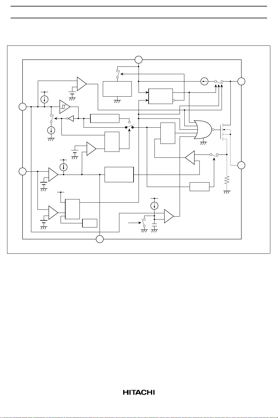
Block Diagram
HA16138PS
VDD
CT
FB
Oscillator
VDD
Vref
−
+
E-AMP
VDD
RSQ
+
−
OVP Latch
+
−
ON/OFF
Comp.
1/4 Divider
+
−
Frequency Down
Comp.
TSD
COMP
Vref
Generator
CK
DQ
1/3
Attenuator
UVL
UVL
FF
Vref
+
−
Soft Start
UVL
CS
Comp.
Leading Edge
Blanking
+
−
Delay
Starter
Driver
DRAIN
SOURCE
Rcs
3

HA16138PS
Absolute Maximum Ratings (Ta = 25°C)
Item Symbol Rating Unit
Power MOS FET block Drain-source voltage V
Maximum drain current I
Controller block Power supply voltage V
CT pin voltage V
FB pin voltage V
COMP pin voltage V
DS
DS
DD
CT
FB
COMP
Overall Operating temperature Topr −20 to +85 °C
Junction temperature Tjmax +150 °C
Storage temperature Tstg −55 to +150 °C
−0.3 to 700 V
0.5 A
0 to 15 V
0 to V
DD
0 to V
DD
0 to 5 V
V
V
4

HA16138PS
Electrical Characteristics (Tj = 25°C, VDD = 12 V, fosc1 = 100 kHz)
Item Symbol Min Typ Max Unit Test Conditions
Power Drain-source voltage BV
MOS FET Drain-source on resistance R
Starter Start-up start drain voltage V
circuit Start-up charge current I
UVL circuit Operation start power supply
V
DS(on)
DRN
CHG
TH
voltage
Operation stop power supply
V
TL
voltage
Operating power supply current I
DD
Oscillation Normal mode operating frequency fosc1 88 100 112 kHz CT = 220 pF
circuit F-down mode operating frequency fosc2 22 25 28 kHz CT = 220 pF, V
Maximum on duty Dumax 70 %
Error Open-loop voltage gain A
V
amplifier Unity gain bandwidth BW 550 kHz Rcomp = 220 kΩ
Output high voltage 1 V
Output high voltage 2 V
Output low voltage V
Non-inverting input voltage V
Power Output rise time t
MOS FET Output fall time t
gate drive Output high voltage V
circuit Output low voltage V
Current Current sense voltage gain A
COMPH1
COMPH2
COMPL
(+)EA
r
f
OH
OL
VCS
sense Current sense response time tpdcs 200 ns Vcomp = 5.0 V
circuit Leading edge blanking time t
BL
OVP latch OVP latch set voltage Vovp 4.2 5.0 5.8 V Vovp: FB pin voltage
circuit OVP latch reset voltage Vovpr 4.0 V Vovpr: VDD pin voltage
OVP latch current dissipation Iovp 1.1 1.7 mA VFB = 6.0 V
Remote
Off mode start voltage Voff 3.6 3.8 4.0 V Voff: CT pin voltage
on/off circuit
Soft start
Soft start time tst (1.0) 2.0 (3.0) ms Time from start-up to
circuit
f-down
F-down mode start voltage Vfdcp 0.7 0.85 1.0 V
comparator
Over
temperature
Over temperature protection start
temperature
TSD 150 °C TSD: Power MOS FET
protection
circuit
700 V
DSS
12 20 Ω ID = 0.4 A
55 75 95 V
125 250 500 µA
10 11 12 V
789V
2.5 4.0 mA
50 65 dB Rcomp = 220 kΩ
4.5 5.0 V Iosource = 0 µA
4.3 4.8 V Iosource = 100 µA
0.50 0.75 V Iosink = 0 µA
3.4 3.8 4.2 V
100 ns CL = 1000 pF
80 ns CL = 1000 pF
10 V Iosource = 25 mA
0.5 V Iosink = 25 mA
3.0 V/V
300 ns
COMP
max. duty
junction temperature
= 0 V
5

HA16138PS
Functional Description
Note: Unless specified otherwise, characteristic values in the text and figures are typical values or design
values.
Starter Circuit
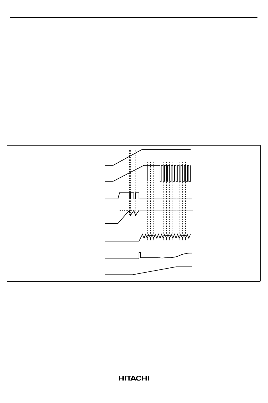
When power is turned on, the starter circuit operates during standby mode, and a constant current is
supplied from the drain pins to the VDD pin. This constant current supplies the external capacitance
charge current for charging up the VDD pin and the standby current consumed by the IC itself while on
standby.
Therefore, the start-up bleeder resistance required by previous products with no on-chip starter circuit is no
longer necessary. The starter circuit detects both the drain voltage and the VDD pin voltage, and controls
VDD so that the IC does not start up if the drain voltage is less than 75 V.
Vb+
0
DRAIN
75V
0
Istart
VDD
CT
COMP
DC
OUTPUT
0
11V
8V
0
0
0
0
Figure 1 Start-Up Timing
UVL Circuit
The UVL circuit is a function that monitors the VDD voltage, and stops IC operation if VDD is low. The
VDD detection voltage has a hysteresis characteristic; the operating start VDD voltage is 11 V, and the
operation stop voltage, 8 V.
In standby mode at the operation stop voltage or below, the UVL circuit keeps the power MOS FET turned
off, and performs control of soft start circuit resetting, internal reference voltage circuit stoppage, and so
forth.
6
 Loading...