

HIT HA16129FPJ Datasheet

HA16129FPJ
Single Watchdog Timer
Description
The HA16129FPJ is a watchdog timer IC that monitors a microprocessor for runaway. In addition to the
watchdog timer function, the HA16129FPJ also provides a function for supplying a high-precision
stabilized power supply to the microprocessor, a power on reset function, a power supply voltage
monitoring function, and a fail-safe function that masks the microprocessor outputs if a runaway is
detected.
Functions
• Watchdog timer (WDT) function
Monitors the P-RUN signal output by the microprocessor, and issues an auto-reset (RES) signal if a
microprocessor runaway is detected.
• Stabilized power supply
Provides power to the microprocessor.
• Power on and clock off functions
The power on function outputs a low level signal to the microprocessor for a fixed period when power
is first applied.
The clock off function outputs a RES signal to the microprocessor a fixed period after a runaway
occurs.
• Power supply monitoring function
When the reference voltage (Vout) falls and becomes lower than the NMI detection voltage (4.63V,
Typ) or the STBY detection voltage (3.0V Typ), this function outputs either an NMI signal or an STBY
signal, respectively. Note that NMI detection can be set to monitor either VCC or Vout.
• OUTE function*1 (fail-safe function)
Outputs a signal used to mask microprocessor outputs when a microprocessor runaway has been
detected.
• RES delay function
Sets the delay between the time the NMI signal is output and the time the RES signal is output.
• Protection functions
The HA16129FPJ incorporates both Vout overvoltage prevention and current limiter functions.
Note: 1. OUTE function: OUTE is an abbreviation for output enable.

HA16129FPJ
Features
• High-precision output voltage: 5.0V ± 1.5%
• The WDT supports both frequency and duty detection schemes.
• High-precision power supply monitoring function: 4.625V ± 0.125V
• Built-in OUTE function
• All functions can be adjusted with external resistors and/or capacitors.
Pin Arrangement
P-RUN
Rf
Cf
R
C
R
C
RES
GND
Voadj
OUTE
20
STBY1
STBYadj
2
3
4
R
5
R
6
T
7
8
9
10
(Top view)
19
18
17
16
15
14
13
12
11
RES
NMI
NMIadj
NMIsns
V
OUT
CONT
CS
V
CC
2
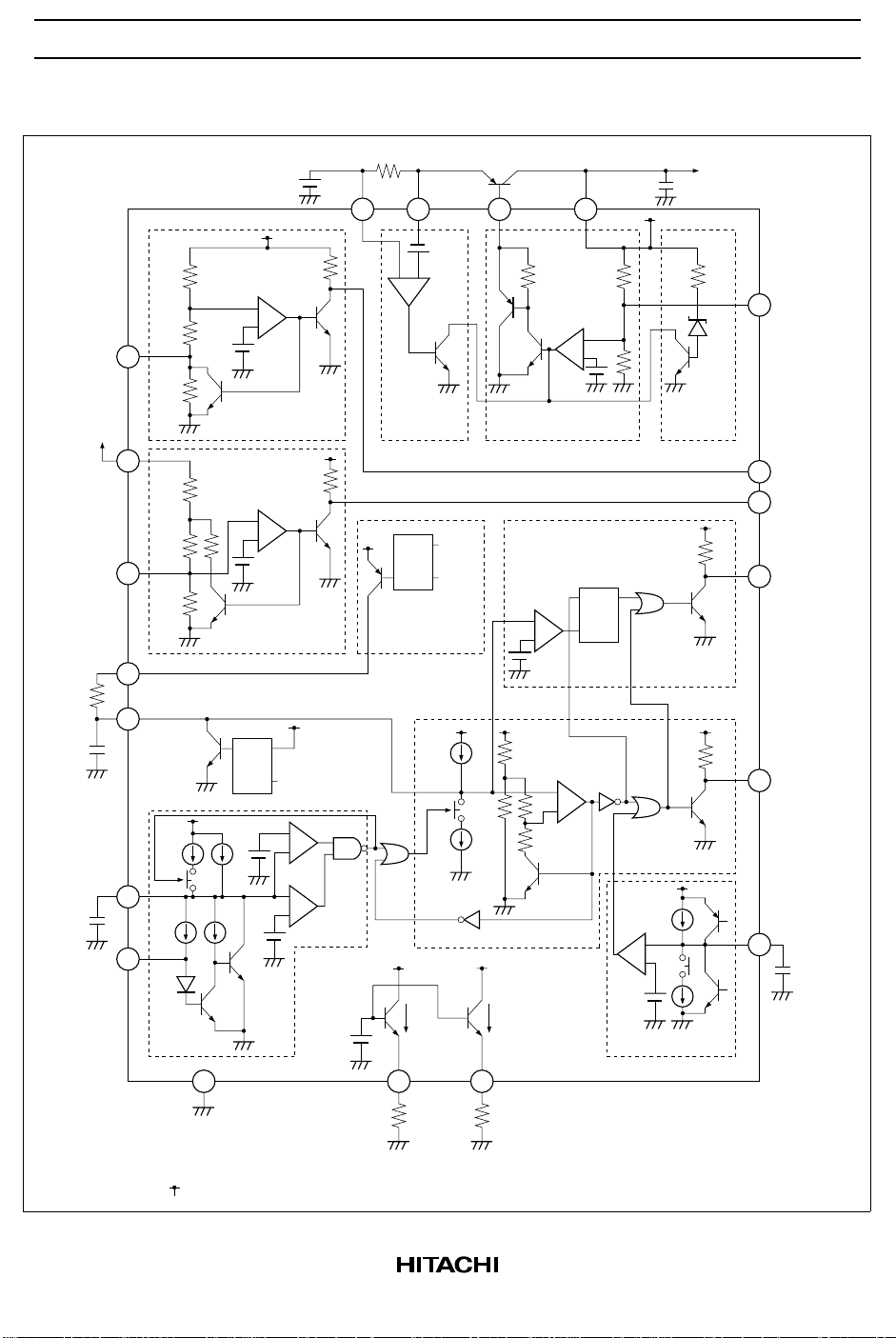
Block Diagram
HA16129FPJ
To microprocessor
(or other device)
V
CC
11
CS CONT
12
13
14
V
OUT
power supply
connections
STBYadj
To Vout
NMIsns
NMIadj
R
C
P-RUN
3.3k
–
+
19
31.2k
36.8k
71k
1.5V
STBY detection
block
15
2k
80k
70k
16
3.3k
–
+
1.18V
25k
NMI detection
T
block
6
150mV
–+
Overcurrent
detection
block
STBY
Q RSRES
tON detection
block
1.24V
–
+
Regulator block
–
+
OUTE
block
Voadj
9
Overvoltage
detection
block
STBY
20
17
NMI
3.3k
10
QRS
OUTE
5
R
If*16
Cf
3
1
If/6
QRS
NMI
–
–
+
–
+
WDT block
I
R
IR*4/3
33k
19k
8.4k
20k
RES block
3.3k
+
–
+
18
7
RES
C
RES
–
8
GND
2V
I
R
4
R
R
If
Delay circuit block
2
Rf
Note: The current, voltage, and resistor values listed in the diagram are reference values.
: Connect to Vout
3

HA16129FPJ
Pin Function
Related
Function
Pin
No. Symbol Function
WDT. 1 P-RUN Watchdog timer pulse input. The auto-reset function is controlled by the
duty cycle or frequency of this input pulse signal.
2 Rf The resistor connected to this pin determines the current that flows in the
Cf pin capacitor. Use the resistor value from 100 kΩ to 500 kΩ
3 Cf The current determined by the Rf pin charges the Cf capacitor and the
potential on this pin determines the watchdog timer frequency band.
tRH, tRL, t
4RRThe resistor connected to this pin determines the current that flows in the
OFF
C
pin capacitor. Use the resistor value from 100 kΩ to 500 kΩ
R
5CRThe current determined by the RR pin charges the capacitor CR and the
potential on this pin controls the RES function (toff, t
t
ON
6RTThe resistor RT, which determines only the time tON for the RES function is
, and tRL).
RH
connected to this pin. This resistor determines the current that charges the
tr, t
RES
7C
RES
capacitor C
The current determined by the Rf pin charges the capacitor C
RES delay times (Tr and T
for the time tON. Use the resistor value from 100 kΩ to 500 kΩ
R
, and the
) are determined by the potential of this
RES
RES
capacitor.
— 8 GND Ground
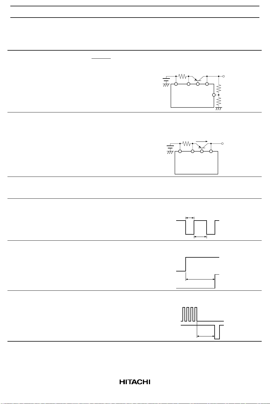
Vout 9 Voadj Insert the resistor Roadj if fine adjustment of the regulator output voltage
Vout is required. Leave this pin open if Vout does not need to be changed.
Output 10 OUTE Output for the OUTE function
Power
11 V
CC
Power supply
supply
Current
limiter
12 CS Current limiter current detection. Connect the overcurrent detection
resistor between the CS pin and the V
short this pin to V
. Also, connect this pin to the emitter of the external
CC
transistor. (This function can not operate when V
pin. If this function is not used,
CC
< 2 V)
OUT
Vout 13 CONT Connect this pin to the base of the external transistor.
14 V
OUT
Provides the regulator output voltage and the IC internal power supply.
Connect this pin to the collector of the external transistor.
NMI 15 NMIsns This pin senses the NMI detection voltage. If VCC is to be detected,
connect this pin to the V
required), and if Vout is to be detected, connect this pin to the V
pin (however, note that an external resistor is
CC
OUT
pin.
16 NMIadj Insert a resistor if fine adjustment of the NMI detection voltage is required.
Leave this pin open if fine adjustment is not required.
Output 17 NMI NMI output
Output 18 RES RES output
STBY 19 STBYadj Insert a resistor if fine adjustment of the STBY detection voltage is
required. Leave this pin open if fine adjustment is not required.
Output 20 STBY STBY output
4

HA16129FPJ
Functional Description
This section describes the functions provided by the HA16129FPJ. See the section on formulas for details
on adjustment methods.
Regulator Block
Vout Voltage
This IC provides a stabilized 5V power supply by controlling the base current of an external transistor. The
largest current (the maximum CONT pin current) that can be drawn by the base of this external transistor is
20mA. Also note that the Vout output is also used for the power supply for this IC’s internal circuits.
Current Limiter Block
When a current detection resistor (RCS) is connected between the VCC pin and the CS pin, and the voltage
between these pins exceeds the VCS voltage (150mV Typ), the CONT pin function turns off and the output
voltage supply is stopped. This function can not work when V
Output Voltage (Vout) Adjustment
The output voltage can be adjusted by connecting an external resistor at the output voltage adjustment pin
(Voadj). However, if for some reason the voltage on this Vout line increases and exceeds the voltage
adjustment range (7V Max), the CONT pin function turns off and the output voltage supply is stopped.
OUT
< 2V.
Refer to the timing charts in conjunction with the following items.
LVI (Low Voltage Inhibit)
NMI Detection Voltage
This function monitors for drops in the power-supply voltage. This function can be set up to monitor either
VCC or Vout. When Vout is monitored, a low level is output from the NMI pin if that voltage falls under the
detection voltage (4.63V Typ). Then, when the power-supply voltage that fell rises again, the NMI pin will
output a high level. Note that this function has a fixed hysteresis of 50mV (Typ). The monitored power
supply is selected by connecting the NMIsns pin either to the VCC pin or to the V
pin. When detecting
OUT
VCC, an external adjustment resistor is required.)
The detection voltage can also be adjusted with the NMIadj pin.
STBY Detection Voltage
This function monitors for drops in the Vout voltage. It monitors the Vout voltage, and outputs a low level
from the STBY pin if that voltage drops below the detection voltage (3.0V Typ). Then, when the powersupply voltage that fell rises again, the STBY pin will output a high level. Note that this function has a
fixed hysteresis of 1.35V (Typ).
The detection voltage can also be adjusted with the STBYadj pin.
5

HA16129FPJ
Function Start Voltage
This is the minimum required Vout voltage for the RES, NMI, STBY, and OUTE output pin functions to
start operating. It is stipulated as the voltage that Vout must reach after power is first applied for these pins
to output a low level.
Hysteresis
This is the difference between the LVI function detection voltage when the power-supply voltage drops,
and the clear (reset) voltage when the power-supply voltage rises.
(V
= V
' – V
; V
= V
HYSN
NMI
NMI
HYSS
STBY
' – V
OUTE Function
When a microprocessor is in the runaway state, its outputs are undefined, and thus it is possible that the
outputs may be driven by incorrect signals. This function is used to mask such incorrect microprocessor
outputs. When the WDT function recognizes normal operation (when the RES output is high), the OUTE
output will be held high. When the WDT function recognizes an abnormal state and an auto-reset pulse is
output from the RES pin, the OUTE output will be held low. Thus microprocessor outputs during
microprocessor runaway can be masked by taking the AND of those outputs and this signal using external
AND gates.
STBY
)
The OUTE output will go high when the CR pin voltage exceeds VthHcr2, and will go low when that
voltage falls below VthLcr.
There are limitation that apply when the OUTE function is used. Refer to the calculation formulas item for
details.
RES Function
t
RH
This period is the length of the high-level output period of the RES pulse when the P-RUN signal from the
microprocessor stops. This is the time required for the CR potential to reach VthLcr from VthHcr1.
t
RL
This period is the length of the low-level output period of the RES pulse when the P-RUN signal from the
microprocessor stops. This is the time required for the CR potential to reach VthHcr1 from VthLcr.
t
OFF
This is the time from the point the P-RUN signal from the microprocessor stops to the point a low level is
output from the RES pin. During normal microprocessor operation, the potential on the CR pin will be
about Vout – 0.2V (although this value may change with the P-RUN signal input conditions, so it should be
verified in the actual application circuit) and t
is the time for the CR pin potential to reach VthLcr from
OFF
that potential.
6

HA16129FPJ
t
ON
tON is the time from the point the NMI output goes high when power is first applied to the point the RES
output goes low. tON is the time for the potential of the CR pin to reach VthHcr1 from 0V.
tr
The time tr is the fixed delay time between the point the NMI output goes from low to high after the powersupply voltage comes up to the point RES goes from low to high. The time tr is the time for the CRES pin
potential to fall from the high voltage (about 1.9V) to Vthcres.
t
RES
The time t
power-supply voltage falls to the point RES goes from high to low. The time t
potential to rise from 0V to Vthcres.
WDT Function
This function determines whether the microprocessor is operating normally or has entered a runaway state
by monitoring the duty or frequency of the P-RUN signal. When this function recognizes a runaway state,
it outputs a reset pulse from the RES pin and sets the OUTE pin to low from high. It holds the RES and
OUTE pins fixed at high as long as it recognizes normal microprocessor operation.
is the fixed delay time between the point the NMI output goes from high to low when the
RES
is the time for the C
RES
RES
pin
In this function, the potential of the Cf capacitor is controlled by the P-RUN signal. This Cf pin potential
charges the capacitor CR that controls the reset pulse to be between VthLcf and VthHcf. The judgment as
to whether or not the microprocessor is operating normally, is determined by the balance between the
charge and discharge voltage on the capacitor CR at this time.
7
HA16129FPJ
Calculation Formulas
Item Formula Notes
Reference
voltage
Vout = 1.225 1 +
(
R1, R2; kΩ
37 // R1
12 // R2
While the Vout voltage will be 5 V ±1.5% when the
(
Voadj pin is open, the circuit shown here should be
used to change the Vout voltage externally.
R1
R2
Current
limiter
voltage
V
(150 mV Typ) < IL · R
CS
CS
VCCCS Vout
Voadj
When this function operates, the base current to the
external transistor connected to the CS pin stops and
the Vout output is lowered.
R
CSIL
VCCCS Vout
OVP — This function prevents the microprocessor from being
damaged if the Vout voltage is inadvertently increased
to too high a level. The OVP detection voltage is fixed.
tRH, t
t
ON
RL
tRH
= 3.3 × C
t
= 1.1 × CR · R
RL
R
· R
tON = 1.1 × CR · R
R
R
T
These determine the reset pulse frequency and duty.
t
RL
RES
t
RH
Sets the time from the rise of the NMI signal to the point
the RES output is cleared.
NMI
t
RES
t
t
OFF
= 6.5 × CR · R
OFF
R
Sets the time from the point the P-RUN pulse stops to
ON
the point a reset pulse is output.
P-RUN
RES
toff
8
 Loading...