HIT HA16117FPCJ, HA16117FPC, HA16117FPBJ, HA16117FPB, HA16117FPAJ Datasheet
...
HA16117F Series
CMOS Watchdog Timer
Description
The HA16117F Series of ICs make a micro-processor (MPU) system fail-safe by monitoring its power
supply to detect voltage drops, and monitoring a P-RUN (program running) pulse to detect system crashes.
Also referred to as watchdog timers, these devices are essential in systems that aim for high levels of crash
protection. Fabricated by a CMOS process, they consume little power and are ideally suited for batteryoperated systems.
These ICs are available in versions for industrial and communications equipment and automotive
applications, as well as for consumer products.
Functions
• Power-on reset
Sends a RES signal to the MPU for a fixed time at power-on
• Watchdog timer (WDT)
Monitors a P-RUN signal from the MPU and sends the MPU a RES signal if P-RUN departs from a
set frequency range
• Auto-reset
Outputs RES signals to the MPU at clocked intervals while P-RUN remains abnormal
• Supply voltage supervision
Outputs a low RES signal if the supply voltage (same as the MPU's VCC) falls below a low threshold
level (VTL). The threshold differs for different ICs in the series, allowing designers to choose an IC
matching system requirements (see ordering information)
Features
• Low power consumption : Operating (ACC pin low) = 0.5 mW (Typ)
: Standby (ACC pin high) = 0.2 mW (Typ)
• Watchdog timer on/off control by ACC input signal
• Independent auto-reset high and low times (tRH and tRL)
• Watchdog monitoring by frequency filtering (independent of duty cycle)
• High-precision low voltage detection (±2%)
• Space- and weight-saving 8-pin SOP package

HA16117F Series
Ordering Information
The HA16117F Series includes three ICs with different low threshold levels (VTL).
Type No. Low Threshold Voltage (VTL)
HA16117FPA/FPAJ 4.4 V Typ
HA16117FPB/FPBJ 4.2 V Typ
HA16117FPC/FPCJ 4.0 V Typ
Pin Arrangement
V
CC
P-RUN
C
C
F
R
8
1
7
2
6
3
5
4
(Top view)
Tadj
ACC
GND
RES
Pin Description
Pin No. Symbol Function
1V
CC
2 P-RUN Watchdog timer (WDT) input
3C
4C
F
R
5 RES Reset signal output from WDT and voltage supervision circuits
6 GND Ground
7 ACC WDT on/off control input (on when ACC is low)
8 Tadj * For adjusting tRH and t
Note: The low-voltage threshold cannot be modified by changing the external resistors connected to the
Tadj pin.
Power supply voltage input
Connected capacitor CF determines WDT filter characteristic
(normal frequency range)
Connected capacitor CR determines tON for power-on reset and t
and t
for auto-reset
RL
(divide VCC to get the adjustment voltage)
OFF
OFF
, tRH,
2
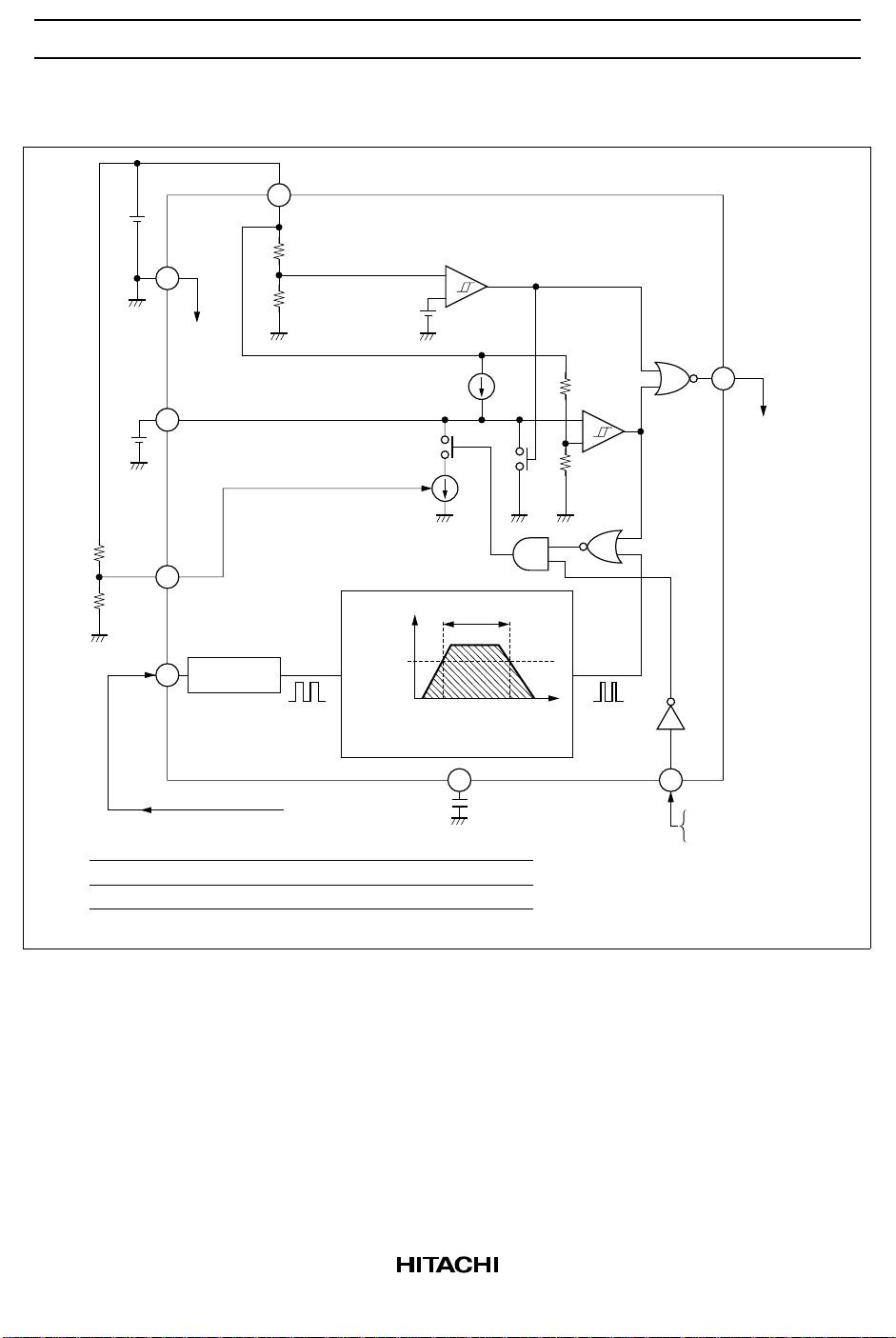
Block Diagram
5 V
6
0.1 µ
4
1
V
CC
2.52 (117FA)
2.36 (117FB)
GND
GND
Power-on and auto-reset circuit
C
R
2.20 (117FC)
1
I2 adjustment
(*I
< I2)
1
Low voltage detector
−
+
≈1.25 V
COMP.
SW2
I
HA16117F Series
RES
I
1
−
+
COMP.
2
SW1
5
to Microcomputer
R
1
510 k
R
2
750 k
Mode
Operating
Standby High
Note: The power-on reset circuit operates in both operating and standby modes.
Tadj
8
P-RUN
1/2 frequency
2
divider
PULSE from I/O port
ACC Voltage Function
Low Low voltage detection and WDT
(SW1 and SW2 are active high)
Watchdog timer
Watchdog filter (f-duty converter)
W.D out
duty (%)
W.D in
duty 50%
Low voltage detection
n
Normal range
f
/2 fH/2
L
W.D in frequency (Hz)
C
F
3 7
0.01 µ
W.D out
duty n%
ACC
Operating: "Low"
Standby: "High"
The HA16117F consists of a low voltage detector, power-on and auto-reset circuit, and watchdog timer.
Low Voltage Detector
Uses a reference voltage source (≈ 1.25 V) and high-precision comparator to detect drops in the supply
voltage.
Power-On and Auto-Reset Circuit
Generates the RES waveform, using a multivibrator consisting of a current source I1 that charges the
external capacitor CR, a current source I2 that discharges CR, and a comparator.
3

HA16117F Series
Watchdog Timer
Reshapes the P-RUN signal (programming-running pulse) from the MPU to obtain a 50% duty cycle, then
converts frequency to duty cycle in the watchdog filter (WD filter).
The watchdog filter is a bandpass filter. The duty cycle of the filter output is highest in the normal
frequency range of P-RUN.
The watchdog filter output controls I2 in the multivibrator, the higher the duty cycle of the watchdog filter
output, the shorter the time during which I2 discharges CR. If the duty cycle is high enough then CR is held
at a high potential, preventing the multivibrator from firing, and the RES output remains high.
Absolute Maximum Ratings (Ta = 25°C)
Ratings
Item Symbol HA16117FPA/FPB/FPC HA16117FPAJ/FPBJ/FPCJ Unit
Power supply voltage V
P-RUN input voltage V
ACC input voltage V
RES output current I
Permissible dissipation *
1
CC
P
ACC
RES
P
T
Operating temperature range Topr –30 to +85 –40 to +85 °C
Storage temperature Tstg –55 to +125 –55 to +125 °C
Note: 1. This is the value when mounted on a glass epoxy substrate with 30% wiring density, up to an
ambient temperature of 83°C. Above that temperature, derate by 7.14 mW/°C.
–0.3 to +14 –0.3 to +14 V
V
CC
V
CC
V
14 14 V
10 10 mA
300 300 mW
40mm
(mW)
T
400
60 80
83°C
85°C
100
300
200
100
0
−30 −20 0 20 40
Ambient operating temperature range Ta (°C)
Permissible dissipation P
−7.14 mW/°C
(30% wiring density)
Substrate
0.8 mm ceramic or
1.5 mm epoxy
4

HA16117F Series
Electrical Characteristics
(VCC = 5 V, Ta = 25°C, CF = 0.01 µF, CR = 0.1 µF, R1 = 510 kΩ, R2 = 750 kΩ)
Item Symbol Min Typ Max Unit Test Conditions
General Operating supply current I
Standby supply current I
Low
voltage
detector
Low voltage
threshold
level
HA16117FPA/FPAJ V
HA16117FPB/FPBJ 4.1 4.2 4.3 V
HA16117FPC/FPCJ 3.9 4.0 4.1 V
Hysteresis width V
ACC Low input voltage V
High input voltage V
P-RUN Low input voltage V
input High input voltage V
WDT Power-on reset time t
Reset-clock off time t
Reset low time t
Reset high time t
Low setup time t
High setup time t
RES RES low voltage V
output RES high voltage V
Reset function starting voltage V
Constant
Constant range of R1 and R
2
range
Operating supply voltage range V
Note: 1. Reset-clock off time t
is provided a shown in the under figure.
OFF
CC1
I
CC2
STBY
TL
HYS
IL1
IH1
IL2
IH2
ON
OFF
RL
RH
SL
SH
OL
OH
RES
K 0.55 0.6 0.8 — K =R2 / (R1 + R2)
CCRNG
— 100 — µAV
— 200 600 µAV
— 43 100 µAV
4.3 4.4 4.5 V
50 100 150 mV
— — 0.8 V
2.0 — — V
— — 0.8 V
2.0 — — V
24 40 56 ms
1
*
78 130 182 ms
12 20 28 ms
36 60 84 ms P-RUN pin = 0 V
1——ms
——1 ms
— — 0.4 V IOL = 1 mA
—VCC— V Open
— 0.8 1.4 V
V
TL
— 6.0 V
= 0 V,
ACC
f
= 100 Hz
P-RUN
= 0 V,
ACC
f
= 20 kHz
P-RUN
= 12 V
ACC
When VCC drops
P-RUN
RES
f = 500 Hz, Duty = 50%
t
OFF
5
HA16117F Series
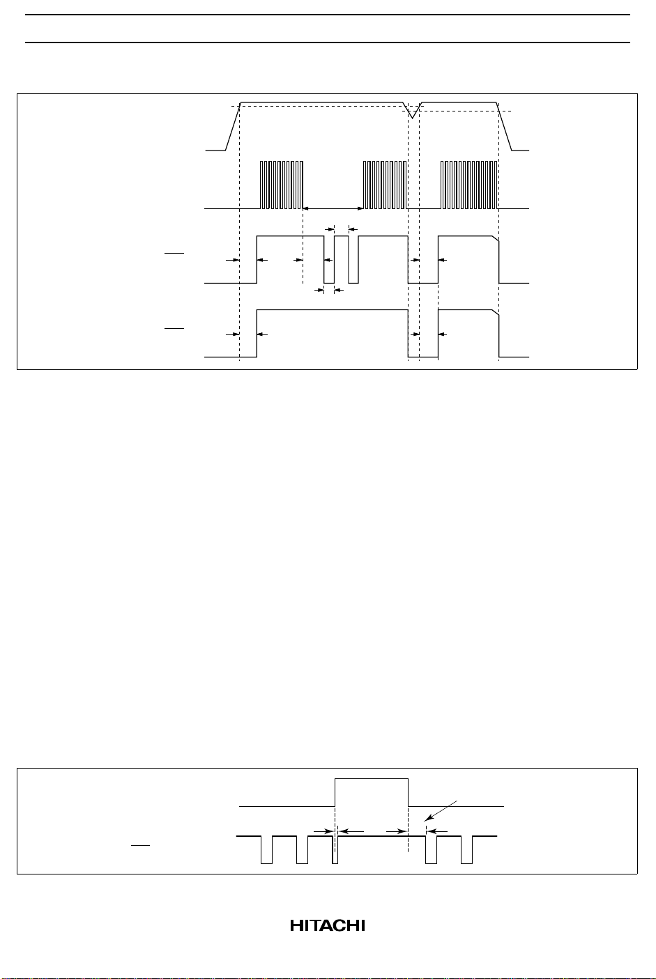
Timing Waveforms and Functional Description
V
CC
V
TL
P-RUN
Watchdog function on
RES
(V
= "Low")
ACC
Watchdog function off
RES
(V
= "High")
ACC
t
ON
t
ON
Crash
t
RH
t
OFF
t
RL
t
ON
t
ON
Figure 1 Timing Waveforms
Watchdog On/Off Function
A feature of the HA16117F is that watchdog supervision can be switched on and off. When the watchdog
function is switched on, both the supply voltage and
P-RUN input are monitored to detect abnormal conditions. When the watchdog function is switched off
(standby mode), only the supply voltage is monitored. Watchdog supervision is switched on and off by the
input at the ACC pin (pin 7): Supervision is on when ACC is low, and off when ACC is high.
Many MPUs have a standby mode in which the CPU stops running but memory contents are retained. In
standby mode, program execution halts and I/O ports go to the high-impedance state, so there is no need for
the watchdog timer to supervise pulse output from an I/O port to detect abnormal conditions. Power can be
saved by placing both the MPU and HA16117F in standby mode at the same time. The HA16117F is
designed to draw a typical standby current I
of only 43 µA Typ when the watchdog function is switched
STBY
off.
ACC Pin (pin 7) and RES Output
When the MPU returns from standby mode to normal operation it generally takes 10 to 200 ms for the
clock oscillator in the MPU to stabilize. The RES signal is not output during this setup time. After the
setup time (tSL) has elapsed, RES is output if the P-RUN signal from the MPU is still abnormal.
ACC pin
RES (due to MPU crash)
t
SH
Adjust according to
MPU’s setup time
t
SL
Figure 2 ACC Pin and RES Output
6
HA16117F Series
Internal Operation and Usage Notes
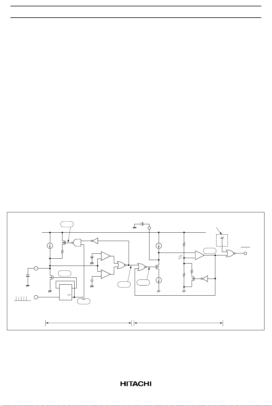
Figure 3 shows an equivalent circuit of the watchdog timer block with a VCC pin level of 5 V and ACC pin
level of 0 V, and the following pages show internal operation timing charts for different P-RUN
frequencies. (Descriptions apply to conditions CF = 0.01 µF, CR = 0.1 µF, R2/(R1 + R2) = 0.6.)
Operation
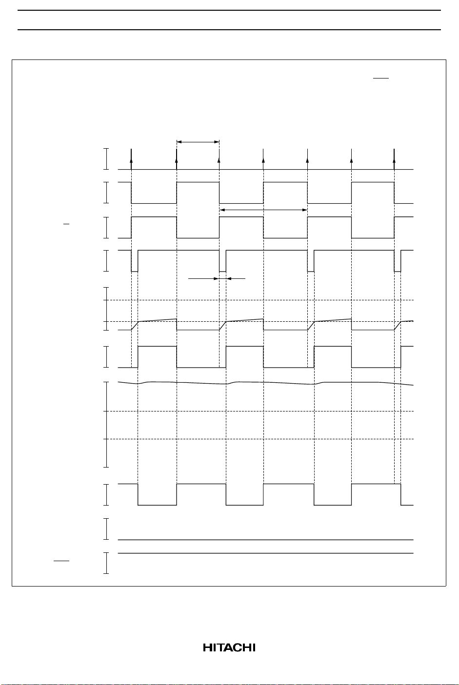
The power-on and auto-reset circuit is a multivibrator with timing controlled by CR charge current I1 and
discharge current I2. As I1 : I2 ≈ 3 : 1 (Typ design value), when the (WD) (watchdog filter circuit output)
on-duty is 25% or above, the CR pin potential does not fall below 1.6 V. Therefore, (C) in the figure below
is fixed low, and RES is not output. The (WD) on-duty varies according to the P-RUN frequency. If the
frequency is lower or higher than the design value, the (WD) on-duty decreases, and at 25% or below, RES
is output. Refer to the timing charts on the following pages for an explanation of the operation of the
watchdog filter.
Usage Notes
• When the P-RUN frequency reaches 20 kHz or above, t
is short (see the timing charts on the
OFF
following pages). This must be borne in mind in the design stage.
• If the P-RUN frequency fluctuates, RES may also be output within the normal detection set frequency
(see the timing charts on the following pages).
• Detection frequencies fH and fL described in the Data Book are Typ values, and a certain amount of
dispersion can be expected. A margin of ±30% or more should be allowed for in the design.
0.1 µ
B
C
R
I
1
8 µ typ
3.2 V
1.6 V
I
2
10.7 µ
typ
Power-on and auto-reset circuitWatchdog filter circuit
Low voltage detection block
C
−
+
RES
I
w
0.8 µ
typ
C
F
0.01 µ
P-RUN
A
3.6 V
Q
QD
φ
Q
1/2
frequency divider
0.9 V
Q
VCC (5 V)
−
+
−
+
WD
Figure 3 Watchdog Timer Evaliation Circuit
7

HA16117F Series
1. When P-RUN signal is not input
P-RUN
C
WD
The watchdog filter circuit output (WD) is fixed low, so the RES signal is output as shown in
the figure below in accordance with power-on and auto-reset circuit C
H
L
H
Q
L
H
Q
L
H
A
L
5 V
3.6 V
F
0.9 V
0 V
H
L
5 V
charge/discharge.
R
3.2 V
C
R
1.6 V
0 V
H
B
L
H
C
L
H
RES
L
20 ms
60 ms
8
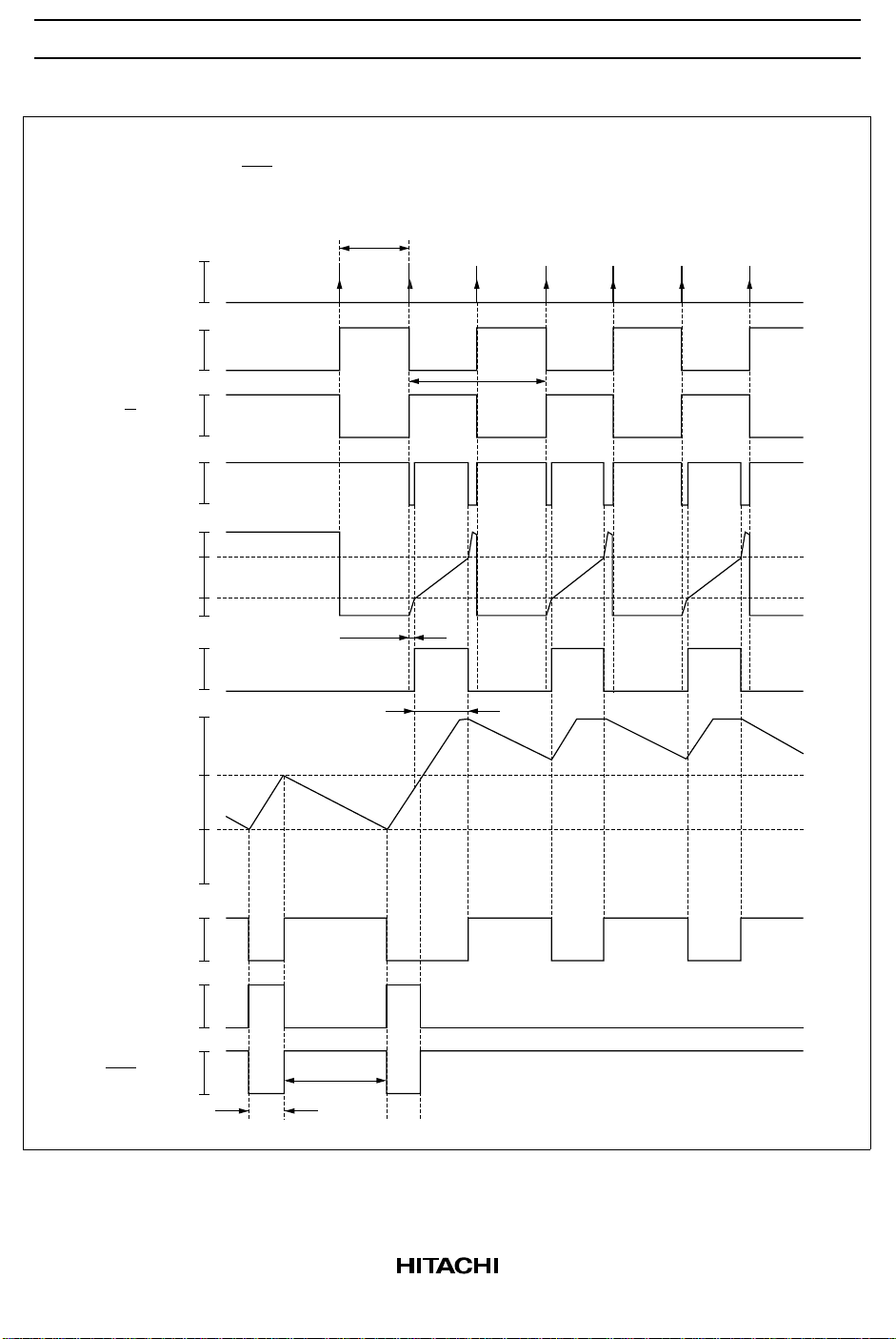
2. With a low-frequency P-RUN signal ( 13 Hz to 26 Hz)
HA16117F Series
P-RUN
C
WD
When f
duty is 25% or above, multivibrator (power-on and auto-reset circuit) oscillation stops. As a
is 13 Hz to 26 Hz, the WD duty (D = 100 × t2/2T) is 25% to 50%. When the WD
P-RUN
result, the RES signal is fixed high.
40 ms (25 Hz)
H
L
H
Q
L
H
2T
Q
L
H
A
L
5 V
3.6 V
F
0.9 V
0 V
5 µs
t
1
H
t
L
2
33 ms
5 V
C
RES
3.2 V
R
1.6 V
0 V
H
B
L
H
C
L
H
60 ms
L
20 ms
9
HA16117F Series
3. With a 10 kHz P-RUN signal
P-RUN
C
WD
When f
25%, the multivibrator (power-on and auto-reset circuit) does not oscillate. The RES signal
remains high.
H
L
H
Q
L
H
Q
L
H
A
L
5 V
3.6 V
F
0.9 V
0 V
H
L
5 V
is 10 kHz, the WD duty (D = 100 × (T − t2)/2T) is 48%. As the duty is above
P-RUN
100 µs (10 kHz)
2T
t
µs
1 5
10
C
RES
3.2 V
R
1.6 V
0 V
H
B
L
H
C
L
H
L
 Loading...