HIT HA16114P, HA16114FPJ, HA16114FP, HA16120FPJ, HA16120FP Datasheet

HA16114P/PJ/FP/FPJ, HA16120FP/FPJ
Switching Regulator for Chopper Type DC/DC Converter
Description
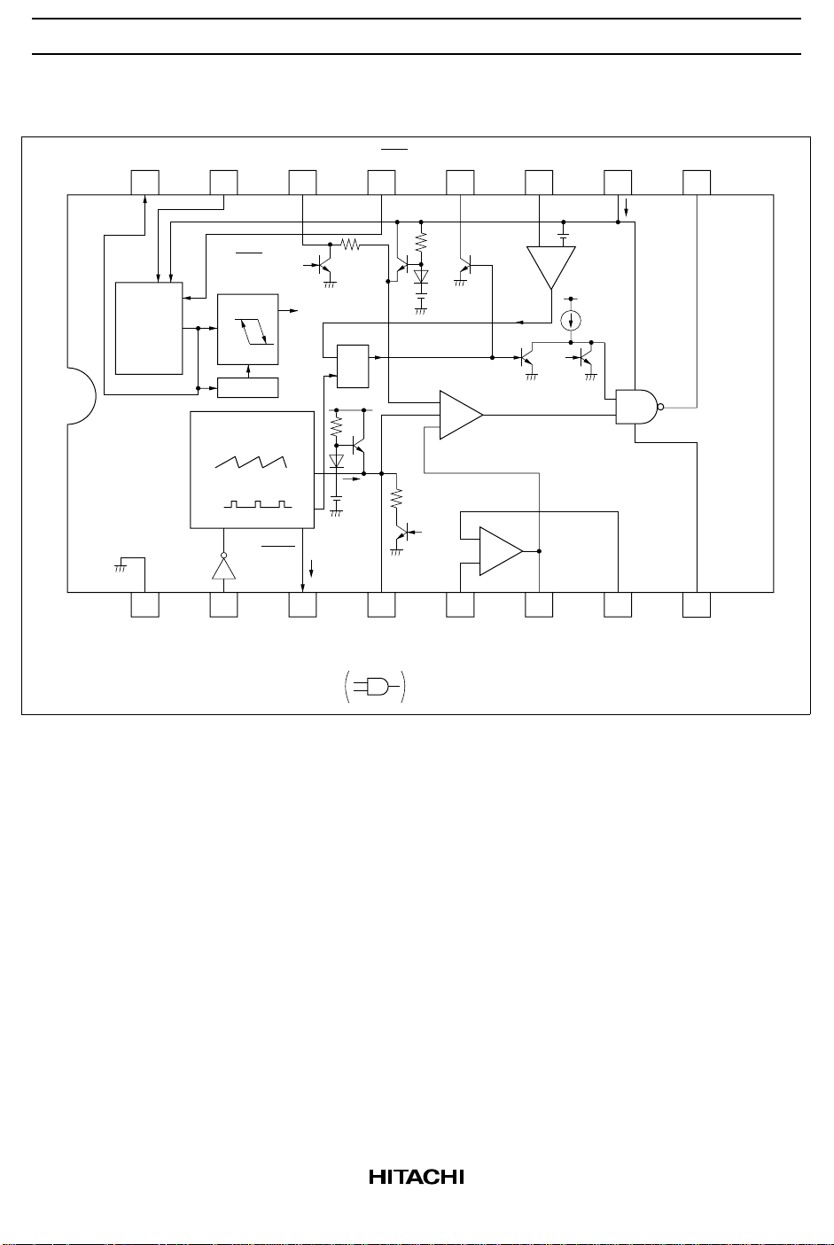
The HA16114P/FP/FPJ and HA16120FP/FPJ are single-channel PWM switching regulator controller ICs
suitable for chopper-type DC/DC converters. Integrated totem-pole output circuits enable these ICs to
drive the gate of a power MOSFET directly. The output logic of the HA16120 is designed to control a
DC/DC step-up (boost) converter using an N-channel power MOS FET. The output logic of the HA16114
is designed to control a DC/DC step-down (buck) converter or inverting converter using a P-channel power
MOS FET.
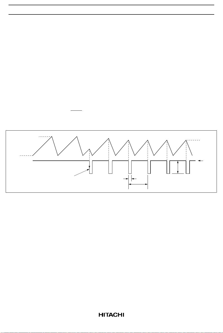
These ICs can operate synchronously with external pulse, a feature that makes them ideal for power
supplies that use a primary-control AC/DC converter to convert commercial AC power to DC, then use one
or more DC/DC converters on the secondary side to obtain multiple DC outputs. Synchronization is with
the falling edge of the ‘sync’ pulse, which can be the secondary output pulse from a flyback transformer.
Synchronization eliminates the beat interference that can arise from different operating frequencies of the
AC/DC and DC/DC converters, and reduces harmonic noise. Synchronization with an AC/DC converter
using a forward transformer is also possible, by inverting the ‘sync’ pulse.
Overcurrent protection features include a pulse-by-pulse current limiter that can reduce the width of
individual PWM pulses, and an intermittent operating mode controlled by an on-off timer. Unlike the
conventional latched shutdown function, the intermittent operating function turns the IC on and off at
controlled intervals when pulse-by-pulse current limiting continues for a programmable time. This results
in sharp vertical settling characteristics. Output recovers automatically when the overcurrent condition
subsides.
Using these ICs, a compact, highly efficient DC/DC converter can be designed easily, with a reduced
number of external components.
Functions
• 2.5 V voltage reference
• Sawtooth oscillator (Triangle wave)
• Overcurrent detection
• External synchronous input
• Totem-pole output
• Undervoltage lockout (UVL)

HA16114P/PJ/FP/FPJ, HA16120FP/FPJ
• Error amplifier
• Vref overvoltage protection (OVP)
Features
• Wide supply voltage range: 3.9 V to 40 V*
• Maximum operating frequency: 600 kHz
• Able to drive a power MOS FET (±1 A maximum peak current) by the built-in totem-pole gate pre-
driver circuit
• Can operate in synchronization with an external pulse signal, or with another controller IC
• Pulse-by-pulse overcurrent limiting (OCL)
• Intermittent operation under continuous overcurrent
• Low quiescent current drain when shut off by grounding the ON/OFF pin
HA16114: I
HA16120: I
• Externally trimmable reference voltage (Vref): ±0.2 V
• Externally adjustable undervoltage lockout points (with respect to VIN)
• Stable oscillator frequency
• Soft start and quick shut function
= 10 µA (max)
OFF
= 150 µA (max)
OFF
Note: The reference voltage 2.5 V is under the condition of VIN ≥ 4.5 V.
Ordering Information
Hitachi Control ICs for Chopper-Type DC/DC Converters
Product Channel Control Functions Overcurrent
Channels Number No. Step-Up Step-Down Inverting Output Circuits Protection
Dual HA17451 Ch 1 ❍❍ ❍Open collector SCP with timer (latch)
Ch 2 ❍❍ ❍
Single HA16114 —— ❍❍Totem pole Pulse-by-pulse
HA16120 — ❍ — — power MOS FET current limiter and
Dual HA16116 Ch 1 — ❍❍driver intermittent operation
Ch 2 — ❍ — by on/off timer
HA16121 Ch 1 — ❍❍
Ch 2 ❍ ——
2

Pin Arrangement
GND*
HA16114P/PJ/FP/FPJ, HA16120FP/FPJ
1
116
Vref
SYNC
IN(−)
IN(+)
P.GND*
215
314
R
T
C
413
T
512
E/O
611
710
1
8
ADJ
DB
ON/OFF
TM
CL(−)
V
IN
OUT9
(Top view)
Note: 1. Pin 1 (GND) and Pin 8 (P.GND) must be connected each other with external wire.
Pin Description
Pin No. Symbol Function
1 GND Signal ground
2 SYNC External sync signal input (synchronized with falling edge)
3R
4C
T
T
5 IN(–) Inverting input to error amplifier
6 E/O Error amplifier output
7 IN(+) Non-inverting input to error amplifier
8 P.GND Power ground
9 OUT Output (pulse output to gate of power MOS FET)
10 V
IN
11 CL(–) Inverting input to current limiter
12 TM Timer setting for intermittent shutdown when overcurrent is detected (sinks
13 ON/OFF IC on/off control (off below approximately 0.7 V)
14 DB Dead-band duty cycle control input
15 ADJ Reference voltage (Vref) adjustment input
16 Vref 2.5 V reference voltage output
Oscillator timing resistor connection (bias current control)
Oscillator timing capacitor connection (sawtooth voltage output)
Power supply input
timer transistor current)
3
HA16114P/PJ/FP/FPJ, HA16120FP/FPJ
Block Diagram
Vref ADJ DB ON/OFF TM CL(−)V
IN
OUT
16 15 14 13 12 11 10 9
0.2 V
+
−
EA
− +
CL
from
UVL
Vref
*1
OUT
NAND (HA16114)
ADJ V
2.5V
bandgap
reference
voltage
generator
IN
ON/OFF
from
UVL
UVL
H
L
V
LVH
OVP
Triangle waveform
generator
1.6 V
1.0 V
Latch reset pulses
1.1 V
R
Bias
UVL
output
T
1k
Latch
SRQ
V
IN
0.3 V
0.3V
PWM COMP
+
−
+
1k
from
UVL
current
12345678
GND
SYNC R C IN(−) E/O IN(+) P.GND
TT
Note: 1. The HA16120 has an AND gate.
4
HA16114P/PJ/FP/FPJ, HA16120FP/FPJ
Timing Waveforms
Generation of PWM pulse output from sawtooth wave (during steady-state operation)
Dead-band
voltage (at DB)
Sawtooth wave
(at C )
T
Error amplifier
output (at E/O)
HA16114 PWM
pulse output
(drives gate of
P-channel
power MOS FET)
V
IN
0 V
Off
Off Off Off
1.6 V typ
1.0 V
typ
On On On OnOn
T =
1
f
OSC
Off
HA16120 PWM
pulse output
(drives gate of
N-channel
power MOS FET)
Note: On duty =
V
IN
0 V
Off Off Off OffOff
On On On OnOn
Time t
t
ON
T
5
HA16114P/PJ/FP/FPJ, HA16120FP/FPJ
Guide to the Functional Description
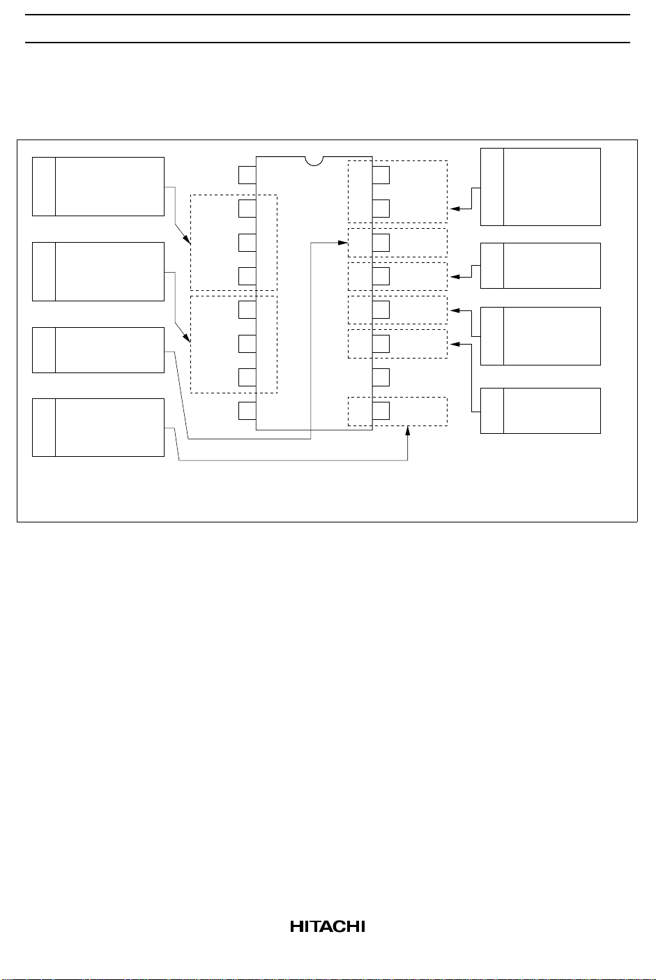
The description covers the topics indicated below.
Oscillator
frequency
1.
(f ) control and
OSC
synchronization
DC/DC output
voltage setting
2.
and error
amplifier usage
Dead-band and
3.
soft-start settings
Output stage and
4.
power MOS FET
driving method
Note: 1.
P.GND is a high-current (±1 A maximum peak) ground pin connected to the totem-pole output circuit.
GND is a low-current ground pin connected to the Vref voltage reference. Both pins must be grounded.
P.GND*
GND*
SYNC
IN(−)
E/O
IN(+)
1
R
T
C
T
1
1. Sawtooth Oscillator (Triangle Wave)
1
2
3
4
5
6
7
8
(Top view)
16
15
14
13
12
11
10
Vref adjustment,
Vref
ADJ
DB
ON/OFF
TM
CL(−)
V
IN
OUT
9
undervoltage
lockout, and
5.
overcurrent
protection
ON/OFF pin
6.
usage
Intermittent
mode timing
7.
during
overcurrent
Setting of
8.
current limit
1.1 Operation and Frequency Control
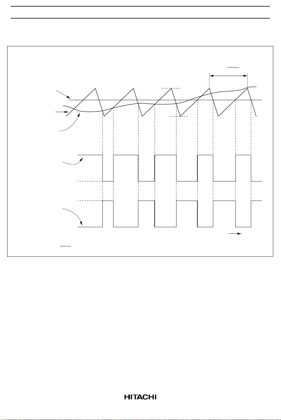
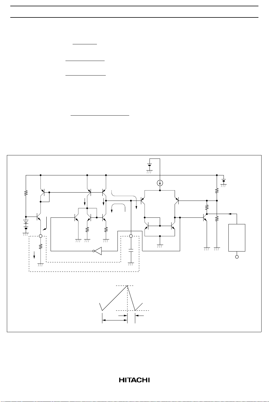
The sawtooth wave is a voltage waveform from which the PWM pulses are created (See figure 1). The
sawtooth oscillator operates as follows. A constant current IO determined by an external timing resistor R
is fed continuously to an external timing capacitor CT. When the CT pin voltage exceeds a comparator
threshold voltage VTH, the comparator output opens a switching transistor, allowing a 3IO discharge current
to flow from CT. When the CT pin voltage drops below a threshold voltage VTL, the comparator output
closes the switching transistor, stopping the 3IO discharge. Repetition of these operations generates a
sawtooth wave.
The value of IO is 1.1 V/RT Ω . The IO current mirror has a limited current capacity, so RT should be at least
5 kΩ (IO ≤ 220 µA).
Internal resistances RA, RB, and RC set the peak and valley voltages VTH and VTL of the sawtooth waveform
at approximately 1.6 V and 1.0 V.
6
T
HA16114P/PJ/FP/FPJ, HA16120FP/FPJ
The oscillator frequency f
f
OSC
Here,
t
=
1
t2 =
can be calculated as follows.
OSC
=
1
t
+ t2 + t
1
C
× (VH − VL)
T
1.1 V/R
C
× (VH − VL)
T
3 × 1.1 V/R
3
T
T
t3 ≈ 0.8 µs (comparator delay time)
Since
VH − VL = 0.6 V
f
≈
OSC
0.73 × C
1
× RT + 0.8 (µs)
T
(Hz)
At high frequencies the comparator delay causes the sawtooth wave to overshoot the 1.6 V threshold and
undershoot the 1.0 V threshold, and changes the dead-band thresholds accordingly. Select constants by
testing under implementation conditions.
3.2 V
1.1 V
Current
mirror
(Internal voltage)
1 : 4
C charging
T
I
O
Discharg
-ing 3I
O
Oscillator
comparator
R
C
Vref
2.5 V
R
A
R
B
Sync
circuit
R
T
C
T
I
O
External circuit
V = 1.6 V typ
H
t
2
t
1
V = 1.0 V typ
L
t1 : t2 = 3 : 1
SYNC
Figure 1.1 Equivalent Circuit of Oscillator
7
HA16114P/PJ/FP/FPJ, HA16120FP/FPJ
1.2 External Synchronization
These ICs have a sync input pin so that they can be synchronized to a primary-control AC/DC converter.
Pulses from the secondary winding of the switching transformer should be dropped through a resistor
voltage divider to the sync input pin. Synchronization takes place at the falling edge, which is optimal for
multiple-output power supplies that synchronize with a flyback AC/DC converter.
The sync input pin (SYNC) is connected internally through a synchronizing circuit to the sawtooth
oscillator to synchronize the sawtooth waveform (see figure 1.2).
• Synchronization is with the falling edge of the external sync signal.
• The frequency of the external sync signal must be in the range f
• The duty cycle of the external sync signal must be in the range 5% < t1/t2 < 50% (t1 = 300 ns Min).
• With external synchronization, VTH' can be calculated as follows.
f
VTH’ = (VTH − VTL) × + V
OSC
f
SYNC
TL
Note: When not using external synchronization, connect the SYNC pin to the Vref pin.
V (1.6 V typ)
TH
Sawtooth wave
(f
)
OSC
V
TL
(1.0 V typ)
SYNC pin
(f
)
SYNC
Synchronized
at falling edge
OSC
t
2
< f
t
1
SYNC
< f
OSC
× 2.
1 V
V
TH
Vref
Figure 1.2 External Synchronization
8
HA16114P/PJ/FP/FPJ, HA16120FP/FPJ
2. DC/DC Output Voltage Setting and Error Amplifier Usage
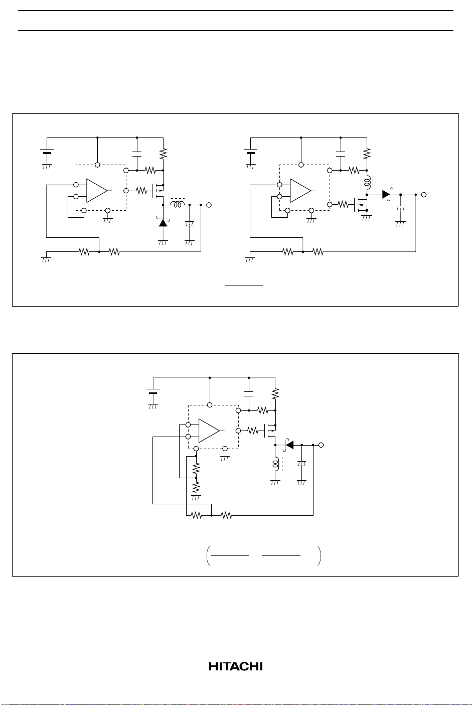
2.1 DC/DC Output Voltage Setting
(1) Positive Output Voltage (VO > Vref)
HA16114 with step-down topology HA16120 with step-down (boost) topology
C
IN(−)
IN(+)
V
IN
−
+
EA
GND
L
OUT
Vref
R
R
2
1
Figure 2.1 Output Voltage Setting (1)
(2) Negative Output Voltage (VO < 0 V)
HA16114 with inverting topology
IN(−)
IN(+)
V
O
+
−
V = VrefO×
V
IN
−
+
Vref
R
3
R
4
EA
C
IN(−)
IN(+)
V
IN
−
+
EA
GND
L
OUT
V
O
+
−
Vref
R
+ R
R
1
2
R
2
C
L
R
2
1
OUT
−
+
R
V = −VrefO×
2
R
1
R + R
12
R
2
R
×− 1
3
R + R
34
Figure 2.2 Output Voltage Setting (2)
9
HA16114P/PJ/FP/FPJ, HA16120FP/FPJ
2.2 Error Amplifier Usage
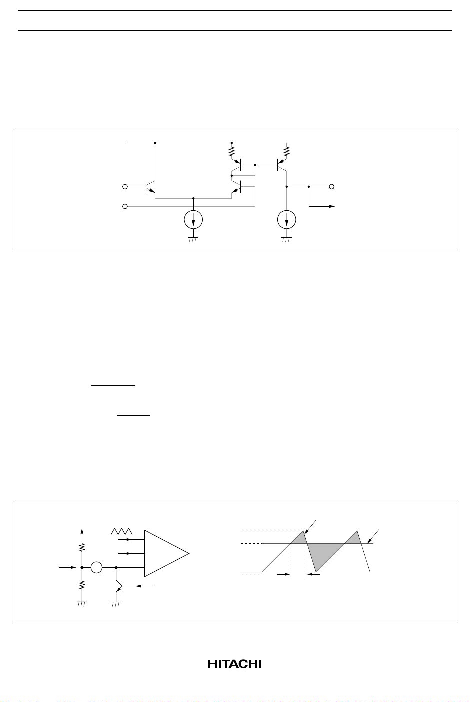
Figure 2.3 shows an equivalent circuit of the error amplifier. The error amplifier in these ICs is a simple
NPN-transistor differential amplifier with a constant-current-driven output circuit.
The amplifier combines a wide bandwidth (fT = 4 MHz) with a low open-loop gain (50 dB Typ), allowing
stable feedback to be applied when the power supply is designed. Phase compensation is also easy.
IC internal V
IN(−)
IN(+)
IN
E/O
To internal PWM
comparator
µµ
40 A80 A
Figure 2.3 Error Amplifier Equivalent Circuit
3. Dead-Band Duty Cycle and Soft-Start Settings
3.1 Dead-Band Duty Cycle Setting
The dead-band duty cycle (the maximum duty cycle of the PWM pulse output) can be programmed by the
voltage VDB at the DB pin. A convenient way to obtain VDB is to divide the IC’s Vref output by two
external resistors. The dead-band duty cycle (DB) and VDB can be calculated as follows.
− V
V
TH
DB = ⋅ ⋅ ⋅ ⋅ This applies when VDB > VTL.
VTH − V
VDB = Vref ×
DB
TL
R
2
R1 + R
× 100 (%)
2
If V
< VTL, there is no PWM output.
DB
Note: VDB is the voltage at the DB pin.
VTH: 1.6 V (Typ)
VTL: 1.0 V (Typ)
Vref is typically 2.5 V. Select R1 and R2 so that 1.0 V ≤ VDB ≤ 1.6 V.
Sawtooth
DB
wave
E/O
PWM
COMP
−
+
+
from
UVL
V
TH
V
DB
V
TL
VTH and VTL vary depending on the oscillator.
Note:
Select constants by testing under implementation
conditions.
To Vref
R
1
V
DB
R
2
Figure 3.1 Dead-Band Duty Cycle Setting
10
Sawtooth wave
Dead band
Voltage at DB pin
HA16114P/PJ/FP/FPJ, HA16120FP/FPJ
3.2 Soft-Start Setting
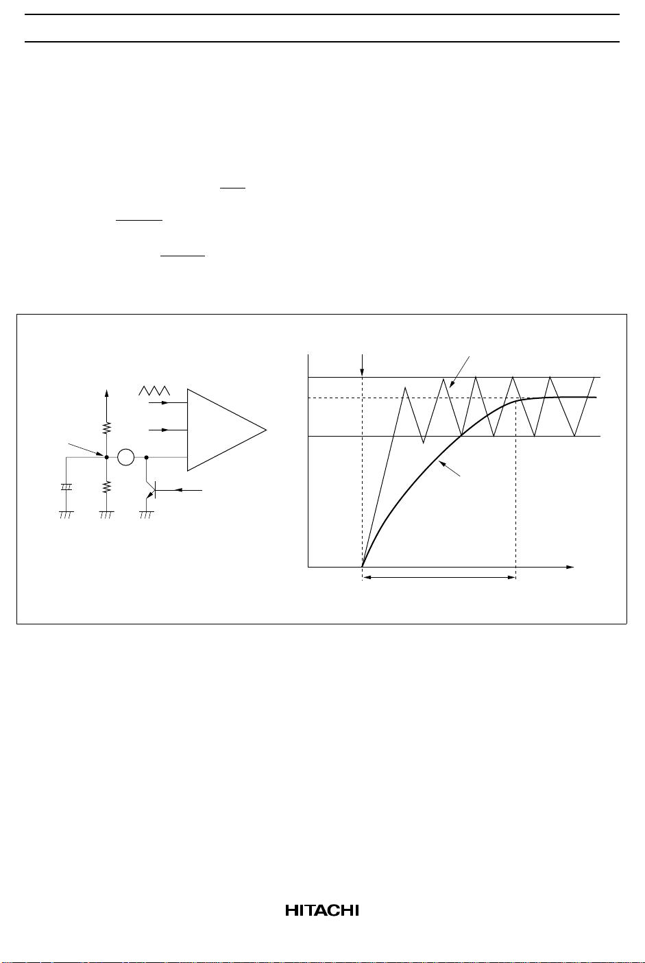
Soft-start avoids overshoot at power-up by widening the PWM output pulses gradually, so that the
converted DC output rises slowly. Soft-start is programmed by connecting a capacitor between the DB pin
and ground. The soft-start time is determined by the time constant of this capacitor and the resistors that
set the voltage at the DB pin.
V
t
= −C1 × R × ln (1 − )
soft
R
× R
1
R1 + R
2
2
R1 + R
R
2
R =
VDB = Vref ×
Note: VX is the voltage at the DB pin after time t (VX < VDB).
To Vref
R
V
X
1
Sawtooth
wave
E/O
DB
X
V
DB
2
Undervoltage
lockout released
1.6 V
V
PWM
COMP
−
+
+
TH
V
DB
V
TL
1.0 V
Sawtooth wave
C
R
1
2
from
UVL
V
X
UVL sink
transistor
t
Soft-start time
t
soft
Figure 3.2 Soft-Start Setting
3.3 Quick Shutdown
The quick shutdown function resets the voltages at all pins when the IC is turned off, to assure that PWM
pulse output stops quickly. Since the UVL pull-down resistor in the IC remains on even when the IC is
turned off, the sawtooth wave output, error amplifier output, and DB pin are all reset to low voltage.
This feature helps in particular to discharge capacitor C1 in figure 3.2, which has a comparatively large
capacitance. In intermittent mode (explained on a separate page), this feature enables the IC to soft-start in
each on-off cycle.
11
HA16114P/PJ/FP/FPJ, HA16120FP/FPJ
4. PWM Output Circuit and Power MOSFET Driving Method
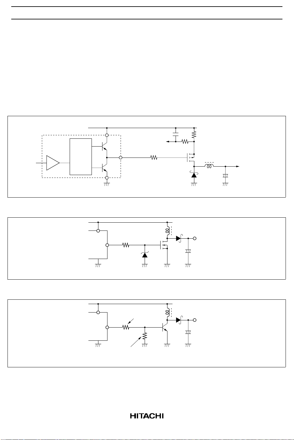
These ICs have built-in totem-pole push-pull drive circuits that can drive a power MOS FET as shown in
figure 4.1. The power MOS FET can be driven directly through a gate protection resistor.
If VIN exceeds the gate breakdown voltage of the power MOS FET additional protective measures should
be taken, e.g. by adding Zener diodes as shown in figure 4.2.
To drive a bipolar power transistor, the base should be protected by voltage and current dividing resistors
as shown in figure 4.3.
V
IN
To C
Bias
circuit
Totem-pole output circuit
P.GND
OUT
Gate protection
resistor
L
R
G
Example:
P-channel power MOSFET
V
O
Figure 4.1 Connection of Output Stage to Power MOS FET
V
IN
R
G
V
O
OUT
GND
D
Z
Example: N-channel power MOSFET
Figure 4.2 Gate Protection by Zener Diodes
V
IN
Base current
limiting resistor
V
O
OUT
GND
Base discharging resistor
Example: NPN power transistor
Figure 4.3 Driving a Bipolar Power Transistor
12
 Loading...