HIT HA16113FPJ Datasheet

HA16113FPJ
Dual Watchdog Timers
The HA16113FPJ is a multifunction device that provides microprocessor systems with the necessary
regulated power supply, monitors the supply voltage, and generates power-on reset and watchdog reset
signals. It is ideally suited for battery-operated systems such as instrumentation systems.
Functions
• Regulated power supply
• Power-on reset
• Two built-in auto-reset circuits
• Two built-in watchdog timer circuits (WDT)
• Output voltage monitoring (LVI)
Features
• Simultaneous or independent control of auto-reset outputs.
• Precisely regulated output voltage and accurate NMI trigger voltage (both ±2%).
• Low-voltage control with NMI, simultaneous RES1 and RES2, and STBY outputs.
• Independently selectable durations for power-on reset and auto-reset: power-on duration is common to
both reset outputs; auto-reset durations can be selected independently.
• Reset command input pin (CONT) for second reset output (RES2).
• WDT filter function detects minimum pulse width and maximum period of P-RUN input pulses.

HA16113FPJ
Pin Arrangement
P-RUN1
Cf1
Rf
C
R1
STBYadj
STBY
RES1
NMI
NMIadj
Re1
Re2
GND
1
2
3
4
5
6
7
8
9
10
11
12
(Top view)
24
23
22
21
20
19
18
17
16
15
14
13
P-RUN2
Cf2
R
R
C
R2
SW
CONT
RES2
C
RES
V
OUT
V
CONT
CS
V
CC
Pin Description
Pin No. Symbol Function
1 P-RUN1 Input from main CPU to watchdog timer 1 (WDT1)
2 Cf1 For connecting capacitor Cf1 to determine WDT1 filter characteristic (frequency band)
3 Rf For connecting common bias resistor Rf to determine WDT1 and WDT2 filter
4CR1For connecting capacitor CR1 to determine ton for power-on reset and t
5 STBY adj For adjusting standby trigger voltage (insert a resistor between this pin and ground)
6 STBY Standby signal output
7 RES1 Reset signal output to main CPU
8 NMI Low-voltage interrupt signal output for memory backup
2
characteristics (frequency band), power-on reset time (t
RES2), clock-off time of auto-reset circuits 1 and 2, reset high time (t
low time (t
resistor value from 100 kΩ to 500 kΩ.
RL1
and t
), and reset pulse delay at voltage drop and recovery. Use the
RL2
, common to RES1 and
on
of auto-reset circuit 1.
Recommended range: V
= 2.8 to 4.0 V
H2
RH1
off1
and t
, t
RH1
),reset
RH2
, and t
RL1

HA16113FPJ
Pin Description (cont)
Pin No. Symbol Function
9 NMI adj For fine adjustment of Vout trigger level for NMI signal (insert a resistor between this
10 Re1 For connecting resistor Re1 to determine voltage Vout for microprocessor and IC
11 Re2 For connecting resistor Re2 to determine voltage Vout for microprocessor and IC
12 GND Ground
13 V
CC
14 CS Input for detecting power supply current
15 V
C
16 Vout Regulated voltage supplied to microprocessor and IC internal circuits Connect to
17 C
RES
18 RES2 Reset signal output to sub CPU
19 CONT Input pin for resetting sub CPU on command, or when sub CPU crashes Low input at
20 SW Selects simultaneous control, in which main and sub CPUs are both reset when main
21 C
22 R
R2
R
23 Cf2 For connecting capacitor Cf2 to determine WDT2 filter characteristic (frequency band)
24 P-RUN2 Input from sub CPU to watchdog timer 2 (WDT2)
pin and Vout or ground)
Recommended range: V
= 4.4 to 5.2 V
H1
internal circuits (insert between this pin and Re2)
internal circuits (insert between this pin and ground)
Power supply input pin (operating range: 6 to 40 V)
For base control of external pnp transistor
collector of external pnp transistor
Determines reset pulse delay at voltage drop and recovery. NMI output goes low as
soon as Vout drops below NMI trigger level. If Vout remains below this level for time
t
, both reset outputs also go low. When Vout recovers above NMI trigger level, first
RES
NMI output goes high, then after time t
t
are adjusted by capacitor C
r
RES
both reset outputs also go high. Times t
r
inserted between this pin and ground.
RES
CONT causes low output at RES2
CPU crashes, or independent control, in which sub CPU is reset independently of
main CPU
Open—independent control; connected to ground—simultaneous control
For connecting capacitor CR2 to determine t
For connecting bias resistor RR to determine t
resistor value from 100 kΩ to 500 kΩ.
off2
, t
off1
RH2
, t
, and t
off2
of auto-reset circuit 2
RL2
, t
, t
, t
RH1
RH2
RL1
, and t
. Use the
RL2
and
3

HA16113FPJ
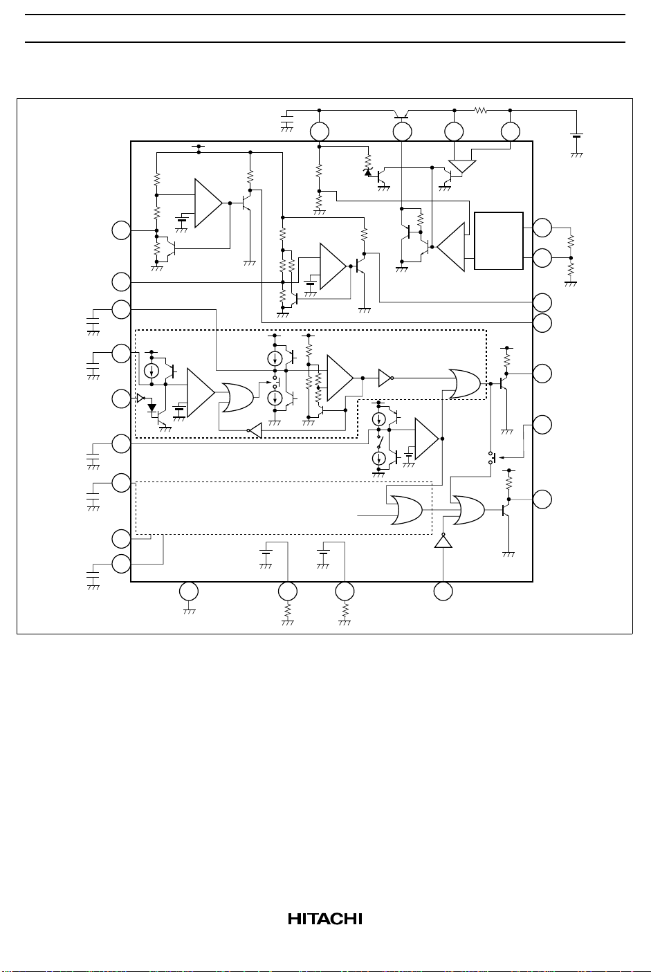
Block Diagram
STBY
adj
5
NMI
adj
9
C
R1
4
2
Cf1
1
P-RUN1
C
RES
17
C
R2
21
36.8 k
I/6
STBYdetection
block
71 k
—
31.2 k
+
19*I
—
+
16 15 14 13
3.3 k
NMI detection
block
2 k
80 k
69.7k
25 k
19 k
I
8.4 k
33 k
I*4/3
Delay circuit block
Auto-reset circuit 2
V
OUT
Over
voltage
detection
block
—
+
+
—
20 k
V
CONT
3.3 k
Regulator block
Auto-reset circuit 1
+
—
CS
Reference
—
+
Detection
block
voltage
circuit
3.3 k
3.3 k
V
CC
10
Re2
11
8
6
RES1
7
20
SW
RES2
18
Re1
NMI
STBY
P-RUN2
Cf2
24
23
I
1
RfGND
I
2
1922312
R
CONTR
4

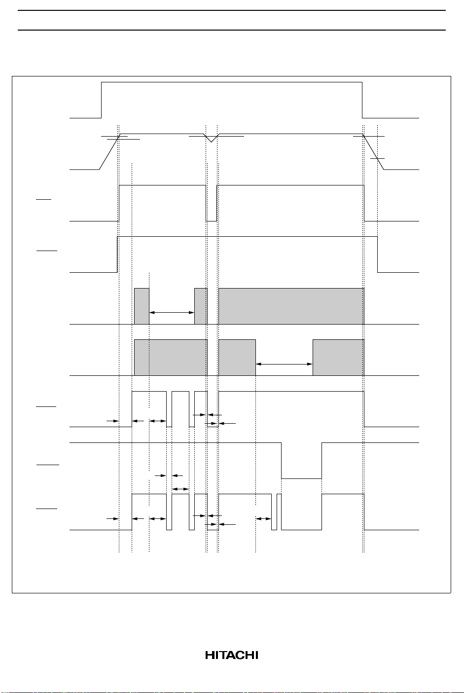
Timing Waveforms
V
BATT
HA16113FPJ
Vout
NMI
STBY
P-RUN1
P-RUN2
RES1
4.7 V
t
on
4.5 V
t
OFF1
4.6 V 4.7 V
Crash
t
RES
4.6 V (V )
NMI
3.0 V (V )
STBY
Crash
t
r
CONT
RES2
t
on
t
RL1
t
OFF1
Note: SW pin is connected to ground.
t
RH1
t
RES
t
OFF2
t
r
5

HA16113FPJ
Absolute Maximum Ratings (Ta = 25°C)
Item Symbol Value Unit
power supply voltage V
V
CC
CS voltage V
Control pin voltage V
Control pin current I
CC
CS
C
C
Vout voltage Vout 10 V
P-RUN voltage V
SW voltage V
CONT voltage V
RES current I
NMI current I
STBY current I
Power dissipation
Note
P
PRUN
SW
CONT
RES
NMI
STBY
T
Operating temperature Topr –40 to +85 °C
Storage temperature Tstg –50 to +125 °C
Note: At ambient temperatures up to Ta = 60°C. Derated by 9.8 mW/°C above this point.
40 V
40 V
40 V
20 mA
Vout V
Vout V
Vout V
5mA
5mA
5mA
600 mW
6
 Loading...