HIT HA13605A Datasheet

HA13605A
Three-Phase Brushless Motor Driver
ADE-207-201A (Z)
2nd. Edition
February, 1998
Description
The HA13605A is a three-phase brushless motor driver IC that provides digital speed control on chip. It
was developed for use as the drum motor driver in plain paper copiers and has the following functions and
features.
Functions
• Three-phase output circuit that can provide a maximum of 4.5 A at 35 V per phase
• Digital speed control
• Crystal oscillator circuit (10 MHz maximum)
• FG amplifier
• Speed monitor (lock detection output)
• Current control circuit
• Overvoltage protection circuit (OVSD)
• Thermal protection circuit (OTSD)
• Low voltage protection circuit (LVI)
• Forward/reverse switching circuit
Features
• High breakdown voltage, large currents
• Direct PWM drive outputs
• Employs DMOS
• Low on resistance: 0.7 Ω/DMOS maximum
• No lower arm flywheel diode is required

HA13605A
Pin Description
Pin No. Pin Name Function
1V
2 UOUT U phase output
3 BOOSTL Booster pin. (Low side)
4 VOUT V phase output
5 RNF Output current detection
6 WOUT W phase output
7 BOOSTH Booster pin. (High side)
8 UIN U phase input
9 VR1 Charge pump reference voltage pin.
10 VIN V phase input
11 V
12 WIN W phase input
13 C-PMP Charge pump output pin. Speed error integration and phase compensation
14 FGIN- FG Amp. (-) input pin
15 FGOUT FG Amp. output pin
16 FGIN+ FG Amp. (+) input pin
17 DIR Direction, Rotation direction set up pin
18 PWMOSC PWM oscillator input pin. Set oscillator frequency.
19 DSEL Divide select pin (L : 1/3, M : 1/12, M : 1/6)
20 OSCOUT Oscillator output
21 READY Ready pin. Speed monitor pin. (open-collector)
22 OSCIN Oscillator input
23 GND Ground
CC
X1
Power supply
Output current control voltage input pin.
of speed control.
2

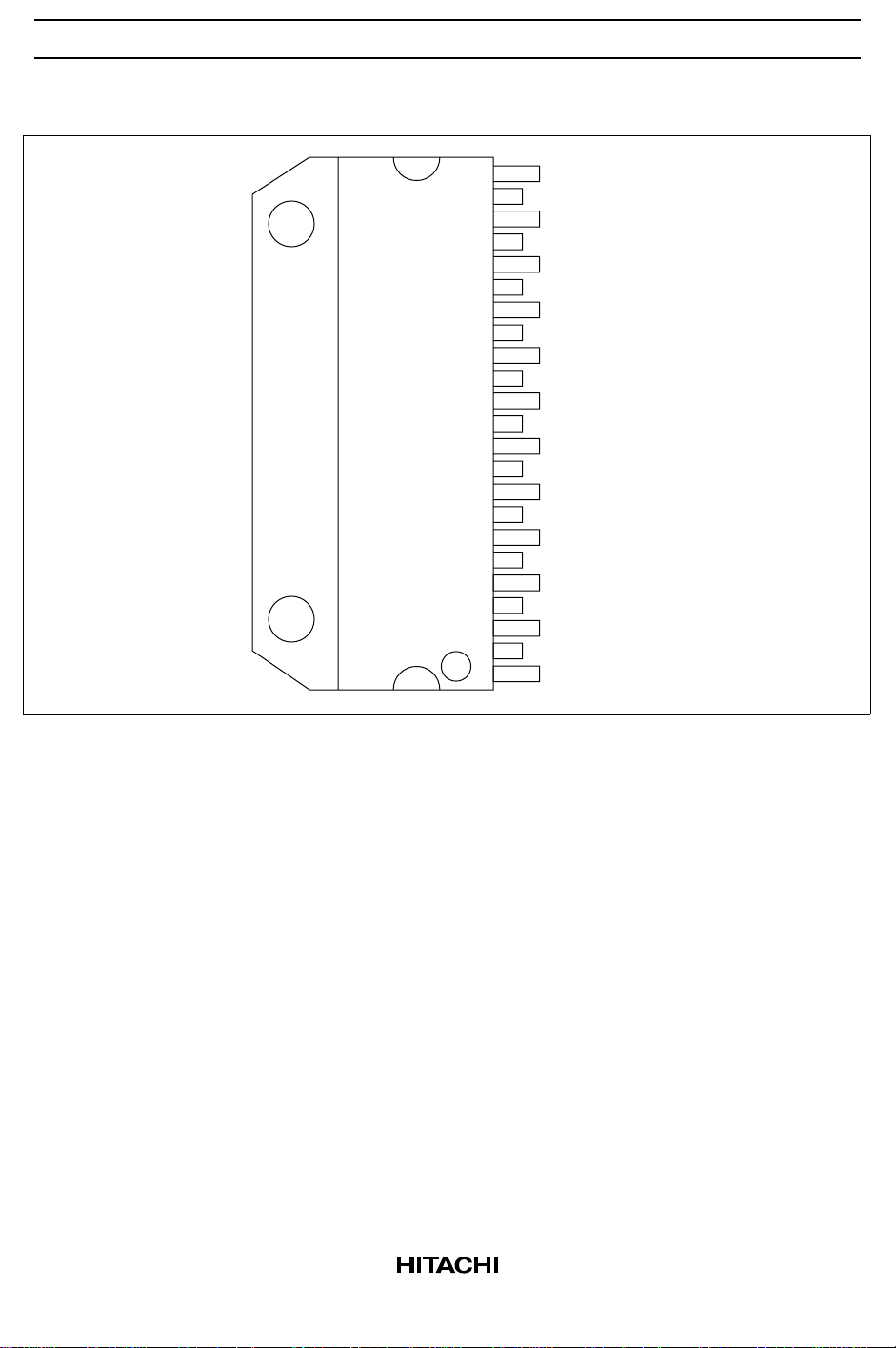
Pin Arrangement
HA13605A
23
22
21
20
19
18
17
16
15
14
13
12
11
10
GND
OSCIN
READY
OSCOUT
DSEL
PWMOSC
DIR
FGIN+
FGOUT
FGIN–
C-PMP
WIN
V
X1
VIN
9
8
7
6
5
4
3
2
1
VR1
UIN
BOOSTH
WOUT
RNF
VOUT
BOOSTL
UOUT
V
CC
3

HA13605A
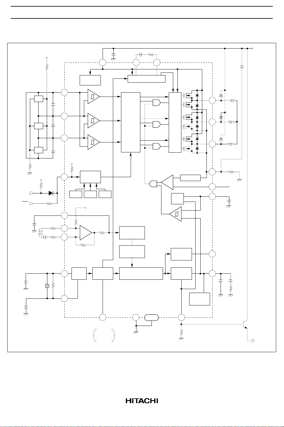
Block Diagram
5 V
R101
V
C104
1
C109
7
HL
R107
3
C110
CC
DIR
CE
C105
C107
R102
X’tal
C108
HU
HV
HW
5 V
R105
C106
D4
R106
R103
C101
C102
C103
R104
R108
8
10
12
5.6 V
17
15
16
14
22
IN
20
OUT
Reference
voltage
+
–
+
–
+
–
200 kΩ (typ.)
Control
logic
LVI
OTSD OVSD
V
23 kΩ
+
–
23 kΩ
OSC
REF
20 kΩ
1/24 fc
Divider D
19
D switching
L: 1/3
M:1/12
H: 1/6
Phase
switching
logic
FG detector
Noise
filter
Discriminator
2048
23
Booster
TAB
U
H
U
L
V
H
V
L
driver
W
H
W
L
Current
limiter
Pre-
–
+
PWM
OSC
Speed
monitor
Charge
pump
–
+
9
Filter
Clamping
R1
circuit
2
U
4
V
6
W
5
11
18
21
13
D1
D2
D3
READY
(open
collector)
C1
R
NF
V
X1
Ct
C2
R2
(≈ 5 V)
4

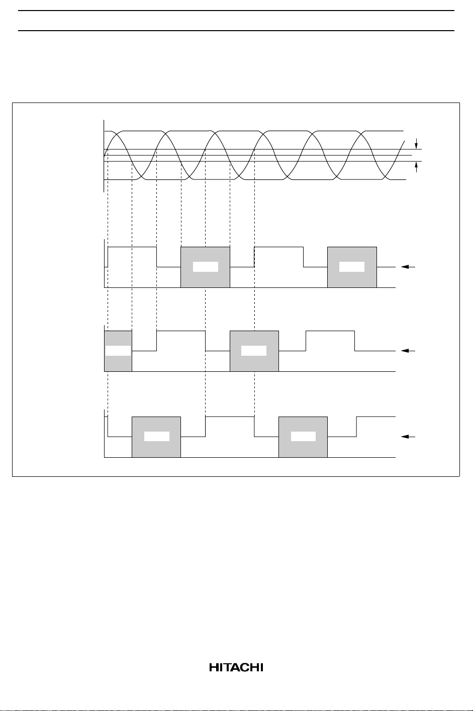
Timing Chart
FWD Mode
HA13605A
Hall amplifier
input
U output
V output
+
0
–
0
0
Hu Hv Hw
PWM
PWM PWM
PWM
Vhys
OFF
OFF
W output
PWMPWM
0
OFF
5

HA13605A
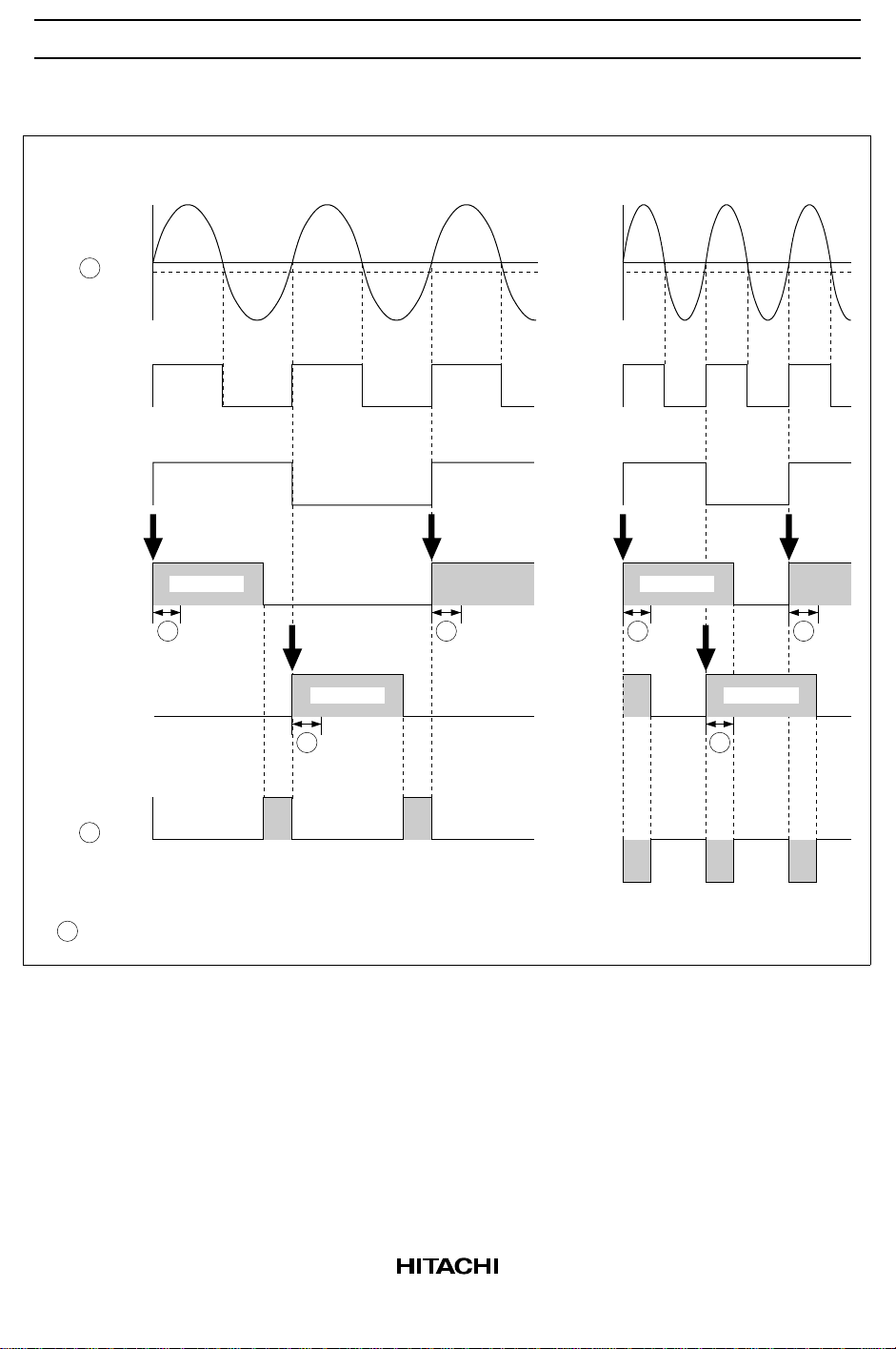
Speed control
FGout
( 15 pin)
Wave
commutation
1/2 frequency
division
(1) Slow speed (2) Fast speed
Hysterisis
1st. count
2nd. count
Charge pump
output
( 13 pin)
M : Noise cancellation (512count)
2048count
M
Acceleration pulse
2048count
M
2048count
M
M
Slowdown pulse
M
2048count
M
6
 Loading...